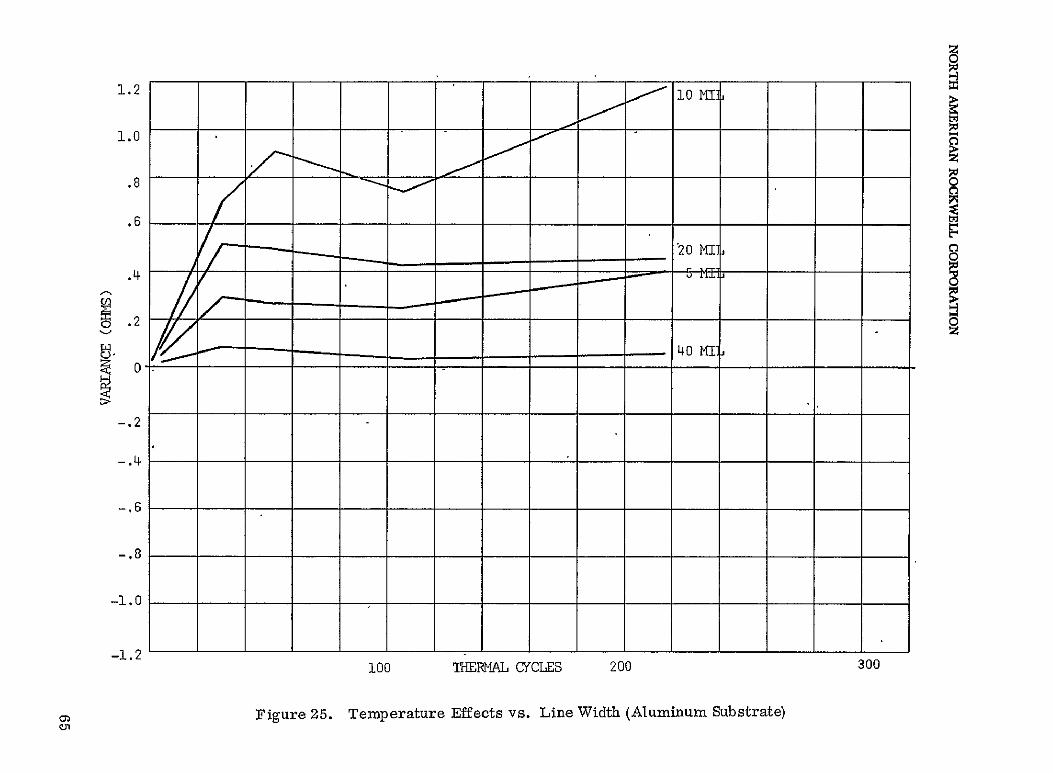
Embed Size (px)
Citation preview

ishy10
INVESTIGATION OF MULTILAYER PRINTED CIRCUIT BOARD MATERIALS
FINAL REPORT
Distribution of this report isprovided in the interest of information exchange Responsibility for the contents resides in the author or organization that 4f11t prepared it
Prepared under Contract No NAS 8-21477
by
North American Rockwell Corporation
-Reproducedby -
NATIONAL TECHNICAL INFORMATION SERVICE
Spflnsfield Va 22151
MARSHALL SPACE FLIGHT CENTER
NATIONAL AERONAUTICS AND SPACE ADMJIWRThATION
36ff~2Th- (THRU) (ACCESS1 fBER) (OE
0~
SNASACR RTMX O A 0
James F Blanche Technical Monitor
1I AS 8-21477 Marshall Space Flight Center
Huntsville Alabama
Requests for copies of this report should be referred to
NASA Scientific and Technical Information Facility P 0 Box 33 College Park Maryland 20740
INVESTIGATION OF MULTILAYER PRINTED CIRCUIT BOARD MATERIALS
FINAL REPORT
- By J E Meinhard
June 1971
Prepared under Contract No NAS 8-21477
by
North American Rockwell Corporation
3370 Miraloma Avenue Anaheim California 92803
MARSHALL SPACE FLIGHT CENTER
IATIONAL AERONAUTICS AND SPACE ADMINISTRATION
PAGE BLANK NOT FILME
CONTENTS
Page
Summary 1
Introduction 2
Artwork Used in Board Fabrication 3
Z-Direction Conductor 4
Vetal-Filled Composite 4 Organic Composite 8
Board Fabrication 14
Procedures and Sequence 14 Process Modifications and Refinements i 19 Fabrication Log 30
Board Testing 33
Preliminary Test Results 33 Environmental Testing 36 Analysis of Circuit Function in Terms of Processing 57
Conclusions and Recommendations 80
References 82
Acknowledgments 82
iii
PRECEDING PAGE BLANK NOT FILMEID
LIST OF ILLUSTRATIONS
Figure Page
1 Circuit Pattern 5 of Artwork 5 2 Via Pattern BT of Artwork 5 3 Circuit Pattern 4 of Artwork 6 4 Circuit Pattern 3 of Artwork 6 5 Circuit Pattern 2 of Artwork 7 6 Top Circuit Pattern IT1 of Artwork 7 7 Board 10 on Vespel After Step 8 17 8 Board 27 on Aluminum After Step 12 18 9 Board 23 on Aluminum After Step 16 18
10 Board 37 on Aluminum After Step 20 19 11 Board 17 on Vespel After Step 12 20 12 Modified Via Pattern B-i 25 13 Modified Via Pattern B-2 25 14 Modified Via Pattern B-3 26 15 Modified Via Pattern B-4 26 16 Top Circuit Layer (Probe Test Designations) 38 17 Distortion of Board Holder Due to Environmental Stress 55 18 Distortion of Board Holder Due to Environmental Stress 56 19 Temperature Effects vs Substrate Material 59 20 Humidity Effects vs Substrate Material 60 21 Temperature Effects vs Via Material 61 22 Humidity Effects vs Via Material 62 23 Temperature Effects vs Layer Depth (Aluminum Substrate) 63 24 Humidity Effects vs Layer Depth (Aluminum Substrate) 64 25 Temperature Effects vs Line Width (Aluminum Substrate) 65 26 Humidity Effects vs Line Width (Aluminum Substrate) 66 27 Temperature Effects vs Layer Depth (Vespel Substrate) 67 28 Humidity Effects vs Layer Depth (Vespel Substrate) 68 29 Temperature Effects vs Line Width (Vespel Substrate) 69 30 Humidity Effects vs Line Width (Vespel Substrate) 70 31 Multilayer Printed Circuit Board Failure Rates 71 32 Failure Rate vs Thermal Cycling Substrate and Via Material 72 33 Failure Rate vs Humidity Substrate and Via Material 73 34 Failure Rate vs Thermal Cycling Layer Depth 74 35 Failure Rate vs Humidity Layer Depth 75 36 Failure Rate vs Thermal Cycling Line Width 76 37 Failure Rate vs Humidity Line Width 77
V
PREQEDING PAGE BLANK NOT FILMED
LIST OF TABLES
Tables Page
I DTA Analysis of PAN Pyrolysis 9
III Possible Additives for Improving PPAN Electrical
XIV Circuit Failures Induced by Thermal Cycles at Ambient and
II PPAN Resistivity Dependence on Pyrolysis Temperature 9
Properties 10 IV Behavior of PAN in Various Solvents 11 V Catalysis of PAN Pyrolysis 13 VI Board Fabrication Log 31 VII Fabrication Process Chart 34 VIII Effect of Thermal Cycling on Circuit Resistance 35 LX Effect of Environmental Cycling on Circuit Performance 41 X Effect of Environmental Cycling on Circuit Performance 43 XI Effect of Environmental Cycling on Circuit Performance 45 X11 Effect of Environmental Cycling on Circuit Performance 47 XIII Effect of Environmental Cycling on Circuit Performance 49
at High Humidity 53
vii
INVESTIGATION OF MULTILAYER PRINTED CIRCUIT BOARD MATERIALS
By J E Meinhard
Autonetics Division of North American Rockwell Anaheim California
SUMMARY
Inherent in conventional multilayer board manufacturing methods are a number of materials factors critical to product reliability One of the more important problems relates to through-hole interconnections which in present practice involves the use of two highly mismatched materials copper and glass-epoxy laminatibns The divergence of these materials in thermal expansion properties alone particularly in the z-direction (normal to circuit planes and parallel to interconnections) constishytutes a hazard to circuit continuity in any environment where cyclic ot repetitious temperature excursions are imposed on the board Such environmental stresses canshynot be prevented without prohibitive expense and the board therefore becomes a jeopardy to the mission it is supposed to serve This risk of in-time electrical failure is augmented not only by other materials interactions but also by certain techshyniques presently required in board fabrication
The purpose of this program is to reduce the present process liabilities by developing a three-dimensional circuit technology which employs materials and techshyniques of improved compatibility
To achieve this result a multilayer board technology utilizing a polyimide plastic as the dielectric and a pyrolyzed polyacrylonitrile as a portion of the conductor network has been developed and tested The polymide in addition to providing a closer thermal expansion match even with metallic conductors proved adaptable to fabrication techshyniques and superior in stability to physical stresses of all types The pyrolyzed polyshyacrylonitizile was selected as the major component of an organic z-direction conductor after screening several classes of promising organic conductive solids Thin film metallized circuits were employed in the x y-planes
A set of internally compatible procedures and sequences was developed for the fabrication of electrically functional boards capable of reliable connection to external circuitry A total of 11 boards were completed each containing four levels of internal circuitry and one exposed top circuit Five of the boards were subjected to 427 environshymental stress cycles over the temperature range -55 to +100 deg C the final 211 cycles being conducted at 90 percent relative humidity Electrical tests before during and after the cycling disclosed that this treatment was survived by approximately 75 percent of the circuits and that it had virtually no adverse effect on dielectricshyperformance
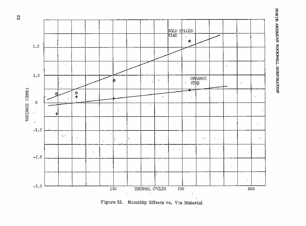
The only solder connections to the boards lost during cycling were those known to be initially defective The utilization of a thermal cycling treatment as a procedure for eliminating potential failures was suggested by the electrical data A statistical evalushyation of these data pointed to a high degree of materials compatibility with respect to thermal expansion properties but a lower degree of compatibility in regard to the combined effects of water absorption and the thermal cycling
1
INTRODUCTION
During the first year of this program it-wag shown that a process utilizing highly cured polyimide as the isolation dielectric and other organic substances for at lease a part of the conductor system was technically feasible The present report briefly reviews these results and describes subsequent effort in which substantial steps have been taken to reduce to practice the concepts previously developed
The epoxy-glass laminate system is prone to certain types of failure that can be traced to incompatibilities inherent in the materials used Outstanding among these is the highly anisotropic thermal expansion of the laminate system which ideally should accommodate simultaneously to thermally induced dimensional changes in copper conductors in the x- y- and z-directions of the board The development of a polyimide dielectric system applied layer-by-layer yet molecularly interlocked to produce the effect of an isotropic medium offered a promising route around the laminate problem In particular the large expansion mismatch in the z-direction characteristic of the laminates could be avoided
To advance even further the over-all compatibility of the materials employed replacement of metallic conductors with organic conductors (or at least partially organic conductors) also was investigated A survey of various materials to fill this role resulted in the following candidates pyrolyzed polyacrylonitrile sulfur derivatives of polynuclear aromatics (such as dibenzanthrone) and charge transfer complexes of tetracyanoquinodimethan with vinylpyridine polymers
The techniques of utilizing such materials since these required an approach entirely different from laminate technology also had to be worked out The polyimide layers for example not only had to be molecularly bonded to each other but also required a means of via etching in the z-direction (ie the direction normal to the plane of the board) in order to provide paths for conductors connecting one layer of circuitry with another or with external electrical conductors This was achieved by taking advantage of the solubility of undercured polyimide in basic solutions Etching of vias with ammonia solutions through a suitable mask was found to be feasible after which the mask could be removed and the polyimide cured to a highly insoluble condition
Except for some rudimentary experiments techniques for filling the vias with z-direction conductor were largely unexplored This was due to the fact that an application technique would be highly dependent on the organic material employed a choice that had not yet been made at the end of the first year of the program It was shown however that polyacrylonitrile applied as a thin coherent film from solution could be pyrolyzed to a black coating under the same thermal conditions as a normal polyimide cure cycle If sufficiently conductive these pyrolyzed films could become a convenient means of filling the vias
2
Various other process details had to be worked out such as the deposition and delineation of metallized circuitry on polyimide surfaces the application and removal of photopolymers and of mask materials for definition of vias as well as circuits and the special composition required by the top circuit layer to permit solder connecshytions to be made to it These objectives were achieved and at least to a limited extent the application of these process steps in sequence was shown to be feasible
It remained to prove out this apparent feasibility in terms of producing functioning boards and of demonstrating the functional survival of these boards under environmental stress which would act as an indicator of the inherent compatibility of the materials used In achieving these objectives it was proposed that a minimum of four boards be fabricated two on aluminum substrates and two on polyimide (Vespel)substrates In each pair one board was to have organic-filled z -direction conductors the other gold-filled z-direction conductors Inclusion of metal-filled conductors was proposed not only for comparative purposes but because of the incomplete stage of development of the organic conductors The boards were to have multiple circuit layers plus a top layer in which all vias terminated and to which external components could be soldered Electrical performance of the boards was to be monitored before during and after an environmental stress regime minimally including thermal cycling and exposure to humidity Following an evaluation of the test results the boards were to be delivered along with their test histories to the National Aeronautics and SpaceAdministration for further examination Achievement of these objectives is the subject of this Final Report
ARTWORK USED IN BOARD FABRICATION
In reducing to practice the multilayer board technology evolved in the preceding phase of this program it was necessary first to reach a decision on the artwork to be used in board fabrication To accomplish this it was necessary to establish certain criteria to act as a guide to selection (if possible) or design of the artwork These criteria required that the artwork be capable of demonstrating in a finished board minimally the following
1 Z-direction circuit continuity 1 to n layers
2 X Y conductivity function of line width and other dimensional and material parameters
3 X Y dielectric isolation proximity limits
4 Z-direction dielectric integrity
3
After reviewing a number of sets of artwork selection was made which provided z-direction vias in four diameters ranging from 0 040 to 0 075 inches x y line widths ranging from 0 005 to 0 040 inches xy dielectric isolation limits down to 0 005 inches and a thoroughly adequate test pattern for z-direction dielectric integrity This artwork which was designed originally for use with-conventional laminate shytechnology included a top and a bottom circuit layer and six internal circuit layers it was decided however that a five-layer board consisting of four internal layers and one top layer would serve adequately in the demonstration of program objectives The patterns utilized are reproduced (11) in Figures 1 through 6
Upon acceptance of a set of artwork the substrate dimensions were fixed (at4-34 by 5-34 in) and orders for substrate fabrication placed The requirement of substrates as a foundation for the build-up of circuit layers is one consequence of the departure from conventional laminate technology Board substrates were cut from both polished aluminum and Vespel (du Pont TM) a fully cured polyimide sheet available in the dimensions 12 x 12 x 025 in The Vespel proved to be machinable and was cut into substrates 116 to 332 in thick The surfaces were milled to reduce surface roughness
In initial experiments a first dielectric layer of polyimide was applied to several aluminum substrates using a spinning process normally employed in photoresist application To do this it was necessary to make equipment modifications to accomshymodate the larger substrate dimensions The films so formed were thermally cured up to 315 deg C Thickness was estimated to be uniform at 00002 to 00005 in with very few visible flaws
00A chrome (200 A)-gold (8000 A) layer was vacuum deposited on the dielectric layer followed by application of Riston (du Pont TM) and photoetching through mask T of the artwork (Figure 6) Visual inspection revealed no flaws in the conductor patterns- Electrical tests revealed dielectric isolation in excess of 105 ohms at the closest conductor spacings (5 mils) and a complete absence of z-direction pinholes These results were taken as a reconfirmation of the inherent adequacy of the process concept
Z-DIRECTION CONDUCTOR
Metal-Filled Composite
Gold powder of 02 micron particle size was procured for preparation of z-direction conductors The gold powder was mised with polyimide varnish (du Pont
From Engelhard Industries
4
40 rait 20 mait --n LINE WIDTHS e=====
10 rail 6 mil e------shy
jigueiF ici atenIo rwr
bull dege reg bullbullbull o o o obullbullbull oo o o4o o0 i l Obullbull VI IMTE$ bullbulloOOO5i1degO~eo~ ii i ii Oot
o S S
OO0 9 9 0 6 OO 9 -e
000 000 000 000 0
FSgSr6 2 0i tr Bo rwr
Fiur 3Cut tr-o fArwr
4 Figure 3 Circuit Pattern 4 of Artwork
6shy
$s 3
Figure 4 Circuit Pattern S of Artwor~k
6
Xx 2 Figure 5 Circuit Pattern 2 of Artwork
000 000 000 see 000
0 41 0 0 0 0 0 0
0
00
00006 00 i
0e le6 o ictPaen T fwr
PYRE ML) at a weight ratio of approximately 90 percent gold to 10 percent varnish The selection of the varnish wasa natural choice since it was the same material used for the dielectric Thus maximum compatibility of materials was assured as well as utilization of a conveniently built-in molecular interlocking process between binder and surrounding dielectric
Organic Composites
Tetracyanoquinodimethan (TCNQ) Charge Transfer Complexes - Several TCNQ complexes with polymeric materials containing electron donors had been prepared and examined during the precedingphase of this program
A reexamination of electrical resistivities of these complexes with polyshy(2-vinylpyridine) indicated that the simple salts (eg TCNQ-PVP-1 Ref 1) are stable after several weeks standing while the complex salts (eg TCNQ-PVP-3) suffer a substantial (100X)increase in resistivity in the same time period Unfortunately it was the complex salts that had the useful conductivities as experimentally confirmed preshyviously Evidently the uncharged moiety of these complexes (TCNQdeg ) was only loosely bound and readily lost to or degraded by the ambient atmosphere With it went the conductivity Some consideration was given to the possible use of the black residues obtained on pyrolysis of the TCNQ complexes in a thermal treatment equivalent to the polyimide cure cycle However widely varying weight losses (up to as high as 91 percent) had been previously observed under these conditions (Ref 1) which would have presented serious outgassing problems under repeated polyimide cure cycles and posshysibly under environmental thermal cycling It was decided that the TCNQ complexes deserved further attention only if some means could be found (or proposed) for stabilizing their compositions
Pyrolyzed Polyacrylonitrile (PPAN) - Carrying forward from earlier work (Ref 1) reinvestigation of the pyrolysis of polyacrylonitrile (PAN) was initiated using a differential thermal analysis (DTA) approach A first run revealed no significant exoshyor endothermic peaks up to a pyrolysis temperature of 400 deg C in ordinary air Although the possibility existed that any thermal excursion associated with the drastic molecular transformation might be masked by operational parameters it was not conshysidered unlikely that such an effect might be spread over a large range of temperature and therefore be difficult to detect This expectation has some precedent in the uniform distribution of pyrolyzate resistivities from 1010 to 101 ohm cm as a function of pyrolysis temperature over the range 650 to 950 deg C (Ref 2) It was considered important however to be fully aware of any existing or potential thermal anomalies before adopting (PAN)in a board fabrication process requiring multiple polyimide cure cycles at elevated temperature
After some instrumental adjustments continued investigation of the pyrolysis of polyacrylonitrile by DTA revealed a number of exotherms depending on sample preparation and container The relevant data are given in Table I
Variations in method are capable of influencing the rate of diffusion of oxygen to the polymer and the rate of heat loss from it This is reflected in the data which also indicate the pyrolysis to be a complex process The main conclusions to be drawn were that things start to happen well below the usual polyimide cure temperature of 315 to 345 deg C and were still occurring as high as 650 deg C
8
5
TABLE I DTA ANALYSIS OF PAN PYROLYSIS
Sample Exotherms PAN Inert Diluent Container (Deg C)
AS2 0 3 Powder 141-160
50 A1 2 0 3 Powder 204-229 299-320 371-382
100 None Powder 404-421 430-449 524-599 641
100 None Liquid 191-204 320-338 374-379 385-404
100 None Liquid 229-235 249-254 291-349 424-471 516-524 641-649
Temperature peaks indicating possible molecular transformations
At least two exotherms occurred below 345 deg C The question was were the molecular transformations represented thereby able to confer sufficient conductivity on the pyrolyzate A partial answer was obtained by pyrolyzing at several temperashytures and measuring the conductivities on compressed pellets The resulting data are shown in Table II
TABLE II
PPAN RESISTIVITY DEPENDENCE ON PYROLYSIS TEMPERATURE
Pyrolysis Temperature (Deg C) Resistivity (Ohm Cm)
274 (6 hours) 2 x 10¹³ 2 x 1011315
345 3 x 10
Although it is tempting to try to correlate these conductivities with DTA exotherms it is obvious that the polyimide cure temperature is inadequate for producing the desired conductivity However the specimens tested were derived from the raw powder and not from a cast film In the cast film interlocking of polymer chains might extend throughout the entire specimen body which could lead to improved intermolecular electron transport and a higher conductivity Efforts to verify this possibility in subsequent experiments (see following text) were thwarted by the fragility and loss of adhesive bonding of the pyrolyzed films
Another way to achieve lower resistivity (10 ohm cm has been reported for PPAN) was thought to be through the use of organic additives which were conductive and also oxidative An example was TCNQ others were various quinones and sulfur derivatives The main function here would be to assist in the dehydrogenation of the PAN produciig an effect analogous to a lowering of the temperature regions at which the DTA exothermal peaks occurred Three such candidates were examined and are listed in Table III along with their compressed pellet resistivity values
The last named material anthrone sulfide was prepared by a method described by Krikorian (Ref 3) This procedure consisted of refluxing the organic starting material (in this case anthrone) with sulfur in 1 2 4-trichlorobenzene at a
9
TABLE III POSSIBLE ADDITIVES FOR IMPROVING
PPAN ELECTRICAL PROPERTIES
Material Resistivity (ohm cm)
44 x 101-Dibenzanthrone 2 x 10¹⁰ (Anthrone) Sx 2 x 10⁶
Benzanthirone
temperature of about 213 deg C This process which was accompanied by an evolution of hydrogen sulfide was continued for about eight hours during which time a violet-black slightly soluble product gradually separated out The material was recovered by filtration and excess sulfur and solvent were removed by volatilization inastreamofnitrogen The material was found to be insoluble in most-solvents and essentially nonvolatile even under vacuum deposition conditions Thus it at least met the stability requirements necessary for board processing
The same process was carried out using benzanthrone and dibenzanthrone as starting materials to producethe corresponding sulfides The conversion of the benzanthrone was essentially zero that of the dibenzanthrone was practically quantitative and was conveniently monitored by the evolution of hydrogen sulfide The product was removed by filtration and purified by solvent extraction followed by vacuum sublimation to remove excess sulfur It was obtained as a deep blue-black powder having a very slight solubility in DMF (purple solution) but virtually no solubility in most other solvents Its resistivity had been reported to vary from 102 to 104 ohm em which compares favorably with the most promising TCNQ complexes previously examined without sharing their thermal instabilities
Another possible approach to the promotion of the catalytic dehydrogenation and cyclization of PAN at moderate temperature was to incorporate a catalyst of the cobalt phthalocyanine type The catalytic behavior of cobalt phthalocyanine is a matter of record (Ref 4) and probably is associated with electronic states of the cobalt atom as modified by its linkage to the nitrogen atoms of the phthalocyanine structure Samples of cobalt phthalocyanine were still available from the previous years work and no new syntheses were required
Formulations and Application Procedures - The materials investigations and syntheses of the preceding section and the formulations and application experiments described in the present section were undertaken with one main objective in view That was to utilize PAN either as its own binder or as a binder for some dispersed phase prior to pyrolysis In the latter case the dispersed solid was to serve as an organic conductor itself as a catalyst for assisting the dehydrogenation of PAN or both In every case the PAN was expected to become at least partly conductive on pyrolysis to PPAN under conditions compatible -with other steps in the board fabridashytion process It also was anticipated that these formulations would be applicable to the boards through a silk screen delineated according to Pattern B of the artwork (Figure 2)
10
The usual procedure was to disperse the PAN in a solvent to form a colloidal solution The solvent initially was dimethytformamide (DMF) which tended to produce somewhat gelatinous media (indicative of a high molecular weight polyacrylonitrile) rather than free-flowing solutions The PAN mixture then was placed in a ball mill along with the desired solid additive (eg dibenzanthrone polysulfide) and ground for several hours The milling improved fluidity to some extent but not sufficiently to make practicable its use with the silk screen (200 mesh) B pattern that had been prepared for use in via filling
This result led to efforts to improve the solvent system for PAN and to seek alternative techniques of application In the former case a number of solvent compositions were investigated and their effects on PAN are listed in Table IV The only improvement found (over plain DM3) was a mixture of DMF with dimethylsulfoxide (DMS0) The dispersion of PAN in this mixture was film-forming and easily brushable Solutions in DMF alone were more jelly-like and contractile when spread as a film Simple addition of DMF until the jelly-character disappeared resulted in a thin liquid with poor physical and spreading properties and a high conshytraction coefficient on solvent removal Introduction of DMSO permitted higher PAN concentrations which were less gelatinous and more adhesive than when DMF alone was used
TABLE IV BEHAVIOR OF PAN IN VARIOUS SOLVENTS
Solvent Effect on PAN
Acrylonitrile None visible Acetonitrile Softens slightly Dime thylformam ide (DMF) Dissolves Methyl ethyl Ketone (MEK) None Ethanol None PYRE ML Varnish None Acetic Acid (glacial) None Methylene chloride None Acetone None DM3F + acetonitrile None DMF + ML varnish None DM1 + acrylonitrile None Tetrahydrofuran (THF) None Dimethylsulfoxide (DMSO) Slightly soluble DM1F + THF Very slightly soluble DMF + DMSO Film-forming solution
An alternative to the silk screen procedure was the use of a nichrome mask in which the vias had been delineated by standard photo-etch technique A dispersion of dibenzanthrone sulfide prepared as described above in a medium of PAN and DMF alone was used in the test The thick essentially black colored liquid was applied to board Number 7 (on aluminum with three circuit layers) through the nichrome mask by a squeegee process The procedure proved mhore controllable than the
11
previous attempts with screening All through-holes so treated were completely filled and surrounding excess was easily removed after a short drying cycle The board then was heated in a normal air ambient until a temperature of 345 deg C had been reached and maintained for one hour thus pyrolyzing the PAN to an insoluble infusible and presumabl r conductive state The black deposits thus obtained appeared to be nioderatbty adherent and resistant to abrasion Electrical (probe) tests disshyclosed however that theywere extremely poor conductors and unsuitable for the intended use Concurrently it was observed that the original ball-milled dispersidn had in the course of a few days coagulated and lost its original physical properties indicating a fundamental instability of the system and a short shelf-life
The above result clearly indicated that the anticipated catalysis of PAN dehydrogenation and cyclization by the dibenzanthrone sulfide was not obtained It was evident from the literature (Ref 5) that both dehydrogenation and cyclization had to occur during high temperature pyrolysis to yield a conductive product But up to this point it had been assumed (incorrectly) that both effects would occur contiguously if not simultaneously under essentially similar pyrolysis conditions
The dehydrogenation (although not necessarily cyclization) of organic substances can be assisted by oxidants such as sulfur TCNQ etc and by catalysts such as cobalt phthalocyanine (Ref 4) Since PAN alone (and with added dibenzanthroneshysulfide) when pyrolyzed at the cure temperature of the polyimide did not yield a sufficiently conductive product it seemed reasonable to continue the search for a catalytic process that would effectively duplicate at 345 deg C results obtainable otherwise only at much higher temperatures It was known from othier sources (Ref 6) that increasing the pyrolysis temperature increased the conductivity of the PPAN The boards however were not expected to survive the temperature extremes required according to available references hence the catalytic approach
Several mixtures -were prepared as listed in Table V the intention being that the PAN in every case would act as a conductive binder after pyrolysis Each mixture was formulated- with a DMSO-DMF solvent The specimens then were painted on polished aluminum plates and allowed to dry This was followed by pyrolysis in air at 345 deg C for one hour It is clear from the results that the additives were ineffective in causing all results expected of a higher temperature treatment even though dehydrogenation might have been substantially accelerated It also would appear that the intrinsic conductive properties of the additives themselves contributed little (except in the second composition listed) to the electrical properties found
These results suggested that cyclization (aromatization) which gives rise to electron delocalization had not occurred to any great extent Therefore additional PAN samples were prepared one plain one with addedsulfur and one with added cobalt phthalocyanine and pyrolyzed in air at 830 deg C for 20 minutes
This treatment completely destroyed the first two samples and in the case of the third sample left a black residue only half the weight of the original specimen This turned out to be electrically conductive but further examination led to the conclusion that the powder was mainly cobalt oxide and contained little or no organic residue
12
TABLE V CATALYSIS OF PAN PYROLYSIS
PANAdditive Specimen Additive Ratio (ww) Resistance
Cobalt Phthalocyanine a 101 Noneonductive b
Cobalt Phthalocyanine c 110 3-x10 5 ohms
CoMn Phthalocyanine 110 Nonconductive
TCNQ-PVP-2 d 11 Nonconductive
Cobalt Phthalocyanine a 110 Nonconductive
Co Phthalocyanine a + Sulfur 110 Nonconductive
a Purified sublimate (Ref 1)
b As measured by VOM on a film approximately 0 001 in thick
after pyrolysis c Unpurified suspected of containing some cobalt oxide
d Previously prepared complex (Ref 1)
The sequence was repeated at a temperature of 660 deg C with similar results the samples lacking cobalt phythalocyanine disappearing completely It was concluded that molecular cyclization could not proceed rapidly enough to offer through laddershytype structure protection from oxidative attack This led to the further idea however that cyclization would occur independently of dehydrogenation and only at relatively high temperatures where the vibrational energy levels of the molecules would provide a high probability (and therefore rate) of ring closure Furthermore the effects of catalysts and oxidants would be negligible even though they might assist in the dehydrogenation at lower temperatures
Another set of three PAN samples was prepared and vacuum baked 30 minutes at 900 deg C and at a pressure of 50 microns During the process both sulfur and cobalt phthalocyanine were outgassed from the samples so treated Black residues were obtained in every case accompanied by substantial weight losses All were conshyductive with thin-layer resistances of two to five ohms in every case as measured with a VOM The initial presence of additives appeared to have noeffect whatever on the final electrical characteristics
The results tended to confirm the mechanism postulated above and led to the development of a standard PPAN preparation This involved heating PAN in air at 345 deg C for 1 5 hours (weight loss about 35 percent) followed by a 30 minute vacuum treatment at 900 deg C (weight loss about 75 percent total loss 83 percent) The high temperature weight loss probably resulted from the action of residual oxygen in the vacuum chamber
13
PPAN produced as above was formulated with fresh PAN (to act as binder) and solvent in a ball mill after which it was applied to existing vias in Board 9 (on aluminum with three circuit layers) which hadbeen previously delineated with a nichrome mask Curing was carried out at 345 deg C for one hour The resulting vias were found to be electrically conductive Adhesion to the gold metallization however was faulty and gave rise to mechanical flaking during electrical probing
Instead of fresh PAN polyimide varnish was used in a following experiment This was applied initially to a polished aluminum planchet and cured in the usual manner The resulting layer exhibited good electrical conductivity (with a bulk resistivity estimated at 10 ohm cm or less) and good adhesion Adhesion to gold remained to be determined but at the very least the possibility existed of establishing a strong chemical bond between the polyimide binder and the surrounding B-stage polyimide dielectric
The foregoing investigation essentially determined the z-direction organic conductor and eliminated from further consideration other conductors of organic origin previously considered It should be emphasized that the thermal treatments employed in making the PPAN did not produce graphitic material The repeating molecular unit is not the six-carbon-atom benzene ring characteristic of graphite but the heterocyclic five-carbon-atom one-nitrogen-atom pyridine nucleus (Bet 1) Furthermore the temperatures required to produce graphitic material are of the order of 2000 deg C and higher (Ref 7) which exceeds by a considerable range the temperatures employed here
The results of this investigation also tended to confirm the validity of the structural considerations adopted in an earlier phase of this program (Ref 1) and the selection at that time ofPPAN as one of the four classes of organic materials that might yield useful conductors
The polyimidePPAN organic conductor adhered well to the aluminum substrate after curing but less well to a-gold substrate on Board 10 The very large diameter vias surrounding the capacitor were particularly prone to adherence failure after cure at 345 deg C In addition film cracking apparently due to shrinkage was noted in all cases of poor adhesion The application procedure therefore was modified by removal of loose material and reapplication of fresh conductor mixture The second cure was limited to 275 deg C This dual treatment yielded intact z-direction conductors having good mechanical stability Continued attention was devoted to the organic conductor through6ut process development to ensure its compatibility with the various treatments used and to modify or improve the application technique as required
BOARD FABRICATION
Procedures and Sequence
The procedures utilized in board fabrication were developed in detail in the first period of this program (Ref 1) but only a beginning had then been made in fitting them together into a coherent process In creating a successful process it was
14
necessary from time to time to introduce remove or modify process steps Major process steps therefore will be dealt with in general terms but modifications will be described in detail The major steps are considered -below
Step 1 Polyimide Base Layer - The polymide varnish (duPont PYRE ML referred to in the following sections as ML varnish or varnish) was applied without dilution as received from the manufacturer It was stored under refrigeration (manufacturers recommendation) but was allowed to come to room temperature before application in order to avoid viscosity-dependentf variations in film thickness It has a consistency and colorsimilar to molasses The most successful technique of application was to cover the entire board with a layer of varnish then spin off the excess as normally done in photbresist applications Tools and equipment were easily cleaned with DMF Spinning speed-and-duration was adjusted according to the equipshyment used and in the direction of achieving maximum film thickness Without sacrifice of uniformity Film thicknesses so obtained were 150 to 200 microinches after cure After initial solvent evaporation at room temperature (about 30 min ) a cure to b-stage at 85 deg C (20 to 40 min)was applied At this stage the film could be masked and etched prior to final cure For the final cure temperature was advanced 2 0 to 2 5 deg per minute to a level of 315 to 345 deg C which was maintained for one hour For Step 1 no vias were required and the base layer was carried directly into final cure without isolation at the b-stage This step was applied to both Vespel and alumishynum boards Although not required for electrical isolation on the Vespel substrates it had the effect of partly smoothing out the milling marks and of providing a foundashytion layer of unvarying properties In a later modification double applications were used to increase the layer thickness (to approximately 250 microinches)
Step 2 Circuit Layer Number 5- Metallizations were vacuum deposited at 10-6 Torr from metal granules fed into a flash evaporation source For maximum adhesion a nichrome flash was first applied followed by a gold deposition in the range of 09 to 12 microns thick Riston photopolymer then was laminated to the gold surface exposed through the artwork (Number 5 Figure 1) and developed Etching of the gold layer was accomplished with iodine-potassium iodide solution (hereinafter referred to as 1K13 solution) and the nichrome with ceric sulfate solution The remaining Riston was removed with stripping solvent (methylene chloride) Visual inspection was made for delineation flaws and line continuity
Step 3 Polyimide b-stage- Immediately prior to the second varnish application the surface of the board was moistened with DMF and allowed to sodk for two to three minutes The solvent was allowed to evaporate off (or spun dry)after which the varnish was applied exactly as in Step 1 but cured only to the b-stage
Step 4 Copper Mask B-i Etch - A copper layer was vacuum deposited on the b-stage polymer and Riston photopolymer laminated to the copper surface This was followed by exposure through the via artwork (B-i) and development The copshyper layer was etched (usually with ferric chloride solution) through the Riston mask followed by careful rinsing The vias then were etched in the b-stagepolyimide layer with ammonia solution (concentrated ammonium hydroxide diluted with 20 volumes of
Formulation 225 g potassium iodide 75 g iodine and 132 g dibasic ammonium phosphate in one liter of water
Formulation 50 g ceric sulfate in one liter 10 nitric apid For masking purposes copper layers were 6000 to 8000 A thick
deionized water) without first removing the Riston mask The double mask (Riston copper) served as a valuable precautionary measure in preventing occasional diffusion of the ammonia to b-stagepolymer where it was npt desired (This was later conshyfirmed by dielectric defect density measuemnts in the large capacitor areas) Via etching usually was complete in about one minute and seldom required mechanical assistance The etched vias were permitted to bleed slightly in order to cover the exposed gold pads with an extremely thin polyimide film After drying the surface in a jet of nitrogen the Rliston mask was removed with stripping solvent The board was now ready forStep 5 If Step 5 (via filling) was to be omitted the copper mask also was stripped off andthe boardfreed of etch residues by thorough rinsing (Deionized or distilled water was specified in all solutions used) Curing then was completed at 315 to 345 deg C as specified in Step 1 and-the board was advanced to Step 6
Step 5 Fill Through-Holes - Through-holes or vias were filled individually by hand using a thin glass rod or similar instrument as an applicator This admitshytedly slow and painstaking process grew from the burrent absence -(but not technical unfeasibility) of a multiple filling process that yielded reproducible results The conductor materials applied were gold-filled 6r PPAN-filled ML yarnish as specified in the previous section Misapplied material was easily cleaned off the copper mask with the aid of DMF After filling the board was subjected to a b-stage cure cycle as specified in Step 1 The copper mask was then stripped off and the board thorshyoughly rinsed The cure cycle was completed as in Step 1 The z-direction conducshytor applications were visually examined for flaws and corrected where necessary with additional spotting of conductor mixture If this was done an additional cure cycle was applied terminating at 300 to 315 deg C
Steps 6 10 and 14 Circuit Layers - These steps were identical with Step 2 but employed artwork negatives 4 3 and 2 (Figures 3 4 and 5) respectively
Steps 7 -11 and 15 Polyimide b-Stage These steps were duplications of Step 3
Steps 8 12 and 16 Copper Masking and Etching - These steps repeated Step 4 but with artwork negatives B-2 B-3 and B-4 (See Figures 7 through 10) respectively This set of via patterns represents a modification of the original via artwork (B Figure 2) and was introduced for reasons described in the following section
Steps 9 13 and 17 Fill Through-Holes -T hese steps duplicated Step 5 but as a result of process modifications all but the final filling Step 17 were eliminated
Step 18 NichrofneCopper Deposit -A contractual requirement (Item 5 Statement of Work) called for solderability of components to the exposed top laye This step therefore was a duplication of Step 2 except that copper was substituted for gold
16
Figure 7 Board 10 Vespel After Step 8
Step 19 Tin-Plate T Pattern - Riston was laminated to the copper surface produced in Step 18 and exposed through Pattern T of the artwork The photoshy
polymer was developed to define the VT pattern in exposed copper The back and edges of the board then were masked with protection tape The board was placed in an electrolytic cell with electrical connection to the copper layer and tin-plated After rinsing the residual Biston was stripped off
Step 20 Final Etch - The T pattern delineated in tin-plate in the preceding step served as a mask for the etch removal of exposed copper and nichrome using ferric chloride and eerie sulfate solutions respectively The only material exposed to the ambient by this process was the underlying fully cured polyimide film all internal gold metallizations were completely protected The board was rinsed to remove etch residues which completed the fabrication
Figures 7 8 9 and 10 show boards at various stages of completion Figure 7 shows a board (Number 10 Vespel substrate) after Step 8 with the first two circuits Figure 8 shows a board after completion of Step 12 (Number 27 aluminum substrate) and having three circuit layers A board after Step 16 (Number 23 aluminum substrate) is shown in Figure 9 and has four circuit layers Figure 10 shows a completed board (Number 37 aluminum substrate) with five circuit layers the top layer being exposed to the environment and making electrical connection with the z-direction conductors which communicate with underlying circuit levels Two of the incomplete boards displayed certain anomalies some of which are visible and and were dropped from further processing (see following text)
17
Figure 8 Board 27 on Aluminum After Step 12
Figure 9 Board 23 on Aluminum After Step 16
18
Figure 10 Board 37 on Aluminum After Step 20
The above process step designations were utilized in abbreviated standard format throughout most of the program for periodic reporting of fabrication progress Theformat is displayed in a later section (Table VII) which summarizes this progress for
the entire period
Process Modifications and Refinements
Process modifications were made either through necessity to achieve compatishybility with other board treatments or for reasons of obvious improvement in such areas as fabrication reliability (yield) labor cost or meeting the completion schedule These modifications are considered individually below Their incorporation in the preceding processing sequence is to be assumed where not specifically designated
Blistering in Gold Metallizations - Incautious advances in cure temperatureof a polyimide layer was blamed for occasional lifting of gold metallizations mainlyin the large capacitor area A flagrant example of this effect is shown in Figure 11 (Board 17 on Vespel after Step 12) following cure of a newly etched polyimide layerA less obvious example is shown in Figure 7 also on a Vespel substrate However no significant correlation of this failure mode with substrate material could be drawn A total of seven boards were sacrificed to this cause four of them on aluminum
19
Figure 11 Board 17 on Vespel After Step 12
Although infrequent these failures were distributed throughout the manufacturing period and appeared to have no dependence on process modifications introduced in this interim
A contributing factor to the phenomenon was considered to be the chemical inertness and specular nature of the noble-metal areas which provided a poor footing for adhesive bonding to the contiguous polyimide layers A second but much more remote factor may have been ammonia penetration under the gold during the pre shyceding etching step This would have required substantial penetration of the ammonia through several layers (Ristoncopper mask green polyimide and the gold layer) during the same time (one minute) it took to etch the exposed vias The occurrence of the blistering itself tends to refute the possibility of a porosity in the metallization sufficient to admit the ammonia in the first place A more likely possibility is the action of steam generation either from water absorption over an extended period or from an incompletely cured underlying polyimide layer
The process modification in this case consisted simply of giving closer attention to cure schedules and of guarding against the omission of final cures
Adhesion of Nichrome Residues - Vacuum deposited nichrome was employed in two ways on fully cured polyimide as an anchor for a succeeding gold deposition and for a time on b-stage polyimide as a via mask The latter application gave rise to cure cycle problems which are discussed in the accompanying text In the former
20
case nichrome residues occasionally were observed to resist all attempts at etch removal These residues appeared as dark blemish areas which stained the incorposhyrated polyimide layers but probably would contribute nothing to electrical malfuncshytion
The problem was last encountered with Boards 19 20 and 21 (on aluminum) at Step 20 Etching attempts accompanied by mild mechanical abrasion caused damage to the T layer and the boards had to be recycled back to Step 18 At the same time investigation was made into probable causes of the etching failure Of prominent concern was the possible presence of passivation oxide layers on the nichrome layers that might prevent penetration and oxidation of the metal by the eerie ions Pretreatshyment of the nichrome layer by a strongly acting reducing agent therefore was investishygated This was a solution of stannous chloride (9 to 10 percent by weight) in concentrated hydrocholoric acid This treatment was found to be highly effective in assuring the complete removal of eerie sulfate in the subsequent etching step Conversely application of the eerie sulfate first tended to carry the passivation to a more refractory state and rendered the stannous chloride solution ineffectual
The process modification consisted of limiting the density of the nichrome flash and of applying a hydrochloric acid solution of stannous chloride immediately prior to eerie sulfate etching After these changes no further difficulties were encountered
Polyimide Cure Anomalous -Irreversible adhesion of nichrome residues also was observed in its use as a via mask (see foregoing discussion) on b-stage polymer A coincident observation was the excessive resistance of the b-stage polymer to via etching a problem particularly acute on Vespel boards The known poor heat transfer characteristics of the Vespel substrates (not shared by aluminum substrates) and the necessarily high thermal energy of the vaporized nickel and chromium atoms led to the hypothesis that a transient overheating had carried the polyimide cure well beyond the b-stage All visual and tactile evidence was in support of this hypothesis
Remedies were sought initially in modifications in polyinide etch compositions to include either a stronger base or a solvent additive that would increase the effecshytive basicity of the ammonia (Ammonia was preferred because of its automatic elemination by volatilization in the subsequent cure cycle) These solutions however still required the assistance of mechanical abrasion in the clearing of vias and could not be utilized in a practical fashion
Another approach deliberate under-curing of the b-stage polymer to compenshysate the expected thermal excursions likewise did not avail in solving the difficulty
A successful remedy was found only in the substitution of a lower thermal energy deposit for the nichrome in this case copper This substitution proved to have a number of advantages The copper layer resisted alkaline etches it did not anchor irreversibly to the b-stage polyimide (as had the nichrome) it was capable of sharp etch delineation it prevented irreversible bonding of the Riston to the undershylying b-stage polylanide (which was another problem with the nichrome - note following discussion) it left no visible residue on stripping from the polyimide and most important it did not result in curing the polymer beyond b-stage susceptibility to normal etching technique Vacuum deposited 6000 A 21
Over-cure effects on b-stage polyi-mide caused by nichrome deposition resulted in the loss of six boards three on aluminum and three on Vespel The three on aluminum were considered recoverable and were kept available for possible use
Over-cure by other means occurred to only one other substrate (Board 5 on aluminum) which inadvertently was exposed to an excessively high cure temperature Delamination from the substrate occurred as a result and the board was discarded
Riston Adhesion -Irreversible adhesion of Riston was encountered under three different sets of circurnstances One of these resulted in the incomplete stripping of Riston from gold metallizations after circuit delineation The final stripping was done with a methylene chloride base solvent A search for further information located a Trecommended procedure consisting of rinsing with the following sequence of solvents used stripper new stripper 10 percent methanol in trichlorethyleneisopropanol Application of this sequence in the removal of Riston from the gold metallization resulted in prompt improvement In no case was residue in visual evidence even under ordinary light microscopy Polarized light microscopy revealed occasional granules but their positive identity could not be ascertained and their cumulative effect in a completed five-layer board was expected to be inconsequential The sequence therefore was adopted for Riston stripping from circuit metallizations
At an earlier stage of process development Riston was used by itself on b-stage polyimide as a via mask Occasionally the under-cured polyimide displayed a tendency to bond irreversibly with the Riston probably during tile laminating step Some minor alterations in procedure such as reductions in time or temperature of treatshyments during and following Riston application failed to yield conclusive results Insufficient setting of the Riston resulted in insufficient adherence and loss of fine line definition Over exposure to uv irradiation due to variations in procedure also appeared to be implicated but was considered of minor consequence compared to the possible reactivity of the b-stage polyimide The problem was temporarily solved by inserting a metallization layer between the Riston and green polymer This metallization initially consisted of vacuum deposited nichrome In relatively thick layers it formed a base from which the Riston was easily stripped
The adoption of a nichrome layer however introduced other problems (as previously discussed) which led to other remedial actions including a thinning of the nichrome layer The third Riston adhesion problem was associated with the thin nichrome layers Subsequent experimental investigation showed that the nichrome was porous and could be penetrated by ammonia which produced a lifting of the nichrome film and subsequently etched away the b-stage polyimide underneath Thus if the Riston via mask was left on the nichrome film eerie sulfate was no longer required for the metal removal The observed porosity provided an explanation for the adherence of the Riston which probably was anchoring to the underlying polymer through the same pores Reduction or elimination of the porosity could be achieved with a heavier layer of nichrome but not without risk of further curing the b-stagepolymer The problem was permanently resolved by substituting copper for the nichrome as noted in the preceding section
Over-all casualties due solely to irreversible adhesion of Riston totalled only
three one of which was recycled (Board 9 on Vespel)
22
Dimensional Stability of Vespel Substrates - Vespel boards especially those of 006 inches or less in thickness occasionally displayed a tendency to warp on application and cure of the first varnish layer Application of a second varnish layer on the reverse side was ineffective or at best highly variable in reversing the distortion In a number of cases however the curvature appeared sufficiently unimportant to permit continued processing This was done since no adequate remedy or preventive measure seemed available
It was indeed found possible to apply to slightly distorted boards the various required coatings and to delineate circuit and via patterns without serious misregisshytration An unanticipated problem came to light however followinglamination of Riston to copper-coated b-stage polymer (Step 4) This took the form of localized delamination of the green polymer from the underlying layers and occurred maiily during the via etching step
The sequence of treatments leading to this deterioration suggested that the lamination step was to blame In the lamination process a warped board inevitably will be flexed due to roller pressure Since the adhesive bond of b-stage polymer to the underlying surface is immature a potential or latent delamination may ensue even though visible evidence is absent At a Later step such as etching or curing the bond weakness and deterioration suddenly become apparent This was the case with boards 12 and 13 on slightly warped Vespel substrates and also may have been the case with board 10 also slightly bowed in which some film adhesion in the capacitor area was lost Processing on these and other warped substrates was abandoned and new starts on Vespel were not continued if visible warping was introshyduced in the first application and cure of ML varnish No evidence of subsequent warping was found even in environmental stressing if the board survived the first varnish treatment Losses to this cause totalled four
Via Etching - Mask Materials The first and from a processing point of view most attractive mask material for via etching was Riston alone In its use however certain difficulties soon materialized including the irreversible adhesion of Riston to b-stage polymer as referenced above Another problem was the delicate handling required to prevent loss of fine detail particularly during inoculation with z-direction conductor This problem was aggravated by-the strong solvent action on the Riston by the DMF contained in the z-direction formulation As a result this approach had to be abandoned
In a following modification a nichrome layer was deposited on the b-stage polyimide prior to Riston lamination The via pattern was defined by the Riston mask and etched in the nichrome layer with ceric sulfate The vias then were etched in the polyimide layer followed by removal of the Riston The nichrome mask considerably facilitated the application of z-direction conductors Its use however introduced new problems To make the process work it was necessary to strike a fine balance between depositing too much nichrome which tended to bond permanently to the b-stage layer and over-cure it (see Steps 4 and 5) and too little nichrome which was porous and gave rise to irreversible Riston bonding
The third procedure which utilized copper instead of nichrome as the metallishyzation adequately resolved these problems
23
Via Etching - Metallization Protection An initially unsuspected consequence of adapting artwork from a drilled-hole type of technology to a layer-by-layer process was the lack of circuit mask protection afforded certain pre-existing vias which were not intended to make electrical contact at a given circuit level The via pattern initially used contained all the vias (Via Pattern B Figure 2) It was quickly recognizedthat a given circuit pattern would cover only the vias pertinent to that pattern while leaving the rest exposed to etchant attack during circuit delineation It was essential therefore that inoculation of z-direction conductor be made at each of Steps 5 9 and 13 (as well as 17) to prevent this attack
Although this approach was adopted it eventually proved impractical because of the temporary lack of a completely reliable squeegee process or other multiple inoculation technique An alternative procedure therefore was introduced in which via walls were permitted to bleed slightly after etching thereby extending a very thin polymer film across the gold pad The film thus formed subsequently would be fully cured and even thickened in further processing but would protect the gold from etchant penetration Prior to z-direction conductor application the protective polyimide film would be removed with the aid of alkaline reagents Concentrated aqueous ammonia appeared to be effective in this regard assisted by mechanical or air-jet action
Subsequent experience proved however that the polyimide films were extremely etch resistant Mechanical probing sometimes was successful in assisting polymer removal but occasionally resulted in damage to gold pads and shorting to the aluminum substrate A new etching procedure therefore was devised consisting of a ten-minute treatment of saturated sodium hydroxide solution at 200 deg C This was followed by a water rinse to remove the sodium salts and an acid rinse to ensure complete sodium removal The procedure could be repeated in cases where removal was initially incomplete The gold pads remained intact under these treatments by which they were readied for the final z-direction conductor application (Step 17)
Via Patterns - Two modifications in via masks were made the first and most important being the elimination of unused vias by restricting the B-patterns only to previously exposed gold pads This change was initiated not only to simplify z-direction conductor application but also to solve a more serious problem the loss of fine-line gold conductor continuity at the edges of via wells etched in the b-stage polyimide Although the discontinuities in level at these steps were only of the order of 0 002 to 0 004 in they appeared sufficient to weaken the adhesion of Riston photopolymer patterns and render them vulnerable to etch under-cut particularly in the case of fine lines
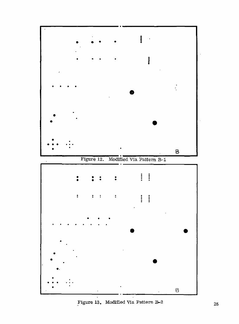
A review of previous electrical tests on partially completed boards provided some confirmation of this effect That is electrical continuity was found to be signishyficantly greater on the first circuit layer (No 5) than on succeeding layers apparently because no drops in level were involved The possibility of this problem was not considered earlier because it was initially planned to fill in alLvias with z-direction conductor after each via etch So far however this has proved impractical The new set of No B masks (designated B-i through B-4 Figures 12 13 14 and 15) solved the problem by effectively eliminating all step-downs in gold conductors
24
00
S
S - B Figure 12 Modified Via P~attern B-I
O
O
S
B
Figure 13 Modified Via Pattern 38-2 25
00
S9
S O S
deg S
090
O0
26 Figure 1 Modified Via Pattern B-S
Diameters of via patterns in the No B masks also were reduced by about 0 006 inches to improve electrical isolation between closely spaced z-direction conductors In the ammonia etching of b-stage polymer it is difficult to prevent lateral penetration Thin walls are thus rendered partly fluid and the artwork should be designed with this possibility in mind An acid stop-bath also improved process control
The discarding of step-wise applications of z-direction conductors described in the preceding section and the changes in via artwork indicated above were introduced concurrently as process modifications and assisted materially in expediting board fabrication and in improving ultimate electrical reliability
Via Etching - Reagent Quality - A somewhat elusive problem for a time was the intermittent occurrence of a tenacious etch resistance in the b-stage polyimide This problem was experienced one or more times by each of three technologists employed in the fabrication program At first the occurrence of this effect was laid to a lack of appropriate control of substrate temperature andor duration of treatment during vacuum deposition of nichrome then in use as a masking material for via etching However the sporadic occurrence of etch resistance remained essentially unchanged in frequency while the nichrome deposit was being deliberately altered in the direction of increasing thinness to eliminate polyimide over-cure Furthermore if over-cure were the cause of etch resistance a stronger base such as sodium hydroxide should have succeeded where the ammonia had failed The polymer residues in question however were found to be relatively indifferent even to sodium hydroxide
The true nature of the problem was perceived eventually to be one of ion exchange To understand it correctly it Was necessary to follow the b-stage polymer from a slightly altered point of view through the etching procedure consisting of immersing the board in an aqueous ammonia solution rinsing off with water and drying in a jet of air or nitrogen The board was then visually examined for completeshyness of removal of polymer from via wells If residues were present it was frequently found that no amount of additional ammonia treatments would avail in their removal and indeed sometimes seemed further to toughen the residues But the residues in many cases could be (and occasi6nally were) lifted out mechanically because the polymer had undergone a weakening in mechanical properties by the treatment When conditions were favorable however one or two ammonia treatments sufficed to remove all of the b-stage polymer from the vias
The b-stage polymer can be regarded as a polycarboxylic acid bound to a long organic chain that is a soap-former Addition of sodium hydroxide or any other monovalent base (e g ammonia) will convert the b-stage polymer to a soap-like product that is soluble in water But polyvalent ions convert it into an insoluble product just as ordinary soaps behave in hard water containing calcium magnesium and ferric ions Once the insoluble product is formed it strongly resists redissolashytion because the polyvalent cations hold tenaciously to the carboxyl groups B-stage polymer insolubilization by polyvalent ions proved to be the key to the problem
The corrective action taken was to ensure that accidental inoculation with polyvalent ions (e g from a contaminated water supply) was avoided in the make-up of solutions and rinsing of boards and that where such inoculation was suspected (e g from weakly acidic etch solutions) the boards were first rinsed in acid before the ammonia etch In the latter category tetravalent ceric ions used in nichrome
27
etching were considered especially harmful particularly on prolonged contact Adoption of the above measures resulted in immediate improvement and via etching became 100 percent effective
Top Conductor Layer - Composition and Procedure - The additional requireshyments of the lIT circuit layer namely that it be exposed to the ambient atmosphere and that it be capable of accepting solder connections necessitated a metal composite different from that used in the four underlying circuits These composites started with a nichromecopper deposition which was to receive a final protective metallizashytion to prevent oxidation of and facilitate soldering to the copper Process variashytions investigated included outer layer composition (tin tin-lead solder) application method (electrolytic electroless) and T circuit delineation procedure
The procedure initially involved successive vacuum depositions of nichrome and copper followed by an electrodeposition of tin-lead solder over the entire board Riston was applied and the negative T pattern exposed and developed Ferric chloride was used to remove the solder and copper layers exposed by the Riston mask The length bf time required for the etch treatment however resulted in severe undercutting and some loss of pattern resolution
In a following revision nichrome and copper again were deposited in succession This time however preparation was made to limit the tin-lead deposit only to the T circuit This required the use of a positive T pattern artwork which was used on the Riston layer applied to the copper layer Exposure and development was followed by a tin-lead electroplate after which the residual Riston was removed The tinlead plate then served as a mask for the following etches chromic acidshysulfuric acid to remove the copper and ceric sulfate to remove the nichrome The thickness of the nichrome layer however necessitated an excessively long etch treatment which again resulted in some undercutting
In another modification exactly the same procedure was followed but a thinner niehrorne deposition was specified The eerie sulfate etching again was too slow either because the metallization was still too thick or because the NiCr ratio was unfavorable Proceeding on the latter assumption (Ni-rich) an HC1 solution was substituted for the eerie sulfate with prompt results However the prolonged treatshyment again resulted in some damage including solder-plate discoloration and partial removal at isolated points Nevertheless circuit definition on the whole (5-mil lines and 5-mil spacings) appeared to be clean and exact a fact confirmed by microscopic examination
The rather granular appearance of the solder-plated surfaces led to the considshyeration of pure tin as the final layer This could be applied either by electroless or electrolytic means both of which were investigated In the electroless application the circuitry (T pattern) was masked with Riston prior to etch-removal of unwanted copper-nichrome The filled vias however were not precisely planar with the adjoining circuit layer which presented a problem of Piston adhesion at those locations This in turn introduced some vulnerability to lifting during the followshying etching step Subsequent removal of the Riston by normal solvent technique then resulted in some loss of z-direction conductor The uncertain adhesion of Riston and potential etch undercutting at via sites were sufficient basis for discarding the electroless tin method
28
In the electrolytic process Riston again was bonded to the copper-nichrome layer but in this case the T pattern was unmasked while all other areas remained protected Electrical contact then was made to the copper layer for electrodepositionof tin exactly as was done in the solder-plate process described above After T pattern deposition of the tin the Riston was stripped off and the copper-nichromelayer thus exposed etched away Undercutting still remained a problem in cases of particularly etch-resistant nichrome a problem that later was solved by a brief stannous chloride treatment (as discussed previously) prior to etching The outer tin coating thus produced was finer-grained and more uniform than the previous solder-plates and it served its intended function in protecting the copper layers
Gold-Polyimide Composite - Early electrical tests indicated a higher incidence of anomalously high circuit impedance on boards with gold-filled z-direction conducshytors than on the purely organic-filled boards This initially surprising observation was explained tentatively on the basis of the relative densities of the two fillers both of which were bonded with polyimide varnish Being 14 to 15 times as dense as the varnish medium the gold would have a tendency to settle out if the maximum packing density of the particles had not been achieved on the initial application Such settling in turn would encourage the formation of dielectric skin on top of the deposit turning the excellent insulating properties of the polyimide into a liabilityThe organic conductor even though a pyrolyzate was unlikely to have a density substantially greater than the bonding medium itself and would tend to retain its initial packing distribution
It was found possible to recover many of the high impedance sites by cautious administration of voltage pulses but such recoveries were found to be onlytemporatily effective The remedy adopted was to utilize as high a proportion of gold as possible (90 percent or better) in the z-direction conductor formulation and to abrade away excess surface films where their presence was suspected on goldshyfilled vias
Operator Dependence - Throughout the fabrication phase of this program evidence accrued suggesting an interaction between process techniques as established and the conduct of these steps by the individual operator The process consequences seemed to lie in long-term drift in control of sensitive procedures or in the sporadic appearance of recurring problems The remedies employed were to advance where possible the operators understanding of the applicable physical principles and to be watchful for signs of departure in established procedure
It will be recognized however that an operator was obliged to become master of a great variety of process techniques and to coordinate them in such a way as to minimize the time and labor required to produce each finished article Added to this was the evolving nature of the technology itself which repeatedly required the judicious application of change to process techniques In view of these considerations an operator dependence was just as much to be expected at this stage as it should be correctible at a later stage of development
29
Fine-Line Displacement - One effect that initially appeared to be operator dependent was the occasional displacement of 5-mil conductor lines which demanded extreme care in processing Although not specified as a program requirement retention of 5-mil geometry was thought to be well within the technology The particular process step investigated for a solution to the problem was the 88 deg C baking of the Riston after lamination to the metallization layer An increase in baking shy
period would-firm up the fliston and improve its mechanical strength against subsequent solvent treatments a decrease would have theopposite effect but would facilitate subsequent stripping The baking period originally 10 min was therefore increased to 18 min producing fine-line geometry considerably less vulnerable to mechanical displacement and 100 percent yield On the other hand baking of the Riston on the copper metallizations (in preparation for via etching) was reduced to five minutes or less in order to facilitate subsequent stripping This also proved successful yielding a clean delineation of vias (The hole geometry was well supported by the bulk of surrounding Piston and required only minimal cure to keep it in place the opposite situation existed in fine-line retention) The results emphasized the intershydependence of process steps and necessity for tailoring each step with full regard for the materials properties and geometries involved to achieve optimum process results
Fabrication Log
Recorded in Table VI is a summary of monthly fabrication progress Boards are identified by number in the left-hand column Start of fabrication is indicated by month at the starting position of the line following board identification Completion is indicated by a triangle Seventy-five percent of the boards on aluminum and 88 percent of those on Vespel were dropped from further processing for the reasons identified by letter symbols Many of these casualties led to improved processing techniques as discussed in the previous section Others (designated by F) suffered only minor flaws such as off-center registration edge damage (curling) minor nichrome residues etc many of which would have been recoverable by further processing Lines which terminate without a triangle or other symbol represent boards carried satisfactorily to a particular point in processing from which their continued fabrication could be resumed if later required
InTable VIE the final disposition of boards is summarized The format of this table was used in periodic reporting of progress in fabrication as defined by the major processing steps Boards 19 20 21 31 34 35 36 and 37 on aluminum and boards 11 and14 on Vespel were completed Boards 1 and 4 on aluminum also were carried to completion but with the z-direction conductor omitted because composite compositions and application methods still were under development Of the completed boards Numbers 31 35 and 36 on aluminum and 11 and 14 on Vespel were subjected to environmental stress cycling as described in the following section Not included in Table VII are boards diopped from further processing
30
TABLE VI BOARD FABRICATION LOG
Board No Mar Apr May Jun Ju1 Aug
III Sep Oct Nov Dec Jan Feb
BOARDS ON ALUMINUM
2
4
1------ ----- ------A
5
6
7-------shy8
9
10 II
---shy
--------------- ----- ---------- ---shy
12 ----- ----shy------- -shy---shy---shy
13
14
15
16
17
18
19
20
21
22
23
24
25
26
27
28
- -----
copy
-
--shy
-----(9)
-shy
-
---shy reg
----- -
-
-
Ashy
-
31
BoardNo Mar Apr
TABLE VI BOARD FABRICATION LOG (Cont)
May Jun Jul Aug Sep Oct Nov Dec Jan Feb
BOARDS QN ALUMINUM (Cont)
29 30
34
31
32
33 -
- -- -shy----shy----shy-----shy----shy-
(-shy
(-
35
36
7
-- - -- shy
------
----------------------
BOARDS oN VESPEL
A---
A
2 copy
30
4
5
6
7
8 -
- (-
-(-shy
-
10 copy
12
13
14
copy copy
A z
32
- - - - - - - - -
- - - - - - - -
TABLE VI BOARD FABRICATION LOG (Cnt)
Board
No Mar Apr May Jun Jul Aug Sep Oct Nov Dee Jan Feb
BOARDS ON VESPEL (Cent)
-15 16
17 -
Legend
A Riston Adhesion
B Over-cure
C Warping
D Diverted to Experiments
E Blistering
F Minor Defects often reparable
A Completion
R Recycled following appearance of minor imperfections
BOARD TESTING
Preliminary Test Results
In fulfilling the requirements of Item 6 of the Statement of Work which calls for exposing finished circuit boards to an environmental stress regime it was considered advisable to establish the pertinent boundary conditions well in advance of when they would be needed This action was taken on a limited scale at a time when the leading boards were only half way through processing (at Step 10) The tests were confined to three boards on aluminum (No s 15 17 and 26) each having only one buried circuit layer They were completed by inoculation with organic 3-direction conductor folshylowed by deposition and delineation of a coppertinplate T pattern (Steps 17-20) In addition to fixing exposure limits the tests could beexpected to give advance indicashytion-of any hitherto unobvious incompatibilities in materials or treatments
33
TABLE VII
FABRICATION PROGRESS CHART
Substrate Al Al Vespel
1 P61yimide base layer
2 Circuit layer No 5
3 Polyimide b-stage 3
4 Cu mask B-i etch 11 12 13
5 Fillthru-holis omit 10 omit
6 Circuit layer No 4
7 Polyimide b-stage
8 Cu mask B-2 etch
9 Fill thru-holes omit omit omit
10 Circuit layer No 3 32 33
11 Polyimide b-stage
12 Cu mask B-3 etch 17
13- Fill thru-holes omit omit omit
14 Circuit layer No 2 24 27 15 16
15 Polyimide b-stage
16 Cu mask B-4 etch 23 28
17 Fill thra-holes
18- NiCrCu Deposit
19 Tin-plate T pattern
26 Fihal 6tch -shy
Completed Numbers 19 20 21 30 31 34 35 36 and37 on Al Nuambets 11 and 14 on Vespel
Therrnally Cycled Numbers 31 35 and 36 on Al Numbers 11 and 14 on Vespel
34
After initial electrical measurements the boards were carried through eight thermal cycles from -65 to +125 deg C The single-cycle period was 267 hours The effects 6f this cycling on circuit resistance are given in Table VIII
TABLE VIII EFFECT OF THERMAL CYCLING ON CIRCUIT RESISTANCE
Resistance (Ohms) AR Line Width
Before Cycling After Cycling (Percent) (Mils)
083 082 -12 40
101 100 -10 40
204 201 -15 20
403 460 +142 10
437 456 +44 10
All circuits were of identical length with line widths as specified in the table Casual inspection of the results indicates a resistance dependence on line width placing the main component of resistance in the lines themselves Indeed a plot of reciprocal resistance against line width produces a straight line through the origin suggesting a negligible contribution from the z-direction conductors The highly favorable cross-section-to-length ratio of the vias no doubt is a contributing factor On the basis of this limited evidence however it could not be assumed that via resistance contributions would be insignificant in all cases
The effect of the thermal cycling on resistance measurements was negligible except for the two 10-m lines This suggested a possible limiting value for line width the five-mil lines in this specimen were inoperative both before and after the cycling Determining the exact cause of the resistance changes would have required a detailed failure analysis
Circuit as employed herein refers generally to a simple board element consisting of a buried conductor line including (where applicable) its z-direction conductor and T layer metallization termini It also may consist of an external resistor soldered to a pair of T layer pads and contiguous conductors or to probe sites used in testshying for dielectric current leakage
35
In a further test a two-inch length of 25-mil gold plated copper wire and an inteshygrated circuit were soldered to pads on the T circuit layer No unusual problems were encountered in the soldering process Adhesion strength of the solder bond was remarkably strong being in excess of one pound pull strength in the case of the single wire Visual examination revealed no evidence of material degradation in or near the bonding sites
Another specimen instead of receiving an electroplate of solder (Step 19) was float-soldered directly at a temperature of 257 deg C The treatment resulted in extensive parting of the circuit layers from the substrate The specimen had received no desiccation or heating to outgas moisture (which can be as high as two percent by weight of the polyimide) prior to the treatment Appropriate thermal or outgassing pretreatments should make this method a practical alternative to electroplating
In view of the preliminary results described above it was decided that the finished boards could be made to yield useful information by undergoing a prolonged series of thermal cycles both at average humidity (50 to 60 percent relative) and at high humidity (90 percent relative) but that a thermal shock treatment would have consequences drastic enough to render the boards unsuited for many subsequent tests Therefore final board testingwas confined to an analysis of the effects of thermal cycling only as described in the following section
Environmental Testing
Specimen Preparation - Environmental thermal cycling was initiated on five boards as soon as they were completed Boards 31 35 and 36 on aluminum and Boards 11 and 14 on Vespel Boards 14 31 and 36 had organic z-direction conducshytors the remainder utilized gold-filled polyimide as the z-direction conductor mateshyrial The group therefore contained all four combinations of z-direction conductor and substrate materials due for delivery under the terms (Item 3) of the contract
Electrical resistances were measured on all circuits prior to inoculation with z-direction conductor in order to ensure the detection of any significant changes introshyduced by application of these materials These data labeled IB F and A F (before filling and after filling) are conveniently combined with all subsequent resistance measurements in a single set of tables laterin this section
In continued fulfillment of the requirement to demonstrate solderability of comshyponents to the boards (Item 5) four ten-ohm resistors were soldered to each of the boards prior to cycling Some difficulty in soldering was encountered due to an
36
apparent excessive thinness of the copper layers (and probably to the presence of sufficient tin-plate) which resulted in copper depletion The problem was particularly acute where poor heat transfer conditions pirevailed ie on the Vespel boards and very short iron dwell times were required Attachment of resistors to board 14 on Vespel was only 50 percent effective (in the sense that only two of the four resistors were attached as initially planned) and further casualties were to be anticipated on prolonged thermal cycling The problem was not observed in the prior soldering experiments where only aluminum substrates were tested and the copper layer was solder-plated rather than tin-plated The observed soldering difficulty on the Vespel boards however should not be taken as an inherent flaw in the compatibility of the materials employed but as an indication that the procedures utilizing these materials require further optimization Remedial modifications such as thickening the copper deposit andor preheating the Vespel boards prior to soldering can be utilized if continued development appears justified
Test Schedule - Environmental cycling was conducted over a two-month interval toward the end of the c6ntract period The five boards identified above were exposed to 427 cycles having a three-hour periodicity and a repeating temperature excursion of -55 to +100 deg C The first 216 cycles were conducted at ambient humidity (40 to 65 percent relative) and the last 211 cycles at 90 percent RH Electrical measurements were made on the boards at 030 52 106 216 234 263 317 and 427 cycles The measurements included resistance determinations on 58 circuits per board and 17 dieshylectric leakage tests per board yielding approximately 3300 datum points that reflected the effects of the environmental cycling on electricalperformance
Selection of Test Sites - All electrical measurements are identified and coded in Figure 16 which displays the top circuit pattern in solid colors and underlying circuits as dashed lines There are four circuit levels below the T layer designated as 5 4 3 and 2 on the artwork with Layer 5 next to (but electrically isolated from) the substrate and Layer 2 next to the T layer Circuits of similar configuration are grouped toshygether under a single letter symbol Group Al to A4 for example consists of 40-mil lines with At at Layer 2 and A4 at (the bottom) Layer 5 Set B is similarly organized but consists of 20-mit lines Sets C and D have 10- and 5-mil lines respectively
Resistors R1 to R4 are soldered to the indicated pads on the T layer and lie on the board surface These pads are otherwise isolated from each other because undershylying circuits have been left out
In Sets E through L the intervening Circuits 2 3 and 4 have been deliberately omitted to preserve clarity For the same reason these circuits have been represhysented by diagonals rather than attempting to delineate their actual square Scontours (see Figure 9) which overlie each other at adjacent circuit levels Group El to E5 lies entirely at Level 5 group F1 to F5 lies at Level 4 and overlays set E Sets G and K lie at Level 3 Sets H and L at Level 2 Sets E and F consist of 10-mil lines Sets G and H 20-mil lines Sets K and L 40-mil lines
In Sets M and N probe contacts are represented by arrows situated at opposite ends of each line and designate the circuit measurement identified by the assigned
Approximately 20 000 A Rise time 90 min fall time 75 min soak time (high) 10 min soak time
(low) 5 min
37
ASC2l cRC 4D3D21D E ibKrL
000 000 so see 000 0
00 0se e s oo0 0 as geo P50i
en P7
1
O000eso bull
Legend
All underlying circuits are represented by dashed lines
All electric probe measurements are identifted by group and number and include resistances of the terminal vias where applicable
Ten ohm ( I percent) resistors R1 to R4 are soldered to the indicated surface pads whereunderlying shunt lines have been omitted
Although not explicitly represented in the diagram E2 E3 and E4 are situated sequentially between El and F6 The same applies to Groups F G H K and L Circuits in these groupsactually are square S-shaped but for further clarity are depicted as diagonals
Capacitor leakage measurements are identified by the terminals probed eg Pl-1 P22 etc Electrical leakage measurements to the substrate apply to boards on aluminum only and are identified as GR and G-p2 Consult for further details
Figure 16 Top Circuit Layer (Probe Test Designations)
38
symbol In both sets Lines 1 and 4 lie at Level 2 Lines 2 and 5 at Level 3 Lines 3 and 6 at Level 5 Lines at Level 4 are absent in both sets
Capacitor measurements are designated by P The top capacitor plate consists of two electrically isolated and independently terminated metallizations one being a central circular area with Terminus P8 the other an outer annulus with Termishynus P7 Directly beneath this pair and isolated from it by a polyimide layer lies a single circular metallization (Level 2) whose outer contour coincides with that of the top annulus P7 and which terminates at the pad identified as P5 (6 7 8) The addishytional numbers appended to this terminus serve to identify the various dielectric leakshyage measurements requiring the use of this capacitor plate Thus the designation P8-8 is the measurement between Termini P8 and P5 (6 7 8) or between the top central capacitor plate and the Layer 2 capacitor plate directly below it Similarly the designation P7-7 applies to P7 and P5 (6 7 8) or the measurement between the top annular plate and the same underlying plate
There are a total of three dual-plate combinations each consisting of a central circular plate and a coplanar annulus identified as P7 - P8 P5 3 - P4 6 and P1 GR-P2 GR They are situated respectively at Levels T 3 and 5 The intervening solid circular plates are P5 (6 7 8) at Level 2 and P1 (2 34) at Level 4 All of the plates are electrically isolated from each other and from the substrate by the thin (200 to 250 microinch) polyimide films
The dual combinations are separated by a lateral spacing of 10 mils and afford a means of testing for current leakage between adjacent conductors on the same circuit level These tests are identified in the following tables according to the dual-plate designations given above but abbreviated to (GR)P1-2 (at Level 5) P5 3 - 4 6 (at Level 3) and P7-8 (at Level I IT)
Leakage to ground pertains only to the aluminum substrates and is measured from the lowermost dual combination to the metal base The tests are identified as GR1 and GR2 in the tables
Capacitor measurements other than current leakage tests were considered but could not be scheduled in the time available
Procedure and Evaluation Criteria - Electrical tests were designed to serve three purposes to monitor fabrication techniques to demonstrate functionality of completed boards and to reveal performance trends during environmental cycling In view of the desirability of generating a statistically significant number of data and of the substantial number of test sites to be monitored therefor electrical probing by hand with a VOM was considered the only practical procedure Although some error in measurements can be anticipated as a result of small contact areas variations in conshytact pressures and occasional intervention of electrically resistive films the magnishytude of such errors was not expected to be great enough in most cases to occlude important trends in performance induced as a result of fabrication technique or thershymal cycling
Measurements were designed to determine both conductor performance and dielectric performance In both cases performance was evaluated in terms of electrishycal resistance and recorded in ohms The range of measurements was determined by
39
the instrumental capability which in this case lay from approximately 02 ohms to 5 x 10⁷ ohms This automatically established the dielectric performance criterion at 5 x 10⁷ ohms since any observable meter deflection was accepted as a failure This was known to be a somewhat generous performance limit for the polyimide because the reported volume resistivity (Ref 8 p 115) is 1017 ohm cm which in application to the present geometry yields a minimum resistance of i0-1 ohms between any two capacitor plates According to the available evidence however the detection of dielectric defects was unequivocal because their resistance values all lay below four ohms This does not remove the possibility of current leakage effects represhysented by the excluded region above 5 x i07 ohms but it does clearly identify the more serious type of defect The same standard was adopted in the detection of lateral (line spacing) current leakage between conductors and in the case of aluminum subshystrates leakage to ground
Performance criteria for conductor paths were less readily defined because of the lack of an established prior art the absence of a minimum acceptable conducshytivity based on end-use requirements and the as yet imperfectly understood effects of several of the process variables alluded to earlier in this report It was particularly difficult to decide upon qualification limits in base-line resistance values ie those values measured prior to environmental cycling Many abnormally high beginning resistance values displayed remarkable internal consistency either as a group or sequentially which bespoke an inherent stability and materials compatibility in the presence of a temporary drift in some process parameter Such data could not be arbitrarily rejected without sacrifice of numerical weight applicable to the analysis of performance trends Conseqiently all data were retained and no acceptance limits placed on base-line values
The observation of performance trends during the course of environmental cycling proved more meaningful but again necessitated the establishment of an artishyficial boundary limit upon which these trends could be judged In this case an arbishytrary selection rule would not necessarily undermine the approach to meaningful conclusions The rule adopted defined failure as an increase in observed circuit resistance to a value at least twice that of the base-line value A failure distribution based on this formula permitted tentative inferences to be drawn in the absence of a more formal and possibly less conservative definition based on actual performance rdquirements
Organization of Data - Electrical performance data before during and after environmental cycling are listed in Tables IX X XI XII and XIII The circuit board represented by each table is identified at the top by its number substrate material and z-direction conductor material The circuits measured are identified in the leftshyhand colunm according to the test site designations indicated in Figure 16 Colshyumns BF and AF list measurements made before and after filling of the vias with z-direction conductor Numerical dntries are in ohms Entries of NW stand for no detectable reading In these cases the impedance exceeds 5 x 10⁷ ohms and the circuit is presumed open Entries of Oi apply to tests of dielectric integrity and indicate no detectable current leakage or failure impedance exceeds 5 x 10 7 ohms Dashes indicate omission of measurements for any of several reasons such as total loss of a component or a section of conductor lack of meaningfulness (eg resistor sites prior to soldering leakage to ground on Vespel boards) and measurements not included in the initial test plan Other entries are self-explanatory
40
TABLE IX EFFECT OF ENVIRONMENTAL CYCLING ON CIRCUIT PERFORMANCE
Board 31 Substrate Aluminum Vias Organic
Circuit Resistance (ohns)
Cycles Comletec -55 to +100C Ditto but at 90 RH
BF AF 30 52 106 216 234 26 317- 4M
Al -- 05 0T 05 05 o6 05 o6 06 0T 2 -- 14 16 15 1 4 15 15 16 16 1T 3 -- 07 08 07 06 08 07 08 08 09 4 -- 21 14 11 11 12 12 14 13 14
B1 -- 07 09 07 07 08 09 09 09 10 2 3
---
20 09
24 11
22 10
21 09
23 10
24 12
25 11
25 12
29 13
4 -- 1sa8 18 15 18 19 19 19 21 01 10 13 14 12 12 13 13 13 13 15
2 40 14 16 15 14 16 35 43 43 45 3 14 12 15 14 15 15 25 3-3 35 43 4 24 23 26 25 25 26 27 27 2 R2
Dl 26 22 24 22 24 24 244 - 24 25 2 95 24 26 25 2T 26 27 27 28 29 3 4
7y4 50 5455
53 6I
53 -61
54 62
55 63
58 70
59 7-5
62 85
82 145
El 75 34 49 47 5470 5-9 T1 73 75 2 65 34 50 48 47 50 6o 72 75 108 3 65 67 72 T2 68 74 75 T4 74 76 4 63 63 69 68 66 T4 78 155 i6o 18o 5 F
63 36
63 36
1o6 40
107 38
107 36
12 37
25 39
1351 40
o 54
150 42
2 42 36 39 38 3T 37 39 40 54 4-3 3 36 37 39 3-9 3-7 3-7 39 40 54 43 -4 5
35 36
26 26
3-7 37
36 3-7
35 36
36 37
41 41
46 42
51 51
53 k7
G1 52 49 52 52 51 51 5 5-3 53 5-5 2 52 33 51 52 51 53 52 54 5-3 56 3 53 32 50 51 50 53 52 5-3 5-3 56 4 53 43 64 66 65 68 58 61 61 66 5 56 39 50 52 52 52 51 51 51 53
HI 20 13 14 15 15 15 16 17 ie 19 2 20 13 14 16 15 15 16 17 18 19 3 22 16 15 17 17 17 18 18 18 20 -4 19 18 19 19 1-7 18 18 20 22 24 5 21 17 19 18 18 18 19 19 19 21
K 50 26 32 31 31 33 35 35 38 2 48 25 29 28 27 28 29 32 3 - 33 3 55 43 47 47 47 48 48 49 49 51 4 5
50 53
41 41
44 44
43 42
43 L2
45 43
44 43
46 44
46 44
48shy48
41
TABLETX EFFECT OF ENVIRONMENTAL CYCLING ON CIRCUIT PERFORMANCE (Cont)
Board 31 Substrate Aluminum Vias Organic
Circuit Resistance (ohms)
Cycles Completed -55 to +106C Ditto but at 90 RH
BF AF 30 52 lu6 216 234 263- 317 427
I 18 14 16 14 14 14 14 15 15 -17shy2 20 14 l8 18 18 1- 28 20 20 23 3 17 13 -7 15 16 15 15 16 17 18 4 22 13 16 14 25 14 2-5 15 -15 17 5_ 22 14 16 15 26 15 a6 a6 15 18
T 05 09 06 07 06 06 07 07 o 2 19 1-7 19 19 19 19 19 19 20 21 3 08 20 15 15 15 15 18 19 21 24 4 06 o5 08 07 07 06 o6 07 07 08 5 _ 18 16 18 18 18 17 18 19 19 20-6 20 09 11 11 21 11 - 3 1 15 17 Ni 07 10 08 08 08 07 08 08 08 10 2 18 18 18 19 19 19 19 19 20 22 3 NR 11 12 14 14 13 19 78 7-9 84 4 07 07 07 08 08 07 07 08 08 10 5 18 22 41 4-7 46 42 48 44 4k 4k 6 12 08 08 10 10 09 13 14 5 i6
OK OK OK OK OK OK K OK PI-I OK OK
2-2 short 15 18 15 14 14 23 14 15 16 3-3 OK OK 0k OK OK OK OK OK OK OK 44 OK OK OK OK OK OK OK OK OK OK 5-5 OK OK OK OK OK OK OK OK OK OK 6-6 short 17 22 19 19 19 19 19 19 21 7-7 -- OK OK OK OK- OK OK OK OK 8-8 OK OK OK OK OK OK OK OK G -- OK OK OK OK OK OK OK OK OK 2 -- 0K OK OK OK OK OK OK OK OK
(GR)PI-2 -- OK OK OK OK OK OK OK OK- o P53-46 -- OK OK OK OK OK OK- OK OK OK P7-8 -- -- i0 o7 07 08 07 09 09 11
207 101 102 plusmn08 vO-J1 105 105 16 2 109 105 102 105 104 107 108 109 3 -- -- 199 205 101 104 103 107 108 109 4 109 lO4 101 04 103 plusmno6 io8 109
BF Before filing of vias AF After filling of vias but before conmencement of environmental cycling
f No detectable current leakage or dielectric failure
42
TABLE X EFFECT OF ENVIRONMENTAL CYCLING ON CIRCUIT PERFORMANCE
Board 36 Substrate Aluminum Vias Organic
circuit Resistance (ohms)
Cycles Completed -55 to +10C Ditto but at 90 RH
3iF AF 30 52 106 216 234 263 317 42
Al 06 06 13 08 09 08 08 07 08 09 2 10 10 16 13 13 13 12 12 13 13 3 4
1310 -25
100 09
105 12
10 11
109 12
10 13
30 21
110 26
110 33
14 42
B 08 09 13 11 12 13 12 10 11 12 2 15 45 50 48 49 52 55 90 10 150 3 4
150 07
150 10
160 16
165 15
165 15
170 18
180 39
510 18
57deg 85
63Q 47
C1 18 18 23 22 22 22 22 21 22 23 2 26 26 28 31 31 31 31 30 31 -32 3 270 250 280 28o 280 270 290 280 280 300 -4 17 18 20 22 22 22 23 21 22 31 Dl 34 35 38 42 41 41 43 41 42 44 2 60 62 66 70 68 70 72 70 70 72 3 66o 700 680 680 680 68o 710 69o 70o 7oo 4 40 55 57 58 59 65 100 220 4o i6o
28 56 51 53 53 54 92 2a0 125 150 2 28 42 43 45 45 48 110 150 190 250 3 28 50 53 50 50 52 82 98 225 140 4 3 32 39 36 36 35 38 40 42 1300 5 -- 46 52 51 52 56 95 112 130 150
F1 670 730 720 720 720 720 770 228 0 150 1620 2 660 800 800 810 810 810- 940 1090 2250 1590 3 660 700 680 690 680 680 710 690 7o0 7oO 4 5
660 660
NR 80
NR4-
NR 4
NR 770
NR 60
NR 900
NR 1000
NR NR 1090 2150
GI 40 37 46 44 43 43 44 43 44 43 2 40 38 47 45 44 44 45 44 44 44 3 40 38 46 45 45 45 45 44 45 44 4
H2
41 40 18
39 8
14
4y 45 23
45 -45 22
45 43 21
45 43 20
46 45 21
44 42 20
45 44 21
44 44 20
2 18 14 24 22 21 20 21 20 21 20 3 18 17 23 22 22 19 20 19 20 19 4 18 17 24 22 22 20 21 20 21 20
18 18 23 22 22 20 21 20 20 20 44 23 34 42 39 39 43 40 40 40
2 35 3 35 41 38 38 41 38 39 39 3 3-5 33 35 39 37 38 41 38 38 38 4 35 34 35 40 38 39 41 39 39 39 5 35 31 33 38 36 37 40 36 36 36
43
TABLE X (Cont) EFFECT OF ENVIRONMENTAL CYCLING ON CIRCUIT PERFORMANCE (Cont)
Board 36 Substrate Aluminum Vias Organic
Circuit Resistance ohms)
Cycles Comleted -55 to +1000C Ditto but at 90 RH
BF AF 0 52 do6 216 234 263 1 317 427
14 23 15 15 16 16 19 16 16 16 2 15 23 16 16 17 16 19 l6 17 lT 3 15 34 16 - 36 18 17 18 16 17 16 4 15 3-5 15 16 17 17 18 16 17 16 5 15 16 16 17 17 18 16 17 17
15 13 18 19 19 1 18 26 17 18 2 12 09 bull15 14 14 13 13 12 13 13 3 09 06 11 10 10 10 09 08 10 10 4 14 13 19 17 17 14 18 15 15 16shy
-125 10 16 13 13 11 13 12 12 12 6 10 o6 10 09 09 o8 09 0 08 08
Ni 13 -130 220 300 2T0 370 600 130 250 180 2 14 50 52 57 58 64 94 105 140 140 3 40 11 l6 15 15 14 18 55 230 40 4 13 12 13 14 14 13 20 13 14 14 5 13 12 14 15 15 14 18 14 14 15 6 NR NR NR 6400 6200 6 ko 122000 NR NR NR
PI-i OK OK OK OK OK OK OK OK OK OK 2-2 OK OK OK OK OK OK OK OK OK OK 3-3 OK OK W OK OK OK OK OK OK OK 4-4 OK OK OK OK OK OK OK OK OK -OK 5-5 OK xOK OK OK OK K OK OK OK 6-6 oK OK OK OK OK OK OK OK OK OK 7-7 -- K K OK OK OK OK OK OK OK 8-8 -- 03 09 o6 06 08 08 06 o6 06
GB) OK OK OK OK OK OK OK OK OK OK 2 o OK OK OK OK oK OK OK OK OK
(G)Pa-2 QX OK OK LOK OK OK OK OK OK OK P5-346 OK OK OK OK OK OK OK OK OK OK P7-8 -- OK OK OK OK OK OK 0K OK OK
100 102 102 101 04 102 102 102 2 100 -12 103 101 104 102 104 102 3 100 102 102 102 104 102 103 102 4 100 102 102 102 lo4 102 104 102
BF Before filling of vias AF After filling of vias but before commencement of environmental cycling
No detectable reading Impedance exceeds 5 x 10⁷ ohms and circuit
is presumed open
No detectable current leakage or dielectric failure
44
TABLE XI EFFECT OF ENVIRONMENTAL CYCLING ON CIRCUIT PERFORMANCE
Board 85 Substrate Aluminum Vias Gold Filled
Circuit Resistance (ohms)
Cycles Comleted -55 to +1000C Ditt6 but at 90RH
BF AF 30 52 106 216 234 263 317 427
Al 05 -20 10 09 09 07 07 68 08 09 2 10 24 14 15 15 12 13 13 13 14 3 85 100 95 93 96 96 100 102 102 102 4 o6 16 10 15 10 09 09 09 09 10
Bi 08 18 11 09 08 10 10 10 10 -1 2 16 26 20 20 19 20 20 21- 21 21 3 125 250 230 240 240 250 250 230 280 190 4 10 12 -13 12 11 12 13 13 13 14 c 17 20 21 19 19 20 20 20 20 21
2 30 80 72 68 77 190 75 63 65 2P00 3 Z10 3000 1500 1750 1850 2100 1600 2100 4400 4500 4 20 24 26 24 23 23 24 25 25 26
D1 34 42 43 43 41 43 46 46 46 47 2 60 150 160 60o 180 220 150 150 3300 14O 3 510 650 660 i25o 62o 65o 670 670 690 72o 4
El 55 35
72 40
75 -40
68 39
63 39
66 40
68 41
70 41
20 42
8 43
2 34 40 4o 39 38 41 41- -4 41 43 3 34 40 40 39 38 40 41 40 41 42 4 34 40 39 39 38 40 40 40 41 42 5 35 41 40 41 40 43 43 4 -6246
F1 50-5 800 720 720 540 560 580 580 580 600 2 505 600 680 660 66o 670 690 690 700 800 3 805 680 840 880 900 830 670 670 760 7 -4 505 580 570 570 560 57 59Q 590 620 70 5 505 550 560
01 36 40 40 - 520 50 5 41 -042 4-3 2 35 44 43 43 43- 45 46 44 45 46 3 36 46 46 46 46 48 48 4S 49 50 4 36 28 42 42 41 L3 44 42 44 44 5 36 30 48 77 72 64 63 62 63 10o 2 16 20 19 19 18 19 20 19 20 21 2 16 20 20 19 18 20 21 20 20 21 3 17 20 20 20 19 20 21 20 21 21 4 17 20 20 21 19 20 21 20 21 21 5 17 22 20 20 19- 20 21 20 21 21
K0 29 25 1000 1250 1950 -- 11000 5600 i000 2000 2 29 3-7 37 35 34 36 37 36 37 38 3 29 38 38 37 35 37 38 38 39 39shy4 29 42 45 45 47 47 52 52 53 45 5 30 26 58 56 53 57 54 53 43 flo
45
TABLE XI (Cont) EFFECT ON ENVIRONMENTAL CYCLING ON CIRCUIT PERFORMANCE (Cont)
Board 35 Substrate Aluminum Vias Gold Filled
Resistance (obms)Circuit
Cycles Completed -55 to +oOC Ditto but at 90 RH
BF AF 30 52 106 216 234 263 317 427
L 12 17 17 16 14 15 16 17 16 1T 2 12 17 17 16 17 16 17 16 17 1T 3 13 17 17 16 15 16 17 17 17 18
16 16 16 184 13 15 17 1-5 i6 - 5 13 15 17 16 16 16 17 17 17 17
ba 08 12 14 11 10 10 11 1 11IT 2 10 36 N1t 2250 1850 1500 2500 34 36 3-4 3 o4 08 10 o7 06 07 08 07 08 08 4 09 14 14 12 11 12 1-3 13 13 13 5 10 29 35 34 32 37 40 35 37 27 6 o4 11 10 08 07 07 09 08 08 09
Ni 10 15 18 17 14 1-5 16 16 17 - 2 14 70 70- 7600 4 800 7500 870 9500 10000 1000 3 05 29 760 38 670 1300 55 31 39 39 4 10 15 17 15 13 13 15 14 14 16
5 12 200 620 350 115 4500 3000 90 92 78 6 05 1100 22000 67000 60000 40O00 6000 1100 1000 2000 P1-IO 0K OK OK OK OK OK (A 2-2 OK OK OK OK OK OK OK OK OK OK
OK OK3-3 OK OK OK OK OK OK OK OK 4-4 OK OK OK OK Ox OK OK OK OK OK
5-5 OK OK OK OK OK OK OK OKOK OK
6-6 OK OK OK OK 17 16 15 17 17 18 7-7 - OK OK OK 01 OK OK OK OK OK 8-8 -- OK OK OK Ox -OGK 01 OK OK OK
GRJ OK OK OK 0x OK OK OK OK OK OK 2 OK OK OK OK OK OK OK OK OK OK
(GR)Pa-2 OK OK OK OK OK OK OK OK OK OK P53-46 OK OK OK OK OK OK OK OK O OK P7-8 -- 08 11 08 05 06 09 OK OK OK R -- 100 101 100 100 104 103 106 109 2 100 101 100 - 100 104 103 106 116 3 100 100 100 100 102 103 106 109 4 100 101 100 101 105 106 106 i0
BF Before filling of vies AF After filling of vias but before commencement of environmental cycling
NNo detectable reading Impedance exceeds 5 x 10⁷ ohms and circuit is presumed open
-No detectable current leakage or dielectric failure
46
TABLE XII EFFECT OF ENVIRONMENTAL CYCLING ON CIRCUIT PERFORMANCE
Board 14 Substrate Vespel Vias Organic
Circuit Resistance (ohms)
Cycles Completed -55 to +1000C fitto but at 90 RH
BF AF 30 52 106 216 234 263 317 427
Al 09 250 820 1600 2500 1200 2000 Damaged -- -shy2 3
12 12
10 10
13 12
12 12
12 11
13 12
15 5xZ10 5
16 16 21 19xl0515xl05 1lxl05
4 20 20 22 22 21 23 550 660 640 38o B1 12 13 14 13 12 13 13 13 1i 16 2 12 56 68 67 67 68 90 96 91 lO1 3 4
02C
15 35 17
12 40 16
17 52 19
15 370 18
14 420 18
16 520 19
17 6500
20
NR 8000
18
NR HR 1i04 N
16 22 2 23 25 25 25 24 25 26 24 22 27 3 27 25 28 28 26 28 29 29 27 34 4 50 48 53 5-3 53 5-3 250 230 260 20
D1 35 3-3 36 36 3-5 36 40 380 450 420 2 42 180 380 490 620 270 80o0 9000 1000 1002 3 65 65 72 72 7-3 125 80 90 2x0 4 5xlO 4 130 320 195 146 135 180 NE l2l5 NE LX
El 120 120 127 126 5 16 120 120 130 140 2 20 120 111 121 117 13 210 118 2xlO5 NR 3 4
120 NR
100 100
340 122
370--12
360 111
400 115
680 130
670 160
680 2x10⁴
N 2x0 4
5 14o -20 325 12 222-i o 16o ooo 0L0 4oo Fl 48 4 4 50 49 47 - 48 48 49 49 70 2 48 46 49 48 47 48 47 48 52- 75 3 65 44 49 47 46 47 48 50 52 NR 4 5
70 55
300 44
2200 70
2200 150
2600 300
3000 90
1300 NE
1500 NR
3x10⁵
NE NR NE
G 25 24 29 28 27 27 27 27 26 3-2 2 25 23 29 27 26 27 NR NR NR 5x1O 3 24 25 30 29 27 29 6XU04 NR 4xlO5 N 4 30 24 29 29 26 27 70 66 59 NR
24 24 3 31 28 30 30 30 28 52 HI 23 60 72 68 6 8 0 75 11O0 1600 2500 2 23 21 30 26 26 26 25 25 21 26 3 23 NR NR NR NR NR NR NR NR NRshy4 22 25 41 88 110 33 830 9004 730 50 4 5 3 25 47 43 43 45 o0 8x0 I5x105xx10
K) 24 25 22 24 2 22 23 23 22 28 2 22 23 23 23 22 22 21 22 19 22 3 21 19 23 23 22 21 22 22 19 22
-4 20 18 23 23 22 22 22 24 25 31 5 20 19 22 23 22 22 22 22 20 25
47
-- -- -- --
TABLE XII EFFECT OF ENVIRONMENTAL CYCLING ON-CIRCUIT PERFORMANCE (Cont)
Board 14 Substrate Vespel - Vias Organic
Circuit Resistance (ohms)
Cycles Conmieted -55_to +100degC Ditto but 90 RH
BF AF 30 52 ao6 216 234 263 - 317 427 4
Li 19 90 820 940 670 1000 2000 2lx104 4x104 Tx0
2 19 17 23 22 22 21 25 27 25 31 3 19 17 24 21 21 21 22 140 3500 3900 4 19 200 1200 3700 3709 1 5x10⁵ NR NR NR NH 5 19 140 550 520 580 6r0 1200 2300 2000 2400
Pa 11 20 23 23 26 25 22 20 18 22 2 35 500 1200 1350 1600 1650 8000 7500 8000 t000 3 18 19 19 19 2-3 - 34 750 1000 1090 2200 4 11 25 28 29 26 28 30 2 25 2-7 5 11 27 28 35 3-3 35 23 24 22 26 6 17 16 14 - 4 13 i4 14 14 14 950
N1 10 28- 41 43 43 46 46 42 38 44
2 13 300 62o 66o 670 780 680 650 570 1100 3 32 -850 3600 42oo 48o0 5000 5000 5500 7500 1000 4 09 70 132 145 165 230 370 280 240 380 5 15 140 175 190 17-5 175 190 170 150 160 6 23 35 21 22 21 22 24 26 600 3500 PO- OK OK 0K or oK OK OK OK OK OK 2-2 OK OK OK OK OK OK OK OK OK 0K 3-3 25 35 21 - 17 17 18 8 18 18 25 4-4 19 20 09 09 09 10 10 11 10 17 5-5 OK OK OK OK OK OK OK OK OK OK 6-6 OK OK O OK OK OK OK OK OK OK 7-7 -- OK OK OK OK OK OK OK OK OK 8-8 -- OK OK OK OK OK OK OK OK OK
-GK1 - -- -- -- shy
2 - -- shy
(GR)PI-2 OK OK OK OR OK OK OX OK OK OK P53-46 23 30 -23 22 20 20 20 20 18 21 P7-8 -- OK OR OK OK OK OK OK OK OK
105 103 102 102 115 160 NR- RPa 2 -= Lost -- -- -- --
3 105 103 102 lo4 103 103 101 105 4 - NR NR N NR NR NR NR NR
BF Before filling-of vias A-F After filling of vias but before commencement of environmental cycling
No detectable readings Impedance exceeds 5 x 10 ohms and circuit is presumed open
M-Nodetectable current leakage or dielectric failure
48
TABLE XIII EFFECT OF ENVRIONMENTAL CYCLING ON CIRCUIT PERFORMANCE
Board 11 Substrate Vespel Vias Gold Filled
Circuit Resistance (otms)
Cycles Completed -55 to +000C Ditto but at 90 RH
BF AF 30 52 106 216 234 263 317 427
Al 23 35 30 24 23 26 27 28 29 48 2 28 25 23 16 15 17 19 19 22 27 3 09 14- 11 07 07 07 08 08 08 1l 4 08 19 14 11 11 13 12 14 15 19 B 36 44 3-7 36 36 36 37 36 38 40 -2 30 30 25 24 24 24 25 25 25 27
3 09 12 25 3700 300 2200 1160 18 30 4 13 5 1 1 1 15 17 17 18 21 c 60 70 65 63 62 62 65 63 63 65 2 75 50 46 42 41 41 45 44 44 46 3 17 23 21 17 16 17 18 18 21 23 4 24 31 29 26 25 26 28 29 33 46
D1 110 120 118 118 115 115 110 20 20 125 2 80 85 84- 82 82 81 86 85 90 170 3 30 4o 33 30 30 30 36 46 850 120 4 70 80 77 76 75 75 80 80 84 96
El 60 75 64 61 61 62 70 69 69 86 2 150 75 63 59 59 60 67 69 71 78 bull3 55 75 62 59 58 60 67 69 8o NR
4 55 60 63 62 62 62 67 71 90 220 5 5-5 70 87 780 1150 36 2500 1000 2800 NE
Fl 22 26 28 25 23 24 27 25 26 N 2 22 25 28 24 23 23 27 25 29 32 4 3 29 3-7 NR 2000 8500 2500 4x10 5000 NR 3x10 4 5
NR 36
72 3-7
2300 39
1450 37
1350 36
200T 36
7000 40
1800 44
2700 80
3100 NR
G1 50 52 5-5 53 53 53 57 55 -66 55 2 60 53 53 52 52 51 55 53 53 55 3 iOO 54 56 54 54 54 60 60 60 62 4 100 45 48 47 57 58 4200 5500 70 80 5 6s 45 47 46 55 56 59 58 59 60
80 60 58 57 57 57 60 56 84 84 2 80 60 61 58 58 58 63 58 88 9-o 3 75 85 83 84 83 82 87 80 74 85 4 75 80 78 79 77 77 82 75 79 82 5 S
75 42
8075
774
7739
7638
8038
79 43
75 40
77 53
78 53
2 46 48 45 45 43 42 47 44 59 64 3 44 45 48 46 45 44 49 47 50 56 4 220 45 51 49 49 49 80 80 83 85 5 50 5h 60 57 55 55 62 60 64 66
49
TABLE XIII EFFECT OF ENVIRONMENTAL CYCLING ON CIRCUIT PERFOBIMANCE (Cont)
Board 11 Substrate Vespel Vias Gold Filled
Circuit Resistance (ohms)
Cycles Comleted -55 to +100C Ditto but at 90 RH
BF AF 30 52 106 216 234 263 317 427
77 T4 7-3 73 83 80 90 9x10⁴ Li 80 8-5 2 75 85 74 68 68 68 84 11o 120 250 3 65 80 75 71 69 7o 79 95 102 100 4 11o 8o 73 68 102 102 a20 fl5 143 6500 5 60 7-2 66 220 - 220 220 -4200 5500 270 6500
Ml 3-5 44 340 1500 5-3 1800 850 115 1350 700o 2 15 2000 45x10 4 35104 43x104 2000 2500 4x10 5xo 100
-3 08 350 22 18 18 16 18 8 25 250 4 36 34 39 36 36 36 46 55 65 1450 5 15 -1000 _940 620 580 19 21 50 36 60 6 08 12 16 11 11 11 20 24 30 350
NI 40 46 4-5 42 42 42 44 42 43 4V 2 22 28 28 23 23 23 24 2-3 24 26
3 11 28 34 35 26 26 38 23 34 40 4 34 46 3-9 36 35 3-5 37 35 37 39 5 28 28 23 19 19 19 21 24 29 35 6 11 25 19 13 14 13 15 17 1 19
PI-I OK OK OK OK OK OK OK OK Ot OK
2-2 OK OK OK OK OK OK OK OK OK OK 3-3 OK OK OK OK OK OKc OK OK OK OK 4-4 Ot OK OK Ox 0K OK OK OK OK OK 5-5 OK OK OK OK OK OK OK OK oC OK
6-6 OK OK OK OK OK OK OK OK OK OK
T-T -- OK OK OK OK OK OK OK OK OK
8-8 -- OK OK OK OK OK OK OK OK OK 0B1 --- --
(GR)P1-2 OK OK OK OK OK OK OK OK OK OK P53-46 OK OK OK OK OK OK OK OK OK OK P7-8 -- OK OK OK OK OK OK OK OK OK R1 107 109 102 105 NRw NR NR NR
2 -- -- NR NR NR NR NR NR NR NR 3 N NE NE NE N NE NE NR 4 105 10k 102 101 Lst -shy
BF Before filling of vies AF After filling of vias but before
commencement of environmental cycling
No detectable readings Impedance exceeds 5 x io7 ohms and circuit is presumed open 4No detectable current leakage or dielectric failure
50
The base-line values are listed in the column headed AF 1 and serve as 0-cycle readings for the environmental stress data following The column headed 112l 6 1 also is equivalent to the 0-cycle starting point for the high humidity test results listed to the right However in the high humidity series as in the normal humidity series failure is defined only on the base-line values in column AP
Initial Summary of Results - A superficial examination of the data listed in these tables suggests that stable circuit performance is well within the bounds of the technology under development but that much yet needs to be done in optimizing process techniques to achieve a favorable yield factor Although not directly measured the compatibility of the materials used in this process appears to be borne out by the results
A comparison of BF and AF 1 entries indicates that inoculation with z-direction conductor may produce either an increase or a decrease in resistance On a single board this may equal or exceed 25 percent of the average BPIvalue An increase in resistance normally would be expected since the conductor applications (including the T layer metallization) add further elements to the original conductive path A persistent decrease particularly of the size exhibited by Board 31 (Table IX) therefore requires some interpretation It is possible that probe conshytacts to the gold metallizations in the BFseries of measurements on this board were generally faulty due to possible etching damage to the gold Filling with z-direction conductor could be assumed to establish more intimate and larger area contact with these metallizations than was achieved in probing Another possibility is that the metallizations in Board 31 were consistently thinner than in most of the other boards again leading to reduced electrical contact on BF I probing This seems unlikely however because each metallization is independently deposited which would lead to a dependence of resistance change on circuit level Such a dependence does not appear to be supported by the data A third possibility is the presence of a systematic opershyator error which was reduced or eliminated in subsequent sets of measurements The first set of measurements taken was the ITBF series on Board 31 services of the same operator were employed on all succeeding measurements A more detailed analysis of the data may yield further insight into the origin of this reduction of elecshytrical resistance following completion of the last four fabrication steps
Board 11 on Vespel also showed a slight tendency toward a negative resistance increment between ti BF and AF readings The trend is somewhat obscured by a few anomalously high readings and is considerably less general than that in Board 31 The degree of significance here will depend on further analysis If the effect actually is significant on Board 11 a correlation either with substrate material or with z-direction conductor material would appear to be ruled out
Also of process interest are the absolute values of the resistance increments Examination of the data from the remaining three boards (No s 36 36 and 14 Tables X XI and XII) reveals a positive increment of the order of 16 ohms or 08 ohms per via if the data from highly failure-prone circuits (i e circuits that failed after the first 30 thermal cycles) are excluded This would appear to be a tolerable via resistance for a great majority of multilayer board applications Of second order importance are the correlations of via resistance with cross-section depth and z-direction conductor material It will be recalled that gold-filled conductor
51
materials have tended to exhibit resistances higher than the organic-filled materials possibly because of skin effects This trend is perpetuated in the three boards under consideration the average resistance increment being distinctly higher in Board 35 (TableXI) than in the other two boards
In the succeeding exposure of the boards to 427 environmental stress cycles another distinct grouping of data emerged This was the set of current leakage tests across dielectric regions including capacitor dielectrics line-spacings and leakageshyto-ground In marked contrast to the conductive paths the dielectric displayed a remarkable immunity to the cycling in all categories In a total of 61 test sites olily one new failure appeared and another recovered both on Board 35 (TableXl) for a net change of zero defects in an original total of eight Of probable significance fs the fact that the single recovery occurred to a line-spacing defect situated in the T layer where environmental stresses could exert a prominent effect on surface contaminashytion or foreign bodies The recovery was observed after the first 18 cycles at 90 pershycent relative humidity and appeared to be permanent
At the termination of environmental stress exposure six of the defects were found 5 be associated with capacitor dielectrics involving a total plate area of 225 cm 2 Assuming each defect to be due to only onebreach in the dielectric the resulting
-2defect density in the total dapacitor area was 0 024 cm
The terminal line-spacing defect count (10 mil conductor separation) was two in a total spacing length of 137 em Assuming again that each defect was due to a single discontinuity the defect frequency was 0 015 cm-1
Another distinct group of data pertains to the resistors soldered to the boards prior to thermal cycling As previously indicated difficulty in soldering the resistors to Vespel boards led to the expectation of a high mortality rate during environmental stressing This proved to be true Of eight resistor sites on the two Vespel boards four were functional at the beginning of stress exposure and only one at the end On the three aluminum boards however all twelve resistors were functional both initially and after the exposure The resistance measurements invariably confirmed on all boards the nominal 10-ohmn values except immediately prior to functional or physical loss Probe contact in these measurements was made on contiguous conductor lines in order to include the solder connection entirely Minor modifications in processing and soldering technique as suggested earlier should be capable of resolving the probshylem of component soldering to Vespel boards -
The remaining bloc of data pertains to the resistance of conductive paths Applying the definition of failure given above (see page 39) it is immediately evident that degradation of electrical function occurs in a significant number of circuits as a result of thermal cycling particularly at high humidity In fact the incidence of failures is almost five times as great at 90 percent than at 50 to 65 percent relative humidity The data are summarized in Table XIV
52shy
TABLE XEV CIRCUIT FAILURES INDUCED BY THERMAL CYCLES AT AMBIENT AND AT HIGH HUMIDITY
Failures Failures Added
Circuits After at Board Z-direction Initially 216 90 R H Total
Substrate Number Conductor Functional Cycles (211 cycles) Failures
Aluminum 31 Organic 58 0 11 11
Aluminum 36 Organic 56 1 12 13
Aluminum 35 Gold 56 7 -2 5
Vespel 14 Organic 50 5 24 29
Vespel 11 Gold 55 2 11 13
Totals 275 15 56 71
The results show that the toll is about five percent of the initially functional circuits at the more moderate humidity condition and about 20 percent at high humidity Since the effects should be additive exposure of the initial boards to high humidity alone would have caused 26 percent of the initially functional circuits to fail
On the aluminum boards a total of 17 percent of the 170 originally functional circuits failed On Vespel the total was 40 percent of an original 105 circuits Omitshyting the terminal high humidity exposure however the corresponding proportions are 4 7 percent on aluminum and 60 percent on Vespel The origin of the disparity appears therefore to lie in the effects of humidity which are almost three times more severe on the Vespel boards than on the aluminum boards These effects probshyably arise from the permeability of the Vespel to water which may cause mechanical stresses on the circuits and their vias through dimensional changes Such dimensional changes could be expected particularly at the cold end of the cycle (which reaches -55 deg C) where water already absorbed in the Vespel would become frozen and expand The aluminum boards being impervious would not be subject to this type of mechanical flexing
A further differentiating factor between the aluminum and Vespel boards may lie in the greater experience gained with the aluminum (37 fabrication starts as opposed to only 17 on Vespel) and the inherently greater processing reliability gained therefrom
Also deducible from Table XIV is an over-all comparison of organic-filled and gold-filled z-direction conductor performance under stress From the final totals 32 percent of the originally functional circuits with organic-filled conductors failedas compared with 16 percent with the gold-filled conductors Again however the main departure occurred in the high humidity cycling Prior to this point of the initially functional circuits only 3 7 percent failed among the organic-filled group whereas 81 percent failed among the gold-filled group Thus in the high humidity treatment the organic-filled failures increased by a factor of almost nine but the gold-filled only by a factor of two A more exact and graphical representation of these effects is given in the next section
Superficially the results appear to suggest a synergism between the organic materials (substrates and conductors) which predisposes them to a kind of disorganishyzation under highly humid conditions The highest increment of circuit failures suffered during the 90 percent relative humidity treatment occurred to Board 14 (Vespel substrate organic-filled z-direction conductors) and amounted to 38 percent of the initially functional circuits The corresponding figure was only half this value for the closest companion boards (31 and 36) which also had organic-filled conductors but aluminum substrates Perhaps even more dramatic is the fate of the slotted plastic end-pieces of the holder (Figures 17 and 18) used to support the boards during cycling The irreversible distortion is clearly evident and occurred primarily in the high humidity sequence There was no visible evidence of distortion of the boards themselves including those on Vespel
Judgement on the selection and mode of application of organic materials in this process should not be passed however without a better understanding of the mechanisms(s) of failure A contributing factor may be the metallizations themselves particularly the adhesive bond betweenthe gold and polyimide layers The previously
54
Figure 17 Distortion of Board Holder Due to Environmental Stress (The Boards Themselves Suffered No Visible Distortion)
0 r e0
Figure 18 Distortion of Board Holder Due to Environmental Stress (Overhead View)
referenced problem of blistering almost always -involved gold metallizations shyprincipally those in the large capacitor areas With the expansion of freezing water contained in a chilled plastic it is not difficult to imagine a simultaneous disengageshyment with an adjacent gold layer Although -not included in the present investigation it would be useful to carry out a matching environmental exposure on safiiples of conventional epoxy-glass boards for comparative purposes Another interesting experiment would be to metallize the outer surfaces of a board (on -Vespel and with organic-filled z-direction conductors) prior to high humidity cycling Prevention of water transfer to and from the organic system by the metal coating could have a decisive influence on the performance longevity of the circuits Most interestinghowever would be the extension of the use of the organic-filled conductor to the x y - planes thereby creating (on Vespel) a completely organic system in which goldpolymer interfaces are absent Such a system should be much less humidityshysensitive since moisture sorption would be similar and have matching effects even if frozen in all regions of the board
Finally it should be noted that 204 of the initially functional 275 circuits survived the entire environmental stress regime without significant change in their electrical characteristics The substrate materials and z-direction conductor materials utilized in this group encompass all four combinations investigated on this program Their functional durability throughout a two-month environmental stress regime bespeaks a significant compatibility among the materials employed and a sound approach to the use of these materials in an asyet embryo multilayer board technology
Analysis of Circuit Function in Terms of Processing
The foregoing conclusions were substantiated in a more comprehensive manner by a statistical evaluation of the data listed in Tables IX X XI XII and XIII Addishytional conclusions of process significance also were brought to light by this treatment The test datawere organized according to a 2 x 2 x 2 x 4 x 4 factorial design to evalushyate the effects of thermal and high-humidity-thermal cycling on the variables substrate material interconnect via material conductor line width and circuit layer level The data consisted of the resistance readings (in ohns) taken before and during set stress cycle intervals as tabulated above
The data were first treated by removing failed resistance paths from the overshyall treatment A failure as previously indicated was arbitrarily defined as an increase in resistance to at least twice the base-line reading The failure data were used separately to establish failure rates (expressed as failures per environmental stress cycle) as a-function of substrate material via material line width and circuit level
The remaining data (ongood resistance paths) were subjected to computation of mean and standard deviation as a function of the characteristic being analyzed (e g via material line width etc) The computations utilized the normal sums of squares techniques as follows
Exij and Fxij2
where xij is the ith resistance reading for the jth characteristic
57
The results of the statistical treatment of the data are plotted for quick trend review All plots compare the characteristic being evaluated over a thermal cycling and a high-humidity-thermal cycling range and are presented in Figures 19 through 37 These plots are normalized so that they can be compared on an increase shydecrease variance basis only
Figure 19 shows the effects of thermal cycling on boards with aluminum subshystrates and Vespel substrates Resistance values on the aluminum substrates tend to increase unitormly as a function of thermal cycles while those on the Vespel subshystrates decrease The circuits on the Vespel substrates appear to be reaching a stabilization point while none is evident for those on aluminum
Figure 20 plots the same variables under high-humidity-thermal cycling The more pronounced effect with respect to Vespel is indicated Of particular concern is the increase in slope after 100 cycles for the Vespel while aluminum tends to level off The contrasting results indicated in Figures 19 and 20 most certainly are derived from the moisture permeability of the Vespel
The effects of thermal cycling on organic-filled and gold-filled vias are shown in Figure 21 The pronounced negative slope for the gold filled vias suggests the use of thermal cycling as a conditioning screen for these boards The physical signifishycance of this trend is not immediately evident although it probably is associated with a progressive inter-particle rupture of adhesive films under repeated thermal expansion and contraction
With the introduction of 90 percent relative humidity a marked reversal in behavior of the two via materials occurs as seen in Figure 22 Resistance of both z-direction conductors increases with cycling but the gold-filled paths increase in resistance at a much greater rate than the organic-filled This result may indicate a negative compatibility factor applicable to the gold-filled conductor in relation to its dielectric and conductor line interfaces The gold cannot absorb water and change its dimensions to correspond to the surrounding water-permeable media
The effects of temperature cycling on resistance variance as a function of layer depth on aluminum substrates are shown in Figure 23 Recalling that Level 5 is closest to the substrate and Level 2 closest to the top surface it would appear that no layer-level-dependent trend exists
The situation is quite different under high-humidity-thermal cycling as shown in Figure 24 for aluminum substrates Here the topmost buried layer accommodates well to the stress with a slight negative variance Proceeding uniformly-to deeper levels however one finds a progressive increase in circuit resistance associated with this accommodation This appearsto indicate another instance of negative materials compatibility The aluminum substrate offers an impermeable barrier to moisture penetration therefore it cannot respond to the dimensional-changes occurring in the adjacent dielectric as a result of water absorption- Since the polyimide dielecshytric is deformable and essentially monolithic (except where interrupted by circuit layers) its accommodation to the dimensional mismatch with the substrate should follow a z-direction gradient This is borne out in the trend shown in Figure 24 Full accommodation appears to set in after 100 cycles
Continuing with boards on aluminum substrates it is apparent from Figure 25 that thermal cycling as expected has the least effect on resistance variance 58
0
30
o
10 U)) _ _ _ __ _ ________ ALUJ 4INUNSUB TRATE --------shy ___-0 0r
00 o00
-10t
-20
- C0
~VESP] L SUBS RATE
100 THERMAL CYCLES
200 300
Co ~Figure 19 Temperature Effects vs Substrate Material
30
20 _ESP shy
ALUMIJ TUM 0 SLEST RATE 0
10
0cn rlO 0
720
100 200 300 THERMAL CYCLES
Figure 20 Humidity Effects vs Substrate Material
20
o ANICVI AS
GOLD a=E 10 -- _-----
-20
0 100 T1MRMAL CYCLES 200 300
Figure 21 Temperature Effects vs Via Material
-10
z 0)0
t4OLD FELLED AS
e20 ------ _----
QKAMC
-0
-30 300100 TH-EAL CVCfS 200
Figure 22 Humidity Effects vs Via Material
z
12 4i
LEVEL 3
10
8 EEVEL 2
LEVELS5a14 _________
LEVEL 4 0
0
-2
-10
-12 100 IHERMAL CYCLE 200 300
Figure 23 Temperature Effects vs Layer Depth (Aluminum Substrate)
0
--- -- - LVEgL 5
St0
C 20
i 0 1-EVEL
LEVEL 2
-i0
D1bO 200 300 THERMAL CYCLE
Figure 24 Humidity Effects vs Layer Depth (Aluminum Substrate)
12 10 MIl
10 shy
6 6
4
__ __ _ __-__ _- __ __ 20 MI
5 MT~f
__- _ __ 8
1 2 _ _ _ _ _ __
- 40 MIL
_ _
- 2
-4
-deg6
-10
300100 THERMAL CYCLES 200
Figure 25 Temperature Effects vs Line Width (Aluminum Substrate)
z
30
Ishy
10 MILZ 20
20 MIL - - 4 0 MI L
100 THEPMA[L CYCLES 200 300
Figure 26 Humidity Effects vs Line Width (Aluminum Substrate)
30
20
10 ______ ________ ___
-1a
LEVE
-2
-30 100 HERMAL CYCLES 200 LEVEL 3 300
Figure 27 Temperature Effects vs Layer Depth (Vespel Subktrate)
__ 0030
300
_
LEVE 5 L
20 0
I IVEL Ishy- 00
-20 __
100 THERMAL CYCLES 200 300
Figure 28 Humidity Effects vs Layer Depth (Vespel Substrate)
0
10 0 - _ ___ ___---------- ____
5 MIL
0
0
0
-10
-30 -20
-30
M
0
300200100 THIERMAL CYCLES
Line Width (Vesper Substrate)Figure 29 Temperature Effects vs
0 tz
ao
40 _5 MIL
0
30 0
C 0
0
320 _ __
40 Iz
-10
-10 11
- 0 H__
___
__ __
100 THERMAL CYCLES 200 300
Figure 30 Humidity Effects vs Line Width (Vespel Substrate)
40
35
LU
-J
lt
0
Ishy
0
lt
z w
30
25
15
o_ _
TEN EPA
TEMDEMA
URE
URE
10
5
0 100 200 300
THEPMAL CYCLES
Figure 31 Multilayer Printed Circuit Board Failure Rates
71
30
25
U) L7
-J
u 2 Q LU
_ _ __VESP L
o 15 SUBS RAT
0 1 oLii 05
10 =I POVIAS --F- _VIAS
ORfl C
SUBS RATE
100 200 300
EFRPMAL CYCLES
Figure 32 Failure Rate vs Thermal Cycling Substrate and Via Material
72
30 _WSE
St BSTRATEI
25
U~V]
20
AS
CS15
LU
L) 100 200 300
THERMAL CYCLES
Figure 33 Failure Rate vs Humidity Substrate and Via Material
73
LEVE 4
01iLEVEL
- 24
100 20 300
(D
Cshy
rl~w LEVE2 S
THERMAL CYCLES
Figure 34 Failure Rate vs Thermal Cycling Layer Depth
74
40
L 7___45
-VE L
() 30 _ _ _ _ _ _ _LjJ of US
Li-
VIE
0 301
0 000 200 300
=-ItRMAL CYCLES
Figure 35 Failure Rate vs Humidity Layer Depth
75
U)
M Lii 004
D
z C-)
0_ N I
100 200 300
THERMAL CYCLES
Figure 36 Failure Rate vs Thermal Cycling Line Width
76
40
35 5 M L
L 30
m 25 LIU
-J
0
- -0 MIL -40MI
100 200 300
THERMAL CYCLES
Figure 37 Failure Rate vs Humidity Line Widthl
77
associated with the 40 nil lines All line widths below this value are associated with increasing resistance values but do not appear to follow a significant pattern The somewhat surprising stability of the 5 miI lines cannot be accounted for at this time
Under high humidity conditions however the expected trend in decreasing stability with decreasing line width is evident as shown in Figure 26 This again may be an effect dominated by the mismatch in moisture permeability between the aluminum substrate and the dielectric system
Turning now to the same analyses for Vespel boards one finds as shown in Figure 27 a generally negative incremental resistance associated layer depth under thermal cycling This is in contrast with the corresponding treatment on aluminum substrates (Figure 23) Except forLevel 3 these trends appear to be leveling oUt after 100 cycles Since the board fabrication is a one-level-at-a-time process an occasional departure in properties for a given level is not unexpected No physical explanation is available at present
The introduction of high humidity also introduces a positive incremental resisshytance as shown in Figure 28 Again there appears to be no strong dependence on circuit level In this case Level 5 appears to act erratically after 100 cycles while the others seem to be approaching a stabilization It will be recalled that Level 5 on aluminum substrates (Figure 24) also experienced the highest variance in resistance but that it clearly showed a tendency to stabilize after 100 cycles
Figure 29 shows the effects of thermal cycling on resistance variance as a funcshytion of line Width again on Vespel substrates As with the aluminum substrates (Figure 25) no uniform trend with respect to line width is apparent and a substantial leveling off is seen to begin after 100 cycles for all except the 5-ml line width The shy
continuing positive slope for the 5-mul line width may indicate a geometrical limit of design for the technology as it now stands The trends plotted in Figure 29 again support the possibility of using thermal cycling as a conditioning and stabilizing screen for finished boards
Figure 20 shows the same line width correlation (on Vespel substrates) under the high humidity treatment Again the 5-nil line tends to suffer a sharp increase in resistive variance after 100 cycles while those of the other line widths tend to stabilize This further suggests 5-ril geometry as a present resolution limit The remaining trends however appear to follow a reverse order (cf Figure 26 on aluminum) with respect to line width progression Again moisture transfer to and from the dielectric medium may be a dominating factor Not only the aluminum but the gold metallizashytions themselves are effective water transport barriers In the absence of an alumishynum substrate (Figure 30) the line widths themselves may become the controlling factor
Plots of percent accumulated failures as a function of applied stress cycles also were prepared for comparative purposes Figure 31 gives an over-all comparison between thermal cycling and highhumidity-thermal cycling The substantially greater effects of humidity are apparent but failure rates per cycle (slopes of curves) under both sets of conditions are approaching zero at 300 cycles
Figure 32 plots cumulative failures as functions of substrate materials and z-direction conductor materials All failure rates tend toward zero after 100 cycles It also will be seen that the organic-filled are more stable than the gold-filled vias The organic substrate (Vespel) however is associated with the highest total failures and the aluminum with the lowest In attempting to explain this difference in substrate
78
material behavior consideration should be given to the fact that thermal cycling alone was conducted in ambient humidity (50 to 65 percent relative) and the effects of moisture were not entirely excluded
The same plots under high humidity conditions are given in Figure 33 where it will be seen that cumulative failures are substantially increased Now however the organic-filled vias clearly are more vulnerable than the gold-filled vias The moisture impervious (metallic) systems obviously have diminishing failure rates which show a tendency to disappear after 200 cycles Not so the organics Figure 33 confirms graphically a preliminary conclusion reached in the preceding section regarding the special vulnerability of the organics under high humidity cycling from -55 to +100 deg C The dimensional effects caused by the freezing of sorbed water should have a particushylarly degradative effect on the interfaces between gold metallizations and z-direction conductors
Figures 34 and 35 show the effects of thermal cycling and of high-humidityshythermal cycling respectively on cumulative failures as a function of layer depth As generally indicated in the previous plots of resistance variances there appears to be little evidence of a progressive trend associated with layer depth under thermal cycling although some indication of trend is seen at high humidity (cf Figure 24 and text) Under the high humidity stress the failure percentages are substantially greater and require a greater number of cycles in approaching a level-off point than is the case under more moderate humidity conditions
In Figures 36 and 37 are summarized the effects of thermal cycling and highshyhumidity-thermal cycling respectively on cumulative failures as a function of line width Again no trend with respect to line width is apparent under moderately humid conditions However under high humidity conditions the expected progression of vulnerability with decreasing line width is clearly evident An approach to a vanishing failure rate is in doubt only with respect to the 5-mil line width and once again suggests a 5-mil line and spacing limit in the process as practiced
The foregoing statistical evaluations do not constitute a complete analysis but only a generalized beginning in the correlation of process treatments with subsequent electrical function Even as they stand these evaluations may yield additional deducshytions or pose additional questions after a more prolonged consideration Other evaluations of possible process significance also could be made on the present set of data such as the interaction of layer depth with line width or of layer depth with z-direction conductor material in contributing to failure rates It also may be possible through further analysis to arrive at a more formal definition of failure than the one adopted here Another unanswered question relates to the significance of recoveries (i e reversion of a failed circuit resistance to a level below the specified failure level) on prolonged cycling Are they likely to be permanent What processing (or materials) factors are involved Another relatively untouched area is that of erratic resistance readings and their significance with respect to z-direction conductor materials or the interfaces of these materials with the gold metallizations However what does seem clear at this point is that one can achieve thermal expansion compatibility among such diverse materials as plastics and metals but still not arrive at a compatibility in terms of moisture absorption and its possible consequences on dimensional stability It also appears from the analysis that the technology is limited to a 5-mil minimum geometry and further that treatment of the boards to 100 thershyanal cycles (ambient humidity) has a generally beneficial and stabilizing effect on circuit function which may be employed as a process screen
79
CONCLUSIONS AND RECOMMENDATIONS
On the basis of the successful fabrication and environmental stress testing of five multilayer printed circuit boards employing polyimide plastic as the dielectric and a limited use of completely organic conductors it is concluded that the major program objectives have been met A basic philosophy of this program has been to remove an important origin of board failure by developing a fabrication technology based on the highest attainable compatibility among the materials used The longshyrange aim has been t9 achieve this result by way of an all organic board The present program constitutes a significant step in the direction of this goal
Organic dielectrics are not new and one of the best available today is the class of polymers known as polyimides Organic conductors on the other hand are much more in the nature of laboratory curiosities and to date have not had much practical application Much of the devefopmental effort on this program hasbeen spent in formulating such a conductor made from pyrolyzed polyacrylonitrile The fabrication of electrically functional multilayer boards using these materials confirms the evolution of a workable process
The compatibilities of the materials employed underwent a severe test in the prolonged thermal cycling of the five boards from -55 to +100 deg C under both ambient and 90 percent relative humidity conditions These treatments were monishytored by electrical resistance tests of a number of circuit segments comparable from board to board at specific cycling intervals A statistical analysis of the data so obtained pointed to a substantial materials compatibility with respect to thermal expansion properties but a significantly lower compatibility under highly humid condishytions Since not all the conductors were non-metallic and since some of the supportshying substrates also were metallic a water absorption mismatch between metallic and nonmetallic materials existed on all boards tested Furthermore since all of the conductive paths monitored included two or more polymermetallization interfaces the trends taken by the electrical data represented an acceptable index of the misshymatches observed In a real sense therefore the program not only provided a solution to the thermal expansion mismatch problem but also revealed the potential hazards of a water absorption mismatch among the-materials of fabrication
A further outgrowth of the statistical evaluation of electrical data was the repeated indication that a leveling-off or stabilizing effect was produced in circuit resistance after 100 to 150 thermal cycles- It is expected that a useful screening procedure based on this effect can be utilized in future board fabrication The analyshysis also yielded evidence that 5-mil geometry is a resolution limit in the present technology
It is recommended that further development be carried forward in three general categories processing improvements additional environmental stress tests and derivashytive experiments based on the sum of present experience In the first category the most important presently existing processing requirement is for a multiple application technishyque in via filling This would speed processing and materially reduce costs It would require tailoring the properties of z-direction conductor formulation for a particular application method (eg metal mask screen etc) Another area requiring attenshytion is the present means of protecting exposed gold metallizations from successive
8O
etch procedures The multiple build-up and cure of polymer films for this purpose is a temporary measure that introduces subsequent difficulties in film removal This approach could be supplanted by an adequate via-filling technique A problem of lesser importance (in terms of cost) is the sporadic warping of Vespel substrates A remedy for this effect should not require a substantial effort Finally investigation should be made into means for automating various aspects of fabrication A minimal step in this direction would be the substitution of mechanical keying for visual artwork alignment Other steps would be to optimize out of the development stage and into the production stage basic process steps such as cure cycles which then could be programmed All such steps taken would effect a reduction in the operator dependence referred to in a section of this report
With respect to additional environmental stress investigations it should be emphasized that the data presented in this report provide a substantial performance base-line on which to make comparisons with other multilayer board specimens One obvious comparison would be with the failure rates on conventional epoxy-glass boards subjected to the same stress regime Boards representing new departures in fabricashytion technology also could be evaluated on a comparative basis Another existing foundation for further work is the statistical evaluation derived from the stress data of this report An opportunity exists for deriving additional conclusions from the present analysis of expanding the analysis to include other correlations and of delving deeper into the physical significance of the correlations The quick-trend graphical presenshytation in this report can be regarded as an initial basis for further inquiry into the meaning of the data obtained
An obviously important objective in further environmental stress tests would be to establish circuit failure rate as a function of absorbed water solidification at freezshying temperatures This objective could be approached in several ways
1 A board could be electrically wired and the function of its circuits continushyously monitored over repeated high humidity cycles across the freezing point
2 Strain gauges could be affixed to a board and monitored under a similar regime
3 A board or set of boards could be cycled at high humidity without external electrical connection but resistance monitored at fixed intervals (as has been done on the present program) in two consecutive series the first cycles from +5 to +100 deg C the second from -10 to +100 deg C Failure rates applicable to the two series then could be compared
Establishment of a significant degradation effect in association with water solidification would help clarify future design and materials considerations
The ubiquity of atmospheric water demands that moisture penetration be dealt with in one way or another Some derivative experiments aimed in this direction would be to coat present boards to equalize water transport from both sides in order to set up opposing stresses that dimensionally cancel each other This might be achieved simply by coating the backs of Vespel boards with a varnish thickness
SKIshy
approximating that of the opposite side Another approach would be to render the board completely impervious by means of a hydrophobic coating - particularly a metallization Alternative to surface treatments is the bulk approach which freely admits penetration of water but requires that the materials of fabrication match each other in water absorption as well as thermal expansion properties This objective essentially demands continued development in the direction of the all organic board
On the basis of progress made to date in the fabrication of boards from materials of improved compatibility and of the promising endurance of circuit function demonshystrated on such boards under extended environmental stressing investment in a follow-up program is recommended in which the more important investigations itemshyized in the above three developmental categories are undertaken
REF ERENC ES
1 J E IlMeinhard Investigation of Multilayer Printed Circuit Boards Final Report October 1969
2 Y Okamoto and W Brenner Organic Semiconductors Reinhold Publishing
Corporation New York 1964 p 133
3 E Krikorian Organic Semiconductor Junctions AD 679 601 June 1968
4 F H Moser and A L Thomas Phthalocyanine Compounds ACS Monograph No 157 Reinhold Publishing Corp New York 1963 pp 64-66
5 A Rembaum and J Moacanin Polymeric Semiconductors in Progress in Dielectrics 6 edited by J B Birks and J Hart Academic Press Inc New York 1965 p 94
6 F Gutmann and L E Lyons Organic Semiconductors John Wiley and Sons Inc New York 1967 p 483 J J Brophy Current Noise in Pyrolyzed Polyacrylonitrile in Organic Semiconductors Proc Inter-Industry Conference edited by J J Brophy and J W Buttrey MacMillan Company New York 1962 p 255 259
7 P L Walker Jr American Scientist 50 259 (1962) W D Schaeffer W R Smith and 1VL H Polley Ind Eng Chem 45 1721 (1953) R J Diefendorf J chim Phys 57 815 (1960) Y Okamoto and W Brenner Organic Semiconductors Reinhold Publishing Corp New York 1964 pp 88-89
ACKNOWLEDGMENTS
Thanks are due particularly to R J Anderson who carried out a major portion of the board fabrication and most of the electrical testing Also contributing to board fabrication were W A Bailey C Chitjian and L Fullwood and to electrical testing F J Woolston Thanks also are due J F Blanche W S DeForest J J Licari
82
- A A Passehier and J M Shaheen for helpful discussions and to M S Chrupeala for control and maintenance of the environmental test chamber Special thanks are due D L Conger and A J McCormick for statistical evaluations
83

James F Blanche Technical Monitor
1I AS 8-21477 Marshall Space Flight Center
Huntsville Alabama
Requests for copies of this report should be referred to
NASA Scientific and Technical Information Facility P 0 Box 33 College Park Maryland 20740
INVESTIGATION OF MULTILAYER PRINTED CIRCUIT BOARD MATERIALS
FINAL REPORT
- By J E Meinhard
June 1971
Prepared under Contract No NAS 8-21477
by
North American Rockwell Corporation
3370 Miraloma Avenue Anaheim California 92803
MARSHALL SPACE FLIGHT CENTER
IATIONAL AERONAUTICS AND SPACE ADMINISTRATION
PAGE BLANK NOT FILME
CONTENTS
Page
Summary 1
Introduction 2
Artwork Used in Board Fabrication 3
Z-Direction Conductor 4
Vetal-Filled Composite 4 Organic Composite 8
Board Fabrication 14
Procedures and Sequence 14 Process Modifications and Refinements i 19 Fabrication Log 30
Board Testing 33
Preliminary Test Results 33 Environmental Testing 36 Analysis of Circuit Function in Terms of Processing 57
Conclusions and Recommendations 80
References 82
Acknowledgments 82
iii
PRECEDING PAGE BLANK NOT FILMEID
LIST OF ILLUSTRATIONS
Figure Page
1 Circuit Pattern 5 of Artwork 5 2 Via Pattern BT of Artwork 5 3 Circuit Pattern 4 of Artwork 6 4 Circuit Pattern 3 of Artwork 6 5 Circuit Pattern 2 of Artwork 7 6 Top Circuit Pattern IT1 of Artwork 7 7 Board 10 on Vespel After Step 8 17 8 Board 27 on Aluminum After Step 12 18 9 Board 23 on Aluminum After Step 16 18
10 Board 37 on Aluminum After Step 20 19 11 Board 17 on Vespel After Step 12 20 12 Modified Via Pattern B-i 25 13 Modified Via Pattern B-2 25 14 Modified Via Pattern B-3 26 15 Modified Via Pattern B-4 26 16 Top Circuit Layer (Probe Test Designations) 38 17 Distortion of Board Holder Due to Environmental Stress 55 18 Distortion of Board Holder Due to Environmental Stress 56 19 Temperature Effects vs Substrate Material 59 20 Humidity Effects vs Substrate Material 60 21 Temperature Effects vs Via Material 61 22 Humidity Effects vs Via Material 62 23 Temperature Effects vs Layer Depth (Aluminum Substrate) 63 24 Humidity Effects vs Layer Depth (Aluminum Substrate) 64 25 Temperature Effects vs Line Width (Aluminum Substrate) 65 26 Humidity Effects vs Line Width (Aluminum Substrate) 66 27 Temperature Effects vs Layer Depth (Vespel Substrate) 67 28 Humidity Effects vs Layer Depth (Vespel Substrate) 68 29 Temperature Effects vs Line Width (Vespel Substrate) 69 30 Humidity Effects vs Line Width (Vespel Substrate) 70 31 Multilayer Printed Circuit Board Failure Rates 71 32 Failure Rate vs Thermal Cycling Substrate and Via Material 72 33 Failure Rate vs Humidity Substrate and Via Material 73 34 Failure Rate vs Thermal Cycling Layer Depth 74 35 Failure Rate vs Humidity Layer Depth 75 36 Failure Rate vs Thermal Cycling Line Width 76 37 Failure Rate vs Humidity Line Width 77
V
PREQEDING PAGE BLANK NOT FILMED
LIST OF TABLES
Tables Page
I DTA Analysis of PAN Pyrolysis 9
III Possible Additives for Improving PPAN Electrical
XIV Circuit Failures Induced by Thermal Cycles at Ambient and
II PPAN Resistivity Dependence on Pyrolysis Temperature 9
Properties 10 IV Behavior of PAN in Various Solvents 11 V Catalysis of PAN Pyrolysis 13 VI Board Fabrication Log 31 VII Fabrication Process Chart 34 VIII Effect of Thermal Cycling on Circuit Resistance 35 LX Effect of Environmental Cycling on Circuit Performance 41 X Effect of Environmental Cycling on Circuit Performance 43 XI Effect of Environmental Cycling on Circuit Performance 45 X11 Effect of Environmental Cycling on Circuit Performance 47 XIII Effect of Environmental Cycling on Circuit Performance 49
at High Humidity 53
vii
INVESTIGATION OF MULTILAYER PRINTED CIRCUIT BOARD MATERIALS
By J E Meinhard
Autonetics Division of North American Rockwell Anaheim California
SUMMARY
Inherent in conventional multilayer board manufacturing methods are a number of materials factors critical to product reliability One of the more important problems relates to through-hole interconnections which in present practice involves the use of two highly mismatched materials copper and glass-epoxy laminatibns The divergence of these materials in thermal expansion properties alone particularly in the z-direction (normal to circuit planes and parallel to interconnections) constishytutes a hazard to circuit continuity in any environment where cyclic ot repetitious temperature excursions are imposed on the board Such environmental stresses canshynot be prevented without prohibitive expense and the board therefore becomes a jeopardy to the mission it is supposed to serve This risk of in-time electrical failure is augmented not only by other materials interactions but also by certain techshyniques presently required in board fabrication
The purpose of this program is to reduce the present process liabilities by developing a three-dimensional circuit technology which employs materials and techshyniques of improved compatibility
To achieve this result a multilayer board technology utilizing a polyimide plastic as the dielectric and a pyrolyzed polyacrylonitrile as a portion of the conductor network has been developed and tested The polymide in addition to providing a closer thermal expansion match even with metallic conductors proved adaptable to fabrication techshyniques and superior in stability to physical stresses of all types The pyrolyzed polyshyacrylonitizile was selected as the major component of an organic z-direction conductor after screening several classes of promising organic conductive solids Thin film metallized circuits were employed in the x y-planes
A set of internally compatible procedures and sequences was developed for the fabrication of electrically functional boards capable of reliable connection to external circuitry A total of 11 boards were completed each containing four levels of internal circuitry and one exposed top circuit Five of the boards were subjected to 427 environshymental stress cycles over the temperature range -55 to +100 deg C the final 211 cycles being conducted at 90 percent relative humidity Electrical tests before during and after the cycling disclosed that this treatment was survived by approximately 75 percent of the circuits and that it had virtually no adverse effect on dielectricshyperformance
The only solder connections to the boards lost during cycling were those known to be initially defective The utilization of a thermal cycling treatment as a procedure for eliminating potential failures was suggested by the electrical data A statistical evalushyation of these data pointed to a high degree of materials compatibility with respect to thermal expansion properties but a lower degree of compatibility in regard to the combined effects of water absorption and the thermal cycling
1
INTRODUCTION
During the first year of this program it-wag shown that a process utilizing highly cured polyimide as the isolation dielectric and other organic substances for at lease a part of the conductor system was technically feasible The present report briefly reviews these results and describes subsequent effort in which substantial steps have been taken to reduce to practice the concepts previously developed
The epoxy-glass laminate system is prone to certain types of failure that can be traced to incompatibilities inherent in the materials used Outstanding among these is the highly anisotropic thermal expansion of the laminate system which ideally should accommodate simultaneously to thermally induced dimensional changes in copper conductors in the x- y- and z-directions of the board The development of a polyimide dielectric system applied layer-by-layer yet molecularly interlocked to produce the effect of an isotropic medium offered a promising route around the laminate problem In particular the large expansion mismatch in the z-direction characteristic of the laminates could be avoided
To advance even further the over-all compatibility of the materials employed replacement of metallic conductors with organic conductors (or at least partially organic conductors) also was investigated A survey of various materials to fill this role resulted in the following candidates pyrolyzed polyacrylonitrile sulfur derivatives of polynuclear aromatics (such as dibenzanthrone) and charge transfer complexes of tetracyanoquinodimethan with vinylpyridine polymers
The techniques of utilizing such materials since these required an approach entirely different from laminate technology also had to be worked out The polyimide layers for example not only had to be molecularly bonded to each other but also required a means of via etching in the z-direction (ie the direction normal to the plane of the board) in order to provide paths for conductors connecting one layer of circuitry with another or with external electrical conductors This was achieved by taking advantage of the solubility of undercured polyimide in basic solutions Etching of vias with ammonia solutions through a suitable mask was found to be feasible after which the mask could be removed and the polyimide cured to a highly insoluble condition
Except for some rudimentary experiments techniques for filling the vias with z-direction conductor were largely unexplored This was due to the fact that an application technique would be highly dependent on the organic material employed a choice that had not yet been made at the end of the first year of the program It was shown however that polyacrylonitrile applied as a thin coherent film from solution could be pyrolyzed to a black coating under the same thermal conditions as a normal polyimide cure cycle If sufficiently conductive these pyrolyzed films could become a convenient means of filling the vias
2
Various other process details had to be worked out such as the deposition and delineation of metallized circuitry on polyimide surfaces the application and removal of photopolymers and of mask materials for definition of vias as well as circuits and the special composition required by the top circuit layer to permit solder connecshytions to be made to it These objectives were achieved and at least to a limited extent the application of these process steps in sequence was shown to be feasible
It remained to prove out this apparent feasibility in terms of producing functioning boards and of demonstrating the functional survival of these boards under environmental stress which would act as an indicator of the inherent compatibility of the materials used In achieving these objectives it was proposed that a minimum of four boards be fabricated two on aluminum substrates and two on polyimide (Vespel)substrates In each pair one board was to have organic-filled z -direction conductors the other gold-filled z-direction conductors Inclusion of metal-filled conductors was proposed not only for comparative purposes but because of the incomplete stage of development of the organic conductors The boards were to have multiple circuit layers plus a top layer in which all vias terminated and to which external components could be soldered Electrical performance of the boards was to be monitored before during and after an environmental stress regime minimally including thermal cycling and exposure to humidity Following an evaluation of the test results the boards were to be delivered along with their test histories to the National Aeronautics and SpaceAdministration for further examination Achievement of these objectives is the subject of this Final Report
ARTWORK USED IN BOARD FABRICATION
In reducing to practice the multilayer board technology evolved in the preceding phase of this program it was necessary first to reach a decision on the artwork to be used in board fabrication To accomplish this it was necessary to establish certain criteria to act as a guide to selection (if possible) or design of the artwork These criteria required that the artwork be capable of demonstrating in a finished board minimally the following
1 Z-direction circuit continuity 1 to n layers
2 X Y conductivity function of line width and other dimensional and material parameters
3 X Y dielectric isolation proximity limits
4 Z-direction dielectric integrity
3
After reviewing a number of sets of artwork selection was made which provided z-direction vias in four diameters ranging from 0 040 to 0 075 inches x y line widths ranging from 0 005 to 0 040 inches xy dielectric isolation limits down to 0 005 inches and a thoroughly adequate test pattern for z-direction dielectric integrity This artwork which was designed originally for use with-conventional laminate shytechnology included a top and a bottom circuit layer and six internal circuit layers it was decided however that a five-layer board consisting of four internal layers and one top layer would serve adequately in the demonstration of program objectives The patterns utilized are reproduced (11) in Figures 1 through 6
Upon acceptance of a set of artwork the substrate dimensions were fixed (at4-34 by 5-34 in) and orders for substrate fabrication placed The requirement of substrates as a foundation for the build-up of circuit layers is one consequence of the departure from conventional laminate technology Board substrates were cut from both polished aluminum and Vespel (du Pont TM) a fully cured polyimide sheet available in the dimensions 12 x 12 x 025 in The Vespel proved to be machinable and was cut into substrates 116 to 332 in thick The surfaces were milled to reduce surface roughness
In initial experiments a first dielectric layer of polyimide was applied to several aluminum substrates using a spinning process normally employed in photoresist application To do this it was necessary to make equipment modifications to accomshymodate the larger substrate dimensions The films so formed were thermally cured up to 315 deg C Thickness was estimated to be uniform at 00002 to 00005 in with very few visible flaws
00A chrome (200 A)-gold (8000 A) layer was vacuum deposited on the dielectric layer followed by application of Riston (du Pont TM) and photoetching through mask T of the artwork (Figure 6) Visual inspection revealed no flaws in the conductor patterns- Electrical tests revealed dielectric isolation in excess of 105 ohms at the closest conductor spacings (5 mils) and a complete absence of z-direction pinholes These results were taken as a reconfirmation of the inherent adequacy of the process concept
Z-DIRECTION CONDUCTOR
Metal-Filled Composite
Gold powder of 02 micron particle size was procured for preparation of z-direction conductors The gold powder was mised with polyimide varnish (du Pont
From Engelhard Industries
4
40 rait 20 mait --n LINE WIDTHS e=====
10 rail 6 mil e------shy
jigueiF ici atenIo rwr
bull dege reg bullbullbull o o o obullbullbull oo o o4o o0 i l Obullbull VI IMTE$ bullbulloOOO5i1degO~eo~ ii i ii Oot
o S S
OO0 9 9 0 6 OO 9 -e
000 000 000 000 0
FSgSr6 2 0i tr Bo rwr
Fiur 3Cut tr-o fArwr
4 Figure 3 Circuit Pattern 4 of Artwork
6shy
$s 3
Figure 4 Circuit Pattern S of Artwor~k
6
Xx 2 Figure 5 Circuit Pattern 2 of Artwork
000 000 000 see 000
0 41 0 0 0 0 0 0
0
00
00006 00 i
0e le6 o ictPaen T fwr
PYRE ML) at a weight ratio of approximately 90 percent gold to 10 percent varnish The selection of the varnish wasa natural choice since it was the same material used for the dielectric Thus maximum compatibility of materials was assured as well as utilization of a conveniently built-in molecular interlocking process between binder and surrounding dielectric
Organic Composites
Tetracyanoquinodimethan (TCNQ) Charge Transfer Complexes - Several TCNQ complexes with polymeric materials containing electron donors had been prepared and examined during the precedingphase of this program
A reexamination of electrical resistivities of these complexes with polyshy(2-vinylpyridine) indicated that the simple salts (eg TCNQ-PVP-1 Ref 1) are stable after several weeks standing while the complex salts (eg TCNQ-PVP-3) suffer a substantial (100X)increase in resistivity in the same time period Unfortunately it was the complex salts that had the useful conductivities as experimentally confirmed preshyviously Evidently the uncharged moiety of these complexes (TCNQdeg ) was only loosely bound and readily lost to or degraded by the ambient atmosphere With it went the conductivity Some consideration was given to the possible use of the black residues obtained on pyrolysis of the TCNQ complexes in a thermal treatment equivalent to the polyimide cure cycle However widely varying weight losses (up to as high as 91 percent) had been previously observed under these conditions (Ref 1) which would have presented serious outgassing problems under repeated polyimide cure cycles and posshysibly under environmental thermal cycling It was decided that the TCNQ complexes deserved further attention only if some means could be found (or proposed) for stabilizing their compositions
Pyrolyzed Polyacrylonitrile (PPAN) - Carrying forward from earlier work (Ref 1) reinvestigation of the pyrolysis of polyacrylonitrile (PAN) was initiated using a differential thermal analysis (DTA) approach A first run revealed no significant exoshyor endothermic peaks up to a pyrolysis temperature of 400 deg C in ordinary air Although the possibility existed that any thermal excursion associated with the drastic molecular transformation might be masked by operational parameters it was not conshysidered unlikely that such an effect might be spread over a large range of temperature and therefore be difficult to detect This expectation has some precedent in the uniform distribution of pyrolyzate resistivities from 1010 to 101 ohm cm as a function of pyrolysis temperature over the range 650 to 950 deg C (Ref 2) It was considered important however to be fully aware of any existing or potential thermal anomalies before adopting (PAN)in a board fabrication process requiring multiple polyimide cure cycles at elevated temperature
After some instrumental adjustments continued investigation of the pyrolysis of polyacrylonitrile by DTA revealed a number of exotherms depending on sample preparation and container The relevant data are given in Table I
Variations in method are capable of influencing the rate of diffusion of oxygen to the polymer and the rate of heat loss from it This is reflected in the data which also indicate the pyrolysis to be a complex process The main conclusions to be drawn were that things start to happen well below the usual polyimide cure temperature of 315 to 345 deg C and were still occurring as high as 650 deg C
8
5
TABLE I DTA ANALYSIS OF PAN PYROLYSIS
Sample Exotherms PAN Inert Diluent Container (Deg C)
AS2 0 3 Powder 141-160
50 A1 2 0 3 Powder 204-229 299-320 371-382
100 None Powder 404-421 430-449 524-599 641
100 None Liquid 191-204 320-338 374-379 385-404
100 None Liquid 229-235 249-254 291-349 424-471 516-524 641-649
Temperature peaks indicating possible molecular transformations
At least two exotherms occurred below 345 deg C The question was were the molecular transformations represented thereby able to confer sufficient conductivity on the pyrolyzate A partial answer was obtained by pyrolyzing at several temperashytures and measuring the conductivities on compressed pellets The resulting data are shown in Table II
TABLE II
PPAN RESISTIVITY DEPENDENCE ON PYROLYSIS TEMPERATURE
Pyrolysis Temperature (Deg C) Resistivity (Ohm Cm)
274 (6 hours) 2 x 10¹³ 2 x 1011315
345 3 x 10
Although it is tempting to try to correlate these conductivities with DTA exotherms it is obvious that the polyimide cure temperature is inadequate for producing the desired conductivity However the specimens tested were derived from the raw powder and not from a cast film In the cast film interlocking of polymer chains might extend throughout the entire specimen body which could lead to improved intermolecular electron transport and a higher conductivity Efforts to verify this possibility in subsequent experiments (see following text) were thwarted by the fragility and loss of adhesive bonding of the pyrolyzed films
Another way to achieve lower resistivity (10 ohm cm has been reported for PPAN) was thought to be through the use of organic additives which were conductive and also oxidative An example was TCNQ others were various quinones and sulfur derivatives The main function here would be to assist in the dehydrogenation of the PAN produciig an effect analogous to a lowering of the temperature regions at which the DTA exothermal peaks occurred Three such candidates were examined and are listed in Table III along with their compressed pellet resistivity values
The last named material anthrone sulfide was prepared by a method described by Krikorian (Ref 3) This procedure consisted of refluxing the organic starting material (in this case anthrone) with sulfur in 1 2 4-trichlorobenzene at a
9
TABLE III POSSIBLE ADDITIVES FOR IMPROVING
PPAN ELECTRICAL PROPERTIES
Material Resistivity (ohm cm)
44 x 101-Dibenzanthrone 2 x 10¹⁰ (Anthrone) Sx 2 x 10⁶
Benzanthirone
temperature of about 213 deg C This process which was accompanied by an evolution of hydrogen sulfide was continued for about eight hours during which time a violet-black slightly soluble product gradually separated out The material was recovered by filtration and excess sulfur and solvent were removed by volatilization inastreamofnitrogen The material was found to be insoluble in most-solvents and essentially nonvolatile even under vacuum deposition conditions Thus it at least met the stability requirements necessary for board processing
The same process was carried out using benzanthrone and dibenzanthrone as starting materials to producethe corresponding sulfides The conversion of the benzanthrone was essentially zero that of the dibenzanthrone was practically quantitative and was conveniently monitored by the evolution of hydrogen sulfide The product was removed by filtration and purified by solvent extraction followed by vacuum sublimation to remove excess sulfur It was obtained as a deep blue-black powder having a very slight solubility in DMF (purple solution) but virtually no solubility in most other solvents Its resistivity had been reported to vary from 102 to 104 ohm em which compares favorably with the most promising TCNQ complexes previously examined without sharing their thermal instabilities
Another possible approach to the promotion of the catalytic dehydrogenation and cyclization of PAN at moderate temperature was to incorporate a catalyst of the cobalt phthalocyanine type The catalytic behavior of cobalt phthalocyanine is a matter of record (Ref 4) and probably is associated with electronic states of the cobalt atom as modified by its linkage to the nitrogen atoms of the phthalocyanine structure Samples of cobalt phthalocyanine were still available from the previous years work and no new syntheses were required
Formulations and Application Procedures - The materials investigations and syntheses of the preceding section and the formulations and application experiments described in the present section were undertaken with one main objective in view That was to utilize PAN either as its own binder or as a binder for some dispersed phase prior to pyrolysis In the latter case the dispersed solid was to serve as an organic conductor itself as a catalyst for assisting the dehydrogenation of PAN or both In every case the PAN was expected to become at least partly conductive on pyrolysis to PPAN under conditions compatible -with other steps in the board fabridashytion process It also was anticipated that these formulations would be applicable to the boards through a silk screen delineated according to Pattern B of the artwork (Figure 2)
10
The usual procedure was to disperse the PAN in a solvent to form a colloidal solution The solvent initially was dimethytformamide (DMF) which tended to produce somewhat gelatinous media (indicative of a high molecular weight polyacrylonitrile) rather than free-flowing solutions The PAN mixture then was placed in a ball mill along with the desired solid additive (eg dibenzanthrone polysulfide) and ground for several hours The milling improved fluidity to some extent but not sufficiently to make practicable its use with the silk screen (200 mesh) B pattern that had been prepared for use in via filling
This result led to efforts to improve the solvent system for PAN and to seek alternative techniques of application In the former case a number of solvent compositions were investigated and their effects on PAN are listed in Table IV The only improvement found (over plain DM3) was a mixture of DMF with dimethylsulfoxide (DMS0) The dispersion of PAN in this mixture was film-forming and easily brushable Solutions in DMF alone were more jelly-like and contractile when spread as a film Simple addition of DMF until the jelly-character disappeared resulted in a thin liquid with poor physical and spreading properties and a high conshytraction coefficient on solvent removal Introduction of DMSO permitted higher PAN concentrations which were less gelatinous and more adhesive than when DMF alone was used
TABLE IV BEHAVIOR OF PAN IN VARIOUS SOLVENTS
Solvent Effect on PAN
Acrylonitrile None visible Acetonitrile Softens slightly Dime thylformam ide (DMF) Dissolves Methyl ethyl Ketone (MEK) None Ethanol None PYRE ML Varnish None Acetic Acid (glacial) None Methylene chloride None Acetone None DM3F + acetonitrile None DMF + ML varnish None DM1 + acrylonitrile None Tetrahydrofuran (THF) None Dimethylsulfoxide (DMSO) Slightly soluble DM1F + THF Very slightly soluble DMF + DMSO Film-forming solution
An alternative to the silk screen procedure was the use of a nichrome mask in which the vias had been delineated by standard photo-etch technique A dispersion of dibenzanthrone sulfide prepared as described above in a medium of PAN and DMF alone was used in the test The thick essentially black colored liquid was applied to board Number 7 (on aluminum with three circuit layers) through the nichrome mask by a squeegee process The procedure proved mhore controllable than the
11
previous attempts with screening All through-holes so treated were completely filled and surrounding excess was easily removed after a short drying cycle The board then was heated in a normal air ambient until a temperature of 345 deg C had been reached and maintained for one hour thus pyrolyzing the PAN to an insoluble infusible and presumabl r conductive state The black deposits thus obtained appeared to be nioderatbty adherent and resistant to abrasion Electrical (probe) tests disshyclosed however that theywere extremely poor conductors and unsuitable for the intended use Concurrently it was observed that the original ball-milled dispersidn had in the course of a few days coagulated and lost its original physical properties indicating a fundamental instability of the system and a short shelf-life
The above result clearly indicated that the anticipated catalysis of PAN dehydrogenation and cyclization by the dibenzanthrone sulfide was not obtained It was evident from the literature (Ref 5) that both dehydrogenation and cyclization had to occur during high temperature pyrolysis to yield a conductive product But up to this point it had been assumed (incorrectly) that both effects would occur contiguously if not simultaneously under essentially similar pyrolysis conditions
The dehydrogenation (although not necessarily cyclization) of organic substances can be assisted by oxidants such as sulfur TCNQ etc and by catalysts such as cobalt phthalocyanine (Ref 4) Since PAN alone (and with added dibenzanthroneshysulfide) when pyrolyzed at the cure temperature of the polyimide did not yield a sufficiently conductive product it seemed reasonable to continue the search for a catalytic process that would effectively duplicate at 345 deg C results obtainable otherwise only at much higher temperatures It was known from othier sources (Ref 6) that increasing the pyrolysis temperature increased the conductivity of the PPAN The boards however were not expected to survive the temperature extremes required according to available references hence the catalytic approach
Several mixtures -were prepared as listed in Table V the intention being that the PAN in every case would act as a conductive binder after pyrolysis Each mixture was formulated- with a DMSO-DMF solvent The specimens then were painted on polished aluminum plates and allowed to dry This was followed by pyrolysis in air at 345 deg C for one hour It is clear from the results that the additives were ineffective in causing all results expected of a higher temperature treatment even though dehydrogenation might have been substantially accelerated It also would appear that the intrinsic conductive properties of the additives themselves contributed little (except in the second composition listed) to the electrical properties found
These results suggested that cyclization (aromatization) which gives rise to electron delocalization had not occurred to any great extent Therefore additional PAN samples were prepared one plain one with addedsulfur and one with added cobalt phthalocyanine and pyrolyzed in air at 830 deg C for 20 minutes
This treatment completely destroyed the first two samples and in the case of the third sample left a black residue only half the weight of the original specimen This turned out to be electrically conductive but further examination led to the conclusion that the powder was mainly cobalt oxide and contained little or no organic residue
12
TABLE V CATALYSIS OF PAN PYROLYSIS
PANAdditive Specimen Additive Ratio (ww) Resistance
Cobalt Phthalocyanine a 101 Noneonductive b
Cobalt Phthalocyanine c 110 3-x10 5 ohms
CoMn Phthalocyanine 110 Nonconductive
TCNQ-PVP-2 d 11 Nonconductive
Cobalt Phthalocyanine a 110 Nonconductive
Co Phthalocyanine a + Sulfur 110 Nonconductive
a Purified sublimate (Ref 1)
b As measured by VOM on a film approximately 0 001 in thick
after pyrolysis c Unpurified suspected of containing some cobalt oxide
d Previously prepared complex (Ref 1)
The sequence was repeated at a temperature of 660 deg C with similar results the samples lacking cobalt phythalocyanine disappearing completely It was concluded that molecular cyclization could not proceed rapidly enough to offer through laddershytype structure protection from oxidative attack This led to the further idea however that cyclization would occur independently of dehydrogenation and only at relatively high temperatures where the vibrational energy levels of the molecules would provide a high probability (and therefore rate) of ring closure Furthermore the effects of catalysts and oxidants would be negligible even though they might assist in the dehydrogenation at lower temperatures
Another set of three PAN samples was prepared and vacuum baked 30 minutes at 900 deg C and at a pressure of 50 microns During the process both sulfur and cobalt phthalocyanine were outgassed from the samples so treated Black residues were obtained in every case accompanied by substantial weight losses All were conshyductive with thin-layer resistances of two to five ohms in every case as measured with a VOM The initial presence of additives appeared to have noeffect whatever on the final electrical characteristics
The results tended to confirm the mechanism postulated above and led to the development of a standard PPAN preparation This involved heating PAN in air at 345 deg C for 1 5 hours (weight loss about 35 percent) followed by a 30 minute vacuum treatment at 900 deg C (weight loss about 75 percent total loss 83 percent) The high temperature weight loss probably resulted from the action of residual oxygen in the vacuum chamber
13
PPAN produced as above was formulated with fresh PAN (to act as binder) and solvent in a ball mill after which it was applied to existing vias in Board 9 (on aluminum with three circuit layers) which hadbeen previously delineated with a nichrome mask Curing was carried out at 345 deg C for one hour The resulting vias were found to be electrically conductive Adhesion to the gold metallization however was faulty and gave rise to mechanical flaking during electrical probing
Instead of fresh PAN polyimide varnish was used in a following experiment This was applied initially to a polished aluminum planchet and cured in the usual manner The resulting layer exhibited good electrical conductivity (with a bulk resistivity estimated at 10 ohm cm or less) and good adhesion Adhesion to gold remained to be determined but at the very least the possibility existed of establishing a strong chemical bond between the polyimide binder and the surrounding B-stage polyimide dielectric
The foregoing investigation essentially determined the z-direction organic conductor and eliminated from further consideration other conductors of organic origin previously considered It should be emphasized that the thermal treatments employed in making the PPAN did not produce graphitic material The repeating molecular unit is not the six-carbon-atom benzene ring characteristic of graphite but the heterocyclic five-carbon-atom one-nitrogen-atom pyridine nucleus (Bet 1) Furthermore the temperatures required to produce graphitic material are of the order of 2000 deg C and higher (Ref 7) which exceeds by a considerable range the temperatures employed here
The results of this investigation also tended to confirm the validity of the structural considerations adopted in an earlier phase of this program (Ref 1) and the selection at that time ofPPAN as one of the four classes of organic materials that might yield useful conductors
The polyimidePPAN organic conductor adhered well to the aluminum substrate after curing but less well to a-gold substrate on Board 10 The very large diameter vias surrounding the capacitor were particularly prone to adherence failure after cure at 345 deg C In addition film cracking apparently due to shrinkage was noted in all cases of poor adhesion The application procedure therefore was modified by removal of loose material and reapplication of fresh conductor mixture The second cure was limited to 275 deg C This dual treatment yielded intact z-direction conductors having good mechanical stability Continued attention was devoted to the organic conductor through6ut process development to ensure its compatibility with the various treatments used and to modify or improve the application technique as required
BOARD FABRICATION
Procedures and Sequence
The procedures utilized in board fabrication were developed in detail in the first period of this program (Ref 1) but only a beginning had then been made in fitting them together into a coherent process In creating a successful process it was
14
necessary from time to time to introduce remove or modify process steps Major process steps therefore will be dealt with in general terms but modifications will be described in detail The major steps are considered -below
Step 1 Polyimide Base Layer - The polymide varnish (duPont PYRE ML referred to in the following sections as ML varnish or varnish) was applied without dilution as received from the manufacturer It was stored under refrigeration (manufacturers recommendation) but was allowed to come to room temperature before application in order to avoid viscosity-dependentf variations in film thickness It has a consistency and colorsimilar to molasses The most successful technique of application was to cover the entire board with a layer of varnish then spin off the excess as normally done in photbresist applications Tools and equipment were easily cleaned with DMF Spinning speed-and-duration was adjusted according to the equipshyment used and in the direction of achieving maximum film thickness Without sacrifice of uniformity Film thicknesses so obtained were 150 to 200 microinches after cure After initial solvent evaporation at room temperature (about 30 min ) a cure to b-stage at 85 deg C (20 to 40 min)was applied At this stage the film could be masked and etched prior to final cure For the final cure temperature was advanced 2 0 to 2 5 deg per minute to a level of 315 to 345 deg C which was maintained for one hour For Step 1 no vias were required and the base layer was carried directly into final cure without isolation at the b-stage This step was applied to both Vespel and alumishynum boards Although not required for electrical isolation on the Vespel substrates it had the effect of partly smoothing out the milling marks and of providing a foundashytion layer of unvarying properties In a later modification double applications were used to increase the layer thickness (to approximately 250 microinches)
Step 2 Circuit Layer Number 5- Metallizations were vacuum deposited at 10-6 Torr from metal granules fed into a flash evaporation source For maximum adhesion a nichrome flash was first applied followed by a gold deposition in the range of 09 to 12 microns thick Riston photopolymer then was laminated to the gold surface exposed through the artwork (Number 5 Figure 1) and developed Etching of the gold layer was accomplished with iodine-potassium iodide solution (hereinafter referred to as 1K13 solution) and the nichrome with ceric sulfate solution The remaining Riston was removed with stripping solvent (methylene chloride) Visual inspection was made for delineation flaws and line continuity
Step 3 Polyimide b-stage- Immediately prior to the second varnish application the surface of the board was moistened with DMF and allowed to sodk for two to three minutes The solvent was allowed to evaporate off (or spun dry)after which the varnish was applied exactly as in Step 1 but cured only to the b-stage
Step 4 Copper Mask B-i Etch - A copper layer was vacuum deposited on the b-stage polymer and Riston photopolymer laminated to the copper surface This was followed by exposure through the via artwork (B-i) and development The copshyper layer was etched (usually with ferric chloride solution) through the Riston mask followed by careful rinsing The vias then were etched in the b-stagepolyimide layer with ammonia solution (concentrated ammonium hydroxide diluted with 20 volumes of
Formulation 225 g potassium iodide 75 g iodine and 132 g dibasic ammonium phosphate in one liter of water
Formulation 50 g ceric sulfate in one liter 10 nitric apid For masking purposes copper layers were 6000 to 8000 A thick
deionized water) without first removing the Riston mask The double mask (Riston copper) served as a valuable precautionary measure in preventing occasional diffusion of the ammonia to b-stagepolymer where it was npt desired (This was later conshyfirmed by dielectric defect density measuemnts in the large capacitor areas) Via etching usually was complete in about one minute and seldom required mechanical assistance The etched vias were permitted to bleed slightly in order to cover the exposed gold pads with an extremely thin polyimide film After drying the surface in a jet of nitrogen the Rliston mask was removed with stripping solvent The board was now ready forStep 5 If Step 5 (via filling) was to be omitted the copper mask also was stripped off andthe boardfreed of etch residues by thorough rinsing (Deionized or distilled water was specified in all solutions used) Curing then was completed at 315 to 345 deg C as specified in Step 1 and-the board was advanced to Step 6
Step 5 Fill Through-Holes - Through-holes or vias were filled individually by hand using a thin glass rod or similar instrument as an applicator This admitshytedly slow and painstaking process grew from the burrent absence -(but not technical unfeasibility) of a multiple filling process that yielded reproducible results The conductor materials applied were gold-filled 6r PPAN-filled ML yarnish as specified in the previous section Misapplied material was easily cleaned off the copper mask with the aid of DMF After filling the board was subjected to a b-stage cure cycle as specified in Step 1 The copper mask was then stripped off and the board thorshyoughly rinsed The cure cycle was completed as in Step 1 The z-direction conducshytor applications were visually examined for flaws and corrected where necessary with additional spotting of conductor mixture If this was done an additional cure cycle was applied terminating at 300 to 315 deg C
Steps 6 10 and 14 Circuit Layers - These steps were identical with Step 2 but employed artwork negatives 4 3 and 2 (Figures 3 4 and 5) respectively
Steps 7 -11 and 15 Polyimide b-Stage These steps were duplications of Step 3
Steps 8 12 and 16 Copper Masking and Etching - These steps repeated Step 4 but with artwork negatives B-2 B-3 and B-4 (See Figures 7 through 10) respectively This set of via patterns represents a modification of the original via artwork (B Figure 2) and was introduced for reasons described in the following section
Steps 9 13 and 17 Fill Through-Holes -T hese steps duplicated Step 5 but as a result of process modifications all but the final filling Step 17 were eliminated
Step 18 NichrofneCopper Deposit -A contractual requirement (Item 5 Statement of Work) called for solderability of components to the exposed top laye This step therefore was a duplication of Step 2 except that copper was substituted for gold
16
Figure 7 Board 10 Vespel After Step 8
Step 19 Tin-Plate T Pattern - Riston was laminated to the copper surface produced in Step 18 and exposed through Pattern T of the artwork The photoshy
polymer was developed to define the VT pattern in exposed copper The back and edges of the board then were masked with protection tape The board was placed in an electrolytic cell with electrical connection to the copper layer and tin-plated After rinsing the residual Biston was stripped off
Step 20 Final Etch - The T pattern delineated in tin-plate in the preceding step served as a mask for the etch removal of exposed copper and nichrome using ferric chloride and eerie sulfate solutions respectively The only material exposed to the ambient by this process was the underlying fully cured polyimide film all internal gold metallizations were completely protected The board was rinsed to remove etch residues which completed the fabrication
Figures 7 8 9 and 10 show boards at various stages of completion Figure 7 shows a board (Number 10 Vespel substrate) after Step 8 with the first two circuits Figure 8 shows a board after completion of Step 12 (Number 27 aluminum substrate) and having three circuit layers A board after Step 16 (Number 23 aluminum substrate) is shown in Figure 9 and has four circuit layers Figure 10 shows a completed board (Number 37 aluminum substrate) with five circuit layers the top layer being exposed to the environment and making electrical connection with the z-direction conductors which communicate with underlying circuit levels Two of the incomplete boards displayed certain anomalies some of which are visible and and were dropped from further processing (see following text)
17
Figure 8 Board 27 on Aluminum After Step 12
Figure 9 Board 23 on Aluminum After Step 16
18
Figure 10 Board 37 on Aluminum After Step 20
The above process step designations were utilized in abbreviated standard format throughout most of the program for periodic reporting of fabrication progress Theformat is displayed in a later section (Table VII) which summarizes this progress for
the entire period
Process Modifications and Refinements
Process modifications were made either through necessity to achieve compatishybility with other board treatments or for reasons of obvious improvement in such areas as fabrication reliability (yield) labor cost or meeting the completion schedule These modifications are considered individually below Their incorporation in the preceding processing sequence is to be assumed where not specifically designated
Blistering in Gold Metallizations - Incautious advances in cure temperatureof a polyimide layer was blamed for occasional lifting of gold metallizations mainlyin the large capacitor area A flagrant example of this effect is shown in Figure 11 (Board 17 on Vespel after Step 12) following cure of a newly etched polyimide layerA less obvious example is shown in Figure 7 also on a Vespel substrate However no significant correlation of this failure mode with substrate material could be drawn A total of seven boards were sacrificed to this cause four of them on aluminum
19
Figure 11 Board 17 on Vespel After Step 12
Although infrequent these failures were distributed throughout the manufacturing period and appeared to have no dependence on process modifications introduced in this interim
A contributing factor to the phenomenon was considered to be the chemical inertness and specular nature of the noble-metal areas which provided a poor footing for adhesive bonding to the contiguous polyimide layers A second but much more remote factor may have been ammonia penetration under the gold during the pre shyceding etching step This would have required substantial penetration of the ammonia through several layers (Ristoncopper mask green polyimide and the gold layer) during the same time (one minute) it took to etch the exposed vias The occurrence of the blistering itself tends to refute the possibility of a porosity in the metallization sufficient to admit the ammonia in the first place A more likely possibility is the action of steam generation either from water absorption over an extended period or from an incompletely cured underlying polyimide layer
The process modification in this case consisted simply of giving closer attention to cure schedules and of guarding against the omission of final cures
Adhesion of Nichrome Residues - Vacuum deposited nichrome was employed in two ways on fully cured polyimide as an anchor for a succeeding gold deposition and for a time on b-stage polyimide as a via mask The latter application gave rise to cure cycle problems which are discussed in the accompanying text In the former
20
case nichrome residues occasionally were observed to resist all attempts at etch removal These residues appeared as dark blemish areas which stained the incorposhyrated polyimide layers but probably would contribute nothing to electrical malfuncshytion
The problem was last encountered with Boards 19 20 and 21 (on aluminum) at Step 20 Etching attempts accompanied by mild mechanical abrasion caused damage to the T layer and the boards had to be recycled back to Step 18 At the same time investigation was made into probable causes of the etching failure Of prominent concern was the possible presence of passivation oxide layers on the nichrome layers that might prevent penetration and oxidation of the metal by the eerie ions Pretreatshyment of the nichrome layer by a strongly acting reducing agent therefore was investishygated This was a solution of stannous chloride (9 to 10 percent by weight) in concentrated hydrocholoric acid This treatment was found to be highly effective in assuring the complete removal of eerie sulfate in the subsequent etching step Conversely application of the eerie sulfate first tended to carry the passivation to a more refractory state and rendered the stannous chloride solution ineffectual
The process modification consisted of limiting the density of the nichrome flash and of applying a hydrochloric acid solution of stannous chloride immediately prior to eerie sulfate etching After these changes no further difficulties were encountered
Polyimide Cure Anomalous -Irreversible adhesion of nichrome residues also was observed in its use as a via mask (see foregoing discussion) on b-stage polymer A coincident observation was the excessive resistance of the b-stage polymer to via etching a problem particularly acute on Vespel boards The known poor heat transfer characteristics of the Vespel substrates (not shared by aluminum substrates) and the necessarily high thermal energy of the vaporized nickel and chromium atoms led to the hypothesis that a transient overheating had carried the polyimide cure well beyond the b-stage All visual and tactile evidence was in support of this hypothesis
Remedies were sought initially in modifications in polyinide etch compositions to include either a stronger base or a solvent additive that would increase the effecshytive basicity of the ammonia (Ammonia was preferred because of its automatic elemination by volatilization in the subsequent cure cycle) These solutions however still required the assistance of mechanical abrasion in the clearing of vias and could not be utilized in a practical fashion
Another approach deliberate under-curing of the b-stage polymer to compenshysate the expected thermal excursions likewise did not avail in solving the difficulty
A successful remedy was found only in the substitution of a lower thermal energy deposit for the nichrome in this case copper This substitution proved to have a number of advantages The copper layer resisted alkaline etches it did not anchor irreversibly to the b-stage polyimide (as had the nichrome) it was capable of sharp etch delineation it prevented irreversible bonding of the Riston to the undershylying b-stage polylanide (which was another problem with the nichrome - note following discussion) it left no visible residue on stripping from the polyimide and most important it did not result in curing the polymer beyond b-stage susceptibility to normal etching technique Vacuum deposited 6000 A 21
Over-cure effects on b-stage polyi-mide caused by nichrome deposition resulted in the loss of six boards three on aluminum and three on Vespel The three on aluminum were considered recoverable and were kept available for possible use
Over-cure by other means occurred to only one other substrate (Board 5 on aluminum) which inadvertently was exposed to an excessively high cure temperature Delamination from the substrate occurred as a result and the board was discarded
Riston Adhesion -Irreversible adhesion of Riston was encountered under three different sets of circurnstances One of these resulted in the incomplete stripping of Riston from gold metallizations after circuit delineation The final stripping was done with a methylene chloride base solvent A search for further information located a Trecommended procedure consisting of rinsing with the following sequence of solvents used stripper new stripper 10 percent methanol in trichlorethyleneisopropanol Application of this sequence in the removal of Riston from the gold metallization resulted in prompt improvement In no case was residue in visual evidence even under ordinary light microscopy Polarized light microscopy revealed occasional granules but their positive identity could not be ascertained and their cumulative effect in a completed five-layer board was expected to be inconsequential The sequence therefore was adopted for Riston stripping from circuit metallizations
At an earlier stage of process development Riston was used by itself on b-stage polyimide as a via mask Occasionally the under-cured polyimide displayed a tendency to bond irreversibly with the Riston probably during tile laminating step Some minor alterations in procedure such as reductions in time or temperature of treatshyments during and following Riston application failed to yield conclusive results Insufficient setting of the Riston resulted in insufficient adherence and loss of fine line definition Over exposure to uv irradiation due to variations in procedure also appeared to be implicated but was considered of minor consequence compared to the possible reactivity of the b-stage polyimide The problem was temporarily solved by inserting a metallization layer between the Riston and green polymer This metallization initially consisted of vacuum deposited nichrome In relatively thick layers it formed a base from which the Riston was easily stripped
The adoption of a nichrome layer however introduced other problems (as previously discussed) which led to other remedial actions including a thinning of the nichrome layer The third Riston adhesion problem was associated with the thin nichrome layers Subsequent experimental investigation showed that the nichrome was porous and could be penetrated by ammonia which produced a lifting of the nichrome film and subsequently etched away the b-stage polyimide underneath Thus if the Riston via mask was left on the nichrome film eerie sulfate was no longer required for the metal removal The observed porosity provided an explanation for the adherence of the Riston which probably was anchoring to the underlying polymer through the same pores Reduction or elimination of the porosity could be achieved with a heavier layer of nichrome but not without risk of further curing the b-stagepolymer The problem was permanently resolved by substituting copper for the nichrome as noted in the preceding section
Over-all casualties due solely to irreversible adhesion of Riston totalled only
three one of which was recycled (Board 9 on Vespel)
22
Dimensional Stability of Vespel Substrates - Vespel boards especially those of 006 inches or less in thickness occasionally displayed a tendency to warp on application and cure of the first varnish layer Application of a second varnish layer on the reverse side was ineffective or at best highly variable in reversing the distortion In a number of cases however the curvature appeared sufficiently unimportant to permit continued processing This was done since no adequate remedy or preventive measure seemed available
It was indeed found possible to apply to slightly distorted boards the various required coatings and to delineate circuit and via patterns without serious misregisshytration An unanticipated problem came to light however followinglamination of Riston to copper-coated b-stage polymer (Step 4) This took the form of localized delamination of the green polymer from the underlying layers and occurred maiily during the via etching step
The sequence of treatments leading to this deterioration suggested that the lamination step was to blame In the lamination process a warped board inevitably will be flexed due to roller pressure Since the adhesive bond of b-stage polymer to the underlying surface is immature a potential or latent delamination may ensue even though visible evidence is absent At a Later step such as etching or curing the bond weakness and deterioration suddenly become apparent This was the case with boards 12 and 13 on slightly warped Vespel substrates and also may have been the case with board 10 also slightly bowed in which some film adhesion in the capacitor area was lost Processing on these and other warped substrates was abandoned and new starts on Vespel were not continued if visible warping was introshyduced in the first application and cure of ML varnish No evidence of subsequent warping was found even in environmental stressing if the board survived the first varnish treatment Losses to this cause totalled four
Via Etching - Mask Materials The first and from a processing point of view most attractive mask material for via etching was Riston alone In its use however certain difficulties soon materialized including the irreversible adhesion of Riston to b-stage polymer as referenced above Another problem was the delicate handling required to prevent loss of fine detail particularly during inoculation with z-direction conductor This problem was aggravated by-the strong solvent action on the Riston by the DMF contained in the z-direction formulation As a result this approach had to be abandoned
In a following modification a nichrome layer was deposited on the b-stage polyimide prior to Riston lamination The via pattern was defined by the Riston mask and etched in the nichrome layer with ceric sulfate The vias then were etched in the polyimide layer followed by removal of the Riston The nichrome mask considerably facilitated the application of z-direction conductors Its use however introduced new problems To make the process work it was necessary to strike a fine balance between depositing too much nichrome which tended to bond permanently to the b-stage layer and over-cure it (see Steps 4 and 5) and too little nichrome which was porous and gave rise to irreversible Riston bonding
The third procedure which utilized copper instead of nichrome as the metallishyzation adequately resolved these problems
23
Via Etching - Metallization Protection An initially unsuspected consequence of adapting artwork from a drilled-hole type of technology to a layer-by-layer process was the lack of circuit mask protection afforded certain pre-existing vias which were not intended to make electrical contact at a given circuit level The via pattern initially used contained all the vias (Via Pattern B Figure 2) It was quickly recognizedthat a given circuit pattern would cover only the vias pertinent to that pattern while leaving the rest exposed to etchant attack during circuit delineation It was essential therefore that inoculation of z-direction conductor be made at each of Steps 5 9 and 13 (as well as 17) to prevent this attack
Although this approach was adopted it eventually proved impractical because of the temporary lack of a completely reliable squeegee process or other multiple inoculation technique An alternative procedure therefore was introduced in which via walls were permitted to bleed slightly after etching thereby extending a very thin polymer film across the gold pad The film thus formed subsequently would be fully cured and even thickened in further processing but would protect the gold from etchant penetration Prior to z-direction conductor application the protective polyimide film would be removed with the aid of alkaline reagents Concentrated aqueous ammonia appeared to be effective in this regard assisted by mechanical or air-jet action
Subsequent experience proved however that the polyimide films were extremely etch resistant Mechanical probing sometimes was successful in assisting polymer removal but occasionally resulted in damage to gold pads and shorting to the aluminum substrate A new etching procedure therefore was devised consisting of a ten-minute treatment of saturated sodium hydroxide solution at 200 deg C This was followed by a water rinse to remove the sodium salts and an acid rinse to ensure complete sodium removal The procedure could be repeated in cases where removal was initially incomplete The gold pads remained intact under these treatments by which they were readied for the final z-direction conductor application (Step 17)
Via Patterns - Two modifications in via masks were made the first and most important being the elimination of unused vias by restricting the B-patterns only to previously exposed gold pads This change was initiated not only to simplify z-direction conductor application but also to solve a more serious problem the loss of fine-line gold conductor continuity at the edges of via wells etched in the b-stage polyimide Although the discontinuities in level at these steps were only of the order of 0 002 to 0 004 in they appeared sufficient to weaken the adhesion of Riston photopolymer patterns and render them vulnerable to etch under-cut particularly in the case of fine lines
A review of previous electrical tests on partially completed boards provided some confirmation of this effect That is electrical continuity was found to be signishyficantly greater on the first circuit layer (No 5) than on succeeding layers apparently because no drops in level were involved The possibility of this problem was not considered earlier because it was initially planned to fill in alLvias with z-direction conductor after each via etch So far however this has proved impractical The new set of No B masks (designated B-i through B-4 Figures 12 13 14 and 15) solved the problem by effectively eliminating all step-downs in gold conductors
24
00
S
S - B Figure 12 Modified Via P~attern B-I
O
O
S
B
Figure 13 Modified Via Pattern 38-2 25
00
S9
S O S
deg S
090
O0
26 Figure 1 Modified Via Pattern B-S
Diameters of via patterns in the No B masks also were reduced by about 0 006 inches to improve electrical isolation between closely spaced z-direction conductors In the ammonia etching of b-stage polymer it is difficult to prevent lateral penetration Thin walls are thus rendered partly fluid and the artwork should be designed with this possibility in mind An acid stop-bath also improved process control
The discarding of step-wise applications of z-direction conductors described in the preceding section and the changes in via artwork indicated above were introduced concurrently as process modifications and assisted materially in expediting board fabrication and in improving ultimate electrical reliability
Via Etching - Reagent Quality - A somewhat elusive problem for a time was the intermittent occurrence of a tenacious etch resistance in the b-stage polyimide This problem was experienced one or more times by each of three technologists employed in the fabrication program At first the occurrence of this effect was laid to a lack of appropriate control of substrate temperature andor duration of treatment during vacuum deposition of nichrome then in use as a masking material for via etching However the sporadic occurrence of etch resistance remained essentially unchanged in frequency while the nichrome deposit was being deliberately altered in the direction of increasing thinness to eliminate polyimide over-cure Furthermore if over-cure were the cause of etch resistance a stronger base such as sodium hydroxide should have succeeded where the ammonia had failed The polymer residues in question however were found to be relatively indifferent even to sodium hydroxide
The true nature of the problem was perceived eventually to be one of ion exchange To understand it correctly it Was necessary to follow the b-stage polymer from a slightly altered point of view through the etching procedure consisting of immersing the board in an aqueous ammonia solution rinsing off with water and drying in a jet of air or nitrogen The board was then visually examined for completeshyness of removal of polymer from via wells If residues were present it was frequently found that no amount of additional ammonia treatments would avail in their removal and indeed sometimes seemed further to toughen the residues But the residues in many cases could be (and occasi6nally were) lifted out mechanically because the polymer had undergone a weakening in mechanical properties by the treatment When conditions were favorable however one or two ammonia treatments sufficed to remove all of the b-stage polymer from the vias
The b-stage polymer can be regarded as a polycarboxylic acid bound to a long organic chain that is a soap-former Addition of sodium hydroxide or any other monovalent base (e g ammonia) will convert the b-stage polymer to a soap-like product that is soluble in water But polyvalent ions convert it into an insoluble product just as ordinary soaps behave in hard water containing calcium magnesium and ferric ions Once the insoluble product is formed it strongly resists redissolashytion because the polyvalent cations hold tenaciously to the carboxyl groups B-stage polymer insolubilization by polyvalent ions proved to be the key to the problem
The corrective action taken was to ensure that accidental inoculation with polyvalent ions (e g from a contaminated water supply) was avoided in the make-up of solutions and rinsing of boards and that where such inoculation was suspected (e g from weakly acidic etch solutions) the boards were first rinsed in acid before the ammonia etch In the latter category tetravalent ceric ions used in nichrome
27
etching were considered especially harmful particularly on prolonged contact Adoption of the above measures resulted in immediate improvement and via etching became 100 percent effective
Top Conductor Layer - Composition and Procedure - The additional requireshyments of the lIT circuit layer namely that it be exposed to the ambient atmosphere and that it be capable of accepting solder connections necessitated a metal composite different from that used in the four underlying circuits These composites started with a nichromecopper deposition which was to receive a final protective metallizashytion to prevent oxidation of and facilitate soldering to the copper Process variashytions investigated included outer layer composition (tin tin-lead solder) application method (electrolytic electroless) and T circuit delineation procedure
The procedure initially involved successive vacuum depositions of nichrome and copper followed by an electrodeposition of tin-lead solder over the entire board Riston was applied and the negative T pattern exposed and developed Ferric chloride was used to remove the solder and copper layers exposed by the Riston mask The length bf time required for the etch treatment however resulted in severe undercutting and some loss of pattern resolution
In a following revision nichrome and copper again were deposited in succession This time however preparation was made to limit the tin-lead deposit only to the T circuit This required the use of a positive T pattern artwork which was used on the Riston layer applied to the copper layer Exposure and development was followed by a tin-lead electroplate after which the residual Riston was removed The tinlead plate then served as a mask for the following etches chromic acidshysulfuric acid to remove the copper and ceric sulfate to remove the nichrome The thickness of the nichrome layer however necessitated an excessively long etch treatment which again resulted in some undercutting
In another modification exactly the same procedure was followed but a thinner niehrorne deposition was specified The eerie sulfate etching again was too slow either because the metallization was still too thick or because the NiCr ratio was unfavorable Proceeding on the latter assumption (Ni-rich) an HC1 solution was substituted for the eerie sulfate with prompt results However the prolonged treatshyment again resulted in some damage including solder-plate discoloration and partial removal at isolated points Nevertheless circuit definition on the whole (5-mil lines and 5-mil spacings) appeared to be clean and exact a fact confirmed by microscopic examination
The rather granular appearance of the solder-plated surfaces led to the considshyeration of pure tin as the final layer This could be applied either by electroless or electrolytic means both of which were investigated In the electroless application the circuitry (T pattern) was masked with Riston prior to etch-removal of unwanted copper-nichrome The filled vias however were not precisely planar with the adjoining circuit layer which presented a problem of Piston adhesion at those locations This in turn introduced some vulnerability to lifting during the followshying etching step Subsequent removal of the Riston by normal solvent technique then resulted in some loss of z-direction conductor The uncertain adhesion of Riston and potential etch undercutting at via sites were sufficient basis for discarding the electroless tin method
28
In the electrolytic process Riston again was bonded to the copper-nichrome layer but in this case the T pattern was unmasked while all other areas remained protected Electrical contact then was made to the copper layer for electrodepositionof tin exactly as was done in the solder-plate process described above After T pattern deposition of the tin the Riston was stripped off and the copper-nichromelayer thus exposed etched away Undercutting still remained a problem in cases of particularly etch-resistant nichrome a problem that later was solved by a brief stannous chloride treatment (as discussed previously) prior to etching The outer tin coating thus produced was finer-grained and more uniform than the previous solder-plates and it served its intended function in protecting the copper layers
Gold-Polyimide Composite - Early electrical tests indicated a higher incidence of anomalously high circuit impedance on boards with gold-filled z-direction conducshytors than on the purely organic-filled boards This initially surprising observation was explained tentatively on the basis of the relative densities of the two fillers both of which were bonded with polyimide varnish Being 14 to 15 times as dense as the varnish medium the gold would have a tendency to settle out if the maximum packing density of the particles had not been achieved on the initial application Such settling in turn would encourage the formation of dielectric skin on top of the deposit turning the excellent insulating properties of the polyimide into a liabilityThe organic conductor even though a pyrolyzate was unlikely to have a density substantially greater than the bonding medium itself and would tend to retain its initial packing distribution
It was found possible to recover many of the high impedance sites by cautious administration of voltage pulses but such recoveries were found to be onlytemporatily effective The remedy adopted was to utilize as high a proportion of gold as possible (90 percent or better) in the z-direction conductor formulation and to abrade away excess surface films where their presence was suspected on goldshyfilled vias
Operator Dependence - Throughout the fabrication phase of this program evidence accrued suggesting an interaction between process techniques as established and the conduct of these steps by the individual operator The process consequences seemed to lie in long-term drift in control of sensitive procedures or in the sporadic appearance of recurring problems The remedies employed were to advance where possible the operators understanding of the applicable physical principles and to be watchful for signs of departure in established procedure
It will be recognized however that an operator was obliged to become master of a great variety of process techniques and to coordinate them in such a way as to minimize the time and labor required to produce each finished article Added to this was the evolving nature of the technology itself which repeatedly required the judicious application of change to process techniques In view of these considerations an operator dependence was just as much to be expected at this stage as it should be correctible at a later stage of development
29
Fine-Line Displacement - One effect that initially appeared to be operator dependent was the occasional displacement of 5-mil conductor lines which demanded extreme care in processing Although not specified as a program requirement retention of 5-mil geometry was thought to be well within the technology The particular process step investigated for a solution to the problem was the 88 deg C baking of the Riston after lamination to the metallization layer An increase in baking shy
period would-firm up the fliston and improve its mechanical strength against subsequent solvent treatments a decrease would have theopposite effect but would facilitate subsequent stripping The baking period originally 10 min was therefore increased to 18 min producing fine-line geometry considerably less vulnerable to mechanical displacement and 100 percent yield On the other hand baking of the Riston on the copper metallizations (in preparation for via etching) was reduced to five minutes or less in order to facilitate subsequent stripping This also proved successful yielding a clean delineation of vias (The hole geometry was well supported by the bulk of surrounding Piston and required only minimal cure to keep it in place the opposite situation existed in fine-line retention) The results emphasized the intershydependence of process steps and necessity for tailoring each step with full regard for the materials properties and geometries involved to achieve optimum process results
Fabrication Log
Recorded in Table VI is a summary of monthly fabrication progress Boards are identified by number in the left-hand column Start of fabrication is indicated by month at the starting position of the line following board identification Completion is indicated by a triangle Seventy-five percent of the boards on aluminum and 88 percent of those on Vespel were dropped from further processing for the reasons identified by letter symbols Many of these casualties led to improved processing techniques as discussed in the previous section Others (designated by F) suffered only minor flaws such as off-center registration edge damage (curling) minor nichrome residues etc many of which would have been recoverable by further processing Lines which terminate without a triangle or other symbol represent boards carried satisfactorily to a particular point in processing from which their continued fabrication could be resumed if later required
InTable VIE the final disposition of boards is summarized The format of this table was used in periodic reporting of progress in fabrication as defined by the major processing steps Boards 19 20 21 31 34 35 36 and 37 on aluminum and boards 11 and14 on Vespel were completed Boards 1 and 4 on aluminum also were carried to completion but with the z-direction conductor omitted because composite compositions and application methods still were under development Of the completed boards Numbers 31 35 and 36 on aluminum and 11 and 14 on Vespel were subjected to environmental stress cycling as described in the following section Not included in Table VII are boards diopped from further processing
30
TABLE VI BOARD FABRICATION LOG
Board No Mar Apr May Jun Ju1 Aug
III Sep Oct Nov Dec Jan Feb
BOARDS ON ALUMINUM
2
4
1------ ----- ------A
5
6
7-------shy8
9
10 II
---shy
--------------- ----- ---------- ---shy
12 ----- ----shy------- -shy---shy---shy
13
14
15
16
17
18
19
20
21
22
23
24
25
26
27
28
- -----
copy
-
--shy
-----(9)
-shy
-
---shy reg
----- -
-
-
Ashy
-
31
BoardNo Mar Apr
TABLE VI BOARD FABRICATION LOG (Cont)
May Jun Jul Aug Sep Oct Nov Dec Jan Feb
BOARDS QN ALUMINUM (Cont)
29 30
34
31
32
33 -
- -- -shy----shy----shy-----shy----shy-
(-shy
(-
35
36
7
-- - -- shy
------
----------------------
BOARDS oN VESPEL
A---
A
2 copy
30
4
5
6
7
8 -
- (-
-(-shy
-
10 copy
12
13
14
copy copy
A z
32
- - - - - - - - -
- - - - - - - -
TABLE VI BOARD FABRICATION LOG (Cnt)
Board
No Mar Apr May Jun Jul Aug Sep Oct Nov Dee Jan Feb
BOARDS ON VESPEL (Cent)
-15 16
17 -
Legend
A Riston Adhesion
B Over-cure
C Warping
D Diverted to Experiments
E Blistering
F Minor Defects often reparable
A Completion
R Recycled following appearance of minor imperfections
BOARD TESTING
Preliminary Test Results
In fulfilling the requirements of Item 6 of the Statement of Work which calls for exposing finished circuit boards to an environmental stress regime it was considered advisable to establish the pertinent boundary conditions well in advance of when they would be needed This action was taken on a limited scale at a time when the leading boards were only half way through processing (at Step 10) The tests were confined to three boards on aluminum (No s 15 17 and 26) each having only one buried circuit layer They were completed by inoculation with organic 3-direction conductor folshylowed by deposition and delineation of a coppertinplate T pattern (Steps 17-20) In addition to fixing exposure limits the tests could beexpected to give advance indicashytion-of any hitherto unobvious incompatibilities in materials or treatments
33
TABLE VII
FABRICATION PROGRESS CHART
Substrate Al Al Vespel
1 P61yimide base layer
2 Circuit layer No 5
3 Polyimide b-stage 3
4 Cu mask B-i etch 11 12 13
5 Fillthru-holis omit 10 omit
6 Circuit layer No 4
7 Polyimide b-stage
8 Cu mask B-2 etch
9 Fill thru-holes omit omit omit
10 Circuit layer No 3 32 33
11 Polyimide b-stage
12 Cu mask B-3 etch 17
13- Fill thru-holes omit omit omit
14 Circuit layer No 2 24 27 15 16
15 Polyimide b-stage
16 Cu mask B-4 etch 23 28
17 Fill thra-holes
18- NiCrCu Deposit
19 Tin-plate T pattern
26 Fihal 6tch -shy
Completed Numbers 19 20 21 30 31 34 35 36 and37 on Al Nuambets 11 and 14 on Vespel
Therrnally Cycled Numbers 31 35 and 36 on Al Numbers 11 and 14 on Vespel
34
After initial electrical measurements the boards were carried through eight thermal cycles from -65 to +125 deg C The single-cycle period was 267 hours The effects 6f this cycling on circuit resistance are given in Table VIII
TABLE VIII EFFECT OF THERMAL CYCLING ON CIRCUIT RESISTANCE
Resistance (Ohms) AR Line Width
Before Cycling After Cycling (Percent) (Mils)
083 082 -12 40
101 100 -10 40
204 201 -15 20
403 460 +142 10
437 456 +44 10
All circuits were of identical length with line widths as specified in the table Casual inspection of the results indicates a resistance dependence on line width placing the main component of resistance in the lines themselves Indeed a plot of reciprocal resistance against line width produces a straight line through the origin suggesting a negligible contribution from the z-direction conductors The highly favorable cross-section-to-length ratio of the vias no doubt is a contributing factor On the basis of this limited evidence however it could not be assumed that via resistance contributions would be insignificant in all cases
The effect of the thermal cycling on resistance measurements was negligible except for the two 10-m lines This suggested a possible limiting value for line width the five-mil lines in this specimen were inoperative both before and after the cycling Determining the exact cause of the resistance changes would have required a detailed failure analysis
Circuit as employed herein refers generally to a simple board element consisting of a buried conductor line including (where applicable) its z-direction conductor and T layer metallization termini It also may consist of an external resistor soldered to a pair of T layer pads and contiguous conductors or to probe sites used in testshying for dielectric current leakage
35
In a further test a two-inch length of 25-mil gold plated copper wire and an inteshygrated circuit were soldered to pads on the T circuit layer No unusual problems were encountered in the soldering process Adhesion strength of the solder bond was remarkably strong being in excess of one pound pull strength in the case of the single wire Visual examination revealed no evidence of material degradation in or near the bonding sites
Another specimen instead of receiving an electroplate of solder (Step 19) was float-soldered directly at a temperature of 257 deg C The treatment resulted in extensive parting of the circuit layers from the substrate The specimen had received no desiccation or heating to outgas moisture (which can be as high as two percent by weight of the polyimide) prior to the treatment Appropriate thermal or outgassing pretreatments should make this method a practical alternative to electroplating
In view of the preliminary results described above it was decided that the finished boards could be made to yield useful information by undergoing a prolonged series of thermal cycles both at average humidity (50 to 60 percent relative) and at high humidity (90 percent relative) but that a thermal shock treatment would have consequences drastic enough to render the boards unsuited for many subsequent tests Therefore final board testingwas confined to an analysis of the effects of thermal cycling only as described in the following section
Environmental Testing
Specimen Preparation - Environmental thermal cycling was initiated on five boards as soon as they were completed Boards 31 35 and 36 on aluminum and Boards 11 and 14 on Vespel Boards 14 31 and 36 had organic z-direction conducshytors the remainder utilized gold-filled polyimide as the z-direction conductor mateshyrial The group therefore contained all four combinations of z-direction conductor and substrate materials due for delivery under the terms (Item 3) of the contract
Electrical resistances were measured on all circuits prior to inoculation with z-direction conductor in order to ensure the detection of any significant changes introshyduced by application of these materials These data labeled IB F and A F (before filling and after filling) are conveniently combined with all subsequent resistance measurements in a single set of tables laterin this section
In continued fulfillment of the requirement to demonstrate solderability of comshyponents to the boards (Item 5) four ten-ohm resistors were soldered to each of the boards prior to cycling Some difficulty in soldering was encountered due to an
36
apparent excessive thinness of the copper layers (and probably to the presence of sufficient tin-plate) which resulted in copper depletion The problem was particularly acute where poor heat transfer conditions pirevailed ie on the Vespel boards and very short iron dwell times were required Attachment of resistors to board 14 on Vespel was only 50 percent effective (in the sense that only two of the four resistors were attached as initially planned) and further casualties were to be anticipated on prolonged thermal cycling The problem was not observed in the prior soldering experiments where only aluminum substrates were tested and the copper layer was solder-plated rather than tin-plated The observed soldering difficulty on the Vespel boards however should not be taken as an inherent flaw in the compatibility of the materials employed but as an indication that the procedures utilizing these materials require further optimization Remedial modifications such as thickening the copper deposit andor preheating the Vespel boards prior to soldering can be utilized if continued development appears justified
Test Schedule - Environmental cycling was conducted over a two-month interval toward the end of the c6ntract period The five boards identified above were exposed to 427 cycles having a three-hour periodicity and a repeating temperature excursion of -55 to +100 deg C The first 216 cycles were conducted at ambient humidity (40 to 65 percent relative) and the last 211 cycles at 90 percent RH Electrical measurements were made on the boards at 030 52 106 216 234 263 317 and 427 cycles The measurements included resistance determinations on 58 circuits per board and 17 dieshylectric leakage tests per board yielding approximately 3300 datum points that reflected the effects of the environmental cycling on electricalperformance
Selection of Test Sites - All electrical measurements are identified and coded in Figure 16 which displays the top circuit pattern in solid colors and underlying circuits as dashed lines There are four circuit levels below the T layer designated as 5 4 3 and 2 on the artwork with Layer 5 next to (but electrically isolated from) the substrate and Layer 2 next to the T layer Circuits of similar configuration are grouped toshygether under a single letter symbol Group Al to A4 for example consists of 40-mil lines with At at Layer 2 and A4 at (the bottom) Layer 5 Set B is similarly organized but consists of 20-mit lines Sets C and D have 10- and 5-mil lines respectively
Resistors R1 to R4 are soldered to the indicated pads on the T layer and lie on the board surface These pads are otherwise isolated from each other because undershylying circuits have been left out
In Sets E through L the intervening Circuits 2 3 and 4 have been deliberately omitted to preserve clarity For the same reason these circuits have been represhysented by diagonals rather than attempting to delineate their actual square Scontours (see Figure 9) which overlie each other at adjacent circuit levels Group El to E5 lies entirely at Level 5 group F1 to F5 lies at Level 4 and overlays set E Sets G and K lie at Level 3 Sets H and L at Level 2 Sets E and F consist of 10-mil lines Sets G and H 20-mil lines Sets K and L 40-mil lines
In Sets M and N probe contacts are represented by arrows situated at opposite ends of each line and designate the circuit measurement identified by the assigned
Approximately 20 000 A Rise time 90 min fall time 75 min soak time (high) 10 min soak time
(low) 5 min
37
ASC2l cRC 4D3D21D E ibKrL
000 000 so see 000 0
00 0se e s oo0 0 as geo P50i
en P7
1
O000eso bull
Legend
All underlying circuits are represented by dashed lines
All electric probe measurements are identifted by group and number and include resistances of the terminal vias where applicable
Ten ohm ( I percent) resistors R1 to R4 are soldered to the indicated surface pads whereunderlying shunt lines have been omitted
Although not explicitly represented in the diagram E2 E3 and E4 are situated sequentially between El and F6 The same applies to Groups F G H K and L Circuits in these groupsactually are square S-shaped but for further clarity are depicted as diagonals
Capacitor leakage measurements are identified by the terminals probed eg Pl-1 P22 etc Electrical leakage measurements to the substrate apply to boards on aluminum only and are identified as GR and G-p2 Consult for further details
Figure 16 Top Circuit Layer (Probe Test Designations)
38
symbol In both sets Lines 1 and 4 lie at Level 2 Lines 2 and 5 at Level 3 Lines 3 and 6 at Level 5 Lines at Level 4 are absent in both sets
Capacitor measurements are designated by P The top capacitor plate consists of two electrically isolated and independently terminated metallizations one being a central circular area with Terminus P8 the other an outer annulus with Termishynus P7 Directly beneath this pair and isolated from it by a polyimide layer lies a single circular metallization (Level 2) whose outer contour coincides with that of the top annulus P7 and which terminates at the pad identified as P5 (6 7 8) The addishytional numbers appended to this terminus serve to identify the various dielectric leakshyage measurements requiring the use of this capacitor plate Thus the designation P8-8 is the measurement between Termini P8 and P5 (6 7 8) or between the top central capacitor plate and the Layer 2 capacitor plate directly below it Similarly the designation P7-7 applies to P7 and P5 (6 7 8) or the measurement between the top annular plate and the same underlying plate
There are a total of three dual-plate combinations each consisting of a central circular plate and a coplanar annulus identified as P7 - P8 P5 3 - P4 6 and P1 GR-P2 GR They are situated respectively at Levels T 3 and 5 The intervening solid circular plates are P5 (6 7 8) at Level 2 and P1 (2 34) at Level 4 All of the plates are electrically isolated from each other and from the substrate by the thin (200 to 250 microinch) polyimide films
The dual combinations are separated by a lateral spacing of 10 mils and afford a means of testing for current leakage between adjacent conductors on the same circuit level These tests are identified in the following tables according to the dual-plate designations given above but abbreviated to (GR)P1-2 (at Level 5) P5 3 - 4 6 (at Level 3) and P7-8 (at Level I IT)
Leakage to ground pertains only to the aluminum substrates and is measured from the lowermost dual combination to the metal base The tests are identified as GR1 and GR2 in the tables
Capacitor measurements other than current leakage tests were considered but could not be scheduled in the time available
Procedure and Evaluation Criteria - Electrical tests were designed to serve three purposes to monitor fabrication techniques to demonstrate functionality of completed boards and to reveal performance trends during environmental cycling In view of the desirability of generating a statistically significant number of data and of the substantial number of test sites to be monitored therefor electrical probing by hand with a VOM was considered the only practical procedure Although some error in measurements can be anticipated as a result of small contact areas variations in conshytact pressures and occasional intervention of electrically resistive films the magnishytude of such errors was not expected to be great enough in most cases to occlude important trends in performance induced as a result of fabrication technique or thershymal cycling
Measurements were designed to determine both conductor performance and dielectric performance In both cases performance was evaluated in terms of electrishycal resistance and recorded in ohms The range of measurements was determined by
39
the instrumental capability which in this case lay from approximately 02 ohms to 5 x 10⁷ ohms This automatically established the dielectric performance criterion at 5 x 10⁷ ohms since any observable meter deflection was accepted as a failure This was known to be a somewhat generous performance limit for the polyimide because the reported volume resistivity (Ref 8 p 115) is 1017 ohm cm which in application to the present geometry yields a minimum resistance of i0-1 ohms between any two capacitor plates According to the available evidence however the detection of dielectric defects was unequivocal because their resistance values all lay below four ohms This does not remove the possibility of current leakage effects represhysented by the excluded region above 5 x i07 ohms but it does clearly identify the more serious type of defect The same standard was adopted in the detection of lateral (line spacing) current leakage between conductors and in the case of aluminum subshystrates leakage to ground
Performance criteria for conductor paths were less readily defined because of the lack of an established prior art the absence of a minimum acceptable conducshytivity based on end-use requirements and the as yet imperfectly understood effects of several of the process variables alluded to earlier in this report It was particularly difficult to decide upon qualification limits in base-line resistance values ie those values measured prior to environmental cycling Many abnormally high beginning resistance values displayed remarkable internal consistency either as a group or sequentially which bespoke an inherent stability and materials compatibility in the presence of a temporary drift in some process parameter Such data could not be arbitrarily rejected without sacrifice of numerical weight applicable to the analysis of performance trends Conseqiently all data were retained and no acceptance limits placed on base-line values
The observation of performance trends during the course of environmental cycling proved more meaningful but again necessitated the establishment of an artishyficial boundary limit upon which these trends could be judged In this case an arbishytrary selection rule would not necessarily undermine the approach to meaningful conclusions The rule adopted defined failure as an increase in observed circuit resistance to a value at least twice that of the base-line value A failure distribution based on this formula permitted tentative inferences to be drawn in the absence of a more formal and possibly less conservative definition based on actual performance rdquirements
Organization of Data - Electrical performance data before during and after environmental cycling are listed in Tables IX X XI XII and XIII The circuit board represented by each table is identified at the top by its number substrate material and z-direction conductor material The circuits measured are identified in the leftshyhand colunm according to the test site designations indicated in Figure 16 Colshyumns BF and AF list measurements made before and after filling of the vias with z-direction conductor Numerical dntries are in ohms Entries of NW stand for no detectable reading In these cases the impedance exceeds 5 x 10⁷ ohms and the circuit is presumed open Entries of Oi apply to tests of dielectric integrity and indicate no detectable current leakage or failure impedance exceeds 5 x 10 7 ohms Dashes indicate omission of measurements for any of several reasons such as total loss of a component or a section of conductor lack of meaningfulness (eg resistor sites prior to soldering leakage to ground on Vespel boards) and measurements not included in the initial test plan Other entries are self-explanatory
40
TABLE IX EFFECT OF ENVIRONMENTAL CYCLING ON CIRCUIT PERFORMANCE
Board 31 Substrate Aluminum Vias Organic
Circuit Resistance (ohns)
Cycles Comletec -55 to +100C Ditto but at 90 RH
BF AF 30 52 106 216 234 26 317- 4M
Al -- 05 0T 05 05 o6 05 o6 06 0T 2 -- 14 16 15 1 4 15 15 16 16 1T 3 -- 07 08 07 06 08 07 08 08 09 4 -- 21 14 11 11 12 12 14 13 14
B1 -- 07 09 07 07 08 09 09 09 10 2 3
---
20 09
24 11
22 10
21 09
23 10
24 12
25 11
25 12
29 13
4 -- 1sa8 18 15 18 19 19 19 21 01 10 13 14 12 12 13 13 13 13 15
2 40 14 16 15 14 16 35 43 43 45 3 14 12 15 14 15 15 25 3-3 35 43 4 24 23 26 25 25 26 27 27 2 R2
Dl 26 22 24 22 24 24 244 - 24 25 2 95 24 26 25 2T 26 27 27 28 29 3 4
7y4 50 5455
53 6I
53 -61
54 62
55 63
58 70
59 7-5
62 85
82 145
El 75 34 49 47 5470 5-9 T1 73 75 2 65 34 50 48 47 50 6o 72 75 108 3 65 67 72 T2 68 74 75 T4 74 76 4 63 63 69 68 66 T4 78 155 i6o 18o 5 F
63 36
63 36
1o6 40
107 38
107 36
12 37
25 39
1351 40
o 54
150 42
2 42 36 39 38 3T 37 39 40 54 4-3 3 36 37 39 3-9 3-7 3-7 39 40 54 43 -4 5
35 36
26 26
3-7 37
36 3-7
35 36
36 37
41 41
46 42
51 51
53 k7
G1 52 49 52 52 51 51 5 5-3 53 5-5 2 52 33 51 52 51 53 52 54 5-3 56 3 53 32 50 51 50 53 52 5-3 5-3 56 4 53 43 64 66 65 68 58 61 61 66 5 56 39 50 52 52 52 51 51 51 53
HI 20 13 14 15 15 15 16 17 ie 19 2 20 13 14 16 15 15 16 17 18 19 3 22 16 15 17 17 17 18 18 18 20 -4 19 18 19 19 1-7 18 18 20 22 24 5 21 17 19 18 18 18 19 19 19 21
K 50 26 32 31 31 33 35 35 38 2 48 25 29 28 27 28 29 32 3 - 33 3 55 43 47 47 47 48 48 49 49 51 4 5
50 53
41 41
44 44
43 42
43 L2
45 43
44 43
46 44
46 44
48shy48
41
TABLETX EFFECT OF ENVIRONMENTAL CYCLING ON CIRCUIT PERFORMANCE (Cont)
Board 31 Substrate Aluminum Vias Organic
Circuit Resistance (ohms)
Cycles Completed -55 to +106C Ditto but at 90 RH
BF AF 30 52 lu6 216 234 263- 317 427
I 18 14 16 14 14 14 14 15 15 -17shy2 20 14 l8 18 18 1- 28 20 20 23 3 17 13 -7 15 16 15 15 16 17 18 4 22 13 16 14 25 14 2-5 15 -15 17 5_ 22 14 16 15 26 15 a6 a6 15 18
T 05 09 06 07 06 06 07 07 o 2 19 1-7 19 19 19 19 19 19 20 21 3 08 20 15 15 15 15 18 19 21 24 4 06 o5 08 07 07 06 o6 07 07 08 5 _ 18 16 18 18 18 17 18 19 19 20-6 20 09 11 11 21 11 - 3 1 15 17 Ni 07 10 08 08 08 07 08 08 08 10 2 18 18 18 19 19 19 19 19 20 22 3 NR 11 12 14 14 13 19 78 7-9 84 4 07 07 07 08 08 07 07 08 08 10 5 18 22 41 4-7 46 42 48 44 4k 4k 6 12 08 08 10 10 09 13 14 5 i6
OK OK OK OK OK OK K OK PI-I OK OK
2-2 short 15 18 15 14 14 23 14 15 16 3-3 OK OK 0k OK OK OK OK OK OK OK 44 OK OK OK OK OK OK OK OK OK OK 5-5 OK OK OK OK OK OK OK OK OK OK 6-6 short 17 22 19 19 19 19 19 19 21 7-7 -- OK OK OK OK- OK OK OK OK 8-8 OK OK OK OK OK OK OK OK G -- OK OK OK OK OK OK OK OK OK 2 -- 0K OK OK OK OK OK OK OK OK
(GR)PI-2 -- OK OK OK OK OK OK OK OK- o P53-46 -- OK OK OK OK OK OK- OK OK OK P7-8 -- -- i0 o7 07 08 07 09 09 11
207 101 102 plusmn08 vO-J1 105 105 16 2 109 105 102 105 104 107 108 109 3 -- -- 199 205 101 104 103 107 108 109 4 109 lO4 101 04 103 plusmno6 io8 109
BF Before filing of vias AF After filling of vias but before conmencement of environmental cycling
f No detectable current leakage or dielectric failure
42
TABLE X EFFECT OF ENVIRONMENTAL CYCLING ON CIRCUIT PERFORMANCE
Board 36 Substrate Aluminum Vias Organic
circuit Resistance (ohms)
Cycles Completed -55 to +10C Ditto but at 90 RH
3iF AF 30 52 106 216 234 263 317 42
Al 06 06 13 08 09 08 08 07 08 09 2 10 10 16 13 13 13 12 12 13 13 3 4
1310 -25
100 09
105 12
10 11
109 12
10 13
30 21
110 26
110 33
14 42
B 08 09 13 11 12 13 12 10 11 12 2 15 45 50 48 49 52 55 90 10 150 3 4
150 07
150 10
160 16
165 15
165 15
170 18
180 39
510 18
57deg 85
63Q 47
C1 18 18 23 22 22 22 22 21 22 23 2 26 26 28 31 31 31 31 30 31 -32 3 270 250 280 28o 280 270 290 280 280 300 -4 17 18 20 22 22 22 23 21 22 31 Dl 34 35 38 42 41 41 43 41 42 44 2 60 62 66 70 68 70 72 70 70 72 3 66o 700 680 680 680 68o 710 69o 70o 7oo 4 40 55 57 58 59 65 100 220 4o i6o
28 56 51 53 53 54 92 2a0 125 150 2 28 42 43 45 45 48 110 150 190 250 3 28 50 53 50 50 52 82 98 225 140 4 3 32 39 36 36 35 38 40 42 1300 5 -- 46 52 51 52 56 95 112 130 150
F1 670 730 720 720 720 720 770 228 0 150 1620 2 660 800 800 810 810 810- 940 1090 2250 1590 3 660 700 680 690 680 680 710 690 7o0 7oO 4 5
660 660
NR 80
NR4-
NR 4
NR 770
NR 60
NR 900
NR 1000
NR NR 1090 2150
GI 40 37 46 44 43 43 44 43 44 43 2 40 38 47 45 44 44 45 44 44 44 3 40 38 46 45 45 45 45 44 45 44 4
H2
41 40 18
39 8
14
4y 45 23
45 -45 22
45 43 21
45 43 20
46 45 21
44 42 20
45 44 21
44 44 20
2 18 14 24 22 21 20 21 20 21 20 3 18 17 23 22 22 19 20 19 20 19 4 18 17 24 22 22 20 21 20 21 20
18 18 23 22 22 20 21 20 20 20 44 23 34 42 39 39 43 40 40 40
2 35 3 35 41 38 38 41 38 39 39 3 3-5 33 35 39 37 38 41 38 38 38 4 35 34 35 40 38 39 41 39 39 39 5 35 31 33 38 36 37 40 36 36 36
43
TABLE X (Cont) EFFECT OF ENVIRONMENTAL CYCLING ON CIRCUIT PERFORMANCE (Cont)
Board 36 Substrate Aluminum Vias Organic
Circuit Resistance ohms)
Cycles Comleted -55 to +1000C Ditto but at 90 RH
BF AF 0 52 do6 216 234 263 1 317 427
14 23 15 15 16 16 19 16 16 16 2 15 23 16 16 17 16 19 l6 17 lT 3 15 34 16 - 36 18 17 18 16 17 16 4 15 3-5 15 16 17 17 18 16 17 16 5 15 16 16 17 17 18 16 17 17
15 13 18 19 19 1 18 26 17 18 2 12 09 bull15 14 14 13 13 12 13 13 3 09 06 11 10 10 10 09 08 10 10 4 14 13 19 17 17 14 18 15 15 16shy
-125 10 16 13 13 11 13 12 12 12 6 10 o6 10 09 09 o8 09 0 08 08
Ni 13 -130 220 300 2T0 370 600 130 250 180 2 14 50 52 57 58 64 94 105 140 140 3 40 11 l6 15 15 14 18 55 230 40 4 13 12 13 14 14 13 20 13 14 14 5 13 12 14 15 15 14 18 14 14 15 6 NR NR NR 6400 6200 6 ko 122000 NR NR NR
PI-i OK OK OK OK OK OK OK OK OK OK 2-2 OK OK OK OK OK OK OK OK OK OK 3-3 OK OK W OK OK OK OK OK OK OK 4-4 OK OK OK OK OK OK OK OK OK -OK 5-5 OK xOK OK OK OK K OK OK OK 6-6 oK OK OK OK OK OK OK OK OK OK 7-7 -- K K OK OK OK OK OK OK OK 8-8 -- 03 09 o6 06 08 08 06 o6 06
GB) OK OK OK OK OK OK OK OK OK OK 2 o OK OK OK OK oK OK OK OK OK
(G)Pa-2 QX OK OK LOK OK OK OK OK OK OK P5-346 OK OK OK OK OK OK OK OK OK OK P7-8 -- OK OK OK OK OK OK 0K OK OK
100 102 102 101 04 102 102 102 2 100 -12 103 101 104 102 104 102 3 100 102 102 102 104 102 103 102 4 100 102 102 102 lo4 102 104 102
BF Before filling of vias AF After filling of vias but before commencement of environmental cycling
No detectable reading Impedance exceeds 5 x 10⁷ ohms and circuit
is presumed open
No detectable current leakage or dielectric failure
44
TABLE XI EFFECT OF ENVIRONMENTAL CYCLING ON CIRCUIT PERFORMANCE
Board 85 Substrate Aluminum Vias Gold Filled
Circuit Resistance (ohms)
Cycles Comleted -55 to +1000C Ditt6 but at 90RH
BF AF 30 52 106 216 234 263 317 427
Al 05 -20 10 09 09 07 07 68 08 09 2 10 24 14 15 15 12 13 13 13 14 3 85 100 95 93 96 96 100 102 102 102 4 o6 16 10 15 10 09 09 09 09 10
Bi 08 18 11 09 08 10 10 10 10 -1 2 16 26 20 20 19 20 20 21- 21 21 3 125 250 230 240 240 250 250 230 280 190 4 10 12 -13 12 11 12 13 13 13 14 c 17 20 21 19 19 20 20 20 20 21
2 30 80 72 68 77 190 75 63 65 2P00 3 Z10 3000 1500 1750 1850 2100 1600 2100 4400 4500 4 20 24 26 24 23 23 24 25 25 26
D1 34 42 43 43 41 43 46 46 46 47 2 60 150 160 60o 180 220 150 150 3300 14O 3 510 650 660 i25o 62o 65o 670 670 690 72o 4
El 55 35
72 40
75 -40
68 39
63 39
66 40
68 41
70 41
20 42
8 43
2 34 40 4o 39 38 41 41- -4 41 43 3 34 40 40 39 38 40 41 40 41 42 4 34 40 39 39 38 40 40 40 41 42 5 35 41 40 41 40 43 43 4 -6246
F1 50-5 800 720 720 540 560 580 580 580 600 2 505 600 680 660 66o 670 690 690 700 800 3 805 680 840 880 900 830 670 670 760 7 -4 505 580 570 570 560 57 59Q 590 620 70 5 505 550 560
01 36 40 40 - 520 50 5 41 -042 4-3 2 35 44 43 43 43- 45 46 44 45 46 3 36 46 46 46 46 48 48 4S 49 50 4 36 28 42 42 41 L3 44 42 44 44 5 36 30 48 77 72 64 63 62 63 10o 2 16 20 19 19 18 19 20 19 20 21 2 16 20 20 19 18 20 21 20 20 21 3 17 20 20 20 19 20 21 20 21 21 4 17 20 20 21 19 20 21 20 21 21 5 17 22 20 20 19- 20 21 20 21 21
K0 29 25 1000 1250 1950 -- 11000 5600 i000 2000 2 29 3-7 37 35 34 36 37 36 37 38 3 29 38 38 37 35 37 38 38 39 39shy4 29 42 45 45 47 47 52 52 53 45 5 30 26 58 56 53 57 54 53 43 flo
45
TABLE XI (Cont) EFFECT ON ENVIRONMENTAL CYCLING ON CIRCUIT PERFORMANCE (Cont)
Board 35 Substrate Aluminum Vias Gold Filled
Resistance (obms)Circuit
Cycles Completed -55 to +oOC Ditto but at 90 RH
BF AF 30 52 106 216 234 263 317 427
L 12 17 17 16 14 15 16 17 16 1T 2 12 17 17 16 17 16 17 16 17 1T 3 13 17 17 16 15 16 17 17 17 18
16 16 16 184 13 15 17 1-5 i6 - 5 13 15 17 16 16 16 17 17 17 17
ba 08 12 14 11 10 10 11 1 11IT 2 10 36 N1t 2250 1850 1500 2500 34 36 3-4 3 o4 08 10 o7 06 07 08 07 08 08 4 09 14 14 12 11 12 1-3 13 13 13 5 10 29 35 34 32 37 40 35 37 27 6 o4 11 10 08 07 07 09 08 08 09
Ni 10 15 18 17 14 1-5 16 16 17 - 2 14 70 70- 7600 4 800 7500 870 9500 10000 1000 3 05 29 760 38 670 1300 55 31 39 39 4 10 15 17 15 13 13 15 14 14 16
5 12 200 620 350 115 4500 3000 90 92 78 6 05 1100 22000 67000 60000 40O00 6000 1100 1000 2000 P1-IO 0K OK OK OK OK OK (A 2-2 OK OK OK OK OK OK OK OK OK OK
OK OK3-3 OK OK OK OK OK OK OK OK 4-4 OK OK OK OK Ox OK OK OK OK OK
5-5 OK OK OK OK OK OK OK OKOK OK
6-6 OK OK OK OK 17 16 15 17 17 18 7-7 - OK OK OK 01 OK OK OK OK OK 8-8 -- OK OK OK Ox -OGK 01 OK OK OK
GRJ OK OK OK 0x OK OK OK OK OK OK 2 OK OK OK OK OK OK OK OK OK OK
(GR)Pa-2 OK OK OK OK OK OK OK OK OK OK P53-46 OK OK OK OK OK OK OK OK O OK P7-8 -- 08 11 08 05 06 09 OK OK OK R -- 100 101 100 100 104 103 106 109 2 100 101 100 - 100 104 103 106 116 3 100 100 100 100 102 103 106 109 4 100 101 100 101 105 106 106 i0
BF Before filling of vies AF After filling of vias but before commencement of environmental cycling
NNo detectable reading Impedance exceeds 5 x 10⁷ ohms and circuit is presumed open
-No detectable current leakage or dielectric failure
46
TABLE XII EFFECT OF ENVIRONMENTAL CYCLING ON CIRCUIT PERFORMANCE
Board 14 Substrate Vespel Vias Organic
Circuit Resistance (ohms)
Cycles Completed -55 to +1000C fitto but at 90 RH
BF AF 30 52 106 216 234 263 317 427
Al 09 250 820 1600 2500 1200 2000 Damaged -- -shy2 3
12 12
10 10
13 12
12 12
12 11
13 12
15 5xZ10 5
16 16 21 19xl0515xl05 1lxl05
4 20 20 22 22 21 23 550 660 640 38o B1 12 13 14 13 12 13 13 13 1i 16 2 12 56 68 67 67 68 90 96 91 lO1 3 4
02C
15 35 17
12 40 16
17 52 19
15 370 18
14 420 18
16 520 19
17 6500
20
NR 8000
18
NR HR 1i04 N
16 22 2 23 25 25 25 24 25 26 24 22 27 3 27 25 28 28 26 28 29 29 27 34 4 50 48 53 5-3 53 5-3 250 230 260 20
D1 35 3-3 36 36 3-5 36 40 380 450 420 2 42 180 380 490 620 270 80o0 9000 1000 1002 3 65 65 72 72 7-3 125 80 90 2x0 4 5xlO 4 130 320 195 146 135 180 NE l2l5 NE LX
El 120 120 127 126 5 16 120 120 130 140 2 20 120 111 121 117 13 210 118 2xlO5 NR 3 4
120 NR
100 100
340 122
370--12
360 111
400 115
680 130
670 160
680 2x10⁴
N 2x0 4
5 14o -20 325 12 222-i o 16o ooo 0L0 4oo Fl 48 4 4 50 49 47 - 48 48 49 49 70 2 48 46 49 48 47 48 47 48 52- 75 3 65 44 49 47 46 47 48 50 52 NR 4 5
70 55
300 44
2200 70
2200 150
2600 300
3000 90
1300 NE
1500 NR
3x10⁵
NE NR NE
G 25 24 29 28 27 27 27 27 26 3-2 2 25 23 29 27 26 27 NR NR NR 5x1O 3 24 25 30 29 27 29 6XU04 NR 4xlO5 N 4 30 24 29 29 26 27 70 66 59 NR
24 24 3 31 28 30 30 30 28 52 HI 23 60 72 68 6 8 0 75 11O0 1600 2500 2 23 21 30 26 26 26 25 25 21 26 3 23 NR NR NR NR NR NR NR NR NRshy4 22 25 41 88 110 33 830 9004 730 50 4 5 3 25 47 43 43 45 o0 8x0 I5x105xx10
K) 24 25 22 24 2 22 23 23 22 28 2 22 23 23 23 22 22 21 22 19 22 3 21 19 23 23 22 21 22 22 19 22
-4 20 18 23 23 22 22 22 24 25 31 5 20 19 22 23 22 22 22 22 20 25
47
-- -- -- --
TABLE XII EFFECT OF ENVIRONMENTAL CYCLING ON-CIRCUIT PERFORMANCE (Cont)
Board 14 Substrate Vespel - Vias Organic
Circuit Resistance (ohms)
Cycles Conmieted -55_to +100degC Ditto but 90 RH
BF AF 30 52 ao6 216 234 263 - 317 427 4
Li 19 90 820 940 670 1000 2000 2lx104 4x104 Tx0
2 19 17 23 22 22 21 25 27 25 31 3 19 17 24 21 21 21 22 140 3500 3900 4 19 200 1200 3700 3709 1 5x10⁵ NR NR NR NH 5 19 140 550 520 580 6r0 1200 2300 2000 2400
Pa 11 20 23 23 26 25 22 20 18 22 2 35 500 1200 1350 1600 1650 8000 7500 8000 t000 3 18 19 19 19 2-3 - 34 750 1000 1090 2200 4 11 25 28 29 26 28 30 2 25 2-7 5 11 27 28 35 3-3 35 23 24 22 26 6 17 16 14 - 4 13 i4 14 14 14 950
N1 10 28- 41 43 43 46 46 42 38 44
2 13 300 62o 66o 670 780 680 650 570 1100 3 32 -850 3600 42oo 48o0 5000 5000 5500 7500 1000 4 09 70 132 145 165 230 370 280 240 380 5 15 140 175 190 17-5 175 190 170 150 160 6 23 35 21 22 21 22 24 26 600 3500 PO- OK OK 0K or oK OK OK OK OK OK 2-2 OK OK OK OK OK OK OK OK OK 0K 3-3 25 35 21 - 17 17 18 8 18 18 25 4-4 19 20 09 09 09 10 10 11 10 17 5-5 OK OK OK OK OK OK OK OK OK OK 6-6 OK OK O OK OK OK OK OK OK OK 7-7 -- OK OK OK OK OK OK OK OK OK 8-8 -- OK OK OK OK OK OK OK OK OK
-GK1 - -- -- -- shy
2 - -- shy
(GR)PI-2 OK OK OK OR OK OK OX OK OK OK P53-46 23 30 -23 22 20 20 20 20 18 21 P7-8 -- OK OR OK OK OK OK OK OK OK
105 103 102 102 115 160 NR- RPa 2 -= Lost -- -- -- --
3 105 103 102 lo4 103 103 101 105 4 - NR NR N NR NR NR NR NR
BF Before filling-of vias A-F After filling of vias but before commencement of environmental cycling
No detectable readings Impedance exceeds 5 x 10 ohms and circuit is presumed open
M-Nodetectable current leakage or dielectric failure
48
TABLE XIII EFFECT OF ENVRIONMENTAL CYCLING ON CIRCUIT PERFORMANCE
Board 11 Substrate Vespel Vias Gold Filled
Circuit Resistance (otms)
Cycles Completed -55 to +000C Ditto but at 90 RH
BF AF 30 52 106 216 234 263 317 427
Al 23 35 30 24 23 26 27 28 29 48 2 28 25 23 16 15 17 19 19 22 27 3 09 14- 11 07 07 07 08 08 08 1l 4 08 19 14 11 11 13 12 14 15 19 B 36 44 3-7 36 36 36 37 36 38 40 -2 30 30 25 24 24 24 25 25 25 27
3 09 12 25 3700 300 2200 1160 18 30 4 13 5 1 1 1 15 17 17 18 21 c 60 70 65 63 62 62 65 63 63 65 2 75 50 46 42 41 41 45 44 44 46 3 17 23 21 17 16 17 18 18 21 23 4 24 31 29 26 25 26 28 29 33 46
D1 110 120 118 118 115 115 110 20 20 125 2 80 85 84- 82 82 81 86 85 90 170 3 30 4o 33 30 30 30 36 46 850 120 4 70 80 77 76 75 75 80 80 84 96
El 60 75 64 61 61 62 70 69 69 86 2 150 75 63 59 59 60 67 69 71 78 bull3 55 75 62 59 58 60 67 69 8o NR
4 55 60 63 62 62 62 67 71 90 220 5 5-5 70 87 780 1150 36 2500 1000 2800 NE
Fl 22 26 28 25 23 24 27 25 26 N 2 22 25 28 24 23 23 27 25 29 32 4 3 29 3-7 NR 2000 8500 2500 4x10 5000 NR 3x10 4 5
NR 36
72 3-7
2300 39
1450 37
1350 36
200T 36
7000 40
1800 44
2700 80
3100 NR
G1 50 52 5-5 53 53 53 57 55 -66 55 2 60 53 53 52 52 51 55 53 53 55 3 iOO 54 56 54 54 54 60 60 60 62 4 100 45 48 47 57 58 4200 5500 70 80 5 6s 45 47 46 55 56 59 58 59 60
80 60 58 57 57 57 60 56 84 84 2 80 60 61 58 58 58 63 58 88 9-o 3 75 85 83 84 83 82 87 80 74 85 4 75 80 78 79 77 77 82 75 79 82 5 S
75 42
8075
774
7739
7638
8038
79 43
75 40
77 53
78 53
2 46 48 45 45 43 42 47 44 59 64 3 44 45 48 46 45 44 49 47 50 56 4 220 45 51 49 49 49 80 80 83 85 5 50 5h 60 57 55 55 62 60 64 66
49
TABLE XIII EFFECT OF ENVIRONMENTAL CYCLING ON CIRCUIT PERFOBIMANCE (Cont)
Board 11 Substrate Vespel Vias Gold Filled
Circuit Resistance (ohms)
Cycles Comleted -55 to +100C Ditto but at 90 RH
BF AF 30 52 106 216 234 263 317 427
77 T4 7-3 73 83 80 90 9x10⁴ Li 80 8-5 2 75 85 74 68 68 68 84 11o 120 250 3 65 80 75 71 69 7o 79 95 102 100 4 11o 8o 73 68 102 102 a20 fl5 143 6500 5 60 7-2 66 220 - 220 220 -4200 5500 270 6500
Ml 3-5 44 340 1500 5-3 1800 850 115 1350 700o 2 15 2000 45x10 4 35104 43x104 2000 2500 4x10 5xo 100
-3 08 350 22 18 18 16 18 8 25 250 4 36 34 39 36 36 36 46 55 65 1450 5 15 -1000 _940 620 580 19 21 50 36 60 6 08 12 16 11 11 11 20 24 30 350
NI 40 46 4-5 42 42 42 44 42 43 4V 2 22 28 28 23 23 23 24 2-3 24 26
3 11 28 34 35 26 26 38 23 34 40 4 34 46 3-9 36 35 3-5 37 35 37 39 5 28 28 23 19 19 19 21 24 29 35 6 11 25 19 13 14 13 15 17 1 19
PI-I OK OK OK OK OK OK OK OK Ot OK
2-2 OK OK OK OK OK OK OK OK OK OK 3-3 OK OK OK OK OK OKc OK OK OK OK 4-4 Ot OK OK Ox 0K OK OK OK OK OK 5-5 OK OK OK OK OK OK OK OK oC OK
6-6 OK OK OK OK OK OK OK OK OK OK
T-T -- OK OK OK OK OK OK OK OK OK
8-8 -- OK OK OK OK OK OK OK OK OK 0B1 --- --
(GR)P1-2 OK OK OK OK OK OK OK OK OK OK P53-46 OK OK OK OK OK OK OK OK OK OK P7-8 -- OK OK OK OK OK OK OK OK OK R1 107 109 102 105 NRw NR NR NR
2 -- -- NR NR NR NR NR NR NR NR 3 N NE NE NE N NE NE NR 4 105 10k 102 101 Lst -shy
BF Before filling of vies AF After filling of vias but before
commencement of environmental cycling
No detectable readings Impedance exceeds 5 x io7 ohms and circuit is presumed open 4No detectable current leakage or dielectric failure
50
The base-line values are listed in the column headed AF 1 and serve as 0-cycle readings for the environmental stress data following The column headed 112l 6 1 also is equivalent to the 0-cycle starting point for the high humidity test results listed to the right However in the high humidity series as in the normal humidity series failure is defined only on the base-line values in column AP
Initial Summary of Results - A superficial examination of the data listed in these tables suggests that stable circuit performance is well within the bounds of the technology under development but that much yet needs to be done in optimizing process techniques to achieve a favorable yield factor Although not directly measured the compatibility of the materials used in this process appears to be borne out by the results
A comparison of BF and AF 1 entries indicates that inoculation with z-direction conductor may produce either an increase or a decrease in resistance On a single board this may equal or exceed 25 percent of the average BPIvalue An increase in resistance normally would be expected since the conductor applications (including the T layer metallization) add further elements to the original conductive path A persistent decrease particularly of the size exhibited by Board 31 (Table IX) therefore requires some interpretation It is possible that probe conshytacts to the gold metallizations in the BFseries of measurements on this board were generally faulty due to possible etching damage to the gold Filling with z-direction conductor could be assumed to establish more intimate and larger area contact with these metallizations than was achieved in probing Another possibility is that the metallizations in Board 31 were consistently thinner than in most of the other boards again leading to reduced electrical contact on BF I probing This seems unlikely however because each metallization is independently deposited which would lead to a dependence of resistance change on circuit level Such a dependence does not appear to be supported by the data A third possibility is the presence of a systematic opershyator error which was reduced or eliminated in subsequent sets of measurements The first set of measurements taken was the ITBF series on Board 31 services of the same operator were employed on all succeeding measurements A more detailed analysis of the data may yield further insight into the origin of this reduction of elecshytrical resistance following completion of the last four fabrication steps
Board 11 on Vespel also showed a slight tendency toward a negative resistance increment between ti BF and AF readings The trend is somewhat obscured by a few anomalously high readings and is considerably less general than that in Board 31 The degree of significance here will depend on further analysis If the effect actually is significant on Board 11 a correlation either with substrate material or with z-direction conductor material would appear to be ruled out
Also of process interest are the absolute values of the resistance increments Examination of the data from the remaining three boards (No s 36 36 and 14 Tables X XI and XII) reveals a positive increment of the order of 16 ohms or 08 ohms per via if the data from highly failure-prone circuits (i e circuits that failed after the first 30 thermal cycles) are excluded This would appear to be a tolerable via resistance for a great majority of multilayer board applications Of second order importance are the correlations of via resistance with cross-section depth and z-direction conductor material It will be recalled that gold-filled conductor
51
materials have tended to exhibit resistances higher than the organic-filled materials possibly because of skin effects This trend is perpetuated in the three boards under consideration the average resistance increment being distinctly higher in Board 35 (TableXI) than in the other two boards
In the succeeding exposure of the boards to 427 environmental stress cycles another distinct grouping of data emerged This was the set of current leakage tests across dielectric regions including capacitor dielectrics line-spacings and leakageshyto-ground In marked contrast to the conductive paths the dielectric displayed a remarkable immunity to the cycling in all categories In a total of 61 test sites olily one new failure appeared and another recovered both on Board 35 (TableXl) for a net change of zero defects in an original total of eight Of probable significance fs the fact that the single recovery occurred to a line-spacing defect situated in the T layer where environmental stresses could exert a prominent effect on surface contaminashytion or foreign bodies The recovery was observed after the first 18 cycles at 90 pershycent relative humidity and appeared to be permanent
At the termination of environmental stress exposure six of the defects were found 5 be associated with capacitor dielectrics involving a total plate area of 225 cm 2 Assuming each defect to be due to only onebreach in the dielectric the resulting
-2defect density in the total dapacitor area was 0 024 cm
The terminal line-spacing defect count (10 mil conductor separation) was two in a total spacing length of 137 em Assuming again that each defect was due to a single discontinuity the defect frequency was 0 015 cm-1
Another distinct group of data pertains to the resistors soldered to the boards prior to thermal cycling As previously indicated difficulty in soldering the resistors to Vespel boards led to the expectation of a high mortality rate during environmental stressing This proved to be true Of eight resistor sites on the two Vespel boards four were functional at the beginning of stress exposure and only one at the end On the three aluminum boards however all twelve resistors were functional both initially and after the exposure The resistance measurements invariably confirmed on all boards the nominal 10-ohmn values except immediately prior to functional or physical loss Probe contact in these measurements was made on contiguous conductor lines in order to include the solder connection entirely Minor modifications in processing and soldering technique as suggested earlier should be capable of resolving the probshylem of component soldering to Vespel boards -
The remaining bloc of data pertains to the resistance of conductive paths Applying the definition of failure given above (see page 39) it is immediately evident that degradation of electrical function occurs in a significant number of circuits as a result of thermal cycling particularly at high humidity In fact the incidence of failures is almost five times as great at 90 percent than at 50 to 65 percent relative humidity The data are summarized in Table XIV
52shy
TABLE XEV CIRCUIT FAILURES INDUCED BY THERMAL CYCLES AT AMBIENT AND AT HIGH HUMIDITY
Failures Failures Added
Circuits After at Board Z-direction Initially 216 90 R H Total
Substrate Number Conductor Functional Cycles (211 cycles) Failures
Aluminum 31 Organic 58 0 11 11
Aluminum 36 Organic 56 1 12 13
Aluminum 35 Gold 56 7 -2 5
Vespel 14 Organic 50 5 24 29
Vespel 11 Gold 55 2 11 13
Totals 275 15 56 71
The results show that the toll is about five percent of the initially functional circuits at the more moderate humidity condition and about 20 percent at high humidity Since the effects should be additive exposure of the initial boards to high humidity alone would have caused 26 percent of the initially functional circuits to fail
On the aluminum boards a total of 17 percent of the 170 originally functional circuits failed On Vespel the total was 40 percent of an original 105 circuits Omitshyting the terminal high humidity exposure however the corresponding proportions are 4 7 percent on aluminum and 60 percent on Vespel The origin of the disparity appears therefore to lie in the effects of humidity which are almost three times more severe on the Vespel boards than on the aluminum boards These effects probshyably arise from the permeability of the Vespel to water which may cause mechanical stresses on the circuits and their vias through dimensional changes Such dimensional changes could be expected particularly at the cold end of the cycle (which reaches -55 deg C) where water already absorbed in the Vespel would become frozen and expand The aluminum boards being impervious would not be subject to this type of mechanical flexing
A further differentiating factor between the aluminum and Vespel boards may lie in the greater experience gained with the aluminum (37 fabrication starts as opposed to only 17 on Vespel) and the inherently greater processing reliability gained therefrom
Also deducible from Table XIV is an over-all comparison of organic-filled and gold-filled z-direction conductor performance under stress From the final totals 32 percent of the originally functional circuits with organic-filled conductors failedas compared with 16 percent with the gold-filled conductors Again however the main departure occurred in the high humidity cycling Prior to this point of the initially functional circuits only 3 7 percent failed among the organic-filled group whereas 81 percent failed among the gold-filled group Thus in the high humidity treatment the organic-filled failures increased by a factor of almost nine but the gold-filled only by a factor of two A more exact and graphical representation of these effects is given in the next section
Superficially the results appear to suggest a synergism between the organic materials (substrates and conductors) which predisposes them to a kind of disorganishyzation under highly humid conditions The highest increment of circuit failures suffered during the 90 percent relative humidity treatment occurred to Board 14 (Vespel substrate organic-filled z-direction conductors) and amounted to 38 percent of the initially functional circuits The corresponding figure was only half this value for the closest companion boards (31 and 36) which also had organic-filled conductors but aluminum substrates Perhaps even more dramatic is the fate of the slotted plastic end-pieces of the holder (Figures 17 and 18) used to support the boards during cycling The irreversible distortion is clearly evident and occurred primarily in the high humidity sequence There was no visible evidence of distortion of the boards themselves including those on Vespel
Judgement on the selection and mode of application of organic materials in this process should not be passed however without a better understanding of the mechanisms(s) of failure A contributing factor may be the metallizations themselves particularly the adhesive bond betweenthe gold and polyimide layers The previously
54
Figure 17 Distortion of Board Holder Due to Environmental Stress (The Boards Themselves Suffered No Visible Distortion)
0 r e0
Figure 18 Distortion of Board Holder Due to Environmental Stress (Overhead View)
referenced problem of blistering almost always -involved gold metallizations shyprincipally those in the large capacitor areas With the expansion of freezing water contained in a chilled plastic it is not difficult to imagine a simultaneous disengageshyment with an adjacent gold layer Although -not included in the present investigation it would be useful to carry out a matching environmental exposure on safiiples of conventional epoxy-glass boards for comparative purposes Another interesting experiment would be to metallize the outer surfaces of a board (on -Vespel and with organic-filled z-direction conductors) prior to high humidity cycling Prevention of water transfer to and from the organic system by the metal coating could have a decisive influence on the performance longevity of the circuits Most interestinghowever would be the extension of the use of the organic-filled conductor to the x y - planes thereby creating (on Vespel) a completely organic system in which goldpolymer interfaces are absent Such a system should be much less humidityshysensitive since moisture sorption would be similar and have matching effects even if frozen in all regions of the board
Finally it should be noted that 204 of the initially functional 275 circuits survived the entire environmental stress regime without significant change in their electrical characteristics The substrate materials and z-direction conductor materials utilized in this group encompass all four combinations investigated on this program Their functional durability throughout a two-month environmental stress regime bespeaks a significant compatibility among the materials employed and a sound approach to the use of these materials in an asyet embryo multilayer board technology
Analysis of Circuit Function in Terms of Processing
The foregoing conclusions were substantiated in a more comprehensive manner by a statistical evaluation of the data listed in Tables IX X XI XII and XIII Addishytional conclusions of process significance also were brought to light by this treatment The test datawere organized according to a 2 x 2 x 2 x 4 x 4 factorial design to evalushyate the effects of thermal and high-humidity-thermal cycling on the variables substrate material interconnect via material conductor line width and circuit layer level The data consisted of the resistance readings (in ohns) taken before and during set stress cycle intervals as tabulated above
The data were first treated by removing failed resistance paths from the overshyall treatment A failure as previously indicated was arbitrarily defined as an increase in resistance to at least twice the base-line reading The failure data were used separately to establish failure rates (expressed as failures per environmental stress cycle) as a-function of substrate material via material line width and circuit level
The remaining data (ongood resistance paths) were subjected to computation of mean and standard deviation as a function of the characteristic being analyzed (e g via material line width etc) The computations utilized the normal sums of squares techniques as follows
Exij and Fxij2
where xij is the ith resistance reading for the jth characteristic
57
The results of the statistical treatment of the data are plotted for quick trend review All plots compare the characteristic being evaluated over a thermal cycling and a high-humidity-thermal cycling range and are presented in Figures 19 through 37 These plots are normalized so that they can be compared on an increase shydecrease variance basis only
Figure 19 shows the effects of thermal cycling on boards with aluminum subshystrates and Vespel substrates Resistance values on the aluminum substrates tend to increase unitormly as a function of thermal cycles while those on the Vespel subshystrates decrease The circuits on the Vespel substrates appear to be reaching a stabilization point while none is evident for those on aluminum
Figure 20 plots the same variables under high-humidity-thermal cycling The more pronounced effect with respect to Vespel is indicated Of particular concern is the increase in slope after 100 cycles for the Vespel while aluminum tends to level off The contrasting results indicated in Figures 19 and 20 most certainly are derived from the moisture permeability of the Vespel
The effects of thermal cycling on organic-filled and gold-filled vias are shown in Figure 21 The pronounced negative slope for the gold filled vias suggests the use of thermal cycling as a conditioning screen for these boards The physical signifishycance of this trend is not immediately evident although it probably is associated with a progressive inter-particle rupture of adhesive films under repeated thermal expansion and contraction
With the introduction of 90 percent relative humidity a marked reversal in behavior of the two via materials occurs as seen in Figure 22 Resistance of both z-direction conductors increases with cycling but the gold-filled paths increase in resistance at a much greater rate than the organic-filled This result may indicate a negative compatibility factor applicable to the gold-filled conductor in relation to its dielectric and conductor line interfaces The gold cannot absorb water and change its dimensions to correspond to the surrounding water-permeable media
The effects of temperature cycling on resistance variance as a function of layer depth on aluminum substrates are shown in Figure 23 Recalling that Level 5 is closest to the substrate and Level 2 closest to the top surface it would appear that no layer-level-dependent trend exists
The situation is quite different under high-humidity-thermal cycling as shown in Figure 24 for aluminum substrates Here the topmost buried layer accommodates well to the stress with a slight negative variance Proceeding uniformly-to deeper levels however one finds a progressive increase in circuit resistance associated with this accommodation This appearsto indicate another instance of negative materials compatibility The aluminum substrate offers an impermeable barrier to moisture penetration therefore it cannot respond to the dimensional-changes occurring in the adjacent dielectric as a result of water absorption- Since the polyimide dielecshytric is deformable and essentially monolithic (except where interrupted by circuit layers) its accommodation to the dimensional mismatch with the substrate should follow a z-direction gradient This is borne out in the trend shown in Figure 24 Full accommodation appears to set in after 100 cycles
Continuing with boards on aluminum substrates it is apparent from Figure 25 that thermal cycling as expected has the least effect on resistance variance 58
0
30
o
10 U)) _ _ _ __ _ ________ ALUJ 4INUNSUB TRATE --------shy ___-0 0r
00 o00
-10t
-20
- C0
~VESP] L SUBS RATE
100 THERMAL CYCLES
200 300
Co ~Figure 19 Temperature Effects vs Substrate Material
30
20 _ESP shy
ALUMIJ TUM 0 SLEST RATE 0
10
0cn rlO 0
720
100 200 300 THERMAL CYCLES
Figure 20 Humidity Effects vs Substrate Material
20
o ANICVI AS
GOLD a=E 10 -- _-----
-20
0 100 T1MRMAL CYCLES 200 300
Figure 21 Temperature Effects vs Via Material
-10
z 0)0
t4OLD FELLED AS
e20 ------ _----
QKAMC
-0
-30 300100 TH-EAL CVCfS 200
Figure 22 Humidity Effects vs Via Material
z
12 4i
LEVEL 3
10
8 EEVEL 2
LEVELS5a14 _________
LEVEL 4 0
0
-2
-10
-12 100 IHERMAL CYCLE 200 300
Figure 23 Temperature Effects vs Layer Depth (Aluminum Substrate)
0
--- -- - LVEgL 5
St0
C 20
i 0 1-EVEL
LEVEL 2
-i0
D1bO 200 300 THERMAL CYCLE
Figure 24 Humidity Effects vs Layer Depth (Aluminum Substrate)
12 10 MIl
10 shy
6 6
4
__ __ _ __-__ _- __ __ 20 MI
5 MT~f
__- _ __ 8
1 2 _ _ _ _ _ __
- 40 MIL
_ _
- 2
-4
-deg6
-10
300100 THERMAL CYCLES 200
Figure 25 Temperature Effects vs Line Width (Aluminum Substrate)
z
30
Ishy
10 MILZ 20
20 MIL - - 4 0 MI L
100 THEPMA[L CYCLES 200 300
Figure 26 Humidity Effects vs Line Width (Aluminum Substrate)
30
20
10 ______ ________ ___
-1a
LEVE
-2
-30 100 HERMAL CYCLES 200 LEVEL 3 300
Figure 27 Temperature Effects vs Layer Depth (Vespel Subktrate)
__ 0030
300
_
LEVE 5 L
20 0
I IVEL Ishy- 00
-20 __
100 THERMAL CYCLES 200 300
Figure 28 Humidity Effects vs Layer Depth (Vespel Substrate)
0
10 0 - _ ___ ___---------- ____
5 MIL
0
0
0
-10
-30 -20
-30
M
0
300200100 THIERMAL CYCLES
Line Width (Vesper Substrate)Figure 29 Temperature Effects vs
0 tz
ao
40 _5 MIL
0
30 0
C 0
0
320 _ __
40 Iz
-10
-10 11
- 0 H__
___
__ __
100 THERMAL CYCLES 200 300
Figure 30 Humidity Effects vs Line Width (Vespel Substrate)
40
35
LU
-J
lt
0
Ishy
0
lt
z w
30
25
15
o_ _
TEN EPA
TEMDEMA
URE
URE
10
5
0 100 200 300
THEPMAL CYCLES
Figure 31 Multilayer Printed Circuit Board Failure Rates
71
30
25
U) L7
-J
u 2 Q LU
_ _ __VESP L
o 15 SUBS RAT
0 1 oLii 05
10 =I POVIAS --F- _VIAS
ORfl C
SUBS RATE
100 200 300
EFRPMAL CYCLES
Figure 32 Failure Rate vs Thermal Cycling Substrate and Via Material
72
30 _WSE
St BSTRATEI
25
U~V]
20
AS
CS15
LU
L) 100 200 300
THERMAL CYCLES
Figure 33 Failure Rate vs Humidity Substrate and Via Material
73
LEVE 4
01iLEVEL
- 24
100 20 300
(D
Cshy
rl~w LEVE2 S
THERMAL CYCLES
Figure 34 Failure Rate vs Thermal Cycling Layer Depth
74
40
L 7___45
-VE L
() 30 _ _ _ _ _ _ _LjJ of US
Li-
VIE
0 301
0 000 200 300
=-ItRMAL CYCLES
Figure 35 Failure Rate vs Humidity Layer Depth
75
U)
M Lii 004
D
z C-)
0_ N I
100 200 300
THERMAL CYCLES
Figure 36 Failure Rate vs Thermal Cycling Line Width
76
40
35 5 M L
L 30
m 25 LIU
-J
0
- -0 MIL -40MI
100 200 300
THERMAL CYCLES
Figure 37 Failure Rate vs Humidity Line Widthl
77
associated with the 40 nil lines All line widths below this value are associated with increasing resistance values but do not appear to follow a significant pattern The somewhat surprising stability of the 5 miI lines cannot be accounted for at this time
Under high humidity conditions however the expected trend in decreasing stability with decreasing line width is evident as shown in Figure 26 This again may be an effect dominated by the mismatch in moisture permeability between the aluminum substrate and the dielectric system
Turning now to the same analyses for Vespel boards one finds as shown in Figure 27 a generally negative incremental resistance associated layer depth under thermal cycling This is in contrast with the corresponding treatment on aluminum substrates (Figure 23) Except forLevel 3 these trends appear to be leveling oUt after 100 cycles Since the board fabrication is a one-level-at-a-time process an occasional departure in properties for a given level is not unexpected No physical explanation is available at present
The introduction of high humidity also introduces a positive incremental resisshytance as shown in Figure 28 Again there appears to be no strong dependence on circuit level In this case Level 5 appears to act erratically after 100 cycles while the others seem to be approaching a stabilization It will be recalled that Level 5 on aluminum substrates (Figure 24) also experienced the highest variance in resistance but that it clearly showed a tendency to stabilize after 100 cycles
Figure 29 shows the effects of thermal cycling on resistance variance as a funcshytion of line Width again on Vespel substrates As with the aluminum substrates (Figure 25) no uniform trend with respect to line width is apparent and a substantial leveling off is seen to begin after 100 cycles for all except the 5-ml line width The shy
continuing positive slope for the 5-mul line width may indicate a geometrical limit of design for the technology as it now stands The trends plotted in Figure 29 again support the possibility of using thermal cycling as a conditioning and stabilizing screen for finished boards
Figure 20 shows the same line width correlation (on Vespel substrates) under the high humidity treatment Again the 5-nil line tends to suffer a sharp increase in resistive variance after 100 cycles while those of the other line widths tend to stabilize This further suggests 5-ril geometry as a present resolution limit The remaining trends however appear to follow a reverse order (cf Figure 26 on aluminum) with respect to line width progression Again moisture transfer to and from the dielectric medium may be a dominating factor Not only the aluminum but the gold metallizashytions themselves are effective water transport barriers In the absence of an alumishynum substrate (Figure 30) the line widths themselves may become the controlling factor
Plots of percent accumulated failures as a function of applied stress cycles also were prepared for comparative purposes Figure 31 gives an over-all comparison between thermal cycling and highhumidity-thermal cycling The substantially greater effects of humidity are apparent but failure rates per cycle (slopes of curves) under both sets of conditions are approaching zero at 300 cycles
Figure 32 plots cumulative failures as functions of substrate materials and z-direction conductor materials All failure rates tend toward zero after 100 cycles It also will be seen that the organic-filled are more stable than the gold-filled vias The organic substrate (Vespel) however is associated with the highest total failures and the aluminum with the lowest In attempting to explain this difference in substrate
78
material behavior consideration should be given to the fact that thermal cycling alone was conducted in ambient humidity (50 to 65 percent relative) and the effects of moisture were not entirely excluded
The same plots under high humidity conditions are given in Figure 33 where it will be seen that cumulative failures are substantially increased Now however the organic-filled vias clearly are more vulnerable than the gold-filled vias The moisture impervious (metallic) systems obviously have diminishing failure rates which show a tendency to disappear after 200 cycles Not so the organics Figure 33 confirms graphically a preliminary conclusion reached in the preceding section regarding the special vulnerability of the organics under high humidity cycling from -55 to +100 deg C The dimensional effects caused by the freezing of sorbed water should have a particushylarly degradative effect on the interfaces between gold metallizations and z-direction conductors
Figures 34 and 35 show the effects of thermal cycling and of high-humidityshythermal cycling respectively on cumulative failures as a function of layer depth As generally indicated in the previous plots of resistance variances there appears to be little evidence of a progressive trend associated with layer depth under thermal cycling although some indication of trend is seen at high humidity (cf Figure 24 and text) Under the high humidity stress the failure percentages are substantially greater and require a greater number of cycles in approaching a level-off point than is the case under more moderate humidity conditions
In Figures 36 and 37 are summarized the effects of thermal cycling and highshyhumidity-thermal cycling respectively on cumulative failures as a function of line width Again no trend with respect to line width is apparent under moderately humid conditions However under high humidity conditions the expected progression of vulnerability with decreasing line width is clearly evident An approach to a vanishing failure rate is in doubt only with respect to the 5-mil line width and once again suggests a 5-mil line and spacing limit in the process as practiced
The foregoing statistical evaluations do not constitute a complete analysis but only a generalized beginning in the correlation of process treatments with subsequent electrical function Even as they stand these evaluations may yield additional deducshytions or pose additional questions after a more prolonged consideration Other evaluations of possible process significance also could be made on the present set of data such as the interaction of layer depth with line width or of layer depth with z-direction conductor material in contributing to failure rates It also may be possible through further analysis to arrive at a more formal definition of failure than the one adopted here Another unanswered question relates to the significance of recoveries (i e reversion of a failed circuit resistance to a level below the specified failure level) on prolonged cycling Are they likely to be permanent What processing (or materials) factors are involved Another relatively untouched area is that of erratic resistance readings and their significance with respect to z-direction conductor materials or the interfaces of these materials with the gold metallizations However what does seem clear at this point is that one can achieve thermal expansion compatibility among such diverse materials as plastics and metals but still not arrive at a compatibility in terms of moisture absorption and its possible consequences on dimensional stability It also appears from the analysis that the technology is limited to a 5-mil minimum geometry and further that treatment of the boards to 100 thershyanal cycles (ambient humidity) has a generally beneficial and stabilizing effect on circuit function which may be employed as a process screen
79
CONCLUSIONS AND RECOMMENDATIONS
On the basis of the successful fabrication and environmental stress testing of five multilayer printed circuit boards employing polyimide plastic as the dielectric and a limited use of completely organic conductors it is concluded that the major program objectives have been met A basic philosophy of this program has been to remove an important origin of board failure by developing a fabrication technology based on the highest attainable compatibility among the materials used The longshyrange aim has been t9 achieve this result by way of an all organic board The present program constitutes a significant step in the direction of this goal
Organic dielectrics are not new and one of the best available today is the class of polymers known as polyimides Organic conductors on the other hand are much more in the nature of laboratory curiosities and to date have not had much practical application Much of the devefopmental effort on this program hasbeen spent in formulating such a conductor made from pyrolyzed polyacrylonitrile The fabrication of electrically functional multilayer boards using these materials confirms the evolution of a workable process
The compatibilities of the materials employed underwent a severe test in the prolonged thermal cycling of the five boards from -55 to +100 deg C under both ambient and 90 percent relative humidity conditions These treatments were monishytored by electrical resistance tests of a number of circuit segments comparable from board to board at specific cycling intervals A statistical analysis of the data so obtained pointed to a substantial materials compatibility with respect to thermal expansion properties but a significantly lower compatibility under highly humid condishytions Since not all the conductors were non-metallic and since some of the supportshying substrates also were metallic a water absorption mismatch between metallic and nonmetallic materials existed on all boards tested Furthermore since all of the conductive paths monitored included two or more polymermetallization interfaces the trends taken by the electrical data represented an acceptable index of the misshymatches observed In a real sense therefore the program not only provided a solution to the thermal expansion mismatch problem but also revealed the potential hazards of a water absorption mismatch among the-materials of fabrication
A further outgrowth of the statistical evaluation of electrical data was the repeated indication that a leveling-off or stabilizing effect was produced in circuit resistance after 100 to 150 thermal cycles- It is expected that a useful screening procedure based on this effect can be utilized in future board fabrication The analyshysis also yielded evidence that 5-mil geometry is a resolution limit in the present technology
It is recommended that further development be carried forward in three general categories processing improvements additional environmental stress tests and derivashytive experiments based on the sum of present experience In the first category the most important presently existing processing requirement is for a multiple application technishyque in via filling This would speed processing and materially reduce costs It would require tailoring the properties of z-direction conductor formulation for a particular application method (eg metal mask screen etc) Another area requiring attenshytion is the present means of protecting exposed gold metallizations from successive
8O
etch procedures The multiple build-up and cure of polymer films for this purpose is a temporary measure that introduces subsequent difficulties in film removal This approach could be supplanted by an adequate via-filling technique A problem of lesser importance (in terms of cost) is the sporadic warping of Vespel substrates A remedy for this effect should not require a substantial effort Finally investigation should be made into means for automating various aspects of fabrication A minimal step in this direction would be the substitution of mechanical keying for visual artwork alignment Other steps would be to optimize out of the development stage and into the production stage basic process steps such as cure cycles which then could be programmed All such steps taken would effect a reduction in the operator dependence referred to in a section of this report
With respect to additional environmental stress investigations it should be emphasized that the data presented in this report provide a substantial performance base-line on which to make comparisons with other multilayer board specimens One obvious comparison would be with the failure rates on conventional epoxy-glass boards subjected to the same stress regime Boards representing new departures in fabricashytion technology also could be evaluated on a comparative basis Another existing foundation for further work is the statistical evaluation derived from the stress data of this report An opportunity exists for deriving additional conclusions from the present analysis of expanding the analysis to include other correlations and of delving deeper into the physical significance of the correlations The quick-trend graphical presenshytation in this report can be regarded as an initial basis for further inquiry into the meaning of the data obtained
An obviously important objective in further environmental stress tests would be to establish circuit failure rate as a function of absorbed water solidification at freezshying temperatures This objective could be approached in several ways
1 A board could be electrically wired and the function of its circuits continushyously monitored over repeated high humidity cycles across the freezing point
2 Strain gauges could be affixed to a board and monitored under a similar regime
3 A board or set of boards could be cycled at high humidity without external electrical connection but resistance monitored at fixed intervals (as has been done on the present program) in two consecutive series the first cycles from +5 to +100 deg C the second from -10 to +100 deg C Failure rates applicable to the two series then could be compared
Establishment of a significant degradation effect in association with water solidification would help clarify future design and materials considerations
The ubiquity of atmospheric water demands that moisture penetration be dealt with in one way or another Some derivative experiments aimed in this direction would be to coat present boards to equalize water transport from both sides in order to set up opposing stresses that dimensionally cancel each other This might be achieved simply by coating the backs of Vespel boards with a varnish thickness
SKIshy
approximating that of the opposite side Another approach would be to render the board completely impervious by means of a hydrophobic coating - particularly a metallization Alternative to surface treatments is the bulk approach which freely admits penetration of water but requires that the materials of fabrication match each other in water absorption as well as thermal expansion properties This objective essentially demands continued development in the direction of the all organic board
On the basis of progress made to date in the fabrication of boards from materials of improved compatibility and of the promising endurance of circuit function demonshystrated on such boards under extended environmental stressing investment in a follow-up program is recommended in which the more important investigations itemshyized in the above three developmental categories are undertaken
REF ERENC ES
1 J E IlMeinhard Investigation of Multilayer Printed Circuit Boards Final Report October 1969
2 Y Okamoto and W Brenner Organic Semiconductors Reinhold Publishing
Corporation New York 1964 p 133
3 E Krikorian Organic Semiconductor Junctions AD 679 601 June 1968
4 F H Moser and A L Thomas Phthalocyanine Compounds ACS Monograph No 157 Reinhold Publishing Corp New York 1963 pp 64-66
5 A Rembaum and J Moacanin Polymeric Semiconductors in Progress in Dielectrics 6 edited by J B Birks and J Hart Academic Press Inc New York 1965 p 94
6 F Gutmann and L E Lyons Organic Semiconductors John Wiley and Sons Inc New York 1967 p 483 J J Brophy Current Noise in Pyrolyzed Polyacrylonitrile in Organic Semiconductors Proc Inter-Industry Conference edited by J J Brophy and J W Buttrey MacMillan Company New York 1962 p 255 259
7 P L Walker Jr American Scientist 50 259 (1962) W D Schaeffer W R Smith and 1VL H Polley Ind Eng Chem 45 1721 (1953) R J Diefendorf J chim Phys 57 815 (1960) Y Okamoto and W Brenner Organic Semiconductors Reinhold Publishing Corp New York 1964 pp 88-89
ACKNOWLEDGMENTS
Thanks are due particularly to R J Anderson who carried out a major portion of the board fabrication and most of the electrical testing Also contributing to board fabrication were W A Bailey C Chitjian and L Fullwood and to electrical testing F J Woolston Thanks also are due J F Blanche W S DeForest J J Licari
82
- A A Passehier and J M Shaheen for helpful discussions and to M S Chrupeala for control and maintenance of the environmental test chamber Special thanks are due D L Conger and A J McCormick for statistical evaluations
83

INVESTIGATION OF MULTILAYER PRINTED CIRCUIT BOARD MATERIALS
FINAL REPORT
- By J E Meinhard
June 1971
Prepared under Contract No NAS 8-21477
by
North American Rockwell Corporation
3370 Miraloma Avenue Anaheim California 92803
MARSHALL SPACE FLIGHT CENTER
IATIONAL AERONAUTICS AND SPACE ADMINISTRATION
PAGE BLANK NOT FILME
CONTENTS
Page
Summary 1
Introduction 2
Artwork Used in Board Fabrication 3
Z-Direction Conductor 4
Vetal-Filled Composite 4 Organic Composite 8
Board Fabrication 14
Procedures and Sequence 14 Process Modifications and Refinements i 19 Fabrication Log 30
Board Testing 33
Preliminary Test Results 33 Environmental Testing 36 Analysis of Circuit Function in Terms of Processing 57
Conclusions and Recommendations 80
References 82
Acknowledgments 82
iii
PRECEDING PAGE BLANK NOT FILMEID
LIST OF ILLUSTRATIONS
Figure Page
1 Circuit Pattern 5 of Artwork 5 2 Via Pattern BT of Artwork 5 3 Circuit Pattern 4 of Artwork 6 4 Circuit Pattern 3 of Artwork 6 5 Circuit Pattern 2 of Artwork 7 6 Top Circuit Pattern IT1 of Artwork 7 7 Board 10 on Vespel After Step 8 17 8 Board 27 on Aluminum After Step 12 18 9 Board 23 on Aluminum After Step 16 18
10 Board 37 on Aluminum After Step 20 19 11 Board 17 on Vespel After Step 12 20 12 Modified Via Pattern B-i 25 13 Modified Via Pattern B-2 25 14 Modified Via Pattern B-3 26 15 Modified Via Pattern B-4 26 16 Top Circuit Layer (Probe Test Designations) 38 17 Distortion of Board Holder Due to Environmental Stress 55 18 Distortion of Board Holder Due to Environmental Stress 56 19 Temperature Effects vs Substrate Material 59 20 Humidity Effects vs Substrate Material 60 21 Temperature Effects vs Via Material 61 22 Humidity Effects vs Via Material 62 23 Temperature Effects vs Layer Depth (Aluminum Substrate) 63 24 Humidity Effects vs Layer Depth (Aluminum Substrate) 64 25 Temperature Effects vs Line Width (Aluminum Substrate) 65 26 Humidity Effects vs Line Width (Aluminum Substrate) 66 27 Temperature Effects vs Layer Depth (Vespel Substrate) 67 28 Humidity Effects vs Layer Depth (Vespel Substrate) 68 29 Temperature Effects vs Line Width (Vespel Substrate) 69 30 Humidity Effects vs Line Width (Vespel Substrate) 70 31 Multilayer Printed Circuit Board Failure Rates 71 32 Failure Rate vs Thermal Cycling Substrate and Via Material 72 33 Failure Rate vs Humidity Substrate and Via Material 73 34 Failure Rate vs Thermal Cycling Layer Depth 74 35 Failure Rate vs Humidity Layer Depth 75 36 Failure Rate vs Thermal Cycling Line Width 76 37 Failure Rate vs Humidity Line Width 77
V
PREQEDING PAGE BLANK NOT FILMED
LIST OF TABLES
Tables Page
I DTA Analysis of PAN Pyrolysis 9
III Possible Additives for Improving PPAN Electrical
XIV Circuit Failures Induced by Thermal Cycles at Ambient and
II PPAN Resistivity Dependence on Pyrolysis Temperature 9
Properties 10 IV Behavior of PAN in Various Solvents 11 V Catalysis of PAN Pyrolysis 13 VI Board Fabrication Log 31 VII Fabrication Process Chart 34 VIII Effect of Thermal Cycling on Circuit Resistance 35 LX Effect of Environmental Cycling on Circuit Performance 41 X Effect of Environmental Cycling on Circuit Performance 43 XI Effect of Environmental Cycling on Circuit Performance 45 X11 Effect of Environmental Cycling on Circuit Performance 47 XIII Effect of Environmental Cycling on Circuit Performance 49
at High Humidity 53
vii
INVESTIGATION OF MULTILAYER PRINTED CIRCUIT BOARD MATERIALS
By J E Meinhard
Autonetics Division of North American Rockwell Anaheim California
SUMMARY
Inherent in conventional multilayer board manufacturing methods are a number of materials factors critical to product reliability One of the more important problems relates to through-hole interconnections which in present practice involves the use of two highly mismatched materials copper and glass-epoxy laminatibns The divergence of these materials in thermal expansion properties alone particularly in the z-direction (normal to circuit planes and parallel to interconnections) constishytutes a hazard to circuit continuity in any environment where cyclic ot repetitious temperature excursions are imposed on the board Such environmental stresses canshynot be prevented without prohibitive expense and the board therefore becomes a jeopardy to the mission it is supposed to serve This risk of in-time electrical failure is augmented not only by other materials interactions but also by certain techshyniques presently required in board fabrication
The purpose of this program is to reduce the present process liabilities by developing a three-dimensional circuit technology which employs materials and techshyniques of improved compatibility
To achieve this result a multilayer board technology utilizing a polyimide plastic as the dielectric and a pyrolyzed polyacrylonitrile as a portion of the conductor network has been developed and tested The polymide in addition to providing a closer thermal expansion match even with metallic conductors proved adaptable to fabrication techshyniques and superior in stability to physical stresses of all types The pyrolyzed polyshyacrylonitizile was selected as the major component of an organic z-direction conductor after screening several classes of promising organic conductive solids Thin film metallized circuits were employed in the x y-planes
A set of internally compatible procedures and sequences was developed for the fabrication of electrically functional boards capable of reliable connection to external circuitry A total of 11 boards were completed each containing four levels of internal circuitry and one exposed top circuit Five of the boards were subjected to 427 environshymental stress cycles over the temperature range -55 to +100 deg C the final 211 cycles being conducted at 90 percent relative humidity Electrical tests before during and after the cycling disclosed that this treatment was survived by approximately 75 percent of the circuits and that it had virtually no adverse effect on dielectricshyperformance
The only solder connections to the boards lost during cycling were those known to be initially defective The utilization of a thermal cycling treatment as a procedure for eliminating potential failures was suggested by the electrical data A statistical evalushyation of these data pointed to a high degree of materials compatibility with respect to thermal expansion properties but a lower degree of compatibility in regard to the combined effects of water absorption and the thermal cycling
1
INTRODUCTION
During the first year of this program it-wag shown that a process utilizing highly cured polyimide as the isolation dielectric and other organic substances for at lease a part of the conductor system was technically feasible The present report briefly reviews these results and describes subsequent effort in which substantial steps have been taken to reduce to practice the concepts previously developed
The epoxy-glass laminate system is prone to certain types of failure that can be traced to incompatibilities inherent in the materials used Outstanding among these is the highly anisotropic thermal expansion of the laminate system which ideally should accommodate simultaneously to thermally induced dimensional changes in copper conductors in the x- y- and z-directions of the board The development of a polyimide dielectric system applied layer-by-layer yet molecularly interlocked to produce the effect of an isotropic medium offered a promising route around the laminate problem In particular the large expansion mismatch in the z-direction characteristic of the laminates could be avoided
To advance even further the over-all compatibility of the materials employed replacement of metallic conductors with organic conductors (or at least partially organic conductors) also was investigated A survey of various materials to fill this role resulted in the following candidates pyrolyzed polyacrylonitrile sulfur derivatives of polynuclear aromatics (such as dibenzanthrone) and charge transfer complexes of tetracyanoquinodimethan with vinylpyridine polymers
The techniques of utilizing such materials since these required an approach entirely different from laminate technology also had to be worked out The polyimide layers for example not only had to be molecularly bonded to each other but also required a means of via etching in the z-direction (ie the direction normal to the plane of the board) in order to provide paths for conductors connecting one layer of circuitry with another or with external electrical conductors This was achieved by taking advantage of the solubility of undercured polyimide in basic solutions Etching of vias with ammonia solutions through a suitable mask was found to be feasible after which the mask could be removed and the polyimide cured to a highly insoluble condition
Except for some rudimentary experiments techniques for filling the vias with z-direction conductor were largely unexplored This was due to the fact that an application technique would be highly dependent on the organic material employed a choice that had not yet been made at the end of the first year of the program It was shown however that polyacrylonitrile applied as a thin coherent film from solution could be pyrolyzed to a black coating under the same thermal conditions as a normal polyimide cure cycle If sufficiently conductive these pyrolyzed films could become a convenient means of filling the vias
2
Various other process details had to be worked out such as the deposition and delineation of metallized circuitry on polyimide surfaces the application and removal of photopolymers and of mask materials for definition of vias as well as circuits and the special composition required by the top circuit layer to permit solder connecshytions to be made to it These objectives were achieved and at least to a limited extent the application of these process steps in sequence was shown to be feasible
It remained to prove out this apparent feasibility in terms of producing functioning boards and of demonstrating the functional survival of these boards under environmental stress which would act as an indicator of the inherent compatibility of the materials used In achieving these objectives it was proposed that a minimum of four boards be fabricated two on aluminum substrates and two on polyimide (Vespel)substrates In each pair one board was to have organic-filled z -direction conductors the other gold-filled z-direction conductors Inclusion of metal-filled conductors was proposed not only for comparative purposes but because of the incomplete stage of development of the organic conductors The boards were to have multiple circuit layers plus a top layer in which all vias terminated and to which external components could be soldered Electrical performance of the boards was to be monitored before during and after an environmental stress regime minimally including thermal cycling and exposure to humidity Following an evaluation of the test results the boards were to be delivered along with their test histories to the National Aeronautics and SpaceAdministration for further examination Achievement of these objectives is the subject of this Final Report
ARTWORK USED IN BOARD FABRICATION
In reducing to practice the multilayer board technology evolved in the preceding phase of this program it was necessary first to reach a decision on the artwork to be used in board fabrication To accomplish this it was necessary to establish certain criteria to act as a guide to selection (if possible) or design of the artwork These criteria required that the artwork be capable of demonstrating in a finished board minimally the following
1 Z-direction circuit continuity 1 to n layers
2 X Y conductivity function of line width and other dimensional and material parameters
3 X Y dielectric isolation proximity limits
4 Z-direction dielectric integrity
3
After reviewing a number of sets of artwork selection was made which provided z-direction vias in four diameters ranging from 0 040 to 0 075 inches x y line widths ranging from 0 005 to 0 040 inches xy dielectric isolation limits down to 0 005 inches and a thoroughly adequate test pattern for z-direction dielectric integrity This artwork which was designed originally for use with-conventional laminate shytechnology included a top and a bottom circuit layer and six internal circuit layers it was decided however that a five-layer board consisting of four internal layers and one top layer would serve adequately in the demonstration of program objectives The patterns utilized are reproduced (11) in Figures 1 through 6
Upon acceptance of a set of artwork the substrate dimensions were fixed (at4-34 by 5-34 in) and orders for substrate fabrication placed The requirement of substrates as a foundation for the build-up of circuit layers is one consequence of the departure from conventional laminate technology Board substrates were cut from both polished aluminum and Vespel (du Pont TM) a fully cured polyimide sheet available in the dimensions 12 x 12 x 025 in The Vespel proved to be machinable and was cut into substrates 116 to 332 in thick The surfaces were milled to reduce surface roughness
In initial experiments a first dielectric layer of polyimide was applied to several aluminum substrates using a spinning process normally employed in photoresist application To do this it was necessary to make equipment modifications to accomshymodate the larger substrate dimensions The films so formed were thermally cured up to 315 deg C Thickness was estimated to be uniform at 00002 to 00005 in with very few visible flaws
00A chrome (200 A)-gold (8000 A) layer was vacuum deposited on the dielectric layer followed by application of Riston (du Pont TM) and photoetching through mask T of the artwork (Figure 6) Visual inspection revealed no flaws in the conductor patterns- Electrical tests revealed dielectric isolation in excess of 105 ohms at the closest conductor spacings (5 mils) and a complete absence of z-direction pinholes These results were taken as a reconfirmation of the inherent adequacy of the process concept
Z-DIRECTION CONDUCTOR
Metal-Filled Composite
Gold powder of 02 micron particle size was procured for preparation of z-direction conductors The gold powder was mised with polyimide varnish (du Pont
From Engelhard Industries
4
40 rait 20 mait --n LINE WIDTHS e=====
10 rail 6 mil e------shy
jigueiF ici atenIo rwr
bull dege reg bullbullbull o o o obullbullbull oo o o4o o0 i l Obullbull VI IMTE$ bullbulloOOO5i1degO~eo~ ii i ii Oot
o S S
OO0 9 9 0 6 OO 9 -e
000 000 000 000 0
FSgSr6 2 0i tr Bo rwr
Fiur 3Cut tr-o fArwr
4 Figure 3 Circuit Pattern 4 of Artwork
6shy
$s 3
Figure 4 Circuit Pattern S of Artwor~k
6
Xx 2 Figure 5 Circuit Pattern 2 of Artwork
000 000 000 see 000
0 41 0 0 0 0 0 0
0
00
00006 00 i
0e le6 o ictPaen T fwr
PYRE ML) at a weight ratio of approximately 90 percent gold to 10 percent varnish The selection of the varnish wasa natural choice since it was the same material used for the dielectric Thus maximum compatibility of materials was assured as well as utilization of a conveniently built-in molecular interlocking process between binder and surrounding dielectric
Organic Composites
Tetracyanoquinodimethan (TCNQ) Charge Transfer Complexes - Several TCNQ complexes with polymeric materials containing electron donors had been prepared and examined during the precedingphase of this program
A reexamination of electrical resistivities of these complexes with polyshy(2-vinylpyridine) indicated that the simple salts (eg TCNQ-PVP-1 Ref 1) are stable after several weeks standing while the complex salts (eg TCNQ-PVP-3) suffer a substantial (100X)increase in resistivity in the same time period Unfortunately it was the complex salts that had the useful conductivities as experimentally confirmed preshyviously Evidently the uncharged moiety of these complexes (TCNQdeg ) was only loosely bound and readily lost to or degraded by the ambient atmosphere With it went the conductivity Some consideration was given to the possible use of the black residues obtained on pyrolysis of the TCNQ complexes in a thermal treatment equivalent to the polyimide cure cycle However widely varying weight losses (up to as high as 91 percent) had been previously observed under these conditions (Ref 1) which would have presented serious outgassing problems under repeated polyimide cure cycles and posshysibly under environmental thermal cycling It was decided that the TCNQ complexes deserved further attention only if some means could be found (or proposed) for stabilizing their compositions
Pyrolyzed Polyacrylonitrile (PPAN) - Carrying forward from earlier work (Ref 1) reinvestigation of the pyrolysis of polyacrylonitrile (PAN) was initiated using a differential thermal analysis (DTA) approach A first run revealed no significant exoshyor endothermic peaks up to a pyrolysis temperature of 400 deg C in ordinary air Although the possibility existed that any thermal excursion associated with the drastic molecular transformation might be masked by operational parameters it was not conshysidered unlikely that such an effect might be spread over a large range of temperature and therefore be difficult to detect This expectation has some precedent in the uniform distribution of pyrolyzate resistivities from 1010 to 101 ohm cm as a function of pyrolysis temperature over the range 650 to 950 deg C (Ref 2) It was considered important however to be fully aware of any existing or potential thermal anomalies before adopting (PAN)in a board fabrication process requiring multiple polyimide cure cycles at elevated temperature
After some instrumental adjustments continued investigation of the pyrolysis of polyacrylonitrile by DTA revealed a number of exotherms depending on sample preparation and container The relevant data are given in Table I
Variations in method are capable of influencing the rate of diffusion of oxygen to the polymer and the rate of heat loss from it This is reflected in the data which also indicate the pyrolysis to be a complex process The main conclusions to be drawn were that things start to happen well below the usual polyimide cure temperature of 315 to 345 deg C and were still occurring as high as 650 deg C
8
5
TABLE I DTA ANALYSIS OF PAN PYROLYSIS
Sample Exotherms PAN Inert Diluent Container (Deg C)
AS2 0 3 Powder 141-160
50 A1 2 0 3 Powder 204-229 299-320 371-382
100 None Powder 404-421 430-449 524-599 641
100 None Liquid 191-204 320-338 374-379 385-404
100 None Liquid 229-235 249-254 291-349 424-471 516-524 641-649
Temperature peaks indicating possible molecular transformations
At least two exotherms occurred below 345 deg C The question was were the molecular transformations represented thereby able to confer sufficient conductivity on the pyrolyzate A partial answer was obtained by pyrolyzing at several temperashytures and measuring the conductivities on compressed pellets The resulting data are shown in Table II
TABLE II
PPAN RESISTIVITY DEPENDENCE ON PYROLYSIS TEMPERATURE
Pyrolysis Temperature (Deg C) Resistivity (Ohm Cm)
274 (6 hours) 2 x 10¹³ 2 x 1011315
345 3 x 10
Although it is tempting to try to correlate these conductivities with DTA exotherms it is obvious that the polyimide cure temperature is inadequate for producing the desired conductivity However the specimens tested were derived from the raw powder and not from a cast film In the cast film interlocking of polymer chains might extend throughout the entire specimen body which could lead to improved intermolecular electron transport and a higher conductivity Efforts to verify this possibility in subsequent experiments (see following text) were thwarted by the fragility and loss of adhesive bonding of the pyrolyzed films
Another way to achieve lower resistivity (10 ohm cm has been reported for PPAN) was thought to be through the use of organic additives which were conductive and also oxidative An example was TCNQ others were various quinones and sulfur derivatives The main function here would be to assist in the dehydrogenation of the PAN produciig an effect analogous to a lowering of the temperature regions at which the DTA exothermal peaks occurred Three such candidates were examined and are listed in Table III along with their compressed pellet resistivity values
The last named material anthrone sulfide was prepared by a method described by Krikorian (Ref 3) This procedure consisted of refluxing the organic starting material (in this case anthrone) with sulfur in 1 2 4-trichlorobenzene at a
9
TABLE III POSSIBLE ADDITIVES FOR IMPROVING
PPAN ELECTRICAL PROPERTIES
Material Resistivity (ohm cm)
44 x 101-Dibenzanthrone 2 x 10¹⁰ (Anthrone) Sx 2 x 10⁶
Benzanthirone
temperature of about 213 deg C This process which was accompanied by an evolution of hydrogen sulfide was continued for about eight hours during which time a violet-black slightly soluble product gradually separated out The material was recovered by filtration and excess sulfur and solvent were removed by volatilization inastreamofnitrogen The material was found to be insoluble in most-solvents and essentially nonvolatile even under vacuum deposition conditions Thus it at least met the stability requirements necessary for board processing
The same process was carried out using benzanthrone and dibenzanthrone as starting materials to producethe corresponding sulfides The conversion of the benzanthrone was essentially zero that of the dibenzanthrone was practically quantitative and was conveniently monitored by the evolution of hydrogen sulfide The product was removed by filtration and purified by solvent extraction followed by vacuum sublimation to remove excess sulfur It was obtained as a deep blue-black powder having a very slight solubility in DMF (purple solution) but virtually no solubility in most other solvents Its resistivity had been reported to vary from 102 to 104 ohm em which compares favorably with the most promising TCNQ complexes previously examined without sharing their thermal instabilities
Another possible approach to the promotion of the catalytic dehydrogenation and cyclization of PAN at moderate temperature was to incorporate a catalyst of the cobalt phthalocyanine type The catalytic behavior of cobalt phthalocyanine is a matter of record (Ref 4) and probably is associated with electronic states of the cobalt atom as modified by its linkage to the nitrogen atoms of the phthalocyanine structure Samples of cobalt phthalocyanine were still available from the previous years work and no new syntheses were required
Formulations and Application Procedures - The materials investigations and syntheses of the preceding section and the formulations and application experiments described in the present section were undertaken with one main objective in view That was to utilize PAN either as its own binder or as a binder for some dispersed phase prior to pyrolysis In the latter case the dispersed solid was to serve as an organic conductor itself as a catalyst for assisting the dehydrogenation of PAN or both In every case the PAN was expected to become at least partly conductive on pyrolysis to PPAN under conditions compatible -with other steps in the board fabridashytion process It also was anticipated that these formulations would be applicable to the boards through a silk screen delineated according to Pattern B of the artwork (Figure 2)
10
The usual procedure was to disperse the PAN in a solvent to form a colloidal solution The solvent initially was dimethytformamide (DMF) which tended to produce somewhat gelatinous media (indicative of a high molecular weight polyacrylonitrile) rather than free-flowing solutions The PAN mixture then was placed in a ball mill along with the desired solid additive (eg dibenzanthrone polysulfide) and ground for several hours The milling improved fluidity to some extent but not sufficiently to make practicable its use with the silk screen (200 mesh) B pattern that had been prepared for use in via filling
This result led to efforts to improve the solvent system for PAN and to seek alternative techniques of application In the former case a number of solvent compositions were investigated and their effects on PAN are listed in Table IV The only improvement found (over plain DM3) was a mixture of DMF with dimethylsulfoxide (DMS0) The dispersion of PAN in this mixture was film-forming and easily brushable Solutions in DMF alone were more jelly-like and contractile when spread as a film Simple addition of DMF until the jelly-character disappeared resulted in a thin liquid with poor physical and spreading properties and a high conshytraction coefficient on solvent removal Introduction of DMSO permitted higher PAN concentrations which were less gelatinous and more adhesive than when DMF alone was used
TABLE IV BEHAVIOR OF PAN IN VARIOUS SOLVENTS
Solvent Effect on PAN
Acrylonitrile None visible Acetonitrile Softens slightly Dime thylformam ide (DMF) Dissolves Methyl ethyl Ketone (MEK) None Ethanol None PYRE ML Varnish None Acetic Acid (glacial) None Methylene chloride None Acetone None DM3F + acetonitrile None DMF + ML varnish None DM1 + acrylonitrile None Tetrahydrofuran (THF) None Dimethylsulfoxide (DMSO) Slightly soluble DM1F + THF Very slightly soluble DMF + DMSO Film-forming solution
An alternative to the silk screen procedure was the use of a nichrome mask in which the vias had been delineated by standard photo-etch technique A dispersion of dibenzanthrone sulfide prepared as described above in a medium of PAN and DMF alone was used in the test The thick essentially black colored liquid was applied to board Number 7 (on aluminum with three circuit layers) through the nichrome mask by a squeegee process The procedure proved mhore controllable than the
11
previous attempts with screening All through-holes so treated were completely filled and surrounding excess was easily removed after a short drying cycle The board then was heated in a normal air ambient until a temperature of 345 deg C had been reached and maintained for one hour thus pyrolyzing the PAN to an insoluble infusible and presumabl r conductive state The black deposits thus obtained appeared to be nioderatbty adherent and resistant to abrasion Electrical (probe) tests disshyclosed however that theywere extremely poor conductors and unsuitable for the intended use Concurrently it was observed that the original ball-milled dispersidn had in the course of a few days coagulated and lost its original physical properties indicating a fundamental instability of the system and a short shelf-life
The above result clearly indicated that the anticipated catalysis of PAN dehydrogenation and cyclization by the dibenzanthrone sulfide was not obtained It was evident from the literature (Ref 5) that both dehydrogenation and cyclization had to occur during high temperature pyrolysis to yield a conductive product But up to this point it had been assumed (incorrectly) that both effects would occur contiguously if not simultaneously under essentially similar pyrolysis conditions
The dehydrogenation (although not necessarily cyclization) of organic substances can be assisted by oxidants such as sulfur TCNQ etc and by catalysts such as cobalt phthalocyanine (Ref 4) Since PAN alone (and with added dibenzanthroneshysulfide) when pyrolyzed at the cure temperature of the polyimide did not yield a sufficiently conductive product it seemed reasonable to continue the search for a catalytic process that would effectively duplicate at 345 deg C results obtainable otherwise only at much higher temperatures It was known from othier sources (Ref 6) that increasing the pyrolysis temperature increased the conductivity of the PPAN The boards however were not expected to survive the temperature extremes required according to available references hence the catalytic approach
Several mixtures -were prepared as listed in Table V the intention being that the PAN in every case would act as a conductive binder after pyrolysis Each mixture was formulated- with a DMSO-DMF solvent The specimens then were painted on polished aluminum plates and allowed to dry This was followed by pyrolysis in air at 345 deg C for one hour It is clear from the results that the additives were ineffective in causing all results expected of a higher temperature treatment even though dehydrogenation might have been substantially accelerated It also would appear that the intrinsic conductive properties of the additives themselves contributed little (except in the second composition listed) to the electrical properties found
These results suggested that cyclization (aromatization) which gives rise to electron delocalization had not occurred to any great extent Therefore additional PAN samples were prepared one plain one with addedsulfur and one with added cobalt phthalocyanine and pyrolyzed in air at 830 deg C for 20 minutes
This treatment completely destroyed the first two samples and in the case of the third sample left a black residue only half the weight of the original specimen This turned out to be electrically conductive but further examination led to the conclusion that the powder was mainly cobalt oxide and contained little or no organic residue
12
TABLE V CATALYSIS OF PAN PYROLYSIS
PANAdditive Specimen Additive Ratio (ww) Resistance
Cobalt Phthalocyanine a 101 Noneonductive b
Cobalt Phthalocyanine c 110 3-x10 5 ohms
CoMn Phthalocyanine 110 Nonconductive
TCNQ-PVP-2 d 11 Nonconductive
Cobalt Phthalocyanine a 110 Nonconductive
Co Phthalocyanine a + Sulfur 110 Nonconductive
a Purified sublimate (Ref 1)
b As measured by VOM on a film approximately 0 001 in thick
after pyrolysis c Unpurified suspected of containing some cobalt oxide
d Previously prepared complex (Ref 1)
The sequence was repeated at a temperature of 660 deg C with similar results the samples lacking cobalt phythalocyanine disappearing completely It was concluded that molecular cyclization could not proceed rapidly enough to offer through laddershytype structure protection from oxidative attack This led to the further idea however that cyclization would occur independently of dehydrogenation and only at relatively high temperatures where the vibrational energy levels of the molecules would provide a high probability (and therefore rate) of ring closure Furthermore the effects of catalysts and oxidants would be negligible even though they might assist in the dehydrogenation at lower temperatures
Another set of three PAN samples was prepared and vacuum baked 30 minutes at 900 deg C and at a pressure of 50 microns During the process both sulfur and cobalt phthalocyanine were outgassed from the samples so treated Black residues were obtained in every case accompanied by substantial weight losses All were conshyductive with thin-layer resistances of two to five ohms in every case as measured with a VOM The initial presence of additives appeared to have noeffect whatever on the final electrical characteristics
The results tended to confirm the mechanism postulated above and led to the development of a standard PPAN preparation This involved heating PAN in air at 345 deg C for 1 5 hours (weight loss about 35 percent) followed by a 30 minute vacuum treatment at 900 deg C (weight loss about 75 percent total loss 83 percent) The high temperature weight loss probably resulted from the action of residual oxygen in the vacuum chamber
13
PPAN produced as above was formulated with fresh PAN (to act as binder) and solvent in a ball mill after which it was applied to existing vias in Board 9 (on aluminum with three circuit layers) which hadbeen previously delineated with a nichrome mask Curing was carried out at 345 deg C for one hour The resulting vias were found to be electrically conductive Adhesion to the gold metallization however was faulty and gave rise to mechanical flaking during electrical probing
Instead of fresh PAN polyimide varnish was used in a following experiment This was applied initially to a polished aluminum planchet and cured in the usual manner The resulting layer exhibited good electrical conductivity (with a bulk resistivity estimated at 10 ohm cm or less) and good adhesion Adhesion to gold remained to be determined but at the very least the possibility existed of establishing a strong chemical bond between the polyimide binder and the surrounding B-stage polyimide dielectric
The foregoing investigation essentially determined the z-direction organic conductor and eliminated from further consideration other conductors of organic origin previously considered It should be emphasized that the thermal treatments employed in making the PPAN did not produce graphitic material The repeating molecular unit is not the six-carbon-atom benzene ring characteristic of graphite but the heterocyclic five-carbon-atom one-nitrogen-atom pyridine nucleus (Bet 1) Furthermore the temperatures required to produce graphitic material are of the order of 2000 deg C and higher (Ref 7) which exceeds by a considerable range the temperatures employed here
The results of this investigation also tended to confirm the validity of the structural considerations adopted in an earlier phase of this program (Ref 1) and the selection at that time ofPPAN as one of the four classes of organic materials that might yield useful conductors
The polyimidePPAN organic conductor adhered well to the aluminum substrate after curing but less well to a-gold substrate on Board 10 The very large diameter vias surrounding the capacitor were particularly prone to adherence failure after cure at 345 deg C In addition film cracking apparently due to shrinkage was noted in all cases of poor adhesion The application procedure therefore was modified by removal of loose material and reapplication of fresh conductor mixture The second cure was limited to 275 deg C This dual treatment yielded intact z-direction conductors having good mechanical stability Continued attention was devoted to the organic conductor through6ut process development to ensure its compatibility with the various treatments used and to modify or improve the application technique as required
BOARD FABRICATION
Procedures and Sequence
The procedures utilized in board fabrication were developed in detail in the first period of this program (Ref 1) but only a beginning had then been made in fitting them together into a coherent process In creating a successful process it was
14
necessary from time to time to introduce remove or modify process steps Major process steps therefore will be dealt with in general terms but modifications will be described in detail The major steps are considered -below
Step 1 Polyimide Base Layer - The polymide varnish (duPont PYRE ML referred to in the following sections as ML varnish or varnish) was applied without dilution as received from the manufacturer It was stored under refrigeration (manufacturers recommendation) but was allowed to come to room temperature before application in order to avoid viscosity-dependentf variations in film thickness It has a consistency and colorsimilar to molasses The most successful technique of application was to cover the entire board with a layer of varnish then spin off the excess as normally done in photbresist applications Tools and equipment were easily cleaned with DMF Spinning speed-and-duration was adjusted according to the equipshyment used and in the direction of achieving maximum film thickness Without sacrifice of uniformity Film thicknesses so obtained were 150 to 200 microinches after cure After initial solvent evaporation at room temperature (about 30 min ) a cure to b-stage at 85 deg C (20 to 40 min)was applied At this stage the film could be masked and etched prior to final cure For the final cure temperature was advanced 2 0 to 2 5 deg per minute to a level of 315 to 345 deg C which was maintained for one hour For Step 1 no vias were required and the base layer was carried directly into final cure without isolation at the b-stage This step was applied to both Vespel and alumishynum boards Although not required for electrical isolation on the Vespel substrates it had the effect of partly smoothing out the milling marks and of providing a foundashytion layer of unvarying properties In a later modification double applications were used to increase the layer thickness (to approximately 250 microinches)
Step 2 Circuit Layer Number 5- Metallizations were vacuum deposited at 10-6 Torr from metal granules fed into a flash evaporation source For maximum adhesion a nichrome flash was first applied followed by a gold deposition in the range of 09 to 12 microns thick Riston photopolymer then was laminated to the gold surface exposed through the artwork (Number 5 Figure 1) and developed Etching of the gold layer was accomplished with iodine-potassium iodide solution (hereinafter referred to as 1K13 solution) and the nichrome with ceric sulfate solution The remaining Riston was removed with stripping solvent (methylene chloride) Visual inspection was made for delineation flaws and line continuity
Step 3 Polyimide b-stage- Immediately prior to the second varnish application the surface of the board was moistened with DMF and allowed to sodk for two to three minutes The solvent was allowed to evaporate off (or spun dry)after which the varnish was applied exactly as in Step 1 but cured only to the b-stage
Step 4 Copper Mask B-i Etch - A copper layer was vacuum deposited on the b-stage polymer and Riston photopolymer laminated to the copper surface This was followed by exposure through the via artwork (B-i) and development The copshyper layer was etched (usually with ferric chloride solution) through the Riston mask followed by careful rinsing The vias then were etched in the b-stagepolyimide layer with ammonia solution (concentrated ammonium hydroxide diluted with 20 volumes of
Formulation 225 g potassium iodide 75 g iodine and 132 g dibasic ammonium phosphate in one liter of water
Formulation 50 g ceric sulfate in one liter 10 nitric apid For masking purposes copper layers were 6000 to 8000 A thick
deionized water) without first removing the Riston mask The double mask (Riston copper) served as a valuable precautionary measure in preventing occasional diffusion of the ammonia to b-stagepolymer where it was npt desired (This was later conshyfirmed by dielectric defect density measuemnts in the large capacitor areas) Via etching usually was complete in about one minute and seldom required mechanical assistance The etched vias were permitted to bleed slightly in order to cover the exposed gold pads with an extremely thin polyimide film After drying the surface in a jet of nitrogen the Rliston mask was removed with stripping solvent The board was now ready forStep 5 If Step 5 (via filling) was to be omitted the copper mask also was stripped off andthe boardfreed of etch residues by thorough rinsing (Deionized or distilled water was specified in all solutions used) Curing then was completed at 315 to 345 deg C as specified in Step 1 and-the board was advanced to Step 6
Step 5 Fill Through-Holes - Through-holes or vias were filled individually by hand using a thin glass rod or similar instrument as an applicator This admitshytedly slow and painstaking process grew from the burrent absence -(but not technical unfeasibility) of a multiple filling process that yielded reproducible results The conductor materials applied were gold-filled 6r PPAN-filled ML yarnish as specified in the previous section Misapplied material was easily cleaned off the copper mask with the aid of DMF After filling the board was subjected to a b-stage cure cycle as specified in Step 1 The copper mask was then stripped off and the board thorshyoughly rinsed The cure cycle was completed as in Step 1 The z-direction conducshytor applications were visually examined for flaws and corrected where necessary with additional spotting of conductor mixture If this was done an additional cure cycle was applied terminating at 300 to 315 deg C
Steps 6 10 and 14 Circuit Layers - These steps were identical with Step 2 but employed artwork negatives 4 3 and 2 (Figures 3 4 and 5) respectively
Steps 7 -11 and 15 Polyimide b-Stage These steps were duplications of Step 3
Steps 8 12 and 16 Copper Masking and Etching - These steps repeated Step 4 but with artwork negatives B-2 B-3 and B-4 (See Figures 7 through 10) respectively This set of via patterns represents a modification of the original via artwork (B Figure 2) and was introduced for reasons described in the following section
Steps 9 13 and 17 Fill Through-Holes -T hese steps duplicated Step 5 but as a result of process modifications all but the final filling Step 17 were eliminated
Step 18 NichrofneCopper Deposit -A contractual requirement (Item 5 Statement of Work) called for solderability of components to the exposed top laye This step therefore was a duplication of Step 2 except that copper was substituted for gold
16
Figure 7 Board 10 Vespel After Step 8
Step 19 Tin-Plate T Pattern - Riston was laminated to the copper surface produced in Step 18 and exposed through Pattern T of the artwork The photoshy
polymer was developed to define the VT pattern in exposed copper The back and edges of the board then were masked with protection tape The board was placed in an electrolytic cell with electrical connection to the copper layer and tin-plated After rinsing the residual Biston was stripped off
Step 20 Final Etch - The T pattern delineated in tin-plate in the preceding step served as a mask for the etch removal of exposed copper and nichrome using ferric chloride and eerie sulfate solutions respectively The only material exposed to the ambient by this process was the underlying fully cured polyimide film all internal gold metallizations were completely protected The board was rinsed to remove etch residues which completed the fabrication
Figures 7 8 9 and 10 show boards at various stages of completion Figure 7 shows a board (Number 10 Vespel substrate) after Step 8 with the first two circuits Figure 8 shows a board after completion of Step 12 (Number 27 aluminum substrate) and having three circuit layers A board after Step 16 (Number 23 aluminum substrate) is shown in Figure 9 and has four circuit layers Figure 10 shows a completed board (Number 37 aluminum substrate) with five circuit layers the top layer being exposed to the environment and making electrical connection with the z-direction conductors which communicate with underlying circuit levels Two of the incomplete boards displayed certain anomalies some of which are visible and and were dropped from further processing (see following text)
17
Figure 8 Board 27 on Aluminum After Step 12
Figure 9 Board 23 on Aluminum After Step 16
18
Figure 10 Board 37 on Aluminum After Step 20
The above process step designations were utilized in abbreviated standard format throughout most of the program for periodic reporting of fabrication progress Theformat is displayed in a later section (Table VII) which summarizes this progress for
the entire period
Process Modifications and Refinements
Process modifications were made either through necessity to achieve compatishybility with other board treatments or for reasons of obvious improvement in such areas as fabrication reliability (yield) labor cost or meeting the completion schedule These modifications are considered individually below Their incorporation in the preceding processing sequence is to be assumed where not specifically designated
Blistering in Gold Metallizations - Incautious advances in cure temperatureof a polyimide layer was blamed for occasional lifting of gold metallizations mainlyin the large capacitor area A flagrant example of this effect is shown in Figure 11 (Board 17 on Vespel after Step 12) following cure of a newly etched polyimide layerA less obvious example is shown in Figure 7 also on a Vespel substrate However no significant correlation of this failure mode with substrate material could be drawn A total of seven boards were sacrificed to this cause four of them on aluminum
19
Figure 11 Board 17 on Vespel After Step 12
Although infrequent these failures were distributed throughout the manufacturing period and appeared to have no dependence on process modifications introduced in this interim
A contributing factor to the phenomenon was considered to be the chemical inertness and specular nature of the noble-metal areas which provided a poor footing for adhesive bonding to the contiguous polyimide layers A second but much more remote factor may have been ammonia penetration under the gold during the pre shyceding etching step This would have required substantial penetration of the ammonia through several layers (Ristoncopper mask green polyimide and the gold layer) during the same time (one minute) it took to etch the exposed vias The occurrence of the blistering itself tends to refute the possibility of a porosity in the metallization sufficient to admit the ammonia in the first place A more likely possibility is the action of steam generation either from water absorption over an extended period or from an incompletely cured underlying polyimide layer
The process modification in this case consisted simply of giving closer attention to cure schedules and of guarding against the omission of final cures
Adhesion of Nichrome Residues - Vacuum deposited nichrome was employed in two ways on fully cured polyimide as an anchor for a succeeding gold deposition and for a time on b-stage polyimide as a via mask The latter application gave rise to cure cycle problems which are discussed in the accompanying text In the former
20
case nichrome residues occasionally were observed to resist all attempts at etch removal These residues appeared as dark blemish areas which stained the incorposhyrated polyimide layers but probably would contribute nothing to electrical malfuncshytion
The problem was last encountered with Boards 19 20 and 21 (on aluminum) at Step 20 Etching attempts accompanied by mild mechanical abrasion caused damage to the T layer and the boards had to be recycled back to Step 18 At the same time investigation was made into probable causes of the etching failure Of prominent concern was the possible presence of passivation oxide layers on the nichrome layers that might prevent penetration and oxidation of the metal by the eerie ions Pretreatshyment of the nichrome layer by a strongly acting reducing agent therefore was investishygated This was a solution of stannous chloride (9 to 10 percent by weight) in concentrated hydrocholoric acid This treatment was found to be highly effective in assuring the complete removal of eerie sulfate in the subsequent etching step Conversely application of the eerie sulfate first tended to carry the passivation to a more refractory state and rendered the stannous chloride solution ineffectual
The process modification consisted of limiting the density of the nichrome flash and of applying a hydrochloric acid solution of stannous chloride immediately prior to eerie sulfate etching After these changes no further difficulties were encountered
Polyimide Cure Anomalous -Irreversible adhesion of nichrome residues also was observed in its use as a via mask (see foregoing discussion) on b-stage polymer A coincident observation was the excessive resistance of the b-stage polymer to via etching a problem particularly acute on Vespel boards The known poor heat transfer characteristics of the Vespel substrates (not shared by aluminum substrates) and the necessarily high thermal energy of the vaporized nickel and chromium atoms led to the hypothesis that a transient overheating had carried the polyimide cure well beyond the b-stage All visual and tactile evidence was in support of this hypothesis
Remedies were sought initially in modifications in polyinide etch compositions to include either a stronger base or a solvent additive that would increase the effecshytive basicity of the ammonia (Ammonia was preferred because of its automatic elemination by volatilization in the subsequent cure cycle) These solutions however still required the assistance of mechanical abrasion in the clearing of vias and could not be utilized in a practical fashion
Another approach deliberate under-curing of the b-stage polymer to compenshysate the expected thermal excursions likewise did not avail in solving the difficulty
A successful remedy was found only in the substitution of a lower thermal energy deposit for the nichrome in this case copper This substitution proved to have a number of advantages The copper layer resisted alkaline etches it did not anchor irreversibly to the b-stage polyimide (as had the nichrome) it was capable of sharp etch delineation it prevented irreversible bonding of the Riston to the undershylying b-stage polylanide (which was another problem with the nichrome - note following discussion) it left no visible residue on stripping from the polyimide and most important it did not result in curing the polymer beyond b-stage susceptibility to normal etching technique Vacuum deposited 6000 A 21
Over-cure effects on b-stage polyi-mide caused by nichrome deposition resulted in the loss of six boards three on aluminum and three on Vespel The three on aluminum were considered recoverable and were kept available for possible use
Over-cure by other means occurred to only one other substrate (Board 5 on aluminum) which inadvertently was exposed to an excessively high cure temperature Delamination from the substrate occurred as a result and the board was discarded
Riston Adhesion -Irreversible adhesion of Riston was encountered under three different sets of circurnstances One of these resulted in the incomplete stripping of Riston from gold metallizations after circuit delineation The final stripping was done with a methylene chloride base solvent A search for further information located a Trecommended procedure consisting of rinsing with the following sequence of solvents used stripper new stripper 10 percent methanol in trichlorethyleneisopropanol Application of this sequence in the removal of Riston from the gold metallization resulted in prompt improvement In no case was residue in visual evidence even under ordinary light microscopy Polarized light microscopy revealed occasional granules but their positive identity could not be ascertained and their cumulative effect in a completed five-layer board was expected to be inconsequential The sequence therefore was adopted for Riston stripping from circuit metallizations
At an earlier stage of process development Riston was used by itself on b-stage polyimide as a via mask Occasionally the under-cured polyimide displayed a tendency to bond irreversibly with the Riston probably during tile laminating step Some minor alterations in procedure such as reductions in time or temperature of treatshyments during and following Riston application failed to yield conclusive results Insufficient setting of the Riston resulted in insufficient adherence and loss of fine line definition Over exposure to uv irradiation due to variations in procedure also appeared to be implicated but was considered of minor consequence compared to the possible reactivity of the b-stage polyimide The problem was temporarily solved by inserting a metallization layer between the Riston and green polymer This metallization initially consisted of vacuum deposited nichrome In relatively thick layers it formed a base from which the Riston was easily stripped
The adoption of a nichrome layer however introduced other problems (as previously discussed) which led to other remedial actions including a thinning of the nichrome layer The third Riston adhesion problem was associated with the thin nichrome layers Subsequent experimental investigation showed that the nichrome was porous and could be penetrated by ammonia which produced a lifting of the nichrome film and subsequently etched away the b-stage polyimide underneath Thus if the Riston via mask was left on the nichrome film eerie sulfate was no longer required for the metal removal The observed porosity provided an explanation for the adherence of the Riston which probably was anchoring to the underlying polymer through the same pores Reduction or elimination of the porosity could be achieved with a heavier layer of nichrome but not without risk of further curing the b-stagepolymer The problem was permanently resolved by substituting copper for the nichrome as noted in the preceding section
Over-all casualties due solely to irreversible adhesion of Riston totalled only
three one of which was recycled (Board 9 on Vespel)
22
Dimensional Stability of Vespel Substrates - Vespel boards especially those of 006 inches or less in thickness occasionally displayed a tendency to warp on application and cure of the first varnish layer Application of a second varnish layer on the reverse side was ineffective or at best highly variable in reversing the distortion In a number of cases however the curvature appeared sufficiently unimportant to permit continued processing This was done since no adequate remedy or preventive measure seemed available
It was indeed found possible to apply to slightly distorted boards the various required coatings and to delineate circuit and via patterns without serious misregisshytration An unanticipated problem came to light however followinglamination of Riston to copper-coated b-stage polymer (Step 4) This took the form of localized delamination of the green polymer from the underlying layers and occurred maiily during the via etching step
The sequence of treatments leading to this deterioration suggested that the lamination step was to blame In the lamination process a warped board inevitably will be flexed due to roller pressure Since the adhesive bond of b-stage polymer to the underlying surface is immature a potential or latent delamination may ensue even though visible evidence is absent At a Later step such as etching or curing the bond weakness and deterioration suddenly become apparent This was the case with boards 12 and 13 on slightly warped Vespel substrates and also may have been the case with board 10 also slightly bowed in which some film adhesion in the capacitor area was lost Processing on these and other warped substrates was abandoned and new starts on Vespel were not continued if visible warping was introshyduced in the first application and cure of ML varnish No evidence of subsequent warping was found even in environmental stressing if the board survived the first varnish treatment Losses to this cause totalled four
Via Etching - Mask Materials The first and from a processing point of view most attractive mask material for via etching was Riston alone In its use however certain difficulties soon materialized including the irreversible adhesion of Riston to b-stage polymer as referenced above Another problem was the delicate handling required to prevent loss of fine detail particularly during inoculation with z-direction conductor This problem was aggravated by-the strong solvent action on the Riston by the DMF contained in the z-direction formulation As a result this approach had to be abandoned
In a following modification a nichrome layer was deposited on the b-stage polyimide prior to Riston lamination The via pattern was defined by the Riston mask and etched in the nichrome layer with ceric sulfate The vias then were etched in the polyimide layer followed by removal of the Riston The nichrome mask considerably facilitated the application of z-direction conductors Its use however introduced new problems To make the process work it was necessary to strike a fine balance between depositing too much nichrome which tended to bond permanently to the b-stage layer and over-cure it (see Steps 4 and 5) and too little nichrome which was porous and gave rise to irreversible Riston bonding
The third procedure which utilized copper instead of nichrome as the metallishyzation adequately resolved these problems
23
Via Etching - Metallization Protection An initially unsuspected consequence of adapting artwork from a drilled-hole type of technology to a layer-by-layer process was the lack of circuit mask protection afforded certain pre-existing vias which were not intended to make electrical contact at a given circuit level The via pattern initially used contained all the vias (Via Pattern B Figure 2) It was quickly recognizedthat a given circuit pattern would cover only the vias pertinent to that pattern while leaving the rest exposed to etchant attack during circuit delineation It was essential therefore that inoculation of z-direction conductor be made at each of Steps 5 9 and 13 (as well as 17) to prevent this attack
Although this approach was adopted it eventually proved impractical because of the temporary lack of a completely reliable squeegee process or other multiple inoculation technique An alternative procedure therefore was introduced in which via walls were permitted to bleed slightly after etching thereby extending a very thin polymer film across the gold pad The film thus formed subsequently would be fully cured and even thickened in further processing but would protect the gold from etchant penetration Prior to z-direction conductor application the protective polyimide film would be removed with the aid of alkaline reagents Concentrated aqueous ammonia appeared to be effective in this regard assisted by mechanical or air-jet action
Subsequent experience proved however that the polyimide films were extremely etch resistant Mechanical probing sometimes was successful in assisting polymer removal but occasionally resulted in damage to gold pads and shorting to the aluminum substrate A new etching procedure therefore was devised consisting of a ten-minute treatment of saturated sodium hydroxide solution at 200 deg C This was followed by a water rinse to remove the sodium salts and an acid rinse to ensure complete sodium removal The procedure could be repeated in cases where removal was initially incomplete The gold pads remained intact under these treatments by which they were readied for the final z-direction conductor application (Step 17)
Via Patterns - Two modifications in via masks were made the first and most important being the elimination of unused vias by restricting the B-patterns only to previously exposed gold pads This change was initiated not only to simplify z-direction conductor application but also to solve a more serious problem the loss of fine-line gold conductor continuity at the edges of via wells etched in the b-stage polyimide Although the discontinuities in level at these steps were only of the order of 0 002 to 0 004 in they appeared sufficient to weaken the adhesion of Riston photopolymer patterns and render them vulnerable to etch under-cut particularly in the case of fine lines
A review of previous electrical tests on partially completed boards provided some confirmation of this effect That is electrical continuity was found to be signishyficantly greater on the first circuit layer (No 5) than on succeeding layers apparently because no drops in level were involved The possibility of this problem was not considered earlier because it was initially planned to fill in alLvias with z-direction conductor after each via etch So far however this has proved impractical The new set of No B masks (designated B-i through B-4 Figures 12 13 14 and 15) solved the problem by effectively eliminating all step-downs in gold conductors
24
00
S
S - B Figure 12 Modified Via P~attern B-I
O
O
S
B
Figure 13 Modified Via Pattern 38-2 25
00
S9
S O S
deg S
090
O0
26 Figure 1 Modified Via Pattern B-S
Diameters of via patterns in the No B masks also were reduced by about 0 006 inches to improve electrical isolation between closely spaced z-direction conductors In the ammonia etching of b-stage polymer it is difficult to prevent lateral penetration Thin walls are thus rendered partly fluid and the artwork should be designed with this possibility in mind An acid stop-bath also improved process control
The discarding of step-wise applications of z-direction conductors described in the preceding section and the changes in via artwork indicated above were introduced concurrently as process modifications and assisted materially in expediting board fabrication and in improving ultimate electrical reliability
Via Etching - Reagent Quality - A somewhat elusive problem for a time was the intermittent occurrence of a tenacious etch resistance in the b-stage polyimide This problem was experienced one or more times by each of three technologists employed in the fabrication program At first the occurrence of this effect was laid to a lack of appropriate control of substrate temperature andor duration of treatment during vacuum deposition of nichrome then in use as a masking material for via etching However the sporadic occurrence of etch resistance remained essentially unchanged in frequency while the nichrome deposit was being deliberately altered in the direction of increasing thinness to eliminate polyimide over-cure Furthermore if over-cure were the cause of etch resistance a stronger base such as sodium hydroxide should have succeeded where the ammonia had failed The polymer residues in question however were found to be relatively indifferent even to sodium hydroxide
The true nature of the problem was perceived eventually to be one of ion exchange To understand it correctly it Was necessary to follow the b-stage polymer from a slightly altered point of view through the etching procedure consisting of immersing the board in an aqueous ammonia solution rinsing off with water and drying in a jet of air or nitrogen The board was then visually examined for completeshyness of removal of polymer from via wells If residues were present it was frequently found that no amount of additional ammonia treatments would avail in their removal and indeed sometimes seemed further to toughen the residues But the residues in many cases could be (and occasi6nally were) lifted out mechanically because the polymer had undergone a weakening in mechanical properties by the treatment When conditions were favorable however one or two ammonia treatments sufficed to remove all of the b-stage polymer from the vias
The b-stage polymer can be regarded as a polycarboxylic acid bound to a long organic chain that is a soap-former Addition of sodium hydroxide or any other monovalent base (e g ammonia) will convert the b-stage polymer to a soap-like product that is soluble in water But polyvalent ions convert it into an insoluble product just as ordinary soaps behave in hard water containing calcium magnesium and ferric ions Once the insoluble product is formed it strongly resists redissolashytion because the polyvalent cations hold tenaciously to the carboxyl groups B-stage polymer insolubilization by polyvalent ions proved to be the key to the problem
The corrective action taken was to ensure that accidental inoculation with polyvalent ions (e g from a contaminated water supply) was avoided in the make-up of solutions and rinsing of boards and that where such inoculation was suspected (e g from weakly acidic etch solutions) the boards were first rinsed in acid before the ammonia etch In the latter category tetravalent ceric ions used in nichrome
27
etching were considered especially harmful particularly on prolonged contact Adoption of the above measures resulted in immediate improvement and via etching became 100 percent effective
Top Conductor Layer - Composition and Procedure - The additional requireshyments of the lIT circuit layer namely that it be exposed to the ambient atmosphere and that it be capable of accepting solder connections necessitated a metal composite different from that used in the four underlying circuits These composites started with a nichromecopper deposition which was to receive a final protective metallizashytion to prevent oxidation of and facilitate soldering to the copper Process variashytions investigated included outer layer composition (tin tin-lead solder) application method (electrolytic electroless) and T circuit delineation procedure
The procedure initially involved successive vacuum depositions of nichrome and copper followed by an electrodeposition of tin-lead solder over the entire board Riston was applied and the negative T pattern exposed and developed Ferric chloride was used to remove the solder and copper layers exposed by the Riston mask The length bf time required for the etch treatment however resulted in severe undercutting and some loss of pattern resolution
In a following revision nichrome and copper again were deposited in succession This time however preparation was made to limit the tin-lead deposit only to the T circuit This required the use of a positive T pattern artwork which was used on the Riston layer applied to the copper layer Exposure and development was followed by a tin-lead electroplate after which the residual Riston was removed The tinlead plate then served as a mask for the following etches chromic acidshysulfuric acid to remove the copper and ceric sulfate to remove the nichrome The thickness of the nichrome layer however necessitated an excessively long etch treatment which again resulted in some undercutting
In another modification exactly the same procedure was followed but a thinner niehrorne deposition was specified The eerie sulfate etching again was too slow either because the metallization was still too thick or because the NiCr ratio was unfavorable Proceeding on the latter assumption (Ni-rich) an HC1 solution was substituted for the eerie sulfate with prompt results However the prolonged treatshyment again resulted in some damage including solder-plate discoloration and partial removal at isolated points Nevertheless circuit definition on the whole (5-mil lines and 5-mil spacings) appeared to be clean and exact a fact confirmed by microscopic examination
The rather granular appearance of the solder-plated surfaces led to the considshyeration of pure tin as the final layer This could be applied either by electroless or electrolytic means both of which were investigated In the electroless application the circuitry (T pattern) was masked with Riston prior to etch-removal of unwanted copper-nichrome The filled vias however were not precisely planar with the adjoining circuit layer which presented a problem of Piston adhesion at those locations This in turn introduced some vulnerability to lifting during the followshying etching step Subsequent removal of the Riston by normal solvent technique then resulted in some loss of z-direction conductor The uncertain adhesion of Riston and potential etch undercutting at via sites were sufficient basis for discarding the electroless tin method
28
In the electrolytic process Riston again was bonded to the copper-nichrome layer but in this case the T pattern was unmasked while all other areas remained protected Electrical contact then was made to the copper layer for electrodepositionof tin exactly as was done in the solder-plate process described above After T pattern deposition of the tin the Riston was stripped off and the copper-nichromelayer thus exposed etched away Undercutting still remained a problem in cases of particularly etch-resistant nichrome a problem that later was solved by a brief stannous chloride treatment (as discussed previously) prior to etching The outer tin coating thus produced was finer-grained and more uniform than the previous solder-plates and it served its intended function in protecting the copper layers
Gold-Polyimide Composite - Early electrical tests indicated a higher incidence of anomalously high circuit impedance on boards with gold-filled z-direction conducshytors than on the purely organic-filled boards This initially surprising observation was explained tentatively on the basis of the relative densities of the two fillers both of which were bonded with polyimide varnish Being 14 to 15 times as dense as the varnish medium the gold would have a tendency to settle out if the maximum packing density of the particles had not been achieved on the initial application Such settling in turn would encourage the formation of dielectric skin on top of the deposit turning the excellent insulating properties of the polyimide into a liabilityThe organic conductor even though a pyrolyzate was unlikely to have a density substantially greater than the bonding medium itself and would tend to retain its initial packing distribution
It was found possible to recover many of the high impedance sites by cautious administration of voltage pulses but such recoveries were found to be onlytemporatily effective The remedy adopted was to utilize as high a proportion of gold as possible (90 percent or better) in the z-direction conductor formulation and to abrade away excess surface films where their presence was suspected on goldshyfilled vias
Operator Dependence - Throughout the fabrication phase of this program evidence accrued suggesting an interaction between process techniques as established and the conduct of these steps by the individual operator The process consequences seemed to lie in long-term drift in control of sensitive procedures or in the sporadic appearance of recurring problems The remedies employed were to advance where possible the operators understanding of the applicable physical principles and to be watchful for signs of departure in established procedure
It will be recognized however that an operator was obliged to become master of a great variety of process techniques and to coordinate them in such a way as to minimize the time and labor required to produce each finished article Added to this was the evolving nature of the technology itself which repeatedly required the judicious application of change to process techniques In view of these considerations an operator dependence was just as much to be expected at this stage as it should be correctible at a later stage of development
29
Fine-Line Displacement - One effect that initially appeared to be operator dependent was the occasional displacement of 5-mil conductor lines which demanded extreme care in processing Although not specified as a program requirement retention of 5-mil geometry was thought to be well within the technology The particular process step investigated for a solution to the problem was the 88 deg C baking of the Riston after lamination to the metallization layer An increase in baking shy
period would-firm up the fliston and improve its mechanical strength against subsequent solvent treatments a decrease would have theopposite effect but would facilitate subsequent stripping The baking period originally 10 min was therefore increased to 18 min producing fine-line geometry considerably less vulnerable to mechanical displacement and 100 percent yield On the other hand baking of the Riston on the copper metallizations (in preparation for via etching) was reduced to five minutes or less in order to facilitate subsequent stripping This also proved successful yielding a clean delineation of vias (The hole geometry was well supported by the bulk of surrounding Piston and required only minimal cure to keep it in place the opposite situation existed in fine-line retention) The results emphasized the intershydependence of process steps and necessity for tailoring each step with full regard for the materials properties and geometries involved to achieve optimum process results
Fabrication Log
Recorded in Table VI is a summary of monthly fabrication progress Boards are identified by number in the left-hand column Start of fabrication is indicated by month at the starting position of the line following board identification Completion is indicated by a triangle Seventy-five percent of the boards on aluminum and 88 percent of those on Vespel were dropped from further processing for the reasons identified by letter symbols Many of these casualties led to improved processing techniques as discussed in the previous section Others (designated by F) suffered only minor flaws such as off-center registration edge damage (curling) minor nichrome residues etc many of which would have been recoverable by further processing Lines which terminate without a triangle or other symbol represent boards carried satisfactorily to a particular point in processing from which their continued fabrication could be resumed if later required
InTable VIE the final disposition of boards is summarized The format of this table was used in periodic reporting of progress in fabrication as defined by the major processing steps Boards 19 20 21 31 34 35 36 and 37 on aluminum and boards 11 and14 on Vespel were completed Boards 1 and 4 on aluminum also were carried to completion but with the z-direction conductor omitted because composite compositions and application methods still were under development Of the completed boards Numbers 31 35 and 36 on aluminum and 11 and 14 on Vespel were subjected to environmental stress cycling as described in the following section Not included in Table VII are boards diopped from further processing
30
TABLE VI BOARD FABRICATION LOG
Board No Mar Apr May Jun Ju1 Aug
III Sep Oct Nov Dec Jan Feb
BOARDS ON ALUMINUM
2
4
1------ ----- ------A
5
6
7-------shy8
9
10 II
---shy
--------------- ----- ---------- ---shy
12 ----- ----shy------- -shy---shy---shy
13
14
15
16
17
18
19
20
21
22
23
24
25
26
27
28
- -----
copy
-
--shy
-----(9)
-shy
-
---shy reg
----- -
-
-
Ashy
-
31
BoardNo Mar Apr
TABLE VI BOARD FABRICATION LOG (Cont)
May Jun Jul Aug Sep Oct Nov Dec Jan Feb
BOARDS QN ALUMINUM (Cont)
29 30
34
31
32
33 -
- -- -shy----shy----shy-----shy----shy-
(-shy
(-
35
36
7
-- - -- shy
------
----------------------
BOARDS oN VESPEL
A---
A
2 copy
30
4
5
6
7
8 -
- (-
-(-shy
-
10 copy
12
13
14
copy copy
A z
32
- - - - - - - - -
- - - - - - - -
TABLE VI BOARD FABRICATION LOG (Cnt)
Board
No Mar Apr May Jun Jul Aug Sep Oct Nov Dee Jan Feb
BOARDS ON VESPEL (Cent)
-15 16
17 -
Legend
A Riston Adhesion
B Over-cure
C Warping
D Diverted to Experiments
E Blistering
F Minor Defects often reparable
A Completion
R Recycled following appearance of minor imperfections
BOARD TESTING
Preliminary Test Results
In fulfilling the requirements of Item 6 of the Statement of Work which calls for exposing finished circuit boards to an environmental stress regime it was considered advisable to establish the pertinent boundary conditions well in advance of when they would be needed This action was taken on a limited scale at a time when the leading boards were only half way through processing (at Step 10) The tests were confined to three boards on aluminum (No s 15 17 and 26) each having only one buried circuit layer They were completed by inoculation with organic 3-direction conductor folshylowed by deposition and delineation of a coppertinplate T pattern (Steps 17-20) In addition to fixing exposure limits the tests could beexpected to give advance indicashytion-of any hitherto unobvious incompatibilities in materials or treatments
33
TABLE VII
FABRICATION PROGRESS CHART
Substrate Al Al Vespel
1 P61yimide base layer
2 Circuit layer No 5
3 Polyimide b-stage 3
4 Cu mask B-i etch 11 12 13
5 Fillthru-holis omit 10 omit
6 Circuit layer No 4
7 Polyimide b-stage
8 Cu mask B-2 etch
9 Fill thru-holes omit omit omit
10 Circuit layer No 3 32 33
11 Polyimide b-stage
12 Cu mask B-3 etch 17
13- Fill thru-holes omit omit omit
14 Circuit layer No 2 24 27 15 16
15 Polyimide b-stage
16 Cu mask B-4 etch 23 28
17 Fill thra-holes
18- NiCrCu Deposit
19 Tin-plate T pattern
26 Fihal 6tch -shy
Completed Numbers 19 20 21 30 31 34 35 36 and37 on Al Nuambets 11 and 14 on Vespel
Therrnally Cycled Numbers 31 35 and 36 on Al Numbers 11 and 14 on Vespel
34
After initial electrical measurements the boards were carried through eight thermal cycles from -65 to +125 deg C The single-cycle period was 267 hours The effects 6f this cycling on circuit resistance are given in Table VIII
TABLE VIII EFFECT OF THERMAL CYCLING ON CIRCUIT RESISTANCE
Resistance (Ohms) AR Line Width
Before Cycling After Cycling (Percent) (Mils)
083 082 -12 40
101 100 -10 40
204 201 -15 20
403 460 +142 10
437 456 +44 10
All circuits were of identical length with line widths as specified in the table Casual inspection of the results indicates a resistance dependence on line width placing the main component of resistance in the lines themselves Indeed a plot of reciprocal resistance against line width produces a straight line through the origin suggesting a negligible contribution from the z-direction conductors The highly favorable cross-section-to-length ratio of the vias no doubt is a contributing factor On the basis of this limited evidence however it could not be assumed that via resistance contributions would be insignificant in all cases
The effect of the thermal cycling on resistance measurements was negligible except for the two 10-m lines This suggested a possible limiting value for line width the five-mil lines in this specimen were inoperative both before and after the cycling Determining the exact cause of the resistance changes would have required a detailed failure analysis
Circuit as employed herein refers generally to a simple board element consisting of a buried conductor line including (where applicable) its z-direction conductor and T layer metallization termini It also may consist of an external resistor soldered to a pair of T layer pads and contiguous conductors or to probe sites used in testshying for dielectric current leakage
35
In a further test a two-inch length of 25-mil gold plated copper wire and an inteshygrated circuit were soldered to pads on the T circuit layer No unusual problems were encountered in the soldering process Adhesion strength of the solder bond was remarkably strong being in excess of one pound pull strength in the case of the single wire Visual examination revealed no evidence of material degradation in or near the bonding sites
Another specimen instead of receiving an electroplate of solder (Step 19) was float-soldered directly at a temperature of 257 deg C The treatment resulted in extensive parting of the circuit layers from the substrate The specimen had received no desiccation or heating to outgas moisture (which can be as high as two percent by weight of the polyimide) prior to the treatment Appropriate thermal or outgassing pretreatments should make this method a practical alternative to electroplating
In view of the preliminary results described above it was decided that the finished boards could be made to yield useful information by undergoing a prolonged series of thermal cycles both at average humidity (50 to 60 percent relative) and at high humidity (90 percent relative) but that a thermal shock treatment would have consequences drastic enough to render the boards unsuited for many subsequent tests Therefore final board testingwas confined to an analysis of the effects of thermal cycling only as described in the following section
Environmental Testing
Specimen Preparation - Environmental thermal cycling was initiated on five boards as soon as they were completed Boards 31 35 and 36 on aluminum and Boards 11 and 14 on Vespel Boards 14 31 and 36 had organic z-direction conducshytors the remainder utilized gold-filled polyimide as the z-direction conductor mateshyrial The group therefore contained all four combinations of z-direction conductor and substrate materials due for delivery under the terms (Item 3) of the contract
Electrical resistances were measured on all circuits prior to inoculation with z-direction conductor in order to ensure the detection of any significant changes introshyduced by application of these materials These data labeled IB F and A F (before filling and after filling) are conveniently combined with all subsequent resistance measurements in a single set of tables laterin this section
In continued fulfillment of the requirement to demonstrate solderability of comshyponents to the boards (Item 5) four ten-ohm resistors were soldered to each of the boards prior to cycling Some difficulty in soldering was encountered due to an
36
apparent excessive thinness of the copper layers (and probably to the presence of sufficient tin-plate) which resulted in copper depletion The problem was particularly acute where poor heat transfer conditions pirevailed ie on the Vespel boards and very short iron dwell times were required Attachment of resistors to board 14 on Vespel was only 50 percent effective (in the sense that only two of the four resistors were attached as initially planned) and further casualties were to be anticipated on prolonged thermal cycling The problem was not observed in the prior soldering experiments where only aluminum substrates were tested and the copper layer was solder-plated rather than tin-plated The observed soldering difficulty on the Vespel boards however should not be taken as an inherent flaw in the compatibility of the materials employed but as an indication that the procedures utilizing these materials require further optimization Remedial modifications such as thickening the copper deposit andor preheating the Vespel boards prior to soldering can be utilized if continued development appears justified
Test Schedule - Environmental cycling was conducted over a two-month interval toward the end of the c6ntract period The five boards identified above were exposed to 427 cycles having a three-hour periodicity and a repeating temperature excursion of -55 to +100 deg C The first 216 cycles were conducted at ambient humidity (40 to 65 percent relative) and the last 211 cycles at 90 percent RH Electrical measurements were made on the boards at 030 52 106 216 234 263 317 and 427 cycles The measurements included resistance determinations on 58 circuits per board and 17 dieshylectric leakage tests per board yielding approximately 3300 datum points that reflected the effects of the environmental cycling on electricalperformance
Selection of Test Sites - All electrical measurements are identified and coded in Figure 16 which displays the top circuit pattern in solid colors and underlying circuits as dashed lines There are four circuit levels below the T layer designated as 5 4 3 and 2 on the artwork with Layer 5 next to (but electrically isolated from) the substrate and Layer 2 next to the T layer Circuits of similar configuration are grouped toshygether under a single letter symbol Group Al to A4 for example consists of 40-mil lines with At at Layer 2 and A4 at (the bottom) Layer 5 Set B is similarly organized but consists of 20-mit lines Sets C and D have 10- and 5-mil lines respectively
Resistors R1 to R4 are soldered to the indicated pads on the T layer and lie on the board surface These pads are otherwise isolated from each other because undershylying circuits have been left out
In Sets E through L the intervening Circuits 2 3 and 4 have been deliberately omitted to preserve clarity For the same reason these circuits have been represhysented by diagonals rather than attempting to delineate their actual square Scontours (see Figure 9) which overlie each other at adjacent circuit levels Group El to E5 lies entirely at Level 5 group F1 to F5 lies at Level 4 and overlays set E Sets G and K lie at Level 3 Sets H and L at Level 2 Sets E and F consist of 10-mil lines Sets G and H 20-mil lines Sets K and L 40-mil lines
In Sets M and N probe contacts are represented by arrows situated at opposite ends of each line and designate the circuit measurement identified by the assigned
Approximately 20 000 A Rise time 90 min fall time 75 min soak time (high) 10 min soak time
(low) 5 min
37
ASC2l cRC 4D3D21D E ibKrL
000 000 so see 000 0
00 0se e s oo0 0 as geo P50i
en P7
1
O000eso bull
Legend
All underlying circuits are represented by dashed lines
All electric probe measurements are identifted by group and number and include resistances of the terminal vias where applicable
Ten ohm ( I percent) resistors R1 to R4 are soldered to the indicated surface pads whereunderlying shunt lines have been omitted
Although not explicitly represented in the diagram E2 E3 and E4 are situated sequentially between El and F6 The same applies to Groups F G H K and L Circuits in these groupsactually are square S-shaped but for further clarity are depicted as diagonals
Capacitor leakage measurements are identified by the terminals probed eg Pl-1 P22 etc Electrical leakage measurements to the substrate apply to boards on aluminum only and are identified as GR and G-p2 Consult for further details
Figure 16 Top Circuit Layer (Probe Test Designations)
38
symbol In both sets Lines 1 and 4 lie at Level 2 Lines 2 and 5 at Level 3 Lines 3 and 6 at Level 5 Lines at Level 4 are absent in both sets
Capacitor measurements are designated by P The top capacitor plate consists of two electrically isolated and independently terminated metallizations one being a central circular area with Terminus P8 the other an outer annulus with Termishynus P7 Directly beneath this pair and isolated from it by a polyimide layer lies a single circular metallization (Level 2) whose outer contour coincides with that of the top annulus P7 and which terminates at the pad identified as P5 (6 7 8) The addishytional numbers appended to this terminus serve to identify the various dielectric leakshyage measurements requiring the use of this capacitor plate Thus the designation P8-8 is the measurement between Termini P8 and P5 (6 7 8) or between the top central capacitor plate and the Layer 2 capacitor plate directly below it Similarly the designation P7-7 applies to P7 and P5 (6 7 8) or the measurement between the top annular plate and the same underlying plate
There are a total of three dual-plate combinations each consisting of a central circular plate and a coplanar annulus identified as P7 - P8 P5 3 - P4 6 and P1 GR-P2 GR They are situated respectively at Levels T 3 and 5 The intervening solid circular plates are P5 (6 7 8) at Level 2 and P1 (2 34) at Level 4 All of the plates are electrically isolated from each other and from the substrate by the thin (200 to 250 microinch) polyimide films
The dual combinations are separated by a lateral spacing of 10 mils and afford a means of testing for current leakage between adjacent conductors on the same circuit level These tests are identified in the following tables according to the dual-plate designations given above but abbreviated to (GR)P1-2 (at Level 5) P5 3 - 4 6 (at Level 3) and P7-8 (at Level I IT)
Leakage to ground pertains only to the aluminum substrates and is measured from the lowermost dual combination to the metal base The tests are identified as GR1 and GR2 in the tables
Capacitor measurements other than current leakage tests were considered but could not be scheduled in the time available
Procedure and Evaluation Criteria - Electrical tests were designed to serve three purposes to monitor fabrication techniques to demonstrate functionality of completed boards and to reveal performance trends during environmental cycling In view of the desirability of generating a statistically significant number of data and of the substantial number of test sites to be monitored therefor electrical probing by hand with a VOM was considered the only practical procedure Although some error in measurements can be anticipated as a result of small contact areas variations in conshytact pressures and occasional intervention of electrically resistive films the magnishytude of such errors was not expected to be great enough in most cases to occlude important trends in performance induced as a result of fabrication technique or thershymal cycling
Measurements were designed to determine both conductor performance and dielectric performance In both cases performance was evaluated in terms of electrishycal resistance and recorded in ohms The range of measurements was determined by
39
the instrumental capability which in this case lay from approximately 02 ohms to 5 x 10⁷ ohms This automatically established the dielectric performance criterion at 5 x 10⁷ ohms since any observable meter deflection was accepted as a failure This was known to be a somewhat generous performance limit for the polyimide because the reported volume resistivity (Ref 8 p 115) is 1017 ohm cm which in application to the present geometry yields a minimum resistance of i0-1 ohms between any two capacitor plates According to the available evidence however the detection of dielectric defects was unequivocal because their resistance values all lay below four ohms This does not remove the possibility of current leakage effects represhysented by the excluded region above 5 x i07 ohms but it does clearly identify the more serious type of defect The same standard was adopted in the detection of lateral (line spacing) current leakage between conductors and in the case of aluminum subshystrates leakage to ground
Performance criteria for conductor paths were less readily defined because of the lack of an established prior art the absence of a minimum acceptable conducshytivity based on end-use requirements and the as yet imperfectly understood effects of several of the process variables alluded to earlier in this report It was particularly difficult to decide upon qualification limits in base-line resistance values ie those values measured prior to environmental cycling Many abnormally high beginning resistance values displayed remarkable internal consistency either as a group or sequentially which bespoke an inherent stability and materials compatibility in the presence of a temporary drift in some process parameter Such data could not be arbitrarily rejected without sacrifice of numerical weight applicable to the analysis of performance trends Conseqiently all data were retained and no acceptance limits placed on base-line values
The observation of performance trends during the course of environmental cycling proved more meaningful but again necessitated the establishment of an artishyficial boundary limit upon which these trends could be judged In this case an arbishytrary selection rule would not necessarily undermine the approach to meaningful conclusions The rule adopted defined failure as an increase in observed circuit resistance to a value at least twice that of the base-line value A failure distribution based on this formula permitted tentative inferences to be drawn in the absence of a more formal and possibly less conservative definition based on actual performance rdquirements
Organization of Data - Electrical performance data before during and after environmental cycling are listed in Tables IX X XI XII and XIII The circuit board represented by each table is identified at the top by its number substrate material and z-direction conductor material The circuits measured are identified in the leftshyhand colunm according to the test site designations indicated in Figure 16 Colshyumns BF and AF list measurements made before and after filling of the vias with z-direction conductor Numerical dntries are in ohms Entries of NW stand for no detectable reading In these cases the impedance exceeds 5 x 10⁷ ohms and the circuit is presumed open Entries of Oi apply to tests of dielectric integrity and indicate no detectable current leakage or failure impedance exceeds 5 x 10 7 ohms Dashes indicate omission of measurements for any of several reasons such as total loss of a component or a section of conductor lack of meaningfulness (eg resistor sites prior to soldering leakage to ground on Vespel boards) and measurements not included in the initial test plan Other entries are self-explanatory
40
TABLE IX EFFECT OF ENVIRONMENTAL CYCLING ON CIRCUIT PERFORMANCE
Board 31 Substrate Aluminum Vias Organic
Circuit Resistance (ohns)
Cycles Comletec -55 to +100C Ditto but at 90 RH
BF AF 30 52 106 216 234 26 317- 4M
Al -- 05 0T 05 05 o6 05 o6 06 0T 2 -- 14 16 15 1 4 15 15 16 16 1T 3 -- 07 08 07 06 08 07 08 08 09 4 -- 21 14 11 11 12 12 14 13 14
B1 -- 07 09 07 07 08 09 09 09 10 2 3
---
20 09
24 11
22 10
21 09
23 10
24 12
25 11
25 12
29 13
4 -- 1sa8 18 15 18 19 19 19 21 01 10 13 14 12 12 13 13 13 13 15
2 40 14 16 15 14 16 35 43 43 45 3 14 12 15 14 15 15 25 3-3 35 43 4 24 23 26 25 25 26 27 27 2 R2
Dl 26 22 24 22 24 24 244 - 24 25 2 95 24 26 25 2T 26 27 27 28 29 3 4
7y4 50 5455
53 6I
53 -61
54 62
55 63
58 70
59 7-5
62 85
82 145
El 75 34 49 47 5470 5-9 T1 73 75 2 65 34 50 48 47 50 6o 72 75 108 3 65 67 72 T2 68 74 75 T4 74 76 4 63 63 69 68 66 T4 78 155 i6o 18o 5 F
63 36
63 36
1o6 40
107 38
107 36
12 37
25 39
1351 40
o 54
150 42
2 42 36 39 38 3T 37 39 40 54 4-3 3 36 37 39 3-9 3-7 3-7 39 40 54 43 -4 5
35 36
26 26
3-7 37
36 3-7
35 36
36 37
41 41
46 42
51 51
53 k7
G1 52 49 52 52 51 51 5 5-3 53 5-5 2 52 33 51 52 51 53 52 54 5-3 56 3 53 32 50 51 50 53 52 5-3 5-3 56 4 53 43 64 66 65 68 58 61 61 66 5 56 39 50 52 52 52 51 51 51 53
HI 20 13 14 15 15 15 16 17 ie 19 2 20 13 14 16 15 15 16 17 18 19 3 22 16 15 17 17 17 18 18 18 20 -4 19 18 19 19 1-7 18 18 20 22 24 5 21 17 19 18 18 18 19 19 19 21
K 50 26 32 31 31 33 35 35 38 2 48 25 29 28 27 28 29 32 3 - 33 3 55 43 47 47 47 48 48 49 49 51 4 5
50 53
41 41
44 44
43 42
43 L2
45 43
44 43
46 44
46 44
48shy48
41
TABLETX EFFECT OF ENVIRONMENTAL CYCLING ON CIRCUIT PERFORMANCE (Cont)
Board 31 Substrate Aluminum Vias Organic
Circuit Resistance (ohms)
Cycles Completed -55 to +106C Ditto but at 90 RH
BF AF 30 52 lu6 216 234 263- 317 427
I 18 14 16 14 14 14 14 15 15 -17shy2 20 14 l8 18 18 1- 28 20 20 23 3 17 13 -7 15 16 15 15 16 17 18 4 22 13 16 14 25 14 2-5 15 -15 17 5_ 22 14 16 15 26 15 a6 a6 15 18
T 05 09 06 07 06 06 07 07 o 2 19 1-7 19 19 19 19 19 19 20 21 3 08 20 15 15 15 15 18 19 21 24 4 06 o5 08 07 07 06 o6 07 07 08 5 _ 18 16 18 18 18 17 18 19 19 20-6 20 09 11 11 21 11 - 3 1 15 17 Ni 07 10 08 08 08 07 08 08 08 10 2 18 18 18 19 19 19 19 19 20 22 3 NR 11 12 14 14 13 19 78 7-9 84 4 07 07 07 08 08 07 07 08 08 10 5 18 22 41 4-7 46 42 48 44 4k 4k 6 12 08 08 10 10 09 13 14 5 i6
OK OK OK OK OK OK K OK PI-I OK OK
2-2 short 15 18 15 14 14 23 14 15 16 3-3 OK OK 0k OK OK OK OK OK OK OK 44 OK OK OK OK OK OK OK OK OK OK 5-5 OK OK OK OK OK OK OK OK OK OK 6-6 short 17 22 19 19 19 19 19 19 21 7-7 -- OK OK OK OK- OK OK OK OK 8-8 OK OK OK OK OK OK OK OK G -- OK OK OK OK OK OK OK OK OK 2 -- 0K OK OK OK OK OK OK OK OK
(GR)PI-2 -- OK OK OK OK OK OK OK OK- o P53-46 -- OK OK OK OK OK OK- OK OK OK P7-8 -- -- i0 o7 07 08 07 09 09 11
207 101 102 plusmn08 vO-J1 105 105 16 2 109 105 102 105 104 107 108 109 3 -- -- 199 205 101 104 103 107 108 109 4 109 lO4 101 04 103 plusmno6 io8 109
BF Before filing of vias AF After filling of vias but before conmencement of environmental cycling
f No detectable current leakage or dielectric failure
42
TABLE X EFFECT OF ENVIRONMENTAL CYCLING ON CIRCUIT PERFORMANCE
Board 36 Substrate Aluminum Vias Organic
circuit Resistance (ohms)
Cycles Completed -55 to +10C Ditto but at 90 RH
3iF AF 30 52 106 216 234 263 317 42
Al 06 06 13 08 09 08 08 07 08 09 2 10 10 16 13 13 13 12 12 13 13 3 4
1310 -25
100 09
105 12
10 11
109 12
10 13
30 21
110 26
110 33
14 42
B 08 09 13 11 12 13 12 10 11 12 2 15 45 50 48 49 52 55 90 10 150 3 4
150 07
150 10
160 16
165 15
165 15
170 18
180 39
510 18
57deg 85
63Q 47
C1 18 18 23 22 22 22 22 21 22 23 2 26 26 28 31 31 31 31 30 31 -32 3 270 250 280 28o 280 270 290 280 280 300 -4 17 18 20 22 22 22 23 21 22 31 Dl 34 35 38 42 41 41 43 41 42 44 2 60 62 66 70 68 70 72 70 70 72 3 66o 700 680 680 680 68o 710 69o 70o 7oo 4 40 55 57 58 59 65 100 220 4o i6o
28 56 51 53 53 54 92 2a0 125 150 2 28 42 43 45 45 48 110 150 190 250 3 28 50 53 50 50 52 82 98 225 140 4 3 32 39 36 36 35 38 40 42 1300 5 -- 46 52 51 52 56 95 112 130 150
F1 670 730 720 720 720 720 770 228 0 150 1620 2 660 800 800 810 810 810- 940 1090 2250 1590 3 660 700 680 690 680 680 710 690 7o0 7oO 4 5
660 660
NR 80
NR4-
NR 4
NR 770
NR 60
NR 900
NR 1000
NR NR 1090 2150
GI 40 37 46 44 43 43 44 43 44 43 2 40 38 47 45 44 44 45 44 44 44 3 40 38 46 45 45 45 45 44 45 44 4
H2
41 40 18
39 8
14
4y 45 23
45 -45 22
45 43 21
45 43 20
46 45 21
44 42 20
45 44 21
44 44 20
2 18 14 24 22 21 20 21 20 21 20 3 18 17 23 22 22 19 20 19 20 19 4 18 17 24 22 22 20 21 20 21 20
18 18 23 22 22 20 21 20 20 20 44 23 34 42 39 39 43 40 40 40
2 35 3 35 41 38 38 41 38 39 39 3 3-5 33 35 39 37 38 41 38 38 38 4 35 34 35 40 38 39 41 39 39 39 5 35 31 33 38 36 37 40 36 36 36
43
TABLE X (Cont) EFFECT OF ENVIRONMENTAL CYCLING ON CIRCUIT PERFORMANCE (Cont)
Board 36 Substrate Aluminum Vias Organic
Circuit Resistance ohms)
Cycles Comleted -55 to +1000C Ditto but at 90 RH
BF AF 0 52 do6 216 234 263 1 317 427
14 23 15 15 16 16 19 16 16 16 2 15 23 16 16 17 16 19 l6 17 lT 3 15 34 16 - 36 18 17 18 16 17 16 4 15 3-5 15 16 17 17 18 16 17 16 5 15 16 16 17 17 18 16 17 17
15 13 18 19 19 1 18 26 17 18 2 12 09 bull15 14 14 13 13 12 13 13 3 09 06 11 10 10 10 09 08 10 10 4 14 13 19 17 17 14 18 15 15 16shy
-125 10 16 13 13 11 13 12 12 12 6 10 o6 10 09 09 o8 09 0 08 08
Ni 13 -130 220 300 2T0 370 600 130 250 180 2 14 50 52 57 58 64 94 105 140 140 3 40 11 l6 15 15 14 18 55 230 40 4 13 12 13 14 14 13 20 13 14 14 5 13 12 14 15 15 14 18 14 14 15 6 NR NR NR 6400 6200 6 ko 122000 NR NR NR
PI-i OK OK OK OK OK OK OK OK OK OK 2-2 OK OK OK OK OK OK OK OK OK OK 3-3 OK OK W OK OK OK OK OK OK OK 4-4 OK OK OK OK OK OK OK OK OK -OK 5-5 OK xOK OK OK OK K OK OK OK 6-6 oK OK OK OK OK OK OK OK OK OK 7-7 -- K K OK OK OK OK OK OK OK 8-8 -- 03 09 o6 06 08 08 06 o6 06
GB) OK OK OK OK OK OK OK OK OK OK 2 o OK OK OK OK oK OK OK OK OK
(G)Pa-2 QX OK OK LOK OK OK OK OK OK OK P5-346 OK OK OK OK OK OK OK OK OK OK P7-8 -- OK OK OK OK OK OK 0K OK OK
100 102 102 101 04 102 102 102 2 100 -12 103 101 104 102 104 102 3 100 102 102 102 104 102 103 102 4 100 102 102 102 lo4 102 104 102
BF Before filling of vias AF After filling of vias but before commencement of environmental cycling
No detectable reading Impedance exceeds 5 x 10⁷ ohms and circuit
is presumed open
No detectable current leakage or dielectric failure
44
TABLE XI EFFECT OF ENVIRONMENTAL CYCLING ON CIRCUIT PERFORMANCE
Board 85 Substrate Aluminum Vias Gold Filled
Circuit Resistance (ohms)
Cycles Comleted -55 to +1000C Ditt6 but at 90RH
BF AF 30 52 106 216 234 263 317 427
Al 05 -20 10 09 09 07 07 68 08 09 2 10 24 14 15 15 12 13 13 13 14 3 85 100 95 93 96 96 100 102 102 102 4 o6 16 10 15 10 09 09 09 09 10
Bi 08 18 11 09 08 10 10 10 10 -1 2 16 26 20 20 19 20 20 21- 21 21 3 125 250 230 240 240 250 250 230 280 190 4 10 12 -13 12 11 12 13 13 13 14 c 17 20 21 19 19 20 20 20 20 21
2 30 80 72 68 77 190 75 63 65 2P00 3 Z10 3000 1500 1750 1850 2100 1600 2100 4400 4500 4 20 24 26 24 23 23 24 25 25 26
D1 34 42 43 43 41 43 46 46 46 47 2 60 150 160 60o 180 220 150 150 3300 14O 3 510 650 660 i25o 62o 65o 670 670 690 72o 4
El 55 35
72 40
75 -40
68 39
63 39
66 40
68 41
70 41
20 42
8 43
2 34 40 4o 39 38 41 41- -4 41 43 3 34 40 40 39 38 40 41 40 41 42 4 34 40 39 39 38 40 40 40 41 42 5 35 41 40 41 40 43 43 4 -6246
F1 50-5 800 720 720 540 560 580 580 580 600 2 505 600 680 660 66o 670 690 690 700 800 3 805 680 840 880 900 830 670 670 760 7 -4 505 580 570 570 560 57 59Q 590 620 70 5 505 550 560
01 36 40 40 - 520 50 5 41 -042 4-3 2 35 44 43 43 43- 45 46 44 45 46 3 36 46 46 46 46 48 48 4S 49 50 4 36 28 42 42 41 L3 44 42 44 44 5 36 30 48 77 72 64 63 62 63 10o 2 16 20 19 19 18 19 20 19 20 21 2 16 20 20 19 18 20 21 20 20 21 3 17 20 20 20 19 20 21 20 21 21 4 17 20 20 21 19 20 21 20 21 21 5 17 22 20 20 19- 20 21 20 21 21
K0 29 25 1000 1250 1950 -- 11000 5600 i000 2000 2 29 3-7 37 35 34 36 37 36 37 38 3 29 38 38 37 35 37 38 38 39 39shy4 29 42 45 45 47 47 52 52 53 45 5 30 26 58 56 53 57 54 53 43 flo
45
TABLE XI (Cont) EFFECT ON ENVIRONMENTAL CYCLING ON CIRCUIT PERFORMANCE (Cont)
Board 35 Substrate Aluminum Vias Gold Filled
Resistance (obms)Circuit
Cycles Completed -55 to +oOC Ditto but at 90 RH
BF AF 30 52 106 216 234 263 317 427
L 12 17 17 16 14 15 16 17 16 1T 2 12 17 17 16 17 16 17 16 17 1T 3 13 17 17 16 15 16 17 17 17 18
16 16 16 184 13 15 17 1-5 i6 - 5 13 15 17 16 16 16 17 17 17 17
ba 08 12 14 11 10 10 11 1 11IT 2 10 36 N1t 2250 1850 1500 2500 34 36 3-4 3 o4 08 10 o7 06 07 08 07 08 08 4 09 14 14 12 11 12 1-3 13 13 13 5 10 29 35 34 32 37 40 35 37 27 6 o4 11 10 08 07 07 09 08 08 09
Ni 10 15 18 17 14 1-5 16 16 17 - 2 14 70 70- 7600 4 800 7500 870 9500 10000 1000 3 05 29 760 38 670 1300 55 31 39 39 4 10 15 17 15 13 13 15 14 14 16
5 12 200 620 350 115 4500 3000 90 92 78 6 05 1100 22000 67000 60000 40O00 6000 1100 1000 2000 P1-IO 0K OK OK OK OK OK (A 2-2 OK OK OK OK OK OK OK OK OK OK
OK OK3-3 OK OK OK OK OK OK OK OK 4-4 OK OK OK OK Ox OK OK OK OK OK
5-5 OK OK OK OK OK OK OK OKOK OK
6-6 OK OK OK OK 17 16 15 17 17 18 7-7 - OK OK OK 01 OK OK OK OK OK 8-8 -- OK OK OK Ox -OGK 01 OK OK OK
GRJ OK OK OK 0x OK OK OK OK OK OK 2 OK OK OK OK OK OK OK OK OK OK
(GR)Pa-2 OK OK OK OK OK OK OK OK OK OK P53-46 OK OK OK OK OK OK OK OK O OK P7-8 -- 08 11 08 05 06 09 OK OK OK R -- 100 101 100 100 104 103 106 109 2 100 101 100 - 100 104 103 106 116 3 100 100 100 100 102 103 106 109 4 100 101 100 101 105 106 106 i0
BF Before filling of vies AF After filling of vias but before commencement of environmental cycling
NNo detectable reading Impedance exceeds 5 x 10⁷ ohms and circuit is presumed open
-No detectable current leakage or dielectric failure
46
TABLE XII EFFECT OF ENVIRONMENTAL CYCLING ON CIRCUIT PERFORMANCE
Board 14 Substrate Vespel Vias Organic
Circuit Resistance (ohms)
Cycles Completed -55 to +1000C fitto but at 90 RH
BF AF 30 52 106 216 234 263 317 427
Al 09 250 820 1600 2500 1200 2000 Damaged -- -shy2 3
12 12
10 10
13 12
12 12
12 11
13 12
15 5xZ10 5
16 16 21 19xl0515xl05 1lxl05
4 20 20 22 22 21 23 550 660 640 38o B1 12 13 14 13 12 13 13 13 1i 16 2 12 56 68 67 67 68 90 96 91 lO1 3 4
02C
15 35 17
12 40 16
17 52 19
15 370 18
14 420 18
16 520 19
17 6500
20
NR 8000
18
NR HR 1i04 N
16 22 2 23 25 25 25 24 25 26 24 22 27 3 27 25 28 28 26 28 29 29 27 34 4 50 48 53 5-3 53 5-3 250 230 260 20
D1 35 3-3 36 36 3-5 36 40 380 450 420 2 42 180 380 490 620 270 80o0 9000 1000 1002 3 65 65 72 72 7-3 125 80 90 2x0 4 5xlO 4 130 320 195 146 135 180 NE l2l5 NE LX
El 120 120 127 126 5 16 120 120 130 140 2 20 120 111 121 117 13 210 118 2xlO5 NR 3 4
120 NR
100 100
340 122
370--12
360 111
400 115
680 130
670 160
680 2x10⁴
N 2x0 4
5 14o -20 325 12 222-i o 16o ooo 0L0 4oo Fl 48 4 4 50 49 47 - 48 48 49 49 70 2 48 46 49 48 47 48 47 48 52- 75 3 65 44 49 47 46 47 48 50 52 NR 4 5
70 55
300 44
2200 70
2200 150
2600 300
3000 90
1300 NE
1500 NR
3x10⁵
NE NR NE
G 25 24 29 28 27 27 27 27 26 3-2 2 25 23 29 27 26 27 NR NR NR 5x1O 3 24 25 30 29 27 29 6XU04 NR 4xlO5 N 4 30 24 29 29 26 27 70 66 59 NR
24 24 3 31 28 30 30 30 28 52 HI 23 60 72 68 6 8 0 75 11O0 1600 2500 2 23 21 30 26 26 26 25 25 21 26 3 23 NR NR NR NR NR NR NR NR NRshy4 22 25 41 88 110 33 830 9004 730 50 4 5 3 25 47 43 43 45 o0 8x0 I5x105xx10
K) 24 25 22 24 2 22 23 23 22 28 2 22 23 23 23 22 22 21 22 19 22 3 21 19 23 23 22 21 22 22 19 22
-4 20 18 23 23 22 22 22 24 25 31 5 20 19 22 23 22 22 22 22 20 25
47
-- -- -- --
TABLE XII EFFECT OF ENVIRONMENTAL CYCLING ON-CIRCUIT PERFORMANCE (Cont)
Board 14 Substrate Vespel - Vias Organic
Circuit Resistance (ohms)
Cycles Conmieted -55_to +100degC Ditto but 90 RH
BF AF 30 52 ao6 216 234 263 - 317 427 4
Li 19 90 820 940 670 1000 2000 2lx104 4x104 Tx0
2 19 17 23 22 22 21 25 27 25 31 3 19 17 24 21 21 21 22 140 3500 3900 4 19 200 1200 3700 3709 1 5x10⁵ NR NR NR NH 5 19 140 550 520 580 6r0 1200 2300 2000 2400
Pa 11 20 23 23 26 25 22 20 18 22 2 35 500 1200 1350 1600 1650 8000 7500 8000 t000 3 18 19 19 19 2-3 - 34 750 1000 1090 2200 4 11 25 28 29 26 28 30 2 25 2-7 5 11 27 28 35 3-3 35 23 24 22 26 6 17 16 14 - 4 13 i4 14 14 14 950
N1 10 28- 41 43 43 46 46 42 38 44
2 13 300 62o 66o 670 780 680 650 570 1100 3 32 -850 3600 42oo 48o0 5000 5000 5500 7500 1000 4 09 70 132 145 165 230 370 280 240 380 5 15 140 175 190 17-5 175 190 170 150 160 6 23 35 21 22 21 22 24 26 600 3500 PO- OK OK 0K or oK OK OK OK OK OK 2-2 OK OK OK OK OK OK OK OK OK 0K 3-3 25 35 21 - 17 17 18 8 18 18 25 4-4 19 20 09 09 09 10 10 11 10 17 5-5 OK OK OK OK OK OK OK OK OK OK 6-6 OK OK O OK OK OK OK OK OK OK 7-7 -- OK OK OK OK OK OK OK OK OK 8-8 -- OK OK OK OK OK OK OK OK OK
-GK1 - -- -- -- shy
2 - -- shy
(GR)PI-2 OK OK OK OR OK OK OX OK OK OK P53-46 23 30 -23 22 20 20 20 20 18 21 P7-8 -- OK OR OK OK OK OK OK OK OK
105 103 102 102 115 160 NR- RPa 2 -= Lost -- -- -- --
3 105 103 102 lo4 103 103 101 105 4 - NR NR N NR NR NR NR NR
BF Before filling-of vias A-F After filling of vias but before commencement of environmental cycling
No detectable readings Impedance exceeds 5 x 10 ohms and circuit is presumed open
M-Nodetectable current leakage or dielectric failure
48
TABLE XIII EFFECT OF ENVRIONMENTAL CYCLING ON CIRCUIT PERFORMANCE
Board 11 Substrate Vespel Vias Gold Filled
Circuit Resistance (otms)
Cycles Completed -55 to +000C Ditto but at 90 RH
BF AF 30 52 106 216 234 263 317 427
Al 23 35 30 24 23 26 27 28 29 48 2 28 25 23 16 15 17 19 19 22 27 3 09 14- 11 07 07 07 08 08 08 1l 4 08 19 14 11 11 13 12 14 15 19 B 36 44 3-7 36 36 36 37 36 38 40 -2 30 30 25 24 24 24 25 25 25 27
3 09 12 25 3700 300 2200 1160 18 30 4 13 5 1 1 1 15 17 17 18 21 c 60 70 65 63 62 62 65 63 63 65 2 75 50 46 42 41 41 45 44 44 46 3 17 23 21 17 16 17 18 18 21 23 4 24 31 29 26 25 26 28 29 33 46
D1 110 120 118 118 115 115 110 20 20 125 2 80 85 84- 82 82 81 86 85 90 170 3 30 4o 33 30 30 30 36 46 850 120 4 70 80 77 76 75 75 80 80 84 96
El 60 75 64 61 61 62 70 69 69 86 2 150 75 63 59 59 60 67 69 71 78 bull3 55 75 62 59 58 60 67 69 8o NR
4 55 60 63 62 62 62 67 71 90 220 5 5-5 70 87 780 1150 36 2500 1000 2800 NE
Fl 22 26 28 25 23 24 27 25 26 N 2 22 25 28 24 23 23 27 25 29 32 4 3 29 3-7 NR 2000 8500 2500 4x10 5000 NR 3x10 4 5
NR 36
72 3-7
2300 39
1450 37
1350 36
200T 36
7000 40
1800 44
2700 80
3100 NR
G1 50 52 5-5 53 53 53 57 55 -66 55 2 60 53 53 52 52 51 55 53 53 55 3 iOO 54 56 54 54 54 60 60 60 62 4 100 45 48 47 57 58 4200 5500 70 80 5 6s 45 47 46 55 56 59 58 59 60
80 60 58 57 57 57 60 56 84 84 2 80 60 61 58 58 58 63 58 88 9-o 3 75 85 83 84 83 82 87 80 74 85 4 75 80 78 79 77 77 82 75 79 82 5 S
75 42
8075
774
7739
7638
8038
79 43
75 40
77 53
78 53
2 46 48 45 45 43 42 47 44 59 64 3 44 45 48 46 45 44 49 47 50 56 4 220 45 51 49 49 49 80 80 83 85 5 50 5h 60 57 55 55 62 60 64 66
49
TABLE XIII EFFECT OF ENVIRONMENTAL CYCLING ON CIRCUIT PERFOBIMANCE (Cont)
Board 11 Substrate Vespel Vias Gold Filled
Circuit Resistance (ohms)
Cycles Comleted -55 to +100C Ditto but at 90 RH
BF AF 30 52 106 216 234 263 317 427
77 T4 7-3 73 83 80 90 9x10⁴ Li 80 8-5 2 75 85 74 68 68 68 84 11o 120 250 3 65 80 75 71 69 7o 79 95 102 100 4 11o 8o 73 68 102 102 a20 fl5 143 6500 5 60 7-2 66 220 - 220 220 -4200 5500 270 6500
Ml 3-5 44 340 1500 5-3 1800 850 115 1350 700o 2 15 2000 45x10 4 35104 43x104 2000 2500 4x10 5xo 100
-3 08 350 22 18 18 16 18 8 25 250 4 36 34 39 36 36 36 46 55 65 1450 5 15 -1000 _940 620 580 19 21 50 36 60 6 08 12 16 11 11 11 20 24 30 350
NI 40 46 4-5 42 42 42 44 42 43 4V 2 22 28 28 23 23 23 24 2-3 24 26
3 11 28 34 35 26 26 38 23 34 40 4 34 46 3-9 36 35 3-5 37 35 37 39 5 28 28 23 19 19 19 21 24 29 35 6 11 25 19 13 14 13 15 17 1 19
PI-I OK OK OK OK OK OK OK OK Ot OK
2-2 OK OK OK OK OK OK OK OK OK OK 3-3 OK OK OK OK OK OKc OK OK OK OK 4-4 Ot OK OK Ox 0K OK OK OK OK OK 5-5 OK OK OK OK OK OK OK OK oC OK
6-6 OK OK OK OK OK OK OK OK OK OK
T-T -- OK OK OK OK OK OK OK OK OK
8-8 -- OK OK OK OK OK OK OK OK OK 0B1 --- --
(GR)P1-2 OK OK OK OK OK OK OK OK OK OK P53-46 OK OK OK OK OK OK OK OK OK OK P7-8 -- OK OK OK OK OK OK OK OK OK R1 107 109 102 105 NRw NR NR NR
2 -- -- NR NR NR NR NR NR NR NR 3 N NE NE NE N NE NE NR 4 105 10k 102 101 Lst -shy
BF Before filling of vies AF After filling of vias but before
commencement of environmental cycling
No detectable readings Impedance exceeds 5 x io7 ohms and circuit is presumed open 4No detectable current leakage or dielectric failure
50
The base-line values are listed in the column headed AF 1 and serve as 0-cycle readings for the environmental stress data following The column headed 112l 6 1 also is equivalent to the 0-cycle starting point for the high humidity test results listed to the right However in the high humidity series as in the normal humidity series failure is defined only on the base-line values in column AP
Initial Summary of Results - A superficial examination of the data listed in these tables suggests that stable circuit performance is well within the bounds of the technology under development but that much yet needs to be done in optimizing process techniques to achieve a favorable yield factor Although not directly measured the compatibility of the materials used in this process appears to be borne out by the results
A comparison of BF and AF 1 entries indicates that inoculation with z-direction conductor may produce either an increase or a decrease in resistance On a single board this may equal or exceed 25 percent of the average BPIvalue An increase in resistance normally would be expected since the conductor applications (including the T layer metallization) add further elements to the original conductive path A persistent decrease particularly of the size exhibited by Board 31 (Table IX) therefore requires some interpretation It is possible that probe conshytacts to the gold metallizations in the BFseries of measurements on this board were generally faulty due to possible etching damage to the gold Filling with z-direction conductor could be assumed to establish more intimate and larger area contact with these metallizations than was achieved in probing Another possibility is that the metallizations in Board 31 were consistently thinner than in most of the other boards again leading to reduced electrical contact on BF I probing This seems unlikely however because each metallization is independently deposited which would lead to a dependence of resistance change on circuit level Such a dependence does not appear to be supported by the data A third possibility is the presence of a systematic opershyator error which was reduced or eliminated in subsequent sets of measurements The first set of measurements taken was the ITBF series on Board 31 services of the same operator were employed on all succeeding measurements A more detailed analysis of the data may yield further insight into the origin of this reduction of elecshytrical resistance following completion of the last four fabrication steps
Board 11 on Vespel also showed a slight tendency toward a negative resistance increment between ti BF and AF readings The trend is somewhat obscured by a few anomalously high readings and is considerably less general than that in Board 31 The degree of significance here will depend on further analysis If the effect actually is significant on Board 11 a correlation either with substrate material or with z-direction conductor material would appear to be ruled out
Also of process interest are the absolute values of the resistance increments Examination of the data from the remaining three boards (No s 36 36 and 14 Tables X XI and XII) reveals a positive increment of the order of 16 ohms or 08 ohms per via if the data from highly failure-prone circuits (i e circuits that failed after the first 30 thermal cycles) are excluded This would appear to be a tolerable via resistance for a great majority of multilayer board applications Of second order importance are the correlations of via resistance with cross-section depth and z-direction conductor material It will be recalled that gold-filled conductor
51
materials have tended to exhibit resistances higher than the organic-filled materials possibly because of skin effects This trend is perpetuated in the three boards under consideration the average resistance increment being distinctly higher in Board 35 (TableXI) than in the other two boards
In the succeeding exposure of the boards to 427 environmental stress cycles another distinct grouping of data emerged This was the set of current leakage tests across dielectric regions including capacitor dielectrics line-spacings and leakageshyto-ground In marked contrast to the conductive paths the dielectric displayed a remarkable immunity to the cycling in all categories In a total of 61 test sites olily one new failure appeared and another recovered both on Board 35 (TableXl) for a net change of zero defects in an original total of eight Of probable significance fs the fact that the single recovery occurred to a line-spacing defect situated in the T layer where environmental stresses could exert a prominent effect on surface contaminashytion or foreign bodies The recovery was observed after the first 18 cycles at 90 pershycent relative humidity and appeared to be permanent
At the termination of environmental stress exposure six of the defects were found 5 be associated with capacitor dielectrics involving a total plate area of 225 cm 2 Assuming each defect to be due to only onebreach in the dielectric the resulting
-2defect density in the total dapacitor area was 0 024 cm
The terminal line-spacing defect count (10 mil conductor separation) was two in a total spacing length of 137 em Assuming again that each defect was due to a single discontinuity the defect frequency was 0 015 cm-1
Another distinct group of data pertains to the resistors soldered to the boards prior to thermal cycling As previously indicated difficulty in soldering the resistors to Vespel boards led to the expectation of a high mortality rate during environmental stressing This proved to be true Of eight resistor sites on the two Vespel boards four were functional at the beginning of stress exposure and only one at the end On the three aluminum boards however all twelve resistors were functional both initially and after the exposure The resistance measurements invariably confirmed on all boards the nominal 10-ohmn values except immediately prior to functional or physical loss Probe contact in these measurements was made on contiguous conductor lines in order to include the solder connection entirely Minor modifications in processing and soldering technique as suggested earlier should be capable of resolving the probshylem of component soldering to Vespel boards -
The remaining bloc of data pertains to the resistance of conductive paths Applying the definition of failure given above (see page 39) it is immediately evident that degradation of electrical function occurs in a significant number of circuits as a result of thermal cycling particularly at high humidity In fact the incidence of failures is almost five times as great at 90 percent than at 50 to 65 percent relative humidity The data are summarized in Table XIV
52shy
TABLE XEV CIRCUIT FAILURES INDUCED BY THERMAL CYCLES AT AMBIENT AND AT HIGH HUMIDITY
Failures Failures Added
Circuits After at Board Z-direction Initially 216 90 R H Total
Substrate Number Conductor Functional Cycles (211 cycles) Failures
Aluminum 31 Organic 58 0 11 11
Aluminum 36 Organic 56 1 12 13
Aluminum 35 Gold 56 7 -2 5
Vespel 14 Organic 50 5 24 29
Vespel 11 Gold 55 2 11 13
Totals 275 15 56 71
The results show that the toll is about five percent of the initially functional circuits at the more moderate humidity condition and about 20 percent at high humidity Since the effects should be additive exposure of the initial boards to high humidity alone would have caused 26 percent of the initially functional circuits to fail
On the aluminum boards a total of 17 percent of the 170 originally functional circuits failed On Vespel the total was 40 percent of an original 105 circuits Omitshyting the terminal high humidity exposure however the corresponding proportions are 4 7 percent on aluminum and 60 percent on Vespel The origin of the disparity appears therefore to lie in the effects of humidity which are almost three times more severe on the Vespel boards than on the aluminum boards These effects probshyably arise from the permeability of the Vespel to water which may cause mechanical stresses on the circuits and their vias through dimensional changes Such dimensional changes could be expected particularly at the cold end of the cycle (which reaches -55 deg C) where water already absorbed in the Vespel would become frozen and expand The aluminum boards being impervious would not be subject to this type of mechanical flexing
A further differentiating factor between the aluminum and Vespel boards may lie in the greater experience gained with the aluminum (37 fabrication starts as opposed to only 17 on Vespel) and the inherently greater processing reliability gained therefrom
Also deducible from Table XIV is an over-all comparison of organic-filled and gold-filled z-direction conductor performance under stress From the final totals 32 percent of the originally functional circuits with organic-filled conductors failedas compared with 16 percent with the gold-filled conductors Again however the main departure occurred in the high humidity cycling Prior to this point of the initially functional circuits only 3 7 percent failed among the organic-filled group whereas 81 percent failed among the gold-filled group Thus in the high humidity treatment the organic-filled failures increased by a factor of almost nine but the gold-filled only by a factor of two A more exact and graphical representation of these effects is given in the next section
Superficially the results appear to suggest a synergism between the organic materials (substrates and conductors) which predisposes them to a kind of disorganishyzation under highly humid conditions The highest increment of circuit failures suffered during the 90 percent relative humidity treatment occurred to Board 14 (Vespel substrate organic-filled z-direction conductors) and amounted to 38 percent of the initially functional circuits The corresponding figure was only half this value for the closest companion boards (31 and 36) which also had organic-filled conductors but aluminum substrates Perhaps even more dramatic is the fate of the slotted plastic end-pieces of the holder (Figures 17 and 18) used to support the boards during cycling The irreversible distortion is clearly evident and occurred primarily in the high humidity sequence There was no visible evidence of distortion of the boards themselves including those on Vespel
Judgement on the selection and mode of application of organic materials in this process should not be passed however without a better understanding of the mechanisms(s) of failure A contributing factor may be the metallizations themselves particularly the adhesive bond betweenthe gold and polyimide layers The previously
54
Figure 17 Distortion of Board Holder Due to Environmental Stress (The Boards Themselves Suffered No Visible Distortion)
0 r e0
Figure 18 Distortion of Board Holder Due to Environmental Stress (Overhead View)
referenced problem of blistering almost always -involved gold metallizations shyprincipally those in the large capacitor areas With the expansion of freezing water contained in a chilled plastic it is not difficult to imagine a simultaneous disengageshyment with an adjacent gold layer Although -not included in the present investigation it would be useful to carry out a matching environmental exposure on safiiples of conventional epoxy-glass boards for comparative purposes Another interesting experiment would be to metallize the outer surfaces of a board (on -Vespel and with organic-filled z-direction conductors) prior to high humidity cycling Prevention of water transfer to and from the organic system by the metal coating could have a decisive influence on the performance longevity of the circuits Most interestinghowever would be the extension of the use of the organic-filled conductor to the x y - planes thereby creating (on Vespel) a completely organic system in which goldpolymer interfaces are absent Such a system should be much less humidityshysensitive since moisture sorption would be similar and have matching effects even if frozen in all regions of the board
Finally it should be noted that 204 of the initially functional 275 circuits survived the entire environmental stress regime without significant change in their electrical characteristics The substrate materials and z-direction conductor materials utilized in this group encompass all four combinations investigated on this program Their functional durability throughout a two-month environmental stress regime bespeaks a significant compatibility among the materials employed and a sound approach to the use of these materials in an asyet embryo multilayer board technology
Analysis of Circuit Function in Terms of Processing
The foregoing conclusions were substantiated in a more comprehensive manner by a statistical evaluation of the data listed in Tables IX X XI XII and XIII Addishytional conclusions of process significance also were brought to light by this treatment The test datawere organized according to a 2 x 2 x 2 x 4 x 4 factorial design to evalushyate the effects of thermal and high-humidity-thermal cycling on the variables substrate material interconnect via material conductor line width and circuit layer level The data consisted of the resistance readings (in ohns) taken before and during set stress cycle intervals as tabulated above
The data were first treated by removing failed resistance paths from the overshyall treatment A failure as previously indicated was arbitrarily defined as an increase in resistance to at least twice the base-line reading The failure data were used separately to establish failure rates (expressed as failures per environmental stress cycle) as a-function of substrate material via material line width and circuit level
The remaining data (ongood resistance paths) were subjected to computation of mean and standard deviation as a function of the characteristic being analyzed (e g via material line width etc) The computations utilized the normal sums of squares techniques as follows
Exij and Fxij2
where xij is the ith resistance reading for the jth characteristic
57
The results of the statistical treatment of the data are plotted for quick trend review All plots compare the characteristic being evaluated over a thermal cycling and a high-humidity-thermal cycling range and are presented in Figures 19 through 37 These plots are normalized so that they can be compared on an increase shydecrease variance basis only
Figure 19 shows the effects of thermal cycling on boards with aluminum subshystrates and Vespel substrates Resistance values on the aluminum substrates tend to increase unitormly as a function of thermal cycles while those on the Vespel subshystrates decrease The circuits on the Vespel substrates appear to be reaching a stabilization point while none is evident for those on aluminum
Figure 20 plots the same variables under high-humidity-thermal cycling The more pronounced effect with respect to Vespel is indicated Of particular concern is the increase in slope after 100 cycles for the Vespel while aluminum tends to level off The contrasting results indicated in Figures 19 and 20 most certainly are derived from the moisture permeability of the Vespel
The effects of thermal cycling on organic-filled and gold-filled vias are shown in Figure 21 The pronounced negative slope for the gold filled vias suggests the use of thermal cycling as a conditioning screen for these boards The physical signifishycance of this trend is not immediately evident although it probably is associated with a progressive inter-particle rupture of adhesive films under repeated thermal expansion and contraction
With the introduction of 90 percent relative humidity a marked reversal in behavior of the two via materials occurs as seen in Figure 22 Resistance of both z-direction conductors increases with cycling but the gold-filled paths increase in resistance at a much greater rate than the organic-filled This result may indicate a negative compatibility factor applicable to the gold-filled conductor in relation to its dielectric and conductor line interfaces The gold cannot absorb water and change its dimensions to correspond to the surrounding water-permeable media
The effects of temperature cycling on resistance variance as a function of layer depth on aluminum substrates are shown in Figure 23 Recalling that Level 5 is closest to the substrate and Level 2 closest to the top surface it would appear that no layer-level-dependent trend exists
The situation is quite different under high-humidity-thermal cycling as shown in Figure 24 for aluminum substrates Here the topmost buried layer accommodates well to the stress with a slight negative variance Proceeding uniformly-to deeper levels however one finds a progressive increase in circuit resistance associated with this accommodation This appearsto indicate another instance of negative materials compatibility The aluminum substrate offers an impermeable barrier to moisture penetration therefore it cannot respond to the dimensional-changes occurring in the adjacent dielectric as a result of water absorption- Since the polyimide dielecshytric is deformable and essentially monolithic (except where interrupted by circuit layers) its accommodation to the dimensional mismatch with the substrate should follow a z-direction gradient This is borne out in the trend shown in Figure 24 Full accommodation appears to set in after 100 cycles
Continuing with boards on aluminum substrates it is apparent from Figure 25 that thermal cycling as expected has the least effect on resistance variance 58
0
30
o
10 U)) _ _ _ __ _ ________ ALUJ 4INUNSUB TRATE --------shy ___-0 0r
00 o00
-10t
-20
- C0
~VESP] L SUBS RATE
100 THERMAL CYCLES
200 300
Co ~Figure 19 Temperature Effects vs Substrate Material
30
20 _ESP shy
ALUMIJ TUM 0 SLEST RATE 0
10
0cn rlO 0
720
100 200 300 THERMAL CYCLES
Figure 20 Humidity Effects vs Substrate Material
20
o ANICVI AS
GOLD a=E 10 -- _-----
-20
0 100 T1MRMAL CYCLES 200 300
Figure 21 Temperature Effects vs Via Material
-10
z 0)0
t4OLD FELLED AS
e20 ------ _----
QKAMC
-0
-30 300100 TH-EAL CVCfS 200
Figure 22 Humidity Effects vs Via Material
z
12 4i
LEVEL 3
10
8 EEVEL 2
LEVELS5a14 _________
LEVEL 4 0
0
-2
-10
-12 100 IHERMAL CYCLE 200 300
Figure 23 Temperature Effects vs Layer Depth (Aluminum Substrate)
0
--- -- - LVEgL 5
St0
C 20
i 0 1-EVEL
LEVEL 2
-i0
D1bO 200 300 THERMAL CYCLE
Figure 24 Humidity Effects vs Layer Depth (Aluminum Substrate)
12 10 MIl
10 shy
6 6
4
__ __ _ __-__ _- __ __ 20 MI
5 MT~f
__- _ __ 8
1 2 _ _ _ _ _ __
- 40 MIL
_ _
- 2
-4
-deg6
-10
300100 THERMAL CYCLES 200
Figure 25 Temperature Effects vs Line Width (Aluminum Substrate)
z
30
Ishy
10 MILZ 20
20 MIL - - 4 0 MI L
100 THEPMA[L CYCLES 200 300
Figure 26 Humidity Effects vs Line Width (Aluminum Substrate)
30
20
10 ______ ________ ___
-1a
LEVE
-2
-30 100 HERMAL CYCLES 200 LEVEL 3 300
Figure 27 Temperature Effects vs Layer Depth (Vespel Subktrate)
__ 0030
300
_
LEVE 5 L
20 0
I IVEL Ishy- 00
-20 __
100 THERMAL CYCLES 200 300
Figure 28 Humidity Effects vs Layer Depth (Vespel Substrate)
0
10 0 - _ ___ ___---------- ____
5 MIL
0
0
0
-10
-30 -20
-30
M
0
300200100 THIERMAL CYCLES
Line Width (Vesper Substrate)Figure 29 Temperature Effects vs
0 tz
ao
40 _5 MIL
0
30 0
C 0
0
320 _ __
40 Iz
-10
-10 11
- 0 H__
___
__ __
100 THERMAL CYCLES 200 300
Figure 30 Humidity Effects vs Line Width (Vespel Substrate)
40
35
LU
-J
lt
0
Ishy
0
lt
z w
30
25
15
o_ _
TEN EPA
TEMDEMA
URE
URE
10
5
0 100 200 300
THEPMAL CYCLES
Figure 31 Multilayer Printed Circuit Board Failure Rates
71
30
25
U) L7
-J
u 2 Q LU
_ _ __VESP L
o 15 SUBS RAT
0 1 oLii 05
10 =I POVIAS --F- _VIAS
ORfl C
SUBS RATE
100 200 300
EFRPMAL CYCLES
Figure 32 Failure Rate vs Thermal Cycling Substrate and Via Material
72
30 _WSE
St BSTRATEI
25
U~V]
20
AS
CS15
LU
L) 100 200 300
THERMAL CYCLES
Figure 33 Failure Rate vs Humidity Substrate and Via Material
73
LEVE 4
01iLEVEL
- 24
100 20 300
(D
Cshy
rl~w LEVE2 S
THERMAL CYCLES
Figure 34 Failure Rate vs Thermal Cycling Layer Depth
74
40
L 7___45
-VE L
() 30 _ _ _ _ _ _ _LjJ of US
Li-
VIE
0 301
0 000 200 300
=-ItRMAL CYCLES
Figure 35 Failure Rate vs Humidity Layer Depth
75
U)
M Lii 004
D
z C-)
0_ N I
100 200 300
THERMAL CYCLES
Figure 36 Failure Rate vs Thermal Cycling Line Width
76
40
35 5 M L
L 30
m 25 LIU
-J
0
- -0 MIL -40MI
100 200 300
THERMAL CYCLES
Figure 37 Failure Rate vs Humidity Line Widthl
77
associated with the 40 nil lines All line widths below this value are associated with increasing resistance values but do not appear to follow a significant pattern The somewhat surprising stability of the 5 miI lines cannot be accounted for at this time
Under high humidity conditions however the expected trend in decreasing stability with decreasing line width is evident as shown in Figure 26 This again may be an effect dominated by the mismatch in moisture permeability between the aluminum substrate and the dielectric system
Turning now to the same analyses for Vespel boards one finds as shown in Figure 27 a generally negative incremental resistance associated layer depth under thermal cycling This is in contrast with the corresponding treatment on aluminum substrates (Figure 23) Except forLevel 3 these trends appear to be leveling oUt after 100 cycles Since the board fabrication is a one-level-at-a-time process an occasional departure in properties for a given level is not unexpected No physical explanation is available at present
The introduction of high humidity also introduces a positive incremental resisshytance as shown in Figure 28 Again there appears to be no strong dependence on circuit level In this case Level 5 appears to act erratically after 100 cycles while the others seem to be approaching a stabilization It will be recalled that Level 5 on aluminum substrates (Figure 24) also experienced the highest variance in resistance but that it clearly showed a tendency to stabilize after 100 cycles
Figure 29 shows the effects of thermal cycling on resistance variance as a funcshytion of line Width again on Vespel substrates As with the aluminum substrates (Figure 25) no uniform trend with respect to line width is apparent and a substantial leveling off is seen to begin after 100 cycles for all except the 5-ml line width The shy
continuing positive slope for the 5-mul line width may indicate a geometrical limit of design for the technology as it now stands The trends plotted in Figure 29 again support the possibility of using thermal cycling as a conditioning and stabilizing screen for finished boards
Figure 20 shows the same line width correlation (on Vespel substrates) under the high humidity treatment Again the 5-nil line tends to suffer a sharp increase in resistive variance after 100 cycles while those of the other line widths tend to stabilize This further suggests 5-ril geometry as a present resolution limit The remaining trends however appear to follow a reverse order (cf Figure 26 on aluminum) with respect to line width progression Again moisture transfer to and from the dielectric medium may be a dominating factor Not only the aluminum but the gold metallizashytions themselves are effective water transport barriers In the absence of an alumishynum substrate (Figure 30) the line widths themselves may become the controlling factor
Plots of percent accumulated failures as a function of applied stress cycles also were prepared for comparative purposes Figure 31 gives an over-all comparison between thermal cycling and highhumidity-thermal cycling The substantially greater effects of humidity are apparent but failure rates per cycle (slopes of curves) under both sets of conditions are approaching zero at 300 cycles
Figure 32 plots cumulative failures as functions of substrate materials and z-direction conductor materials All failure rates tend toward zero after 100 cycles It also will be seen that the organic-filled are more stable than the gold-filled vias The organic substrate (Vespel) however is associated with the highest total failures and the aluminum with the lowest In attempting to explain this difference in substrate
78
material behavior consideration should be given to the fact that thermal cycling alone was conducted in ambient humidity (50 to 65 percent relative) and the effects of moisture were not entirely excluded
The same plots under high humidity conditions are given in Figure 33 where it will be seen that cumulative failures are substantially increased Now however the organic-filled vias clearly are more vulnerable than the gold-filled vias The moisture impervious (metallic) systems obviously have diminishing failure rates which show a tendency to disappear after 200 cycles Not so the organics Figure 33 confirms graphically a preliminary conclusion reached in the preceding section regarding the special vulnerability of the organics under high humidity cycling from -55 to +100 deg C The dimensional effects caused by the freezing of sorbed water should have a particushylarly degradative effect on the interfaces between gold metallizations and z-direction conductors
Figures 34 and 35 show the effects of thermal cycling and of high-humidityshythermal cycling respectively on cumulative failures as a function of layer depth As generally indicated in the previous plots of resistance variances there appears to be little evidence of a progressive trend associated with layer depth under thermal cycling although some indication of trend is seen at high humidity (cf Figure 24 and text) Under the high humidity stress the failure percentages are substantially greater and require a greater number of cycles in approaching a level-off point than is the case under more moderate humidity conditions
In Figures 36 and 37 are summarized the effects of thermal cycling and highshyhumidity-thermal cycling respectively on cumulative failures as a function of line width Again no trend with respect to line width is apparent under moderately humid conditions However under high humidity conditions the expected progression of vulnerability with decreasing line width is clearly evident An approach to a vanishing failure rate is in doubt only with respect to the 5-mil line width and once again suggests a 5-mil line and spacing limit in the process as practiced
The foregoing statistical evaluations do not constitute a complete analysis but only a generalized beginning in the correlation of process treatments with subsequent electrical function Even as they stand these evaluations may yield additional deducshytions or pose additional questions after a more prolonged consideration Other evaluations of possible process significance also could be made on the present set of data such as the interaction of layer depth with line width or of layer depth with z-direction conductor material in contributing to failure rates It also may be possible through further analysis to arrive at a more formal definition of failure than the one adopted here Another unanswered question relates to the significance of recoveries (i e reversion of a failed circuit resistance to a level below the specified failure level) on prolonged cycling Are they likely to be permanent What processing (or materials) factors are involved Another relatively untouched area is that of erratic resistance readings and their significance with respect to z-direction conductor materials or the interfaces of these materials with the gold metallizations However what does seem clear at this point is that one can achieve thermal expansion compatibility among such diverse materials as plastics and metals but still not arrive at a compatibility in terms of moisture absorption and its possible consequences on dimensional stability It also appears from the analysis that the technology is limited to a 5-mil minimum geometry and further that treatment of the boards to 100 thershyanal cycles (ambient humidity) has a generally beneficial and stabilizing effect on circuit function which may be employed as a process screen
79
CONCLUSIONS AND RECOMMENDATIONS
On the basis of the successful fabrication and environmental stress testing of five multilayer printed circuit boards employing polyimide plastic as the dielectric and a limited use of completely organic conductors it is concluded that the major program objectives have been met A basic philosophy of this program has been to remove an important origin of board failure by developing a fabrication technology based on the highest attainable compatibility among the materials used The longshyrange aim has been t9 achieve this result by way of an all organic board The present program constitutes a significant step in the direction of this goal
Organic dielectrics are not new and one of the best available today is the class of polymers known as polyimides Organic conductors on the other hand are much more in the nature of laboratory curiosities and to date have not had much practical application Much of the devefopmental effort on this program hasbeen spent in formulating such a conductor made from pyrolyzed polyacrylonitrile The fabrication of electrically functional multilayer boards using these materials confirms the evolution of a workable process
The compatibilities of the materials employed underwent a severe test in the prolonged thermal cycling of the five boards from -55 to +100 deg C under both ambient and 90 percent relative humidity conditions These treatments were monishytored by electrical resistance tests of a number of circuit segments comparable from board to board at specific cycling intervals A statistical analysis of the data so obtained pointed to a substantial materials compatibility with respect to thermal expansion properties but a significantly lower compatibility under highly humid condishytions Since not all the conductors were non-metallic and since some of the supportshying substrates also were metallic a water absorption mismatch between metallic and nonmetallic materials existed on all boards tested Furthermore since all of the conductive paths monitored included two or more polymermetallization interfaces the trends taken by the electrical data represented an acceptable index of the misshymatches observed In a real sense therefore the program not only provided a solution to the thermal expansion mismatch problem but also revealed the potential hazards of a water absorption mismatch among the-materials of fabrication
A further outgrowth of the statistical evaluation of electrical data was the repeated indication that a leveling-off or stabilizing effect was produced in circuit resistance after 100 to 150 thermal cycles- It is expected that a useful screening procedure based on this effect can be utilized in future board fabrication The analyshysis also yielded evidence that 5-mil geometry is a resolution limit in the present technology
It is recommended that further development be carried forward in three general categories processing improvements additional environmental stress tests and derivashytive experiments based on the sum of present experience In the first category the most important presently existing processing requirement is for a multiple application technishyque in via filling This would speed processing and materially reduce costs It would require tailoring the properties of z-direction conductor formulation for a particular application method (eg metal mask screen etc) Another area requiring attenshytion is the present means of protecting exposed gold metallizations from successive
8O
etch procedures The multiple build-up and cure of polymer films for this purpose is a temporary measure that introduces subsequent difficulties in film removal This approach could be supplanted by an adequate via-filling technique A problem of lesser importance (in terms of cost) is the sporadic warping of Vespel substrates A remedy for this effect should not require a substantial effort Finally investigation should be made into means for automating various aspects of fabrication A minimal step in this direction would be the substitution of mechanical keying for visual artwork alignment Other steps would be to optimize out of the development stage and into the production stage basic process steps such as cure cycles which then could be programmed All such steps taken would effect a reduction in the operator dependence referred to in a section of this report
With respect to additional environmental stress investigations it should be emphasized that the data presented in this report provide a substantial performance base-line on which to make comparisons with other multilayer board specimens One obvious comparison would be with the failure rates on conventional epoxy-glass boards subjected to the same stress regime Boards representing new departures in fabricashytion technology also could be evaluated on a comparative basis Another existing foundation for further work is the statistical evaluation derived from the stress data of this report An opportunity exists for deriving additional conclusions from the present analysis of expanding the analysis to include other correlations and of delving deeper into the physical significance of the correlations The quick-trend graphical presenshytation in this report can be regarded as an initial basis for further inquiry into the meaning of the data obtained
An obviously important objective in further environmental stress tests would be to establish circuit failure rate as a function of absorbed water solidification at freezshying temperatures This objective could be approached in several ways
1 A board could be electrically wired and the function of its circuits continushyously monitored over repeated high humidity cycles across the freezing point
2 Strain gauges could be affixed to a board and monitored under a similar regime
3 A board or set of boards could be cycled at high humidity without external electrical connection but resistance monitored at fixed intervals (as has been done on the present program) in two consecutive series the first cycles from +5 to +100 deg C the second from -10 to +100 deg C Failure rates applicable to the two series then could be compared
Establishment of a significant degradation effect in association with water solidification would help clarify future design and materials considerations
The ubiquity of atmospheric water demands that moisture penetration be dealt with in one way or another Some derivative experiments aimed in this direction would be to coat present boards to equalize water transport from both sides in order to set up opposing stresses that dimensionally cancel each other This might be achieved simply by coating the backs of Vespel boards with a varnish thickness
SKIshy
approximating that of the opposite side Another approach would be to render the board completely impervious by means of a hydrophobic coating - particularly a metallization Alternative to surface treatments is the bulk approach which freely admits penetration of water but requires that the materials of fabrication match each other in water absorption as well as thermal expansion properties This objective essentially demands continued development in the direction of the all organic board
On the basis of progress made to date in the fabrication of boards from materials of improved compatibility and of the promising endurance of circuit function demonshystrated on such boards under extended environmental stressing investment in a follow-up program is recommended in which the more important investigations itemshyized in the above three developmental categories are undertaken
REF ERENC ES
1 J E IlMeinhard Investigation of Multilayer Printed Circuit Boards Final Report October 1969
2 Y Okamoto and W Brenner Organic Semiconductors Reinhold Publishing
Corporation New York 1964 p 133
3 E Krikorian Organic Semiconductor Junctions AD 679 601 June 1968
4 F H Moser and A L Thomas Phthalocyanine Compounds ACS Monograph No 157 Reinhold Publishing Corp New York 1963 pp 64-66
5 A Rembaum and J Moacanin Polymeric Semiconductors in Progress in Dielectrics 6 edited by J B Birks and J Hart Academic Press Inc New York 1965 p 94
6 F Gutmann and L E Lyons Organic Semiconductors John Wiley and Sons Inc New York 1967 p 483 J J Brophy Current Noise in Pyrolyzed Polyacrylonitrile in Organic Semiconductors Proc Inter-Industry Conference edited by J J Brophy and J W Buttrey MacMillan Company New York 1962 p 255 259
7 P L Walker Jr American Scientist 50 259 (1962) W D Schaeffer W R Smith and 1VL H Polley Ind Eng Chem 45 1721 (1953) R J Diefendorf J chim Phys 57 815 (1960) Y Okamoto and W Brenner Organic Semiconductors Reinhold Publishing Corp New York 1964 pp 88-89
ACKNOWLEDGMENTS
Thanks are due particularly to R J Anderson who carried out a major portion of the board fabrication and most of the electrical testing Also contributing to board fabrication were W A Bailey C Chitjian and L Fullwood and to electrical testing F J Woolston Thanks also are due J F Blanche W S DeForest J J Licari
82
- A A Passehier and J M Shaheen for helpful discussions and to M S Chrupeala for control and maintenance of the environmental test chamber Special thanks are due D L Conger and A J McCormick for statistical evaluations
83
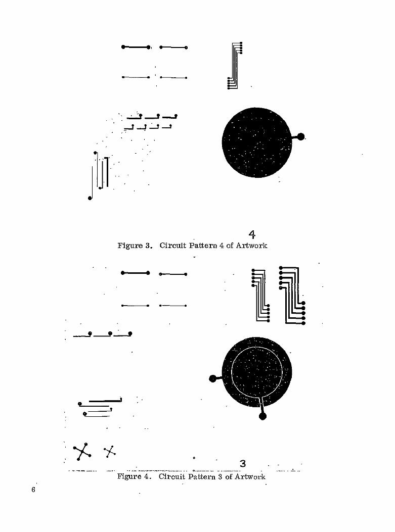