Embed Size (px)
Citation preview
© 2014 WILEY-VCH Verlag GmbH & Co. KGaA, Weinheim 1
www.advmat.dewww.MaterialsViews.com
wileyonlinelibrary.com
CO
MM
UN
ICATIO
N
Inverted Colloidal Quantum Dot Solar Cells
Gi-Hwan Kim , Bright Walker , Hak-Beom Kim , Jin Young Kim , Edward H. Sargent , * Jongnam Park , * and Jin Young Kim *
for charge carrier generation in the CQD layer drops to near-zero proximate to the metal interface. [ 16,17 ] This further reduces the amount of light that can be absorbed by the PbS layer, and limits degrees of freedom in engineering maximal absorption within a given thickness of CQD material.
To address these issues, it is attractive to architect the CQD solar cell so that more light is absorbed by an active layer of limited thickness, enabling avenues to enhanced PCE. In this work, we build a solar cell that is inverted in architecture com-pared to the standard, previously-reported, CQD photovoltaic device. This enables us to explore the introduction and engi-neering of an optical cavity for light enhancement. Specifi cally, we insert an optical spacer in a CQD photovoltaic device in order to enhance PCE by tuning the spatial distribution of the optical fi eld. [ 18,19 ]
A materials advance is pursued, achieved, and explained in the present work that is crucial to the realization of the inverted, optically-tuned, architecture. We employ a substan-tially transparent ZnO optical spacer between the photoactive CQD layer and the refl ective metal electrode in an inverted device confi guration. To do so, we develop the means to inte-grate a low-temperature, solution-processed, n-type ZnO layer as an optical spacer atop the CQD absorber. We show that the spacer offers signifi cant prospects for enhancing light absorp-tion in the CQD layer since careful choice of ZnO thickness enables judicious placement of the optical fi eld maxima within the absorber by optical simulations. Moreover, we demonstrate by experiments that the light harvesting and the photovoltaic effi ciency can be signifi cantly improved in CQD solar cells by tuning the thickness of the active layer and inserting an optical spacer between the active layer and the refl ective electrode.
As discussed herein, the new architecture offers an improve-ment in performance relative to the reference device that goes beyond optical cavity enhancement alone. We investigate using ultraviolet photoemission spectroscopy the detailed electronic structure of each of the materials incorporated into the mate-rials stack in each case. In this way, we offer experimentally-substantiated spatial band diagrams of the device that detail the origins of the enhanced voltage in the device.
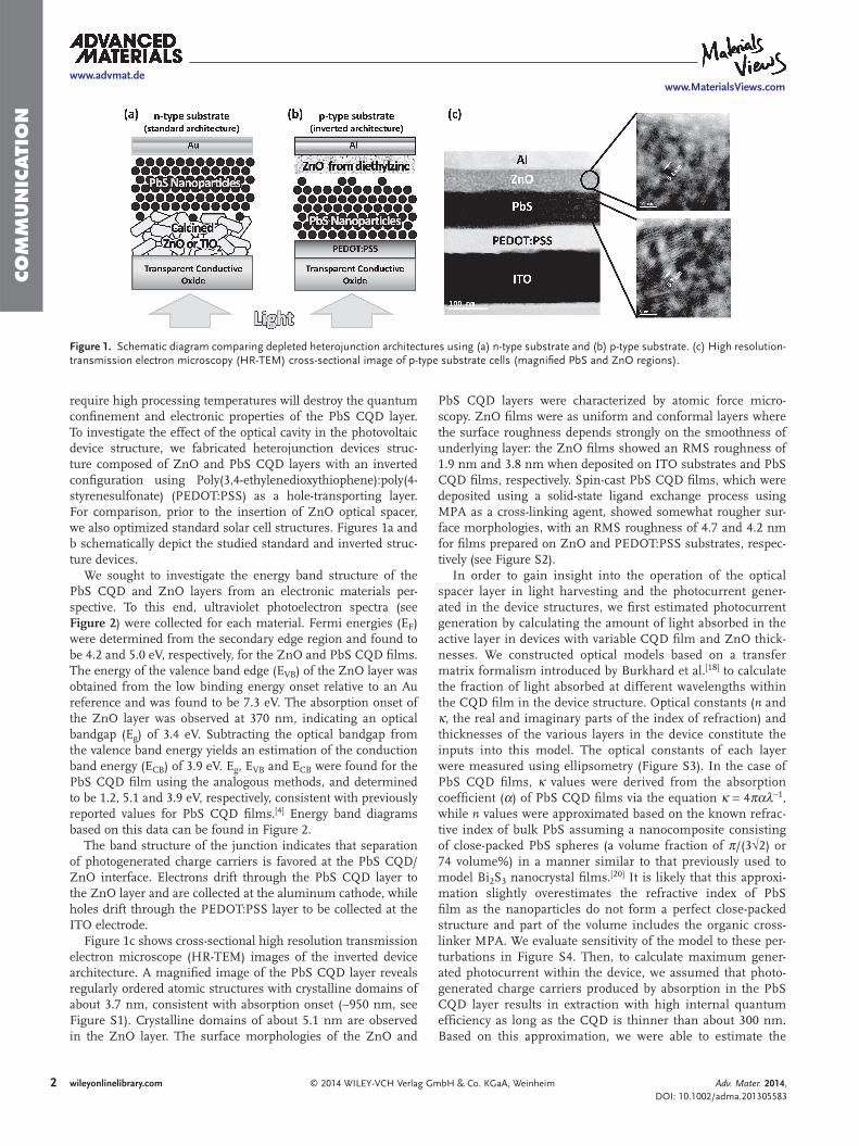
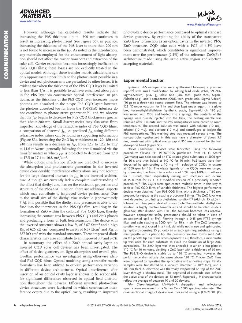
Figure 1 shows the device structures studied in this work. The devices were fabricated on indium tin oxide (ITO) coated substrates and all processing steps, except a brief immersion in a 3-mercaptopropionic acid (MPA) solution and the fi nal metal electrode deposition, were performed by spin-coating in air. The ZnO optical spacer was prepared using a diethyl zinc precursor and deposited on the CQD layer. The reactive diethyl zinc precursor decomposes rapidly to form ZnO in the presence of air and only mild thermal annealing (110 °C) is required to prepare the fi lm via this route. The low processing temperature of the ZnO layer is critical to the success of the inverted architecture; other methods of ZnO preparation which DOI: 10.1002/adma.201305583
G.-H. Kim, Dr. B. Walker, H.-B. Kim, Prof. J. Park, Prof. J. Y. Kim Interdisciplinary School of Green EnergyUlsan National Institute of Science and Technology (UNIST) Ulsan 689–798 , South Korea E-mail: [email protected]; [email protected] Dr. J. Y. Kim, Prof. E. H. Sargent Electrical and Computer EngineeringUniversity of Toronto 10 King’s College Rd , Toronto ON , Canada M5S 3G4 E-mail: [email protected] Dr. J. Y. Kim Fuel Cell Research CenterKorea Institute of Science and Technology Seoul 136-791 , South Korea
Colloidal quantum dot (CQD) solar cells have emerged as a promising class of solar cell with the potential to be manufac-tured at low cost. [ 1 ] PbS CQDs in particular are readily synthe-sized from earth-abundant elements, [ 2,3 ] and their bandgap can be conveniently and widely tuned via control over nanoparticle size. [ 4 ] Effi cient, air-stable solar cells can be fabricated under ambient conditions using solution processing techniques. [ 5 ] PbS CQDs can behave either as a p-type or n-type semicon-ductors, [ 6 ] allowing their use in a wide variety of architectures including hybrid organic/inorganic devices. [ 7 ] These materials absorb light at wavelengths of 1100 nm and beyond, offering the potential for large photocurrents compared to many widely-employed organic and inorganic materials. Additionally, CQD solar cells offer routes to effi ciencies exceeding the Shockley-Queisser limit for solar cells [ 8,9 ] via their ability to exploit mul-tiple excitons, [ 10,11 ] their promise in hot carrier extraction, [ 12 ] and their enablement of size-tuned tandem and multijunc-tion cells. Recent advances in the understanding of CQD solar cells and device fabrication have led to the demonstration of quantum effi ciencies over 100%, [ 10,11 ] and increases in certifi ed power conversion effi ciency (PCE) to 7%. [ 13–15 ]
The PCE of a CQD solar cell is directly proportional to the generated photocurrent, which is determined primarily by the fraction of incident photons absorbed in the CQD layer and by the number of extracted carriers per absorbed photon. A CQD fi lm thickness of∼1 µm is typically required to absorb all inci-dent photons, but such thick fi lms are often accompanied by insuffi cient charge transport for complete carrier extraction, limiting the optimal layer thickness to∼300 nm or less and thus reducing the amount of light absorbed by the CQD layer. Also, in the device structure widely-employed in prior CQD solar reports (here referred to as “standard”), the PbS CQD layer is located immediately adjacent the refl ective metal elec-trode. As a result, the intensity of the optical fi eld responsible
Adv. Mater. 2014, DOI: 10.1002/adma.201305583
2
www.advmat.dewww.MaterialsViews.com
wileyonlinelibrary.com © 2014 WILEY-VCH Verlag GmbH & Co. KGaA, Weinheim
CO
MM
UN
ICATI
ON
require high processing temperatures will destroy the quantum confi nement and electronic properties of the PbS CQD layer. To investigate the effect of the optical cavity in the photovoltaic device structure, we fabricated heterojunction devices struc-ture composed of ZnO and PbS CQD layers with an inverted confi guration using Poly(3,4-ethylenedioxythiophene):poly(4-styrenesulfonate) (PEDOT:PSS) as a hole-transporting layer. For comparison, prior to the insertion of ZnO optical spacer, we also optimized standard solar cell structures. Figures 1 a and b schematically depict the studied standard and inverted struc-ture devices.
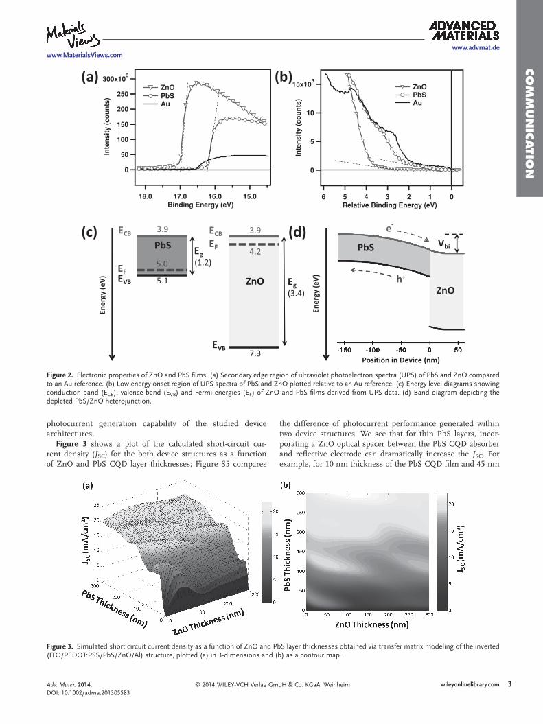
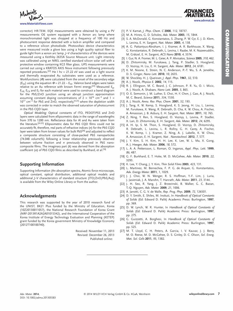
We sought to investigate the energy band structure of the PbS CQD and ZnO layers from an electronic materials per-spective. To this end, ultraviolet photoelectron spectra (see Figure 2 ) were collected for each material. Fermi energies (E F ) were determined from the secondary edge region and found to be 4.2 and 5.0 eV, respectively, for the ZnO and PbS CQD fi lms. The energy of the valence band edge (E VB ) of the ZnO layer was obtained from the low binding energy onset relative to an Au reference and was found to be 7.3 eV. The absorption onset of the ZnO layer was observed at 370 nm, indicating an optical bandgap (E g ) of 3.4 eV. Subtracting the optical bandgap from the valence band energy yields an estimation of the conduction band energy (E CB ) of 3.9 eV. E g , E VB and E CB were found for the PbS CQD fi lm using the analogous methods, and determined to be 1.2, 5.1 and 3.9 eV, respectively, consistent with previously reported values for PbS CQD fi lms. [ 4 ] Energy band diagrams based on this data can be found in Figure 2 .
The band structure of the junction indicates that separation of photogenerated charge carriers is favored at the PbS CQD/ ZnO interface. Electrons drift through the PbS CQD layer to the ZnO layer and are collected at the aluminum cathode, while holes drift through the PEDOT:PSS layer to be collected at the ITO electrode.
Figure 1 c shows cross-sectional high resolution transmission electron microscope (HR-TEM) images of the inverted device architecture. A magnifi ed image of the PbS CQD layer reveals regularly ordered atomic structures with crystalline domains of about 3.7 nm, consistent with absorption onset (∼950 nm, see Figure S1). Crystalline domains of about 5.1 nm are observed in the ZnO layer. The surface morphologies of the ZnO and
PbS CQD layers were characterized by atomic force micro-scopy. ZnO fi lms were as uniform and conformal layers where the surface roughness depends strongly on the smoothness of underlying layer: the ZnO fi lms showed an RMS roughness of 1.9 nm and 3.8 nm when deposited on ITO substrates and PbS CQD fi lms, respectively. Spin-cast PbS CQD fi lms, which were deposited using a solid-state ligand exchange process using MPA as a cross-linking agent, showed somewhat rougher sur-face morphologies, with an RMS roughness of 4.7 and 4.2 nm for fi lms prepared on ZnO and PEDOT:PSS substrates, respec-tively (see Figure S2).
In order to gain insight into the operation of the optical spacer layer in light harvesting and the photocurrent gener-ated in the device structures, we fi rst estimated photocurrent generation by calculating the amount of light absorbed in the active layer in devices with variable CQD fi lm and ZnO thick-nesses. We constructed optical models based on a transfer matrix formalism introduced by Burkhard et al. [ 18 ] to calculate the fraction of light absorbed at different wavelengths within the CQD fi lm in the device structure. Optical constants ( n and κ , the real and imaginary parts of the index of refraction) and thicknesses of the various layers in the device constitute the inputs into this model. The optical constants of each layer were measured using ellipsometry (Figure S3). In the case of PbS CQD fi lms, κ values were derived from the absorption coeffi cient ( α ) of PbS CQD fi lms via the equation κ = 4παλ −1 , while n values were approximated based on the known refrac-tive index of bulk PbS assuming a nanocomposite consisting of close-packed PbS spheres (a volume fraction of π/(3√2) or 74 volume%) in a manner similar to that previously used to model Bi 2 S 3 nanocrystal fi lms. [ 20 ] It is likely that this approxi-mation slightly overestimates the refractive index of PbS fi lm as the nanoparticles do not form a perfect close-packed structure and part of the volume includes the organic cross-linker MPA. We evaluate sensitivity of the model to these per-turbations in Figure S4. Then, to calculate maximum gener-ated photocurrent within the device, we assumed that photo-generated charge carriers produced by absorption in the PbS CQD layer results in extraction with high internal quantum effi ciency as long as the CQD is thinner than about 300 nm. Based on this approximation, we were able to estimate the
Adv. Mater. 2014, DOI: 10.1002/adma.201305583
Figure 1. Schematic diagram comparing depleted heterojunction architectures using (a) n-type substrate and (b) p-type substrate. (c) High resolution-transmission electron microscopy (HR-TEM) cross-sectional image of p-type substrate cells (magnifi ed PbS and ZnO regions).
3
www.advmat.dewww.MaterialsViews.com
wileyonlinelibrary.com© 2014 WILEY-VCH Verlag GmbH & Co. KGaA, Weinheim
CO
MM
UN
ICATIO
N
photocurrent generation capability of the studied device architectures.
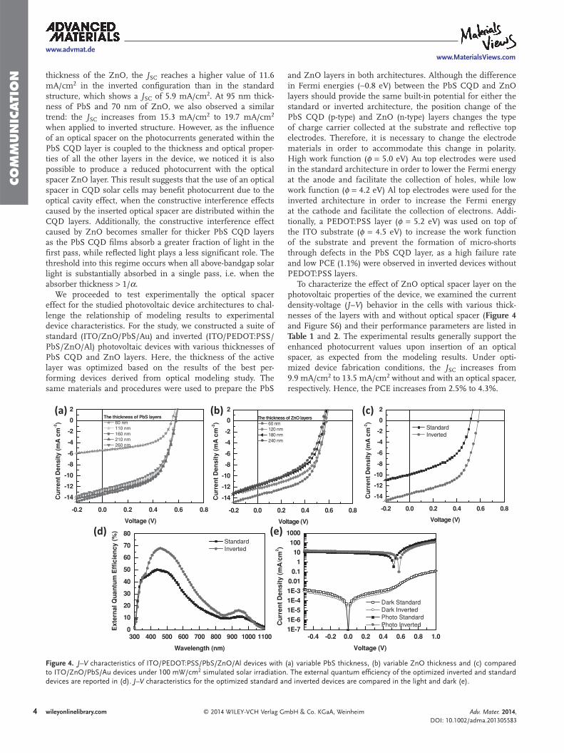
Figure 3 shows a plot of the calculated short-circuit cur-rent density ( J SC ) for the both device structures as a function of ZnO and PbS CQD layer thicknesses; Figure S5 compares
the difference of photocurrent performance generated within two device structures. We see that for thin PbS layers, incor-porating a ZnO optical spacer between the PbS CQD absorber and refl ective electrode can dramatically increase the J SC . For example, for 10 nm thickness of the PbS CQD fi lm and 45 nm
Adv. Mater. 2014, DOI: 10.1002/adma.201305583
300x103
250
200
150
100
50
0
Inte
ns
ity
(c
ou
nts
)
18.0 17.0 16.0 15.0Binding Energy (eV)
ZnO PbS Au
15x103
10
5
0
Inte
ns
ity
(c
ou
nts
)
6 5 4 3 2 1 0Relative Binding Energy (eV)
ZnO PbS Au
(b)(a)
(d)(c)
5.0
Ener
gy (e
V)
Position in Device (nm)
ECB
EFEVB
ECB
EF
3.9
5.1
PbS Eg(1.2)
EVB
3.9
4.2
7.3
ZnO
Ener
gy (e
V)
Eg(3.4)
e
h+
PbS
ZnO
Vbi
-
Figure 2. Electronic properties of ZnO and PbS fi lms. (a) Secondary edge region of ultraviolet photoelectron spectra (UPS) of PbS and ZnO compared to an Au reference. (b) Low energy onset region of UPS spectra of PbS and ZnO plotted relative to an Au reference. (c) Energy level diagrams showing conduction band (E CB ), valence band (E VB ) and Fermi energies (E F ) of ZnO and PbS fi lms derived from UPS data. (d) Band diagram depicting the depleted PbS/ZnO heterojunction.
Figure 3. Simulated short circuit current density as a function of ZnO and PbS layer thicknesses obtained via transfer matrix modeling of the inverted (ITO/PEDOT:PSS/PbS/ZnO/Al) structure, plotted (a) in 3-dimensions and (b) as a contour map.
4
www.advmat.dewww.MaterialsViews.com
wileyonlinelibrary.com © 2014 WILEY-VCH Verlag GmbH & Co. KGaA, Weinheim
CO
MM
UN
ICATI
ON thickness of the ZnO, the J SC reaches a higher value of 11.6
mA/cm 2 in the inverted confi guration than in the standard structure, which shows a J SC of 5.9 mA/cm 2 . At 95 nm thick-ness of PbS and 70 nm of ZnO, we also observed a similar trend: the J SC increases from 15.3 mA/cm 2 to 19.7 mA/cm 2 when applied to inverted structure. However, as the infl uence of an optical spacer on the photocurrents generated within the PbS CQD layer is coupled to the thickness and optical proper-ties of all the other layers in the device, we noticed it is also possible to produce a reduced photocurrent with the optical spacer ZnO layer. This result suggests that the use of an optical spacer in CQD solar cells may benefi t photocurrent due to the optical cavity effect, when the constructive interference effects caused by the inserted optical spacer are distributed within the CQD layers. Additionally, the constructive interference effect caused by ZnO becomes smaller for thicker PbS CQD layers as the PbS CQD fi lms absorb a greater fraction of light in the fi rst pass, while refl ected light plays a less signifi cant role. The threshold into this regime occurs when all above-bandgap solar light is substantially absorbed in a single pass, i.e. when the absorber thickness > 1/ α .
We proceeded to test experimentally the optical spacer effect for the studied photovoltaic device architectures to chal-lenge the relationship of modeling results to experimental device characteristics. For the study, we constructed a suite of standard (ITO/ZnO/PbS/Au) and inverted (ITO/PEDOT:PSS/PbS/ZnO/Al) photovoltaic devices with various thicknesses of PbS CQD and ZnO layers. Here, the thickness of the active layer was optimized based on the results of the best per-forming devices derived from optical modeling study. The same materials and procedures were used to prepare the PbS
and ZnO layers in both architectures. Although the difference in Fermi energies (∼0.8 eV) between the PbS CQD and ZnO layers should provide the same built-in potential for either the standard or inverted architecture, the position change of the PbS CQD (p-type) and ZnO (n-type) layers changes the type of charge carrier collected at the substrate and refl ective top electrodes. Therefore, it is necessary to change the electrode materials in order to accommodate this change in polarity. High work function (φ = 5.0 eV) Au top electrodes were used in the standard architecture in order to lower the Fermi energy at the anode and facilitate the collection of holes, while low work function (φ = 4.2 eV) Al top electrodes were used for the inverted architecture in order to increase the Fermi energy at the cathode and facilitate the collection of electrons. Addi-tionally, a PEDOT:PSS layer (φ = 5.2 eV) was used on top of the ITO substrate (φ = 4.5 eV) to increase the work function of the substrate and prevent the formation of micro-shorts through defects in the PbS CQD layer, as a high failure rate and low PCE (1.1%) were observed in inverted devices without PEDOT:PSS layers.
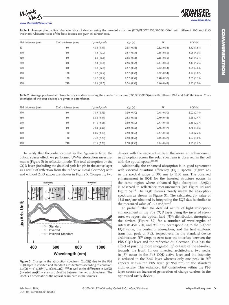
To characterize the effect of ZnO optical spacer layer on the photovoltaic properties of the device, we examined the current density-voltage ( J–V ) behavior in the cells with various thick-nesses of the layers with and without optical spacer ( Figure 4 and Figure S6) and their performance parameters are listed in Table 1 and 2 . The experimental results generally support the enhanced photocurrent values upon insertion of an optical spacer, as expected from the modeling results. Under opti-mized device fabrication conditions, the J SC increases from 9.9 mA/cm 2 to 13.5 mA/cm 2 without and with an optical spacer, respectively. Hence, the PCE increases from 2.5% to 4.3%.
Adv. Mater. 2014, DOI: 10.1002/adma.201305583
-0.2 0.0 0.2 0.4 0.6 0.8
-14
-12
-10
-8
-6
-4
-2
0
2
Cu
rre
nt
De
ns
ity (
mA
cm
-2)
Voltage (V)
The thickness of ZnO layers 60 nm 120 nm 180 nm 240 nm
-0.2 0.0 0.2 0.4 0.6 0.8
-14
-12
-10
-8
-6
-4
-2
0
2
Cu
rre
nt
De
ns
ity
(m
A c
m-2)
Voltage (V)
Standard Inverted
-0.2 0.0 0.2 0.4 0.6 0.8
-14
-12
-10
-8
-6
-4
-2
0
2
Cu
rre
nt
De
nsit
y (
mA
cm
-2)
Voltage (V)
The thickness of PbS layers 60 nm 110 nm 160 nm 210 nm 260 nm
300 400 500 600 700 800 900 1000 11000
10
20
30
40
50
60
70
80
Exte
rnal Q
ua
ntu
m E
ffic
ien
cy (
%)
Wavelength (nm)
Standard Inverted
-0.4 -0.2 0.0 0.2 0.4 0.6 0.8 1.01E-7
1E-6
1E-5
1E-4
1E-3
0.01
0.1
1
10
100
1000
Cu
rre
nt
De
nsit
y (
mA
/cm
2)
Voltage (V)
Dark Standard Dark Inverted Photo Standard Photo Inverted
(a) (b)
(d) (e)
(c)
Figure 4. J–V characteristics of ITO/PEDOT:PSS/PbS/ZnO/Al devices with (a) variable PbS thickness, (b) variable ZnO thickness and (c) compared to ITO/ZnO/PbS/Au devices under 100 mW/cm 2 simulated solar irradiation. The external quantum effi ciency of the optimized inverted and standard devices are reported in (d). J–V characteristics for the optimized standard and inverted devices are compared in the light and dark (e).
5
www.advmat.dewww.MaterialsViews.com
wileyonlinelibrary.com© 2014 WILEY-VCH Verlag GmbH & Co. KGaA, Weinheim
CO
MM
UN
ICATIO
N
To verify that the enhancement in the J SC arises from the optical spacer effect, we performed UV-Vis absorption measure-ments ( Figure 5 ) in refl ection mode. The total absorption by the CQD layer (including the doubled path length in the active layer as a result of refl ection from the refl ective metal electrode) with and without ZnO spacer are shown in Figure 5 . Comparing two
devices with the same active layer thickness, an enhancement in absorption across the solar spectrum is observed in the cell with the optical spacer. [ 16,19 ]
Additionally, the enhanced absorption is in good agreement with external quantum effi ciency (EQE) spectra (Figure 4 d) in the spectral range of 300 nm to 1100 nm. The observed enhancement in EQE for the inverted structure occurs in the same region where enhanced light absorption ( Δα ( Ω )) is observed in refl ectance measurements (see Figure 4 d and Figure 5 ). [ 16 ] The EQE features closely match the absorption spectrum as shown in Figure S1. The calculated J SC value of 13.8 mA/cm 2 obtained by integrating the EQE data is similar to the measured value of 13.5 mA/cm 2 .
To probe further the detailed nature of light absorption enhancement in the PbS CQD layer using the inverted struc-ture, we report the optical fi eld ( |E| 2 ) distribution throughout the devices (Figure S7) for a number of wavelengths of interest: 450, 700, and 950 nm, corresponding to the highest EQE value, the center of absorption, and the fi rst excitonic transition peak of PbS, respectively. In the standard device architecture, |E| 2 drops to zero near the interface between the PbS CQD layer and the refl ective Au electrode. This has the effect of pushing more integrated |E| 2 outside of the absorber, towards the front. In our inverted architecture, two peaks in |E| 2 occur in the PbS CQD active layer and the intensity is reduced in the ZnO layer whereas only one peak in |E| 2 appears within the PbS layer (at 950 nm) in the standard architecture. This enhanced |E| 2 distribution within the PbS layer causes an increased generation of charge carriers in the optimized cavity device.
Adv. Mater. 2014, DOI: 10.1002/adma.201305583
Table 1. Average photovoltaic characteristics of devices using the inverted structure (ITO/PEDOT:PSS/PbS/ZnO/Al) with different PbS and ZnO thickness. Characteristics of the best devices are given in parentheses.
PbS thickness (nm) ZnO thickness (nm) J SC (mA/cm 2 ) V OC (V) FF PCE (%)
60 60 4.85 (5.41) 0.55 (0.55) 0.52 (0.54) 1.42 (1.61)
110 60 11.4 (12.7) 0.57 (0.57) 0.55 (0.56) 3.95 (4.05)
160 60 12.9 (13.5) 0.58 (0.58) 0.55 (0.55) 4.21 (4.31)
210 60 12.3 (13.1) 0.58 (0.58) 0.54 (0.56) 4.13 (4.25)
260 60 11.2 (12.5) 0.57 (0.58) 0.52 (0.53) 3.69 (3.84)
160 120 11.2 (12.2) 0.57 (0.58) 0.52 (0.54) 3.74 (3.82)
160 180 11.2 (11.7) 0.57 (0.57) 0.48 (0.50) 3.05 (3.33)
160 240 10.5 (11.6) 0.54 (0.55) 0.46 (0.48) 2.85 (3.06)
Table 2. Average photovoltaic characteristics of devices using the standard structure (ITO/ZnO/PbS/Au) with different PbS and ZnO thickness. Char-acteristics of the best devices are given in parentheses.
PbS thickness (nm) ZnO thickness (nm) J SC (mA/cm 2 ) V OC (V) FF PCE (%)
110 60 7.89 (8.55) 0.50 (0.50) 0.48 (0.50) 2.02 (2.14)
160 60 8.85 (9.91) 0.52 (0.52) 0.49 (0.48) 2.25 (2.47)
210 60 9.15 (9.68) 0.50 (0.50) 0.47 (0.49) 2.15 (2.37)
260 60 7.68 (8.03) 0.50 (0.52) 0.46 (0.47) 1.75 (1.96)
160 120 8.85 (9.13) 0.50 (0.50) 0.47 (0.49) 2.06 (2.24)
160 180 7.42 (7.73) 0.50 (0.52) 0.45 (0.47) 1.67 (1.89)
160 240 7.15 (7.70) 0.50 (0.50) 0.44 (0.46) 1.55 (1.77)
400 600 800 1000
ΔΔ ΔΔ α
α α α (( (( A
rb. U
nit )) ))
Wavelength (nm)
Standard Inverted Inverted-Standard
ITO
/G
lass
PED
OT
ZnO A
l
ITO
/G
lass
PED
OT
ZnO A
l
PbS
Iin
Iout
Iin'
Iout'
ITO
/G
lass
ZnO Au
ITO
/G
lass
ZnO Au
PbS
Iin
Iout
Iin'
Iout'
Standard Inverted
Figure 5. Change in the absorption spectrum ( Δα ( Ω )) due to the PbS CQD layer in inverted and standard architectures according to equation: Δα ( Ω ) = −(1 d /2) ln ( I’ out ( Ω )/ I out ( Ω )), [ 16 ] as well as the difference in Δα ( Ω ) (inverted Δα ( Ω ) – standard Δα ( Ω )) between the two architectures. The inset is a schematic of the optical beam path in the samples.
6
www.advmat.dewww.MaterialsViews.com
wileyonlinelibrary.com © 2014 WILEY-VCH Verlag GmbH & Co. KGaA, Weinheim
CO
MM
UN
ICATI
ON
Adv. Mater. 2014, DOI: 10.1002/adma.201305583
However, although the calculated results indicate that increasing the PbS thickness up to ∼500 nm continues to result in increasing photocurrent (see Figure S5), in practice, increasing the thickness of the PbS layer to more than 200 nm is not found to increase in the J SC . As noted in the introduction, any materials employed for the enhancement of light absorp-tion should not affect the carrier transport and extraction of the solar cell. Carrier extraction becomes increasingly ineffi cient in thick CQD fi lms; these losses are not explicitly treated in the optical model. Although these transfer matrix calculations can only approximate upper limits to the photocurrent possible in a device and real photocurrents are perturbed by other losses, it is evident that when the thickness of the PbS CQD layer is limited to less than 1/ α it is possible to achieve enhanced absorption in the PbS layer via constructive optical interference. In par-ticular, as the thickness of the PbS CQD layer increases, more photons are absorbed in the p-type PbS CQD layer; however, the photons absorbed too far from the PbS/ZnO interface do not contribute to photocurrent generation, [ 21 ] and we observe that the J SC begins to decrease for PbS CQD thicknesses greater than about 200 nm. Small discrepancies may also arise from imperfect knowledge of the refractive index of PbS CQD fi lms; a comparison of observed J SC vs. predicted J SC using different refractive index values can be found in supporting information (Figure S3). Increasing the ZnO layer thickness to 120, 180 and 240 nm results in a decrease in J SC , from 12.7 to 12.2 to 11.7 to 11.6 mA/cm 2 , generally following the trend modeled via the transfer matrix in which J SC is predicted to decrease from 17.9 to 17.5 to 17.4 to 16.8 mA/cm 2 .
While optical interference effects are predicted to increase the absorption and photocurrent generation in the inverted device considerably, interference effects alone may not account for the large observed increase in J SC in the inverted architec-ture. Although we currently lack a complete understanding of the effect that diethyl zinc has on the electronic properties and structure of the PbS/ZnO junction, there are additional aspects which may contribute to improved device performance. Due to the small size of the diethyl zinc molecule (approximately 7 Å), it is possible that the diethyl zinc precursor is able to dif-fuse into the interstices in the PbS QD fi lm, resulting in the formation of ZnO within the colloidal PbS CQD layer, thereby increasing the contact area between PbS CQD and ZnO phases and producing a form of bulk heterojunction. The device with the inverted structure shows a low R S of 2.67 Ωcm 2 and a high R Sh of 626 kΩ cm 2 compared to an R S of 6.37 Ωcm 2 and R Sh of 387 kΩ cm 2 with the standard structure. These improved diode characteristics may also contribute to an improved FF and PCE .
In summary, the effect of a ZnO optical cavity layer on inverted CQD solar cell devices has been investigated. The effect of device geometry on light absorption and overall pho-tovoltaic performance was investigated using otherwise iden-tical PbS CQD fi lms. Optical modeling using a transfer matrix formalism has been utilized to explain performance variation in different device architectures. Optical interference after insertion of an optical cavity layer is shown to be responsible for signifi cant differences observed in optical fi eld distribu-tion throughout the devices. Effi cient inverted photovoltaic device structures were fabricated in which constructive inter-ference occurs due to the optical cavity, resulting in improved
photovoltaic device performance compared to optimal standard device geometry. By exploiting the ability of the transparent ZnO layer to function as an optical cavity in the inverted PbS/ZnO structure, CQD solar cells with a PCE of 4.3% have been demonstrated, which constitutes a signifi cant improve-ment over the performance (2.5%) of the reference ZnO/PbS architecture made using the same active region and electron accepting materials.
Experimental Section Synthesis : PbS nanoparticles were synthesized following a previous
report [ 4 ] with small modifi cation by adding lead oxide (PbO, 99.99%, Sigma-Aldrich) (0.47 g), oleic acid (OA, tech. grade 90%, Sigma-Aldrich) (2 g), and 1-octadecene (ODE, tech. grade 90%, Sigma-Aldrich) (10 g) to a three-neck round bottom fl ask. The mixture was heated to 125 °C under vacuum for 1 hr and then kept under argon. In a glove box, hexamethyldisilathiane (synthetic grade, Sigma-Aldrich, 180 µL) was mixed with ODE and loaded into a syringe. The contents of the syringe were quickly injected into the fl ask, the heating mantle was removed after 1 minute and the PbS nanoparticles were cooled to room temperature. The reacted solution was mixed with toluene (10 mL), ethanol (10 mL), and acetone (10 mL) and centrifuged to isolate the PbS nanoparticles. This washing step was repeated several times. The nanoparticles synthesized in this way have a diameter of about 3.7 nm, consistent with optical energy gap at 950 nm observed for the fi rst absorption band (Figure S1).
Device Fabrication: Devices were fabricated using the following procedure: Clevios PH PEDOT:PSS purchased from H. C. Starck (Germany) was spin-coated on ITO coated glass substrates at 5000 rpm for 60 s and then baked at 140 °C for 10 min. PbS layers were then deposited by spin-coating a 10 mg ml −1 solution of CQDs in octane at 1500 rpm for 15s. The oleate ligands of the CQDs were exchanged by immersing the fi lms into a solution of 10% (v/v) MPA in methanol for 1 minute, then sequentially rinsing with methanol and octane at 1500 rpm for 15 s in a modifi ed version of a previously reported procedure. [ 4 ] PbS CQDs were spin-coated multiple times in this way to achieve PbS CQD fi lms of variable thickness. The highest performance devices were obtained from PbS CQD fi lms with a thickness of 160 nm, prepared by repeating the coating procedure 8 times. The ZnO layer was next deposited by diluting a diethylzinc solution [ 27 ] (Aldrich, 15 wt.% in toluene) with two parts tetrahydrofuran (note: the un-diluted diethyl zinc solution is highly reactive towards air and should be handled inside a glovebox; after dilution with THF, the solution becomes less reactive, however, appropriate safety precautions should be taken in case of an accidental spill or fi re), fi ltering through a 0.45 µm PTFE syringe fi lter and spin coating at 3000 rpm for 30 s in air. The ZnO precursor solution was kept closed in a 4 mL vial while not in use and spin-coated by rapidly dispensing 25 µL onto an already spinning substrate using a micropipette with a plastic tip. The precursor solution forms solid ZnO on the pipette tip over time when exposed to air, therefore, a new plastic tip was used for each substrate to avoid the formation of large ZnO particulates. The ZnO layer was then annealed in air on a hot plate at 110 °C for 10 minutes, yielding a ZnO layer with a thickness of 60 nm. The PbS/ZnO device is stable up to 120 °C annealing, however, the performance dramatically decreases above 120 °C. Thicker ZnO fi lms were prepared by repeating the spincoating and annealing steps. Finally, samples were transferred to a vacuum chamber (< 10 −6 torr), and a 100 nm thick Al electrode was thermally evaporated on top of the ZnO layer through a shadow mask. The deposited Al electrode area defi ned the active area of the devices as 13 mm 2 . Reported J–V characteristics refl ect the average of between 10 and 20 devices.
Film Characterization: UV-Vis-NIR absorption and refl ectance spectra were measured on a Varian Cary 5000 spectrophotometer. The cross-sectional image of device was measured using a JEM-2100F (Cs
7
www.advmat.dewww.MaterialsViews.com
wileyonlinelibrary.com© 2014 WILEY-VCH Verlag GmbH & Co. KGaA, Weinheim
CO
MM
UN
ICATIO
N
corrector) HR-TEM. EQE measurements were obtained by using a PV measurements OE system equipped with a Xenon arc lamp where monochromated light was chopped at a frequency of 100 Hz and photocurrent response detected with a lock-in amplifi er and compared to a reference silicon photodiode. Photovoltaic device characteristics were measured inside a glove box using a high quality optical fi ber to guide light from a xenon arc lamp. J–V characteristics of the devices were measured using a Keithley 2635A Source Measure unit. Light intensity was calibrated using an NREL certifi ed standard silicon solar cell with a protective window containing KG5 fi lter glass. UPS measurements were carried out using a KRATOS AXIS Nova instrument following previously reported procedures. [ 22 ] He I hv = 21.22 eV was used as a light source and thermally evaporated Au substrates were used as a reference. Workfunctions (Φ) were calculated from the onset of the secondary edge (E SE ) using the equation Φ = 21.22 – E SE . Valence band edges were taken relative to an Au reference with known Fermi energy. [ 22 ] Measured E g , E VB, E CB and E F for each material were used to construct a band diagram for the PbS/ZnO junction using an abrupt junction approximation assuming constant doping concentrations of 2 × 10 16 cm −3 and 1 × 10 17 cm −3 for PbS and ZnO, respectively, [ 4,23 ] where the depletion width was corrected in order to match the observed saturation of photocurrent in the PbS CQD layer.
Optical Modeling: Optical constants of ITO, PEDOT:PSS and ZnO layers were calculated from ellipsometric data in the range of wavelengths from 370 to 1200 nm. Refl ectance data for Al and Au were taken from the literature. [ 24,25 ] Ellipsometric data for PbS CQD fi lms could not be accurately fi t, therefore, real parts of refractive indices ( n ) for the PbS CQD layer were taken from known values for bulk PbS [ 26 ] and adjusted to refl ect a composite structure consisting of close-packed PbS nanoparticles (74.048 volume%) following a linear relationship previously observed between volume fraction and n previously observed in PbS nano-composite fi lms. The imaginary part ( k ) was derived from the absorption coeffi cient (α) of PbS CQD fi lms as described by Burkhard, et al. [ 18 ]
Supporting Information Supporting Information (An absorption spectra, Atomic force microscope, optical constant, optical distribution, additional optical models and additional J–V characteristics of standard structure (ITO/ZnO/PbS/Au)) is available from the Wiley Online Library or from the author.
Acknowledgements This research was supported by the year of 2010 research fund of the UNIST, BK21 Plus funded by the Ministry of Education, Korea (10Z20130011057), the National Research Foundation of Korea Grant (NRF-2013R1A2A2A01015342), and the International Cooperation of the Korea Institute of Energy Technology Evaluation and Planning (KETEP) grant funded by the Korea government Ministry of Knowledge Economy (2012T100100740).
[1] P. V. Kamat , J. Phys. Chem. C 2008 , 112 , 18737 . [2] M. A. Hines , G. D. Scholes , Adv. Mater. 2003 , 15 , 1844 . [3] S. A. McDonald , G. Konstantatos , S. Zhang , P. W. Cyr , E. J. D. Klem ,
L. Levina , E. H. Sargent , Nat. Mater. 2005 , 4 , 138 . [4] A. G. Pattantyus-Abraham , I. J. Kramer , A. R. Barkhouse , X. Wang ,
G. Konstantatos , R. Debnath , L. Levina , I. Raabe , M. K. Nazeeruddin , M. Grätzel , E. H. Sargent , ACS Nano 2010 , 4 , 3374 .
[5] I. Gur , N. A. Fromer , M. L. Geier , A. P. Alivisatos , Science 2005 , 310 , 462 . [6] D. Zhitomirsky , M. Furukawa , J. Tang , P. Stadler , S. Hoogland ,
O. Voznyy , H. Liu , E. H. Sargent , Adv. Mater. 2012 , 24 , 6181 . [7] K. M. Noone , E. Strein , N. C. Anderson , P.-T. Wu , S. A. Jenekhe ,
D. S. Ginger , Nano Lett. 2010 , 10 , 2635 . [8] W. Shockley , H. J. Queisser , J. Appl. Phys. 1961 , 32 , 510 . [9] A. J. Nozik , Physica E. 2002 , 14 , 115 .
[10] R. J. Ellingson , M. C. Beard , J. C. Johnson , P. R. Yu , O. I. Micic , A. J. Nozik , A. Shabaev , Nano Lett. 2005 , 5 , 865 .
[11] O. E. Semonin , J. M. Luther , S. Choi , H.-Y. Chen , J. Gao , A. J. Nozik , M. C. Beard , Science 2011 , 334 , 1530 .
[12] A. J. Nozik , Annu. Rev. Phys. Chem. 2001 , 52 , 193 . [13] J. Tang , K. W. Kemp , S. Hoogland , K. S. Jeong , H. Liu , L. Levina ,
M. Furukawa , X. Wang , R. Debnath , D. Cha , K. W. Chou , A. Fischer , A. Amassian , J. B. Asbury , E. H. Sargent , Nat. Mater. 2011 , 10 , 765 .
[14] Z. Ning , Y. Ren , S. Hoogland , O. Voznyy , L. Levina , P. Stadler , X. Lan , D. Zhitomirsky , E. H. Sargent , Adv. Mater. 2012 , 24 , 6295 .
[15] A. H. Ip , S. M. Thon , S. Hoogland , O. Voznyy , D. Zhitomirsky , R. Debnath , L. Levina , L. R. Rollny , G. H. Carey , A. Fischer , K. W. Kemp , I. J. Kramer , Z. Ning , A. J. Labelle , K. W. Chou , A. Amassian , E. H. Sargent , Nat . Nanotechnol. 2012 , 7 , 577 .
[16] J. Y. Kim , S. H. Kim , H. H. Lee , K. Lee , W. L. Ma , X. Gong , A. J. Heeger , Adv. Mater. 2006 , 18 , 572 .
[17] L. A. A. Pettersson , L. Roman , O. Inganas , Appl. Phys. Lett. 1999 , 86 , 487 .
[18] G. F. Burkhard , E. T. Hoke , M. D. McGehee , Adv. Mater. 2010 , 22 , 3293 .
[19] K. Lee , Y. Chang , J. Y. Kim , Thin Solid Films 2003 , 423 , 131 . [20] L. Martinez , M. Bernechea , F. P. G. de Arquer , G. Konstantatos ,
Adv. Energy Mater. 2011 , 1 , 1029 . [21] J. J. Choi , W. N. Wenger , R. S. Hoffman , Y.-F. Lim , J. Luria ,
J. Jasieniak , J. A. Marohn , T. Hanrath , Adv. Mater. 2011 , 23 , 3144 . [22] J. H. Seo , R. Yang , J. Z. Brzezinski , B. Walker , G. C. Bazan ,
T.-Q. Nguyen , Adv. Mater. 2009 , 21 , 1006 . [23] A. Janotti , C. G. V. de Walle , Rep. Prog. Phys. 2009 , 72 , 126501 . [24] D. Y. Smith , E. Shiles , M. Inokuti , In Handbook of Optical Constants
of Solids (Ed: Edward D. Palik ) Academic Press : Burlington , 1997 , pp. 369 .
[25] D. W. Lynch , W. R. Hunter , In Handbook of Optical Constants of Solids (Ed: Edward D. Palik) Academic Press : Burlington , 1997 , pp. 275 .
[26] G. Guizzetti , A. Borghesi , In Handbook of Optical Constants of Solids (Ed: Edward D. Palik) Academic Press : Burlington , 1997 , pp. 525 .
[27] M. T. Lloyd , C. H. Peters, A. Garcia, I. V. Kauvar, J. J. Berry, M. O. Reese, M. D. McGehee, D. S. Ginley, D. C. Olson , Sol. Energ. Mat. Sol. Cells 2011 , 95 , 1382.
Received: November 11, 2013 Revised: December 26, 2013
Published online:
Adv. Mater. 2014, DOI: 10.1002/adma.201305583