Embed Size (px)
Citation preview
Supplumental data items
Colloidal Quantum Dot Photodetectors with 10 ns response time and 80% Quantum
Efficiency at 1550 nm
Maral Vafaie1, James Z. Fan1, Amin Morteza Najarian1, Olivier Ouellette2, Laxmi Kishore
Sagar1, Koen Bertens1, Bin Sun1, F. Pelayo García de Arquer1 and Edward H. Sargent1*
1Department of Electrical and Computer Engineering, University of Toronto, 10 King’s
College Road, Toronto, Ontario, M5S 3G4, Canada 2Laboratory for Photonics and Interfaces, École Polytechnique Fédérale de Lausanne, CH
1015 Lausanne, Switzerland
*Correspondence: [email protected]
Figure S1. TEM images of the as-synthesized oleic acid capped PbS quantum dots
used in this study.
TEM magnification is shown with a scale bar of a) 10 nm and b) 5nm. The mean size
of the dots equals 5.7±0.4 nm giving rise to the estimated band gap of 0.81 eV. 1
Figure S2. SEM image of a QD film undergone LLB only strategy.
SEM images are show with magnification of Magnification of a) 1.5k and b) 10k. Degraded
colloidal stability of this ligand exchange route leads to macroscopically agglomerated
structures.
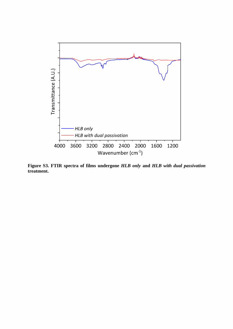
Figure S3. FTIR spectra of films undergone HLB only and HLB with dual passivation
treatment.
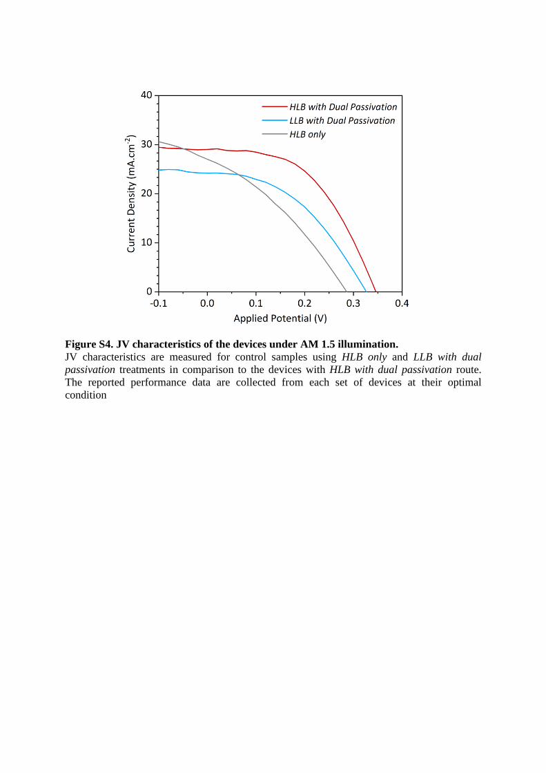
Figure S4. JV characteristics of the devices under AM 1.5 illumination.
JV characteristics are measured for control samples using HLB only and LLB with dual
passivation treatments in comparison to the devices with HLB with dual passivation route.
The reported performance data are collected from each set of devices at their optimal
condition

Table S1. photodiode parameters extracted from J-V characterization under
illumination with simulated AM1.5G.
Average values and standard deviation of photodiode parameters extracted from J-V
characterization under illumination with simulated AM1.5G for minimum sample size of 10.
Representative J-V characteristics are shown in Figure S4.
Sample ID Voc (V) Jsc (mA.cm-2) FF (%)
HLB with Dual Passivation 0.34±0.01 29.5±1.4 41±0.06
LLB with Dual Passivation 0.33±0.02 27.5±2.1 38.5±0.04
HLB only 0.32±0.02 26.4±1.3 28±0.03
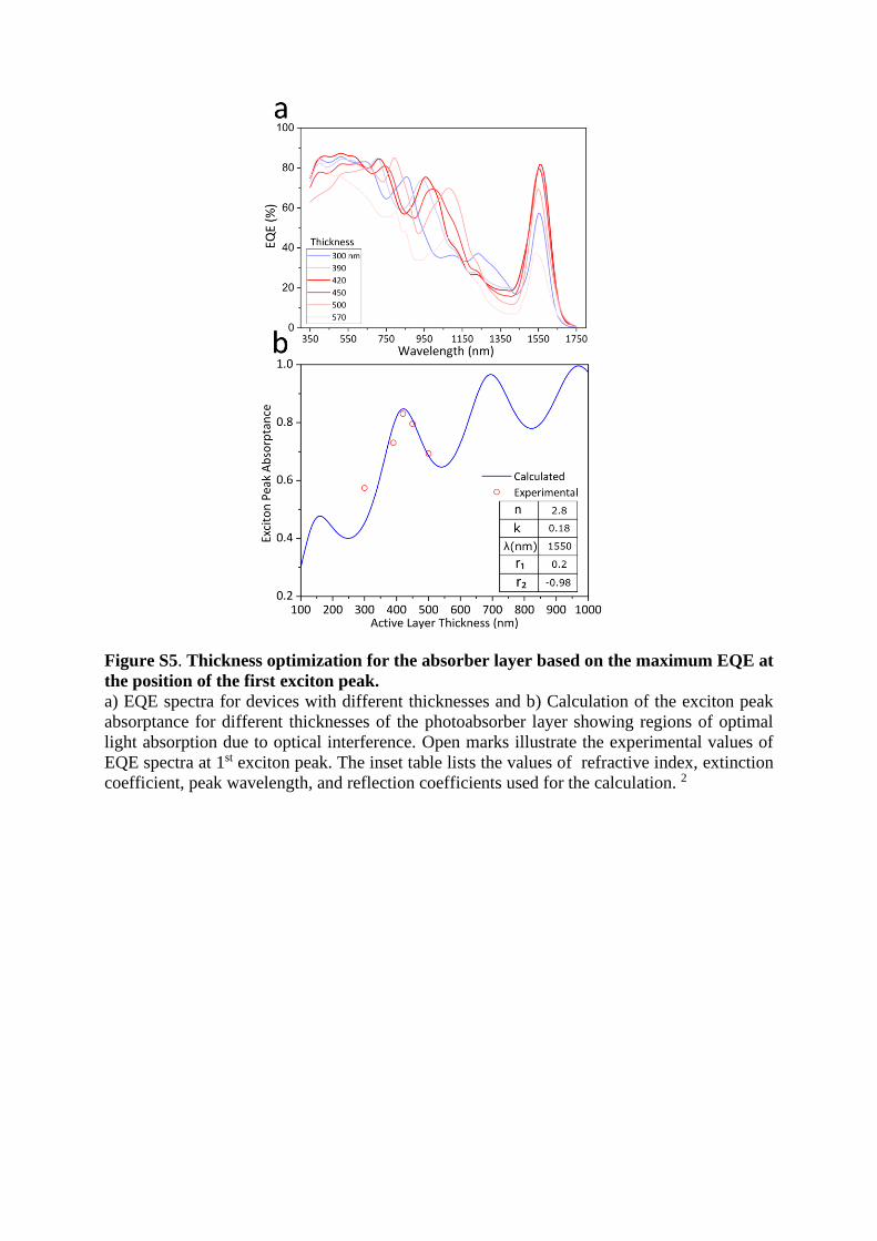
Figure S5. Thickness optimization for the absorber layer based on the maximum EQE at
the position of the first exciton peak.
a) EQE spectra for devices with different thicknesses and b) Calculation of the exciton peak
absorptance for different thicknesses of the photoabsorber layer showing regions of optimal
light absorption due to optical interference. Open marks illustrate the experimental values of
EQE spectra at 1st exciton peak. The inset table lists the values of refractive index, extinction
coefficient, peak wavelength, and reflection coefficients used for the calculation. 2
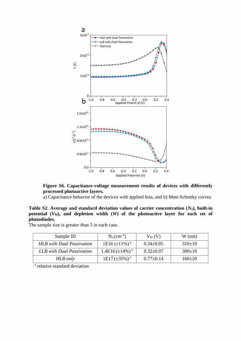
Figure S6. Capacitance-voltage measurement results of devices with differently
processed photoactive layers.
a) Capacitance behavior of the devices with applied bias, and b) Mott-Schottky curves.
Table S2. Average and standard deviation values of carrier concentration (Na), built-in
potential (Vbi), and depletion width (W) of the photoactive layer for each set of
photodiodes.
The sample size is greater than 5 in each case.
Sample ID Na (cm-3) Vbi (V) W (nm)
HLB with Dual Passivation 1E16 (±11%) a 0.34±0.05 310±10
LLB with Dual Passivation 1.4E16 (±14%) a 0.32±0.07 300±10
HLB only 1E17 (±35%) a 0.77±0.14 160±20
a relative standard deviation

Figure S7. Capacitance vs. frequency behavior of our photodetector using the
impedance spectroscopy method.
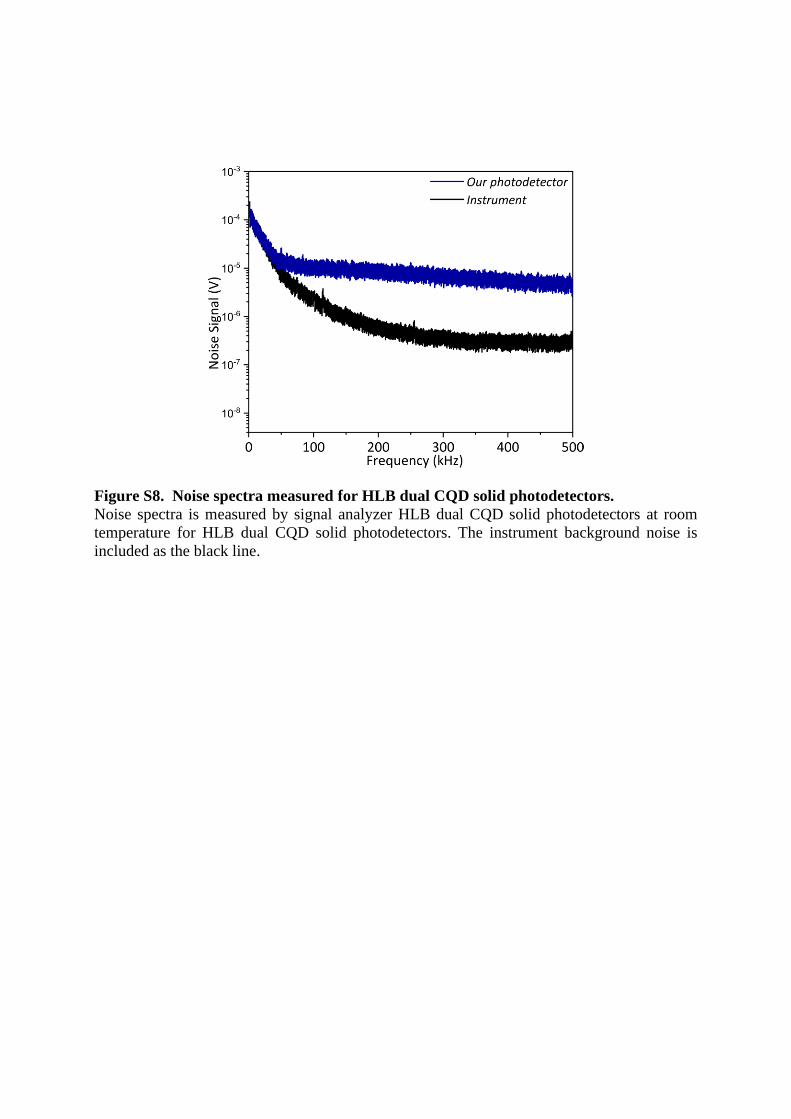
Figure S8. Noise spectra measured for HLB dual CQD solid photodetectors.
Noise spectra is measured by signal analyzer HLB dual CQD solid photodetectors at room
temperature for HLB dual CQD solid photodetectors. The instrument background noise is
included as the black line.

Table S3. Response time values for each pixel size in photodetectors fabricated via HLB
with dual passivation exchange route.
Average values and standard deviation of response time for each pixel size in photodetectors
fabricated via HLB with dual passivation exchange route. The fall time is defined by the
interval between 10% to 90% of peak amplitude. The sample size is greater than 10 in each
case.
Sample ID HLB with Dual Passivation
Pixel Diameter (μm) 100 200 500 1000 1400
Fall time (ns) 9.8±0.5 32±13 400±100 1000±70 1500±100
Figure S9. Measured and estimated time response as a function of pixel area.
The estimated values are obtained assuming a parallel plane capacitor model.
Table S4. Response time values for each pixel size in photodetectors treated with control
exchange routes.
Average values and standard deviation of response time for each pixel size in photodetectors
treated with control exchange routes. The fall time is defined by the interval between 10% to
90% of peak amplitude. The sample size is greater than 10 in each case.
Sample ID LLB with Dual Passivation
Pixel Diameter (μm) 100 200 500 1000 1400
Fall time (ns) 9.8±0.4 40±34 500±200 700±300 1400±200
Sample ID HLB only
Fall time (ns) 10.3±0.6 50±11 700±100 900±70 1500±200
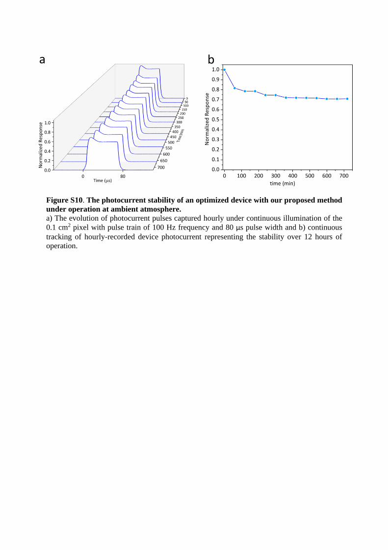
Figure S10. The photocurrent stability of an optimized device with our proposed method
under operation at ambient atmosphere.
a) The evolution of photocurrent pulses captured hourly under continuous illumination of the
0.1 cm2 pixel with pulse train of 100 Hz frequency and 80 μs pulse width and b) continuous
tracking of hourly-recorded device photocurrent representing the stability over 12 hours of
operation.
Supplemental Experimental Procedures
Thickness optimization for the absorber layer
We sought to find the optimal value for the thickness of the absorber layer in order to have the
highest photosensitivity at wavelength of 1550 nm. For this purpose, different concentrations
of CQD ink were prepared and spin coated to prepare devices. The EQE spectrum of each
device is illustrated in Figure S5a. To confirm this optimization, the active layer absorptance
at the wavelength matching that of the first exciton peak was calculated (Figure S5b) using a
simplified Fabry-Perot model and estimated values for the refractive indices of the CQD film
and the optical cavity from previous work.2 Light absorption at the exciton peak is maximized
at active layer thickness near 420 nm, in agreement with our experimental findings. Due to
destructive interference, further improvements in light absorption are expected only for active
layer thicknesses beyond 650 nm. For such thick active layers, incomplete photocarrier
extraction causes a severe drop in internal quantum efficiency which in turn reduces EQE, as
is the case for the 570 nm-thick device.
Capacitance-voltage spectroscopy
Capacitance (C) was measured as a function of DC bias from -1 to 1 V with a 10 kHz, 50 mV
rms, AC signal in the absence of illumination. We extracted the carrier concentration (Na),
built-in potential (Vbi), and depletion width (W) of the photoactive layer employing the Mott-
Schottky relation in the linear part of 1/C2 as follows: 3
where ε is the relative dielectric constant of the PbS QD (calculated to be equal to 34 based on
impedance spectroscopy measurements detailed below), and Nd is the carrier concentration of
the donors in electron transport layer (ZnO). We assumed an Nd = 1E+18 cm-3 and a device
area (A) of 0.1 cm2. The obtained capacitance-voltage traces as well as the parameters for
each device set are respectively shown in Figure S6 and Table S2. The value of the ε is
estimated based on by impedance spectroscopy. The optimized device was connected to
Autolab Potentiostat/Galvanostat module with an applied AC voltage perturbation of 20 mV
while the device is kept at dark and short-circuit condition. The impedance spectra are
collected for the frequency in the range of 1 Hz to 1 MHz. The capacitance component C is
plotted in Figure S7. The capacitance value in the plateau located in high-frequency regime
(105 to 106 Hz) represents the geometrical capacitance corresponding to the dielectric
response of the photoactive layer. Accordingly, the dielectric constant of the PbS QD layer
corresponds to ~34 based on the parallel capacitance assumption where the capacitance,
device area, and active layer thickness were set to 7.54E-8 (F.cm-2), 0.1 cm2, and 400 nm.
Response time studies
Based on the Measurement of transient photoresponse for pixels with different sizes within
the same device (Figure 4c), we were able to analyze the effect of pixel area on the response
time of our detectors. Table S3 provides the average and standard deviation values of the
response time for each pixel size of our optimized photodetector. The analysis suggests that

even at the smallest pixel area, the time response is limited by the geometrical capacitance.
Using a dielectric constant of 34, as calculated from impedance spectroscopy measurements
(capacitance-voltage spectroscopy section of this document), the area of each pixel, an active
layer thickness of 400 nm as measured using profilometer, and under the assumption of
parallel plate capacitance, we estimate the time decay from RC-limited time response formula
represented by 2.2RC where R corresponds to 50 Ω load input of the oscilloscope. The
estimated and measured response time values are shown in Figure S9. The two sets of data
follow the same linear behavior with the same slope in the log-log scale, which supports the
dominant effect of capacitance as a limiting factor of device speed. The fixed offset for all the
data points suggesting the potential presence of another capacitance source in the system. This
notion can be more considered when the values of response time for control devices are
measured (Table S4) and compared to the optimized devices. No significant difference is seen
in the mentioned values even though each set of devices have demonstrated different
characteristics. Therefore, It can be concluded that the unknown capacitance source might rise
from the intrinsic properties of the material or interfaces.

References:
1. Cademartiri, L., Montanari, E., Calestani, G., Migliori, A., Guagliardi, A., and Ozin,
G.A. (2006). Size-dependent extinction coefficients of PbS quantum dots. J. Am. Chem.
Soc. 128, 10337–10346.
2. Ouellette, O., Hossain, N., Sutherland, B.R., Kiani, A., García De Arquer, F.P., Tan, H.,
Chaker, M., Hoogland, S., and Sargent, E.H. (2016). Optical Resonance Engineering
for Infrared Colloidal Quantum Dot Photovoltaics. ACS Energy Lett. 1, 852–857.
3. Shen, L., Fang, Y., Wang, D., Bai, Y., Deng, Y., Wang, M., Lu, Y., and Huang, J.
(2016). A Self-Powered, Sub-nanosecond-Response Solution-Processed Hybrid
Perovskite Photodetector for Time-Resolved Photoluminescence-Lifetime Detection.
Adv. Mater. 28, 10794–10800.