Embed Size (px)
Citation preview
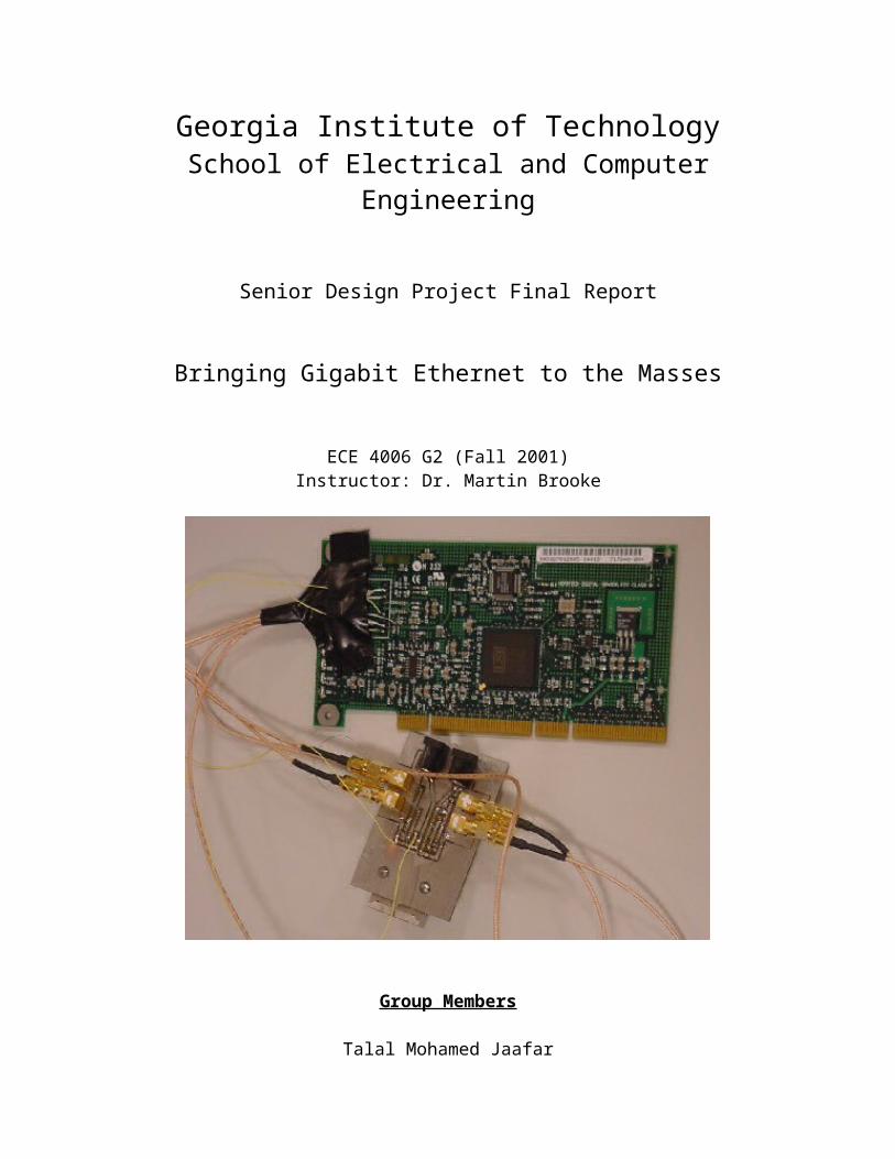
Georgia Institute of TechnologySchool of Electrical and Computer Engineering
Senior Design Project Final Report
Bringing Gigabit Ethernet to the Masses
ECE 4006 G2 (Fall 2001)Instructor: Dr. Martin Brooke
Group Members
Talal Mohamed JaafarIbrahima Bela Sow
Mohammad Faisal Zaman

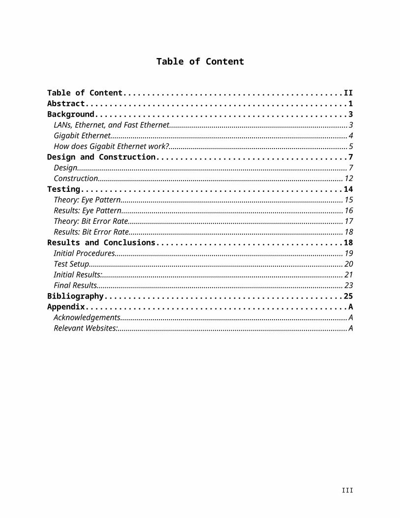
Table of Content
Table of Content...........................................................................................................................IIAbstract..........................................................................................................................................1Background....................................................................................................................................3
LANs, Ethernet, and Fast Ethernet..............................................................................................3Gigabit Ethernet...........................................................................................................................4How does Gigabit Ethernet work?...............................................................................................5
Design and Construction...............................................................................................................7Design...........................................................................................................................................7Construction...............................................................................................................................12
Testing...........................................................................................................................................14Theory: Eye Pattern...................................................................................................................15Results: Eye Pattern...................................................................................................................16Theory: Bit Error Rate...............................................................................................................17Results: Bit Error Rate...............................................................................................................18
Results and Conclusions..............................................................................................................18Initial Procedures.......................................................................................................................19Test Setup...................................................................................................................................20Initial Results:............................................................................................................................21Final Results...............................................................................................................................23
Bibliography.................................................................................................................................25Appendix........................................................................................................................................A
Acknowledgements.......................................................................................................................ARelevant Websites:.......................................................................................................................A
II
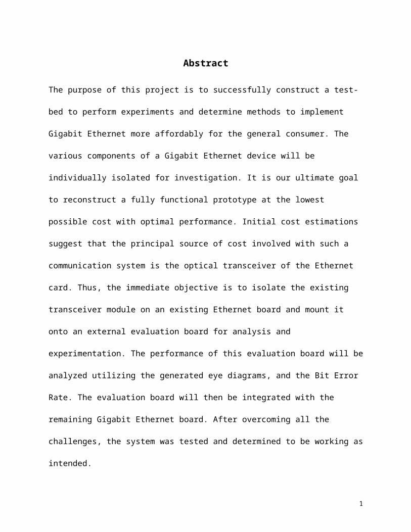
Abstract
The purpose of this project is to successfully construct a test-bed to perform experiments and
determine methods to implement Gigabit Ethernet more affordably for the general consumer.
The various components of a Gigabit Ethernet device will be individually isolated for
investigation. It is our ultimate goal to reconstruct a fully functional prototype at the lowest
possible cost with optimal performance. Initial cost estimations suggest that the principal source
of cost involved with such a communication system is the optical transceiver of the Ethernet
card. Thus, the immediate objective is to isolate the existing transceiver module on an existing
Ethernet board and mount it onto an external evaluation board for analysis and experimentation.
The performance of this evaluation board will be analyzed utilizing the generated eye diagrams,
and the Bit Error Rate. The evaluation board will then be integrated with the remaining Gigabit
Ethernet board. After overcoming all the challenges, the system was tested and determined to be
working as intended.
1
Introduction
At no other time in the history of human civilization has the importance of information
gathering, processing, and distribution been so critical. People are constantly checking their e-
mail, stock quotes, sports scores, banking online, etc. With the advancement of fiber optic
communication networks, people have been able to access information at speeds that were
unimaginable only a few years ago. However, as improvement to such existing networks
continues unperturbed, the number of beneficiaries from such technologies is not increasing at
the same rate. The fundamental problem is the cost involved in accessing these technologies.
Gigabit Ethernet technology is a prime example. Implemented as a major improvement over its
predecessors the Ethernet and Fast Ethernet; the Gigabit Ethernet (which has since been
experimentally succeeded by the 10-Gigabit Ethernet) is used by few to none in the general
public. The overall goal of this project is to achieve prices for Gigabit Ethernet that are
comparable to those of the usual 10BaseT Ethernet. In this leg of the project, the goal is the
construction of a test-bed to perform experiments and determine methods to implement Gigabit
Ethernet at a reduced cost. The various components of a Gigabit Ethernet device will be
individually isolated for investigation. Initial cost estimations suggest that the principal source of
cost involved in a fiber based Ethernet card is the optical transceiver. Thus, the immediate
objective is to isolate the existing transceiver module from an Intel Gigabit Ethernet board and
mount it onto an external evaluation board for analysis and experimentation. Once this task is
achieved, future groups that will work on this project can modify the transceiver and even
replace it by other systems safely, without running the risk of damaging the Ethernet card. In
addition, the new board that will be assembled can be used with other schemes of data
transmission to transmit video feeds for instance.
2
Background
LANs, Ethernet, and Fast Ethernet
Local area networks (LAN) were invented in the mid 1970s. The immediate future
development of LANs seems centered on enhancing what exists today by making the current
LANs faster, and more reliable rather than inventing something that is completely new. LAN
technologies operate at the Data Link layer (layer 2 of the OSI Reference Model), and Ethernet is
just one of many different LAN types.
Ethernet was invented in 1973 by Dr. Metcalfe, and it was conceived as a passive coaxial
cable medium (a physical and logical bus topology) with a contention-based medium access
protocol. The data transmission is done through broadcasting, and all the stations that are on the
network will be listening to the message. By contention-based medium we mean that only one
station may transmit at a time, so a protocol is needed to ensure that all stations will fairly share
access to the wire. Digital Equipments, Intel, and Xerox standardized the original protocol
envisioned by Metcalfe and it is known as “DIX” Ethernet.
In the early 1980s, the IEEE created a formal standardization framework to encompass all
existing and yet-to-be-invented LAN technologies. Ethernet is synonymous with the IEEE 802.3
for a 1-persistent CSMA/CD (Carrier Sense Multiple Access with Collision Detection) LAN.
CSMA/CD is the protocol that enables the medium (i.e. the wire) to be shared fairly among all
stations. “Carrier sense” means that every station that is about to transmit data has to sense the
cable to determine if it is being used by another station. If the cable is busy, then the station will
wait until the cable goes idle and then transmits its frame immediately. Another improvement in
the 802.3 protocol is that the stations will abort their transmissions as soon they detect a
collision. In other words, when two stations sense the cable to be free and start transmission at
the same time, they should stop transmitting their frames as soon as a collision is detected since
3
both frames will be garbled. The DIX Ethernet was used to connect more than 100 workstations
on a 1 km cable. Since the system was successful, it was standardized by as IEEE 802.3 with a
data rate of 10 Mbit/s. Initially there were two types of coaxial cables used. These were known
as Thick Ethernet (10Base5) and Thin Ethernet (10Base2). Later, the main type of cable used
was the unshielded twisted pair (UTP) copper cable.
As computer technology advanced, the demand for faster and more reliable methods of
communications has been increasing. The 10 Mbit/s DIX Ethernet did not provide enough
bandwidth to fulfill the users’ demands. That led to the standardization of the Fast Ethernet in
the form of IEEE 802.3u in 1995. The Fast Ethernet technology was defined for 100 Mbit/s,
which has ten times more bandwidth than the DIX Ethernet, and has improved features such as
full-duplex operation. The IEEE 802.3 networks used to operate only in half-duplex mode,
whereas the IEEE 802.3u networks allowed its stations to operate in full-duplex mode, which
enabled them to send and receive data simultaneously.
Gigabit Ethernet
Due to the unpredictable growth rate of the computer industry, there has been a major
demand for higher bandwidth communication channels. More than 120 companies united in the
Gigabit Ethernet Alliance to promote a new standard of Ethernet. The new IEEE 802.3z was
achieved in June 1998. The design objectives of the new standard were the following:
Offers high bandwidth of 1,000 Mbps.
Uses the IEEE 802.3 Ethernet frame format, with the addition of carrier extension field.
Employs the same half-duplex and full-duplex MAC operation schemes as the predecessors.
Addresses backward-compatibility with 10 Mbps and 100 Mbps Ethernet technologies.
Supports all existing network protocols.
4
The adopted physical layer of Gigabit Ethernet was Fiber Channel, a technology for
connecting workstations, supercomputers, storage systems, and peripheral devices. Also, the
Ethernet standard 802.3z (1000Base-X) supports transmission via multi-mode and single-mode
optical fibers as well as twinax cable. The transmission over twisted pair cabling was set up in
an independent standard known as IEEE 802.3ab (1000Base-T). The four physical media types
that the Gigabit Ethernet is based on are illustrated in Figure 1.
1 2 3 4
Figure 1. Gigabit Ethernet physical Layers.
How does Gigabit Ethernet work?
The Fiber Channel technology uses long wavelength lasers to transmit data over a fiber
optic cable. The IEEE 802.3z standard (also known as 1000Base-X) has defined three physical
layers: 1000Base-CX (short-haul copper), 1000Base-LX (long-wavelength optics), and
1000Base-SX (short-wavelength optics.) In addition, the IEEE 802.3ab created a physical layer
that allows the work over four pairs of cat5 UTP copper. 1000Base-SX uses short-wavelength
5
laser transmitters (770-860 nm) running over multi-mode fiber, and relatively short distances. In
contrast, 1000Base-LX uses long-wavelength laser transmitters (1270-1335 nm). 1000Base-LX
can run over multi-mode fiber and short distances, or over single-mode fiber and great distances.
The supported (coverage) distance is directly proportional to the type of fiber, as well as the
wavelength used, as shown in Table 1.
Table 1. Gigabit Ethernet over Fiber.
As shown above, the maximum traveling distance over a multi-mode fiber is 550m for
the 1000Base-SX, and 1000Base-LX. Also, the 1000Base-LX allows a traveling range up to
5000m over a single-mode fiber. At present short-wavelength are cheaper than long-wavelength,
and since 1000Base-SX goes nearly as far as the 1000Base-LX (500m comparing to 550m).
Hence it is more likely that most people would use the 1000Base-SX especially for LANs.
The copper-based physical layer in the 1000Base-X family is 1000Base-CX. 1000Base-
CX operates over two pairs of 150 shielded twisted pair cable. It was designed for sever-to-
switch interconnection in relatively small rooms. Thus, the distance was limited to 25m.
Another copper based physical layer is the 1000Base-T, which is being developed with a goal of
1000 Mbps operation over 100m category 5 unshielded twisted pair infrastructure. 1000Base-T
6
will use all four pairs of the RJ-45 connector and squeeze five times the bandwidth out of each
pair. As term of use, 1000Base-CX might be used for attaching servers to the Gigabit Ethernet
infrastructure over very short distances, and 1000Base-T will replace 1000Base-SX if it is
cheaper.
Design and Construction
DesignThe design portion of this project is the most important part because it will determine the
success of the project. Therefore, it is paramount that enough attention is given to the design of
the module that is being put together. As stated in the previous portion of this report, the goal of
the project is to detach the fiber-optic transceiver from the Ethernet board and mount it on a
separate circuit board that is outside the computer, and that will be the new experimental board
that can be used to test and modify the optics of the Ethernet card. The first step involved in the
design is the identification of the parts of the Ethernet board that have to be moved with the
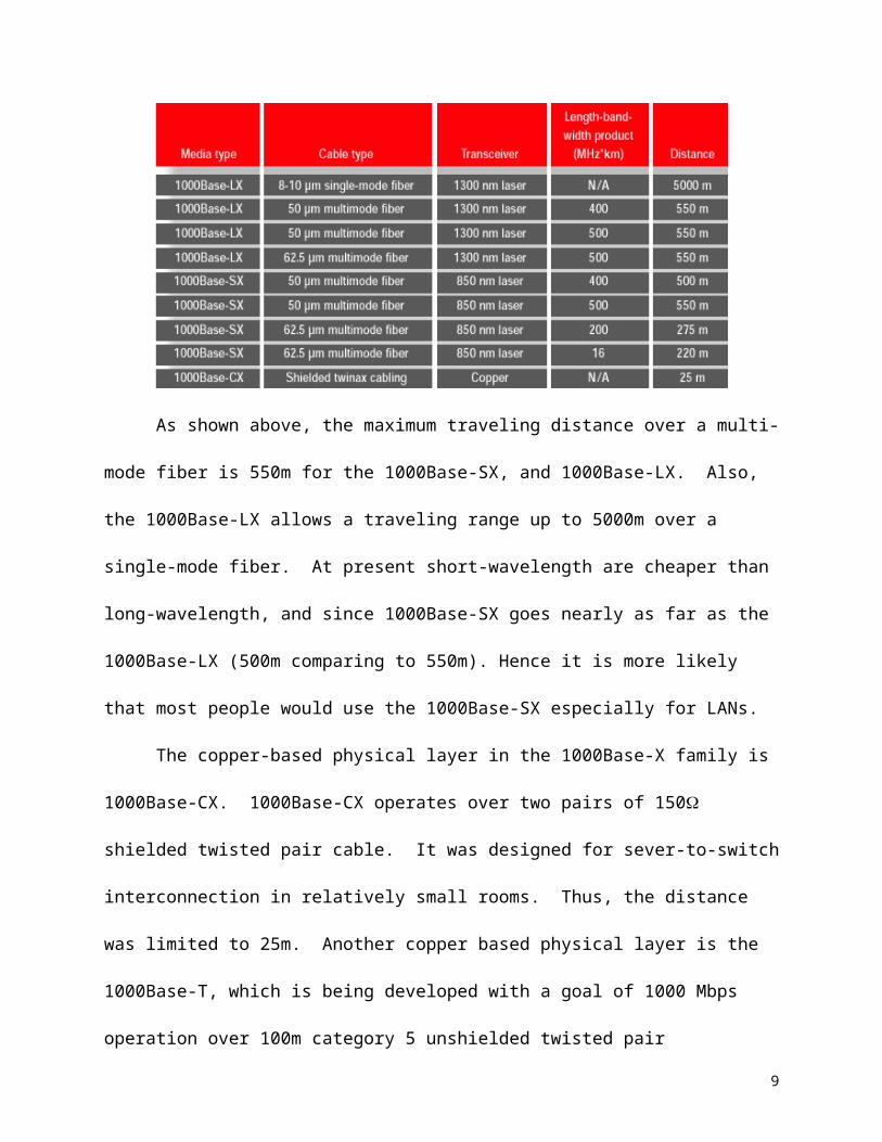
HFBR- 53D5 fiber-optic transceiver to form the new opto-electronic module. The circuit
diagram in figure 2 shows the complete circuitry of the Intel Ethernet card.
7
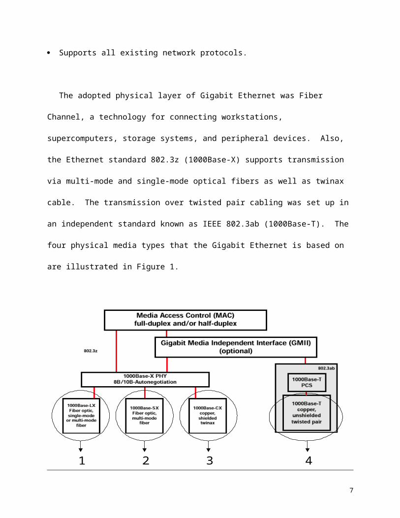
Figure 2. Intel Pro/1000 Gigabit Ethernet circuit diagram
The task at hand involved the following challenges. Proper coupling of the power lines,
proper decoupling of the ac lines, proper grounding of the external board and properly soldering
all the surface mount components, which is a serious challenge due to the size of the
components.
Once the components that will be moved to the experimental board were identified, they
were erased from the circuit diagram and the diagram in figure 3 was obtained. Essentially, the
experimental module will contain the HFBR-53D5 Fiber-Optic Transceiver, power supply
connectors, signal transmission SMA jacks and the circuitry associated with the transmission
lines and the power supply.
8
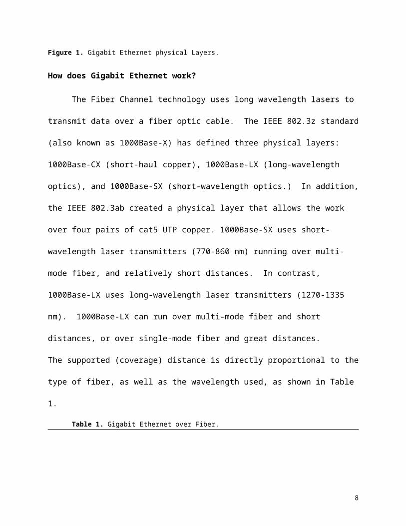
Figure 3. Circuit that will be designed for the experimental board.
On the Intel Pro/1000 Ethernet Card, the transceiver was powered by a special power
supply system that was essentially a single power supply that used a filtering circuit to keep the
Transmitter’s power supply separate from the Receiver’s power supply, in order to prevent the
two supplies from interfering with each other and noise from propagating from one side to the
other through the power lines. Since the addition of the filtering circuitry would increase the
complexity of the experimental board, it was decided to simply use two 5V DC power supplies,
which can be found at Radio Shack. The only drawback to this approach is the addition of the
power supply jacks to the experimental board and the fact that every time the board is used, two
power supplies have to be plugged to the wall outlet. The connection between the experimental
module and the board will be done through coaxial cables. The challenge here is the selection of
coaxial cables that can support the speeds involved. Essentially, the system is sending digital
signals at one Gbits/s using unipolar NRZ (non return to zero) signaling. This translates to a
square wave that can be estimated to have a fundamental frequency of 500MHz, and to get a
proper signal it is advisable to pass the first 5 harmonics; therefore, the coaxial cables that are to
be used should handle at least 2.5GHz. For this reason, RG-316 coaxial cables were chosen.
9
These cables can handle speeds up to 3 GHz or more, and they offer another advantage, which is
that they are small so they will not be too cumbersome. On the Ethernet Card, the coaxial cables
will be directly soldered to the holes where the pins of the transceiver were located, and on the
experimental board, the coaxial cables will be attached using SMA connectors so that the board
can be detached from the Ethernet Card at any time. The choice of the SMA connectors was
mainly due to the size of the cables, the speeds involved, and the amount of space available on
the experimental board. SMA connectors can handle speeds up to 18 GHz, while regular BNC
connectors at best will handle only 3 GHz. Providing ample space on the experimental board is
very important because later groups will have to work on the board and probably modify some
parts of it; therefore, considering the size of the surface mount components, it is paramount that
they have enough space to be able to work comfortably on the board.
Among the components of the circuit shown in figure 3 are the transmission line
termination resistors, DC de-coupling capacitors and AC coupling capacitors. The transmission
line terminations are required because the board is big enough for the traces on it to be
considered transmission line. Therefore, impedance matching is absolutely necessary to avoid
harmful reflections in the lines. The role of the AC coupling capacitors is to keep harmful DC
components that might slip into the signals from ever reaching the transceiver on the Tx side, or
the Ethernet card on the Rx side. DC signals in the high-speed AC lines have the potential to
cause some signal distortions and attenuation, and thus detection problems. Essentially AC
coupling consists of simply passing the signals through a high pass filter formed by a capacitor
and usually the impedance matching resistor of the line. These can be clearly seen in the circuit
diagram of figure 4. The DC de-coupling capacitors have to counter act the inductance
introduced by the power supply lines and the grounds. A conductor has the undesirable behavior
of acting like an inductance as its length increases, the effect of this behavior, as frequencies
10
increase is that the impedance of the line also increases drastically. To deal with this problem,
DC de-coupling capacitors are used to counteract the inductance of the lines. The DC de-
coupling capacitors also protect the circuit from the transient current pikes that results from the
very fast switching and they also help reduce the noise levels on the power supply lines.
The other notable feature of the design is the maintenance of the differential signaling
scheme used on the original Ethernet card. Differential signaling has some benefits that cannot
be ignored in such a design. In essence, using differential signaling is like using two copies of
the signal in the detection phase. One wire is the positive leg of the path and the other is the
negative leg. There are two big differences. First, the two wires carry inverted copies of the
voltage waveforms, meaning when one wire has a rising edge on it, the second has a falling edge.
The second is that the receiver compares the two signals, producing a 1 whenever the signal on
the positive leg is greater (more positive) than that on the negative leg. It produces a 0 when the
opposite is true. Another way of saying this (which justifies the word ‘differential’) is that the
two Voltage signals are subtracted (positive – negative) and a positive result is a 1 and a negative
result is a 0. Differential signals have much better noise immunity. This can be seen by thinking
mathematically about what is happening. Let’s assume the positive leg has a value of P and the
negative l leg has a value of N. Then the sign of the subtracted signals P – N is the result of the
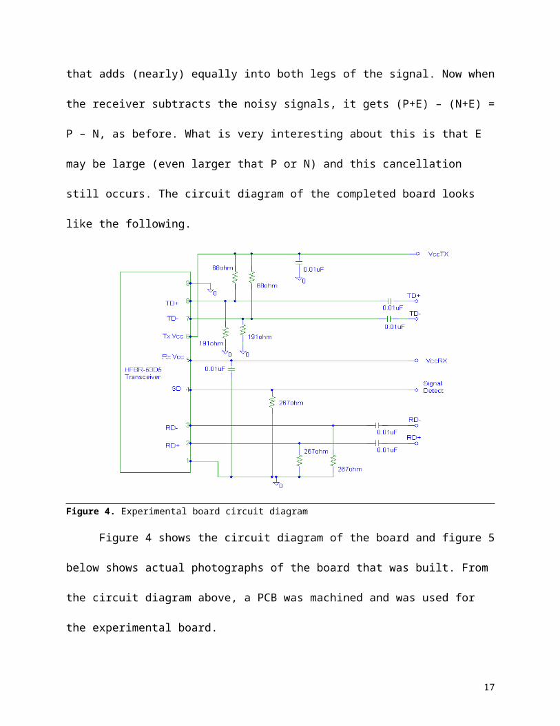
signal. Now let’s add a noise error E. This gives us P+E and N+E, because most noise sources
cause common mode noise, or noise that adds (nearly) equally into both legs of the signal. Now
when the receiver subtracts the noisy signals, it gets (P+E) – (N+E) = P – N, as before. What is
very interesting about this is that E may be large (even larger that P or N) and this cancellation
still occurs. The circuit diagram of the completed board looks like the following.
11
Figure 4. Experimental board circuit diagram
Figure 4 shows the circuit diagram of the board and figure 5 below shows actual
photographs of the board that was built. From the circuit diagram above, a PCB was machined
and was used for the experimental board.
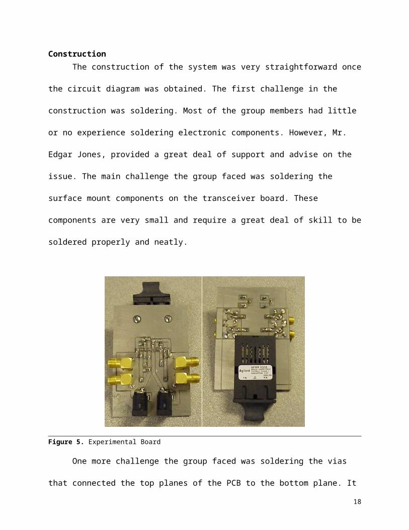
ConstructionThe construction of the system was very straightforward once the circuit diagram was
obtained. The first challenge in the construction was soldering. Most of the group members had
little or no experience soldering electronic components. However, Mr. Edgar Jones, provided a
great deal of support and advise on the issue. The main challenge the group faced was soldering
the surface mount components on the transceiver board. These components are very small and
require a great deal of skill to be soldered properly and neatly.
12
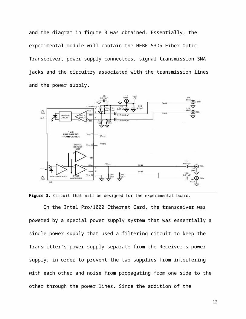
Figure 5. Experimental Board
One more challenge the group faced was soldering the vias that connected the top planes
of the PCB to the bottom plane. It is very easy to overlook soldering the pieces of wire that go
through the vias, and it is necessary to caution future groups that will be using these boards
against overlooking the vias and most importantly soldering over them while soldering the other
components. Finally, the last issue in the construction was connecting the ground planes of the
power supplies to the pins of the power supply jacks. The ground pins are located directly
beneath the jacks and were inaccessible once the jacks were seated on the board. This problem
was overcome by simply dripping solder on the opposite side to the jacks (solder side) and
letting it drip along the pin onto the plane that is beneath the jack. It is important to note here that
the signal detect (SD) lines were established between the experimental board and the Ethernet
card using a simple wire that was thin enough. And the ground on the experimental board will be
connected to the ground on the Ethernet card, to provide a common reference voltage, using the
same type of wire as the SD line.
13
Testing
The experimental board was tested to determine its performance with random data. Of
particular interest were the eye diagram and the bit error rate. Figure 6 shows the general
experimental setup used while testing the performance of the experimental board. The setup
comprises the following components:
Figure 6. Test Setup for Gigabit Ethernet
1. Programmable binary signal generator: Used to generate random bit patterns with
specified frequency to be used to do a performance analysis on the receiver.
2. High-Speed sampling oscilloscope: Utilized to observe the eye pattern.
3. Experimental board: The experimental board with mounted opto-module transceiver and
completed circuitry is tested. The experimental board contains the power supply and the
SMA jacks.
4. Fiber-optic cable: Two separate lengths (10 ft. and 50 ft.) of cable were utilized. Bit Error
Rates at either length were recorded to account for attenuation concerns.
14
5. Power Supply: Two 5 Volts Power supplies were utilized to power the experimental
board.
The eye pattern test was setup by attaching the receiver’s SMA connectors to Channel 1
and Channel 2 of the Oscilloscope, while the two SMA connectors of the transmitter were
attached to the binary signal generator. Disconnecting the receiver from the oscilloscope and
attaching it to a BERT allows for Bit Error Rate testing.
Theory: Eye Pattern
While implementing any baseband pulse-transmission communication system the effects
noise and intersymbol interference raises great concerns. A very useful experimental tool for
performance analysis is the eye pattern, which is defined as the synchronized superposition of all
possible realizations of the signal of interest (e.g. received signal, receiver output) viewed within
a particular signaling interval. The eye pattern derives its name from the fact that it resembles the
human eye for binary waves. The interior region of the eye pattern is called the eye opening.
An eye pattern provides a great deal of useful information about the performance of data
transmission and receiver systems. A sample diagram with the characteristic features is shown in
Figure 7. Three points that can be highlighted are the following:
15
Figure 7. Interpretation of the eye pattern
1. The width of the eye opening defines the time interval over which the received signal can
be sampled without errors due intersymbol interference. So it is practical to sample at the
time instant when the eye is open the widest.
2. The sensitivity of the system to timing errors is determined by the rate of closure of the
eye as the sampling time is varied.
3. The height of the eye opening, at a specified sampling time, defines the noise margin of
the system.
Results: Eye Pattern
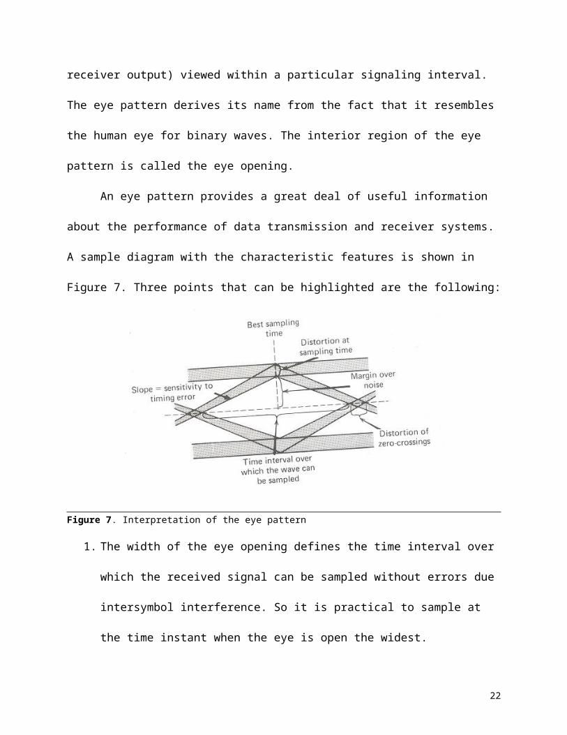
Figure 8. Eye Pattern Observed with PN-7 encoding (with 10ft Cable)
The initial test was run with a data input stream of 1.4 Gbps using a PN-7 encoding
scheme. The eye pattern observed on the scope is depicted in figure 8. Preliminary analysis
indicates a sufficiently good eye opening to justify optimal performance from the experimental
board setup. Noise rather than ISI seems to be the dominant problem. This is apparent by the
16

slope that indicates sensitivity to timing errors and comparing it to the noise margin. Another
clear observation is the fact that channel 1 and channel 2 outputs are opposite of each other,
which was expected since the experimental board uses differential signals.
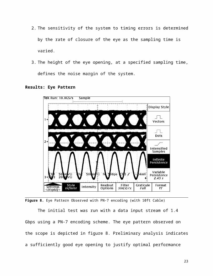
Figure 9. Eye Pattern Observed with PN-7 (with 50ft Cable)
To determine the effects of attenuation on the experimental board performance a different
length of optical fiber cable was utilized. In our case the 10-ft. cable was replaced with a 50-ft
wire. No noticeable degradation of the eye pattern was noticed, as shown by figure 9, which is
almost identical to figure 8, suggesting that the effects of attenuation can be neglected. The
second part of the experiment is to determine the Bit Error Rate. At this point the receiver
terminals were connected to the BERT.
Theory: Bit Error Rate
In telecommunication transmission, the bit error rate (BER) is the percentage of bits that
have errors relative to the total number of bits received in a transmission, usually expressed as
ten to a negative power. For example, a transmission might have a BER of 10 to the negative 6
17
(10-6), meaning that, out of 1,000,000 bits transmitted, one bit was in error. The BER is an
indication of the likelihood that a packet or other data unit being retransmitted because of errors.
Too high a BER may indicate that a slower data rate would actually improve overall
transmission time for a given amount of transmitted data since the BER might be reduced,
lowering the number of packets that had to be resent. A BERT (bit error rate test or tester) is a
procedure or device that measures the BER for a given transmission.
Results: Bit Error Rate
BER testing was conducted using two encoding schemes, the PN-7 and a more
complicated PN-23 encoding scheme. Tests were run with several data streams with rates beyond
1.0 Gbps rate. The results are shown in table 2.
Table 2. BER Testing Results (with cable length 50-ft)
PN-7 (Encoding Scheme) PN-23 (Encoding Scheme)1.0 Gbps Negligible Negligible1.2 Gbps Negligible 2.2 x 10^-61.4 Gbps Not Tested Too High
The PN-7 scheme, in which at most seven 1’s or 0’s are sent consecutively, shows a
sufficiently acceptable BER at speeds of 1.0 and 1.2 Gbps. However the test results the PN-23
scheme (which is a more complex and rigorous scheme because it sends up to twenty-three 1’s or
0’s in a row) produced a significant error at 1.2 Gbps. Finally, the performance of the
experimental board was poor at 1.4 Gbps data rate.
Results and Conclusions
The final step of the project was the integration of the experimental board with the Intel
Gigabit Ethernet board and testing the performance of the setup. Two separate computers were
required to perform the test. One computer contained a standard Intel Gigabit Ethernet card. The
other computer contained the Intel Gigabit Ethernet card that was interfaced with the
18
experimental board. Initially the Intel Gigabit Ethernet Diagnostic software was used to test
transmission performance of test packets between the two computers. After this was completed
successfully, practical data files (e.g. JPEG, .DOC) were transferred between the two computers
to verify that they were networked properly. Thus, validating the results of the project.
Initial Procedures
In order to successfully integrate the experimental board with the Gigabit Ethernet card, it
was required to remove the redundant components present on the Gigabit Ethernet board. These
components, primarily the impedance matching resistors, were already present in the
experimental board. Presence of these extra components would result in redundant components
that would cause malfunctions.
Figure 10. Experimental board Integrated with Gigabit Ethernet Card
The boxes in figure 10 show the redundant components on the Ethernet board. These
components were removed carefully using a pair of pliers. The figure also shows the coax
connections from the Experimental board to the Gigabit Ethernet Board. In addition, Pin 1 on the
Experimental board was connected to pin 1 on the Ethernet board to provide a common ground,
19
and pin 4 on the Experimental board was connected to Pin 4 of the Gigabit Ethernet Board to
connect the signal line. The removed components on the actual board and the completed
experimental system are shown in figure 11. The red markers show the location of the resistors
that were removed and the yellow markers indicate pins 1 and 4.
Figure 11. Experimental board interfaced with the modified Gigabit Ethernet card.
Test SetupFigure 12 shows in detail the setup for analyzing the performance of the Gigabit Ethernet
Card integrated with the experimental board.
20
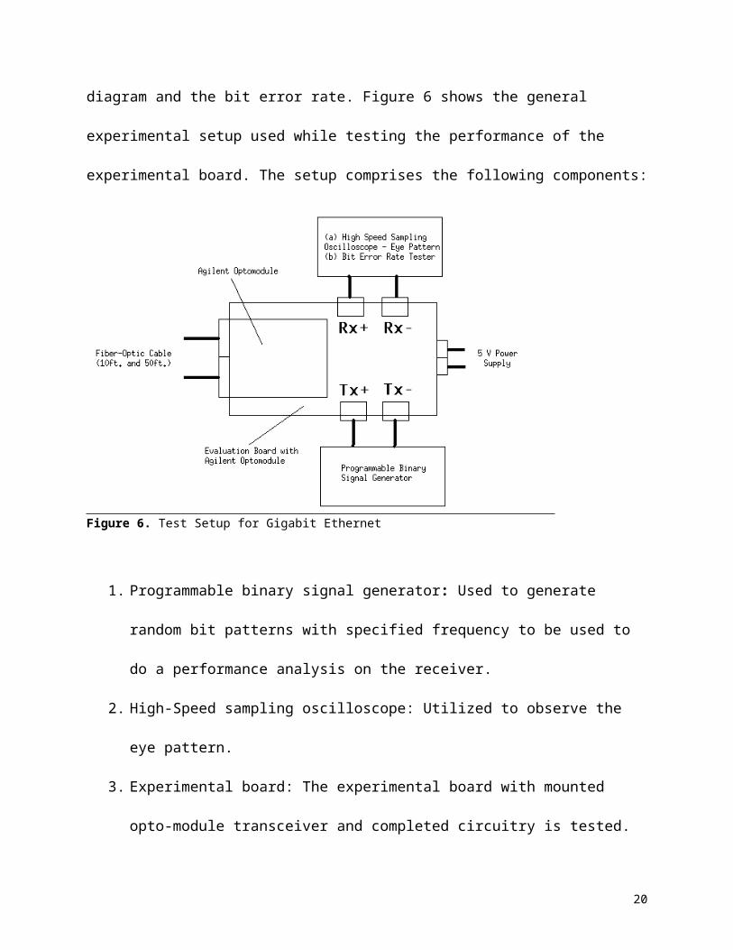
Figure 12. Experimental setup for testing the designed Gigabit Ethernet card.
1) Experimental board, which is attached to the Experimental Ethernet card.
2) RG-316 Co-axial Cables, which connect the transmitter and receiver ‘s SMA connectors to their respective pins on Gigabit Ethernet Card.
3) Experimental Gigabit Ethernet Card
4) 50ft. Roll of Optical Fiber.
5) 5 Volts power supplies powering the receiver and the transmitter.
6) Oscilloscope used to verify the presence of the Signal Detect signal.
7) The two computer screens used to test the transfer of data between the two computers.
Initial Results:Having the Experimental system directly looping back to itself and using the Diagnostic
software (Intel(R) PROSet), the designed board passed all the basic diagnostic tests: Control
Registers, FIFO Registers, EEPROM, Interrupt, Loopback, and Link.
21
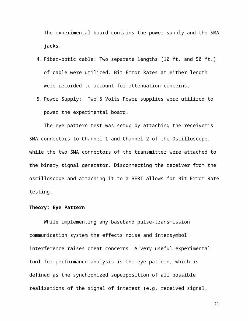
Figure 13. Diagnostic test preliminary results.
Next, the diagnostic software was used to send test packets between the experimental Gigabit
Ethernet system (as Sender), and the unmodified Gigabit card (as Responder) residing in another
computer. The Experimental Gigabit system was able to send packets, but failed to receive the
responses. The test was done using short and long fiber cables, and the results were the same.
All the connections were checked multiple times, and the experimental board was scrutinized to
make sure there were no loose connections.
Figure 14. Initial connections. Figure 15. Enhanced connections.
22
A few preliminary tests were conducted to identify the source of the problem, to see
whether there was a problem with the Gigabit Ethernet Board or the Experimental Board or both.
First, the experimental board was interfaced with a different Gigabit Ethernet card, and the test
results were successful. Hence, the problem was determined to be in the interfaced Gigabit
Ethernet card, and the problem was assumed to be related to a bad trace from Pin 3 that was
existent on the board. However, careful examination suggested otherwise.
Upon the advice of Dr. Brooke our attention was focused on the distance between the
connections and the meshes of the signals. Theoretically, a transmission line must be uniform on
the scale of the wavelength of signals traveling along it, and a discontinuity in the line will
reflect the signal, but if the discontinuity is very small the signal will not be disrupted. The
discontinuity must be less than 10% of the wavelength of the signal to avoid any signal
interactions and harmful reflections. In the test process, using a 500MHz square wave, the data
signal could be seen as the third harmonic (at 1.5 GHz.) The wavelength of the signal can be
calculated using the following equation:
(Where is the relative dielectric constant ~ 3)
This equation yields a wavelength of approximately 10 cm, so the minimum discontinuity
distance should be no more than 1cm (10% of the wavelength.) As illustrated in figure 14, the
mesh of the coaxial cable of the connection indicated by marker 2 was all the way back at
position indicated by marker 1; in addition, the distance is obviously more than 1 cm. To fix this
problem, the connection was rewired and the new layout is illustrated in figure 15.
Final Results
After successfully tackling the connection problem the same experimental procedures
were repeated. This time the test setup worked perfectly. The computers were able to transmit
23
and receive test packets between them. Both computers were used as sender and responder, and
data packets were transmitted and received on either end. The resulting screenshots are shown in
figure 16.
Figure 16. Diagnostic test results for “test packets” transmission between the two cards.
Upon successfully sending test packets between the two computers, the final part of the
project was to test the transmission of useful data files between the two computers. This was
achieved by sending one image file and one MS word file. The files were transferred and opened
successfully.
Lastly, the system is tested and proven to work. It is the hopes of this group that the
experimental boards constructed will be used effectively to better the state of data communication
systems.
24
Bibliography1. Tanenbaum, Andrew S., Computer Networks. New Jersey: Prentice Hall. 1996
2. “Gigabit_Ehternet”, August 9, 1999. http://www.syskonnect.com/syskonnect/technology/Gigabit_Ethernet.PDF
3. “Gigabit Ethernet”, December 2, 2000. http://www.comm.toronto.edu/~karen/projects/21.GbEthernet-802.3/overview.html
4. “Ethernet Web”, January 31, 2000. http://www.ots.utexas.edu/ethernet
25
Appendix
AcknowledgementsThe group member would like to thank
Dr Martin Brooke: For all the support, guidance, and the great advice. This would have never happened without him.Edgar Jones: For all the help with equipment and soldering issues.Harsh Sopory: For letting us use their board for troubleshooting.The members of all the other groups for helping make this a fun experience.
Relevant Websites:www.digikey.com They have most of the parts that were used in this project.www.agilent.com The makers of the opto transceiverwww.intel.com The makers of the Gigabit Ethernet board.
A
![0)#1'(#23#& .'%15'6%)#$'7#81*95, - Duke Universitypeople.ee.duke.edu/~sjt/assets/RFID2011_SmartHAT_pres.pdf · Orbit Communications Pty Ltd. [Online]. Available: [2] W. H. Schiffbauer](https://img.pdfslide.us/doc/110x75/5aee92717f8b9a903191462c/0123-15678195-duke-sjtassetsrfid2011smarthatprespdforbit.jpg)