Embed Size (px)
Citation preview
Abstract
Gigabit Ethernet technology is the next stage for high-speed networking. In
addition to electronics, it utilizes fiber optic technology and is built upon the existing
Ethernet architecture. This paper focuses on the timeline of the engineering process
involved in building a 1.25 Gbps Optoelectronic link. The project involves designing,
building and testing the transmitter and receiver circuits necessary for the data link. The
receiver board was designed, built, tested, and worked optimally. The transmitter board
design did not function as desired and compelled the group to reconsider scheduled
activities and focus on determining the problem. Ultimately, the problem was identified
and fixed resulting in a working transmitter and optoelectronic link. The group’s progress
was hindered by faulty equipment and not investing enough time in a second design. The
group learned from the fundamental errors in the first transmitter and receiver
fabrications to propose their second design. They are convinced that given more time to
obtain and build their second fabrication, it would work on the first try.
1
Introduction
Of all the current networking protocols, Ethernet has the highest number of
installed ports, and provides the greatest cost performance relative to Token Ring, Fiber
Distributed Data Interface (FDDI), and ATM for desktop connectivity. Ethernet has
evolved greatly since its inception at Xerox Corporation in the early 1970s. The advent
of Fast Ethernet enabled networking speed to increase from 10 to 100 megabits per
second (Mbps). This enabled Fast Ethernet to provide a simple, cost-effective option for
backbone and server connectivity.
In June 1998, a new protocol was standardized for the new dominant player in
high-speed local area network backbones and server connectivities. This protocol was the
Gigabit Ethernet technology. Gigabit Ethernet enables an increase in speed of tenfold
over Fast Ethernet to 1000Mbps or 1 gigabit per second (Gbps). Since it is built on top of
the Ethernet protocol, it would enable customers to utilize their existing knowledge base
to manage and to maintain such a new technology. For more information, go to:
http://www.cisco.com/warp/public/cc/techno/media/lan/gig/tech/gigbt_tc.htm.
To allow for the speed increase from 100 Mbps Fast Ethernet up to 1 Gbps,
changes needed to be made to the Gigabit Ethernet architecture. The Gigabit Ethernet
architecture essentially looks identical to that of Ethernet from the data link layer
upwards, but the changes reflect inclusions from the ANSI X3T11 FiberChannel
technology. The IEEE 802.3Z standard architecture for the Gigabit Ethernet is
summarized in Figure 1.
http://www.ece.gatech.edu/academic/courses/ece4006/fall2002/group3/figure1.doc
This paper will focus on building part of the Physical Media Dependent (PMD)
Layer of the Gigabit Ethernet architecture. For this project, a transmitter and receiver will
be designed and built for a 1.25 Gbps Optoelectronic link. The design of the
Optoelectronic data link is illustrated in Figure 2.
http://www.ece.gatech.edu/academic/courses/ece4006/fall2002/group3/figure2.doc
The serial and differential data input from the transmitter drive the laser driver to
produce a modulated light signal from the Vertical Cavity Surface Emitting Laser
(VCSEL) that is transmitted down the fiber optic cable. The modulating light signal is
2
detected by the photodetector in the receiver, and the signal is amplified to give an
output.
The laser driver, transimpedance and limiting amplifiers that will be used in the
transmitter and receiver design are the MAX3287, MAX3266 and MAX3264 chips
provided by the semiconductor company MAXIM Integrated Products.
The MAX3287 is a high-speed laser driver for fiber optic LAN transmitters that is
optimized for Gigabit Ethernet applications. The chip is equipped with an automatic
power control that adjusts the laser’s bias current to maintain an average optical power.
The MAX3287 chip can be configured with a short wave 850nm VSCEL for Gigabit
Ethernet use. The typical features of the chip include 3.0V to 5.5V supply voltage, 30mA
laser modulation current and temperature compensation for modulation current (3). The
complete information about the MAX3287 can be found on the MAXIM data sheet
currently at http://pdfserv.maxim-ic.com/arpdf/MAX3286-MAX3299.pdf.
The MAX3266 is a transimpedance amplifier (TIA) for 1.25Gbps fiber optic
receivers. The TIA amplifies small PD (photodiode) current with low noise and has low
input impedance, about 600 Ohms. Another function of the TIA is to convert current to
voltage. The chip features 3.0V to 5.5V single supply voltage, 200nA input-referred
noise, and 929MHz bandwidth (4). For complete data information about the MAX3266
TIA refer to the MAXIM quick view data sheet currently at http://pdfserv.maxim-
ic.com/arpdf/MAX3266-MAX3267.pdf
The 1.25Gbps MAX3264 limiting amplifier chip is designed for Gigabit Ethernet
optical receiver systems, which accepts a wide range of input voltages and provides
constant level-output voltages. The limiting amplifier boosts the TIA output voltage. The
limiting amplifier features a 3.0 to 5.5V supply voltage, low deterministic jitter, a choice
of CML or PECL output interface (5). For complete data information about the limiting
amplifier, refer to the MAXIM data sheet currently at
http://pdfserv.maxim-ic.com/arpdf/MAX3264-MAX3765.pdf.
PhotodetectorsPhoto detectors are used to detect the incoming light signal from the transmitter.
Photodetectors are usually of the P-I-N form where a p-type and n-type semiconductor
has an intrinsic region in between. Photodetectors have three characteristics that are
3
critical in optoelectronic data links. These are the photodetector responsivity, capacitance
and receiver area. Maximizing the receiver area allows more coupling between the fiber
optic line and the photodetector. Responsivity is a term used to describe the sensitivity of
the photo detector, which is given in Amps of current per Watt detected (A/W). Smaller
capacitance values decrease the response time for the photo detector, which is critically
important for the high speed that data is being transmitted.
VCSELsThe Vertical-Cavity Surface-Emitting Laser (VCSEL) is used as the optical
source of Gigabit Ethernet and many other data communication systems. The foremost
application of VCSELs is to transmit optical signals for coupling into optical fibers.
VCSELs are generally fabricated by employing proton-ion implantation, by dry etching,
or a selective oxidation for current isolation. There are four important characteristics of a
VCSEL that need to be considered when selecting appropriate types of VCSELs for this
design. These characteristics are the threshold current, the slope efficiency, the emitted
power, and aperture size of the VCSEL. The lasing threshold current is determined by the
difference between the gain and loss at the lasing wavelength. It is the minimum current
that is needed to drive the VCSEL into lasing. The slope efficiency is the incremental
increase in power for an incremental increase in current usually given with units of mill
watt per milliamp (mW/mA). Once again, the fiber optic cable should be properly
aligned to allow for maximum coupling.
For this project, unconnectorized as well as connectorized photodetectors and
VCSELs are considered. This is because the connectorized components have already
been adjusted for maximum coupling and would be used to verify a working transmitter
and receiver board. The unconnectorized components shall be used after the transmitter
and receiver board designs are verified later, to investigate the effect of optical fiber
coupling.
Division of LaborThe first action taken by the group was to divide the required tasks among the
group members according to their specialties and competence. Each person was assigned
one or two specific tasks that they would be responsible for. Through group meetings
each person would present their findings and give recommendations. This sharing of
4
Table 1. Labor Division.
Position PersonLeader Jason Herrington
Vendor Specialist Jason Herrington
Measurement Specialist Man Le
PD Specialist Shahriar Khushrushahi
Solder Specialist Nickolas Kingsley
Webmaster Nickolas Kingsley
Head Editor Robiel Teclemichael
Head Writer Shahriar Khushrushahi
VCSEL Specialist Man Le
Electromagnetics Specialist Nickolas Kingsley
knowledge amongst the individuals in the group would enable any group member to
temporarily assume another member’s role if that person was not able to complete a task
because of other obligations. The specific areas assigned can be seen in Table 1 and are
described in detail below.
The group leader was responsible for assigning tasks for completion before the
next group meeting or presentation, and to make sure that all points assigned to be
covered in the group meetings were discussed. In addition, the group leader was
responsible for tracking group progress on the Gantt chart to assure that the current group
progress matched or exceeded the projected values. Jason Herrington was appointed as
group leader through group consent.
The responsibility of the vendor specialist was to contact, place orders and
follow-up the delivery of group orders with vendors. This position is extremely time
critical because of the limited project time and the possible of long lead-time of some of
the components to be ordered. An unexpected challenge of this position was found to be
in working around the schedules of the people holding the purchasing credit cards. Jason
Herrington volunteered and was group appointed for this position because of extensive
vendor relations experience from past co-op responsibilities.
5
The Measurement Specialist’s responsibilities primarily involve familiarity with
the test equipment in the lab to expedite group component and circuit testing. The person
appointed for this position was Man Le.
The next two positions that needed to be filled were photo diode and VCSEL
specialists. These two team members were responsible for all research involving photo
detectors and VCSELs respectively. These included the responsibilities for the initial
selection of connectorized and unconnectorized photodetectors and VCSELs for use in
the groups’ circuits, the writing of background and component selection sections in the
report papers, and the presentation of all pertinent data in the group meetings. Man Le
was chosen as VCSEL specialist and Shahriar Khushrushahi was chosen as PD specialist.
The responsibility of the Solder Specialist was to solder the 0805 packaged
passive components and the 8 and 16 pin CUE and CSA packaged integrated circuits to
the provided and group designed fabricated circuit boards. This position required a high
level of soldering skill to conduct soldering quickly and efficiently to reduce the chance
of an integrated circuit or passive component being damaged from over-heating.
Nickolas Kingsley had a large amount of past soldering experience and performed
adroitly at this task.
Nickolas Kingsley also volunteered to be the web master for the group as well.
The responsibility of the web master includes the creation and upkeep of the group
website. Nicolas Kingsley exceeded the expectations of the group by providing a group
logo which can be seen in Figure 3, and by creating a secure section of the website
several weeks before the idea of a group secure area was discussed in class. The website
can be visited currently at
http://www.ece.gatech.edu/academic/courses/ece4006/fall2002/group3
The final two positions were head writer and head editor for the group reports.
The responsibility of the head writer was to collect individually written sections of the
reports from each group member and compose these into a flowing presentation of the
group progress. The responsibility of the head editor was to check the paper for
grammatical or word usage errors. Shahriar Khushrushahi volunteered to be the head
writer and Robiel Teclemichael volunteered to be the head editor.
6
Chronological Design Progress Reports Week 1: August 25- 29 th 2002
On the first group meeting, research was conducted on the Maxim chips data
sheets for upcoming design considerations. In addition, the IEEE 802.3Z standard in its
entirety was located and the appropriate data was extracted. This data gave an idea of the
specifications involved for the design, primarily in determining the criteria necessary for
the selection of the appropriate photo detectors and VCSELs. The necessary data
extracted is tabulated as follows in Figure 3.
http://www.ece.gatech.edu/academic/courses/ece4006/fall2002/group3/standard.doc
Strategies were drawn up early on to allow for risk mitigation. These included
Early high productivity to give time for “unpredicted” circumstances later in
the semester
Have multiple vendors for each product in case of backorder or shipping
problems
Rigorous checking and rechecking all designs and solder jobs.
Plan to order multiples of each component to account for any defective or
damaged components
Week 2: August 30th-September 5 th 2002
The team, on the first attempt, assembled the provided board and generated an
open eye. The eye diagram for the 50 dB attenuated K28.5 data pattern is illustrated in
Figure 4.
http://www.ece.gatech.edu/academic/courses/ece4006/fall2002/group3/figure4.doc
Figure 5 illustrates an eye diagram for a 50 dB attenuated PRBS7 data pattern
with little jitter suggesting a near perfect implementation of the receiver board.
http://www.ece.gatech.edu/academic/courses/ece4006/fall2002/group3/figure5.doc
The remaining eye diagrams from 50 dB down to 10 dB all looked exactly the same as
Figure 5. For attenuations above 60dB, the output was complete noise.
A preliminary list of candidate photodetectors was comprised. They were drawn
up using the criteria from the IEEE 802.3Z standard such as operating wavelength of
770-860nm and signal speed of 1.25Gbps. The companies included Anadigics, Advanced
Photonix, Honeywell, Luxnet Corporation, Photonic Detectors and Lasermate.
7
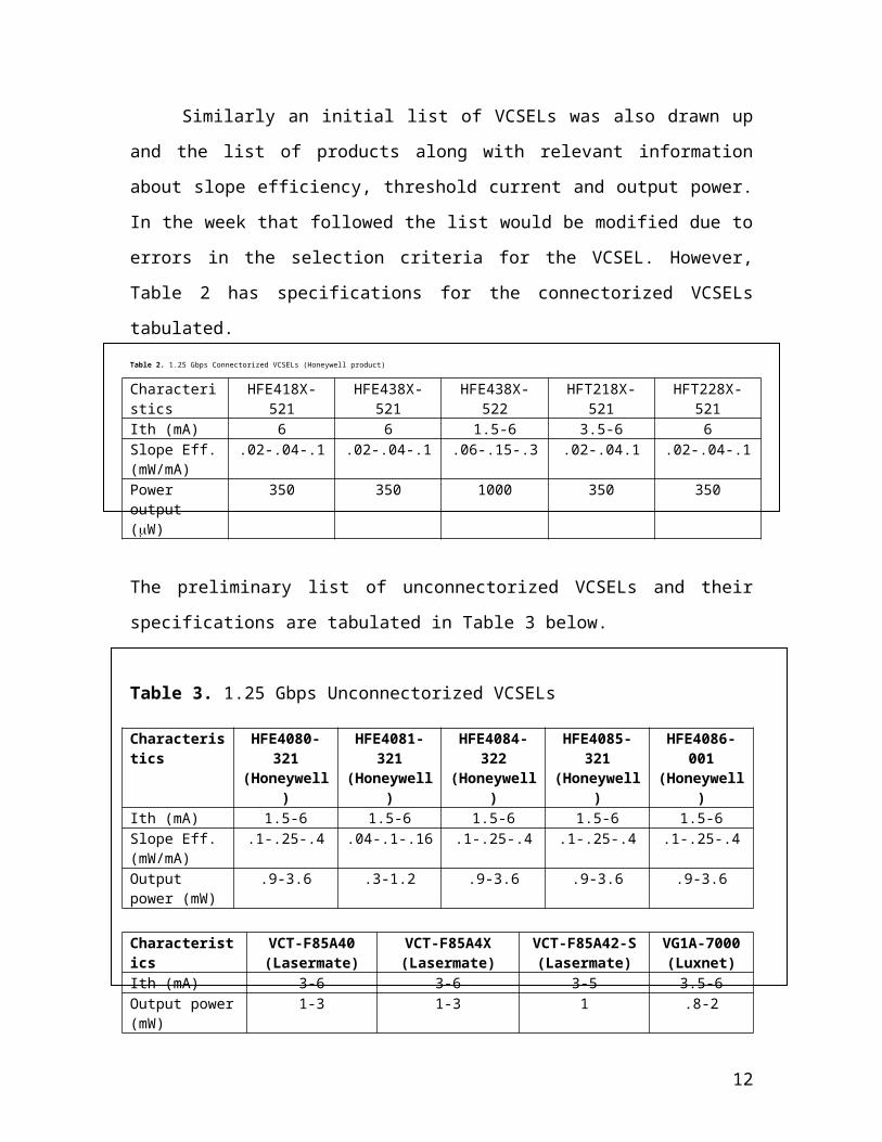
Similarly an initial list of VCSELs was also drawn up and the list of products
along with relevant information about slope efficiency, threshold current and output
power. In the week that followed the list would be modified due to errors in the selection
criteria for the VCSEL. However, Table 2 has specifications for the connectorized
VCSELs tabulated.
Table 2. 1.25 Gbps Connectorized VCSELs (Honeywell product)
Characteristics HFE418X-521 HFE438X-521 HFE438X-522 HFT218X-521 HFT228X-521Ith (mA) 6 6 1.5-6 3.5-6 6Slope Eff. (mW/mA)
.02-.04-.1 .02-.04-.1 .06-.15-.3 .02-.04.1 .02-.04-.1
Power output (W)
350 350 1000 350 350
The preliminary list of unconnectorized VCSELs and their specifications are tabulated in
Table 3 below.
Table 3. 1.25 Gbps Unconnectorized VCSELs
Characteristics HFE4080-321(Honeywell)
HFE4081-321(Honeywell)
HFE4084-322(Honeywell)
HFE4085-321(Honeywell)
HFE4086-001(Honeywell)
Ith (mA) 1.5-6 1.5-6 1.5-6 1.5-6 1.5-6Slope Eff. (mW/mA)
.1-.25-.4 .04-.1-.16 .1-.25-.4 .1-.25-.4 .1-.25-.4
Output power (mW)
.9-3.6 .3-1.2 .9-3.6 .9-3.6 .9-3.6
Characteristics VCT-F85A40(Lasermate)
VCT-F85A4X(Lasermate)
VCT-F85A42-S(Lasermate)
VG1A-7000(Luxnet)
Ith (mA) 3-6 3-6 3-5 3.5-6Output power (mW)
1-3 1-3 1 .8-2
Slope Eff. (mW/mA)
.25 .25 .25-.3 .15-.3-.5
Power Budget
The purpose of calculating the power budget is to trace the flow of power though the
system. This will allow the engineer to choose components that are compatible. A trace
of the system was shown previously in Figure 2. The following are key issues in the
power budget calculation:
Not overdriving the VCSEL
8
Driving the VCSEL such that the average output power is 1 mW
Calculating the passive component values
The following values were given from either the VCSEL spec, the PD spec, or the IEEE
802.3z standard (shown in Figure 3, previously):
VCSEL Threshold current (Ith)
VCSEL Slope Efficiency (η)
VCSEL Beam Divergence (Defined by )
PD responsivity (R)
PD Dark Current
PD Capacitance
Fiber loss
The following values are vitally important in ensuring a working board and must be
calculated:
VCSEL DC bias current (Ibias)
VCSEL Modulation current (Imod)
VCSEL Total current (Itot)
VCSEL Output Power (Pout)
Modulation resistance (Rmod)
Bias resistance (Rbias)
Power loss due to the fiber
To meet eye safety standards, the output of the VCSEL should be, on average, as close to
1mW as possible. The formula for calculating Pout is:
(Eqn. 1)
Pout, typical can be assumed to equal 1 mW and the maximum can be assumed to equal 2
mW (even though the value is greater than the eye safety limit, it will be 1 mW on
average). Since Pout, η, and Ith are known, Itot can be calculated.
Two formulas for the VCSEL DC bias current are given in the MAXIM 3287
spec (3, page 14):
(Eqn. 2)
9

(Eqn. 3)
Combining Equations 2 and 3 results in:
(Eqn. 4)
Since Itot has been calculated and Ith is given, Imod can be calculated. Equations 2 or
3 can be used to calculate Ibias.
Calculating the potentiometer values (Rmod and Rbias) seemed to be very straight-
forward in the first draft of the power budget. The value of Rbias was originally
determined from a formula given on page 14 of the MAXIM 3287 spec (3, page 14):
(Eqn. 5)
The value of Rmod was determined from the Electrical Characteristics section on page
three of the MAXIM 3287 spec. There are three Imod values and their respective Rmod
values. Using linear interpolation, an approximate formula was derived to model their
relationship. This formula is shown in Equation 6.
(Eqn. 6)
Equations 5 & 6 result in Rbias and Rmod values between 500-700 ohm.
The loss of power due to the fiber can be calculated from information given in the
IEEE 802.3z standard (Figure 3). The maximum loss due to fiber is 7.5 dB. This
calculates to 0.1778 watts coming out of the fiber for each milliwatt sent in. Naturally,
this is the worst-case scenario and the actual loss should be much less. The maximum
attenuation is approximately 3.75 dB/km. For a one-meter fiber, the loss is only 0.391%.
For a one hundred meter fiber, the loss is 0.860%. In addition, there is at most 2.38 dB
connectorization loss. The IEEE standard also notes that the receive sensitivity is
approximately -17 dBm. This calculates to a sensitivity of approximately 19.95 μW!
Clearly, this is very sensitive equipment.
The group web page with group logo was launched and everyone in the group
placed an order for samples of the MAXIM chips to be used. This would help in the
construction of the transmitter and receiver boards.
The Gantt chart from the second week is shown in Figure 6
http://www.ece.gatech.edu/academic/courses/ece4006/fall2002/group3/figure6.doc. It
illustrates all the individual tasks to be accomplished as well as the timeline involved.
10
The light blue color was used to signify possible tasks pertaining to that week, whilst the
dark blue color was used to signify definite projected tasks.
Week 3: September 5-September 12 th 2002
The individual groups in the class were given information pertaining to the
financial budget allocated for the project. Each group is allocated a budget of $350.00 for
the purchasing of all the necessary components for the implementation of the design of
the optoelectronic link. A rough financial budget was determined for this group given the
information that it would cost $62 per PCB fabrication and that two fabrications were to
be done. This would leave around $100 for photodetectors and VSCELs each, and the
remaining budget would be utilized for passives and other unforeseen expenses.
A budget of $100 for the photodetectors and VCSELs mean that the type of PDs
and VCSELs to be purchased has to be correct. However, there were problems
encountered from the first list of photodetectors and VCSELs drawn up that had to be
dealt with. These were as follows:
Several of the photodetectors drawn up had different types of packaging such as
TO-46 and TO-18. The question that had to be answered was whether the
packaging type influenced the photodetector functionality. What was determined
was that the packaging that the various photodetectors used would not make a
difference but an additional criterion that surfaced was the receiver area.
Several of the photodetectors had units of responsivities as mV/W, which
differed from the expected units of A/W. The significance of this difference was
that such photodetectors turned out to have a pre-amplifier built in. This would
mean that there was no need for the MAXIM TIA 3264 chip, since the PDs
behave as a preamplifier. Hence, if the photodetectors with the pre-amplifiers
were to be utilized, the receiver design would have to be modified to remove the
MAXIM 3264 chip.
Some of the VCSELs chosen had built-in photodiodes, pre-amps and different
kinds of lenses (ball lens, flat lens etc). These additional components would affect
the entire design and would be more expensive than the standard VCSEL
11
The solutions to the problems that were encountered helped in adding additional
criteria not only to narrow the list of photodetectors and VCSELs in mind, but also to
acquire greater understanding of the project and its requirements. The team opted to keep
the MAXIM 3264 chip and leave the receiver design untouched.
In addition, further criteria were added that helped in narrowing down the list of
photodetectors and VCSELs. Such additional criteria are:
The need for both connectorized and unconnectorized photodetectors and
VCSELs. The connectorized photodetector and VCSEL would be used to ensure
that our designs work since they have been adjusted for optimum alignment. The
connectorized photodetector and VCSEL would have an SC receptacle. Whereas
the unconnectorized components would require tweaking the design to minimize
alignment losses.
The need for a range of responsivities for the connectorized and unconnectorized
photodetectors, as well as a range of slope efficiencies for the connectorized and
unconnectorized VCSELs to test the robustness of our design
The need for a small capacitance to allow for fast response times and also to allow
for proper functionality of the MAXIM chips involved in the circuit.
These new criteria suggested that the search for photodetectors and VCSELs had to be
started all over again. But all the work done up till then was not in vain, this time an idea
of what to look for and what not to look for had been established. The Gantt chart for the
third week is shown in Figure 7.
http://www.ece.gatech.edu/academic/courses/ece4006/fall2002/group3/figure7.doc
The Gantt chart was not very clear with respect to its color-coding, and it was
suggested in the class presentation to have an improved Gantt chart. This was because it
did not illustrate what tasks were accomplished and what task was late.
Week 4: September 12-September 26 th 2002
A final list of VCSELs and photodetectors that would be used for the design of
the boards was made and the items were ordered. The lists of ordered components and
their specifications are tabulated in Appendix A.
The photodetectors were chosen with a range of responsivities in mind, having
low end responsivities of 0.3 A/W to high end responsivities of 0.55A/W. There are also
12

three capacitance values that needed to be investigated, 0.45pF, 1.2pF and 1.5pF. These
apply to the unconnectoriezed photodetectors. Despite rigorous searching only one
connectorized photodetector was found, the LASERMATE RSC M85A306. This
variation in specifications will help test the robustness of the receiver design.
The VCSELs were also chosen with a range of slope efficiencies, threshold
currents and power outputs in mind. The range of slope efficiencies would determine the
amount of power that the receiver would be able to detect, hence would determine the
robustness of the design. For instance, the HFE4381-512 has low-end slope efficiency,
which is about 0.04 mW/mA. This is a relatively inexpensive VCSEL and if it were to
work with the design it would help reduce the total cost of the design. The other VCSELs
chosen, example the HFE4384-522, has a very wide range of slope efficiencies, 0.06-0.3
mW/mA that matches the worst and the best-case scenarios. Finally, the best and most
expensive VCSEL is chosen with a slope efficiency of 0.1-0.4 mW/mA. This VCSEL has
the highest probability of working within the design and would be used for the worst-case
scenario to guarantee that the design works. The power outputs were chosen keeping in
mind that the average output power should be within the eye safety limit of 1 mW.
The schematics for the receiver and transmitter board were completed along with
the actual receiver PCB layout. The circuit for the design of the transmitter board is
shown in Figure 8.
http://www.ece.gatech.edu/academic/courses/ece4006/fall2002/group3/figure8.doc
While working on the layout of the transmitter and receiver boards, there were
three guidelines that were followed:
1. Avoid transmission lines by keeping signal lines as short as possible. Lines less
than 7mm are acceptable, but less than 4mm would be best.
2. Lines that must be long should be angled at 45 degrees
3. Ground plane should be present whenever possible to minimize fluxing magnetic
fields
With only a few exceptions, all signal lines were kept below 4mm in length. The
second draft of the transmitter PCB board went for review. The layouts and their
revisions are illustrated in Appendix B.
13

The PCB layout had enough space for an additional design to be squeezed in. This
enabled the team to add a slighly different design of the transmitter on the PCB layout.
The new design of the transmitter added to the board was to investigate the effect of a
different VCSEL orientation in the design. The Gantt chart for week four is illustrated in
Figure 9.
http://www.ece.gatech.edu/academic/courses/ece4006/fall2002/group3/figure9.doc
The revised Gantt chart for this week was a considerable improvement from its
predecessors. It clearly illustrates the time elapsed from the crosshatch markings. The
brown blocks indicate tasks accomplished while the green blocks indicate what is
planned. The Gantt charts for all the following presentations follow the same format and
are illustrated in Appendix C.
Week 5: September 26-October 3 rd 2002
Several VCSELs and photodetectors were received. However, there were several
issues encountered in the course of ordering and receiving the parts for our circuits.
These included receiving a different VCSEL than the one ordered from Lasermate. This
was because the part number ordered was out of stock and the substitute VCSEL would
perform comparably the same to the one ordered.
There was additional delay for the delivery of the packages. United Parcel Service
(UPS), the shipper chosen as default for all orders, sent the packages to Georgia Institute
of Technology Central Receiving, which added one to two days to the delivery time of all
packages.
The only positive issue encountered was in contacting Allied Electronics in
Norcross, Georgia. Through Lindy, a customer service agent, the team was able to get
samples for several Honeywell connectorized and unconnectorized VCSEL’s.
In addition the passive components had to be ordered, these included ferrite
beads, capacitors, potentiometers, and resistors.
Ferrite Beads
The ferrite beads used in the transmitter board act as inductors to reduce
deterministic jitter. The MAXIM 3286 (LAN Laser Driver- page 16) specification sheet
recommends using the Murata BLM11HA102SG ferrite bead. These particular
components have a DC resistance less than 1.6Ω and impedance greater than 100Ω at the
14

design operating frequency. The ferrite beads were bought from Mouser Electronics at
$0.25 each. The dimensions are illustrated in Figure 10.
http://www.ece.gatech.edu/academic/courses/ece4006/fall2002/group3/figure10.doc
Potentiometers
Each transmitter circuit uses two potentiometers to adjust the current that drives
the VCSEL to 1 mW output power (to meet eye safety specifications). The Panasonic
6mm Square Carbon Trimmer Potentiometers were chosen because of their small size,
reliable manufacturer and availability. Since the exact value of the pots is unknown,
several pots of various values; 500, 1K, 10K, and 20K ohm, were ordered from Digi-Key
at a price of $0.41 each. Figure 11 illustrates the dimensions of the potentiometers.
http://www.ece.gatech.edu/academic/courses/ece4006/fall2002/group3/figure11.doc
The overall budget, including the passives ordered, is illustrated in Table 1 of
Appendix D. Also, the final version of the transmitter and receiver layout were approved
by Professor Brooke and the printer circuit boards (PCBs) were ordered from Express
PCB. The final PCB layouts for the transmitter and receiver boards are illustrated in
Figure 12.
http://www.ece.gatech.edu/academic/courses/ece4006/fall2002/group3/figure12.doc
The two transmitter designs are on the left while the receiver design is on the far
right.
Week 6: October 3rd-October 10th 2002
The ExpressPCB boards arrived on time. Figure 13 is a picture of one of the
fabrication layouts that was obtained.
http://www.ece.gatech.edu/academic/courses/ece4006/fall2002/group3/figure13.doc
Notice that all signal lines are less than 7mm in length and all lines are angled
when possible.
The components were soldered and the receiver board was tested using the
connectorized photodetector. The receiver board did not work on the first attempt and
after considerable “debugging,” two problems were identified.
1. Ground pin from power connector was not connected to the backplane
2. Pin 14 of the limiting amplifier was not soldered correctly.
15

It was decided that a second construction of the receiver would help in eliminating solder
problems or faulty chips in the first failure of the receiver board.
Soldering
Although Nickolas Kingsley serves as the group’s soldering specialist, everyone
in the group has contributing to the soldering effort. Fortunately, during the first half of
the semester there were no major soldering issues. Despite Dr.Brooke’s recommendation,
flux was never used to solder. In addition, the soldering iron was rarely set above 650oF,
which is relatively cool compared to what the iron is capable of. During this week, most
of the receiver and transmitter components were receieved.
Week 7: October 15th-October 17th 2002
The second construction of the receiver board was accomplished and tested
through a short patch cable and the 100 meter spool of fibre. The eye obtained was
perfect. Figure 14 illustrates the K28.5 eye diagram using the fiber optic cable.
http://www.ece.gatech.edu/academic/courses/ece4006/fall2002/group3/figure14.doc
Figure 15 illustrates the eye obtained when testing the receiver board with PRBS7
data pattern and the fiber optic cable.
http://www.ece.gatech.edu/academic/courses/ece4006/fall2002/group3/figure15.doc
Appendix F illustrates the remaining eye diagrams when utilizing the patch cable for both
PRBS7 and K28.5 data patterns.
Week 8: October 17th-October 24th 2002
During this week the group concentrated on finishing the first report and the
transmitter debug process. Scheduled for this week was the alignment tolerance of the
receiver board. However since the group had not finished the previous task of building a
working transmitter design, the group was behind its proposed schedule. A reorganization
of responsibilities took place to help pull the group back on track.
Transmitter Debug
The group was divided into two subgroups. The first subgroup consisting of
Jason Herrington and Nickolas Kingsley were responsible for the continued debug of the
transmitter. The remaining members of the group were tasked to measure the alignment
tolerance of the receiver board.
16
It was determined during transmitter testing that the power rating of the
potentiometers utilized was too low (0.1Watts). It was hypothesized that potentiometers
with a power rating of 0.3 watts would be better.
Alignment Tolerance Testing
Alignment tolerance testing was one of the most important processes in
determining the robustness of the board design. To evaluate the robustness of the board
design, cheaper components and components with lower parameter values are utilized to
see if the board still functions optimally. The group decided to utilize the Hamamatsu
S7911 first instead of the Lasermate PDT-A85A30, since it had a higher responsivity and
less capacitance giving it a higher chance of success.
The set up for the receiver alignment tolerance testing is as shown in Figure 16.
http://www.ece.gatech.edu/academic/courses/ece4006/fall2002/group3/figure16.doc An
oscilloscope was used to display the output data while the signal generator generates the
signals that were fed to the receiver board. One 62.5/125m cleaved multi-mode fiber
was connected from the receiver of the generator signal module to the window of the
photodiode. The two outputs of the receiver board were connected to the appropriate
channels of the oscilloscope. The core of the fiber had to be perfectly aligned with the
window of the photodiode to absorb the most signals.
The fiber was set so that it had the best open eye out of the receiver, and this
position was used as the reference position. The fiber was moved in the xy, xz and yz
plane. Each measurement was done in increments of 10 micrometers until the output
had a bad eye. At each move, the magnitude of the output signal was measured. This
process was performed for the xy, yz, and xz planes. Those data was recorded and then
plotted as shown in Figure 17.
http://www.ece.gatech.edu/academic/courses/ece4006/fall2002/group3/figure17.doc
The graphs give the ratio of power received with respect to the reference position as a
function of the x, y and z directions.
Week 9&10: October 24th-November 6th 2002
By November 6th group 3 should have had the transmitter and receiver boards
working. They should have also made changes and submitted the new PCB transmitter
17
and receiver layouts. However, the group had some problems getting the transmitter
design to work. It was determined that instead of going ahead with submitting another
PCB layout, it was decided that the group determine the exact reason for the failure of the
transmitter board and make sure that the transmitter design works.
Transmitter Debug
The transmitter subgroup found three additional problems with the transmitter
board. One problem was that the ground of the power input was not connected to the
back plain of the board. This was corrected by soldering a wire between the ground of
the power input and the back plane of the board. These correctional changes were also
made to the PCB layout immediately to avoid the possibility of forgetting to do so if
group 3 were to have another board fabrication. The second problem had to do with one
terminal of the potentiometers connected to VCC. The other problem had to do with not
choosing correct values for the potentiometers dealing with the bias and modulation
current. These problems are highlighted in Figure 18.
http://www.ece.gatech.edu/academic/courses/ece4006/fall2002/group3/figure18.doc
The group had to decide whether there was something inherently wrong with
either the transmitter design or the power budget. The transmitter design was determined
to be accurately done leaving the power budget open for revision.
In dealing with the transmitter design debugging, an additional concern was
brought up. The group had in their possession only two connectorized VCSELs
remaining. Considering that it would take a month at most to order new components, it
would have been a considerable risk to go on testing the transmitter hoping that the
power budget was sufficient. Instead the group had in their possession several
unconnectorized VCSEL components. It was proposed that an unconnectorized VCSEL
be used instead to see if there was any sign of life in the circuit.
This debugging is shown in Figure 19.
http://www.ece.gatech.edu/academic/courses/ece4006/fall2002/group3/figure19.doc
The test with the unconnectorized VCSEL gave no good results, further emphasizing
problems with the power budget.
18
Alignment Tolerance Testing
In class, the exact method for alignment tolerance testing was laid out. After
having the best eye at the reference position, the fiber was moved in the positive x
direction until 10 dots were observed inside the clear optimum eye on the oscilloscope as
in Figure 20 (the oscilloscope was set to 10 second persistence).
http://www.ece.gatech.edu/academic/courses/ece4006/fall2002/group3/figure20.doc.
This process was repeated for positive and negative x and y direction. The method was
applied for the S7911 PD and the results were obtained as in Figure 21
http://www.ece.gatech.edu/academic/courses/ece4006/fall2002/group3/figure21.doc.
The large circle in Figure 21 was the active working area of the S7911 where the
fiber at reference position, and the small circle was the working area where the fiber is
0.87 millimeters above the reference position.
Week 11: November 7th-November 14th 2002It was confirmed that the initial power budget drawn up was rudimentary and
considerable work had to be done to determine the correct values for the bias and
modulating current potentiometers. The power budget went under revision and was
continually being verified with Dr. Jokerst and Dr. Brooke. The group managed to
purchase two connectorized VCSELs from Dr. Jokerst & Brooke to aid with the
transmitter debug process.
Transmitter DebugThe transmitter subgroup built another transmitter layout since it was suspected
that the incorrect potentiometer values used in the previous designs might have damaged
the MAXIM chips. By building a new design with new parts, any additional errors that
would hinder the debugging process would be eliminated. The connectorized VCSEL
was lowered as close to the board as possible (to minimize transmission line effects). In
addition, the leads of the VCSEL were clipped as close to the board as possible to avoid
possible RF effects that would cause signal degradation.
Alignment Tolerance TestingThe receiver sub-group were ready to continue alignment tolerance testing
utilizing the other photodiode, Lasermate PDT-A85A30. However, the signal generator
module had burnt out that week leaving all the groups handicapped.
Week 12: November 15th-November 21th 2002
19
Transmitter Debug
The final errors in the power budget were eliminated. Calculating the
potentiometer value for Rbias proved to be problematic in the first draft of the power
budget. The value of Rbias was originally determined from a formula given in Equation 5:
(Eqn. 5)
However, this approximation made some assumptions about the circuit that are not
applicable to this project. This formula resulted in Rbias values between 50-100 ohm.
Resistance values this small fried the pots and the VCSEL each time the circuit was
powered up. The final formula for calculating Rbias is shown in Equation 7.
(Eqn. 7)
Equations 5 & 7 result in Rbias values between 500-700 ohm and Rmod values between
11.5k-15k ohm. The updated power budget is available here.
http://www.ece.gatech.edu/academic/courses/ece4006/fall2002/group3/
powerbudgetfinal.xls. The correct values of the potentiometer were determined and
soldered onto the transmitter board. The first power up of the board gave an eye from the
connectorized VCSEL ending the transmitter debug process and confirming that our new
optical budget calculations were flawless.
Alignment Tolerance Testing
The new signal generator module enabled the receiver subgroup to test the
receiver with the relatively inferior PD, the Lasermate PDT-A85A30. The PDT-A85A30
component had a small cap lens giving it the effect of a convex lens. This meant that the
photodiode could not detect signal when the fiber was too close to the photodiode
window. After setting the reference position for the photodiode, the fiber was moved 0.2
mm below this position and 0.72 mm above to perform testing at these two positions to
find out the characteristics of this photodiode. The middle circle in Figure 22
http://www.ece.gatech.edu/academic/courses/ece4006/fall2002/group3/figure22.doc was
the active working area of the photodiode at the reference position; the inside and outside
circles were the active working areas of photodiode at the 0.2 mm below and 0.72 mm
above relative to the reference position.
20
Some differences were observed from the results of two photodiodes shown in
Figure 21 and Figure 22. The active working area of the S7911 was about two times of
the active working area of the PDT-A85A30. This suggested that the S7911 performs
much better than the PDT-A85A30. This confirmed what was hypothesized from the
data sheets of the two photodiodes. The S7911 had capacitance = 0.45 F, responsivity =
0.47 A/W, and aperture = 0.1 mm while the PDT-A85A30 had capacitance = 1.2 F,
responsivity = 0.3 A/W, and aperture = 0.06 mm. The photodiode with lower
capacitance value responded much better. However, a greater aperture gave rise to a
greater active working area of the photodiode. The cost of the S7911 photodiode was
$21.31 while the PDT-A85A30 was only $28. This justified that the S7911 would be
ideal to purchase since it gave an improved performance for a relatively lower cost.
Week 13: November 22th-November 29th 2002The group began VCSEL alignment tolerance testing the HFE4081-321. VCSEL
alignment tolerance testing was much more difficult than PD testing. One reason being
that there was no guarantee that the vendor tested the individual components. Another
reason was if the vendor did test the part, there was no guarantee that the testing done
was adequate enough.
As a result, group 3 attempted the alignment tolerance testing by starting with the
fiber as close to the VCSEL window as possible and slowly moving the fiber in the X-Y
plane. Unfortunately, there were numerous problems with this process. Firstly, the optical
receiver on the signal source was not strong enough to receive enough signal power from
our transmitter. To fix this problem, we purchased a connectorized photodiode and used
it in our receiver circuit. The group’s connectorized photodiode receiver board was used
instead of the function generator receiver since it had greater sensitivity and could detect
any signal from the VCSEL with our unconnectorized VCSEL. Group 3 was able to get
some signal out of the VCSEL as a result.
Another problem faced was the lack of working fibers. Other groups would break
fibers and leave them unmarked for the next group. To guarantee that a fiber was
working, tests would have to be done with the working receiver board. If it worked with
the receiver, it was assumed it would work with our transmitter. Two different VCSELs
(HFE4081-321 & HFE4084-322) and countless optical fibers were tried, but even the
21
best signal gave mostly noise. Doubt whether the transmitter had another flaw was
resolved by retesting the transmitter with a connectorized VCSEL.
Due to the lack of time, more unconnectorized VCSELs could not be ordered and
the members of the group were confident that given more time, a working
unconnectorized VCSEL system could have been assembled.
Each group member contributed to part of the final paper which was due the
following week.
Financial Budget
For the design of the low price but efficient optoelectronic data-link, each group is
allocated a budget of $350.00 for the purchase of all the necessary components for the
implementation of the design. After accessing the power budget of the design and
deciding which components will be used for the design, the components were purchased.
The financial assessment for group 3 is summarized in Table 4.
Table 4. Financial Budget of Group 3
Purpose Amount Paid Balance
Beginning Balance
Budget allowed to each group
- $350.00
Total Purchases $331.79 $18.21
Remaining Balance - $18.21
As Table 4indicates, the group was able to implement the design of the optoelectronic
link with a total amount of $331.79. The detailed financial assessment of group 3 can be
found in Appendix D
22
ConclusionGroup 3’s members were very committed right from the beginning of the
semester. They were keen on striving to be ahead of the schedule to allow for unforeseen
complications. This determination led the team to get ahead of themselves and overlook
important considerations that were brought up when the transmitter board was being
tested.
However, the team’s careful risk mitigation strategies, reorganization, and
engineering mindset for solving problems helped in pin pointing and fixing the problem.
This is in spite of the limited number of parts that were available to test and debug the
design, as well as the damaged equipment in the laboratory.
The group was able to accomplish the receiver alignment tolerance testing
successfully; however, the group did not have the time to complete the alignment
tolerance testing of the transmitter board. This was primarily because of the lack of
working fibers available to them during the group’s working hours. In addition, the lack
of time also restricted the group from comparing the two possible designs of the
transmitter board to determine the better design.
The inferior power budget that was initially proposed formed the crux of the delay
in the proposed schedule. If the group had invested more time in the start in the power
budget, the group would have easily adhered to the schedule. This would have helped
determine the better of the two transmitter designs, VCSEL alignment tolerance testing
and build and test of the second fabrication. Nevertheless, a lot was learnt in the process
and the group managed to fix the power budget and design a new layout that would be
built if there was enough time.
If there was enough time to order and test a second board fab, these are changes
that would have been made:
1. Connected Rmod to ground instead of power2. Added a series resistor to the modulation pot for measuring Imod
3. Increased the size of the vias to make re-soldering easier
These changes are shown in Figure 23. http://www.ece.gatech.edu/academic/courses/ece4006/fall2002/group3/figure23.doc
23
Overall, the group is confident that they have no more fundamental flaws in the
understanding of the project. The group enjoyed the entire design process since it enabled
the group to employ commendable strategies and problem solving techniques in critical
times where resources were minimal and problems difficult to determine.
24
Works Cited1. “ IEEE 802.3Z Standard ”
2. “ Maxim Quick View Data Sheet “ available at
http://pdfserv.maxim-ic.com/arpdf/MAX3286-MAX3299.pdf
3. “ Maxim Quick View Data Sheet “ available at
http://pdfserv.maxim-ic.com/arpdf/MAX3266-MAX3267.pdf
4. “ Maxim Quick View Data Sheet “ available at
http://pdfserv.maxim-ic.com/arpdf/MAX3264-MAX3765.pdf
25


![0)#1'(#23#& .'%15'6%)#$'7#81*95, - Duke Universitypeople.ee.duke.edu/~sjt/assets/RFID2011_SmartHAT_pres.pdf · Orbit Communications Pty Ltd. [Online]. Available: [2] W. H. Schiffbauer](https://img.pdfslide.us/doc/110x75/5aee92717f8b9a903191462c/0123-15678195-duke-sjtassetsrfid2011smarthatprespdforbit.jpg)