Embed Size (px)
Citation preview
Introducing Carbon Diffusion Barriers for Uniform, High-QualityGraphene Growth from Solid SourcesRobert S. Weatherup,1 Carsten Baehtz,2 Bruno Dlubak,1 Bernhard C. Bayer,1 Piran R. Kidambi,1
Raoul Blume,3 Robert Schloegl,4 and Stephan Hofmann1,*1Department of Engineering, University of Cambridge, Cambridge CB3 0FA, United Kingdom2Institute of Ion Beam Physics and Materials Research, Helmholtz-Zentrum Dresden-Rossendorf, 01314 Dresden, Germany3Helmholtz-Zentrum Berlin fur Materialien und Energie, D-12489 Berlin, Germany4Fritz Haber Institute, D-14195 Berlin-Dahlem, Germany
*S Supporting Information
ABSTRACT: Carbon diffusion barriers are introduced as ageneral and simple method to prevent premature carbondissolution and thereby to significantly improve grapheneformation from the catalytic transformation of solid carbonsources. A thin Al2O3 barrier inserted into an amorphous-C/Nibilayer stack is demonstrated to enable growth of uniformmonolayer graphene at 600 °C with domain sizes exceeding 50μm, and an average Raman D/G ratio of <0.07. A detailedgrowth rationale is established via in situ measurements,relevant to solid-state growth of a wide range of layeredmaterials, as well as layer-by-layer control in these systems.
KEYWORDS: Graphene, solid carbon, low temperature, diffusion barrier, in situ, XPS, XRD
The application potential of graphene depends entirely onthe development of growth and integration techniques
that are scalable and allow an adequate level of structuralcontrol and material quality.1 While chemical vapor deposition(CVD) is widely seen as the most promising approach for this,a potentially equally versatile but much simpler, cheaper andless hazardous technique is the catalytic graphitization of solidcarbon sources. Carbon is thereby not supplied from the gasphase as in CVD, but rather as solid carbon film of finitethickness deposited below or atop a catalyst film. Global orlocal thermal annealing of this stack then yields mono- or few-layer graphene (M-/FLG) at the catalyst surface or interface.This principle has been demonstrated already in a number ofvariations across the literature, whereby it is commonlyassumed that solid-state graphene growth occurs by dissolutionof carbon into the catalyst at the annealing temperaturefollowed by precipitation upon cooling.2−7 A particularmotivation is thereby layer-by-layer control for FLG growthvia the fixed and finite solid carbon supply, which in contrast toCVD is not self-limited by the increasing graphene coverage.However, to date the M-/FLG formed via solid carbon sourcesremains inferior in terms of uniformity and quality to thatachieved by CVD and typically high annealing temperatures(>900 °C) are required to obtain reasonably graphitic films.6−9
Here we report a general and simple method to control thegrowth process and to significantly improve the quality andhomogeneity of graphene formed by the catalytic trans-
formation of solid carbon sources. We focus on technologicallyrelevant low-temperature (≤600 °C) processing and show viacomplementary in situ X-ray photoelectron spectroscopy(XPS), X-ray reflectivity (XRR), and X-ray diffraction (XRD)measurements of Ni/tetrahedral amorphous carbon (ta-C)stacks that for such temperatures, graphene growth occurspredominantly during ramping up and annealing by carbondissolution and diffusion through the catalyst, and that thecontribution of carbon precipitation on subsequent cooling isminor. We thus show that a key problem with solid-stategraphene growth, relevant to all previous literature, is the lackof an “on-switch” for the carbon supply. Carbon isuncontrollably fed during temperature ramping into a catalystfilm,10 whose grain size distribution is still rapidly changing,leading to defective and inhomogeneous graphene nucleation attemperatures well below the maximum process temperature,that degrades the overall growth result. Carbon diffusion short-circuits through the evolving grain boundaries of thepolycrystalline catalyst that can thereby further lower thegraphene growth homogeneity. On the basis of the under-standing of the growth process developed herein, we show thatall these shortcomings can be effectively addressed byintroducing a diffusion barrier between the solid carbon source
Received: May 2, 2013Revised: August 30, 2013Published: September 11, 2013
Letter
pubs.acs.org/NanoLett
© 2013 American Chemical Society 4624 dx.doi.org/10.1021/nl401601x | Nano Lett. 2013, 13, 4624−4631
and the catalyst as a means of controlling the carbon supplyduring the initial heating ramp. We demonstrate that a thin (1−3 nm) Al2O3 layer inserted into a ta-C/Ni bilayer stack acts as adiffusion barrier, enabling uniform MLG growth at 600 °C withgraphene domain sizes exceeding 50 μm, and a quality (basedon Raman D/G, 2D/G ratios) that equals that of CVD grownfilms.11,12 Our method of controlling the growth solute byintroducing diffusion barriers is relevant to a large range ofcarbon solid-state precursors and similar layered materials, aswell as to related layer-by-layer control in these systems.Figure 1 highlights the major advantages that can be achieved
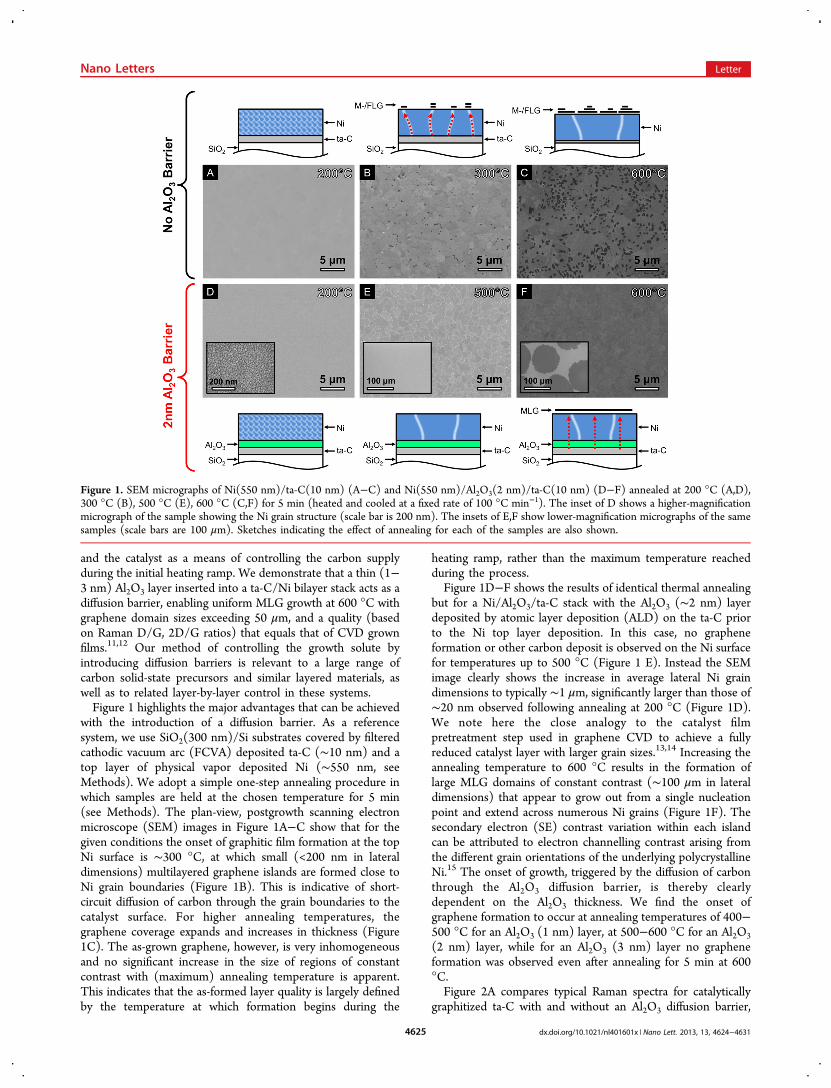
with the introduction of a diffusion barrier. As a referencesystem, we use SiO2(300 nm)/Si substrates covered by filteredcathodic vacuum arc (FCVA) deposited ta-C (∼10 nm) and atop layer of physical vapor deposited Ni (∼550 nm, seeMethods). We adopt a simple one-step annealing procedure inwhich samples are held at the chosen temperature for 5 min(see Methods). The plan-view, postgrowth scanning electronmicroscope (SEM) images in Figure 1A−C show that for thegiven conditions the onset of graphitic film formation at the topNi surface is ∼300 °C, at which small (<200 nm in lateraldimensions) multilayered graphene islands are formed close toNi grain boundaries (Figure 1B). This is indicative of short-circuit diffusion of carbon through the grain boundaries to thecatalyst surface. For higher annealing temperatures, thegraphene coverage expands and increases in thickness (Figure1C). The as-grown graphene, however, is very inhomogeneousand no significant increase in the size of regions of constantcontrast with (maximum) annealing temperature is apparent.This indicates that the as-formed layer quality is largely definedby the temperature at which formation begins during the
heating ramp, rather than the maximum temperature reachedduring the process.Figure 1D−F shows the results of identical thermal annealing
but for a Ni/Al2O3/ta-C stack with the Al2O3 (∼2 nm) layerdeposited by atomic layer deposition (ALD) on the ta-C priorto the Ni top layer deposition. In this case, no grapheneformation or other carbon deposit is observed on the Ni surfacefor temperatures up to 500 °C (Figure 1 E). Instead the SEMimage clearly shows the increase in average lateral Ni graindimensions to typically ∼1 μm, significantly larger than those of∼20 nm observed following annealing at 200 °C (Figure 1D).We note here the close analogy to the catalyst filmpretreatment step used in graphene CVD to achieve a fullyreduced catalyst layer with larger grain sizes.13,14 Increasing theannealing temperature to 600 °C results in the formation oflarge MLG domains of constant contrast (∼100 μm in lateraldimensions) that appear to grow out from a single nucleationpoint and extend across numerous Ni grains (Figure 1F). Thesecondary electron (SE) contrast variation within each islandcan be attributed to electron channelling contrast arising fromthe different grain orientations of the underlying polycrystallineNi.15 The onset of growth, triggered by the diffusion of carbonthrough the Al2O3 diffusion barrier, is thereby clearlydependent on the Al2O3 thickness. We find the onset ofgraphene formation to occur at annealing temperatures of 400−500 °C for an Al2O3 (1 nm) layer, at 500−600 °C for an Al2O3(2 nm) layer, while for an Al2O3 (3 nm) layer no grapheneformation was observed even after annealing for 5 min at 600°C.Figure 2A compares typical Raman spectra for catalytically
graphitized ta-C with and without an Al2O3 diffusion barrier,
Figure 1. SEM micrographs of Ni(550 nm)/ta-C(10 nm) (A−C) and Ni(550 nm)/Al2O3(2 nm)/ta-C(10 nm) (D−F) annealed at 200 °C (A,D),300 °C (B), 500 °C (E), 600 °C (C,F) for 5 min (heated and cooled at a fixed rate of 100 °C min−1). The inset of D shows a higher-magnificationmicrograph of the sample showing the Ni grain structure (scale bar is 200 nm). The insets of E,F show lower-magnification micrographs of the samesamples (scale bars are 100 μm). Sketches indicating the effect of annealing for each of the samples are also shown.
Nano Letters Letter
dx.doi.org/10.1021/nl401601x | Nano Lett. 2013, 13, 4624−46314625
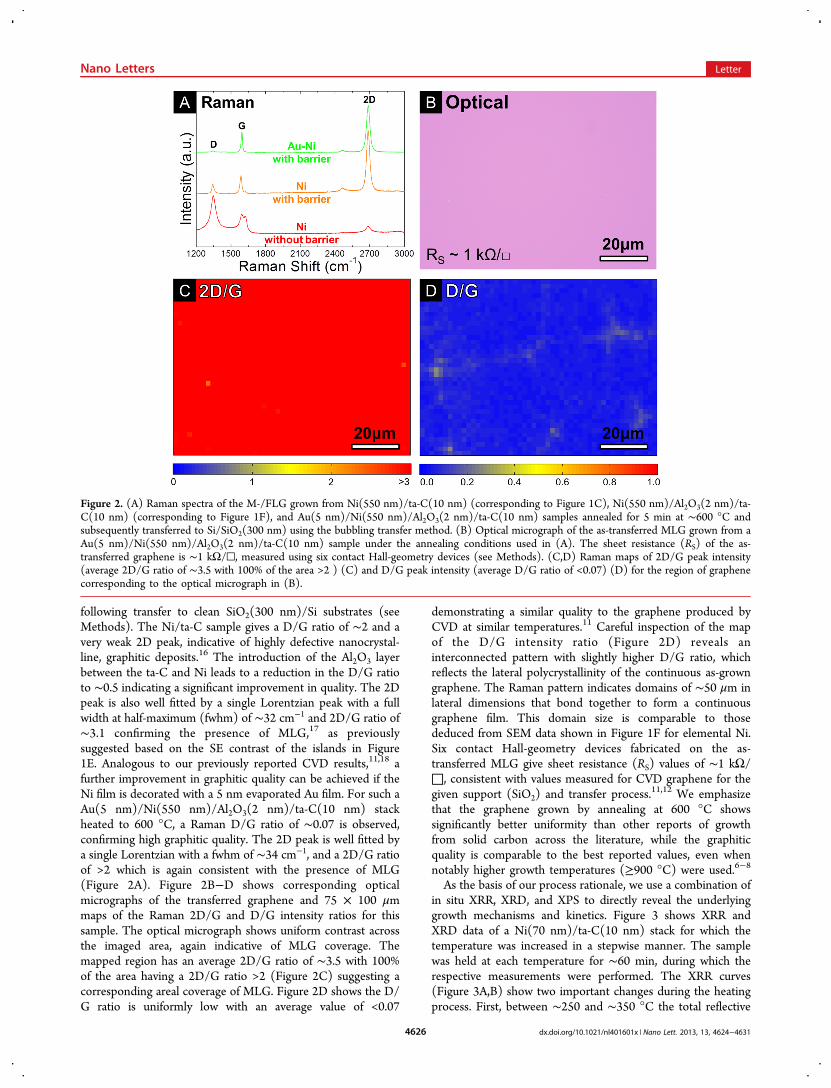
following transfer to clean SiO2(300 nm)/Si substrates (seeMethods). The Ni/ta-C sample gives a D/G ratio of ∼2 and avery weak 2D peak, indicative of highly defective nanocrystal-line, graphitic deposits.16 The introduction of the Al2O3 layerbetween the ta-C and Ni leads to a reduction in the D/G ratioto ∼0.5 indicating a significant improvement in quality. The 2Dpeak is also well fitted by a single Lorentzian peak with a fullwidth at half-maximum (fwhm) of ∼32 cm−1 and 2D/G ratio of∼3.1 confirming the presence of MLG,17 as previouslysuggested based on the SE contrast of the islands in Figure1E. Analogous to our previously reported CVD results,11,18 afurther improvement in graphitic quality can be achieved if theNi film is decorated with a 5 nm evaporated Au film. For such aAu(5 nm)/Ni(550 nm)/Al2O3(2 nm)/ta-C(10 nm) stackheated to 600 °C, a Raman D/G ratio of ∼0.07 is observed,confirming high graphitic quality. The 2D peak is well fitted bya single Lorentzian with a fwhm of ∼34 cm−1, and a 2D/G ratioof >2 which is again consistent with the presence of MLG(Figure 2A). Figure 2B−D shows corresponding opticalmicrographs of the transferred graphene and 75 × 100 μmmaps of the Raman 2D/G and D/G intensity ratios for thissample. The optical micrograph shows uniform contrast acrossthe imaged area, again indicative of MLG coverage. Themapped region has an average 2D/G ratio of ∼3.5 with 100%of the area having a 2D/G ratio >2 (Figure 2C) suggesting acorresponding areal coverage of MLG. Figure 2D shows the D/G ratio is uniformly low with an average value of <0.07
demonstrating a similar quality to the graphene produced byCVD at similar temperatures.11 Careful inspection of the mapof the D/G intensity ratio (Figure 2D) reveals aninterconnected pattern with slightly higher D/G ratio, whichreflects the lateral polycrystallinity of the continuous as-growngraphene. The Raman pattern indicates domains of ∼50 μm inlateral dimensions that bond together to form a continuousgraphene film. This domain size is comparable to thosededuced from SEM data shown in Figure 1F for elemental Ni.Six contact Hall-geometry devices fabricated on the as-transferred MLG give sheet resistance (RS) values of ∼1 kΩ/□, consistent with values measured for CVD graphene for thegiven support (SiO2) and transfer process.11,12 We emphasizethat the graphene grown by annealing at 600 °C showssignificantly better uniformity than other reports of growthfrom solid carbon across the literature, while the graphiticquality is comparable to the best reported values, even whennotably higher growth temperatures (≥900 °C) were used.6−8
As the basis of our process rationale, we use a combination ofin situ XRR, XRD, and XPS to directly reveal the underlyinggrowth mechanisms and kinetics. Figure 3 shows XRR andXRD data of a Ni(70 nm)/ta-C(10 nm) stack for which thetemperature was increased in a stepwise manner. The samplewas held at each temperature for ∼60 min, during which therespective measurements were performed. The XRR curves(Figure 3A,B) show two important changes during the heatingprocess. First, between ∼250 and ∼350 °C the total reflective
Figure 2. (A) Raman spectra of the M-/FLG grown from Ni(550 nm)/ta-C(10 nm) (corresponding to Figure 1C), Ni(550 nm)/Al2O3(2 nm)/ta-C(10 nm) (corresponding to Figure 1F), and Au(5 nm)/Ni(550 nm)/Al2O3(2 nm)/ta-C(10 nm) samples annealed for 5 min at ∼600 °C andsubsequently transferred to Si/SiO2(300 nm) using the bubbling transfer method. (B) Optical micrograph of the as-transferred MLG grown from aAu(5 nm)/Ni(550 nm)/Al2O3(2 nm)/ta-C(10 nm) sample under the annealing conditions used in (A). The sheet resistance (RS) of the as-transferred graphene is ∼1 kΩ/□, measured using six contact Hall-geometry devices (see Methods). (C,D) Raman maps of 2D/G peak intensity(average 2D/G ratio of ∼3.5 with 100% of the area >2 ) (C) and D/G peak intensity (average D/G ratio of <0.07) (D) for the region of graphenecorresponding to the optical micrograph in (B).
Nano Letters Letter
dx.doi.org/10.1021/nl401601x | Nano Lett. 2013, 13, 4624−46314626
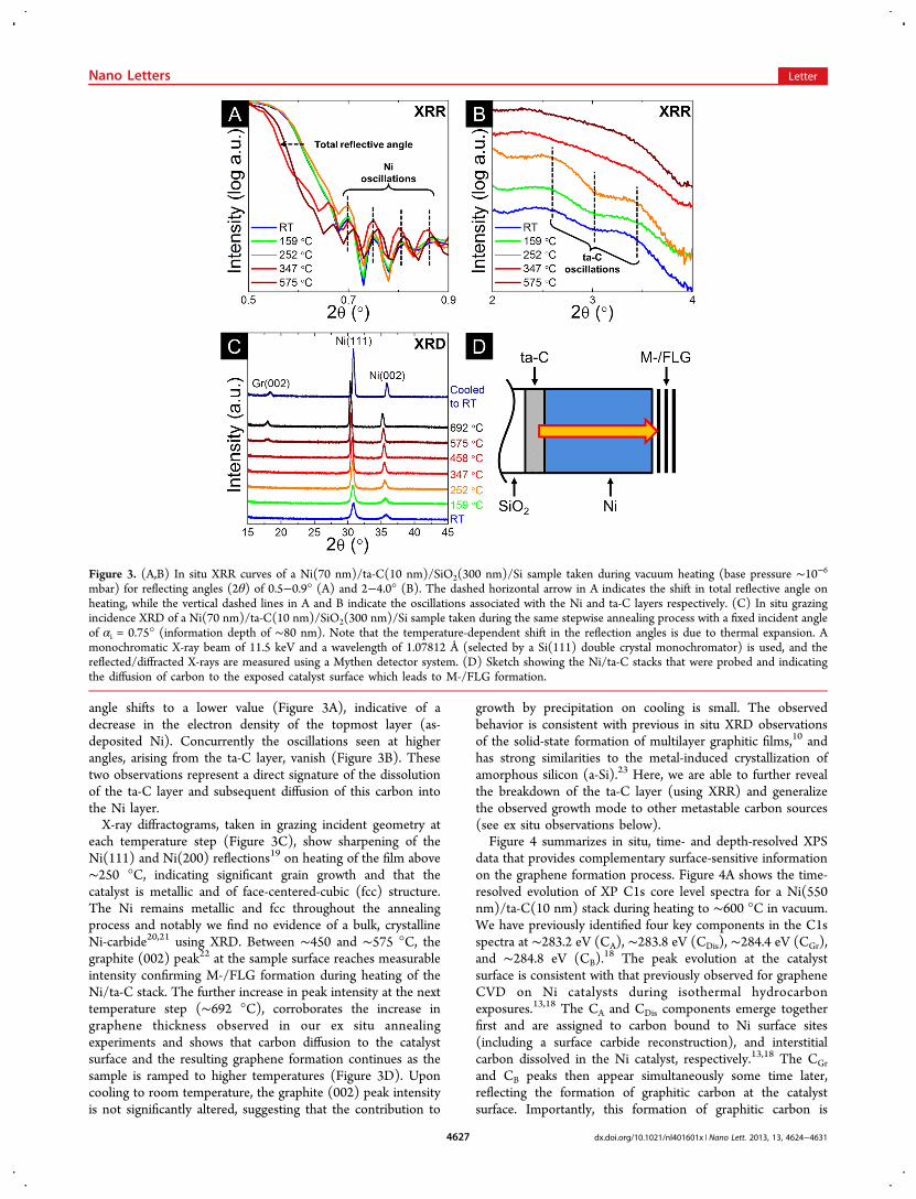
angle shifts to a lower value (Figure 3A), indicative of adecrease in the electron density of the topmost layer (as-deposited Ni). Concurrently the oscillations seen at higherangles, arising from the ta-C layer, vanish (Figure 3B). Thesetwo observations represent a direct signature of the dissolutionof the ta-C layer and subsequent diffusion of this carbon intothe Ni layer.X-ray diffractograms, taken in grazing incident geometry at
each temperature step (Figure 3C), show sharpening of theNi(111) and Ni(200) reflections19 on heating of the film above∼250 °C, indicating significant grain growth and that thecatalyst is metallic and of face-centered-cubic (fcc) structure.The Ni remains metallic and fcc throughout the annealingprocess and notably we find no evidence of a bulk, crystallineNi-carbide20,21 using XRD. Between ∼450 and ∼575 °C, thegraphite (002) peak22 at the sample surface reaches measurableintensity confirming M-/FLG formation during heating of theNi/ta-C stack. The further increase in peak intensity at the nexttemperature step (∼692 °C), corroborates the increase ingraphene thickness observed in our ex situ annealingexperiments and shows that carbon diffusion to the catalystsurface and the resulting graphene formation continues as thesample is ramped to higher temperatures (Figure 3D). Uponcooling to room temperature, the graphite (002) peak intensityis not significantly altered, suggesting that the contribution to
growth by precipitation on cooling is small. The observedbehavior is consistent with previous in situ XRD observationsof the solid-state formation of multilayer graphitic films,10 andhas strong similarities to the metal-induced crystallization ofamorphous silicon (a-Si).23 Here, we are able to further revealthe breakdown of the ta-C layer (using XRR) and generalizethe observed growth mode to other metastable carbon sources(see ex situ observations below).Figure 4 summarizes in situ, time- and depth-resolved XPS
data that provides complementary surface-sensitive informationon the graphene formation process. Figure 4A shows the time-resolved evolution of XP C1s core level spectra for a Ni(550nm)/ta-C(10 nm) stack during heating to ∼600 °C in vacuum.We have previously identified four key components in the C1sspectra at ∼283.2 eV (CA), ∼283.8 eV (CDis), ∼284.4 eV (CGr),and ∼284.8 eV (CB).
18 The peak evolution at the catalystsurface is consistent with that previously observed for grapheneCVD on Ni catalysts during isothermal hydrocarbonexposures.13,18 The CA and CDis components emerge togetherfirst and are assigned to carbon bound to Ni surface sites(including a surface carbide reconstruction), and interstitialcarbon dissolved in the Ni catalyst, respectively.13,18 The CGr
and CB peaks then appear simultaneously some time later,reflecting the formation of graphitic carbon at the catalystsurface. Importantly, this formation of graphitic carbon is
Figure 3. (A,B) In situ XRR curves of a Ni(70 nm)/ta-C(10 nm)/SiO2(300 nm)/Si sample taken during vacuum heating (base pressure ∼10−6mbar) for reflecting angles (2θ) of 0.5−0.9° (A) and 2−4.0° (B). The dashed horizontal arrow in A indicates the shift in total reflective angle onheating, while the vertical dashed lines in A and B indicate the oscillations associated with the Ni and ta-C layers respectively. (C) In situ grazingincidence XRD of a Ni(70 nm)/ta-C(10 nm)/SiO2(300 nm)/Si sample taken during the same stepwise annealing process with a fixed incident angleof αi = 0.75° (information depth of ∼80 nm). Note that the temperature-dependent shift in the reflection angles is due to thermal expansion. Amonochromatic X-ray beam of 11.5 keV and a wavelength of 1.07812 Å (selected by a Si(111) double crystal monochromator) is used, and thereflected/diffracted X-rays are measured using a Mythen detector system. (D) Sketch showing the Ni/ta-C stacks that were probed and indicatingthe diffusion of carbon to the exposed catalyst surface which leads to M-/FLG formation.
Nano Letters Letter
dx.doi.org/10.1021/nl401601x | Nano Lett. 2013, 13, 4624−46314627
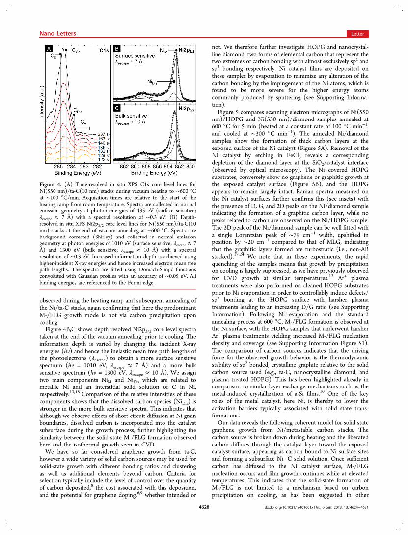
observed during the heating ramp and subsequent annealing ofthe Ni/ta-C stacks, again confirming that here the predominantM-/FLG growth mode is not via carbon precipitation uponcooling.Figure 4B,C shows depth resolved Ni2p3/2 core level spectra
taken at the end of the vacuum annealing, prior to cooling. Theinformation depth is varied by changing the incident X-rayenergies (hv) and hence the inelastic mean free path lengths ofthe photoelectrons (λescape) to obtain a more surface sensitivespectrum (hv = 1010 eV, λescape ≈ 7 Å) and a more bulksensitive spectrum (hv = 1300 eV, λescape ≈ 10 Å). We assigntwo main components NiM and NiDis which are related tometallic Ni and an interstitial solid solution of C in Ni,respectively.13,18 Comparison of the relative intensities of thesecomponents shows that the dissolved carbon species (NiDis) isstronger in the more bulk sensitive spectra. This indicates thatalthough we observe effects of short-circuit diffusion at Ni grainboundaries, dissolved carbon is incorporated into the catalystsubsurface during the growth process, further highlighting thesimilarity between the solid-state M-/FLG formation observedhere and the isothermal growth seen in CVD.We have so far considered graphene growth from ta-C,
however a wide variety of solid carbon sources may be used forsolid-state growth with different bonding ratios and clusteringas well as additional elements beyond carbon. Criteria forselection typically include the level of control over the quantityof carbon deposited,8 the cost associated with this deposition,and the potential for graphene doping,6,9 whether intended or
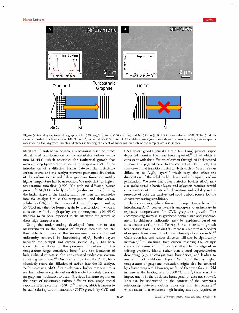
not. We therefore further investigate HOPG and nanocrystal-line diamond, two forms of elemental carbon that represent thetwo extremes of carbon bonding with almost exclusively sp2 andsp3 bonding respectively. Ni catalyst films are deposited onthese samples by evaporation to minimize any alteration of thecarbon bonding by the impingement of the Ni atoms, which isfound to be more severe for the higher energy atomscommonly produced by sputtering (see Supporting Informa-tion).Figure 5 compares scanning electron micrographs of Ni(550
nm)/HOPG and Ni(550 nm)/diamond samples annealed at600 °C for 5 min (heated at a constant rate of 100 °C min−1,and cooled at ∼300 °C min−1). The annealed Ni/diamondsamples show the formation of thick carbon layers at theexposed surface of the Ni catalyst (Figure 5A). Removal of theNi catalyst by etching in FeCl3 reveals a correspondingdepletion of the diamond layer at the SiO2/catalyst interface(observed by optical microscopy). The Ni covered HOPGsubstrates, conversely show no graphene or graphitic growth atthe exposed catalyst surface (Figure 5B), and the HOPGappears to remain largely intact. Raman spectra measured onthe Ni catalyst surfaces further confirms this (see insets) withthe presence of D, G, and 2D peaks on the Ni/diamond sampleindicating the formation of a graphitic carbon layer, while nopeaks related to carbon are observed on the Ni/HOPG sample.The 2D peak of the Ni/diamond sample can be well fitted witha single Lorentzian peak of ∼79 cm−1 width, upshifted inposition by ∼20 cm−1 compared to that of MLG, indicatingthat the graphitic layers formed are turbostratic (i.e., non-ABstacked).17,24 We note that in these experiments, the rapidquenching of the samples means that growth by precipitationon cooling is largely suppressed, as we have previously observedfor CVD growth at similar temperatures.13 Ar+ plasmatreatments were also performed on cleaned HOPG substratesprior to Ni evaporation in order to controllably induce defects/sp3 bonding at the HOPG surface with harsher plasmatreatments leading to an increasing D/G ratio (see SupportingInformation). Following Ni evaporation and the standardannealing process at 600 °C, M-/FLG formation is observed atthe Ni surface, with the HOPG samples that underwent harsherAr+ plasma treatments yielding increased M-/FLG nucleationdensity and coverage (see Supporting Information Figure S1).The comparison of carbon sources indicates that the drivingforce for the observed growth behavior is the thermodynamicstability of sp2 bonded, crystalline graphite relative to the solidcarbon source used (e.g., ta-C, nanocrystalline diamond, andplasma treated HOPG). This has been highlighted already incomparison to similar layer exchange mechanisms such as themetal-induced crystallization of a-Si films.10 One of the keyroles of the metal catalyst, here Ni, is thereby to lower theactivation barriers typically associated with solid state trans-formations.Our data reveals the following coherent model for solid-state
graphene growth from Ni/metastable carbon stacks. Thecarbon source is broken down during heating and the liberatedcarbon diffuses through the catalyst layer toward the exposedcatalyst surface, appearing as carbon bound to Ni surface sitesand forming a subsurface Ni−C solid solution. Once sufficientcarbon has diffused to the Ni catalyst surface, M-/FLGnucleation occurs and film growth continues while at elevatedtemperatures. This indicates that the solid-state formation ofM-/FLG is not limited to a mechanism based on carbonprecipitation on cooling, as has been suggested in other
Figure 4. (A) Time-resolved in situ XPS C1s core level lines forNi(550 nm)/ta-C(10 nm) stacks during vacuum heating to ∼600 °Cat ∼100 °C/min. Acquisition times are relative to the start of theheating ramp from room temperature. Spectra are collected in normalemission geometry at photon energies of 435 eV (surface sensitive;λescape ≈ 7 Å) with a spectral resolution of ∼0.3 eV. (B) Depth-resolved in situ XPS Ni2p3/2 core level lines for Ni(550 nm)/ta-C(10nm) stacks at the end of vacuum annealing at ∼600 °C. Spectra arebackground corrected (Shirley) and collected in normal emissiongeometry at photon energies of 1010 eV (surface sensitive; λescape ≈ 7Å) and 1300 eV (bulk sensitive; λescape ≈ 10 Å) with a spectralresolution of ∼0.3 eV. Increased information depth is achieved usinghigher-incident X-ray energies and hence increased electron mean freepath lengths. The spectra are fitted using Doniach-Sunjic functionsconvoluted with Gaussian profiles with an accuracy of ∼0.05 eV. Allbinding energies are referenced to the Fermi edge.
Nano Letters Letter
dx.doi.org/10.1021/nl401601x | Nano Lett. 2013, 13, 4624−46314628
literature.2−7 Instead we observe a mechanism based on directNi-catalyzed transformation of the metastable carbon sourceinto M-/FLG, which resembles the isothermal growth thatoccurs during hydrocarbon exposure for graphene CVD.18 Theintroduction of a diffusion barrier between the metastablecarbon source and the catalyst prevents premature dissolutionof the carbon source and delays graphene formation until ahigher temperature has been reached. We note that for higher-temperature annealing (>900 °C) with no diffusion barrierpresent,6,7 M-/FLG is likely to form (as discussed here) duringthe initial stages of the heating ramp, but then can redissolveinto the catalyst film as the temperature (and thus carbonsolubility of Ni) is further increased. Upon subsequent cooling,M-/FLG may then be formed again by precipitation,10 which isconsistent with the high-quality, yet inhomogeneous M-/FLGthat has so far been reported in the literature for growth atthese high temperatures.Using the understanding developed from our in situ
measurements in the context of existing literature, we arethus able to rationalize the improvement in quality anduniformity achieved by introducing Al2O3 barrier layersbetween the catalyst and carbon source. Al2O3 has beenshown to be stable in the presence of carbon for thetemperature range considered here,25 and the formation ofbulk nickel-aluminate is also not expected under our vacuumannealing conditions.26 Our results show that the Al2O3 filmseffectively retard the diffusion of carbon into the Ni catalyst.With increasing Al2O3 film thickness, a higher temperature isreached before adequate carbon diffuses to the catalyst surfacefor graphene nucleation to occur. Previous literature reports onthe onset of measurable carbon diffusion into single crystalsapphire at temperatures >500 °C.27 Further, Al2O3 is known tobe stable during carbon nanotube (CNT) growth by CVD and
CNT forest growth beneath a thin (∼10 nm) physical vapordeposited alumina layer has been reported,28 all of which isconsistent with the diffusion of carbon through ALD depositedalumina as suggested here. In the context of CNT CVD, it isalso known that transition metal catalysts such as Ni and Fe candiffuse in to Al2O3 layers29 which may also affect thedissociation of the solid carbon layer and subsequent carbonpermeation. We note that other materials besides Al2O3 mayalso make suitable barrier layers and selection requires carefulconsideration of the material’s deposition and stability in thepresence of both the catalyst and solid carbon source for thechosen processing conditions.The increase in graphene formation temperature achieved by
introducing Al2O3 barrier layers is analogous to an increase inexposure temperature for CVD graphene growth. Theaccompanying increase in graphene domain size and improve-ment in thickness uniformity may be explained based onconsiderations of carbon diffusivity. For an increase in growthtemperature from 300 to 600 °C, there is a more than 5 ordersof magnitude increase in the lattice diffusivity of carbon in Ni.30
Grain boundary and surface diffusion will also be significantlyincreased,31−33 meaning that carbon reaching the catalystsurface can more easily diffuse and attach to the edge of anexisting graphene island, rather than a local supersaturationdeveloping (e.g., at catalyst grain boundaries) and leading tonucleation of additional layers. We note that a highertemperature of graphene nucleation might also be achievedby a faster ramp rate. However, we found that even for a 10-foldincrease in the heating rate to 1000 °C min−1, there was littleimprovement in the thickness homogeneity (data not shown).This can be understood in the context of the Arrheniusrelationship between carbon diffusivity and temperature,30
which means that extremely high heating rates are required to
Figure 5. Scanning electron micrographs of Ni(550 nm)/diamond(∼100 nm) (A) and Ni(550 nm)/HOPG (B) annealed at ∼600 °C for 5 min invacuum (heated at a fixed rate of 100 °C min−1, cooled at ∼300 °C min−1). All scalebars are 2 μm. Insets show the corresponding Raman spectrameasured on the as-grown samples. Sketches indicating the effect of annealing on each of the samples are also shown.
Nano Letters Letter
dx.doi.org/10.1021/nl401601x | Nano Lett. 2013, 13, 4624−46314629
significantly increase the M-/FLG formation temperaturewithout a barrier layer.A key feature of our solid-state growth, is that M-/FLG
formation is fed from below the catalyst surface, therefore theformation of additional graphene layers is not limited by thealready formed graphene layers (and leakage of carbonprecursor through these), in contrast to CVD.11,12 Thethickness of FLG films instead may be defined prior to theannealing process by the quantity of solid carbon sourcedeposited. We note that throughout our experiments, thickerFLG regions generally showed lower D/G ratios compared toMLG regions, indicating that the additional layers formed havelower defect densities (compare, for example, the growth fromelemental Ni in Figures 2A and 5A). This may relate to theseadditional layers forming once the catalyst has reached a highertemperature due to continued carbon diffusion to the catalystsurface. These additional layers were also found to beturbostratic with 2D peaks well fitted by single Lorentzianpeaks but with fwhm of >40 cm−1.17,24 This is in contrast to theBernal stacked graphene formed during CVD on Ni-basedcatalysts11 and may relate to a more rapid feeding of carbon tothe catalyst surface from the underlying solid source, or adifferent distribution of dissolved carbon within the catalyst,34
arising from the way in which carbon is supplied.In summary, we establish the introduction of carbon
diffusion barriers as a general and simple method to controland improve graphene formation from the catalytic trans-formation of solid carbon sources. We focus on (Au-alloyed) Niatop ta-C, nanocrystalline diamond, and plasma-treated HOPGas model systems to highlight via complementary in situ XRR,XRD, and XPS measurements that graphene growth fortechnologically relevant low temperatures (<600 °C) occurspredominantly during ramping up and annealing by carbondissolution and diffusion through the catalyst, driven by thethermodynamic stability of graphene. This is also relevant forhigher temperature annealing, for which an additionalredissolution of as-formed graphene might occur. Hence akey problem with solid-state graphene growth, relevant to allprevious literature, is the lack of an “on-switch” for the carbonsupply. We address this key problem by introducing a diffusionbarrier between the solid carbon source and the catalyst, here inthe form of a nanometer-thick Al2O3 layer, which effectivelyprevents premature carbon dissolution and allows us todemonstrate a significantly improved M-/FLG quality anduniformity comparable to that achieved by CVD. We note thatM-/FLG growth from solid carbon sources is a scalabletechnique,35 and importantly offers a route for the directintegration of graphene in device architectures.14 We expect ourmethod of controlling the growth by introducing diffusionbarriers to be relevant to a large range of carbon solid-stateprecursors and similar layered materials, as well as to relatedlayer-by-layer control in these systems.Methods. We investigate polycrystalline Ni films (550 nm
thick unless otherwise stated) thermally evaporated, orsputtered onto various substrates chosen to act as solid carbonsources: highly orientated pyrolytic graphite (HOPG),tetrahedral amorphous carbon (ta-C), and nanocrystallinediamond. HOPG(0001) substrates (Mikromasch, ZYH grade,< 3.5° mosaic spread) are cleaved to ∼0.1 mm thickness andthe surfaces cleaned by mechanical exfoliation using the well-established scotch-tape method. Ta−C was deposited on toSiO2(300 nm)/Si substrates using a filtered cathodic vacuumarc (FCVA) system. Nanocrystalline diamond films (∼100 nm
thick) were deposited on SiO2(500 nm)/Si substrates usingmicrowave plasma enhanced CVD.36 Al2O3 (1−3 nm) layersare deposited by atomic layer deposition using a CambridgeNanotech Savannah ALD system with a 200 °C process thatuses tri[methyl]aluminium as a precursor and water as anoxidant both carried in a N2(20 sccm) flow for 10−30cycles.37,38 For the Au decorated Ni catalysts, Au(5 nm) wasdeposited by thermal evaporation on to the exposed Ni surface.The samples are annealed under vacuum in a custom-built cold-wall reactor at selected temperatures using a standard one stepprocedure [<10−6 mbar, 200−600 °C, 5 min, heated and cooledat a constant rate of 100 °C min−1] unless otherwise stated.In situ high-pressure XPS measurements during vacuum
annealing were performed at the BESSY II synchrotron at theISISS end station of the FHI-MPG. In situ XRR and (grazingincidence) XRD were performed during vacuum annealing atthe European Synchrotron Radiation Facility (beamline BM20/ROBL, operated by the Helmholtz-Zentrum Dresden-Rossendorf). Ex situ characterization is performed on as-grown samples using scanning electron microscopy (SEM,Zeiss SigmaVP, 1 kV) or after transfer of the M-/FLG films toSiO2(300 nm)/Si substrates using optical microscopy, andRaman spectroscopy (Renishaw Raman InVia Microscope, 532nm excitation). Transfer to SiO2(300 nm)/Si substrates iscarried out using an electrolysis-based bubbling in a NaOH (1M) aqueous solution to detach PMMA-supported graphenefrom the catalyst,39,40 with the PMMA subsequently removedin acetone. Electrical measurements are performed at roomtemperature using six contact Hall-geometry devices fabricatedby e-beam lithography on the as-transferred MLG. Cr/Aucontacts are evaporated on top of the MLG which is thenpatterned by an O2 plasma etch.
■ ASSOCIATED CONTENT
*S Supporting InformationControlled HOPG plasma damage experiments. This materialis available free of charge via the Internet at http://pubs.acs.org.
■ AUTHOR INFORMATION
Corresponding Author*E-mail [email protected].
NotesThe authors declare no competing financial interest.
■ ACKNOWLEDGMENTS
We are grateful to Stephen Fleming for assistance with e-beamlithography. We also thank Dr. Oliver A. Williams for providingthe nanocrystalline diamond films used in this work. R.S.W.acknowledges funding from EPSRC (Doctoral training award)and Sidney Sussex College. S.H. acknowledges funding fromERC Grant InsituNANO (279342). P.R.K. acknowledgesfunding from the Cambridge Commonwealth Trust. Thisresearch was partially supported by the EUFP7 WorkProgramme under grant GRAFOL (project reference285275), and EPSRC under Grant GRAPHTED (projectreference EP/K016636/1) and Grant EP/H047565/1. Weacknowledge the Helmholtz-Zentrum-Berlin Electron storagering BESSY II for provision of synchrotron radiation at theISISS beamline and we thank the BESSY staff for continuoussupport of our experiments. We acknowledge the EuropeanSynchrotron Radiation Facility (ESRF) for provision of
Nano Letters Letter
dx.doi.org/10.1021/nl401601x | Nano Lett. 2013, 13, 4624−46314630
synchrotron radiation and we thank the staff for assistance inusing beamline BM20/ROBL.
■ REFERENCES(1) Novoselov, K. S.; Fal’ko, V. I.; Colombo, L.; Gellert, P. R.;Schwab, M. G.; Kim, K. Nature 2012, 490, 192−200.(2) Zheng, M.; Takei, K.; Hsia, B.; Fang, H.; Zhang, X.; Ferralis, N.;Ko, H.; Chueh, Y.-L.; Zhang, Y.; Maboudian, R.; Javey, A. Appl. Phys.Lett. 2010, 96, 063110.(3) Hofrichter, J.; Szafranek, B. N.; Otto, M.; Echtermeyer, T. J.;Baus, M.; Majerus, A.; Geringer, V.; Ramsteiner, M.; Kurz, H. NanoLett. 2010, 10, 36−42.(4) Suzuki, S.; Takei, Y.; Furukawa, K.; Hibino, H. Appl. Phys. Express2011, 4, 065102.(5) García, J. M.; He, R.; Jiang, M. P.; Kim, P.; Pfeiffer, L. N.;Pinczuk, A. Carbon 2011, 49, 1006−1012.(6) Sun, Z.; Yan, Z.; Yao, J.; Beitler, E.; Zhu, Y.; Tour, J. M. Nature2010, 468, 549−552.(7) Peng, Z.; Yan, Z.; Sun, Z.; Tour, J. M. ACS Nano 2011, 5, 8241−8247.(8) Shin, H.-J.; Choi, W. M.; Yoon, S.-M.; Han, G. H.; Woo, Y. S.;Kim, E. S.; Chae, S. J.; Li, X.-S.; Benayad, A.; Loc, D. D.; Gunes, F.;Lee, Y. H.; Choi, J.-Y. Adv. Mater. 2011, 23, 4392−4397.(9) Xiong, W.; Zhou, Y. S.; Jiang, L. J.; Sarkar, A.; Mahjouri-Samani,M.; Xie, Z. Q.; Gao, Y.; Ianno, N. J.; Jiang, L.; Lu, Y. F. Adv. Mater.2013, 25, 630−634.(10) Saenger, K. L.; Tsang, J. C.; Bol, A. A.; Chu, J. O.; Grill, A.;Lavoie, C. Appl. Phys. Lett. 2010, 96, 153105.(11) Weatherup, R. S.; Dlubak, B.; Hofmann, S. ACS Nano 2012, 6,9996−10003.(12) Kidambi, P. R.; Ducati, C.; Dlubak, B.; Gardiner, D.; Weatherup,R. S.; Martin, M.-B.; Seneor, P.; Coles, H.; Hofmann, S. J. Phys. Chem.C 2012, 116, 22492−22501.(13) Weatherup, R. S.; Bayer, B. C.; Blume, R.; Baehtz, C.; Kidambi,P. R.; Fouquet, M.; Wirth, C. T.; Schlogl, R.; Hofmann, S.ChemPhysChem 2012, 13, 2544−2549.(14) Dlubak, B.; Martin, M.-B.; Weatherup, R. S.; Yang, H.; Deranlot,C.; Blume, R.; Schloegl, R.; Fert, A.; Anane, A.; Hofmann, S.; Seneor,P.; Robertson, J. ACS Nano 2012, 6, 10930−10934.(15) Goldstein, J.; Newbury, D. E.; Joy, D. C.; Lyman, C. E.; Echlin,P.; Lifshin, E.; Sawyer, L.; Michael, J. R. Scanning Electron Microscopyand X-Ray Microanalysis, 3rd ed.; Kluwer Academic Publishers: NewYork, 2003.(16) Ferrari, A.; Robertson, J. Phys. Rev. B 2000, 61, 14095−14107.(17) Ferrari, A.; Meyer, J.; Scardaci, V.; Casiraghi, C.; Lazzeri, M.;Mauri, F.; Piscanec, S.; Jiang, D.; Novoselov, K.; Roth, S.; Geim, A.Phys. Rev. Lett. 2006, 97, 187401.(18) Weatherup, R. S.; Bayer, B. C.; Blume, R.; Ducati, C.; Baehtz,C.; Schlogl, R.; Hofmann, S. Nano Lett. 2011, 11, 4154−4160.(19) Powder Diffraction File 04-0850. JCPDS-International Centre forDiffraction Data; Newtown Square, PA.(20) Powder Diffraction File 72-1467. JCPDS-International Centre forDiffraction Data; Newtown Square, PA.(21) Portnoi, V. K.; Leonov, A. V.; Mudretsova, S. N.; Fedotov, S. A.Phys. Metals Metallogr. 2010, 109, 153−161.(22) Powder Diffraction File 89-8487. JCPDS-International Centre forDiffraction Data; Newtown Square: PA.(23) Gosele, U. In Alloying; Walters, J. L., Jackson, H. R., Sims, C. T.,Eds.; ASM International: Metals Park, Ohio, 1988; pp 489−519.(24) Lespade, P.; Marchand, A.; Couzi, M.; Cruege, F. Carbon 1984,22, 375−385.(25) Halmann, M.; Frei, A.; Steinfeld, A. Miner. Process. Extr. Metall.Rev. 2011, 32, 247−266.(26) Trumble, K.; Ruhle, M. Acta Metall. Mater. 1991, 39, 1915−1924.(27) Guenette, M. C.; Tucker, M. D.; Ionescu, M.; Bilek, M. M. M.;McKenzie, D. R. J. Appl. Phys. 2011, 109, 083503.
(28) Yan, Z.; Ma, L.; Zhu, Y.; Lahiri, I.; Hahm, M.; Liu, Z.; Yang, S.;Xiang, C.; Lu, W.; Peng, Z.; Sun, Z.; Kittrell, C.; Lou, J.; Choi, W.;Ajayan, P. M.; Tour, J. M. ACS Nano 2013, 7, 58−64.(29) Amama, P. B.; Pint, C. L.; Kim, S. M.; McJilton, L.; Eyink, K. G.;Stach, E. A.; Hauge, R. H.; Maruyama, B. ACS Nano 2010, 4, 895−904.(30) Lander, J. J.; Kern, H. E.; Beach, A. L. J. Appl. Phys. 1952, 23,1305−1309.(31) Mishin, Y.; Herzig, C. Mater. Sci. Eng., A 1999, 260, 55−71.(32) Parthasarathy, T.; Shewmon, P. Scr. Metall. 1983, 17, 943−946.(33) Hofmann, S.; Csanyi, G.; Ferrari, A.; Payne, M.; Robertson, J.Phys. Rev. Lett. 2005, 95, 036101.(34) Rinaldi, A.; Tessonnier, J.-P.; Schuster, M. E.; Blume, R.;Girgsdies, F.; Zhang, Q.; Jacob, T.; Abd Hamid, S. B.; Su, D. S.;Schlogl, R. Angew. Chem., Int. Ed. 2011, 50, 3313−3317.(35) Sun, Z.; Yan, Z.; Yao, J.; Beitler, E.; Zhu, Y.; Tour, J. M. Nature2010, 468, 549−552.(36) Williams, O. A.; Kriele, A.; Hees, J.; Wolfer, M.; Muller-Sebert,W.; Nebel, C. E. Chem. Phys. Lett. 2010, 495, 84−89.(37) Dlubak, B.; Kidambi, P. R.; Weatherup, R. S.; Hofmann, S.;Robertson, J. Appl. Phys. Lett. 2012, 100, 173113.(38) Puurunen, R. L. J. Appl. Phys. 2005, 97, 121301.(39) Wang, H.; Taychatanapat, T.; Hsu, A. IEEE Electron Device Lett.2011, 32, 1209−1211.(40) Gao, L.; Ren, W.; Xu, H.; Jin, L.; Wang, Z.; Ma, T.; Ma, L.-P.;Zhang, Z.; Fu, Q.; Peng, L.-M.; Bao, X.; Cheng, H.-M. Nat. Commun.2012, 3, 699.
Nano Letters Letter
dx.doi.org/10.1021/nl401601x | Nano Lett. 2013, 13, 4624−46314631


![GLOBAL STABILITY AND UNIFORM PERSISTENCE …1701.01407v1 [math.AP] 5 Jan 2017 GLOBAL STABILITY AND UNIFORM PERSISTENCE OF THE REACTION-CONVECTION-DIFFUSION CHOLERA EPIDEMIC MODEL KAZUO](https://img.pdfslide.us/doc/110x75/5ad6051b7f8b9a0d2d8e67d7/global-stability-and-uniform-persistence-170101407v1-mathap-5-jan-2017-global.jpg)