Embed Size (px)
Citation preview

Zulfiqar Ali EEE132 1
Intrinsic Carrier Concentration
I. Definition Intrinsic semiconductor: A semiconductor material with no dopants. It electrical characteristics such as concentration of charge carriers, depend only on pure crystal.
II. To derive carrier concentration in thermal equilibrium condition that is in a steady state condition at a given temperature without any external excitation.
III. Practical an intrinsic semiconductor is one that contains relatively small amount of impurities.

Zulfiqar Ali EEE132 2
Intrinsic Carrier Concentration
I. To obtain the electron density (number of electron per unit volume) in intrinsic semiconductor , we must evaluate the electron density in an incremental energy range dE.
II. Density n(E) is given by product of density states N(E) and a probability of occupying energy range F(E).
III. Thus the electron density is given by:
∫ ∫==ETOP ETOP
dEEFENdEEnn0 0
)()()(

Zulfiqar Ali EEE132 3
Intrinsic Carrier Concentration
Where n is in cm-3 and N(E) is in (cm3-eV)-1.The probability that an electron occupies and electronic state with energy E is given by Fermi-Dirac distribution.
k is Boltzman constant, t is temperature( K), EFis Fermi level.
kTEE F
eEF )(
1
1)( −
+=

Zulfiqar Ali EEE132 4
Intrinsic Semiconductor
The Fermi energy is the energy at which the probability of occupation by an electron is exactly on half.

Zulfiqar Ali EEE132 5
Figure 2.20. Fermi distribution function F(E) versus (E – EF) for various temperatures.

Zulfiqar Ali EEE132 6
Figure 2.21. Intrinsic semiconductor. (a) Schematic band diagram. (b) Density of states. (c) Fermi distribution function. (d) Carrier concentration.

Zulfiqar Ali EEE132 7
Intrinsic Carrier Concentration
There are large number of allowed states in the conduction band.However there will not be many electrons in the conduction band.Therefore the possibility for the electron to be in region is very low.If we refer to the bottom of the conduction band the electron density is equivalent to

Zulfiqar Ali EEE132 8
Intrinsic semiconductor
Electron density in the conduction band.
NC = 2.86 X 1019cm-3 for silicon and 4.7 X 1017cm-3 for gallium arsenide.
NV = 2.66 X 1019cm-3 for silicon and 7 X 1018cm-3
for gallium arsenide
])(exp[ kTEENn FC
C−−=
])(exp[ kTEENp VF
V−−=

Zulfiqar Ali EEE132 9
Intrinsic Semiconductor
In intrinsic semiconductor the number of electron per unit volume is equal to number of hole per unit volume in the valence band.
The larger the band gap the smaller intrinsic carrier density.
2innp =

Zulfiqar Ali EEE132 10
Nondegenerated Semiconductor
For shallow donors in silicon there usually enough energy to ionize all donor impurities at room temp.This condition is called complete ionization.Therefore n = ND
EC-EF = kT ln (NC/ND)Same case applies to hole.

Zulfiqar Ali EEE132 11
Figure 2.26. n-Type semiconductor. (a) Schematic band diagram. (b) Density of states. (c) Fermi distribution function (d) Carrier concentration. Note
that np = ni2.

Zulfiqar Ali EEE132 12
Reading assignment read on the Degenerated Semiconductor

Zulfiqar Ali EEE132 13
Carrier Transport Phenomena (Carrier Drift)
MobilityElectrons move in all different direction.When small electric field E is applied to the semiconductor electron will experience force. –qE.The electron will accelerated along the field. In opposite direction.Additional component is called a drift velocity.

Zulfiqar Ali EEE132 14
Mobility
The momentum applied to an electron is momentum gained.
The drift velocity depend on the applied electric field.
ετ
ετ
⎟⎟⎠
⎞⎜⎜⎝
⎛−=
=−
n
Cn
nnc
mq
v
vmq

Zulfiqar Ali EEE132 15
Mobility
The proportionality factor is called electron mobility
Is important parameter in carrier transport because it describes how strongly the motion of electron in influenced by applied electric field.
n
cn m
qτμ ≡

Zulfiqar Ali EEE132 16
Mobility
Drift velocity
Hole flows in the same direction as electric field.The mobility is influenced by impurity scattering and lattice scattering.
εμεμ
pp
nn
vv
=−=

Zulfiqar Ali EEE132 17
Current
The transport carriers under the influence of an electric field produce drift current.

Zulfiqar Ali EEE132 18
Figure 3.5. Current conduction in a uniformly doped semiconductor bar with length
L and cross-sectional area A.

Zulfiqar Ali EEE132 19
Resistivity
Sample semiconductor of length L and cross section of A and an electron concentration of n electrons/cm3.If we apply an electric field to the sample the electron current density Jn flowing in the sample should be product of charge (-q) on electron time the electron velocity.
nn qnvJ −=
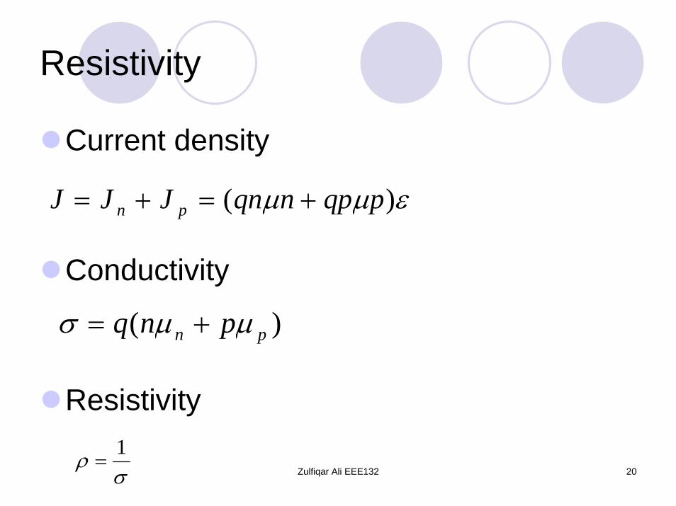
Zulfiqar Ali EEE132 20
Resistivity
Current density
Conductivity
Resistivity
εμμ )( pqpnqnJJJ pn +=+=
)( pn pnq μμσ +=
σρ 1=


![· Web viewSolid and Semiconductor devices & Communication Devices) 1 Give the ratio of number of holes and the number of conduction electrons in an intrinsic semiconductor. [1]](https://img.pdfslide.us/doc/110x75/5b7552367f8b9a924c8d3814/-web-viewsolid-and-semiconductor-devices-communication-devices-1-give-the.jpg)


![4-Lesson4-Intrinsic & Doped Semiconductor [Compatibility Mode]](https://img.pdfslide.us/doc/110x75/577d35001a28ab3a6b8f57a4/4-lesson4-intrinsic-doped-semiconductor-compatibility-mode.jpg)
