Embed Size (px)
Citation preview

P.Ravindran, PHY02E – Semiconductor Physics, 17 January 2014 : Carriers Concentration in Semiconductors - IV
http://folk.uio.no/ravi/semi2013
Prof.P. Ravindran, Department of Physics, Central University of Tamil
Nadu, India
Carriers Concentration in Semiconductors - IV
1

P.Ravindran, PHY02E – Semiconductor Physics, 17 January 2014 : Carriers Concentration in Semiconductors - IV
Bandgap Energy: Energy required to remove a valence electron and allow it to freely conduct.
Intrinsic Semiconductor: A “native semiconductor” with no dopants. Electrons in the
conduction band equal holes in the valence band. The concentration of
electrons (=holes) is the intrinsic concentration, ni.
Extrinsic Semiconductor: A doped semiconductor. Many electrical properties controlled by the
dopants, not the intrinsic semiconductor.
Donor: An impurity added to a semiconductor that adds an additional electron not found in
the native semiconductor.
Acceptor: An impurity added to a semiconductor that adds an additional hole not found in the
native semiconductor.
Dopant: Either an acceptor or donor.
N-type material: When electron concentrations (n=number of electrons/cm3) exceed the hole
concentration (normally through doping with donors).
P-type material: When hole concentrations (p=number of holes/cm3) exceed the electron
concentration (normally through doping with acceptors).
Majority carrier: The carrier that exists in higher population (i.e. n if n>p, p if p>n)
Minority carrier: The carrier that exists in lower population (i.e. n if n<p, p if p<n)
Summary of Important terms and symbols
P.Ravindran, PHY02E – Semiconductor Physics, 17 January 2014 : Carriers Concentration in Semiconductors - IV
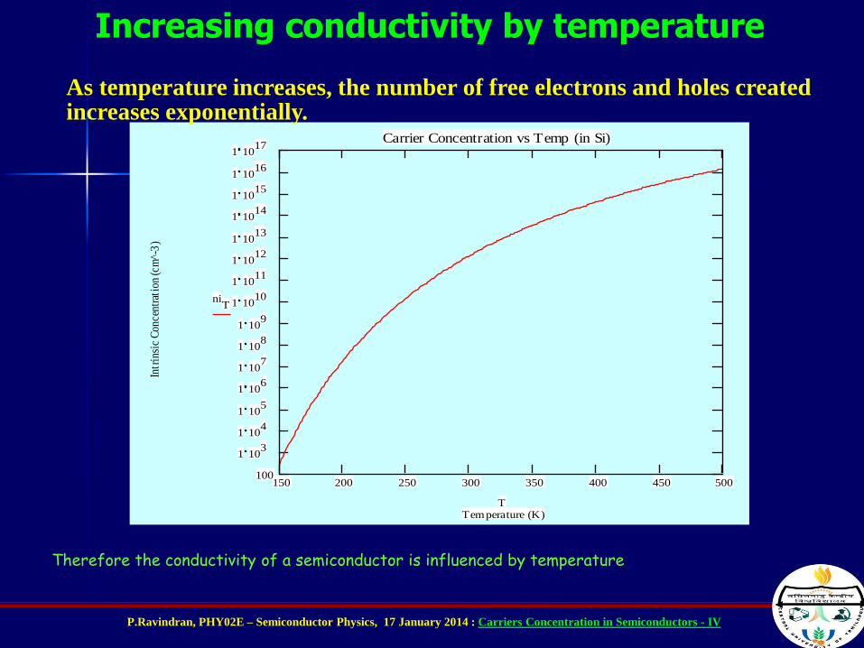
Increasing conductivity by temperature
150 200 250 300 350 400 450 500100
1 103
1 104
1 105
1 106
1 107
1 108
1 109
1 1010
1 1011
1 1012
1 1013
1 1014
1 1015
1 1016
1 1017
Carrier Concentration vs Temp (in Si)
Temperature (K)
Intr
insi
c C
once
ntra
tion
(cm
^-3
)
niT
T
Therefore the conductivity of a semiconductor is influenced by temperature
As temperature increases, the number of free electrons and holes created increases exponentially.
P.Ravindran, PHY02E – Semiconductor Physics, 17 January 2014 : Carriers Concentration in Semiconductors - IV
The conductivity of the semiconductor material increases when the temperature increases.
This is because the application of heat makes it possible for some electrons in the valence band to move to the conduction band.
Obviously the more heat applied the higher the number of electrons that can gain the required energy to make the conduction band transition and become available as charge carriers.
This is how temperature affects the carrier concentration.
Another way to increase the number of charge carriers is to add them in from an external source.
Doping or implant is the term given to a process whereby one element is injected with atoms of another element in order to change its properties.
Semiconductors (Si or Ge) are typically doped with elements such as Boron, Arsenic and Phosphorous to change and enhance their electrical properties.
Increasing conductivity

P.Ravindran, PHY02E – Semiconductor Physics, 17 January 2014 : Carriers Concentration in Semiconductors - IV
Extrinsic MaterialBy doping, a crystal can be altered so that it has a predominance of either
electrons or holes. Thus there are two types of doped semiconductors, n-type (mostly electrons) and p-type (mostly holes). When a crystal is doped such that the equilibrium carrier concentrations n0 and po are different from the intrinsic carrier concentration ni, the material is said to be
extrinsic.
Donor impurities (elements of
group V): P, Sb, As
Acceptor elements (group III):
B, Al, Ga, In
The valence and conduction bands of silicon
with additional impurity energy levels within
the energy gap.
When impurities or lattice defects are introduced, additional levels are created in the energy bands structure, usually within the band gap.
Total number of electrons
III – Al – 13
IV – Si – 14
V - P - 15

P.Ravindran, PHY02E – Semiconductor Physics, 17 January 2014 : Carriers Concentration in Semiconductors - IV
Extrinsic Material – donation of electrons
An impurity from column V introduces an energy level very near the conduction band in Ge or Si. This level is filled with electrons at 0 K, and very little thermal energy is required to excite these electrons to the conduction band. Thus, at about 50-100 K nearly all of the electrons in the impurity level are "donated" to the conduction band. Such an impurity level is called a donor level, and the column V impurities in Ge or Si are called donor impurities. From figure we note that the material doped with donor impurities can have a considerable concentration of electrons in the conduction band, even when the temperature is too low for the intrinsic EHP concentration to be appreciable. Thus semiconductors doped with a significant number of donor atoms will have n0>>(ni,p0) at room temperature. This is n-type material.
Donation of electrons from a donor
level to the conduction band
n-type material

P.Ravindran, PHY02E – Semiconductor Physics, 17 January 2014 : Carriers Concentration in Semiconductors - IV
Extrinsic Material – acceptance of electrons
Acceptance of valence band electrons by
an acceptor level, and the resulting
creation of holes.
Atoms from column III (B, Al, Ga, and In) introduce impurity levels in Ge or Si near the valence band. These levels are empty of electrons at 0 K. At low temperatures, enough thermal energy is available to excite electrons from the valence band into the impurity level, leaving behind holes in the valence band. Since this type of impurity level "accepts" electrons from the valence band, it is called an acceptor level, and the column III impurities are acceptor impurities in Ge and Si. As figure indicates, doping with acceptor impurities can create a semiconductor with a hole concentration p0 much greater than the conduction band electron concentration ni (this is p-type material).
P-type material

P.Ravindran, PHY02E – Semiconductor Physics, 17 January 2014 : Carriers Concentration in Semiconductors - IV
The motion of electrons in a crystal can be visualized and described in a
quasi-classical manner.
In most instances
The electron can be thought of as a particle.
The electronic motion can be modeled using Newtonian mechanics.
The effect of crystalline forces and quantum mechanical properties are
incorporated into the effective mass factor.
m* > 0 : near the bottoms of all bands
m* < 0 : near the tops of all bands
Carriers in a crystal with energies near the top or bottom of an energy
band typically exhibit a constant (energy-independent) effective mass.
` : near band edge
Effective Mass Approximation
constant2
2
dk
Ed

P.Ravindran, PHY02E – Semiconductor Physics, 17 January 2014 : Carriers Concentration in Semiconductors - IV
Effective Mass (I)
An electron moving in respond to an applied electric field.
E
E
within a Vacuum within a semiconductor crystal
dt
dvmEqF 0
dt
dvmEqF n
It allow us to conceive of electrons and holes as quasi-classical particles and to employ classical particle
relationships in semiconductor crystals or in most device analysis.
P.Ravindran, PHY02E – Semiconductor Physics, 17 January 2014 : Carriers Concentration in Semiconductors - IV
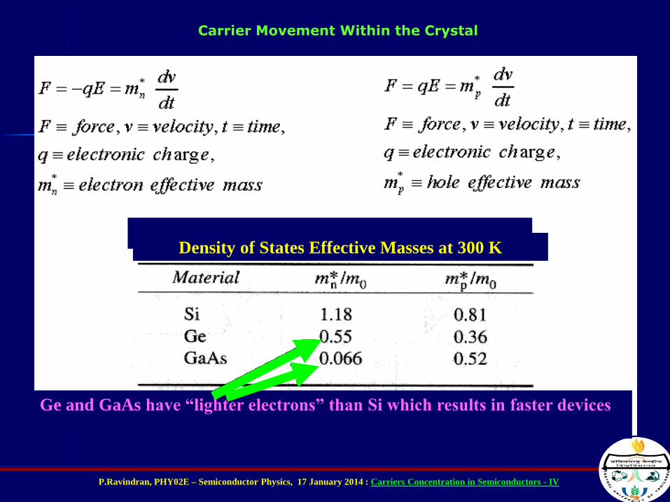
Carrier Movement Within the Crystal
Density of States Effective Masses at 300 K
Ge and GaAs have “lighter electrons” than Si which results in faster devices

P.Ravindran, PHY02E – Semiconductor Physics, 17 January 2014 : Carriers Concentration in Semiconductors - IV
Effective Mass (II)
Electrons are not free but interact with periodic potential of the lattice.
Wave-particle motion is not as same as in free space.
Curvature of the band determine m*.
m* is positive in CB min., negative in VB max.

P.Ravindran, PHY02E – Semiconductor Physics, 17 January 2014 : Carriers Concentration in Semiconductors - IV
Effective Masses
Curvature of the band determines the effective mass of the
carriers in a crystal, which is different from the free electron
mass.
Smaller curvature heavier mass
Larger curvature lighter mass
• For parabolic bands, the components of the effective mass
tensor are calculated according to:
jiijkk
E
m
2
2*
11
Si
*
*
*
*
100
01
0
001
1
zz
yy
xx
m
m
m
m

P.Ravindran, PHY02E – Semiconductor Physics, 17 January 2014 : Carriers Concentration in Semiconductors - IV
• From the knowledge of the energy band structure, one can construct the plot for the
allowed k-values associated with a given energy => constant energy surfaces
*
2
*
2
*
22
2ziyixi m
k
m
k
m
kEE zyx
iC
Si Ge
Note: The electron effective mass in GaAs is isotropic, which leads to spherically
symmetric constant energy surfaces.

P.Ravindran, PHY02E – Semiconductor Physics, 17 January 2014 : Carriers Concentration in Semiconductors - IV
Due to the p-like symmetry and mixing of the V.B. states, the constant energy surfaces
are warped spheres:
The hh-band is most warped
The lh- and so-band are more spherical
212222222422
2
2)( xzzyyx kkkkkkCkBAk
mkE
A
mm
CBA
mm
CBA
mm o
soo
lho
hh
*
22
*
22
*,
6/,
6/
Valence
bands
Constant energy
surfaces