Embed Size (px)
Citation preview
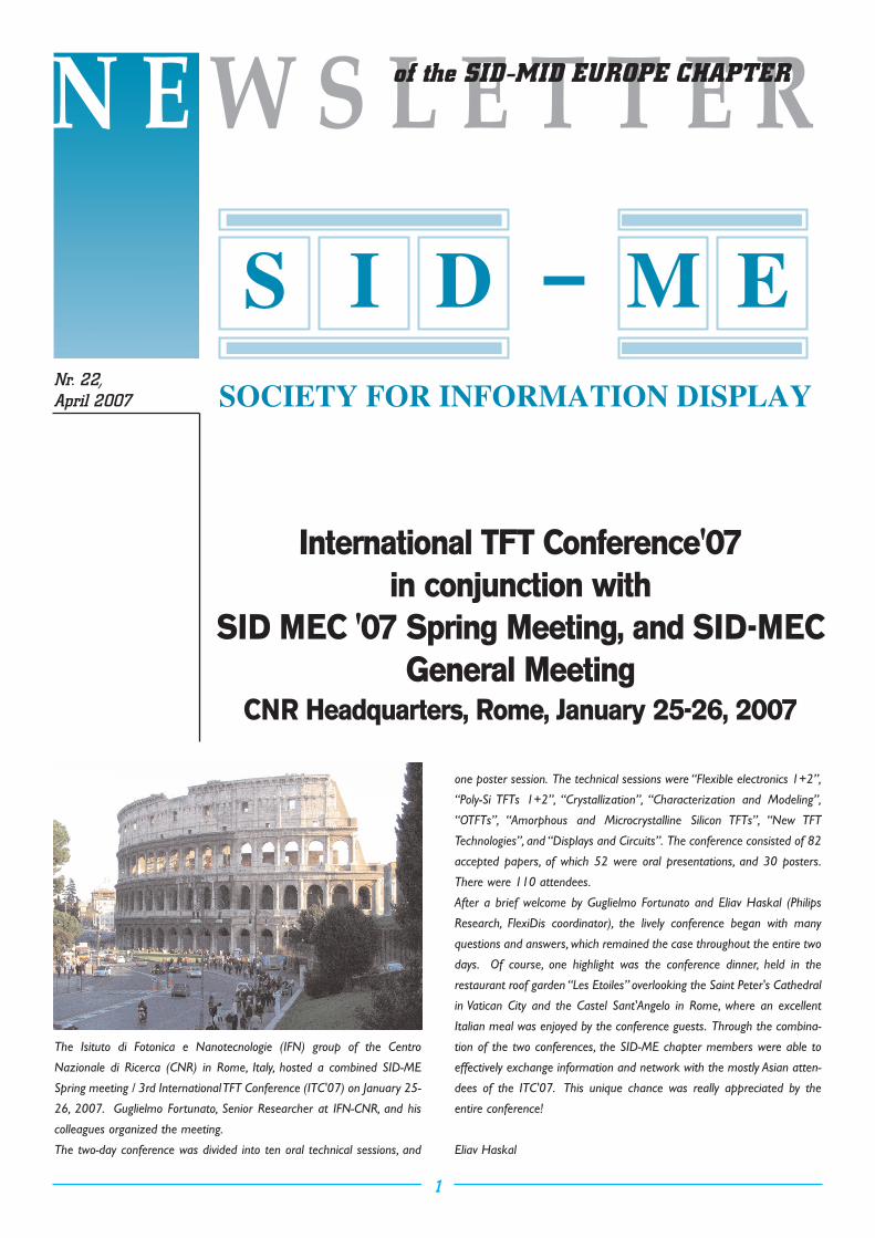
The Isituto di Fotonica e Nanotecnologie (IFN) group of the Centro
Nazionale di Ricerca (CNR) in Rome, Italy, hosted a combined SID-ME
Spring meeting / 3rd International TFT Conference (ITC'07) on January 25-
26, 2007. Guglielmo Fortunato, Senior Researcher at IFN-CNR, and his
colleagues organized the meeting.
The two-day conference was divided into ten oral technical sessions, and
one poster session. The technical sessions were “Flexible electronics 1+2”,
“Poly-Si TFTs 1+2”, “Crystallization”, “Characterization and Modeling”,
“OTFTs”, “Amorphous and Microcrystalline Silicon TFTs”, “New TFT
Technologies”, and “Displays and Circuits”. The conference consisted of 82
accepted papers, of which 52 were oral presentations, and 30 posters.
There were 110 attendees.
After a brief welcome by Guglielmo Fortunato and Eliav Haskal (Philips
Research, FlexiDis coordinator), the lively conference began with many
questions and answers, which remained the case throughout the entire two
days. Of course, one highlight was the conference dinner, held in the
restaurant roof garden “Les Etoiles” overlooking the Saint Peter's Cathedral
in Vatican City and the Castel Sant'Angelo in Rome, where an excellent
Italian meal was enjoyed by the conference guests. Through the combina-
tion of the two conferences, the SID-ME chapter members were able to
effectively exchange information and network with the mostly Asian atten-
dees of the ITC'07. This unique chance was really appreciated by the
entire conference!
Eliav Haskal
1
Nr. 22,April 2007
International TFT Conference'07in conjunction with
SID MEC '07 Spring Meeting, and SID-MECGeneral Meeting
CNR Headquarters, Rome, January 25-26, 2007
of the SID-MID EUROPE CHAPTER
Conference summary
This conference comprised 82 contributions with two sets of paral-
lel sessions. In view of this large number the usual SID-MEC
Newsletter summary, with a few lines devoted to each paper, where
an attempt is made to recall the main message or most important
result, is omitted. Instead, the programme with titles and authors is
included below.
ITC'07 / SID-MEC'07 Spring Meeting Conference programme
January 25
Session 1: Opening Session (9:00 - 9:15)
1.1: Welcome Address
G. Fortunato (CNR-IFN)
N. Fruehauf (Universität Stuttgart)
E. I. Haskal (Coordinator of FlexiDis Project - Philips Research, The
Netherlands)
Session 2: Flexible electronics (1)(9:15 - 10:35)(Session Chairman: E. Haskal)
2.1: 9:15-9:40 (Invited) Flexible active matrix electrophoretic
displays made with a standard a-Si:H TFT technology using
the EPLaRTM process
T. Kretz1, E. Chuiton1, G. Gomez1, F. Mazel1, I. French2, I. J. Boerefijn3
1 Thales Avionics LCD, MOIRANS, France
2 Philips Research Laboratory, Redhill, UK
3 Philips Applied Technologies, High Tech Campus 7, 5656AE Eindhoven,
The Netherlands
2.2: 9:40-10:05 (Invited) Flexible Thin-film Transistor for
Display Application
C.C. Lee,Yung-Hui Yeh, Jia-Chong Ho
Process Technology Division, Display Technology Center, Industrial
Technology Research Institute (ITRI)
2.3: 10:05-10:20 Printed organic transistors and plastic MEMS
switches for a large-area flexible wireless power transmis-
sion sheet
T. Someya1,T. Sekitani1, M.Takamiya2,Y. Noguchi1, S. Nakano1,T. Sakurai3.
1 Quantum-Phase Electronics Center, School of Engineering,The University
of Tokyo, Japan
2 VLSI Design and Education Center,The University of Tokyo, Japan
3 Center for Collaborative Research,The University of Tokyo, Japan
2.4: 10:20-10:35 Low-temperature polysilicon Thin Film
Transistors on Polyimide substrates for electronics on plastic
A. Pecora, L. Maiolo, M. Cuscunà, D. Simeone,A. Minotti, L. Mariucci and G.
Fortunato. Istituto di Fotonica e Nanotecnologie (IFN), CNR, Rome, Italy
10:35 - 10:50 Coffee Break
Session 3: Polysilicon TFTs (1)(10:50 - 12:25) (Session Chairman: P. Migliorato)
3.1: 10:50-11:15 (Invited) Single-Grain Si TFTs and Circuits
Fabricated through Advanced Excimer-Laser Crystallization
R. Ishihara,Vikas Rana, Ming He,Wim Metselaar and Kees Beenakker
Delft University of Technology,The Netherlands
3.2: 11:15-11:40 (Invited) Progress in Fabrication Processing of
Thin Film Transistors
K.Yoshioka and T. Sameshima
Tokyo University of Agriculture and Technology,Tokyo, Japan
3.3: 11:40-11:55 High-Performance Double-Gate LTPS Thin
Film Transistors Fabricated by Excimer Laser Irradiation
Chun-Chien Tsai1, Hsu-Hsin Chen1,Yao-Jen Lee2, Kai-Fang Wei1, Jyh-Liang
Wang1, Bo-Ting Chen1, and Huang-Chung Cheng1
1 Department of Electronics Engineering and Institute of Electronics,
National Chiao Tung University, Hsinchu,Taiwan
2 National Nano Device Laboratories, Hsinchu,Taiwan, ROC
3.4: 11:55-12:10 Fabrication of 3-Dimensionally Stacked Poly-
Si TFT CMOS Inverter with High Quality Laser Crystallized
Channel
Soon-Young Oh1, Chang-Geun Ahn1, Jong-Heon Yang1,Won-Ju Cho2,Woo-
Hyun-Lee2, Hyun-Mo Koo2, Seong-Jae Lee1
1 Nano-Bio Electronic Devices Team, Electronics and Telecommunications
Research Institute, Daejeon, KOREA
2 Eelectronic materials, Kwangwoon University, Seoul, KOREA
3.5: 12:10 - 12:25 High quality LTPS CMOS TFTs produced
with a five mask process and only one ion implantation step
P. Schalberger, H. Baur, S. Kohlenbecker, E. Persidis, and N. Fruehauf
Chair of Display Technology, Universität Stuttgart, Germany
12:25 - 13:45 Lunch
Session 4: Flexible electronics (2)(13:45 - 14:40) (Session Chairman:T. Noguchi)
4.1: 13:45 - 14:10 (Invited) Thin-film transistor backplanes on
flexible polymer and steel foil substrates
S.Wagner, A. Z. Kattamis, B. Hekmatshoar, K. H. Cherenack,
I-C. Cheng, H. Gleskova, J. C. Sturm. Department of Electrical Engineering,
Princeton University, New Jersey (USA)
4.2: 14:10 - 14:25 Near 100°C low temperature a-Si TFT array
fabrication on flexible PES and PEN substrates
Ivan V. Nikulin,Tae Hyung Hwang, Hyung Il Jeon, Sang Il Kim, Nam Seok
Roh, Seong Sik Shin
LCD R&D center, Samsung Electronics, Gyeonggi-Do, Korea
4.3: 14:25 - 14:40 Mechanical stability of poly-Si TFT on flexi-
ble metal foil
Jun Hyuk Cheon, Jung Ho Bae, and Jin Jang
Department of Information Display and Advanced Display Research
Center, Kyung Hee University, Seoul, Korea
14:40 - 14:55 Coffee Break
Session 5a: Crystallization(14:55 - 16:35)(Session Chairman: R. Ishihara)
5a.1: 14:55 - 15:20 (Invited) Location and Orientation Control
of Si Thin-Film Grains Using Metal Nano-Imprint Seeding of
2
Laser Annealing
T.Asano, and G. Nakagawa
Department of Electronics, Kyushu University, Fukuoka, JAPAN
5a.2: 15:20 - 15:35 2D-projection-based method for forming
uniform and high-quality poly-Si films via Sequential Lateral
Solidification
Brandon A.Turk1, Frank Simon2 and Rainer Pätzel2
1 Coherent, Inc., 5100 Patrick Henry Drive, Santa Clara, USA,
2 Coherent, GmbH, Göttingen, Germany
5a.3: 15:35 - 15:50 Growth of Si Crystalline in SiOx Films
Induced by Millisecond Rapid Thermal Annealing Using
Thermal Plasma Jet
Tatsuya Okada, Seiichiro Higashi, Hirotaka Kaku,Takuya Yorimoto, Hideki
Murakami and Seiichi Miyazaki
Department of Semiconductor Electronics and Integration Science
Graduate School of Advanced Sciences of Matter, Hiroshima University,
Japan
5a.4: 15:50 - 16:05 Growth Rate Measurement of Lateral
Grains in Silicon Film During Excimer Laser Annealing
Wenchang Yeh, Chunjun Zhuang, Dunyuan Ke
Department of Electronic Engineering, National Taiwan University of
Science and Technology, Taipei, Taiwan, Republic of Chinaanuary 25-26,
2007 - CNR Head
5a.5: 16:05 - 16:20 Enlargement of Grain size of Poly-Si using
Ferritin Protein with Ni Nanoparticles
Y. Nanjo,Y. Uraoka,T. Fuyuki, M. Okuda, I.Yamashita1
Nara Institute of Science and Technology, Nara, Japan
1 ATRL, Matsushita Electric Industrial Co., Ltd., Seika, Kyoto (Japan)
5a.6: 16:20 - 16:35 Hydrogen Effect in Excimer Laser
Annealing of Hydrogen Modulation Doped a-Si Film
A. Heya, K. Oda,T. Serikawa*, N. Kawamoto** and N. Matsuo
University of Hyogo, Japan
*Osaka University, Japan
**Yamaguchi University, Japan
Session 5b: Characterization and modeling(14:55 - 16:40)(Session Chairman:Y. Uraoka)
5b.1 14:55 - 15:10 Hot carrier stress induced degradation of
SLS ELA polysilicon TFTs - Effects of gate width variation
and device orientation
G. P. Kontogiannopoulos1, F.V. Farmakis1,D.N. Kouvatsos1, G. J. Papaioannou2
and A.T.Voutsas3
1 Institute of Microelectronics, NCSR Demokritos, Agia Paraskevi 15310,
Greece
2 Physics Department, University of Athens, Athens 157 84, Greece
3 LCD Process Technology Laboratory, Sharp Labs of America, Camas,WA,
USA
5b.2: 15:10 - 15:25 Reliability for Joule effect in LTPS-TFTs
with very thin gate oxide
H. Ueno,Y. Sugawara,Y. Uraoka and T. Fuyuki,T. Serikawa*
Graduate School of Materials Science, Nara Institute of Science and
Technology , Japan
* Joining and Welding Research Institute, Osaka University
5b.3: 15:25 - 15:40 Degradation Mechanisms of NBTI and
PBTI in Low-Temperature Poly-Si Thin-Film Transistors
C.-Y. Chen1, J.-W. Lee2,W.-C. Chen3, H.-Y. Lin3, K.-L.Yeh3, S.-D.Wang1,
T.-F. Lei1
1 Institute of Electronics, National Chiao Tung University,Taiwan, R. O. C.
2 National Nano Device Laboratory, Hsin-Chu,Taiwan, R.O.C.
3 Toppoly Optoelectronics Corp., Miao-Li,Taiwan, R. O. C.
5b.4: 15:40 - 15:55 Effective Dopant Activation of Si film using
ELA for Advanced Si TFT
Takashi NOGUCHI
Dept. of Electrical and Electronics Engineering, University of the Ryukyus,
1 Senbaru, Nishihara, Okinawa-ken, Japan
5b.5: 15:55 - 16:10 Investigation of the undershoot effect in
polycrystalline silicon thin film transistors
L. Michalas1, G.J. Papaioannou1, D.N. Kouvatsos2, A.T.Voutsas3
1 Physics Department, National and Kapodistrian University of Athens,
Greece
2 Institute of Microelectronics, NCSR "Demokritos",Aghia Paraskevi Attikis,
Athens, Greece
3 LCD Process Technology Laboratory, Sharp Labs of America, Camas,WA,
USA
5b.6: 16:10 - 16:25 Universal compact model for long- and
short-channel Thin-Film Transistors
B. Iñiguez1, R. Picos2, D.Veksler3,A. Koudymov3, and M. S. Shur3,T.Ytterdal4,
W. Jackson5
1 DEEEA, Universitat Rovira i Virgili, Avda. Països Catalans 26,Tarragona,
Spain
2 Physics Department, Universitat de les Illes Balears, Palma de Mallorca.
Spain
3 ECSE and Broadband Center, Rensselaer Polytechnic Institute,Troy, NY,
USA
4 Department of Physical Electronics" to "Department of Electronics and
Telecommunication, Norwegian University of Science and Technology,
Trondheim, Norway
5 HP Labs, Palo Alto, CA, USA
5b.7: 16:25 - 16:40 Analytical Model of Current-Voltage
Characteristics in On-state Poly-Si TFT"
Tadsahi Serikawa
Osaka University
SID-Mid Europe Chapter Meeting(Members only) (17:00)
Poster session (16:40 - 18:10)
P1: Novel Surface Treatment of Plastic Substrate using
Atomic Hydrogen for Flexible Displays
Akira Heya, Masahiko Sato and Naoto Matsuo
University of Hyogo, Japan
P2: High-Performance Self-Aligned Bottom-Gate LTPS
TFTs Fabricated by Excimer Laser Irradiation with
3
P2: High-Performance Self-Aligned Bottom-Gate LTPS
TFTs Fabricated by Excimer Laser Irradiation with
Backside Exposure Photolithography
C.C.Tsai, H.-H. Chen,Y.J. Lee1, K.F.Wei, J.L.Wang, B.T. Chen, H.C. Cheng
Department of Electronics Engineering and Institute of Electronics,
National Chiao Tung University, Hsinchu,Taiwan
1 National Nano Device Laboratories, Hsinchu,Taiwan, ROC
P3: Improvement in Si/SiO2 properties using atmospheric
pressure plasma
T. Miyamoto,Y. Sugawara,Y. Uraoka,T. Fuyuki, H. Kuroda1, K.Takashima1
Nara Institute of Science and Technology, Nara 630-0192, Japan
1 e Square Co.,Ltd., Kyoto, Japan
P4: Hafniun oxide deosited at room temperature by reac-
tive RF magnetron sputtering from a metallic target for
thin film transistors
Y. J. Choi1, C. Ducati2,Y. Fu1, S. P. Speakman3 and A. J. Flewitt1
1 Electrical Engineering Division, Cambridge University, Cambridge, U.K
2 Department of Materials Science and Metallurgy, Cambridge University,
Pembroke Street, Cambridge,U.K
3 3T Technologies Ltd., 7, Essex, U.K
P5: Fabricated Si Nanowire using Nanoimprint Method
Jin-Woo HAN, Dong-Hun KANG, Chul-Ho OK, Dae-Shik SEO.
Department of Electrical and Electronic Engineering College of
Engineering,Yonsei University, Seoul, Korea
P6: Low Temperature Formation of Si Oxide Thin Film for
TFT by Reaction of Organosilicon polymer and Low
Concentration Ozone Gas
Kensuke NISHIOKA, Kouichi TORIYABE and Susumu HORITA
Graduate School of Materials Science, Japan Advanced Institute of Science
and Technology, Ishikawa, Japan
P7: CMOS LTPS-TFTs by using CW laser crystallization
Yong Duck Son, Kyung Dong Yang, Nam Kil Son, Eun-Hyun Kim, and
Jin Jang
Department of Information Display and Advanced Display Research
Center, Kyung Hee University, Korea
P8: High-Performance Poly-Si TFTs Fabricated by Floating
Channel Crystallization Technology
Chia-Wen Chang, Jam-Wem Lee1, Che-Lun Chang, and Tan-Fu Lei
Department of Electronics Engineering and Institute of Electronics,
National Chiao-Tung University, Hsin-Chu,Taiwan, R.O.C.
1 National Nano Device Laboratory, Hsin-Chu,Taiwan, R.O.C.
P9: Plane-to-Line Switching (PLS) Mode-Based Thin Film
Transistor-Liquid Crystal Display (TFT-LCD) Adopting a
Novel Concept of Process Architecture
Jae-Bok LEE, Chun-Ki YOU, Seong-Jun LEE, Hoon-Kee MIN and, Chi-Woo
KIM
Mobile Display Process Development Team, LCD Business, Samsung
Electronics Co., Ltd.San #24, Nongseo-dong, Kiheung-Ku, Yongin-City,
Gyeonggi-Do, KOREA
P10: External Compensation of LTPS AMOLED Displays
based on a Three TFTs Pixel Circuit
F. Pieralisi1, H. Baur1, E. Persidis1 and N. FRuehauf1,T. Marx2,
H. Schemmann2, S.Weitbruch2 , P. Le Roy3
1 Chair of Display Technology, Universität Stuttgart, 70569 Stuttgart,
Germany
2 THOMSON Deutsche Thomson Brandt GmbH
3 THOMSON R&D France
P11: Leakage current-Free Pixel Structure Using a Shield
Capacitor for Active-Matrix Display
Hyun-Sang Park, Jae-Hoon Lee and Min-Koo Han
School of Electrical Engineering (#50), Seoul National University, Seoul,
Korea
P12: A New Amorphous Silicon Gate Driver with Stable
Operation
J.W. Choi, J.H. Koo,Y.S. Kim, M.H..Kang, E.B.Kim, S.H. Kim, S.-W. Lee, J. Jang
Department of Information Display and Advanced Display Research
Center, Kyung Hee University, Seoul, Korea
P13:Two dimensional numerical simulation of low frequen-
cy noise in polysilicon thin film transistors
A. Boukhenoufa, C. Cordier, L. Pichon1, B. Cretu
Groupe de Recherches en Informatique, Image, Automatique et
Instrumentation de Caen (GREYC), CNRS UMR, ENSICAEN-Université de
Caen, France
1Groupe Microélectronique, IETR, UMR CNRS Rennes, France
P14: Electrical instability in self-aligned p-channel polysili-
con TFTs related to oxide residual damage
M. Rapisarda1, L. Mariucci1, A.Valletta1, A. Pecora1 and G. Fortunato1,
C.Caligiore2, E. Fontana2, S. Leonardi2, F.Tramontana2
1 CNR-IFN, Roma, Italy
2 STMicroelectronics, Catania, Italy
P15: Hot carrier effects in p-channel polysilicon thin film
transistors
P. Gaucci1, L. Mariucci1, A. Valletta1, M. Cuscunà1, L. Maiolo1, A. Pecora1,
G.Fortunato1, F.Templier2
1 CNR-IFN, Roma, Italy
2 CEA-LETI, Département IHS, 17 rue des Martyrs, Grenoble, France.
P16: Effects of bias stress on low temperature polysilicon
TFTs
D. Palumbo1, S. Masala1, P.Tassini1, A. Rubino2, D. Della Sala3
1 ENEA C. R. Portici, Portici (NA), Italy
2 DIIE, University of Salerno, Fisciano (SA), Italy
3 ENEA C. R. Casaccia, S. Maria di Galeria (Roma), Italy
P17: A New Poly-Si Thin-Film Transistor Nonvolatile Ge
Nanocrystals Memory with High Programming / Erasing
Efficiency
Po-Yi Kuo1,Tien-Sheng Chao2, Jyun-Siang Huang2, and Tan-Fu Lei1
1 Department of Electronics Engineering and Institute of Electronics,
National Chiao-Tung University, Hsin-chu,Taiwan, R.O.C.
2 Department of Electrophysics, National Chiao-Tung University, Hsinchu,
Taiwan, R.O.C.
P18: Characterization of advanced directional SLS ELA
polysilicon TFTs -Dependence of device parameters on ori-
entation and geometry-
D. C. Moschou1, D. N. Kouvatsos1, F.V. Farmakis1, A.T.Voutsas2
4

transient behavior of advanced excimer laser crystallized
polysilicon thin film transistors
Michael A. Exarchos1, L.Michalas1, G.J.Papaioannou1, D.N.Kouvatsos2,
A.T.Voutsas3
1 National and Kapodistrian University of Athens (NKUA), Physics
Department, Solid State Physics Section, Athens, Greece
2 National Center of Scientific Research (NCSR) "DEMOKRITOS", Institute
of Microelectronics, Greece
3 SHARP Labs of America, LCD Process Technology Laboratory,Washington,
USA
P20: DC Modeling of Single-Grain Si TFTs using BSIMSOI
Alessandro Baiano, Ryoichi Ishihara, Nobuo Karaki1 and Satoshi Inoue1,
Wim Metselaar and Kees Beenakker
Delft University of Technology, Feldmannweg 14, 2628 CT Delft,
The Netherlands
1 Seiko Epson Cooperation, Nagano 399-0293, Japan
P21: Comparison of Defect Densities in Excimer Laser and
Thermal Plasma Jet Crystallized Si Films
S. Higashi,T.Yorimoto,T. Okada, H. Kaku, H. Murakami and S. Miyazaki
Graduate School of Advanced Sciences of Matter, Hiroshima University,
Japan
P22: _-PCD Measurement of Double-Layered poly-Si Thin
Films Crystallized by Solid Green Laser Annealing
Y. Sugawara1,Y. Uraoka1, H.Yano1,T. Hatayama1 and T. Fuyuki1,A. Mimura2
1 Nara Institute of Science and Technology, Nara, Japan
2 National Institute of Advanced Industrial Science and Technology, Ibaraki,
Japan
P23: OTFT Circuits on Plastic Manufactured by Self-
Organized Process
S. H. Han, S. H. Lee,Y. R. Son, K. J. Lee, G. S. Cho,W. S. Kim, D. J. Choo2 and
J.Jang
Department of Information Display and Advanced Display Research
Center Kyung Hee University, Hoegi-dong 1, Seoul, Korea
P24: Soluble Anthracene Oligomers Containing Thiophene
Derivatives for Organic Thin Film Transistors
Jong-Hwa Park,Young Kwan Jung,Taek Ahn1, Mi Hye Yi1, Hong-Ku Shim
Department of Chemistry and School of Molecular Science, Korea
Advanced Institute of Science and Technology, Yuseong-Gu, Daejeon,
Republic of Korea
1Polymeric Nanomaterials Laboratory, Korea Research Institute of
Chemical Technology,Yuseong-gu, Daejeon , Republic of Korea
P25: Study for characteristics of spin on dihexylsexithio-
phene thin film transistor
Jae-Hong Kwon1, Jung-Hoon Seo1, Dong Hoon Choi2, Yun-Hi Lee3, and
Byeong-Kwon Ju1
1 Display and Nanosystem lab., School of Electrical Engineering, College of
Engineering, Korea University, Korea
2 Functional Polymer Chemistry Lab., College of Science, Korea University,
Anam-Dong, Seongbuk-Gu, Seoul, Korea
3 National Research Laboratory, Nano Device & Physics Lab., Department
of Physics, Korea University, Korea
P26: Post-Treatment Effects on the Electrical Characteris-
tics of Ink-jet Printed Triisopropylsilyl Pentacene Organic
Thin-Film Transistors
Y.-H. Kim1,2, S.-M. Han2, J.-H. Lee2, J.-I. Han1 and M.-K. Han2
1 Information Display Research Center, Korea Electronics Technology
Institute, Kyunggi, Korea
2 School of Electric Engineering and Computer Science, Seoul National
University, Seoul, Korea
P27: Insulator Passivation of Organic Thin-Film Transistor
for Improving Device Performance
J.H. Seo, J.H. Kwon, K.S. Seo1 and B.K. Ju2
1 Convergence & Components Laboratory (ICCL), Electronics and
Telecommunications Research Institute (ETRI), Daejeon, 305-700, KOREA
2 Display and Nanosystem Laboratory, School of Electrical Engineering,
Korea University, Seoul 136-701, Korea
P28: Improvement of threshold voltage stability with bot-
tom-gate polymorphous silicon Thin Film Transistors
François TEMPLIER1, Maher OUDWAN1, Frederic SERMET1, Alexey
ABRAMOV2,3 and Pere ROCA i CABARROCAS2
1 CEA-LETI, DIHS,Grenoble, France
2 LPICM, Ecole Polytechnique, CNRS, Palaiseau, France
3 A.F.Ioffe Phys.-Technical Institute, St.-Petersburg, Russia
P29:P-type Microcrystalline Silicon for Thin Film Transistors
Y. Djeridane,V.D. Bui, A. Abramov,Y. Bonnasieux, P. Roca i Cabarrocas
LPICM CNRS Ecole polytechnique Palaiseau, France
P30: Reduction of off current in ITO-channel thin film tran-
sistor with ferroelectric (Bi,La)4Ti3O12 gate insulator
Eisuke Tokumitsu,Tomofumi Fujimura,Takashi Sato, Etsu Shin and
Masaru Senoo
Precision and Intelligence Laboratory, Tokyo Institute of Technology,
Yokohama, Japan
19:30 Banquet
January 26
Session 6a: O-TFTs(8:30 - 10:30)(Session Chairman: N. Fruehauf)
6a.1: 8:30 - 8:55 (Invited) Optimisation of Organic Semicon-
ductors for Flexible Display Backplanes
M. Coelle
Merck
6a.2: 8:55 - 9:20 (Invited) Organic Thin Film Transistors for
Flexible Display Applications
S. Burns
Plastic Logic Limited, Cambridge, United Kingdom
6a.3: 9:20 - 9:45 (Invited) Selective Growth of Large-Grain
Organic Semiconductor by Self-Organized Process
J.Jang and Seung Hoon Han
Dept. of Information Display, Kyung Hee University, Korea
6a.4: 9:45 - 10:00 Effect of active layer thickness on electrical
characteristics of pentacene TFTs with PMMA buffer layer
L. Mariucci1, D. Simeone1, S. Cipolloni1, L. Maiolo1, A. Pecora1 and G.
Fortunato1, S. Brotherton2
5
1 CNR-IFN, Roma, Italy
2 TFT Consultant, 12 Riverside, Forest Row, UK
6a.5: 10:00 - 10:15 Electrode configuration for n-type organic
transistors with top-contact type fabricated by solution
process
Yutaka Ohmori, Dr. Hirotake Kajii, and Syohei Fukuda
Osaka University, Center for Advanced Science and Innovation, Japan
6a.6: 10:15 - 10:30 OFET for gas sensing based on pentacene
films grown by SuMBE
T.Toccoli, A. Pallaoro, M.Tonezzer, N. Coppedè and S. Iannotta
IFN-CNR _Trento Division - Italy
Session 6b: Amorphous and microcrys-talline silicon TFTs(8:30 - 9:55)(Session Chairman: M.K. Han)
6b.1: 8:30 - 8:55 (Invited) Critical Issues in Plasma Deposition
of Microcrystalline Silicon for Thin Film Transistors
P. Roca y Cabarrocas1,Yassine Djeridane1 and Alexey Abramov12
1 LPICM, Ecole Polytechnique, CNRS, Palaiseau, France
2 A.F.Ioffe Phys.-Technical Institute, St.-Petersburg, Russia
6b.2: 8:55 - 9:10 New structure of a-Si:H TFT for controlling
backlight brightness
Se Hwan Kim1, Eung Bum Kim1, Hee Yeon Choi1, Dong Han Kang1,Won
Hoon Park1, Jae Hwan Oh1, Moon Hyo Kang1, Ji Ho Hur1, Jung Woo
Lee2, Jung Ryoul Choi2, Seung Hun Ahn2, Soon Won Hong2and Jin Jang1
1 Advanced Display Research Center Kyung Hee University, Seoul,
Korea
2 Technology Leaders & Innovators, Kyunggi-Do, Korea
6b.3: 9:10 - 9:25 All Hot Wire CVD TFTs with High
Deposition Rate Silicon Nitride (3 nm/s)
R.E.I. Schropp, S. Nishizaki1, Z.S. Houweling,V.Verlaan, C.H.M van der Werf
, H.Matsumura1
Utrecht University, Faculty of Science, Department of Physics and
Astronomy, SID -Physics of Devices, Utrecht, the Netherlands
1Japan Advanced Institute of Science and Technology (JAIST), Ishikawa,
Japan
6b.4: 9:25 - 9:40 Influence of the deposition temperature on
the performance of microcrystalline silicon thin film tran-
sistors
M. Oudwan,A. Abramov1, P. Roca i Cabarrocas1 and F.Templier
CEA-LETI, DIHS, Grenoble, France
1 LPICM, Ecole Polytechnique, CNRS, Palaiseau, France
6b.5 : 9:40 - 9:55 Microcrystalline TFTs:VerilogA Modeling
O. Moustapha,V.D. BUI,Y .Bonnasieux, J.Y. Parey
Laboratoire de Physique des Interfaces et Couches Minces LPICM-Ecole
Polytechnique, France
10:30 - 10:45 Coffee Break
Session 7: New TFT technologies(10:45 - 12:45)(Session Chairman: J. Jang)
7.1: 10:45 - 11:10 (Invited)
Is the future of TFTs transparent?
Elvira Fortunato1 Pedro Barquinha1 Luís Pereira1 Gonçalo Gonçalves1 and
Rodrigo Martins2
1 Department of Materials Science/CENIMAT, Faculty of Sciences and
Technology, New University of Lisbon, Campus da Caparica, 2829-516
Caparica, Portugal
2 CEMOP-UNINOVA, Campus da Caparica, 2829-516 Caparica, Portugal
7.2: 11:10 - 11:25 Amorphous In-Zn-Ga-O based TFTs and
circuits
R. Hayashi, M. Ofuji, N. Kaji, K. Abe, H.Yabuta, M. Sano, and H. Kumomi
K. Nomura*,T. Kamiya*, M. Hirano*, and H. Hosono*
Canon Research Center,Tokyo, Japan
*Tokyo Institute of Technology,Yokohama, Japan
7.3: 11:25 - 11:40
Ink-jet printed carbon nanotube thin film transistors
P. Beecher1, P. Servati1, A. Rozhin1, A. Colli1,V. Scardaci1, S. Pisana1,
G.W. Hsieh1, A. Fasoli1, D. Chu1, F. M. Li2, A. Nathan3, B. Ong4,A. Flewitt1, J.
Robertson1, A. Ferrari1 and W. I. Milne1
1 Department of Engineering, University of Cambridge, Cambridge, CB3
0FA, UK
2 Electrical and Computer Engineering, University of Waterloo,Waterloo,
Ontario, N2L 3G1, Canada
3 London Centre for Nanotechnology, University College London, London,
WC1H0AH, UK
4 Xerox Research Centre of Canada, Mississauga, Ontario, L5K 2L1,
Canada
7.4: 11:40 - 11:55
Solution-deposited carbon nanotube network TFTs on glass
and flexible substrates
A. Schindler*,A. Lindner*, S. Goettling*, N. Fruehauf*, J. P. Novak**,
Z.Yaniv**
* Chair of Display Technology, Universitaet Stuttgart, Germany
** Applied Nanotech Inc., USA
7.5: 11:55 - 12:10 Probing the electronic characteristics of sin-
gle bionanodot
R.Tanaka,A. Miura,Y. Uraoka,T. Fuyuki, I.Yamashita*
Graduate school of Materials Science, Nara Institute of Science and
Technology, Nara, Japan
*Advanced Technology Research Labs., Matsushita Electric Industrial, Japan
7.6: 12:10 - 12:25 Low-Temperature Solid-Phase
Crystallization of Amorphous SiGe Films on Glass by
Imprint Technique
K.TOKO, H. KANNO,A. KENJO,T. SADOH,T.ASANO and M. MIYAO
Department of Electronics, Kyushu University, Fukuoka, JAPAN
7.7: :12:25 - 12:50 (Invited) Source-Gated Thin-Film Transistors
J. M. Shannon and F. Balon
Advanced Technology Institute, University of Surrey, United Kingdom
12:50 - 14:00 Lunch
6
Sessin 8: Displays and circuits(14:00 - 15:10) (Session Chairman: F.Templier)
8.1: 14:00 - 14:25 (Invited) Novel Mobile TFT-LCDs Based on
SLS Technology
C.W. Kim, J.B. Choi, K.C. Moon, J.H. Eom, R.Yokoyama, K.C. Park
Mobile Display Business Team, LCD Business, Samsung Electronics Co., LTD
8.2: 14:25 - 14:40
LTPS-TFT process for AMOLED-displays
E. Persidis, H. Baur, R. Hlawatsch, F. Pieralisi, P. Sschalberger, N. Fruehauf
Chair of Display Technology, Universität Stuttgart, Germany
8.3: 14:40 - 14:55
A new LTPS-TFT pixel for AMOLED to suppress the hys-
teresis effect on OLED current by employing a reset voltage
driving
Jae-Hoon Lee, Sang-Myeon Han, Sang-Geun Park, Yong-Hoon KIM and
Min-Koo HAN
School of Electrical Engineering #50, Seoul National University, Seoul,
Korea
8.4: 14:55 - 15:10 Suppression of TFT leakage current effect
on active matrix displays by employing a new circular
Switch
Jae-Hoon Lee, Hyun-Sang Park, Sang-Myeon Han, and Min-Koo Han
School of Electrical Engineering Seoul National University, Seoul, Korea
15:10 - 15:25 Coffee Break
Session 9: Polysilicon TFTs (2)(15:25 - 16:40)(Session Chairman: G. Fortunato)
9.1: 15:25 - 15:40
Grain Boundary characterisation in Sequentially Laterally
Solidified Polycrystalline-Silicon Thin Film Transistors
A Valletta,A Bonfiglietti, M Rapisarda, L Mariucci,A Pecora, G Fortunato, and
S D Brotherton*
IFN-CNR,Via Cineto Romano 42, Roma 00156, Italy
* TFT Consultant, 12 Riverside, Forest Row, RH18 5HB, UK
9.2: 15:40 - 15:55
Low temperature poly-Si TFT Flash memory with Si nano
crystal dot
K. Ichikawa, H.Yano,T. Hatayama,Y. Uraoka,T. Fuyuki, A.Tomyo*,
E.Takahashi*,T. Hayashi*, K. Ogata*
Nara Institute of Science and TechnologyNara, Japan
*1 NISSIN ELECTRIC CO.,LTD. Kyoto, Japan
9.3: 15:55 - 16:10 Low-cost poly-Si TFT with non-laser crys-
tallization of amorphous silicon
J. H. Oh, D. H. Kang,W. H. Park, K.W.Ahn, S.H. Park, J. H. Hur, J. Jang,
Y.-J.Chang*, J.-B. Choi*, H.-K. Min*, C.-W. Kim*
Advanced Display Research Center and Department of Information dis-
play, Kyung Hee University, Seoul, Korea
* Mobile Display Business Team, LCD Business, Samsung Electronics,
Gyeonggi-Do, Korea
9.4: 16:10 - 16:25 High Electrical Performance LTPS P-Type
and N-Type Polycrystalline Silicon Thin-Film Transistors
C. Caligiore, E. Fontana, S. Leonardi, F.Tramontana
STMicroelectronics, Catania (Italy)
9.5: 16:25 - 16:40 Improvement on Performance and Reli-
ability of TaN/HfO2 LTPS-TFTs with Fluorine Implantation
Ming-Wen Ma, Tsung-Yu Yang*, Kuo-Hsing Kao*, Tien-Sheng Chao*, and
Tan-Fu Lei
Institute of Electronics, National Chiao Tung University,Taiwan, R.O.C
* Inst. and Dept. of Electrophysics, National Chiao Tung University, Hsinchu,
Taiwan
SID-MEC General Meeting
Eliav Haskal (Philips Research) chaired the SID-MEC general meeting,
where the status of the chapter was reported, and the election of the
officers of the SID-ME chapter for the coming period took place.
Gerrit Oversluizen was abdicating as vice- chair. Armin Wedel
(Fraunhofer IAP) was the nominated new vice-chair.The other offi-
cers volunteered to run for another term, and the proposed candi-
dates were elected unanimously.The new Chapter committee is now
composed as follows: Patrick Vandenberghe (Chair), Armin Wedel
(Vice-Chair), Herbert De Smet (Secretary), Jutta Rasp (Treasurer).
SID-MEC membership: with 555 members in January 2007, the SID-
ME chapter has lost 10% compared to January 2006.This is primari-
ly due to the expiration of the Eurodisplay'05 memberships. Overall,
the membership is fairly constant over a period of 3 years. SID-ME
has 8.2% of all 6747 SID members and is now the third largest chap-
ter, after Japan (1130) and Bay Area (585) and before Korea (525).
The110 participants of this joint SID-MEC'07 spring meeting/ITC'07
meeting show that SID-MEC meetings continue to attract a high
attendance.
Jutta Rasp could unfortunately not attend the meeting; hence the pre-
sentation of the financial status is postponed until the next general
meeting.
This years student award was cancelled;see below.
Also the upcoming meetings were announced. There will be no
Fall'07 SID-MEC meeting; but there will be an officers' meeting dur-
ing the Eurodisplay'07 Conference (17-20 September 2007,
Moscow). The SID-MEC Spring'08 meeting will be held from 13-14
March 2008 in Jena at the Fraunhofer IOF.
Conference dinnerThe SID-MEC/ITC'07 conference dinner event took place on the
25th evening at the Restaurant Roof Garden “Les Etoiles”. This
restaurant offers a beautiful panorama over Rome with views of St
Peter's.
The view from this roof-garden restaurant near the Vatican was mag-
nificent, and the menu was excellent.The restaurant was decorated
with wonderful wall tapestry, elegant furniture and exclusive interior.
7
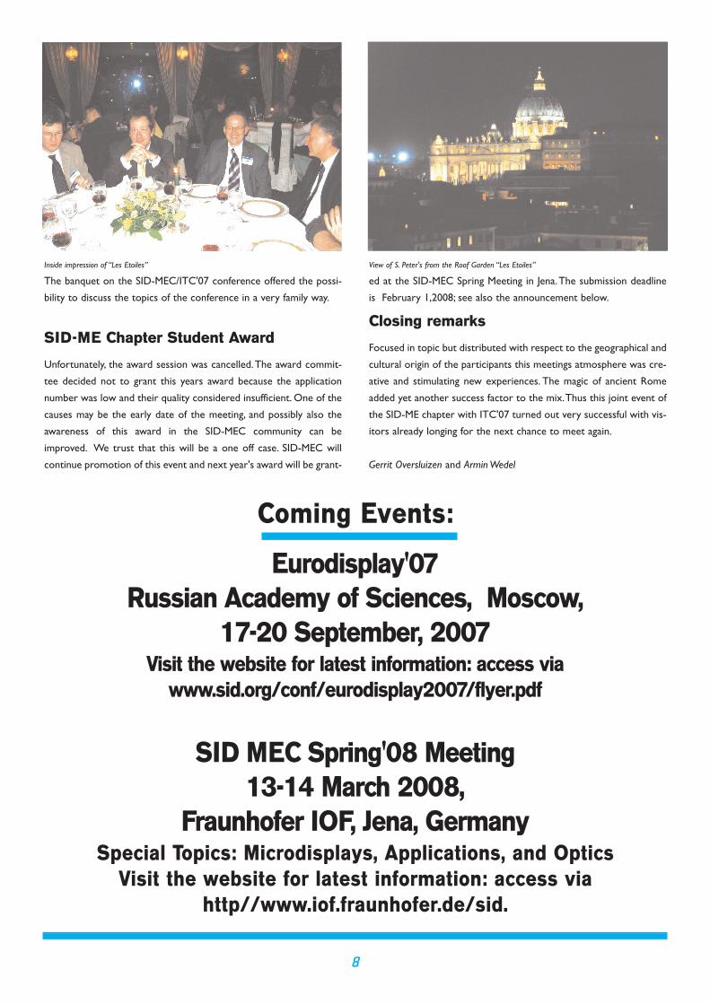
Inside impression of “Les Etoiles”
The banquet on the SID-MEC/ITC'07 conference offered the possi-
bility to discuss the topics of the conference in a very family way.
SID-ME Chapter Student Award
Unfortunately, the award session was cancelled.The award commit-
tee decided not to grant this years award because the application
number was low and their quality considered insufficient. One of the
causes may be the early date of the meeting, and possibly also the
awareness of this award in the SID-MEC community can be
improved. We trust that this will be a one off case. SID-MEC will
continue promotion of this event and next year's award will be grant-
View of S. Peter's from the Roof Garden “Les Etoiles”
ed at the SID-MEC Spring Meeting in Jena.The submission deadline
is February 1,2008; see also the announcement below.
Closing remarks
Focused in topic but distributed with respect to the geographical and
cultural origin of the participants this meetings atmosphere was cre-
ative and stimulating new experiences. The magic of ancient Rome
added yet another success factor to the mix.Thus this joint event of
the SID-ME chapter with ITC'07 turned out very successful with vis-
itors already longing for the next chance to meet again.
Gerrit Oversluizen and Armin Wedel
8
Eurodisplay'07Russian Academy of Sciences, Moscow,
17-20 September, 2007Visit the website for latest information: access via
www.sid.org/conf/eurodisplay2007/flyer.pdf
SID MEC Spring'08 Meeting13-14 March 2008,
Fraunhofer IOF, Jena, GermanySpecial Topics: Microdisplays, Applications, and Optics
Visit the website for latest information: access viahttp//www.iof.fraunhofer.de/sid.
Coming Events:
9
SID-ME Chapter committee
The SID-ME Chapter committee is now formed by:
Ing. P.Vandenberghe (chair), Barco, Pres. Kennedypark 35,
B8500 Kortrijk, Belgium.
Tel.: +32 56 233216, Fax: +32 56 232279
E-mail: [email protected]
Dr. A. Wedel (vice-chair), Fraunhofer Institute for Applied Polymer
Research, Geiselbergstrasse 69, Potsdam, Germany,
Tel.: +49 3315681910, Fax: +49 331 5683910,
E-mail: [email protected]
Prof.Dr. H. De Smet (secretary), Ghent University,Technologiepark
914 A, B-9052 Zwijnaarde, Belgium,
Tel.: +32 9 264 5363, Fax: +32 9 264 5374,
E-mail: [email protected]
J. Rasp (treasurer), Flat Panel Displays,Alpenstrasse 12, Postfach 1208,
D-85619 Feldkirchen, Germany.
Tel.: +49 8990955494, Fax: +49 8990955495
E-mail: [email protected]
Additional members of the SID MEChapter committee are:Dr.-Ing.N.Frühauf (directordirector SID-ME chapter), Universität
Stuttgart,Allmandring 3B, D-70550 Stuttgart-Vaihingen, Germany,
Tel.: +49 711 685 66922,
Fax: +49 711 685 66924.
E-mail: [email protected]
Lic.Tech. J.Kimmel, Nokia Research Center, P.O. Box 100,
FIN-33721 Tampere, Finland,
Tel.: +358 7180 35484, Mobile: +358 50 48 35484,
Fax: +358 7180 35322, E-mail: [email protected]
Dr.G. Oversluizen, Philips Research, Prof. Holstlaan 4, 5656 AA, Eindhoven,
The Netherlands,Tel.: +31 40 2747715, Fax: +31 40 2746321,
E-mail: [email protected]
Dr.Michael E. Becker, Display-Metrology & Systems,
Marie-Alexandra Str. 44, D 76135 Karlsruhe-Germany,
Tel./Fax: +49 721 981 2268
E-mail: [email protected]
Dr.W.Becker, Merck KGaA
Frankfurter Str. 250, D-64293 Darmstadt, Germany,
Tel.: +49 6151 72 7360 ; Fax: +49 6151 72 3132
E-mail: [email protected]
Prof.Dr. P. Maltese, University La Sapienza,Via Marmorata 169, I-00153
Roma, Italy,
Tel.: +39 644 585 428, Fax: +39 647 42 647.
Dr. M. Schadt, Rolic Research Ltd, Gewerbestrasse 18,
CH-4123 Allschwil, Switzerland,
Tel.: +41 61 487 22 22, Fax: +41 61 487 22 88
E-mail: [email protected]
Dr. D.Theis, Siemens AG,
Tel.: +49 89 636 40550, Fax.: +49 89 636 40554,
E-mail: [email protected]
Dipl.Ing. F. Rochow, LMT Lichtmesstechnik GmbH, Helmholtzstrasse
9, D-10587 Berlin, Germany,
Tel.: +49 30 393 40 28, Fax: +49 30 391 80 01,
E-mail: [email protected]
Prof.Dr. A. van Calster, Ghent University,Technologiepark 914 A, B-9052
Zwijnaarde, Belgium,
Tel.: +32 9 2645364, Fax: +32 9 264 5374,
E-mail: [email protected]
SID payment.The SID annual membership fee amounts US$ 75. Please note that
the membership is now a rolling membership, which means that it
runs 12 months from the month in which the payment was made.
For more information see the SID website www.sid.org.
We encourage our members to pay directly to SID-HQ in the
USA, but if they want to pay to the ME-Chapter directly the annu-
al fee should be EUR 70 with all bank fees covered by the
member !
Please note that due to the change in the US dollar/Euro exchange
rate SID-MEC has re-evaluated the membership fee. In case of direct
payment to the SID-ME Chapter the payment in EURO should be
done to
Account no.: 206 020 1104
at: Berliner Sparkasse, Berlin,Germany
Bank code: BLZ 100 500 00
Account name: Frank Rochow, SID-ME
Please indicate your name on the remittance papers.
The Newsletter.If you want to place an article in the Newsletter, which is interesting
for the European display society, please send it to:
G. Oversluizen, fax: +31 40 274 6321,
E-mail: [email protected]
10
SID-ME Chapter Student Award
Call for SID-ME Chapter Student Award
The SID-ME Chapter Student Award is given for an outstanding scientific or technical achievement in, or contribution to, research on informa-
tion display.The applicant is a student at a university/institute in the SID-ME region.The award amounts to 1500 Euro, with the obligation to
present the contribution at the SID-MEC meeting where the award is presented.The conference fee is waived. The applicant must be a mem-
ber of SID. For information on student membership, see below.The application deadline for the Spring'08 meeting in Jena is February 1, 2008
Application for SID-ME Chapter Student Award
Name: _________________________________________________________________________________________________
SID Membership No.: ___________________________________________________________________________________
Institute/University: _____________________________________________________________________________________
Address: _______________________________________________________________________________________________
Title of contribution: ____________________________________________________________________________________
Abstract (100-150 words): _______________________________________________________________________________
________________________________________________________________________________________________________
________________________________________________________________________________________________________
________________________________________________________________________________________________________
________________________________________________________________________________________________________
________________________________________________________________________________________________________
________________________________________________________________________________________________________
________________________________________________________________________________________________________
________________________________________________________________________________________________________
________________________________________________________________________________________________________
________________________________________________________________________________________________________
References ( SID-ME member): __________________________________________________________________________
The application should be submitted to the award committee consisting of:
Prof.Dr.-Ing. N. Frühauf, Universität Stuttgart,Allmandring 3B, D-70550 Stuttgart-Vaihingen, Germany,Tel.: +49 711 685 6922, Fax: +49 711 685
6924.
E-mail: [email protected]
Dr. G. Oversluizen, Philips Research, Prof. Holstlaan 4, 5656 AA, Eindhoven,The Netherlands, Tel.: +31 40 274 7715,
Fax: +31 40 274 6321.
E-mail: [email protected]
Prof. Dr. H. De Smet, Ghent University,Technologiepark 914 A, B-9052 Zwijnaarde, Belgium,Tel.: +32 9 264 5364,
Fax: +32 9 264 5374,
E-mail: [email protected]
SID Student Membership:
At http://www.sid.org you find information on SID student membership. Note the favourable offer of $5.00 per year for student members.