Embed Size (px)
Citation preview
906 IEEE TRANSACTIONS ON POWER ELECTRONICS, VOL. 14, NO. 5, SEPTEMBER 1999
Interleaved PWM with DiscontinuousSpace-Vector Modulation
Kun Xing, Student Member, IEEE, Fred C. Lee,Fellow, IEEE, Dusan Borojevic,Member, IEEE,Zhihong Ye,Student Member, IEEE, and Sudip Mazumder
Abstract—This paper describes the effect of interleaved dis-continuous space-vector modulation (SVM) in paralleled three-phase systems using three-phase pulsewidth modulation (PWM)rectifiers as an example. At the discontinuous point of the SVM,the phase shift between the switching signals of the paralleledmodules generates a zero-sequence excitation to the system. Be-cause the conventional control in a balanced three-phase systemwith only dq channels cannot reject this disturbance, a beat-frequency circulating current will develop on the zero axis.Based on this observation, a SVM without using zero vectors isused to eliminate the cause of pure zero-sequence current forparallel operation. Using this SVM, the circulating current isobservable indq channels. It can be suppressed dynamically bystrong current loops of power-factor-correction (PFC) circuits.The concept is verified experimentally on a breadboard system.
Index Terms—Circulating current, discontinuous space-vectormodulation, interleaved PWM, parallel three-phase system,power electronics building blocks (PEBB’s), zero-axis current.
I. INTRODUCTION
PARALLEL three-phase power converters/inverters havemany advantages, such as higher current capability, less
current/voltage ripple, and higher system bandwidth. Previousresearch exists in applications of UPS, motor drive, andpower factor improvements [1]–[6]. As insulated gate bipolartransistors (IGBT’s) and other power semiconductor devicesare being integrated with gate drives and control intelligenceas standardized modules, such as integrated power module(IPM), it becomes quite natural to parallel directly more ofthese modules together, either to increase the power level andboost the current capability or to design a system with a higherredundancy.
Putting modules in parallel, however, is not risk free.One of the major concerns for the parallel operation of athree-phase system is the crosscoupling between modulesbecause when these modules are connected to the same dcbus and a common source/load, extra current conduction pathsare formed. Traditionally, in order to avoid this problem,transformers are used to isolate the direct current flow. Thesetransformers are designed with a certain winding turns-ratioand a certain phase shift, so that the concerned harmonics canbe canceled in the other side [3], [7]. However, the transformer
Manuscript received July 13, 1998; revised March 18, 1999. This workwas supported by the Office of Naval Research under Grant N00014-97-1010.Recommended by Associate Editor, S. Y. R. Hui.
The authors are with the Center for Power Electronics System, BradleyDepartment of Electrical and Computer Engineering, Virginia PolytechnicInstitute and State University, Blacksburg, VA 24060 USA.
Publisher Item Identifier S 0885-8993(99)07287-7.
(a) (b)
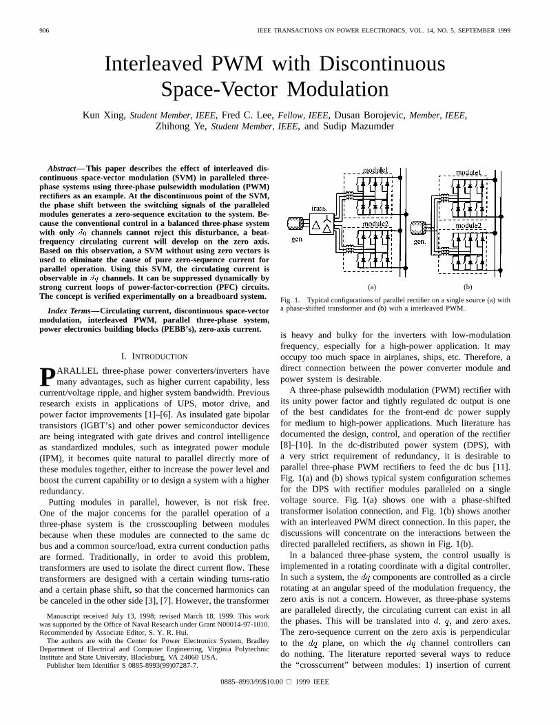
Fig. 1. Typical configurations of parallel rectifier on a single source (a) witha phase-shifted transformer and (b) with a interleaved PWM.
is heavy and bulky for the inverters with low-modulationfrequency, especially for a high-power application. It mayoccupy too much space in airplanes, ships, etc. Therefore, adirect connection between the power converter module andpower system is desirable.
A three-phase pulsewidth modulation (PWM) rectifier withits unity power factor and tightly regulated dc output is oneof the best candidates for the front-end dc power supplyfor medium to high-power applications. Much literature hasdocumented the design, control, and operation of the rectifier[8]–[10]. In the dc-distributed power system (DPS), witha very strict requirement of redundancy, it is desirable toparallel three-phase PWM rectifiers to feed the dc bus [11].Fig. 1(a) and (b) shows typical system configuration schemesfor the DPS with rectifier modules paralleled on a singlevoltage source. Fig. 1(a) shows one with a phase-shiftedtransformer isolation connection, and Fig. 1(b) shows anotherwith an interleaved PWM direct connection. In this paper, thediscussions will concentrate on the interactions between thedirected paralleled rectifiers, as shown in Fig. 1(b).
In a balanced three-phase system, the control usually isimplemented in a rotating coordinate with a digital controller.In such a system, the components are controlled as a circlerotating at an angular speed of the modulation frequency, thezero axis is not a concern. However, as three-phase systemsare paralleled directly, the circulating current can exist in allthe phases. This will be translated into and zero axes.The zero-sequence current on the zero axis is perpendicularto the plane, on which the channel controllers cando nothing. The literature reported several ways to reducethe “crosscurrent” between modules: 1) insertion of current
0885–8993/99$10.00 1999 IEEE
XING et al.: INTERLEAVED PWM WITH DISCONTINUOUS SPACE-VECTOR MODULATION 907
Fig. 2. System block diagram.
sharing reactors into the paralleled modules [1], [5], [6], [12],which includes two different cases, the coupled inductors areon the ac side for the VSI or the dc side for the CSI; 2)use of the “bang–bang” hysteresis control [3], which confinesthe current within a band by varying the switching frequency;and 3) use of a “combined-mode” current control [6], whichtreats the paralleled system as one system. The crosscurrentis compensated by choosing proper voltage vectors throughsensing the output current and their derivatives.
This paper looks for the control schemes for standardizedthree-phase modules. The module itself has a certain degreeof intelligence, the objective of the research is to make thesemodules able to “plug and play” without communicating witheach other. The desired features of such parallel modulesinclude: 1) use of constant frequency control and advancedmodulations techniques such as SVM; 2) keeping each moduleas independent as possible; and 3) having less communicationbetween modules. Through a comprehensive system analysisusing the averaged SVM model, this paper shows the mech-anism of how the zero-sequence current is produced with theinterleaved discontinuous SVM. It then investigates methods tomitigate the circulating current while maintaining each modulewith its own SVM, as with an individual module.
II. A NALYSIS OF THE CIRCULATING CURRENT
A. System Configuration
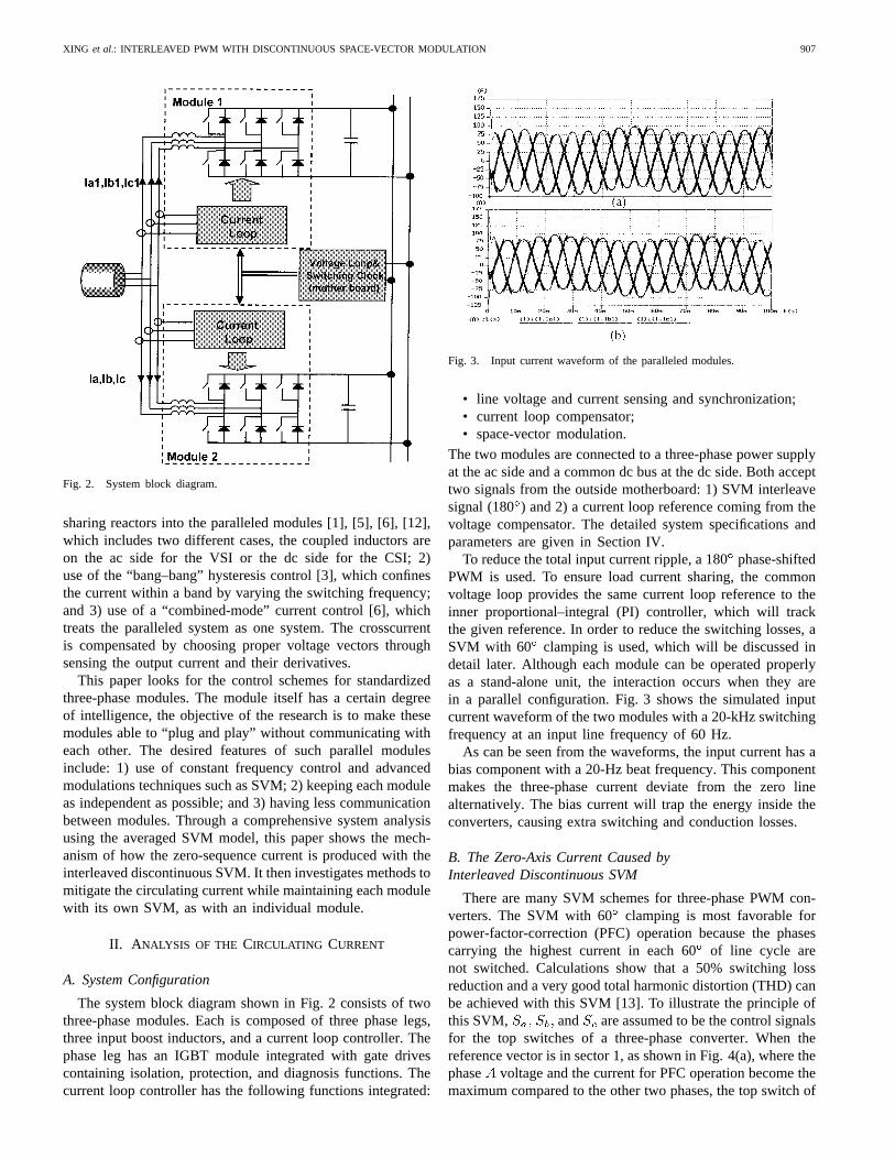
The system block diagram shown in Fig. 2 consists of twothree-phase modules. Each is composed of three phase legs,three input boost inductors, and a current loop controller. Thephase leg has an IGBT module integrated with gate drivescontaining isolation, protection, and diagnosis functions. Thecurrent loop controller has the following functions integrated:
Fig. 3. Input current waveform of the paralleled modules.
• line voltage and current sensing and synchronization;• current loop compensator;• space-vector modulation.
The two modules are connected to a three-phase power supplyat the ac side and a common dc bus at the dc side. Both accepttwo signals from the outside motherboard: 1) SVM interleavesignal (180) and 2) a current loop reference coming from thevoltage compensator. The detailed system specifications andparameters are given in Section IV.
To reduce the total input current ripple, a 180phase-shiftedPWM is used. To ensure load current sharing, the commonvoltage loop provides the same current loop reference to theinner proportional–integral (PI) controller, which will trackthe given reference. In order to reduce the switching losses, aSVM with 60 clamping is used, which will be discussed indetail later. Although each module can be operated properlyas a stand-alone unit, the interaction occurs when they arein a parallel configuration. Fig. 3 shows the simulated inputcurrent waveform of the two modules with a 20-kHz switchingfrequency at an input line frequency of 60 Hz.
As can be seen from the waveforms, the input current has abias component with a 20-Hz beat frequency. This componentmakes the three-phase current deviate from the zero linealternatively. The bias current will trap the energy inside theconverters, causing extra switching and conduction losses.
B. The Zero-Axis Current Caused byInterleaved Discontinuous SVM
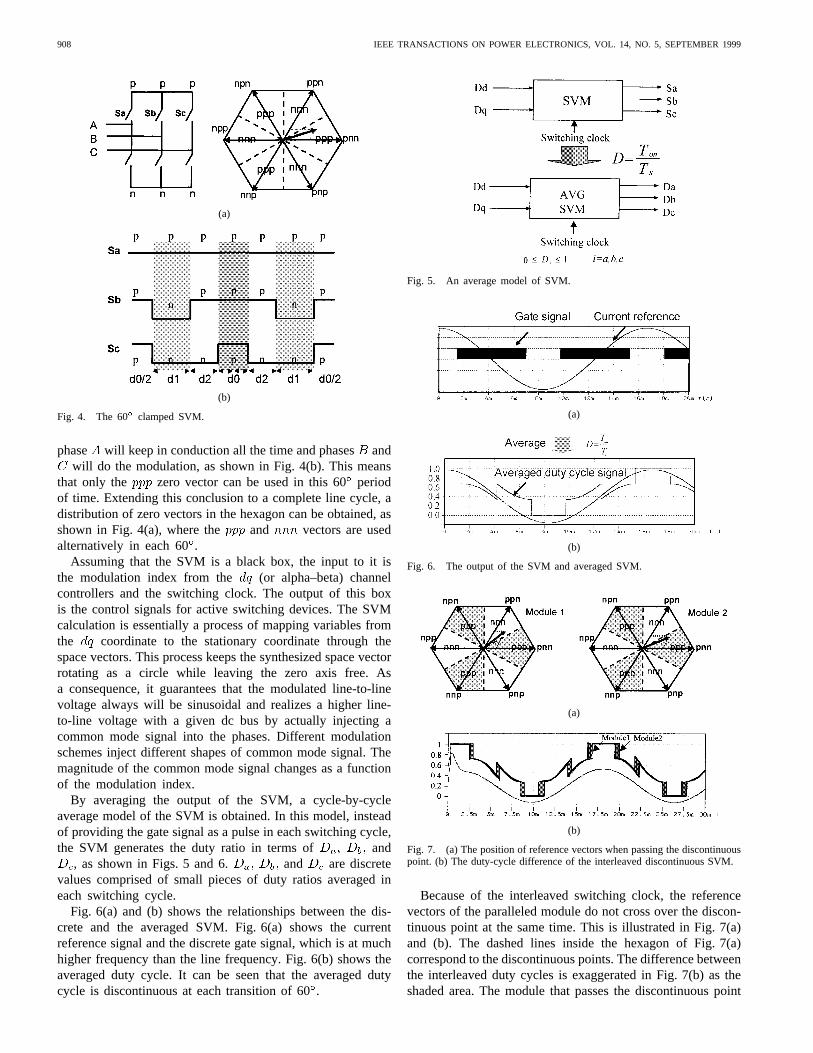
There are many SVM schemes for three-phase PWM con-verters. The SVM with 60 clamping is most favorable forpower-factor-correction (PFC) operation because the phasescarrying the highest current in each 60of line cycle arenot switched. Calculations show that a 50% switching lossreduction and a very good total harmonic distortion (THD) canbe achieved with this SVM [13]. To illustrate the principle ofthis SVM, and are assumed to be the control signalsfor the top switches of a three-phase converter. When thereference vector is in sector 1, as shown in Fig. 4(a), where thephase voltage and the current for PFC operation become themaximum compared to the other two phases, the top switch of
908 IEEE TRANSACTIONS ON POWER ELECTRONICS, VOL. 14, NO. 5, SEPTEMBER 1999
(a)
(b)
Fig. 4. The 60� clamped SVM.
phase will keep in conduction all the time and phasesandwill do the modulation, as shown in Fig. 4(b). This means
that only the zero vector can be used in this 60periodof time. Extending this conclusion to a complete line cycle, adistribution of zero vectors in the hexagon can be obtained, asshown in Fig. 4(a), where the and vectors are usedalternatively in each 60.
Assuming that the SVM is a black box, the input to it isthe modulation index from the (or alpha–beta) channelcontrollers and the switching clock. The output of this boxis the control signals for active switching devices. The SVMcalculation is essentially a process of mapping variables fromthe coordinate to the stationary coordinate through thespace vectors. This process keeps the synthesized space vectorrotating as a circle while leaving the zero axis free. Asa consequence, it guarantees that the modulated line-to-linevoltage always will be sinusoidal and realizes a higher line-to-line voltage with a given dc bus by actually injecting acommon mode signal into the phases. Different modulationschemes inject different shapes of common mode signal. Themagnitude of the common mode signal changes as a functionof the modulation index.
By averaging the output of the SVM, a cycle-by-cycleaverage model of the SVM is obtained. In this model, insteadof providing the gate signal as a pulse in each switching cycle,the SVM generates the duty ratio in terms of and
, as shown in Figs. 5 and 6. and are discretevalues comprised of small pieces of duty ratios averaged ineach switching cycle.
Fig. 6(a) and (b) shows the relationships between the dis-crete and the averaged SVM. Fig. 6(a) shows the currentreference signal and the discrete gate signal, which is at muchhigher frequency than the line frequency. Fig. 6(b) shows theaveraged duty cycle. It can be seen that the averaged dutycycle is discontinuous at each transition of 60.
Fig. 5. An average model of SVM.
(a)
(b)
Fig. 6. The output of the SVM and averaged SVM.
(a)
(b)
Fig. 7. (a) The position of reference vectors when passing the discontinuouspoint. (b) The duty-cycle difference of the interleaved discontinuous SVM.
Because of the interleaved switching clock, the referencevectors of the paralleled module do not cross over the discon-tinuous point at the same time. This is illustrated in Fig. 7(a)and (b). The dashed lines inside the hexagon of Fig. 7(a)correspond to the discontinuous points. The difference betweenthe interleaved duty cycles is exaggerated in Fig. 7(b) as theshaded area. The module that passes the discontinuous point
XING et al.: INTERLEAVED PWM WITH DISCONTINUOUS SPACE-VECTOR MODULATION 909
Fig. 8. The path of the pure zero-sequence current.
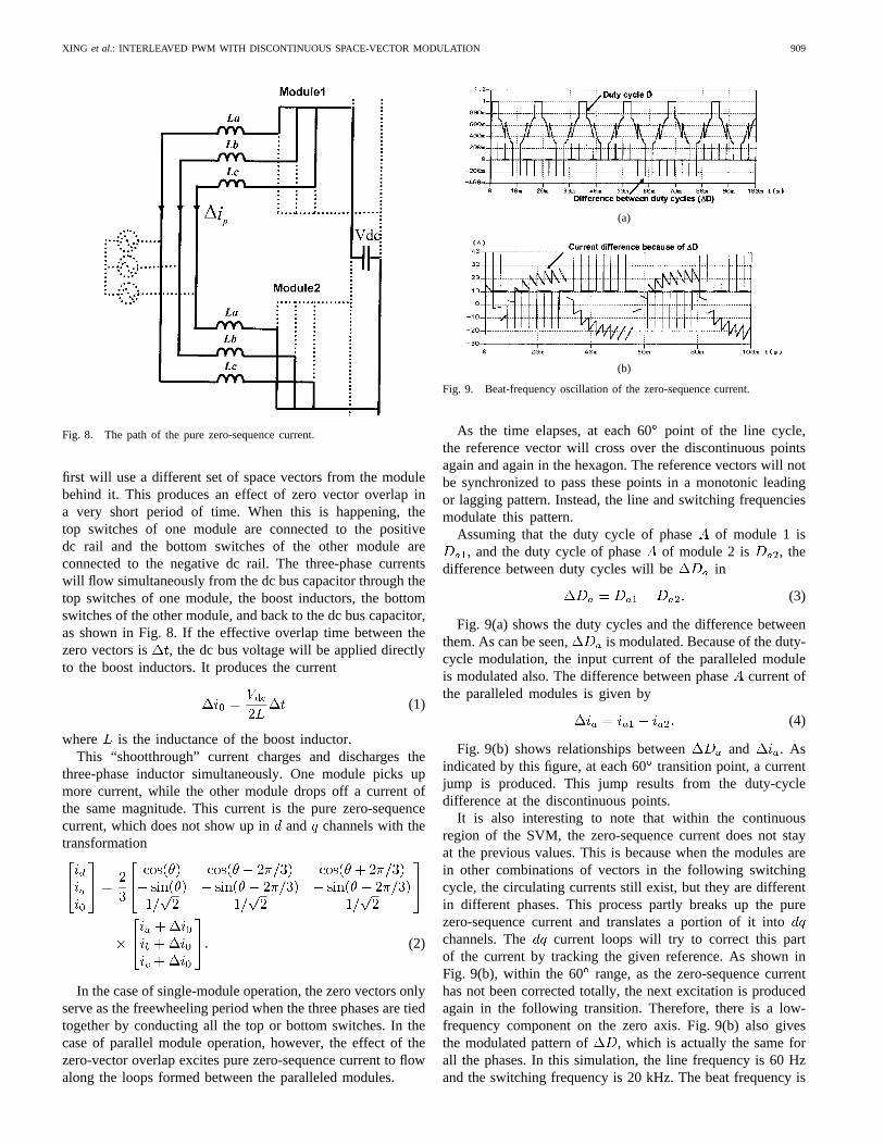
first will use a different set of space vectors from the modulebehind it. This produces an effect of zero vector overlap ina very short period of time. When this is happening, thetop switches of one module are connected to the positivedc rail and the bottom switches of the other module areconnected to the negative dc rail. The three-phase currentswill flow simultaneously from the dc bus capacitor through thetop switches of one module, the boost inductors, the bottomswitches of the other module, and back to the dc bus capacitor,as shown in Fig. 8. If the effective overlap time between thezero vectors is , the dc bus voltage will be applied directlyto the boost inductors. It produces the current
(1)
where is the inductance of the boost inductor.This “shootthrough” current charges and discharges the
three-phase inductor simultaneously. One module picks upmore current, while the other module drops off a current ofthe same magnitude. This current is the pure zero-sequencecurrent, which does not show up inand channels with thetransformation
(2)
In the case of single-module operation, the zero vectors onlyserve as the freewheeling period when the three phases are tiedtogether by conducting all the top or bottom switches. In thecase of parallel module operation, however, the effect of thezero-vector overlap excites pure zero-sequence current to flowalong the loops formed between the paralleled modules.
(a)
(b)
Fig. 9. Beat-frequency oscillation of the zero-sequence current.
As the time elapses, at each 60point of the line cycle,the reference vector will cross over the discontinuous pointsagain and again in the hexagon. The reference vectors will notbe synchronized to pass these points in a monotonic leadingor lagging pattern. Instead, the line and switching frequenciesmodulate this pattern.
Assuming that the duty cycle of phase of module 1 is, and the duty cycle of phase of module 2 is , the
difference between duty cycles will be in
(3)
Fig. 9(a) shows the duty cycles and the difference betweenthem. As can be seen, is modulated. Because of the duty-cycle modulation, the input current of the paralleled moduleis modulated also. The difference between phasecurrent ofthe paralleled modules is given by
(4)
Fig. 9(b) shows relationships between and . Asindicated by this figure, at each 60transition point, a currentjump is produced. This jump results from the duty-cycledifference at the discontinuous points.
It is also interesting to note that within the continuousregion of the SVM, the zero-sequence current does not stayat the previous values. This is because when the modules arein other combinations of vectors in the following switchingcycle, the circulating currents still exist, but they are differentin different phases. This process partly breaks up the purezero-sequence current and translates a portion of it intochannels. The current loops will try to correct this partof the current by tracking the given reference. As shown inFig. 9(b), within the 60 range, as the zero-sequence currenthas not been corrected totally, the next excitation is producedagain in the following transition. Therefore, there is a low-frequency component on the zero axis. Fig. 9(b) also givesthe modulated pattern of , which is actually the same forall the phases. In this simulation, the line frequency is 60 Hzand the switching frequency is 20 kHz. The beat frequency is
910 IEEE TRANSACTIONS ON POWER ELECTRONICS, VOL. 14, NO. 5, SEPTEMBER 1999
(a)
(b)
Fig. 10. (a) The effect of the pure zero-sequence current in time frame. (b)Three-dimensional (3-D) view of the three-phase current with a zero-sequencecurrent in the rotating frame.
20 Hz. The mathematical derivation of the modulated patternsof the duty-cycle difference is provided in Appendix A.
Assuming there is a common mode current riding on abalanced three-phase current as shown in
(5)
and
(6)
In the time frame, the three-phase current is depicted inFig. 10(a). By doing the transformation of
(7)
(8)
where the three-phase current can be mapped intoframeas shown in Fig. 10(b). The and components on theplane still rotate as a circle, but the zero-axis componentoscillates up and down. In a balanced three-phase system, onlytwo phases are independent because the sum of the voltageor current has to be zero. This is also true in the rotatingcoordinates. The controller can only control two of the three
(a)
(b)
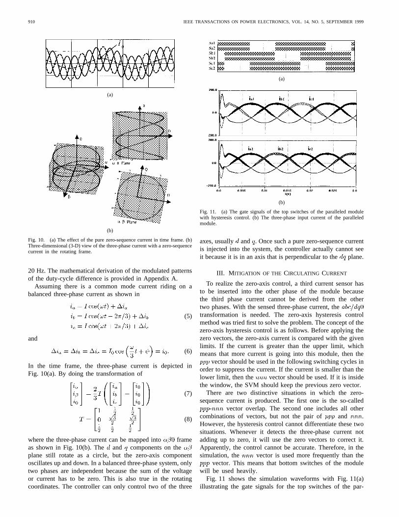
Fig. 11. (a) The gate signals of the top switches of the paralleled modulewith hysteresis control. (b) The three-phase input current of the paralleledmodule.
axes, usually and . Once such a pure zero-sequence currentis injected into the system, the controller actually cannot seeit because it is in an axis that is perpendicular to theplane.
III. M ITIGATION OF THE CIRCULATING CURRENT
To realize the zero-axis control, a third current sensor hasto be inserted into the other phase of the module becausethe third phase current cannot be derived from the othertwo phases. With the sensed three-phase current, thetransformation is needed. The zero-axis hysteresis controlmethod was tried first to solve the problem. The concept of thezero-axis hysteresis control is as follows. Before applying thezero vectors, the zero-axis current is compared with the givenlimits. If the current is greater than the upper limit, whichmeans that more current is going into this module, then the
vector should be used in the following switching cycles inorder to suppress the current. If the current is smaller than thelower limit, then the vector should be used. If it is insidethe window, the SVM should keep the previous zero vector.
There are two distinctive situations in which the zero-sequence current is produced. The first one is the so-called
- vector overlap. The second one includes all othercombinations of vectors, but not the pair of and .However, the hysteresis control cannot differentiate these twosituations. Whenever it detects the three-phase current notadding up to zero, it will use the zero vectors to correct it.Apparently, the control cannot be accurate. Therefore, in thesimulation, the vector is used more frequently than the
vector. This means that bottom switches of the modulewill be used heavily.
Fig. 11 shows the simulation waveforms with Fig. 11(a)illustrating the gate signals for the top switches of the par-
XING et al.: INTERLEAVED PWM WITH DISCONTINUOUS SPACE-VECTOR MODULATION 911
alleled module and Fig. 11(b) the input current waveform ofthe paralleled module. As a result of the biased use of theswitches, the input current is affected. The positive portionof the current has more ripples than the negative portion, asshown in Fig. 11(b). Therefore, this control strategy is notvery desirable.
As we have noted earlier, the zero-sequence current pro-duced at the discontinuous points does not hold at the samevalue in the following 60 period, but tends to return to thezero, which is seemingly in contradiction with the statementthat the channel cannot reject the zero axis current. Ac-tually, the current loops are doing their jobs. Assuming bothreference vectors are in sector 1, where the , andvectors are used, within a switching cycle, there will be sometime intervals when the two modules use different vectors. Forexample, one module is in the vector, while the other isin either the or vector. Therefore, there will be aphase, either or , to participate in the current circulation,which breaks up the existing pure zero-sequence current andtranslates a portion of it into the and axes, where theand axes controllers can see them. Because of the intendedPWM interleaving, the current circulation will not stop as longas the modules are not in the same vector. Therefore, it isimpossible to make the sum of the three-phase current be zeroat the switching frequency. The goal is to control its averagevalue so that it does not accumulate.
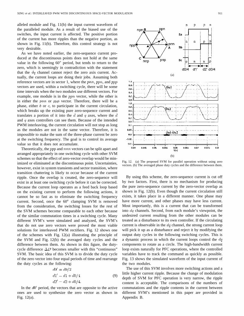
Theoretically, the and vectors can be split apart andarranged appropriately in one switching cycle with other SVMschemes so that the effect of zero-vector overlap would be min-imized or eliminated at the discontinuous point. Uncertainties,however, exist in system transients and sector transition, wheretransition chattering is likely to occur because of the currentripple. Once the overlap is created, the zero-sequence willexist in at least one switching cycle before it can be corrected.Because the current loop operates as a feed back loop basedon the existing current to perform the following actions, itcannot be so fast as to eliminate the switching frequencycurrent. Second, once the 60clamping SVM is removedfrom the consideration, the switching losses for the rest ofthe SVM schemes become comparable to each other becauseof the similar commutation times in a switching cycle. Manydifferent SVM’s were simulated and analyzed, the SVM’sthat do not use zero vectors were proved the most viablesolutions for interleaved PWM rectifiers. Fig. 12 shows oneof the schemes with Fig. 12(a) illustrating the principle ofthe SVM and Fig. 12(b) the averaged duty cycles and thedifference between them. As shown in this figure, the duty-cycle difference becomes smaller with this “continuous”SVM. The basic idea of this SVM is to divide the duty cycleof the zero vector into four equal periods of time and rearrangethe duty cycles as the following:
(9)
In the period, the vectors that are opposite to the activeones are used to synthesize the zero vector as shown inFig. 12(a).
(a)
(b)
Fig. 12. (a) The proposed SVM for parallel operation without using zerovectors. (b) The averaged phase duty cycles and the difference between them.
By using this scheme, the zero-sequence current is cut offby two factors. First, there is no mechanism for producingthe pure zero-sequence current by the zero-vector overlap asshown in Fig. 12(b). Even though the current circulation stillexists, it takes place in a different manner. One phase mayhave more current, and other phases may have less current.Most importantly, this is a current that can be transformedinto channels. Second, from each module’s viewpoint, theundesired current resulting from the other modules can betreated as a disturbance to its own controller. If the circulatingcurrent is observable in the channel, the strong current loopwill pick it up as a disturbance and reject it by modifying theoutput duty cycles in the following switching cycles. This isa dynamic process in which the current loops control thecomponents to rotate as a circle. The high-bandwidth currentloop exists naturally for PFC operations, where the controlledvariables have to track the command as quickly as possible.Fig. 13 shows the simulated waveform of the input current ofthe two modules.
The use of this SVM involves more switching actions and alittle higher current ripple. Because the change of modulationdepth of SVM for PFC operation is very narrow, the ripplecontent is acceptable. The comparisons of the numbers ofcommutations and the ripple contents in the current betweendifferent SVM’s mentioned in this paper are provided inAppendix B.
912 IEEE TRANSACTIONS ON POWER ELECTRONICS, VOL. 14, NO. 5, SEPTEMBER 1999
Fig. 13. Three-phase input current with the proposed SVM.
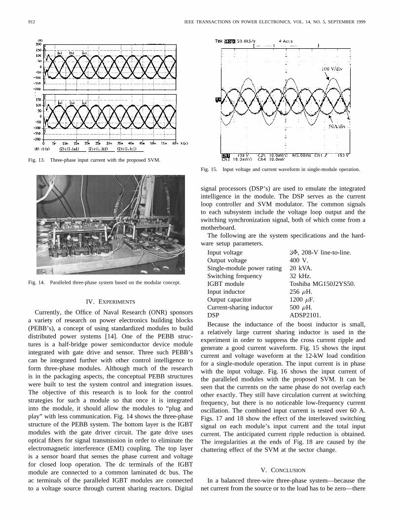
Fig. 14. Paralleled three-phase system based on the modular concept.
IV. EXPERIMENTS
Currently, the Office of Naval Research (ONR) sponsorsa variety of research on power electronics building blocks(PEBB’s), a concept of using standardized modules to builddistributed power systems [14]. One of the PEBB struc-tures is a half-bridge power semiconductor device moduleintegrated with gate drive and sensor. Three such PEBB’scan be integrated further with other control intelligence toform three-phase modules. Although much of the researchis in the packaging aspects, the conceptual PEBB structureswere built to test the system control and integration issues.The objective of this research is to look for the controlstrategies for such a module so that once it is integratedinto the module, it should allow the modules to “plug andplay” with less communication. Fig. 14 shows the three-phasestructure of the PEBB system. The bottom layer is the IGBTmodules with the gate driver circuit. The gate drive usesoptical fibers for signal transmission in order to eliminate theelectromagnetic interference (EMI) coupling. The top layeris a sensor board that senses the phase current and voltagefor closed loop operation. The dc terminals of the IGBTmodule are connected to a common laminated dc bus. Theac terminals of the paralleled IGBT modules are connectedto a voltage source through current sharing reactors. Digital
Fig. 15. Input voltage and current waveform in single-module operation.
signal processors (DSP’s) are used to emulate the integratedintelligence in the module. The DSP serves as the currentloop controller and SVM modulator. The common signalsto each subsystem include the voltage loop output and theswitching synchronization signal, both of which come from amotherboard.
The following are the system specifications and the hard-ware setup parameters.
Input voltage , 208-V line-to-line.Output voltage 400 V.Single-module power rating 20 kVA.Switching frequency 32 kHz.IGBT module Toshiba MG150J2YS50.Input inductor 256 H.Output capacitor 1200 F.Current-sharing inductor 500H.DSP ADSP2101.
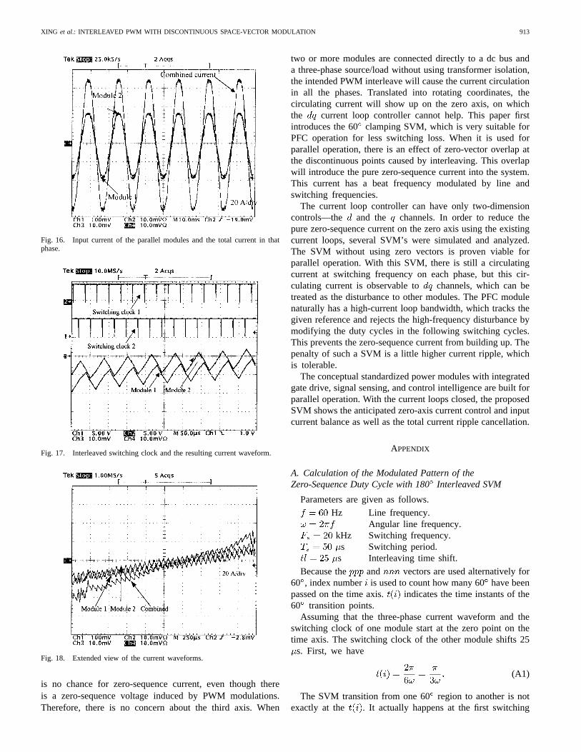
Because the inductance of the boost inductor is small,a relatively large current sharing inductor is used in theexperiment in order to suppress the cross current ripple andgenerate a good current waveform. Fig. 15 shows the inputcurrent and voltage waveform at the 12-kW load conditionfor a single-module operation. The input current is in phasewith the input voltage. Fig. 16 shows the input current ofthe paralleled modules with the proposed SVM. It can beseen that the currents on the same phase do not overlap eachother exactly. They still have circulation current at switchingfrequency, but there is no noticeable low-frequency currentoscillation. The combined input current is tested over 60 A.Figs. 17 and 18 show the effect of the interleaved switchingsignal on each module’s input current and the total inputcurrent. The anticipated current ripple reduction is obtained.The irregularities at the ends of Fig. 18 are caused by thechattering effect of the SVM at the sector change.
V. CONCLUSION
In a balanced three-wire three-phase system—because thenet current from the source or to the load has to be zero—there
XING et al.: INTERLEAVED PWM WITH DISCONTINUOUS SPACE-VECTOR MODULATION 913
Fig. 16. Input current of the parallel modules and the total current in thatphase.
Fig. 17. Interleaved switching clock and the resulting current waveform.
Fig. 18. Extended view of the current waveforms.
is no chance for zero-sequence current, even though thereis a zero-sequence voltage induced by PWM modulations.Therefore, there is no concern about the third axis. When
two or more modules are connected directly to a dc bus anda three-phase source/load without using transformer isolation,the intended PWM interleave will cause the current circulationin all the phases. Translated into rotating coordinates, thecirculating current will show up on the zero axis, on whichthe current loop controller cannot help. This paper firstintroduces the 60clamping SVM, which is very suitable forPFC operation for less switching loss. When it is used forparallel operation, there is an effect of zero-vector overlap atthe discontinuous points caused by interleaving. This overlapwill introduce the pure zero-sequence current into the system.This current has a beat frequency modulated by line andswitching frequencies.
The current loop controller can have only two-dimensioncontrols—the and the channels. In order to reduce thepure zero-sequence current on the zero axis using the existingcurrent loops, several SVM’s were simulated and analyzed.The SVM without using zero vectors is proven viable forparallel operation. With this SVM, there is still a circulatingcurrent at switching frequency on each phase, but this cir-culating current is observable to channels, which can betreated as the disturbance to other modules. The PFC modulenaturally has a high-current loop bandwidth, which tracks thegiven reference and rejects the high-frequency disturbance bymodifying the duty cycles in the following switching cycles.This prevents the zero-sequence current from building up. Thepenalty of such a SVM is a little higher current ripple, whichis tolerable.
The conceptual standardized power modules with integratedgate drive, signal sensing, and control intelligence are built forparallel operation. With the current loops closed, the proposedSVM shows the anticipated zero-axis current control and inputcurrent balance as well as the total current ripple cancellation.
APPENDIX
A. Calculation of the Modulated Pattern of theZero-Sequence Duty Cycle with 180Interleaved SVM
Parameters are given as follows.
Hz Line frequency.Angular line frequency.
kHz Switching frequency.s Switching period.
s Interleaving time shift.
Because the and vectors are used alternatively for60 , index number is used to count how many 60have beenpassed on the time axis. indicates the time instants of the60 transition points.
Assuming that the three-phase current waveform and theswitching clock of one module start at the zero point on thetime axis. The switching clock of the other module shifts 25
s. First, we have
(A1)
The SVM transition from one 60region to another is notexactly at the . It actually happens at the first switching
914 IEEE TRANSACTIONS ON POWER ELECTRONICS, VOL. 14, NO. 5, SEPTEMBER 1999
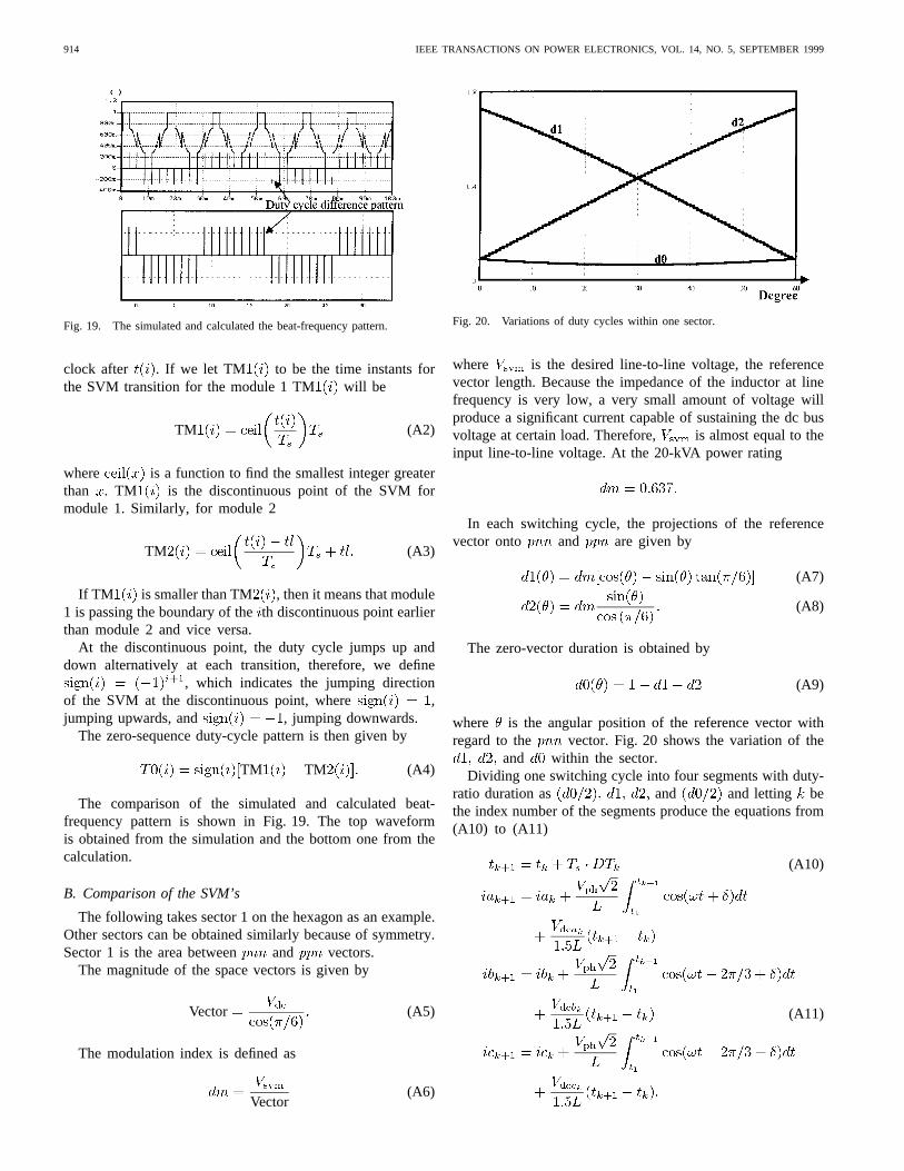
Fig. 19. The simulated and calculated the beat-frequency pattern.
clock after . If we let TM to be the time instants forthe SVM transition for the module 1 TM will be
TM (A2)
where is a function to find the smallest integer greaterthan . TM is the discontinuous point of the SVM formodule 1. Similarly, for module 2
TM (A3)
If TM is smaller than TM , then it means that module1 is passing the boundary of theth discontinuous point earlierthan module 2 and vice versa.
At the discontinuous point, the duty cycle jumps up anddown alternatively at each transition, therefore, we define
, which indicates the jumping directionof the SVM at the discontinuous point, where ,jumping upwards, and , jumping downwards.
The zero-sequence duty-cycle pattern is then given by
TM TM (A4)
The comparison of the simulated and calculated beat-frequency pattern is shown in Fig. 19. The top waveformis obtained from the simulation and the bottom one from thecalculation.
B. Comparison of the SVM’s
The following takes sector 1 on the hexagon as an example.Other sectors can be obtained similarly because of symmetry.Sector 1 is the area between and vectors.
The magnitude of the space vectors is given by
Vector (A5)
The modulation index is defined as
Vector(A6)
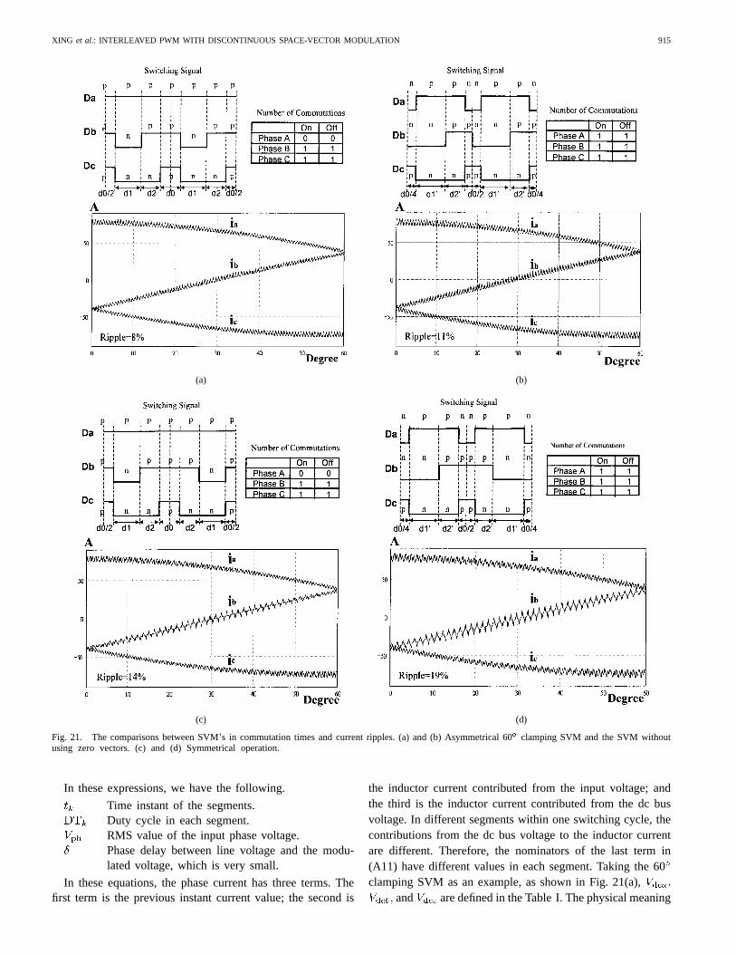
Fig. 20. Variations of duty cycles within one sector.
where is the desired line-to-line voltage, the referencevector length. Because the impedance of the inductor at linefrequency is very low, a very small amount of voltage willproduce a significant current capable of sustaining the dc busvoltage at certain load. Therefore, is almost equal to theinput line-to-line voltage. At the 20-kVA power rating
In each switching cycle, the projections of the referencevector onto and are given by
(A7)
(A8)
The zero-vector duration is obtained by
(A9)
where is the angular position of the reference vector withregard to the vector. Fig. 20 shows the variation of the
and within the sector.Dividing one switching cycle into four segments with duty-
ratio duration as and and letting bethe index number of the segments produce the equations from(A10) to (A11)
(A10)
(A11)
XING et al.: INTERLEAVED PWM WITH DISCONTINUOUS SPACE-VECTOR MODULATION 915
(a) (b)
(c) (d)
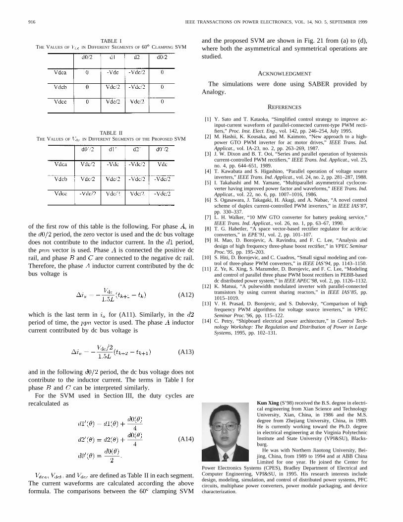
Fig. 21. The comparisons between SVM’s in commutation times and current ripples. (a) and (b) Asymmetrical 60� clamping SVM and the SVM withoutusing zero vectors. (c) and (d) Symmetrical operation.
In these expressions, we have the following.
Time instant of the segments.Duty cycle in each segment.RMS value of the input phase voltage.Phase delay between line voltage and the modu-lated voltage, which is very small.
In these equations, the phase current has three terms. Thefirst term is the previous instant current value; the second is
the inductor current contributed from the input voltage; andthe third is the inductor current contributed from the dc busvoltage. In different segments within one switching cycle, thecontributions from the dc bus voltage to the inductor currentare different. Therefore, the nominators of the last term in(A11) have different values in each segment. Taking the 60clamping SVM as an example, as shown in Fig. 21(a),
and are defined in the Table I. The physical meaning
916 IEEE TRANSACTIONS ON POWER ELECTRONICS, VOL. 14, NO. 5, SEPTEMBER 1999
TABLE ITHE VALUES OF Vdc IN DIFFERENT SEGMENTS OF60� CLAMPING SVM
TABLE IITHE VALUES OF Vdc IN DIFFERENT SEGMENTS OF THEPROPOSEDSVM
of the first row of this table is the following. For phase, inthe period, the zero vector is used and the dc bus voltagedoes not contribute to the inductor current. In theperiod,the vector is used. Phase is connected the positive dcrail, and phase and are connected to the negative dc rail.Therefore, the phase inductor current contributed by the dcbus voltage is
(A12)
which is the last term in for (A11). Similarly, in theperiod of time, the vector is used. The phase inductorcurrent contributed by dc bus voltage is
(A13)
and in the following period, the dc bus voltage does notcontribute to the inductor current. The terms in Table I forphase and can be interpreted similarly.
For the SVM used in Section III, the duty cycles arerecalculated as
(A14)
and are defined as Table II in each segment.The current waveforms are calculated according the aboveformula. The comparisons between the 60clamping SVM
and the proposed SVM are shown in Fig. 21 from (a) to (d),where both the asymmetrical and symmetrical operations arestudied.
ACKNOWLEDGMENT
The simulations were done using SABER provided byAnalogy.
REFERENCES
[1] Y. Sato and T. Kataoka, “Simplified control strategy to improve ac-input-current waveform of parallel-connected current-type PWM recti-fiers,” Proc. Inst. Elect. Eng., vol. 142, pp. 246–254, July 1995.
[2] M. Hashii, K. Kousaka, and M. Kaimoto, “New approach to a high-power GTO PWM inverter for ac motor drives,”IEEE Trans. Ind.Applicat., vol. IA-23, no. 2, pp. 263–269, 1987.
[3] J. W. Dixon and B. T. Ooi, “Series and parallel operation of hysteresiscurrent-controlled PWM rectifiers,”IEEE Trans. Ind. Applicat., vol. 25,no. 4, pp. 644–651, 1989.
[4] T. Kawabata and S. Higashino, “Parallel operation of voltage sourceinverters,”IEEE Trans. Ind. Applicat., vol. 24, no. 2, pp. 281–287, 1988.
[5] I. Takahashi and M. Yamane, “Multiparallel asymmetrical cyclocon-verter having improved power factor and waveforms,”IEEE Trans. Ind.Applicat., vol. 22, no. 6, pp. 1007–1016, 1986.
[6] S. Ogasawara, J. Takagaki, H. Akagi, and A. Nabae, “A novel controlscheme of duplex current-controlled PWM inverters,” inIEEE IAS’87,pp. 330–337.
[7] L. H. Walker, “10 MW GTO converter for battery peaking service,”IEEE Trans. Ind. Applicat., vol. 26, no. 1, pp. 63–67, 1990.
[8] T. G. Habetler, “A space vector-based rectifier regulator for ac/dc/acconverters,” inEPE’91, vol. 2, pp. 101–107.
[9] H. Mao, D. Borojevic, A. Ravindra, and F. C. Lee, “Analysis anddesign of high frequency three-phase boost rectifier,” inVPEC SeminarProc.’95, pp. 195–203.
[10] S. Hiti, D. Borojevic, and C. Cuadros, “Small signal modeling and con-trol of three-phase PWM converters,” inIEEE IAS’94, pp. 1143–1150.
[11] Z. Ye, K. Xing, S. Mazumder, D. Borojevic, and F. C. Lee, “Modelingand control of parallel three phase PWM boost rectifiers in PEBB-baseddc distributed power system,” inIEEE APEC’98, vol. 2, pp. 1126–1132.
[12] K. Matsui, “A pulsewidth modulated inverter with parallel-connectedtransistors by using current sharing reactors,” inIEEE IAS’85, pp.1015–1019.
[13] V. H. Prasad, D. Borojevic, and S. Dubovsky, “Comparison of highfrequency PWM algorithms for voltage source inverters,” inVPECSeminar Proc.’96, pp. 115–122.
[14] C. Petry, “Shipboard electrical power architecture,” inControl Tech-nology Workshop: The Regulation and Distribution of Power in LargeSystems, 1995, pp. 102–131.
Kun Xing (S’98) received the B.S. degree in electri-cal engineering from Xian Science and TechnologyUniversity, Xian, China, in 1986 and the M.S.degree from Zhejiang University, China, in 1989.He is currently working toward the Ph.D. degreein electrical engineering at the Virginia PolytechnicInstitute and State University (VPI&SU), Blacks-burg.
He was with Northern Jiaotong University, Bei-jing, China, from 1989 to 1994 and at ABB ChinaLimited for one year. He joined the Center for
Power Electronics Systems (CPES), Bradley Department of Electrical andComputer Engineering, VPI&SU, in 1995. His research interests includedesign, modeling, simulation, and control of distributed power systems, PFCcircuits, multiphase power converters, power module packaging, and devicecharacterization.

XING et al.: INTERLEAVED PWM WITH DISCONTINUOUS SPACE-VECTOR MODULATION 917
Fred C. Lee (S’72–M’74–SM’87–F’90) receivedthe B.S. degree in electrical engineering from theNational Cheng Kung University, Taiwan, R.O.C.,in 1968 and the M.S. and Ph.D. degrees fromDuke University, Durham, NC, in 1971 and 1974,respectively.
He holds the Lewis A. Hester Chair of Engi-neering at the Virginia Polytechnic Institute andState University (VPI&SU), Blacksburg, and wasthe James S. Tucker Endowed Professor in theBradley Department of Electrical Engineering. He is
the Founder and Director of the Virginia Power Electronics Center (VPEC),a Technology Development Center of the Virginia’s Center for InnovativeTechnology (CIT). Under his leadership, VPEC has become one of thelargest university-based power electronics research centers in the country.His research interests include: high-frequency power conversion, distributedpower systems, space power systems, PFC techniques, electronics packaging,high-frequency magnetics, device characterization, and modeling and controlof converters.
Dr. Lee served as the President of the IEEE Power Electronics Society from1993 to 1994. He was a recipient of the 1985 Ralph R. Teeter EducationalAward, the 1990 Alumni Award for research excellence from VPI&SU, andthe PCIM Award for Leadership in Power Electronics Education in 1990.He is also the recipient of the 1989 William E. Newell Power ElectronicsAward, the highest award presented by the IEEE Power Electronics Societyfor outstanding achievement in power electronics.
Dusan Boroyevich (M’82) received the B.S. de-gree from the University of Belgrade, Belgrade,Yugoslavia, in 1976, the M.S. degree from theUniversity of Novi Sad, Novi Sad, Yugoslavia, in1982, and the Ph.D. degree from the Virginia Poly-technic Institute and State University (VPI&SU),Blacksburg, in 1986.
From 1986 to 1990, he was an Assistant Professorand Director of the Power and Industrial ElectronicsResearch Program at the Institute for Power andElectronics Engineering, University of Novi Sad. In
1989, he was Acting Head of the Institute. In 1990, he joined VPI&SU as anAssociate Professor and in 1996 became Associate Director of the VirginiaPower Electronics Center. His research interests include multiphase powerconversion, high-power PWM converters, modeling and control of powerconverters, applied digital control, and electrical drives. He has published over100 technical papers, has three patents, and has advised three Ph.D. and sixM.S. students to completion. He has been involved in numerous governmentand industry-sponsored research projects in the areas of power and industrialelectronics, totaling over $5 million.
Dr. Boroyevich is a member of the IEEE Power Electronics Society AdCom,IEEE Industry Applications Society, and the Industrial Drives and IndustrialPower Converter Committees. He is also a member of the Phi Kappa Phihonor society.
Zhihong Ye (S’98) received the B.S. and M.S.degrees in electrical engineering from Tsinghua Uni-versity, Beijing, China, in 1992 and 1994, respec-tively. He is currently working toward the Ph.D.degree at the Virginia Polytechnic Institute and StateUniversity (VPI&SU), Blacksburg.
From 1994 to 1996, he was a Research Assis-tant with the Department of Electrical and AppliedElectronics Engineering, Tsinghua University. Hisresearch interests are three-phase power convertersmodeling and control and stability and interaction
analysis of distributed power electronics systems.
Sudip Mazumder received the M.S. degree inelectrical power engineering from the RensselaerPolytechnic Institute, Troy, NY, in 1993. He iscurrently working towards the Ph.D. degree at theVirginia Polytechnic Institute and State University(VPI&SU), Blacksburg.
He has eight years of industrial experience inthe area of motor drives and power electronics. Hisareas of interest include nonlinear analysis and non-linear control of dc and multiphase multistage con-verters, high-performance motor drives, and bidi-
rectional and soft-switch converters.


![Chapter 5 SPACE VECTOR PWM - · PDF file175 Chapter 5 SPACE VECTOR PWM 5.1 5.2 Introduction The space vector PWM (SVPWM) [5.1] is an alternative method used to control three](https://img.pdfslide.us/doc/110x75/5a76cdea7f8b9a1b688d899f/chapter-5-space-vector-pwm-fleadh-175-chapter-5-space-vector-pwm-51-52-introduction.jpg)