Embed Size (px)
Citation preview

1
Modified Discontinuous PWM for Size Reductionof the Circulating Current Filter in Parallel
Interleaved ConvertersGhanshyamsinh Gohil, Student Member, IEEE, RamKrishan Maheshwari, Member, IEEE, Lorand Bede, StudentMember, IEEE, Tamas Kerekes, Member, IEEE, Remus Teodorescu, Fellow, IEEE, Marco Liserre, Fellow, IEEE,
and Frede Blaabjerg, Fellow, IEEE
Abstract—Parallel Voltage Source Converters (VSCs) requirean inductive filter to suppress the circulating current. The sizeof this filter can be minimized by reducing either the maximumvalue of the flux linkage or the core losses. This paper presents amodified Discontinuous Pulsewidth Modulation (DPWM) schemeto reduce the maximum value of the flux linkage and the corelosses in the circulating current filter. In the proposed PWMscheme, the dwell time of an active vector is divided within ahalf-carrier cycle to ensure simultaneous occurrence of the samezero vectors in both VSCs. A function to decide the ratio of thedwell time of the divided active vector is also presented. The effectof the proposed PWM scheme on the maximum value of the fluxlinkage and the core losses is analyzed and compared with that ofthe space vector modulation and 60clamped DPWM schemes.The analytical expressions for the maximum value of the fluxlinkage are derived for each of these PWM schemes. In addition,the effect of the proposed PWM scheme on the line current rippleand the switching losses is also analyzed and compared. To verifythe analysis, experimental results are presented, which prove theeffectiveness of the proposed PWM scheme.
I. INTRODUCTION
Three-phase voltage source converter (VSC) is widely usedas a dc/ac converter in power electronics applications andoften connected in parallel to meet the ever increasing demandfor higher power rating converter [1], [2]. In grid-connectedapplication, the total harmonic distortion (THD) in the linecurrent should be low [3]. Due to limited switching frequencyin the high power converters, large filters are required [4].This leads to the increase in the size, weight, and cost ofthe overall converter system. For VSC fed variable speedmachines, the harmonic distortion in the line current must below for satisfactory operation of the drive [5]. The harmonicdistortion depends primarily on the switching sequence, mod-ulation index, and the switching frequency [5]. Several effortshave been made to improve the performance of the VSC interms of the harmonic distortion and switching losses by usingoptimal switching sequences for modulation of the VSC legs[6]–[8].
The harmonic distortion in the line current can be reducedby increasing the switching frequency. However, the switchingfrequency of the semiconductor devices for high power appli-cations is often limited. The effective switching frequency canbe increased by using interleaved carriers in parallel-connectedVSCs, and the line current quality can be improved [9]. Theselection of the proper interleaving angle leads to the reduction
Vdc2
Vdc2
IA1
IB1
IC1
IA2
IB2
IC2
Filter
A1
B1
C1
A2
B2
C2
IA
IB
IC
Load
Load
Load
N
Linefilter
Coupledinductor
X
IX1
IX2
IXIX,c
IBn
IAn
ICn
Linefilter
Common-modeinductor
A
B
C
An
Bn
Cn
X1
X2
A
B
C
O
Fig. 1. Two parallel interleaved VSCs with a common dc-link. The filterarrangement for circulating current suppression using the CI and the CMinductor is depicted, where X = A,B,C and n = 1, 2.
in the line current ripple [9]–[15]. This implies that withinterleaved parallel VSCs, the size of the line filter can bereduced, or the switching frequency can be reduced for a givenset of filter components without violating the THD constraints.
The circulating current is generated in the parallel VSCsdue to hardware and control asymmetries [2]. When carrierinterleaving is used, the pole voltages (measured with respectto the fictitious mid-point of the dc-link O, as shown in Fig.1) of the interleaved parallel legs are phase shifted. Therefore,there exists a potential difference that further increases thecirculating current [16]. This is a high frequency circulatingcurrent with harmonic components concentrated around theodd multiples of the switching frequency [12]. This unwantedcurrent increases stress on the semiconductor switches andcauses additional losses. Therefore, it should be suppressed.
The circulating current is strongly influenced by thePulsewidth Modulation (PWM) scheme. The conventionalSpace Vector Modulation (SVM) uses two adjacent activevectors and both of the zero vectors to synthesize a referencespace vector. The zero vectors are applied at the beginning andat the end of a half-carrier cycle. Various other variants of the

2
SVM scheme can be obtained by merely dividing the dwelltime of the zero vectors unequally [17]. The DiscontinuousPWM (DPWM) schemes use only one zero vector in each half-carrier cycle. The commutation of each phase leg is ceasedfor the one third period of the fundamental cycle [18], [19].The PWM schemes, which modify the DPWM schemes bydividing one of the active vectors into two equal halves, areproposed in [20], [21]. These PWM schemes affect the linecurrent ripple. A hybrid PWM scheme, which is a combinationof the conventional SVM and different DPWM schemes, isproposed in [14] to minimize the line current ripple for theparallel VSCs. However, separate dc-links are used and thusthe circulating current filter is not present.
To avoid the circulating current, galvanic isolated trans-former can be used for each VSC [22]. However, the use ofthe bulky transformer adds to the cost and increases the size.Therefore, it should be avoided. Instead of this, a coupledinductor (CI) [23]–[26] for each phase or a common-mode(CM) [27] inductor for each VSC can be used as a circulatingcurrent filter (Fig. 1). Assuming strong magnetic coupling inthe circulating current filter, the flux linkage in the core due tothe line current can be neglected. Therefore, the flux linkagehas only the high frequency components determined by theswitching frequency. These high frequency components resultin high core losses, and the circulating current filter requireslarger surface area to dissipate the heat. Ewanchuk et al. [28]proposed a modified DPWM scheme that can make the CMvoltage zero. This permits the use of a three limb inductoronly. However, the number of commutations are increased.Therefore, it may not be feasible for medium/high powerapplications. Another PWM scheme is proposed in [29] tochange the zero vector pattern by introducing an additionalswitching. This avoids the coexistence of the different zerovectors at a sector transition, and thus the jumping of thecirculating current can be avoided.
The CI is used to provide magnetic coupling between theparallel interleaved legs [23]–[26]. A modified CI, which isproposed in [30], combines the functionality of both the linefilter inductor and the circulating current filter. To reduce theflux linkage in the CI, a PWM scheme is proposed in [25].This PWM scheme adds an optimal common-mode offset tothe reference signals based on the modulation index. This canlead to the reduction of the maximum value of the flux linkage,but the discussion on the core losses is not given. However,the core losses are an important parameter to consider in thedesign of the circulating current filter. As discussed before,the high frequency components of the flux linkage increasethe core losses. This may lead to a thermally limited design ofthe circulating current filter, where the maximum flux densityin the core is limited by the heat dissipation capability andnot by the magnetic saturation. In this case, the core lossescan be reduced by reducing the peak flux density for a givenswitching frequency and core dimensions.
An active method to reduce the peak flux linkage as well asthe core losses for the circulating current filter is proposedin this paper. The method divides the dwell time of anactive vector within a half-carrier cycle to ensure simultaneousoccurrence of the same zero vectors in both VSCs. A function
to calculate the division of the dwell time are also proposed.This reduces both the maximum value of the flux linkage andthe core losses in the circulating current filter.
The paper is organized as follows. Section II presentsthe basic theory of the circulating current. In addition, therelationship between the flux linkage in the circulating currentfilter and the pole voltages is discussed for the interleavedVSCs. The effect of the different switching sequences on theflux linkage in the core is analyzed in Section III. SectionIV presents the proposed DPWM scheme. The effect of theproposed PWM on the flux linkage in the CI and the CMinductor, the harmonic distortion in the line current, and theswitching losses are also discussed and compared with thatof the SVM and the 60 clamped DPWM. The experimentalresults are presented in Section V.
II. PARALLEL INTERLEAVED VSCS
A. Circulating Current
The parallel-connected VSCs are operated with interleavedcarrier signals. The circulating current (IX,c) flows throughthe VSC legs in addition to the line current component IX1,l,as shown in Fig. 1. Therefore, the phase currents can be givenby
IX1 = IX1,l + IX,c
IX2 = IX2,l − IX,c(1)
where IX1,l and IX2,l are the components of the phasecurrents contributing to the resultant line current IX . IX,cis the circulating current, where X = A,B,C. Assumingideal VSCs and neglecting the effect of the hardware/controlasymmetries, the current component of each VSC, contributingto the grid current, are considered to be equal (IX1,l = IX2,l).Therefore,
IX,c =IX1 − IX2
2(2)
The differential equation describing phase X circulatingcurrent can be given as
dIX,cdt
=VX1O − VX2O
Lc(3)
where Lc is the inductance offered to the circulating current.VX1O and VX2O are the pole voltages measured with respectto the fictitious dc-link mid point O.
B. Flux Linkage in Circulating Current Filter
To offer the desired inductance Lc to the circulating current,a CI and a CM inductor based solution is proposed inliterature. To design the inductor, the maximum value of theflux linkage should be known. Therefore, the flux linkageanalysis for both the CI and the CM inductors is presentedin this subsection.

3
1) Coupled Inductor: In case of the CI, the flux density inthe core is given by
BX(t) =1
2NAc
∫(VX1O − VX2O)dt (4)
and the flux linkage is
λX(t) = λX1(t) + λX2(t) =
∫(VX1O − VX2O)dt (5)
where N is the number of turns, and Ac is the corecross-sectional area. The differential voltage across the filter(VX1O−VX2O) is responsible for the flux linkage, and in orderto reduce the flux linkage, the time integral of this differentialvoltage should be reduced [26], [31].
Let L be the self inductance, and M be the mutual induc-tance of the CI. The pole voltage difference is given by
VX1O − VX2O = (L+M)dIX1
dt− (L+M)
dIX2
dt(6)
Using (2) and (6), the dynamic equation of the circulatingcurrent is given as
dIX,cdt
=VX1O − VX2O
2(L+M)(7)
If strong coupling is ensured (L ≈M ), the inductance offeredto the circulating current is Lc = 4L. From (5) and (7), theflux linkage in the CI is proportional to the circulating currentIX,c, which is half of the difference of the phase currents.
2) Common-mode Inductor: In the CM inductor, the mag-netic coupling between the phases is used to suppress thecirculating current. Since all three phases are wound on thesame core, the flux linkage is proportional to the average ofthe phase currents, and the flux linkage is three times the CMflux linkage, where the CM flux linkage is given as
λCM (t) =λA(t) + λB(t) + λC(t)
3=
∫(VCM1 − VCM2) dt
(8)where VCMn is the CM voltage of the nth VSC, and it isgiven by
VCMn =VAnO + VBnO + VCnO
3(9)
where n = 1, 2.The size of the CM inductor can be made smaller by reducingthe peak flux linkage, which can be achieved by minimizingthe time integral of the difference of the CM voltages. Thedifference depends on the interleaving angle, modulation in-dex, and the PWM scheme used, and it is described in thefollowing section.
III. SWITCHING SEQUENCES AND THEIR EFFECT ON THEFLUX LINKAGE
The two-level VSC has eight voltage vectors defined bythe combination of the switch states. These states generatesix active vectors (
−→V 1-−→V 6) and two zero vectors (
−→V 0,−→V 7),
as shown in Fig. 2. The three-phase reference signals canbe represented by a complex reference vector
−→V ref . Based
on the magnitude (|−→V ref |) and angle (ψ) of the sampled
−→V β
−→V α
−→V 1(100)
−→V 2(110)
−→V 3(010)
−→V 4(011)
−→V 5(001)
−→V 6(101)
−→V ref Sub sector 1
Sub sector 2
Sub sector 12
ψ
Fig. 2. Basic space vector sectors and states in complex αβ plane.
−→V ref , two adjacent active voltage vectors and zero vectorsare commonly applied to synthesize the reference vector [19],[32], [33]. The respective dwell time of the active vectors ischosen to maintain the volt-sec balance. Let T1, T2, and Tz bethe dwell time of
−→V 1,−→V 2, and
−→V 0/−→V 7, respectively, and
they are given by
T1 = 2√3
|−→V ref |Vdc
Ts sin(60 − ψ) (10a)
T2 = 2√3
|−→V ref |Vdc
Ts sin(ψ) (10b)
Tz = Ts − T1 − T2 (10c)
where Ts is the carrier interval. The dwell time of thezero voltage vectors
−→V 0 and
−→V 7 are given by KzTz and
(1 − Kz)Tz , respectively, where 0 6 Kz 6 1. Differentmodulation possibilities exist with variation in the parameterKz [32]. For example, Kz = 0.5 results in the conventionalSVM. By changing the value of Kz between zero and onewith a frequency three times higher than the frequency ofthe reference signal, several DPWM schemes can be realized[32]. If the value of Kz is changed from zero to one in themiddle of the sector 1, the reference signals for 60clampedDPWM (DPWM1) is generated. Although the number ofcommutations is two-third of that of the SVM, the switchinglosses can be reduced up to 50% for unity power factorapplications. However, the reduction in the switching lossesstrongly depend on the displacement power factor angle. Forequal switching losses, the carrier frequency of the DPWM1can be increased by a factor of Kf times than that of the SVM.The value of Kf varies in a wide range with the displacementpower factor angle [19]. Therefore, the carrier frequency istaken to be the same in all of the cases for comparing the effectof the PWM schemes on the design of the circulating currentfilter. In addition, the switching losses are also compared fora fair evaluation. The effect of the switching sequences of theSVM and the DPWM1 on the CM flux linkage is analyzed.The interleaving angle is considered to be 180.
A. Conventional Space Vector Modulation
In SVM, the opposite polarity zero vectors are applied atthe same time and result in a maximum value of the CMvoltage difference, as depicted in Fig. 3. The simultaneousoccurrence of
−→V 7 in VSC1 and
−→V 0 in VSC2 results in more
flux linkage since the polarity of the CM voltage is opposite in

4
0 1 2 7 7 2 1 0
7 2 1 0 0 1 2 7
VCM,1
VCM,2
(VCM,1−VCM,2)
-Vdc
Vdc/3
+Vdc
−Vdc/2
+Vdc/2
−Vdc/2
+Vdc/2
Ts
VSC1 switching sequences
VSC2 switching sequences
λCM,p
λCM
Fig. 3. SVM: Common mode voltages of individual VSCs and their voltagedifference when the carriers are interleaved by an angle of 180.
this case. The same argument applies when both−→V 0 in VSC1
and−→V 7 in VSC2 coexist. Both of these undesirable voltage
vectors appear when SVM is used with the interleaving angleof 180. For low modulation indices, the dwell time of thezero vectors is dominant. This results in high flux linkage atlower modulation indices.
B. 60Clamped Discontinuous PWM (DPWM1)
The DPWM1 uses two different switching sequences ineach sector. For 0 ≤ ψ < 30 (sub-sector 1), the voltagevectors
−→V 1,−→V 2, and
−→V 7 (127) are applied sequentially and
vice-versa, as shown in Fig. 4(a). Accordingly,−→V 0,−→V 1, and−→
V 2 (012) are applied for 30 ≤ ψ < 60 (sub-sector 2), asshown in Fig. 4(b). The CM voltages, their difference, andthe CM flux linkage in both of the sub-sectors are depicted inFig. 4. The use of
−→V 1 and
−→V 7 results in opposite polarity
CM voltages. Similarly, the polarities of the CM voltages aredifferent when the voltage vectors
−→V 0 and
−→V 2 are used. The
CM voltage difference increases if the polarities of the CMvoltages are different in both VSCs. These undesirable vectorsappear in both sub-sectors, when DPWM1 is used, as shownin Fig. 4.
IV. MODIFIED DPWM FOR CIRCULATING CURRENTREDUCTION
It is evident that the PWM sequences determine the fluxlinkage pattern. Therefore, the design of the circulating currentfilter is strongly influenced by the PWM scheme used. Somevectors in a PWM scheme which may lead to high flux linkageare summarized below.• The simultaneous application of
−→V 7 in VSC1 and
−→V 0
in VSC2 and vice-versa.• The simultaneous occurrence of a zero vector in VSC1
and an active vector in VSC2 and vice-versa. For exam-ple, the simultaneous occurrence of
−→V 7 and
−→V 1 (vectors
with opposite polarity CM voltage).Since these vectors cause high flux linkage in the circulatingcurrent filter, they should be avoided. However, if the same
1 2 7 7 2 1
7 2 1 1 2 7
VCM,1
VCM,2
(VCM,1−VCM,2)
-2Vdc/3
+2Vdc/3
−Vdc/6
+Vdc/2
+Vdc/2
Ts
VSC1 switching sequences
VSC2 switching sequences
λCM
(a)
2 1 0 0 1 2
0 1 2 2 1 0
VCM,1
VCM,2
(VCM,1−VCM,2)
-2Vdc/3
+2Vdc/3
−Vdc/2
−Vdc/2
+Vdc/6
+Vdc/6
Ts
VSC1 switching sequences
VSC2 switching sequences
λCM
(b)
Fig. 4. DPWM1: Switching sequences and common-mode voltages of boththe VSCs. (a) sub-sector: 1, 0 ≤ ψ < 30, (b) sub-sector: 2, 30 ≤ ψ <60.
zero vectors in both VSCs (e.g.−→V 7 in both VSCs) are applied
simultaneously, a significant reduction in the flux linkage canbe achieved. Based on these observations, a PWM scheme ispresented where the division of an active vector within a half-carrier cycle is used to align the same zero vector in bothVSCs.
The PWM schemes where the dwell time of the active vectorare divided into two equal intervals in each half-carrier cycleis proposed in [5], [20], [21], [34], [35]. However, the dwelltime of an active vector is not divided equally in this paper. Itis divided in a manner to align the same zero vectors of bothVSCs. The ratio, in which the dwell time is divided, varieswith the reference space vector angle, and it is updated ineach half-carrier cycle.
The sequences used in the proposed PWM scheme aredepicted in Fig. 5. The numbers shown in Fig. 5 representthe sequence in which the voltage vectors are applied, e.g.1012 represents that
−→V 1,−→V 0,−→V 1, and
−→V 2 are applied in
sequence. The discussion is restricted to the first sector of thespace vector diagram. The same discussion applies to othersectors due to the symmetry. From Fig. 5, it is evident thateach phase discontinues switching for one third period of thefundamental cycle. For example, phase A is clamped twice tothe positive dc-link for 30 6 ψ < 60 and 300 6 ψ < 330

5
−→V β
−→V α
−→V 1(100)
−→V 2(110)
−→V 3(010)
−→V 4(011)
−→V 5(001)
−→V 6(101)
1012
1016
2712
6761
2723
6765
3032
5056
3034
5054
4743
4745
Sub sector 1
Sub sector 2
Fig. 5. Switching sequences of the proposed scheme in each sub-sector.
2 1 0 1 1 0 1 2
1 0 1 2 2 1 0 1
VCM,1
VCM,2
(VCM,1−VCM,2)
-Vdc/3
+Vdc/3
−Vdc/2
−Vdc/2
+Vdc/6
+Vdc/6
Ts
VSC1 switching sequences
VSC2 switching sequences
λCM
K1T1
(1−K1)T1
(a)
1 2 7 2 2 7 2 1
2 7 2 1 1 2 7 2
VCM,1
VCM,2
(VCM,1−VCM,2)
-Vdc/3
+Vdc/3
−Vdc/6
+Vdc/2
−Vdc/6
+Vdc/2
Ts
VSC1 switching sequences
VSC2 switching sequences
λCM
K2T2
(1−K2)T2
(b)
Fig. 6. Proposed modulation scheme: Switching sequences and CM voltagesof both the VSCs with an interleaving angle of 180. (a) sub-sector 1: 0 ≤ψ < 30, (b) sub-sector 2: 30 ≤ ψ < 60.
and clamped twice to the negative dc-link for 120 6 ψ <150 and 210 6 ψ < 240 in a fundamental period. Theactive voltage vector with the maximum dwell time is dividedinto two intervals and applied twice in a half-carrier cycle.Therefore, one of the phase legs is switched twice. In theproposed PWM scheme, one phase does not switch, whereasone of the phases is switched twice in a half-carrier cycle.Hence, it is referred to as the modified DPWM in this paper.
If the reference vector is in sub-sector 1, as shown in Fig.5, the dwell time of
−→V 1 is more than the dwell time of
−→V 2.
Thus, the dwell time of−→V 1 is divided, and
−→V 0 is applied
in between to ensure simultaneous occurrence of the samezero vector in both VSCs. The reverse is true for sub-sector
0 10 20 30 40 50 600.4
0.6
0.8
1
Reference vector angle ψ
K1,K
2
K1
K2
Fig. 7. Variation in parameter K1, K2 with reference vector angle ψ. Dueto the symmetry the plot is restricted to the first sector.
0 10 20 30 40 50 600.04
0.06
0.08
0.1
0.12
0.14
Reference vector angle ψλCM
(pu)
M = 0.3
M = 0.4
M = 0.5
M = 0.6
M = 0.7
M = 0.8
M = 0.9
M = 1
M = 1.1
(a)
0 10 20 30 40 50 600
0.02
0.04
Reference vector angle ψ
λCM
(pu)
M = 0.3
M = 0.4
M = 0.5
M = 0.6
M = 0.7
M = 0.8
M = 0.9
M = 1
M = 1.1
(b)
Fig. 8. RMS value of the CM flux linkage λCM vs. reference space vectorangle ψ in a switching cycle for (a) SVM and (b) the proposed PWM scheme.The flux linkage is normalized with respect to the VdcTs.
2. Therefore, in sub-sector 1 (0 6 ψ < 30), T1 is dividedinto two intervals and can be given as
T1 = K1T1 + (1−K1)T1 (11)
where 0 6 K1 6 1. Similarly, in sub-sector 2 (30 6 ψ <60), T2 is divided into two intervals;
T2 = K2T2 + (1−K2)T2 (12)
where 0 6 K2 6 1. The flexibility offered by the division ofthe active vectors is used to ensure simultaneous occurrenceof the same zero vectors in both VSCs.
The switching sequences and the CM voltages in sub-sector1 and sub-sector 2 for the proposed scheme are shown in Fig.6(a) and Fig. 6(b), respectively for one switching cycle. In sub-sector 1, the value of K1 is updated in each half-carrier cycle,
6
while K2 is equal to one. In sub-sector 2, K2 is varied, andK1 is equal to one. The careful observation of the switchingsequence depicted in Fig. 6 reveals that the same zero vectorof both VSCs can coexist if
K1 =T1 + T2
2T1,K2 = 1 (13)
in sub-sector 1 and
K1 = 1,K2 =T1 + T2
2T2(14)
in sub-sector 2. The variation of K1 and K2 over a sectoris depicted in Fig. 7. The rms value of the CM flux linkageλCM in a switching cycle for the proposed scheme is shownin Fig. 8 and compared with that of the SVM. A substantialreduction in λCM is achieved, especially at low values of themodulation indices.
As discussed in Section II, the PWM schemes stronglyinfluence the flux linkage and the core losses in the circulatingcurrent filter. Therefore, the effects of the proposed PWMscheme on the filter design along with the line ripple currentand the switching losses are discussed and compared with thatof the SVM and the DPWM1 in the following subsections.
A. Effect of the Switching Sequences on the Circulating Cur-rent Filter Design
The circulating current is suppressed by introducing animpedance in the circulating current path. Typically, thisimpedance can be introduced by inserting CM inductor inseries with the line filter inductors [27] or using CI for eachphase group [23]–[25], [30]. Assuming a strong coupling be-tween the windings, the effect of the leakage flux is neglectedin the analysis. Therefore, the flux linkage in the core hasonly high frequency components, which result in more corelosses. In addition to this, the maximum value of the fluxlinkage in the core also influences the core size. Therefore,both maximum value of the flux linkage and the core lossesshould be considered while designing both the CI and the CMinductor, and they are discussed below.
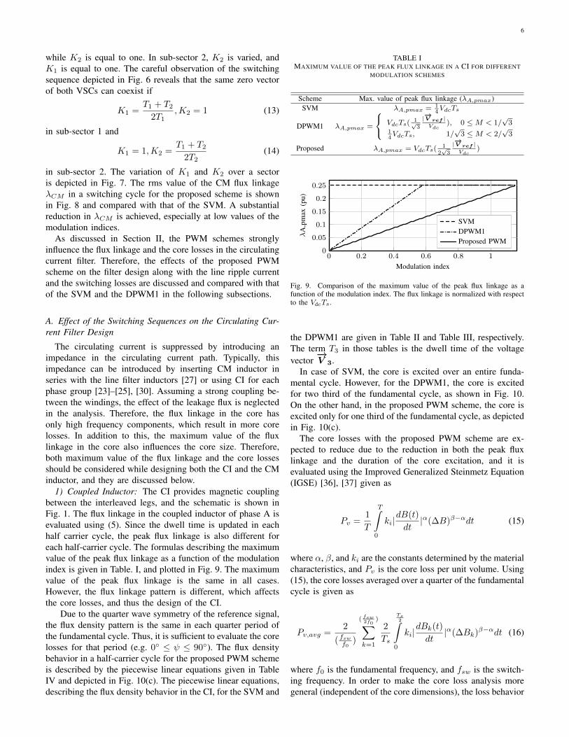
1) Coupled Inductor: The CI provides magnetic couplingbetween the interleaved legs, and the schematic is shown inFig. 1. The flux linkage in the coupled inductor of phase A isevaluated using (5). Since the dwell time is updated in eachhalf carrier cycle, the peak flux linkage is also different foreach half-carrier cycle. The formulas describing the maximumvalue of the peak flux linkage as a function of the modulationindex is given in Table. I, and plotted in Fig. 9. The maximumvalue of the peak flux linkage is the same in all cases.However, the flux linkage pattern is different, which affectsthe core losses, and thus the design of the CI.
Due to the quarter wave symmetry of the reference signal,the flux density pattern is the same in each quarter period ofthe fundamental cycle. Thus, it is sufficient to evaluate the corelosses for that period (e.g. 0 ≤ ψ ≤ 90). The flux densitybehavior in a half-carrier cycle for the proposed PWM schemeis described by the piecewise linear equations given in TableIV and depicted in Fig. 10(c). The piecewise linear equations,describing the flux density behavior in the CI, for the SVM and
TABLE IMAXIMUM VALUE OF THE PEAK FLUX LINKAGE IN A CI FOR DIFFERENT
MODULATION SCHEMES
Scheme Max. value of peak flux linkage (λA,pmax)SVM λA,pmax = 1
4VdcTs
DPWM1 λA,pmax =
VdcTs(1√3
|−→V ref |Vdc
), 0 ≤M < 1/√3
14VdcTs, 1/
√3 ≤M < 2/
√3
Proposed λA,pmax = VdcTs(1
2√3
|−→V ref |Vdc
)
0 0.2 0.4 0.6 0.8 10
0.1
0.2
0.05
0.15
0.25
Modulation index
λA
,pm
ax(p
u)
SVMDPWM1Proposed PWM
Fig. 9. Comparison of the maximum value of the peak flux linkage as afunction of the modulation index. The flux linkage is normalized with respectto the VdcTs.
the DPWM1 are given in Table II and Table III, respectively.The term T3 in those tables is the dwell time of the voltagevector
−→V 3.
In case of SVM, the core is excited over an entire funda-mental cycle. However, for the DPWM1, the core is excitedfor two third of the fundamental cycle, as shown in Fig. 10.On the other hand, in the proposed PWM scheme, the core isexcited only for one third of the fundamental cycle, as depictedin Fig. 10(c).
The core losses with the proposed PWM scheme are ex-pected to reduce due to the reduction in both the peak fluxlinkage and the duration of the core excitation, and it isevaluated using the Improved Generalized Steinmetz Equation(IGSE) [36], [37] given as
Pv =1
T
T∫0
ki|dB(t)
dt|α(∆B)β−αdt (15)
where α, β, and ki are the constants determined by the materialcharacteristics, and Pv is the core loss per unit volume. Using(15), the core losses averaged over a quarter of the fundamentalcycle is given as
Pv,avg =2
( fswf0 )
( fsw2f0
)∑k=1
2
Ts
Ts2∫
0
ki|dBk(t)
dt|α(∆Bk)β−αdt (16)
where f0 is the fundamental frequency, and fsw is the switch-ing frequency. In order to make the core loss analysis moregeneral (independent of the core dimensions), the loss behavior

7
TABLE IIFLUX DENSITY DESCRIPTION IN A HALF-CARRIER CYCLE USING PIECEWISE LINEAR EQUATIONS FOR SVM
PWM scheme Sub-sector Peak flux density Bp Flux density B(t)
SVM 0 ≤ ψ ≤ 90 Bp =Vdc(Tz)8NAc
B(t) =4Bp
Tzt for 0 ≤ t ≤ Tz
4
B(t) = Bp for Tz2≤ t ≤ (Ts
2− Tz
4)
B(t) = Bp −4Bp
Tz[t− (Ts
2− Tz
4)] for (Ts
2− Tz
4) ≤ t ≤ Ts
2
TABLE IIIDPWM1: FLUX DENSITY DESCRIPTION IN A HALF SWITCHING CYCLE USING PIECEWISE LINEAR EQUATIONS
Sub-sector−→V ref position Peak flux density Bp Flux density B(t)
0 ≤ ψ ≤ 30 - Bp = 0 B(t) = 0
30 ≤ ψ ≤ 60
M cos(30− ψ) > 1√3
Bp = VdcTz4NAc
B(t) =−2Bp
Tzt, for 0 ≤ t ≤ Tz
2
B(t) = −Bp, for Tz2≤ t ≤ Ts−Tz
2
B(t) = −Bp +2Bp
Tz[t− (Ts−Tz
2)], for Ts−Tz
2≤ t ≤ Ts
2
M cos(30− ψ) < 1√3
Bp =Vdc(T1+T2)
4NAc
B(t) =−2Bp
T1+T2t, for 0 ≤ t ≤ T1+T2
2
B(t) = −Bp, for T1+T22≤ t ≤ Ts−T1+T2
2
B(t) = −Bp +2Bp
T1+T2[t− (Ts−T1−T2
2)], for Ts−T1−T2
2≤ t ≤ Ts
2
60 ≤ ψ ≤ 90
M sin(60− ψs) > 1√3
Bp =Vdc(Tz+T3)
4NAc
B(t) =−2Bp
Tz+T3t, for 0 ≤ t ≤ Tz+T3
2
B(t) = −Bp, for Tz+T32≤ t ≤ Ts−Tz−T3
2
B(t) = −Bp +2Bp
Tz+T3[t− (Ts−Tz−T3
2)], for Ts−Tz−T3
2≤ t ≤ Ts
2
M sin(60− ψs) > 1√3
Bp = VdcT24NAc
B(t) =−2Bp
T2t, for 0 ≤ t ≤ T2
2
B(t) = −Bp, for T22≤ t ≤ Ts−T2
2
B(t) = −Bp +2Bp
Tz+T3[t− (Ts−T2
2)], for Ts−T2
2≤ t ≤ Ts
2
TABLE IVFLUX DENSITY DESCRIPTION IN CI FOR THE PROPOSED PWM SCHEME USING PIECEWISE LINEAR EQUATIONS
Sub-sector Peak flux density Bp Flux density B(t)0 ≤ ψ ≤ 60 Bp = 0 B(t) = 0
60 ≤ ψ ≤ 90 Bp =Vdc(T3)4NAc
B(t) =2Bp
T3t for 0 ≤ t ≤ T3
2
B(t) = Bp for T32≤ t ≤ Ts−T3
2
B(t) = Bp −2Bp
T3[t− (Ts−T3
2)] for Ts−T3
2≤ t ≤ Ts
2
is described in terms of Bmax and Ts, as
Pv,avg =2
( fswf0 )
( fsw2f0
)∑k=1
2
Ts
Ts2∫
0
ki(4Bmaxfsw)α(∆Bk)β−αdt
(17)To make the core losses comparison independent of the designparameters, the analysis is presented in terms of the CoreLoss Function (CLF), where CLF is given as the ratio of theaverage volumetric core loss for a PWM scheme to the averagevolumetric core loss for the SVM at a given modulation indexM .
CLF =Pv,avg(M)
Pv,avg(SVM)(M)(18)
The CLFs for all considered PWM schemes are depicted inFig. 11. Amorphous metal core is considered, where α = 1.51,β = 1.74, and ki = 0.622. Lower core losses over the entiremodulation range are observed for the proposed method com-pared to the other considered schemes. The use of the SVMresults in highest core losses in the CI for low modulationindices (M < 0.6), whereas the core losses are the highest incase of DPWM1 at high modulation indices.
The volume optimized design of the inductor often resultsin non-saturated thermally limited design, and the core lossesprimarily determine the size of the CI [38]. Due to the sub-stantial reduction in the core losses with the proposed scheme,small size of the CI with minimal thermal management canbe achieved with the proposed PWM scheme.
2) Common-mode Inductor: Asiminoaei et al. [27] pro-posed the use of a CM inductor to reduce the circulatingcurrent. This solution permits un-equal load sharing betweenthe parallel interleaved VSCs and scalability, and may be apreferred solution when the modularity is the main designobjective. The volume of the CM inductor can be minimizedby reducing either the maximum value of the peak CM fluxlinkage or the core losses. The maximum value of the peak CMflux linkage as a function of the modulation index is given inTable V and plotted in Fig. 12 for the proposed PWM schemealong with that of the SVM and the DPWM1.
For SVM, the maximum value of the peak flux linkageincreases as the modulation index decreases. Therefore, forapplications demanding operation over the full modulationrange, the CM inductor has to be designed for the maximumflux linkage, which occurs at low modulation indices. On the
8
TABLE VMAXIMUM VALUE OF THE PEAK CM FLUX LINKAGE
PWM scheme Max of the peak CM flux linkage (λCM,pmax)
SVM λCM,pmax = VdcTs(14− 1
3√3
|−→V ref |Vdc
)
DPWM1 λCM,pmax = VdcTs(13
|−→V ref |Vdc
) for (0 ≤ M≤ 23
)
λCM,pmax = VdcTs(
13− 1
3
|−→V ref |Vdc
cos(60− arcsin√
3Vdc
4|−→V ref |
))
for ( 23≤ M≤ 2√
3)
Proposed PWM scheme λCM,pmax = VdcTs(1
6√3
|−→V ref |Vdc
)
0 20 40 60 80−1
−0.5
0
0.5
1
Reference space vector angle ψ
B(T
)
M = 0.5
M = 1
(a)
0 20 40 60 80−1
−0.5
0
0.5
1
Reference space vector angle ψ
B(T
)
M = 0.5
M = 1
(b)
0 20 40 60 80−1
−0.5
0
0.5
1
Reference space vector angle ψ
B(T
)
M = 0.5
M = 1
(c)
Fig. 10. The flux density pattern in the CI core for modulation indices of 0.5and 1. (a) SVM, (b) DPWM1, (c) Proposed scheme.
0.2 0.4 0.6 0.8 10
0.5
1
1.15
0.25
0.75
1.25
Modulation index
CL
F
SVMDPWM1Proposed PWM
Fig. 11. CLF as a function of the modulation index.
0 0.2 0.4 0.6 0.8 10
0.1
0.2
0.05
0.15
0.25
Modulation index
λC
M,p
max
(pu)
SVMDPWM1Proposed PWM
Fig. 12. Comparison of the maximum values of the peak CM flux linkageas a function of the modulation index. The flux linkage is normalized withrespect to VdcTs.
other hand, the CM is subjected to maximum flux linkagefor a modulation index M = 2/3 if DPWM1 is employed.The proposed PWM scheme has the lowest peak flux linkage,compared to other PWM schemes, for the entire modulationrange. The reduction in the maximum flux linkage in caseof the CM filter is achieved by using the proposed DPWMscheme. As a result, small CM inductor can be realized.
B. Ripple Current Analysis
The line current ripple of the proposed PWM scheme is an-alyzed and compared with that of the SVM and the DPWM1.The reference vector is synthesized using the discrete vectors.Thus, at any given instant, an error between the applied voltagevector and the reference vector exists. The error voltagevectors for a given sampling instance are shown in Fig. 13(a).The time integral of the error vectors gives the harmonic fluxvector, which is proportional to the ripple current [5], [20],[21].
In the synchronously rotating reference frame, the instanta-neous error voltage vectors depicted in Fig. 13(a) are given as
−→V err,1 = [cosψ − Vref ]− j sinψ (19a)
−→V err,2 = [cos(60 − ψ)− Vref ] + j sin(60 − ψ)(19b)
−→V err,z = −Vref (19c)
In the proposed scheme, the time duration, for which an activevector is applied, is divided unequally, and the division of theactive vector follows the rule given by (13) and (14). For the

9
q-axis
d-axis
−→V 1(100)
−→V 2(110)
−→V ref
−→Verr,1
−→ Verr,2
−→V err
,z
ψ−→V 0(000)−→V 7(111)
(a)
d-axis
q-axis
d-axisd-axis
ψ = 4.28
ψ = 12.85
ψ = 21.42
(b)
Fig. 13. (a) The active and zero vectors to synthesize given reference vectorand corresponding error voltage vectors, (b) Harmonic flux vector trajectoryfor different values of reference vector angle ψ for 1012 sequence in sub-sector 1.
2 1 0 1 1 0 1 2
1 0 1 2 2 1 0 1VSC1
VSC2
d−axis
q−axis
Ts
K1T1
(1−K1)T1
VSC1 ResultantVSC2
VSC2 Resultant VSC1
Fig. 14. d-axis and q-axis ripple components of a harmonic flux vector over aswitching cycle for two parallel VSCs and their resultant with an interleavingangle of 180 and reference vector angle ψ = 12.8.
proposed PWM scheme, the harmonic flux vector is given as−→V err,1K1T1 = [cosψ − Vref ]K1T1 − jK1T1 sinψ(20a)−→V err,1(1−K1)T1 = [cosψ − Vref ](1−K1)T1
−j(1−K1)T1 sinψ (20b)−→V err,2T2 = [cos(60 − ψ)− Vref ]T2
+jT2 sin(60 − ψ) (20c)−→V err,zTz = −VrefTz (20d)
and it is plotted in Fig. 13(b) for different values of thereference space vector angles. The harmonic flux vector isdecomposed into d-axis and q-axis components, as shownin Fig. 14. The resultant vector for an interleaving angle of180 is also shown, and it is used to evaluate the ripplecurrent/harmonic content in the line current.
The normalized rms value of the line current ripple over ahalf-carrier cycle [14] for different modulation indices for theproposed PWM scheme is plotted in Fig. 15(c) as a function ofthe ψ. The variation in the rms value of the line current ripplefor SVM and DPWM1 are also shown in Fig. 15(a) and 15(b),respectively. The variation of the total rms value of the linecurrent ripple over the entire modulation range is also shownin Fig. 16. DPWM1 demonstrates better line current quality
10 20 30 40 500
0.01
0.02
0.03
Reference space vector angle ψ
RM
Slin
ecu
rren
tri
pple
(pu)
M = 0.25
M = 0.5
M = 0.75
M = 1
M = 1.15
(a)
10 20 30 40 500
0.01
0.02
Reference space vector angle ψ
RM
Slin
ecu
rren
tri
pple
(pu)
M = 0.25
M = 0.5
M = 0.75
M = 1
M = 1.15
(b)
10 20 30 40 500
0.02
0.04
0.01
0.03
Reference space vector angle ψ
RM
Slin
ecu
rren
tri
pple
(pu)
M = 0.25
M = 0.5
M = 0.75
M = 1
M = 1.15
(c)
Fig. 15. Space dependency of the rms value of the line current ripple(normalized) for different modulation indices. (a) SVM, (b) DPWM1, (c)Proposed scheme.
0 0.2 0.4 0.6 0.8 10
0.02
0.04
0.06
Modulation index
RM
Slin
ecu
rren
tri
pple
(pu)
SVMDPMW1Proposed PWM
Fig. 16. Total rms value of the line current ripple (normalized) as a functionof modulation index.
over an entire modulation range. The total rms value of the linecurrent ripple for the proposed PWM scheme closely matchesthat of the SVM. For SVM, the harmonic content for lowmodulation indices is slightly less compared to the proposedPWM scheme. On the other hand, the line current quality inthe case of the proposed PWM scheme is marginally better

10
−50 0 500
0.5
1
0.25
0.75
1.25
Displacement power factor angle φ (degree)
SLF
SVMDPWM1Proposed PWM
Fig. 17. Comparison of the switching losses.
than that of the SVM at higher modulation indices (M>0.9).
C. Semiconductor losses
Although one of the phase legs is clamped to dc-link forone third period of the fundamental cycle in the proposedscheme, an additional commutation is introduced in anotherleg as explained in the previous section. Thus, the switchinglosses are also evaluated in this paper. The switching lossfunction (SLF) [18] is used to compare the switching lossesof the proposed PWM with other PWM schemes. The turn-onand turn-off characteristics of the semiconductor devices areassumed to be linear with respect to time. The contributionof the ripple current towards the switching losses is alsoneglected. Since the SLF normalizes the switching loss of theproposed method with respect to the switching loss of SVM,the relative error is small despite the simplified loss model[18] used. The SLF for the proposed method is given as
SLF =
1 + ( 2−
√3
2 ) cosφ, 0 6 |φ| < π6
cosφ+ 12 sinφ, π
6 6 |φ| < π3
2− ( 2√3−12 ) sinφ, π
3 6 |φ| 6 π2
(21)
where φ is the displacement power factor angle. The SLFsfor the proposed PWM scheme along with that of the SVMand DPWM1 are plotted in Fig. 17. For the unity power factorapplications, the switching losses are minimum if DPWM1 isused. For a displacement power factor angle higher than 53,the proposed method has lower switching losses comparedto that of the SVM. However, for a displacement powerfactor angle in the vicinity of zero, the proposed method hashigh switching losses. For the reactive power compensationapplications, the use of the proposed PWM scheme results inthe lowest switching losses, as shown in Fig. 17.
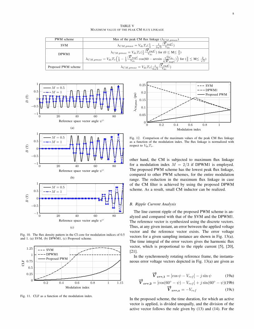
V. EXPERIMENTAL RESULTS
The experiments have been performed using single-phaseinductors, which act as both line filter inductor and thecirculating current filter. This arrangement is used to simplifythe measurement [39]. The results for IA1− IA2 are obtained,which is equal to 2×IA,c. As explained in Section II, the IA,cis proportional to the flux linkage in CI. Similarly, the sum ofthree-phase currents of each VSC is obtained. This current isequal to 3×ICM , and it is proportional to the CM flux linkage.The dc-link voltage of 600 V is used. The carrier frequency is
(a)
(b)
(c)
Fig. 18. The performance comparison of the proposed PWM scheme. Themodulation index M=0.3. Ch1: Phase A line current (5 A/div), Ch2: Phase Acirculating current (2 × IA,c) (5 A/div), Ch3: CM circulating current (3 ×ICM ) (5 A/div). (a) SVM, (b) DPWM1, (c) Proposed scheme.
taken to be 2.5 kHz and interleaving angle of 180is chosen.The line filter inductor of 6.8 mH is used, and a resistive loadis set to 20 Ω. The inductance in the circulating current pathis Lc = 2×6.8 mH.
The line current of phase A (IA), the circulating currentof Phase A (2×IA,c), and the CM current (3×ICM ) formodulation index of 0.3, 0.6, and 1 for SVM, DPWM1, andthe proposed PWM scheme is depicted in Fig. 18, 19, and20, respectively. The experiments have been performed forthe entire linear range of the modulation index and the resultsare given in Table VI. The line current THD, the maximumvalue of the peak circulating current of phase A, and themaximum value of the peak CM circulating current of theproposed method are compared with that of the SVM andthe DPWM1. The THD is calculated by performing discreteFourier transform of the measured line current.
For the SVM, the maximum value of the peak circulatingcurrent of phase A remains almost constant over the entiremodulation range. Since, the phase A circulating current is
11
TABLE VIPERFORMANCE COMPARISON OF THE PROPOSED METHOD
M Max. of IA,c (A) Max. of ICM (A) Line current THD (%)SVM DPWM1 Proposed SVM DPWM1 Proposed SVM DPWM1 Proposed
0.1 3.55 0.79 0.59 3.98 0.52 0.32 24.15 26.14 28.620.2 3.52 1.46 0.85 3.12 0.93 0.33 22.30 19.29 25.310.3 3.50 2.09 1.15 2.89 1.28 0.46 19.60 15.21 22.060.4 3.55 2.68 1.42 2.71 1.62 0.52 17.63 11.56 19.680.5 3.50 3.23 1.76 2.57 1.94 0.61 15.86 7.95 16.490.6 3.48 3.72 2.03 2.38 2.27 0.73 13.85 6.03 14.380.7 3.48 3.63 2.28 2.20 2.39 0.82 11.88 5.92 12.380.8 3.42 3.55 2.53 2.03 2.10 0.91 10.03 5.85 10.260.9 3.40 3.50 2.81 1.85 1.86 0.98 8.25 5.28 8.091.0 3.40 3.48 3.03 1.64 1.64 1.14 6.37 4.49 6.171.1 3.36 3.48 3.19 1.46 1.49 1.27 4.71 3.66 4.471.15 3.38 3.39 3.37 1.39 1.28 1.29 4.05 3.31 3.87
(a)
(b)
(c)
Fig. 19. The performance comparison of the proposed PWM scheme. Themodulation index M=0.6. Ch1: Phase A line current (10 A/div), Ch2: PhaseA circulating current (2× IA,c) (5 A/div), Ch3: CM circulating current (3×ICM ) (5 A/div). (a) SVM, (b) DPWM1, (c) Proposed scheme.
proportional to the flux linkage in the CI, it can be concludedthat the maximum value of peak flux linkage in the CI over thefull modulation range also remains constant. The use of SVMalso results in more core losses in case of CI compared to theproposed PWM scheme, as the core is excited over the entire
(a)
(b)
(c)
Fig. 20. The performance comparison of the proposed PWM scheme. Themodulation index M=1. (a) SVM: Ch1: Phase A line current (10 A/div), Ch2:Phase A circulating current (2×IA,c) (5 A/div), Ch3: CM circulating current(3× ICM ) (5 A/div), (b) DPWM1, (c) Proposed scheme.
fundamental cycle. The ICM is proportional to the flux linkagein the CM inductor and the experimental results of ICM arealso obtained. For the SVM, the maximum value of the peakCM circulating current decreases with the increase in themodulation index, which is in agreement with the analytical

12
100 200 300 400 500
10−3
10−2
10−1
100
Harmonic order
Har
mon
icm
agni
tude
(pu)
Fig. 21. Proposed scheme: Experimental line current harmonic spectrumfor a modulation index of 1. The harmonic magnitude is normalized to themagnitude of the fundamental component.
result presented in Section IV and illustrated in Fig. 12. Inthe proposed scheme, the maximum value of the ICM occursat full modulation index, and it decreases with decrease inthe modulation index. The maximum value of the peak CMcurrent is 1.29 A at a modulation index of one in the proposedscheme, compared to 3.98 A at modulation index of 0.1 incase of the SVM and 2.39 A at a modulation index of 0.7for DPWM1. Thus, for applications demanding the operationover the full modulation range, the use of the proposed PWMscheme results in size reduction of CM inductor.
The undesirable effect of larger duration of Tz at lowermodulation indices can be reduced by the same zero vectoralignment in the proposed scheme. In case of CI, the core isexcited only for the one third period of the fundamental cycle,as evident from the waveform of the IA,c in experimentalresults. If the design of CI is thermally limited, the reducedcore losses result in more compact design. The harmonicanalysis of the line current is shown in Fig. 21. The majorharmonic components are pushed close to the double of theswitching frequency by the interleaving effect.
VI. CONCLUSION
A PWM scheme to reduce the maximum value of the fluxlinkage and the core losses in the circulating current filter ispresented in this paper. This PWM scheme uses the divisionof the active vectors within a half-carrier cycle to ensuresimultaneous occurrence of the same zero vector in both of theVSCs. The effect of the proposed PWM scheme on the fluxlinkage and the core losses in the circulating current filter isanalyzed. Both the maximum value of the flux linkage and thecore losses are reduced substantially by the same zero vectoralignment in the proposed PWM scheme. Thus, the size ofthe circulating current filter can be reduced. The switchinglosses are also analyzed for the proposed PWM scheme andcompared with that of the SVM and 60clamped DPWM.The proposed PWM scheme demonstrates superior efficiencyfor the reactive power compensation applications, as it isevident from the core losses and switching losses comparisonspresented in this paper. However, for the applications, wherethe displacement power factor angle is in the vicinity ofzero, the use of proposed method results in high switching
losses. The line current ripple for the proposed scheme is alsoanalyzed, which shows that the THD of the line current closelymatches that of the SVM. The line current quality is superior inthe case of the DPWM1, however the improvement is marginalat the higher modulation indices. The PWM scheme and theanalysis presented in this paper are also supported by theexperimental results.
REFERENCES
[1] M. Baumann and J. Kolar, “Parallel connection of two three-phasethree-switch buck-type unity-power-factor rectifier systems with dc-linkcurrent balancing,” IEEE Trans. Ind. Electron., vol. 54, no. 6, pp. 3042–3053, 2007.
[2] Z. Xu, R. Li, H. Zhu, D. Xu, and C. Zhang, “Control of parallel multipleconverters for direct-drive permanent-magnet wind power generationsystems,” IEEE Trans. Power Electron., vol. 27, no. 3, pp. 1259–1270,March 2012.
[3] “Technical guidline: Generating plants connected to the medium-voltagenetwork.” BDEW Bundesverband der Energie- und Wasserwirtschafte.V., [Online]. Available: http://www.bdew.de, 2008.
[4] A. Rockhill, M. Liserre, R. Teodorescu, and P. Rodriguez, “Grid-filterdesign for a multimegawatt medium-voltage voltage-source inverter,”IEEE Trans. Ind. Electron., vol. 58, no. 4, pp. 1205–1217, 2011.
[5] G. Narayanan, V. T. Ranganathan, D. Zhao, H. Krishnamurthy, andR. Ayyanar, “Space vector based hybrid pwm techniques for reducedcurrent ripple,” IEEE Trans. Ind. Electron., vol. 55, no. 4, pp. 1614–1627, 2008.
[6] D. Casadei, G. Serra, A. Tani, and L. Zarri, “Theoretical and exper-imental analysis for the rms current ripple minimization in inductionmotor drives controlled by svm technique,” IEEE Trans. Ind. Electron.,vol. 51, no. 5, pp. 1056–1065, Oct 2004.
[7] M. Meco-Gutierrez, F. Perez-Hidalgo, F. Vargas-Merino, and J. R.Heredia-Larrubia, “A new pwm technique frequency regulated carrierfor induction motors supply,” IEEE Trans. Ind. Electron., vol. 53, no. 5,pp. 1750–1754, Oct 2006.
[8] K. Taniguchi, M. Inoue, Y. Takeda, and S. Morimoto, “A pwm strategyfor reducing torque-ripple in inverter-fed induction motor,” IEEE Trans.Ind. Appl., vol. 30, no. 1, pp. 71–77, Jan 1994.
[9] J. Prasad and G. Narayanan, “Minimization of Grid Current Distortionin Parallel-Connected Converters Through Carrier Interleaving,” IEEETrans. Ind. Electron., vol. 1, no. c, pp. 1–1, 2013.
[10] S. Miller, T. Beechner, and J. Sun, “A comprehensive study of harmoniccancellation effects in interleaved three-phase vscs,” in Proc. IEEEPower Electronics Specialists Conference, 2007. PESC 2007., 2007, pp.29–35.
[11] L. Asimmoaei, E. Aeloiza, J. Kim, P. Enjeti, F. Blaabjerg, L. Moran,and S. Sul, “An interleaved active power filter with reduced size ofpassive components,” in Proc. Twenty-First Annual IEEE Applied PowerElectronics Conference and Exposition, 2006. APEC ’06., 2006, pp. 1–7.
[12] D. Zhang, F. Wang, R. Burgos, L. Rixin, and D. Boroyevich, “Impactof Interleaving on AC Passive Components of Paralleled Three-PhaseVoltage-Source Converters,” IEEE Trans. Power Electron., vol. 46, no. 3,pp. 1042–1054, 2010.
[13] T. Bhavsar and G. Narayanan, “Harmonic analysis of advanced bus-clamping pwm techniques,” IEEE Trans. Power Electron., vol. 24,no. 10, pp. 2347–2352, 2009.
[14] X. Mao, A. Jain, and R. Ayyanar, “Hybrid interleaved space vectorpwm for ripple reduction in modular converters,” IEEE Trans. PowerElectron., vol. 26, no. 7, pp. 1954–1967, 2011.
[15] M. Abusara and S. Sharkh, “Design and control of a grid-connectedinterleaved inverter,” IEEE Trans. Power Electron., vol. 28, no. 2, pp.748–764, Feb 2013.
[16] K. Xing, F. Lee, D. Borojevic, Z. Ye, and S. Mazumder, “Interleavedpwm with discontinuous space-vector modulation,” IEEE Trans. PowerElectron., vol. 14, no. 5, pp. 906–917, 1999.
[17] D. G. Holmes and T. A. Lipo, Pulse Width Modulation for PowerConverters: Principles and Practice. Hoboken, NJ: Wiley-IEEE Press,2003.
[18] A. Hava, R. Kerkman, and T. Lipo, “Simple analytical and graphicalmethods for carrier-based pwm-vsi drives,” IEEE Trans. Power Elec-tron., vol. 14, no. 1, pp. 49–61, Jan 1999.
[19] J. Kolar, H. Ertl, and F. C. Zach, “Influence of the modulation methodon the conduction and switching losses of a pwm converter system,”IEEE Trans. Ind. Appl., vol. 27, no. 6, pp. 1063–1075, 1991.
13
[20] G. Narayanan and V. T. Ranganathan, “Analytical evaluation of harmonicdistortion in pwm ac drives using the notion of stator flux ripple,” IEEETrans. Power Electron., vol. 20, no. 2, pp. 466–474, 2005.
[21] G. Narayanan, H. Krishnamurthy, D. Zhao, and R. Ayyanar, “Advancedbus-clamping pwm techniquesbased on space vector approach,” IEEETrans. Power Electron., vol. 21, no. 4, pp. 974–984, 2006.
[22] H. Akagi, A. Nabae, and S. Atoh, “Control strategy of active powerfilters using multiple voltage-source pwm converters,” IEEE Trans. Ind.Appl., vol. IA-22, no. 3, pp. 460–465, 1986.
[23] R. Hausmann and I. Barbi, “Three-phase multilevel bidirectional dc-acconverter using three-phase coupled inductors,” in Proc. IEEE EnergyConversion Congress and Exposition, 2009. ECCE 2009., Sept 2009,pp. 2160–2167.
[24] F. Forest, E. Laboure, T. Meynard, and V. Smet, “Design and comparisonof inductors and intercell transformers for filtering of pwm inverteroutput,” IEEE Trans. Power Electron., vol. 24, no. 3, pp. 812–821, 2009.
[25] B. Cougo, T. Meynard, and G. Gateau, “Parallel Three-Phase Inverters:Optimal PWM Method for Flux Reduction in Intercell Transformers,”IEEE Trans. Power Electron., vol. 26, no. 8, pp. 2184–2191, Aug. 2011.
[26] B. Cougo, G. Gateau, T. Meynard, M. Bobrowska-Rafal, andM. Cousineau, “PD modulation scheme for three-phase parallel multi-level inverters,” IEEE Trans. Ind. Electron., vol. 59, no. 2, pp. 690–700,2012.
[27] L. Asiminoaei, E. Aeloiza, P. N. Enjeti, and F. Blaabjerg, “Shunt active-power-filter topology based on parallel interleaved inverters,” IEEETrans. Ind. Electron., vol. 55, no. 3, pp. 1175–1189, 2008.
[28] J. Ewanchuk, S. Member, and J. Salmon, “Three-limb Coupled InductorOperation for Voltage Sourced Inverters,” IEEETrans. on Ind. Electron.,vol. 60, no. 5, pp. 1979–1988, 2013.
[29] D. Zhang, F. Wang, R. Burgos, and D. Boroyevich, “Common-modecirculating current control of paralleled interleaved three-phase two-levelvoltage-source converters with discontinuous space-vector modulation,”IEEE Trans. Power Electron., vol. 26, no. 12, pp. 3925–3935, Dec 2011.
[30] D. Zhang, F. Wang, R. Burgos, and D. Boroyvich, “Total flux min-imization control for integrated inter-phase inductors in paralleled,interleaved three-phase two-level voltage-source converters with discon-tinuous space-vector modulation,” IEEE Trans. Power Electron., vol. 27,no. 4, pp. 1679–1688, April 2012.
[31] F. Luo, S. Wang, F. Wang, D. Boroyevich, N. Gazel, Y. Kang, andA. Baisden, “Analysis of cm volt-second influence on cm inductorsaturation and design for input emi filters in three-phase dc-fed motordrive systems,” IEEE Trans. Power Electron., vol. 25, no. 7, pp. 1905–1914, 2010.
[32] V. Blasko and V. Kaura, “A novel control to actively damp resonancein input lc filter of a three-phase voltage source converter,” IEEE Trans.Ind. Appl., vol. 33, no. 2, pp. 542–550, Mar 1997.
[33] A. Hava, R. Kerkman, and T. Lipo, “A high-performance generalizeddiscontinuous pwm algorithm,” IEEE Trans. Ind. Appl., vol. 34, no. 5,pp. 1059–1071, 1998.
[34] H. Krishnamurthy, G. Narayanan, R. Ayyanar, and V. T. Ranganathan,“Design of space vector-based hybrid pwm techniques for reduced cur-rent ripple,” in Proc. Eighteenth Annual IEEE Applied Power ElectronicsConference and Exposition, 2003. APEC ’03., vol. 1, 2003, pp. 583–588.
[35] A. C. Binojkumar, J. Prasad, and G. Narayanan, “Experimental inves-tigation on the effect of advanced bus-clamping pulsewidth modulationon motor acoustic noise,” IEEE Trans. Ind. Electron., vol. 60, no. 2, pp.433–439, Feb 2013.
[36] K. Venkatachalam, C. Sullivan, T. Abdallah, and H. Tacca, “Accurateprediction of ferrite core loss with nonsinusoidal waveforms usingonly steinmetz parameters,” in Computers in Power Electronics, 2002.Proceedings. 2002 IEEE Workshop on, 2002, pp. 36–41.
[37] J. Li, T. Abdallah, and C. Sullivan, “Improved calculation of core losswith nonsinusoidal waveforms,” in Industry Applications Conference,2001. Thirty-Sixth IAS Annual Meeting. Conference Record of the 2001IEEE, vol. 4, 2001, pp. 2203–2210 vol.4.
[38] A. V. d. Bossche and V. C. Valchev, Inductors and Transformers forPower Electronics. Boca Raton, FL: CRC Press, 2004.
[39] B. Cougo, T. Meynard, and G. Gateau, “Parallel three-phase inverters:Optimal pwm method for flux reduction in intercell transformers,” IEEETrans. Power Electron., vol. 26, no. 8, pp. 2184–2191, Aug 2011.
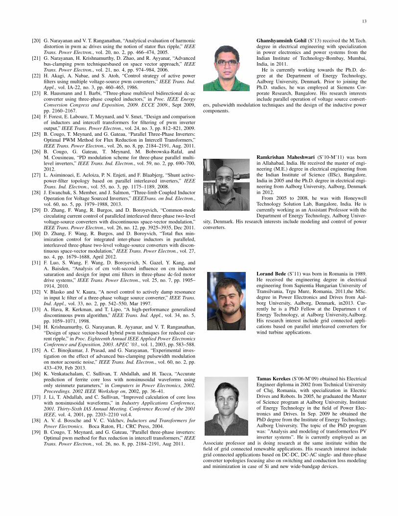
Ghanshyamsinh Gohil (S’13) received the M.Tech.degree in electrical engineering with specializationin power electronics and power systems from theIndian Institute of Technology-Bombay, Mumbai,India, in 2011.
He is currently working towards the Ph.D. de-gree at the Department of Energy Technology,Aalborg University, Denmark. Prior to joining thePh.D. studies, he was employed at Siemens Cor-porate Research, Bangalore. His research interestsinclude parallel operation of voltage source convert-
ers, pulsewidth modulation techniques and the design of the inductive powercomponents.
Ramkrishan Maheshwari (S’10-M’11) was bornin Allahabad, India. He received the master of engi-neering (M.E.) degree in electrical engineering fromthe Indian Institute of Science (IISc), Bangalore,India in 2005 and the Ph.D. degree in electrical engi-neering from Aalborg University, Aalborg, Denmarkin 2012.
From 2005 to 2008, he was with HoneywellTechnology Solution Lab, Bangalore, India. He iscurrently working as an Assistant Professor with theDepartment of Energy Technology, Aalborg Univer-
sity, Denmark. His research interests include modeling and control of powerconverters.
Lorand Bede (S’11) was born in Romania in 1989.He received the engineering degree in electricalengineering from Sapientia Hungarian University ofTransilvania, Trgu Mure, Romania, 2011,the MSc.degree in Power Electronics and Drives from Aal-borg University, Aalborg, Denmark, in2013. Cur-rently he is a PhD Fellow at the Departmen t ofEnergy Technology, at Aalborg University,Aalborg.His research interest include grid connected appli-cations based on parallel interleaved converters forwind turbine applications.
Tamas Kerekes (S’06-M’09) obtained his ElectricalEngineer diploma in 2002 from Technical Universityof Cluj, Romania, with specialization in ElectricDrives and Robots. In 2005, he graduated the Masterof Science program at Aalborg University, Instituteof Energy Technology in the field of Power Elec-tronics and Drives. In Sep. 2009 he obtained thePhD degree from the Institute of Energy Technology,Aalborg University. The topic of the PhD programwas: ”Analysis and modeling of transformerless PVinverter systems”. He is currently employed as an
Associate professor and is doing research at the same institute within thefield of grid connected renewable applications. His research interest includegrid connected applications based on DC-DC, DC-AC single- and three-phaseconverter topologies focusing also on switching and conduction loss modelingand minimization in case of Si and new wide-bandgap devices.

14
Remus Teodorescu (S’94-A’97-M’99-SM’02-F’12)received the Dipl.Ing. degree in electrical engineer-ing from Polytechnical University of Bucharest, Ro-mania in 1989, and PhD. degree in power electronicsfrom University of Galati, Romania, in 1994. In1998, he joined Aalborg University, Department ofEnergy Technology, power electronics section wherehe currently works as full professor. Since 2013he is a visiting professor at Chalmers University.He has coauthored the book Grid Converters forPhotovoltaic and Wind Power Systems, ISBN: 978-
0-470-05751-3, Wiley 2011 and over 200 IEEE journals and conferencepapers. His areas of interests includes: design and control of grid-connectedconverters for photovoltaic and wind power systems, HVDC/FACTS basedon MMC, SiC-based converters, storage systems for utility based on Li-Ionbattery technology. He was the coordinator of the Vestas Power Program 20082013.
Marco Liserre (S’00-M’02-SM’07-F’13) receivedthe MSc and PhD degree in Electrical Engineeringfrom the Bari Polytechnic, respectively in 1998 and2002. He has been Associate Professor at Bari Poly-technic and Professor in reliable power electronicsat Aalborg University (Denmark). He is currentlyFull Professor and he holds the Chair of PowerElectronics at Christian-Albrechts-University of Kiel(Germany). He has published 200 technical papers(56 of them in international peer-reviewed journals),3 chapters of a book and a book (Grid Converters
for Photovoltaic and Wind Power Systems, ISBN-10: 0-470-05751-3 IEEE-Wiley, second reprint, also translated in Chinese). These works have receivedmore than 9000 citations. Marco Liserre is listed in ISI Thomson report Theworlds most influential scientific minds, 2014.
He has been recently awarded with an ERC Consolidator Grant for anoverall budget of 2 MEuro for the project The Highly Efficient And Reliablesmart Transformer (HEART), a new Heart for the Electric Distribution System.
He is member of IAS, PELS, PES and IES. He is Associate Editor of theIEEE Transactions on Industrial Electronics, IEEE Industrial Electronics Mag-azine, IEEE Transactions on Industrial Informatics, where he is currently Co-Eic, IEEE Transactions on power electronics and IEEE Journal of Emergingand Selected Topics in Power Electronics. He has been Founder and Editor-in-Chief of the IEEE Industrial Electronics Magazine, Founder and the Chairmanof the Technical Committee on Renewable Energy Systems, Co-Chairmanof the International Symposium on Industrial Electronics (ISIE 2010), IESVice-President responsible of the publications. He has received the IES 2009Early Career Award, the IES 2011 Anthony J. Hornfeck Service Award, the2014 Dr. Bimal Bose Energy Systems Award, the 2011 Industrial ElectronicsMagazine best paper award and the Third Prize paper award by the IndustrialPower Converter Committee at ECCE 2012, 2012. He is senior member ofIES AdCom. In 2013 he has been elevated to the IEEE fellow grade with thefollowing citation for contributions to grid connection of renewable energysystems and industrial drives.
Frede Blaabjerg (S’86-M’88-SM’97-F’03) waswith ABB-Scandia, Randers, Denmark, from 1987to 1988. From 1988 to 1992, he was a Ph.D. Studentwith Aalborg University, Aalborg, Denmark. Hebecame an Assistant Professor in 1992, an Asso-ciate Professor in 1996, and a Full Professor ofpower electronics and drives in 1998. His currentresearch interests include power electronics and itsapplications such as in wind turbines, PV systems,reliability, harmonics and adjustable speed drives.
He has received 15 IEEE Prize Paper Awards, theIEEE PELS Distinguished Service Award in 2009, the EPE-PEMC CouncilAward in 2010, the IEEE William E. Newell Power Electronics Award 2014and the Villum Kann Rasmussen Research Award 2014. He was an Editor-in-Chief of the IEEE TRANSACTIONS ON POWER ELECTRONICS from2006 to 2012. He has been Distinguished Lecturer for the IEEE PowerElectronics Society from 2005 to 2007 and for the IEEE Industry ApplicationsSociety from 2010 to 2011.
![High-order Runge-Kutta discontinuous Galerkin methods with a … · new modified version of the original KXRCF indicator [24], to build a sequence of hierar- ... DG solution. The](https://img.pdfslide.us/doc/110x75/5fb4611dfc722e65b07078c1/high-order-runge-kutta-discontinuous-galerkin-methods-with-a-new-modiied-version.jpg)