Embed Size (px)
Citation preview
EQUIPMENT CONTROL AND COMPUTER
INTERFACING USING LabVIEW
by
MUHIUZZAMAN MAHMUD, B.S.E.
A THESIS
IN
ELECTRICAL ENGINEERING
Submitted to the Graduate Faculty of Texas Tech University in
Partial Fulfillment of the Requirements for
the Degree of
MASTER OF SCIENCE
IN
ELECTRICAL ENGINEERING
Approved
Accepted
May, 2000

ACKNOWLEDGEMENTS
I am extremely grateful to Dr. Henryk Temkin, Professor and Maddox Chair,
Department of Electrical Engineering, Texas Tech University. He gave me the
opportunity to work in the two exciting projects that form the subject of this thesis. Apart
from the very helpful guidance and advice regarding research work, his professionalism
and sheer dedication to work will always inspire me. I am also very thankful to Dr.
Sunanda Mitra, Professor and Director of C VIAL, Department of Electrical Engineering,
Texas Tech University for providing good advice and sincere encouragement that led to
this thesis. In spite of her busy schedule. Dr. Mitra always was there when I needed
research direction. Many thanks to Dr. Micheal E. Parten, Professor, Department of
Electrical Engineering for his time and advice as a member of my thesis committee.
Special thanks to Ms. Barbi Dickensheet of the Graduate School for her invaluable help.
Last but not the least, thanks to my wife Nahid and our newborn daughter Parisa
who are a constant source of motivation for me. They make it all worthwhile.
11
CONTENTS
ACKNOWLEDGEMENTS ii
LIST OF TABLES v
LIST OF FIGURES vi
CHAPTER
1. INTRODUCTION 1
2. DIGITAL DATA ACQUISITION
FROM ACCDCHIP(TC211 ) 4
2.1 Overall System Description 4
2.2 The Hardware Interface 5
2.3. The Control Software 9
2.4 The Component vi Descriptions 17
3 CONTROL OF A MAGNETRON
SPUTTERING EQUIPMENT 30
3.1 System Description And Control Flow 30
3.2 The Sub-Systems & Hardware Set-Up 32
3.3 The Software 33
3.4 The Component vi Descriptions 37
4 SUMMARY 49
4.1 Data Acquisition From CCD 49 4.2 Sputtering Equipment Control System 51
REFERENCES 52
111
APPENDIX
A. PIN CONNECTION AND SIGNAL FOR THE CCD DATA ACQUISITION PROJECT 53
B. THE SPUTTERING EQUIPMENT CONTROL 56
IV
LIST OF TABLES
A. 1 Pin correspondence between D25 connector of the interface board
and the DAQ card connector 54
A.2 Nibble selection and corresponding MUX enables 55
A.3 Input Bit Designations 55
B.l ASCII Command Syntax of Series 307 VGC 57
LIST OF FIGURES
2.1 Data flow schematic for the CCD imaging system 5
2.2 Schematic of the interface card 6
2.3 The GUI for the control software 9
2.4 Main program block before integration 10
2.5 Main program block during integration 12
2.6 Full-frame read-out 13
2.7 Data conversion 13
2.8 Single row read-out 14
2.9 Dummy pixel shift out 14
2.10 Single row read-out vi 14
2.11 Dark pixel shift out 15
2.12 Single row data conversion 15
2.13 After completion of the current imaging operation 16
2.14 srgpulse.vi diagram 17
2.15 lineshift.vi diagram 18
2.16 integration.vi, 210 SRG pulses generated 19
2.17 integration.vi, compares the time elapsed between vi start time and current time with the "integration time " input 20
2.18 MUX select bits (here output pattern is 3, i.e., 0011) are generated at Digital port B 21
2.19 4-bit Data read-in from Digital port A 22
VI
2.20 At start of fuUframereadout.vi the read-out register is cleared with 210
SRG Pulses 23
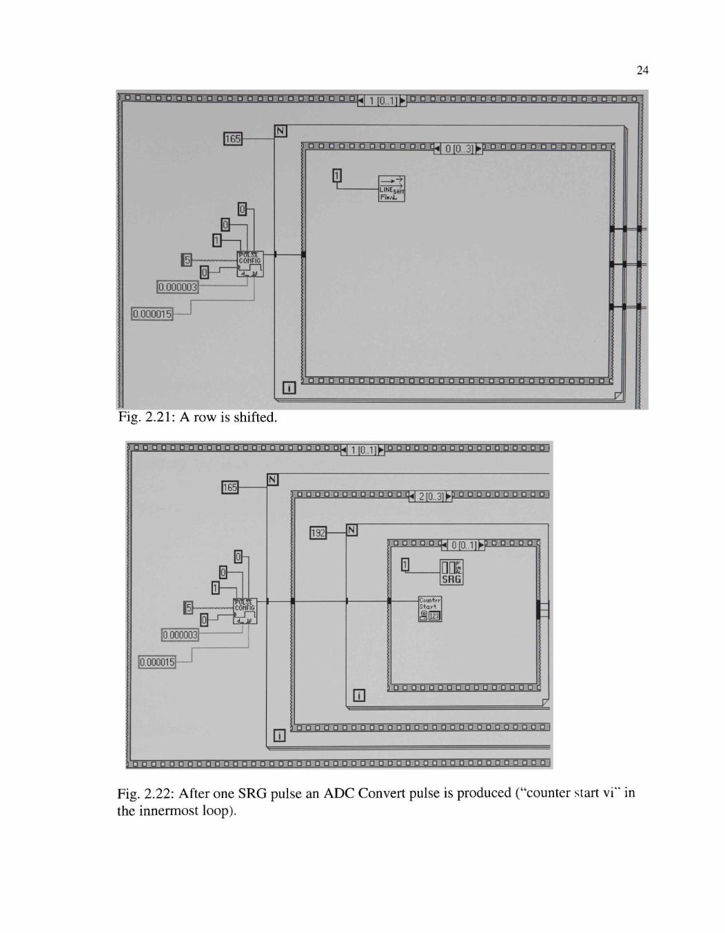
2.21 A row is shifted 24
2.22 After one SRG pulse an ADC Convert pulse is produced ("counter start vi"
in innermost loop) 24
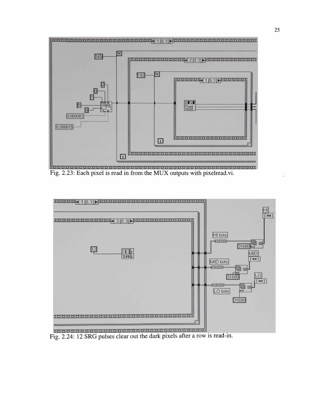
2.23 Each pixel is read in from the MUX outputs with pixelread.vi 25
2.24 12 SRG pulses clear out the dark pixels after a row is read-in 25
2.25 Each nibble is shifted appropriate number of places and then concatenated ... 27
2.26 singlerow_readout.vi diagram 28
2.27 single row data conversion diagram 29
3.1 System Control topology for the Endura® HP PVD system 31
3.2 The Main Control Panel 34
3.3 Accessing (a) Login prompt, (b) Login match found, (c) not found 35
3.4 The VGC control sub-menu 36
3.5 The default state for the main control vi 38
3.6 The Login state for the main control vi 39
3.7 VGC control is being accessed 39
3.8 Cryo-control panel being accessed 40
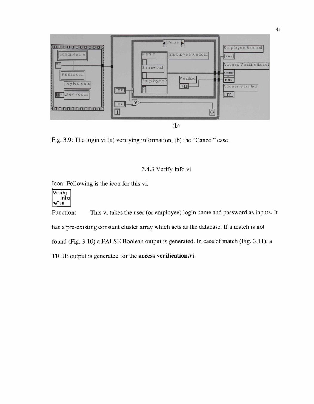
3.9 The login vi (a) verifying information, (b)the "Cancel" case 41
3.10 Verify info vi matches input to a existing database 42
3.11 Match found in database, login name verified 42 3.12 Access (a) denied and (b) granted 43
3.13 VGC controller vi 45
3.14 VGC controller vi, receiving Ion and Convectron gauge readings 46
vii
3.15 vgcwrite.vi (a) when talking and (b) idle 47
3.16 vgcread.vi (a) when listening and (b) idle 48
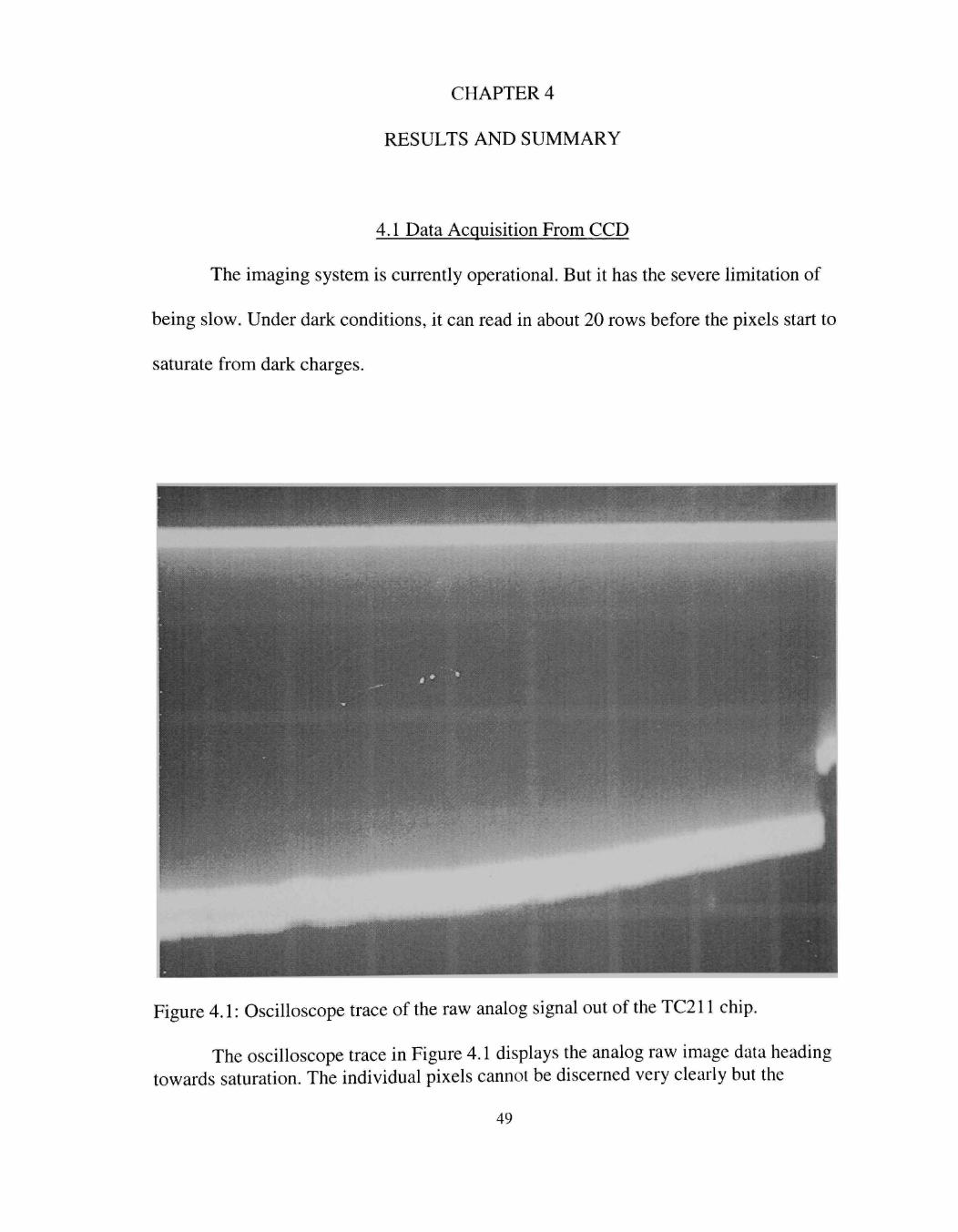
4.1 Oscilloscope trace of the raw analog signal out of the TC211 chip 49
4.2 The spreadsheet data showing saturation 50
Vl l l
CHAPTER 1
INTRODUCTION
This thesis describes two control projects undertaken at the Maddox Laboratory
of the Texas Tech University. The first project concerns digital image data acquisition
from a CCD chip into a PC. The second project deals with the control of a Magnetron
Sputtering equipment and its accessories. Both the projects culminate to working
LabVIEW programs that automate the controls for both the systems.
CCD sensors can be classified broadly into two categories - the linear sensors and
the area sensors. The sensor used in the data acquisition project was an area sensor of the
"full-frame" type. A matrix of photo-sensitive CCD pixels generate electron packets of
varying charge content that is proportional to the amount of incident photons. After a
finite integration period, during which photo-generated electronic charges accumulate
within the potential well of each CCD photo-site, the whole field of pixels is shifted
towards the output node. This shift towards the output node occurs in several steps. First,
a Vertical shift clock pulse causes all the rows to be shifted downwards by one position -
resulting into the bottom row being shifted to a serial shift register. A series of,
Horizontal-Shift clock pulses then shift out the pixels one by one through the shift
register into the output diffusion node. The output diffusion is voltage modulated by the
charge content in a pixel. This voltage is sensed by an output buffer amplifier. After all
the pixels in a row have been shifted out to the floating diffusion at the output and sensed
by the output amplifier, a row shift occurs again and the same sequence is repeated.
Once all the pixels have been shifted out and voltage levels have been buffered
and stored, voltage levels can be assigned corresponding gray-scale values and when the
gray values are arranged in the same order as the original pixels - an image is produced.
In this project, the raw analog output (voltages) from the CCD chip pass through a 12-bit
A-to-D converter and then fed into a DAQ card that has been used as the hardware
interface for LabVIEW. Some read-out electronics have been added in between the CCD
chip and the DAQ card. This accomplishes the digitization along with appropriate level
shifts and inversion of signals. The digitized signal is MUXed in to the DAQ card as 4-bit
nibbles. They are then concatenated and then converted back to analog values within the
software.
The LabVIEW program accepts a file name as a user input and uses the file to
store the voltage matrix in a spreadsheet format. So, the end result is a matrix of analog
values that range from 0 to 2.0E+12. This creates a matrix of twelve-bit-precision values.
Though it has not been done in this project, it is straightforward to translate the numbers
to a gray scale that will result in a discernible image.
The second project deals with the control system for a sputtering machine. A
variety of hardware interfaces are involved due to having different communication
protocol for different peripherals. The infrastructure for this fully independent automated
control system has been developed and parts of it have been implemented. The whole
control system has been divided into several sub-systems.
The user interface has been built with the idea that this expensive and complex
equipment will be operated by qualified personnel only. A password-login feature has

been added to ensure this. Once a user logs in, a choice of different sub-systems'
controls will be available, any one or more of which can be accessed and manipulated by
the user.
Each sub-system can be controlled individually and its operational status is
displayed on the main control's front panel. So, the user can be aware of the overall
system status while manipulating any particular sub-system. Chapter 3 elaborates on this
control system.
CHAPTER 2
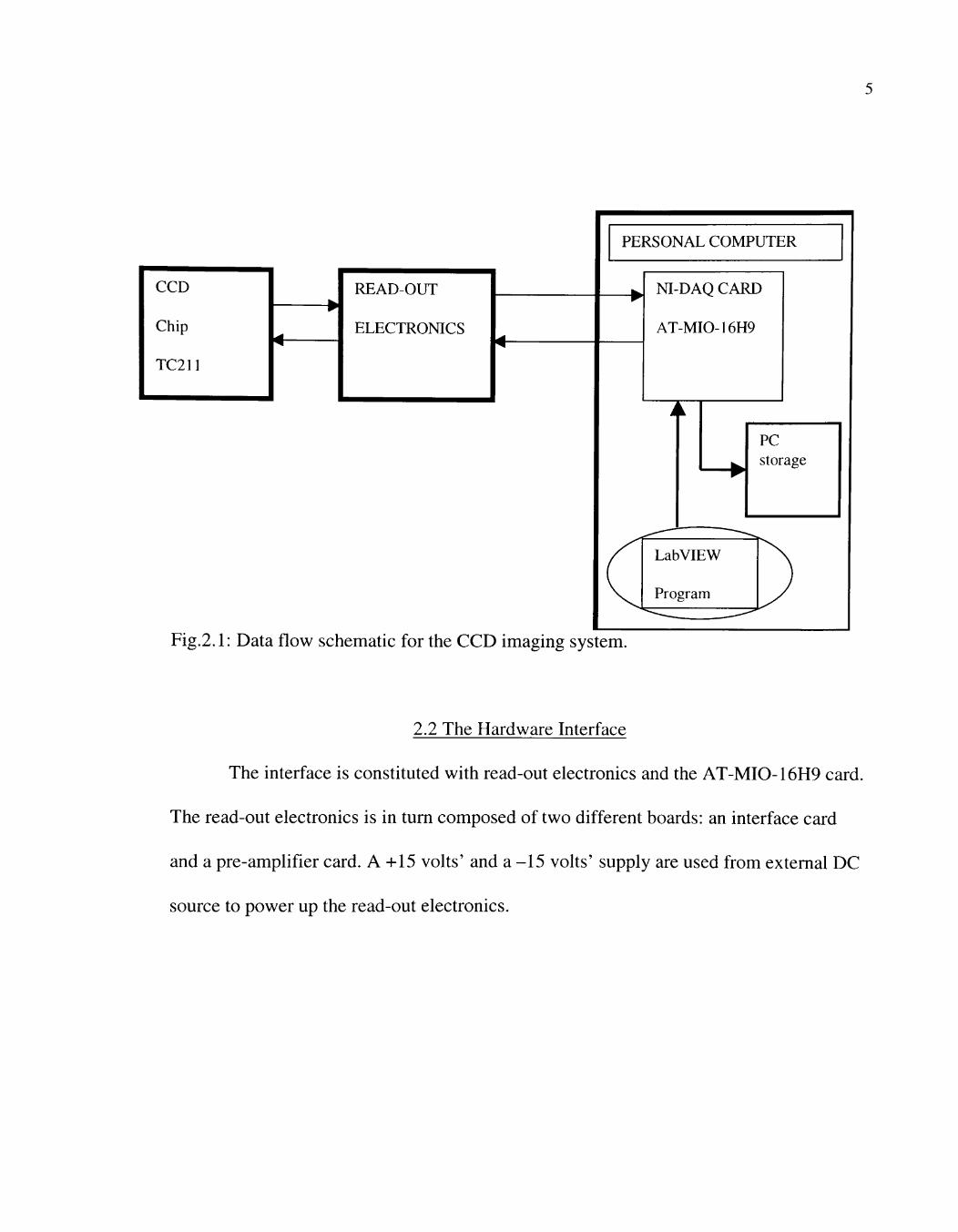
DIGITAL DATA ACQUISITION FROM A CCD CHIP
2.1 Overall System Description
This part of the thesis describes the basic construction and working principle of a
CCD digital imaging system and its control software. The flow of data and/or control
signals between the CCD chip and a PC is facilitated by the use of a hardware interface
(read-out electronics) and a National Instruments' DAQ (Data Acquisition ) card while
the control software has been built using LabVIEW graphical language. The CCD chip
used is a 165 X 192 pixel chip (TC211) manufactured by TI. The NLDAQ card is an AT-
MIO-16H9. After acquiring the data, it is saved in a spreadsheet file. The data flow
diagram is given in Figure 2.1 in the next page.
The first portion of this report describes in brief the functions of the hardware
interface between the DAQ card and the CCD chip. Section 2.3 describes the LabVIEW
user interface and then lists all the user-defined vi's individually. A summary of results
follows in Chapter 4.
CCD
Chip
TC21]
^
^
READ-OUT
ELECTRONICS ^ %
PERSONAL COMPUTER
^ w
NI-DAQ CARD
AT-MIO-16H9
Ii
PC storage
- ^
LabVIEW
Program
Fig.2.1: Data flow schematic for the CCD imaging system.
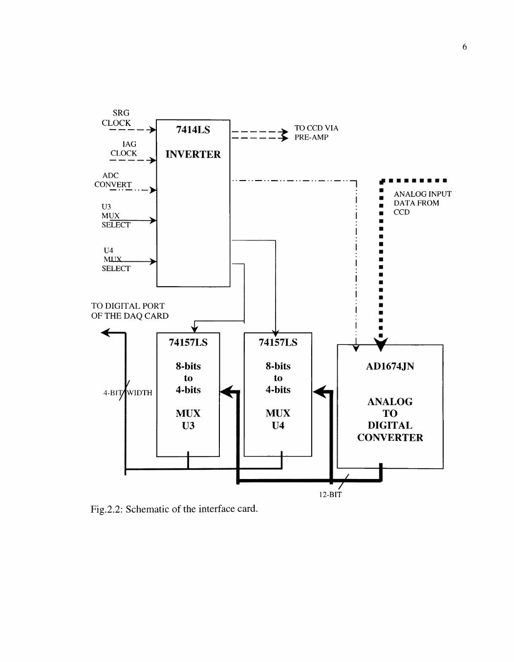
2.2 The Hardware Interface
The interface is constituted with read-out electronics and the AT-MIO-16H9 card.
The read-out electronics is in turn composed of two different boards: an interface card
and a pre-amplifier card. A +15 volts' and a -15 volts' supply are used from external DC
source to power up the read-out electronics.
SRG CLOCK
lAG CLOCK
ADC CONVERT
U3 MUX SELECT
- >
U4 Ml JX. SELECT
7414LS
INVERTER
TO CCD VIA PRE-AMP
TO DIGITAL PORT OF THE DAQ CARD
4-BITy y WIDTH
74157LS
8-bits to
4-bits
MUX U3
74157LS
8-bits to
4-bits
MUX U4
n ANALOG INPUT DATA FROM CCD
AD1674JN
ANALOG TO
DIGITAL CONVERTER
/
12-BIT
t Fig.2.2: Schematic of the interface card.

2.2.1 Interface Card
This card interfaces to the DAQ card on one side and the pre-amp card on the
other. It has five (5) input and four output connections with the DAQ card. Pin
connections are listed in Table A. 1 in Appendix A.
2.2.1.1 Signal Conditioning
The input signals are connected to ground through a RC circuit (not shown in
Fig.2.2) to eliminate high frequency ripple. Then the signals are passed through an LS
inverter. This ensures good TTL signal levels and eliminates noise almost completely.
The inverted SRG and LAG clocks are passed onto the pre-amplifier card. ADC
CONVERT signal is connected to the R/*C pin of AD 1674JN. The MUX SELECT
signals are each connected to the Selection pins of corresponding MUX.
2.2.1.2 Data Conversion And Read-Out
The analog input coming in from the CCD via the pre-amp card is connected to
the input of ADC. When the ADC CONVERT pulse goes from LO to HI the
corresponding inverted signal goes through a HI to LO transition. This HI to LO
transition at R/*C pin of AD1674JN causes the output data lines to be tri-stated and a
conversion is initiated. R/*C must be LO for at least 10 microseconds to ensure correct
values appearing at the output. The 12-bit output is then passed onto the MUX ICs. With
appropriate selection signals the 12 bit data is read in as three 4-bit nibbles (please refer
to Table A.3 in Appendix).

2.2.2 Pre-Amplifier Card
This card has two parts: the clock driver circuits and pre-amplifier circuits.
2.2.2.1 Clock Driver Circuits
CCD chip requires clock signals with voltage levels of-9.5V for LO and + 1.75V
for HI. The clock driver circuits convert the TTL levels to those required by the CCD.
This circuit translates TTL DC level to CCD clock levels with a common-base level
shifter and a MOS clock driver chip, DS0026. The logic LO input to the DS0026 is
referenced with respect to -9.5V instead of ground.
The CCD gates appear as capacitive loads and slow down switching speed of the
DS0026. RC networks and series resistances are used as a counter measure for this. The
series resistance helps to damp ringing and overshoot of the clock signals.
2.2.2.2 Pre-Amplifier
This circuit removes the bias voltage from the raw signal coming from the CCD
chip and amplifies it for the ADC chip. The output from the CCD is buffered with a
unity-gain voltage follower. Then the signal is inverted. The DC bias is subtracted by
using an op-amp. The op-amp output is then fed into the ADC.
2.3 The Control Software
The software is designed to supply the TTL signals and receive the data bits in a
pre-determined hand-shaking fashion. A description of the software below tracks the
operation of the imaging system.
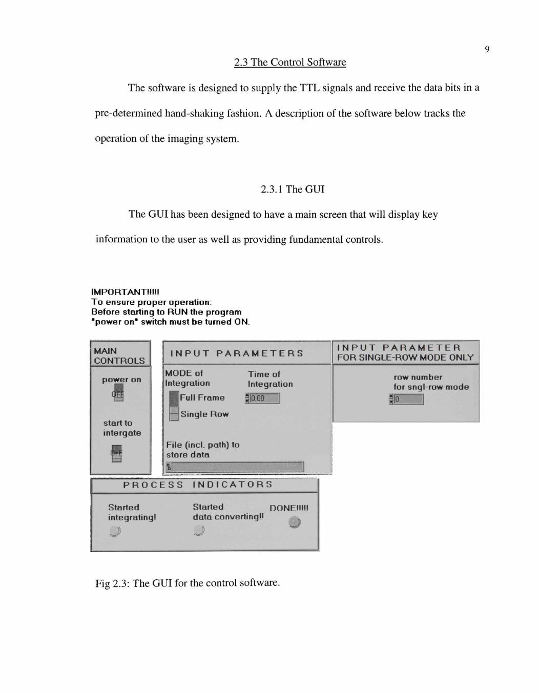
2.3.1 The GUI
The GUI has been designed to have a main screen that will display key
information to the user as well as providing fundamental controls.
IMPORTANT!!!!! To ensure proper operation: Before starting to RUN the program "power o n ' switch must be turned ON.
MAIN CONTROLS
power on
start to intergate
P R O C E S S I N D I C A T O R S
Started Started DONE!!!!! integrating! data converting!! .
I N P U T P A R A M E T E R S
IK Ir
F s
%
10 itE
•il to
DE of T ime of igration Integration
Full Frame jOOO
Single Row
e (incl. path) to ^ H re data ^^m
«^-^«i»~' ^
I N P U T P A R A M E T E R FOR SINGLE-ROW MODE ONLY
row number for sngl-row mode
ilo 1
Fig 2.3: The GUI for the control software.
10
The inputs have their self-explanatory functions. The LEDs turn red when the
indicated function is completed. The main program structure is described below followed
by descriptions of the individual vi's.
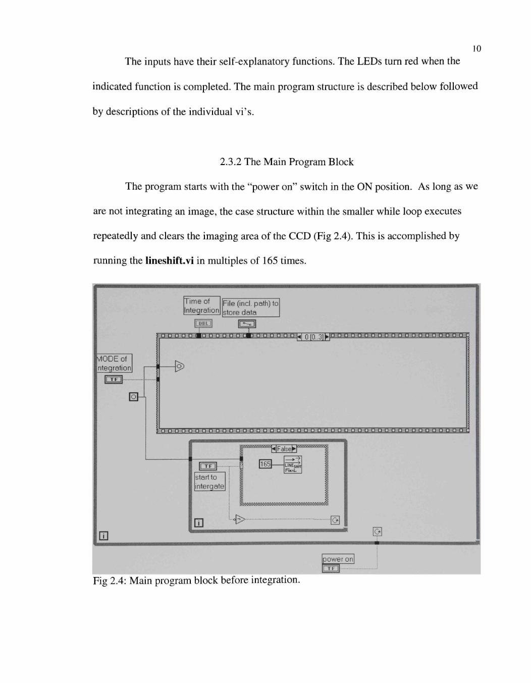
2.3.2 The Main Program Block
The program starts with the "power on" switch in the ON position. As long as we
are not integrating an image, the case structure within the smaller while loop executes
repeatedly and clears the imaging area of the CCD (Fig 2.4). This is accomplished by
running the lineshiftvi in multiples of 165 times.
Fig 2.4: Main program block before integration.

11
2.3.2.1 Integration
After the input parameters (Integration time, Mode of integration, Path name of
the file in which to store data) are entered the "start integration" switch can be turned ON
if an image capture is required. For Single Row mode an additional input parameter
specifying the index of the target row is required.
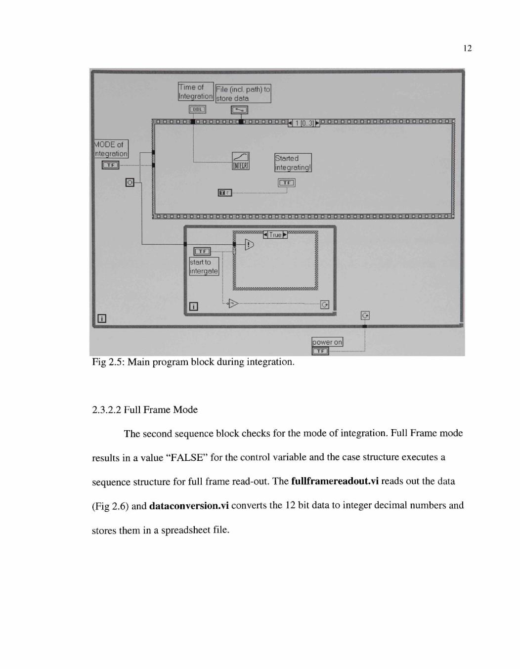
After the "Start integration" is turned on (TRUE) an occurrence is set and it starts
a sequence of program blocks' execution (Fig 2.5). The CCD is supplied SRG pulses and
a constantly LO lAG pulse. The SRG pulses keep clearing out the read-out register at the
bottom of the imaging area while a LO lAG pulse prevents the rows from shifting. This
causes the available optical incidence to be integrated for the specified time. This
function is accomplished by integration.vi.
12
Time of nte gration
File (inci. path) to store data
I
VIODEof nte qrati on
I T F
[2H
• D D D D ma D D g D n cmi D D D D D a ui i m 31 LID D D D D D D n D 0 0 o o n o D n D D D I
^ 1 IH1[[RI
Started integrating!
T F
g D DO n D g DP DP DO DP DPDP nag o an a on a D O pan a n D P a a D P a D a
|ml start to intergate
m •4>- ^
m (-
ovv'eron _ fa Fig 2.5: Main program block during integration.
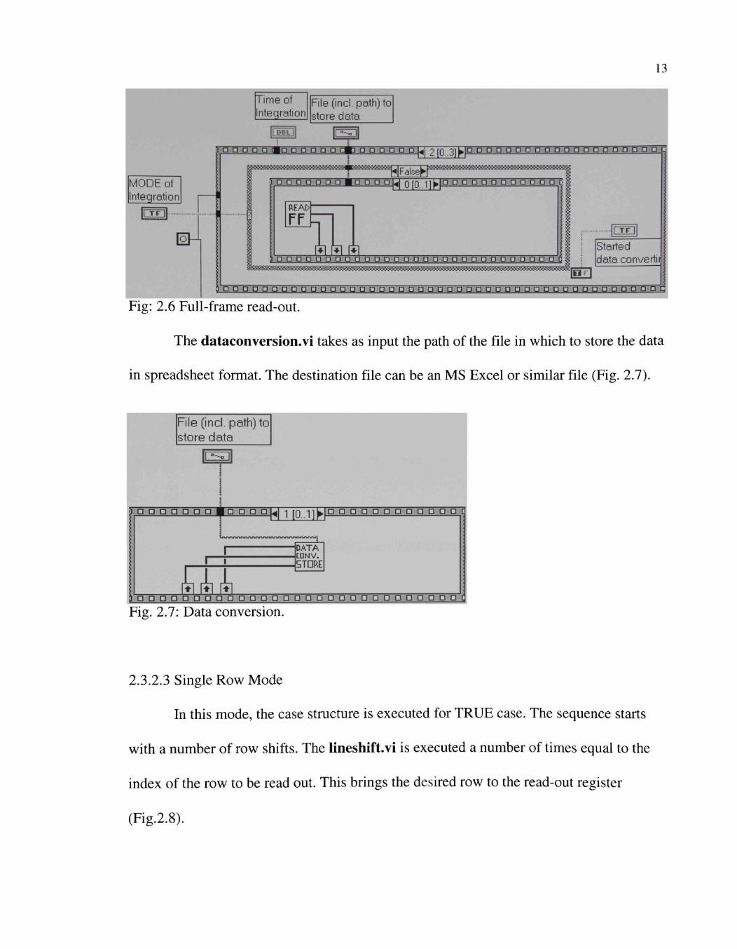
2.3.2.2 Full Frame Mode
The second sequence block checks for the mode of integration. Full Frame mode
results in a value "FALSE" for the control variable and the case structure executes a
sequence structure for full frame read-out. The fullframereadout.vi reads out the data
(Fig 2.6) and dataconversion.vi converts the 12 bit data to integer decimal numbers and
stores them in a spreadsheet file.
MODE of Integration
13
Time of nte gration
File (incl. path) to store data
o p g f w i 0 0 0 0 0 0
^*S«K*:K«^««fl«^KS«'3'ai WM&^A^MfiA^.
2[0.3]h O O O a O O O O O O D O O O O O O O D O
False *-
o o o o o mn a o o Q [Q -) 1 • O O O P a O D D O O O O C g
HM H [ T E J
P O P O O P Q O O O O O P P P P O O P O O O O O O P O C : ^ Started data convertit
0 0 0 0 0 0 0 0 0 0 0 0 0 0 0 OP go p g g o o O D D O D O O O O O O D O O O D D O O O oA Fig: 2.6 Full-frame read-out.
The dataconversion.vi takes as input the path of the file in which to store the data
in spreadsheet format. The destination file can be an MS Excel or similar file (Fig. 2.7).
File (incl. path) to store data
Fig. 2.7: Data conversion.
2.3.2.3 Single Row Mode
In this mode, the case structure is executed for TRUE case. The sequence starts
with a number of row shifts. The lineshiftvi is executed a number of times equal to the
index of the row to be read out. This brings the desired row to the read-out register
(Fig.2.8).
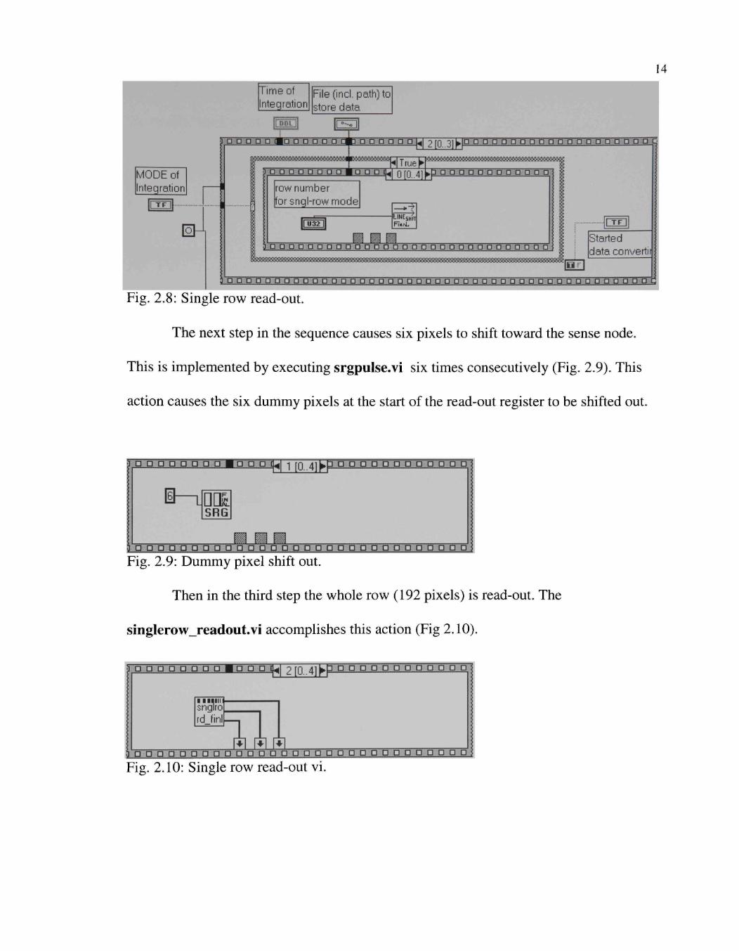
14
Time of nte gration
File (incl. path) to store data
^s] a O O 0 O D M O O O O O O CM3 Q D O O O O UI 2 [0 3]
MODE of Integration
D D D D O g O O D O O O O O D O D D O O
T r u e ^ nnnn aaaoBoo'tai{;| QQ 4 ]^pdadaf td tn j tiatitj
row number for sngl-row mode
i^O 0NEi7n
o o o a p o o p p D O D D D o o o o p p p o o o o a a a a p
OE
MB
started data convertit
p o o a o a a o a O O P 0 0 0 0 0 0 0 0 0 0 0 0 0 0 0 0 0 0 0 0 0 0 0 0 0 0 0 OOP DO o.
Fig. 2.8: Single row read-out.
The next step in the sequence causes six pixels to shift toward the sense node.
This is implemented by executing srgpulse.vi six times consecutively (Fig. 2.9). This
action causes the six dummy pixels at the start of the read-out register to be shifted out.
0 Q g o Q g Q o • Q g p 1^ -| rg 4] ^n a n n a D a a o g a o
HF SRG
5 tjflfl g g B g tjanaaci nnnn o 0.0 go bU p b Q • b Fig. 2.9: Dummy pixel shift out.
Then in the third step the whole row (192 pixels) is read-out. The
singlerow_readout.vi accomplishes this action (Fig 2.10).
g g g g g g g O M g o g i j ^ l 2[0..4]^p g g g a Q D Q o g g a OJ
I i i i i i i i snqiro rd firil
^„w_rhFin '.n n.#i.rtvft.n.n:n.#i'n'rta'i=..Q.a::a a a d d d g ta b d d g b g gS
Fig. 2.10: Single row read-out vi.
15
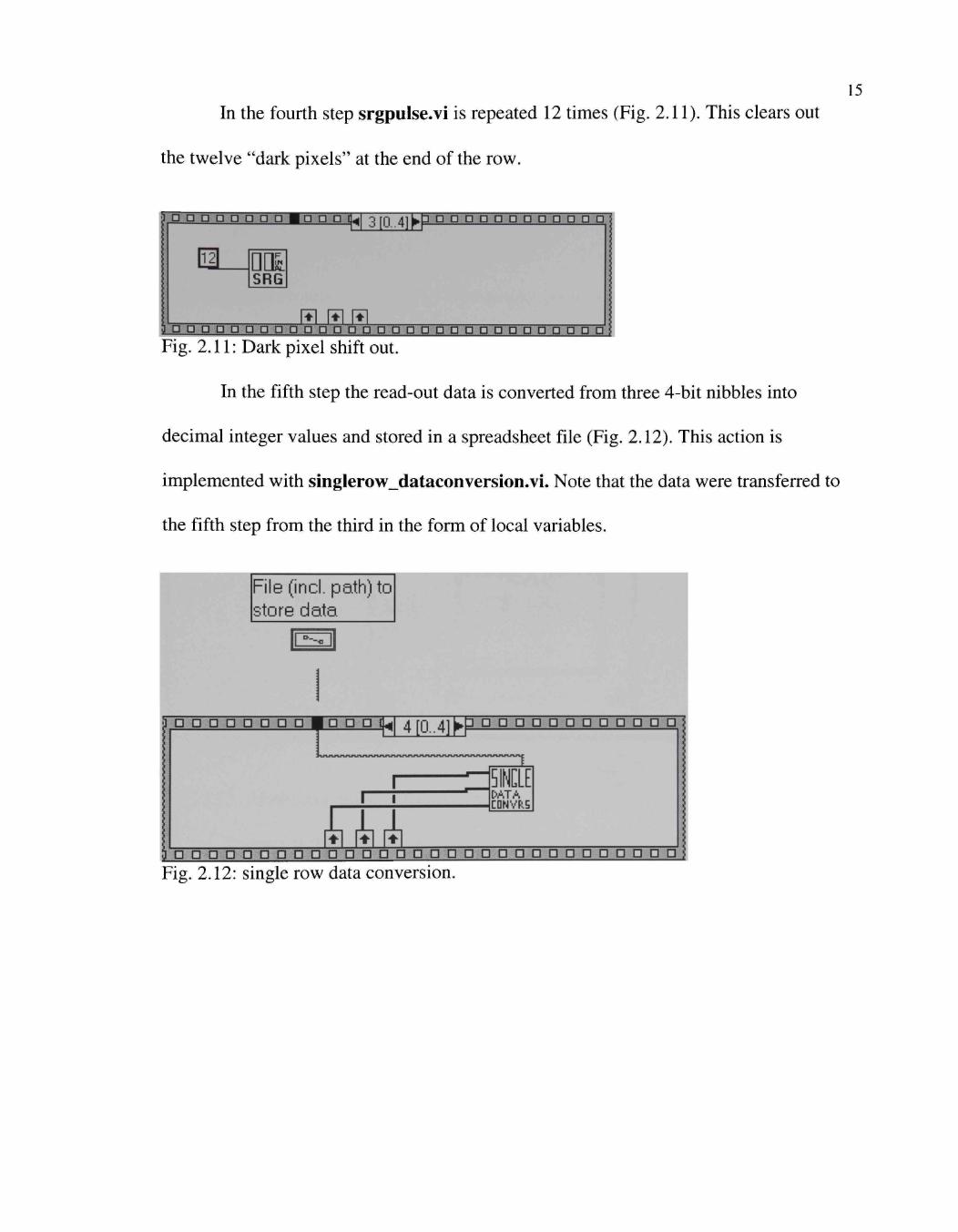
In the fourth step srgpulse.vi is repeated 12 times (Fig. 2.11). This clears out
the twelve "dark pixels" at the end of the row.
f ^ g g H H R j B o o g tui 3m J\]^p p p p j ^ ^ ^ . ^ , ^
• [1 SRG
JSJtLE ,0„b g d,0,::0:::0'd '0'0'"6.d 0 'O'O d b g b b b b d d'0'"0'"b"Ol
Fig. 2.11: Dark pixel shift out.
In the fifth step the read-out data is converted from three 4-bit nibbles into
decimal integer values and stored in a spreadsheet file (Fig. 2.12). This action is
implemented with singlerow_dataconversion.vi. Note that the data were transferred to
the fifth step from the third in the form of local variables.
File (incl. path) to store data
g g o D • D D D • g o g iU| 4 [Q 4] ^ p D o D D D D D g g • g D :
I -5 INCLE I i ' [>ATA
rInrL • • • g g g g g g g g g g g g g g g g g g g g g g g o g g g g g g
Fig. 2.12: single row data conversion.
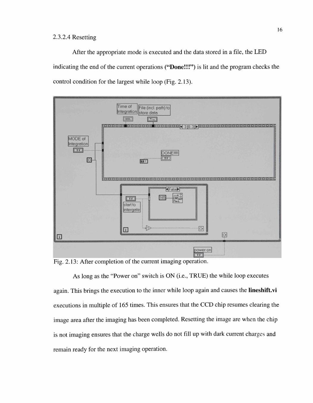
16 2.3.2.4 Resetting
After the appropriate mode is executed and the data stored in a file, the LED
indicating the end of the current operations ("Done!!!") is lit and the program checks the
control condition for the largest while loop (Fig. 2.13).
Fig. 2.13: After completion of the current imaging operation.
As long as the "Power on" switch is ON (i.e., TRUE) the while loop executes
again. This brings the execution to the inner while loop again and causes the lineshift.vi
executions in multiple of 165 times. This ensures that the CCD chip resumes clearing the
image area after the imaging has been completed. Resetting the image are when the chip
is not imaging ensures that the charge wells do not fill up with dark current charges and
remain ready for the next imaging operation.
17
2.4 The Component vi Descriptions
The main program block is composed of several smaller vis which in turn are (in
several of the cases) composed of different vis. Individual descriptions of the vis in as
much hierarchical fashion as possible follows. Only the user defined vis have been
described below, not the library vis.
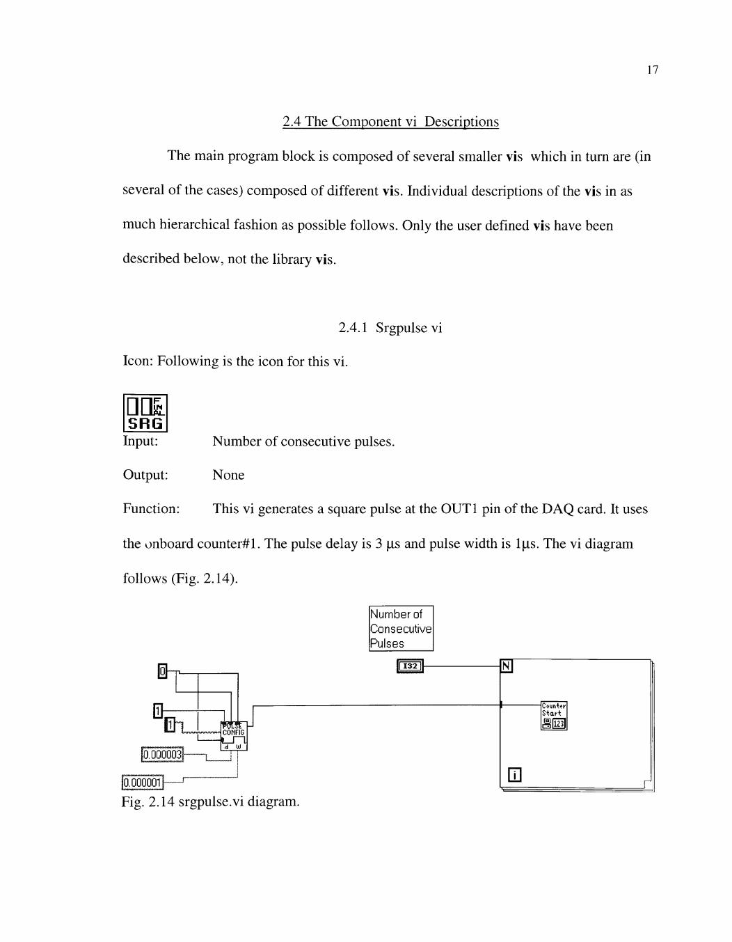
2.4.1 Srgpulse vi
Icon: Following is the icon for this vi.
Input:
Output:
Number of consecutive pulses.
None
Function: This vi generates a square pulse at the OUTl pin of the DAQ card. It uses
the onboard counter#l. The pulse delay is 3 |LIS and pulse width is Ijis. The vi diagram
follows (Fig. 2.14).
&T
a llJl mm
COMFIG
L_r~i
Fig. 2.14 srgpulse.vi diagram.
Number of Consecutive Pulses
[H-
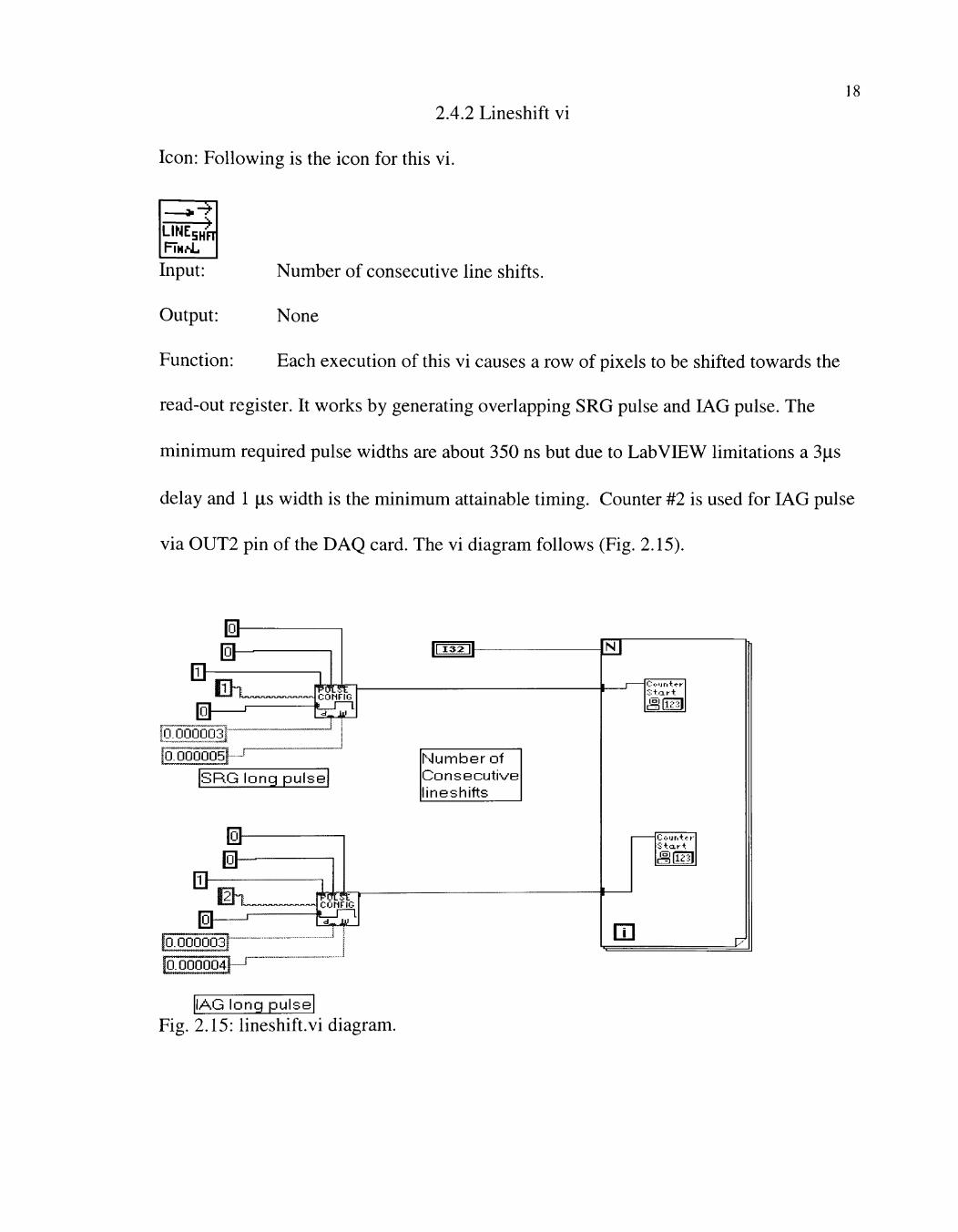
18 2.4.2 Lineshift vi
Icon: Following is the icon for this vi.
r=?
Input: Number of consecutive line shifts.
Output: None
Function: Each execution of this vi causes a row of pixels to be shifted towards the
read-out register. It works by generating overlapping SRG pulse and LAG pulse. The
minimum required pulse widths are about 350 ns but due to LabVIEW limitations a 3|xs
delay and 1 |LIS width is the minimum attainable timing. Counter #2 is used for LAG pulse
via OUT2 pin of the DAQ card. The vi diagram follows (Fig. 2.15).
l2l-
|0.000003|~
0.000005
SRG long pulse
&
&
&
i2h r™^ COMFIG
|o.obooo4H
ir^a^h
Number of Consecutive lineshifts
C-i-'jnt^-r
Icil
S + o r t
m
lAG long pulse Fig. 2.15: lineshift.vi diagram.
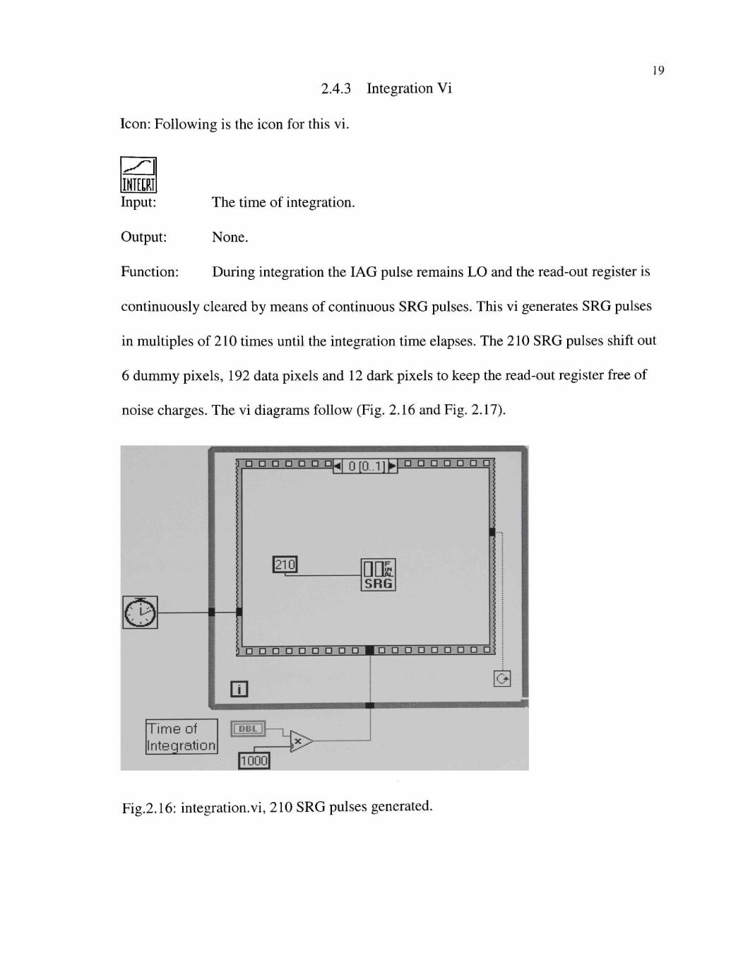
19 2.4.3 Integration Vi
Icon: Following is the icon for this vi.
INI[[RI Input:
Output:
The time of integration.
None.
Function: During integration the lAG pulse remains LO and the read-out register is
continuously cleared by means of continuous SRG pulses. This vi generates SRG pulses
in multiples of 210 times until the integration time elapses. The 210 SRG pulses shift out
6 dummy pixels, 192 data pixels and 12 dark pixels to keep the read-out register free of
noise charges. The vi diagrams follow (Fig. 2.16 and Fig. 2.17).
Fig.2.16: integration.vi, 210 SRG pulses generated.
20
3 a g g g g g QUI -| m - | ] L . [ a D a a a a a J
u-1 K> B>
D O g g g g g g g B g g g g g g o g~g
O
|1 pool
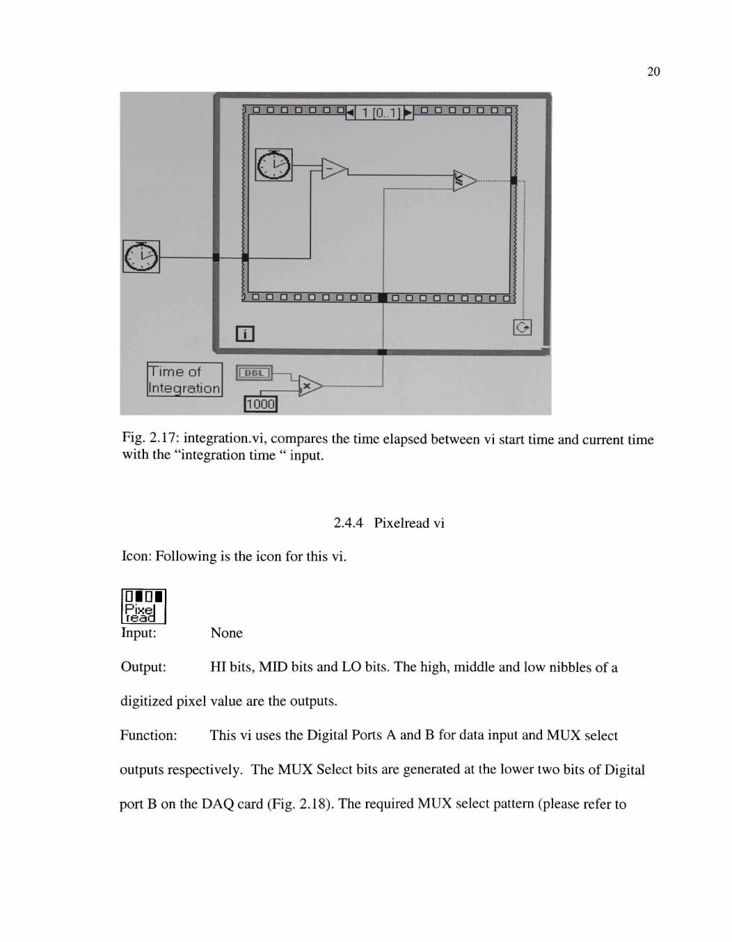
Fig. 2.17: integration.vi, compares the time elapsed between vi start time and current time with the "integration time " input.
2.4.4 Pixelread vi
Icon: Following is the icon for this vi.
Input: None
Output: HI bits, MID bits and LO bits. The high, middle and low nibbles of a
digitized pixel value are the outputs.
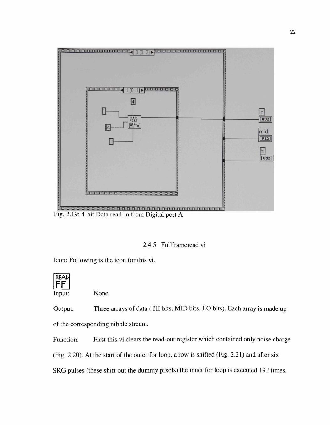
Function: This vi uses the Digital Ports A and B for data input and MUX select
outputs respectively. The MUX Select bits are generated at the lower two bits of Digital
port B on the DAQ card (Fig. 2.18). The required MUX select pattern (please refer to
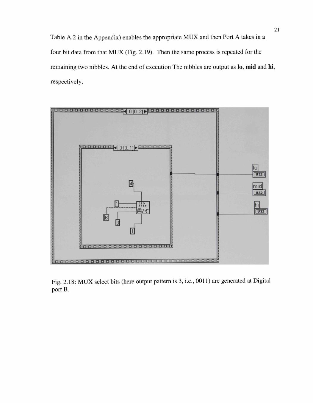
21 Table A.2 in the Appendix) enables the appropriate MUX and then Port A takes in a
four bit data from that MUX (Fig. 2.19). Then the same process is repeated for the
remaining two nibbles. At the end of execution The nibbles are output as lo, mid and hi,
respectively.
o o a a a a o a o D o a a c ^ 0 m..21 •^loaaaQOOoaDaao
g o g o g g Of0..11^ D g g g g g
II
D I G PDRT
& - •
m ET
y'0,.a:...a....d-::.d...d .g..g. d d b g g g b g"PCJi
0'"'0""b' 0 b b b b b b b..b.g-.-b b.o a,:.o,,b.....g......g....g..g b .b b b.b,..g.g..g..o
Fig. 2.18: MUX select bits (here output pattern is 3, i.e., 0011) are generated at Digital port B.
22
p a D D a o D g g g D g g n ^ i Q m 2]kp ° ° ° Q Q a a a a a a D D C
i g g g o g g ^ -j [Q -jj ^ D a g g g o a -
i &
P O R T
Q -
a g g o o o o g D a o o D a a a o o
g o g o g o g o o g g o o o o g o o a o ODD go O P O O g g g Fig. 2.19: 4-bit Data read-in from Digital port A
2.4.5 Fullframeread vi
Icon: Following is the icon for this vi.
Input:
Output:
None
Three arrays of data ( HI bits, MID bits, LO bits). Each array is made up
of the corresponding nibble stream.
Function: First this vi clears the read-out register which contained only noise charge
(Fig. 2.20). At the start of the outer for loop, a row is shifted (Fig. 2.21) and after six
SRG pulses (these shift out the dummy pixels) the inner for loop is executed 192 times.
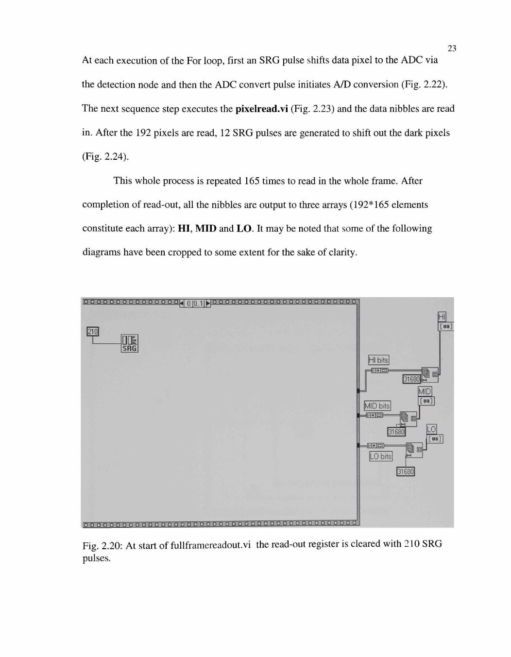
23 At each execution of the For loop, first an SRG pulse shifts data pixel to the ADC via
the detection node and then the ADC convert pulse initiates A/D conversion (Fig. 2.22).
The next sequence step executes the pixelread.vi (Fig. 2.23) and the data nibbles are read
in. After the 192 pixels are read, 12 SRG pulses are generated to shift out the dark pixels
(Fig. 2.24).
This whole process is repeated 165 times to read in the whole frame. After
completion of read-out, all the nibbles are output to three arrays (192*165 elements
constitute each array): HI, MID and LO. It may be noted that some of the following
diagrams have been cropped to some extent for the sake of clarity.
:fm.;,. m..:>rm:'.:^rff;:.mm:y:^n .:ihrf.?.:lwT>',:-^nt:li rwit-Jwr.'.!*w*>.:-*w*.<^rtr.:•:-.hn. ^ U I U I I .w '• .•wri',r^rw ..^m..^rf...im...frm...frir...M^...frm...frff....^nr....yi^...ym...ftrr....irif...Xm.^ ,.rm.-
SRG
a d a ci 5 a 0 0 g g a D 0 a 0 a o a 0 B a a'ft g a B d &oa-ofro-a a-o-tro BTFi
Fig. 2.20: At start of fullframereadout.vi the read-out register is cleared with 210 SRG pulses.
24
fa fa g a d a d a o b o d d d Q D 0 0 t tj b gj^i T |u -|j |UILJIU.o 0 tj Q b g d t i 0 0 d 0 fa ft D a ti D D-gi
in
J ^ 10.0000031
nrarer COMFIG
p.oooGisr
w a a o a o a a o o D a a c | ^ | Q [Q 3]^p a o o o o o a o o a D d g
FTMAL
m fa' '.'d' ' .faliMJidia'. 'd ' b '0"d' 'H' '0"'0"'a"'d"'d' fa"d' 'd"'a' "[|3"'|;j-[;3"'a'".'i3' a"'tj' 'd ' fa'
Fig. 2.21: A row is shifted.
g D g Q D g g D o D D g o Q g o g g g g D g g 1 [01] g g g g g g g g o g g g g g o g g g ^
m
l2h
rwrar COHFIG
I 1
g g g g g o p g g g o o tui 2 m 3]kP g g g D O g o g 0-0
ET
m
i g a D D g n^i Q [Q 11 kP g g g g g"^
SRG
Count<-K Start
m g g o g a o g a o g g a o a a g
o-d'"d fa a fa Q fa'-'O: fa-fa.B d fa .a .fa fa fa: a a a .fa-fa-'a"a 'a a 'a'.:i
g o o g g o g p n o o g o o g o g g g g g o g D g g o g o o g g g a o g g 0.0 o,g„g,o„g..o...g..i
Fig. 2.22: After one SRG pulse an ADC Convert pulse is produced ("counter start vi" in the innermost loop).
25
Q • o o g g o Q g o p o g g g g o a o o a a a[^| -| [Q - | ] ^ | a a D a D O D D D D O D D a a a an UZ
m
0,000015
^
F
m
I*—* iiiTrPiniTTf iiMVfirimTfrrirfrTfiiiifTTTfrMihTftMjrTTl..ii%Tf.iiiflTfii.ii^^ ^ Z l M J -.IJ I ^ ^ ^...yrr' ...*Trt ...frrrt ..*Tr^ .l.trnt.. *>«* ..*rrA...\m* ^.*r-A \rJ . l»-j. -. * i
ET g Q g g g c i m -| i ^ 3 g g g g g
OIDI Pixel read
m O'0'a"fa"'0"'fa""0"0'0 0 fa '0"d"d'fa''0'
i g g g g g g g g g g g g g g g g g g g g g g a p a p g o a p g o nna g g g g g g g g g c
Fig. 2.23: Each pixel is read in from the MUX outputs with pixelread.vi.
3 g a g D|^| -| [Q i ] ^ [ a O O O g o p p g o o o g g g g g g g g g p o
3 D g g D Q o n a g g D t } ^ | 3 [Q 3]^p.iP g g ummamris^-u g g g g t:
[ •O^ SRG
' a a d a b d O O O f a f a d d d O O d d d tJ-OO H d d d Q-Q-g-Q-
5"o::a:::-a oQ.Q-a-d d Q d..o.:a.j.Jafa':d:d>da oa.d Q o d.a a d d d d' Fig. 2.24: 12 SRG pulses clear out the dark pixels after a row is read-in.

26 2.4.6 Dataconversion vi
Icon: Following is the icon for this vi.
Input: Three arrays - HI, MID, LO and a file path name. Each array is composed
of 31680 4-bit nibbles.
Output: None
Function: This vi takes in the three arrays of nibbles and converts them to decimal
integers. The inner for loop takes care of one pixel data at each execution. The nibbles are
logically shifted and concatenated to result into a 12-bit integer (Fig. 2.25). After
converting the whole frame data, the results are stored in decimal form in a file whose
path and name is specified as an input. The input file name should have *.dat extension
to facilitate ASCII export to a spreadsheet program.
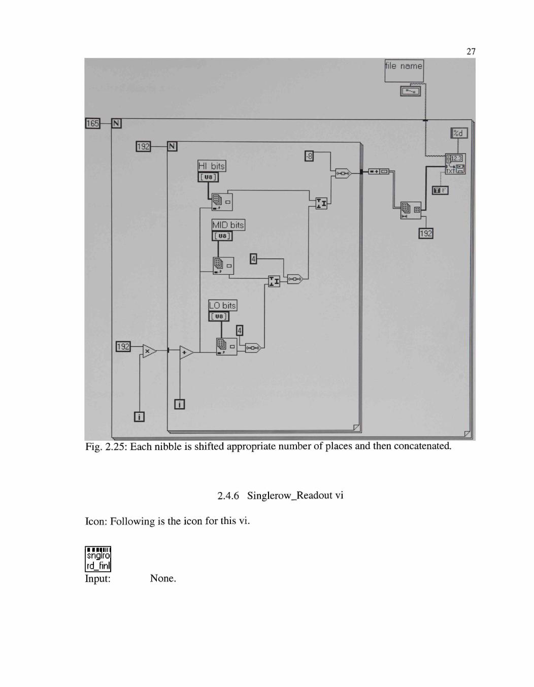
Fig. 2.25: Each nibble is shifted appropriate number of places and then concatenated.
2.4.6 Singlerow_Readout vi
Icon: Following is the icon for this vi.
• I I I I I I I sngiro rd_finl Input: None.
28 Output: Three arrays, each composed of the Hi, Mid and Lo nibbles of the
digitized data in a row of pixels.
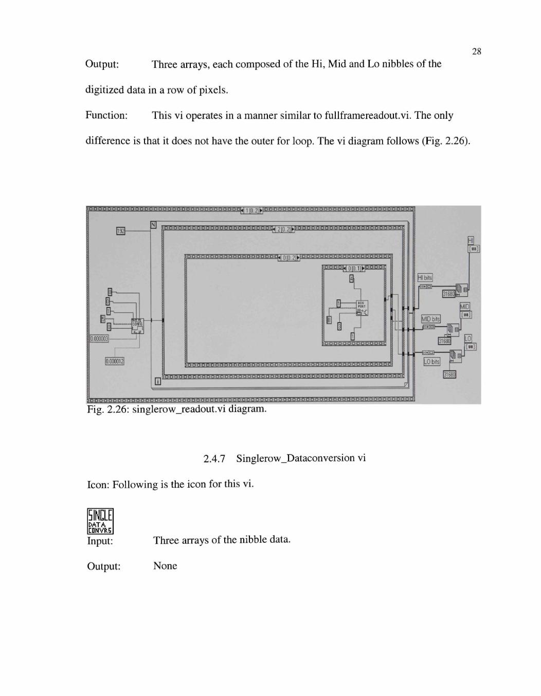
Function: This vi operates in a manner similar to fullframereadout.vi. The only
difference is that it does not have the outer for loop. The vi diagram follows (Fig. 2.26).
pjocijggociajoeiaaojDQiaocaiOtDaao^^^ 1 [0 2]^°:"-^'°^°°'^^^-°°'°^^^^^^
192 iHr
ih-
ir: COWIG
M O O O ^ - ^
0.000012
Q
HattflBHBft.BociflflBt)saij''flDgBaq^|2[o.2iKpflBaBflBasaaBaBaiJBOflBHaflB-
mBwcmmj!^aixxmMmiCftixmts:<ixq^ \]\j] 2]ypas^smMnmaami.MMM^!:fi:ias^
|4|
.Jb OK' fOKT
f gpoggODDgDn^oa
BBaBBBflHBHflflBHaaBBBflBBttSBBHBHBBDflBBaaflBtlOa-B-g-dJ
BBaflBBBflttBaflflBflaflBBBflBBBaflBHaaBBBaBfloaBBBBaBaaoBaaaa
feaaaBBaflHaaaflBaaaBaBaBBaaflBBaaBBaaBBBaaBBaaBaaaBBBaaBBaaBBaoooaaaBoaffng.
Fig. 2.26: singlerow_readout.vi diagram.
2.4.7 Singlerow_Dataconversion vi
Icon: Following is the icon for this vi.
5INCLE DATA CDMVRS
Input:
Output:
Three arrays of the nibble data.
None
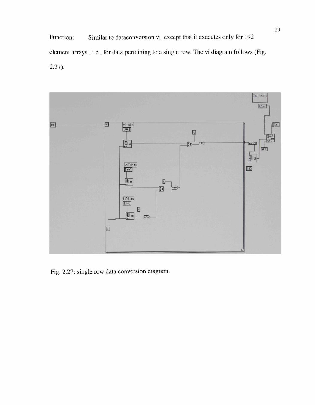
29 Function: Similar to dataconversion.vi except that it executes only for 192
element arrays , i.e., for data pertaining to a single row. The vi diagram follows (Fig.
2.27).
Fig. 2.27: single row data conversion diagram.
CHAPTER 3
CONTROL OF A MAGNETRON SPUTTERING EQUIPMENT
3.1 Svstem Description And Control Flow
The Magnetron Sputtering equipment is an Endura® HP PVD system
manufactured by Applied Materials, Inc. This equipment has several peripherals that are
to be controlled using LabVIEW and eventually brought under an integrated control
interface. A microcomputer has been used as the front-end interface.
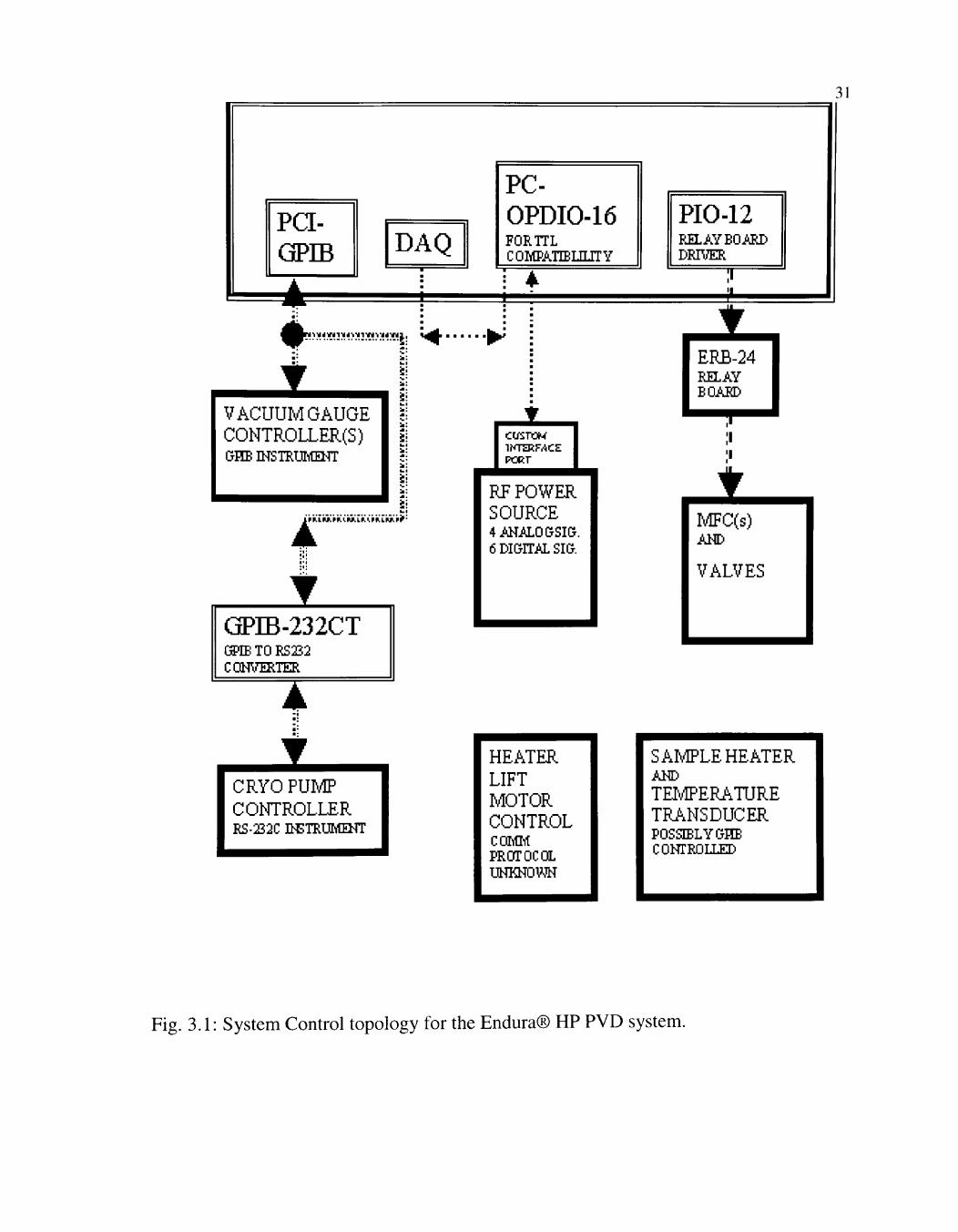
As portrayed in the Fig. 3.1, the total system has been broken down into several
constituent sub-systems. Each sub-system is to have its own control software that will
engage its communication with the PC.
30
31
PC-OPDIO-16 FOR TTL COMPATmUUTY
VACUUM GAUGE CONTROLLER(S) CJHE INSTRUIrtlMT
LPK.
i
pkLUpiiiiMiifiilpiCiuF^
GPIB-232CT GPIB TO ES232 CQNVHtlER
X
CRYO PUMP CONTROLLER KS-232C nCTRUMHTT
PCRT
RE POWER SOURCE 4 A H A L 0 I J S I I J .
6 DIGITAL SIG-.
PIO-12 ERAYEOAED DEIVER
T
MFC(s) AND
VALVES
HEATER LIFT MOTOR CONTROL COMIrt PEOTOCOL UbffiHOWN
SAMPLE HEATER AND
Te^ERATURE TRANSDUCER POSSIBLY GHE CONTEOLLED
Fig. 3.1: System Control topology for the Endura® HP PVD system.
32 3.2 The Sub-Systems & Hardware Set-Up
At least six sub-systems have been defined and identified. They are :
a. The Vacuum Gauge Controller(s) i.e. VGC.
b. The Cryo-pump controller.
c. The MDX RF Power Source.
d. Valve system, including MFC valves and load gate valves.
e. Sample Heater temperature/power control.
f. Heater lift motor control.
The interfacing hardware within the PC includes the PCI-GPIB controller card, a
DAQ card (PC-MIO-16E4), a digital I/O card (PC-OPDIO-16) and a relay board driver
card (PIO-12). The VGC has a built-in GPEB interface that leads to its being controlled
by the GPIB controller. The Cryo-Pump controller is an integral part of the On-Board 8F
cryogenic pump manufactured by the CTI-Cryogenics. The cryo-controller has an RS232
serial interface for remote operation. By using the GPIB-232CT converter, the cryo-
controller can be added to the GPIB bus.
The Power source has a 15-pin custom interface connector for remote operation.
The control signals include four analog and six digital signals. The DAQ board is capable
of furnishing these signals except for a few digital signals whose HI level is 15 volts. To
tame these signals to a TTL compatible level a Digital I/O board is to be used in between
the power supply interface and the DAQ card. The PC-OPDIO-16 can detect and
generate signal levels of up to 24V. Thus it can translate a 15V DC detected signal into a
5V DC generated signal and viceversa.
33 An external relay board ERB-24 is to be driven by the relay driver PIO-12. The
external relays will operate MFCs and also actuate the loading / unloading valves.
The sample heater temperature can be controlled using a temperature transducer
feedback. This sub-system may be added to the GPIB bus with appropriate hardware
interfacing that may or may not be needed. The heater lift motor control is the remaining
sub-system whose hardware interface, hence the communication protocol, is yet to be
decided upon.
Most of the hardware described above has been installed and the infrastructure
has been set up. The two parts of the system which have been successfully completed -
the main software control structure and the VGC control, will be described in the
following sections.
3.3 The Software
3.3.1 Main Control Panel
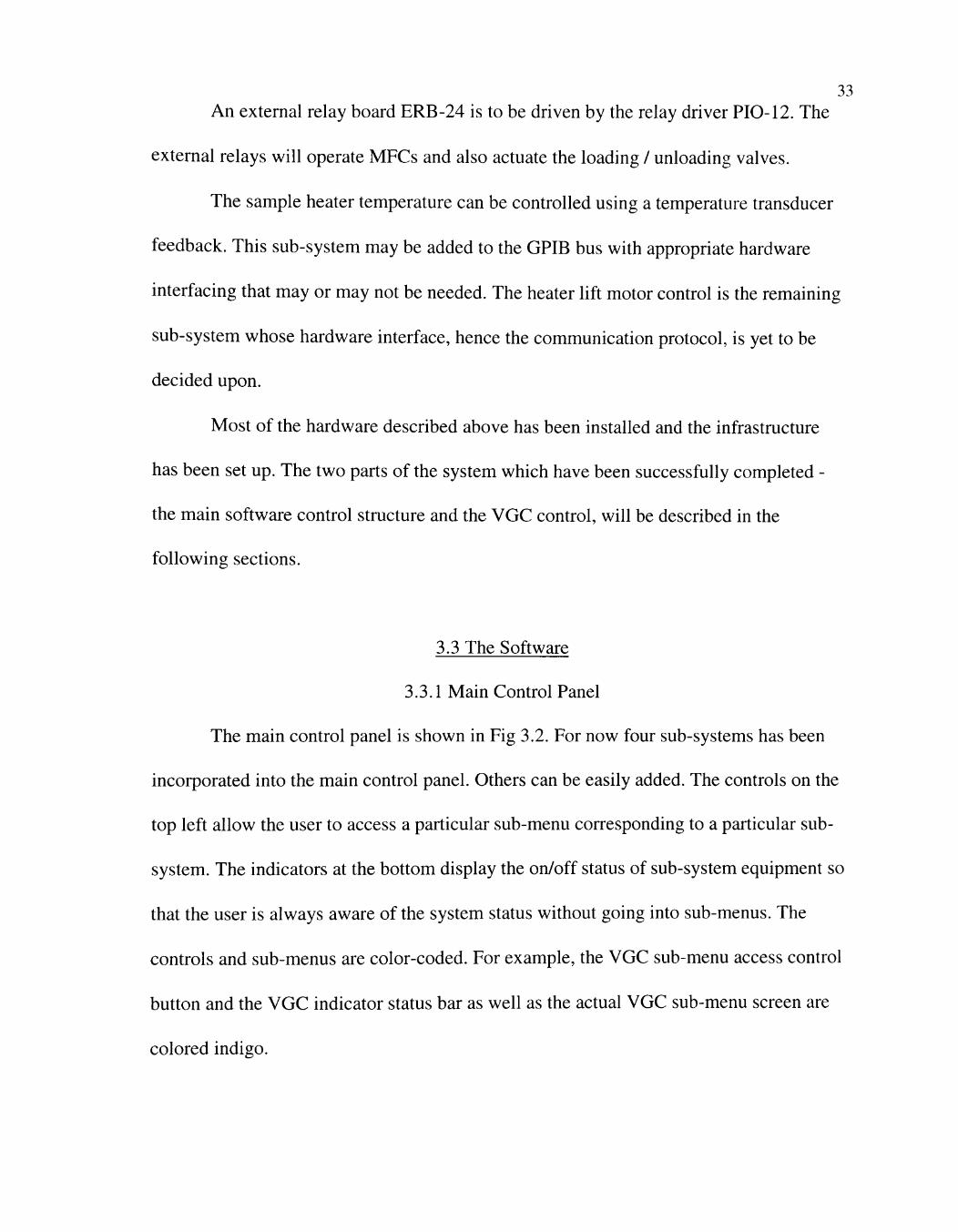
The main control panel is shown in Fig 3.2. For now four sub-systems has been
incorporated into the main control panel. Others can be easily added. The controls on the
top left allow the user to access a particular sub-menu corresponding to a particular sub
system. The indicators at the bottom display the on/off status of sub-system equipment so
that the user is always aware of the system status without going into sub-menus. The
controls and sub-menus are color-coded. For example, the VGC sub-menu access control
button and the VGC indicator status bar as well as the actual VGC sub-menu screen are
colored indigo.
34
VGC ContiD IP a n e l
CRYO Con t t c i lPane l
Opera to r
A A
J H B H H H M I I H I H M H H B H I E l E 2 DEGAS
H jl jl ;
1
1
Figure 3.2: The Main Control Panel.
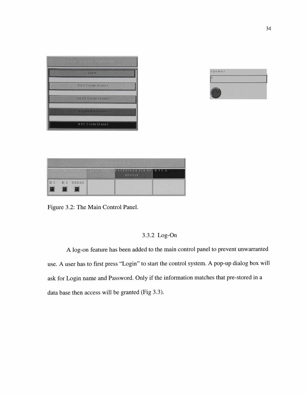
3.3.2 Log-On
A log-on feature has been added to the main control panel to prevent unwarranted
use. A user has to first press "Login" to start the control system. A pop-up dialog box will
ask for Login name and Password. Only if the information matches that pre-stored in a
data base then access will be granted (Fig 3.3).
35
Log ri N am e
P a s s w ord
m
*
0 K 1 C a n c e l
O K
(a) (b) (c)
Figure 3.3: Accessing (a) Login prompt, (b) Login match found, (c) not found.
After access has been permitted, the user name will be displayed on the right hand
top corner of the main control panel. At this time all the indicators will show the true
status of the system and the user can access one or more sub-menu as need arises. The red
button "Quit" can be pressed at anytime to quit the program. The system status will
remain whatever it was just prior to quitting. Any desired status change has to be
accomplished by explicit action by the user, nothing will turn off if the program is
quitted.
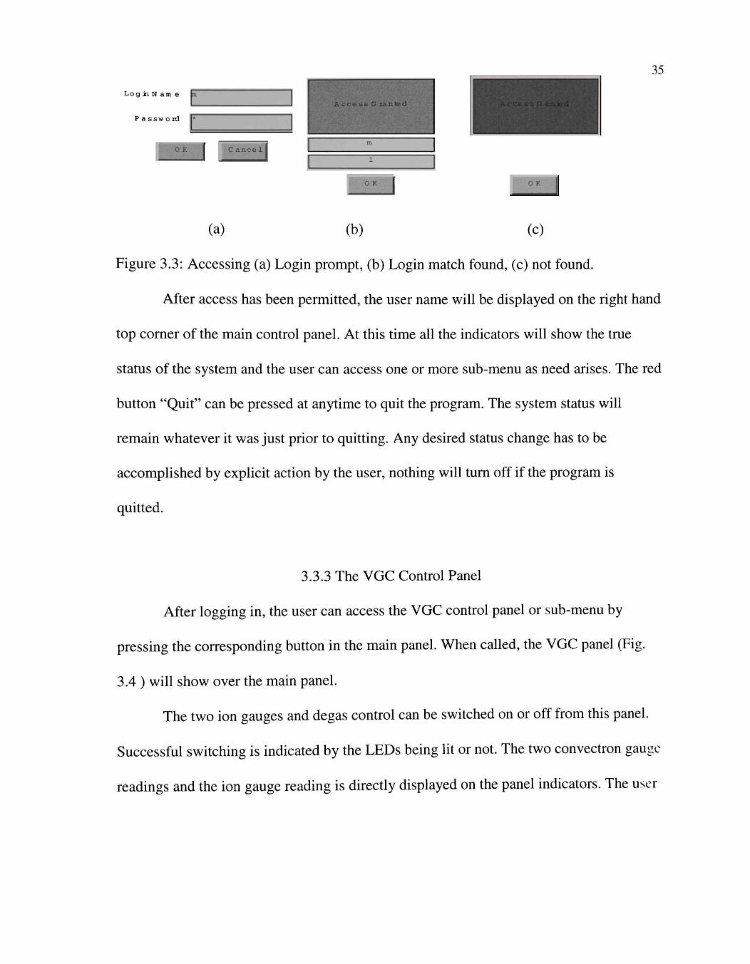
3.3.3 The VGC Control Panel
After logging in, the user can access the VGC control panel or sub-menu by
pressing the corresponding button in the main panel. When called, the VGC panel (Fig.
3.4 ) will show over the main panel.
The two ion gauges and degas control can be switched on or off from this panel.
Successful switching is indicated by the LEDs being lit or not. The two convectron gauge
readings and the ion gauge reading is directly displayed on the panel indicators. The user
36 can close the panel without disturbing current state of operation and go back to the
main panel where the indicators will continue to show the current VGC system status.
DEGAS
ON
loFF
DEGAS STATUS
E 1
ON
OFF
El STATUS
E 2
ON
OFF
E2 STATUS
PRESSURE READUGS
D N G U AG E
TORR
C O N V E C T R O N A
C O N V E C T R O N B
TORR
TORR
NOTE : 9 50E+09Readi ig i id ia tBS thatcorr-espondi ig guage E O F F .
C LO S E T H S P AK E L
Figure 3.4: The VGC control sub-menu.
3.3.4 Other Controls
The other sub-system control panels can be accessed in a manner similar to that
for the VGC control panel. Appropriate indicators for each sub-system can be easily
incorporated into the main control panel.
37 3.4 The Component Vis
3.4.1 Main Control Vi
Icon: Following is the icon for this vi.
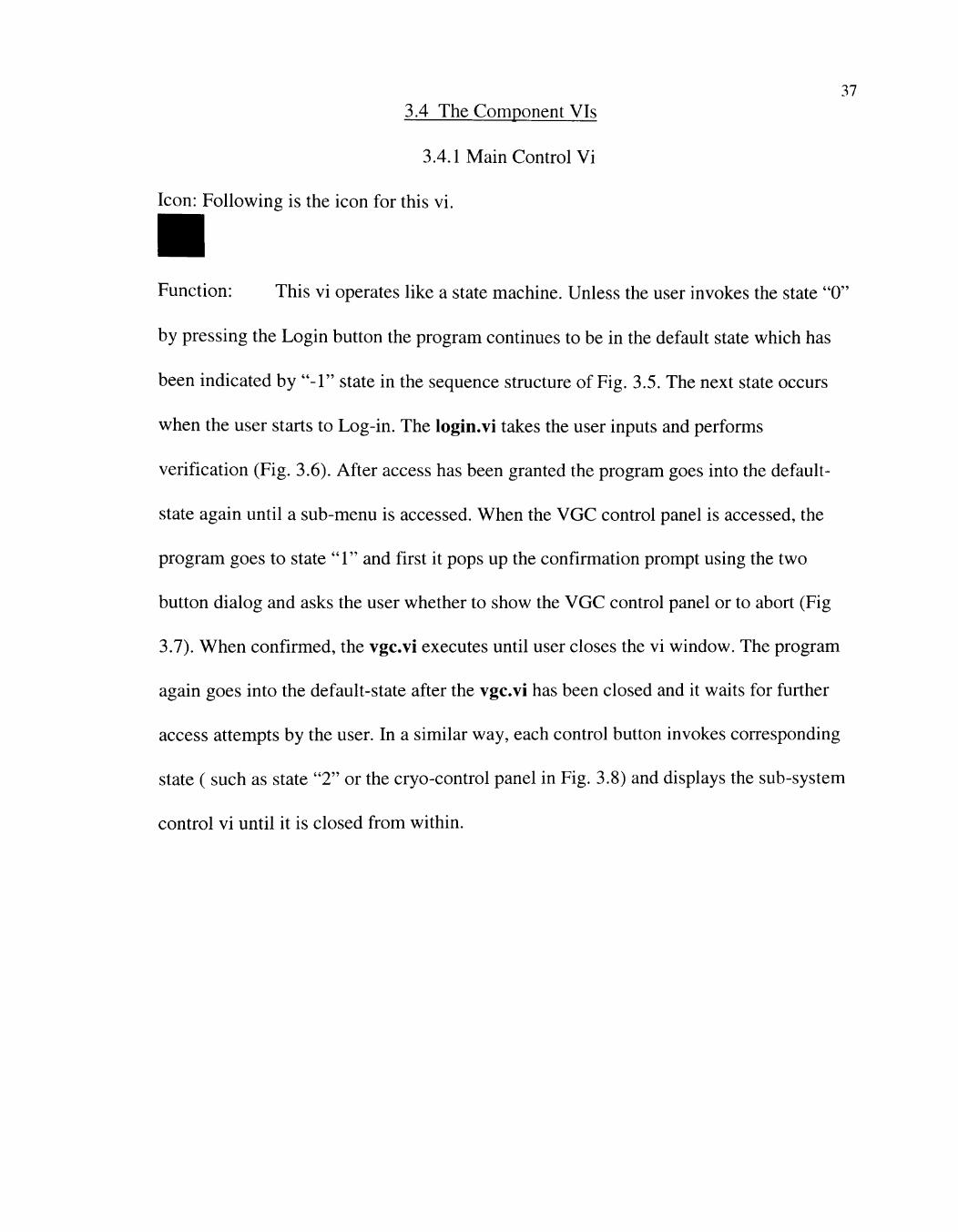
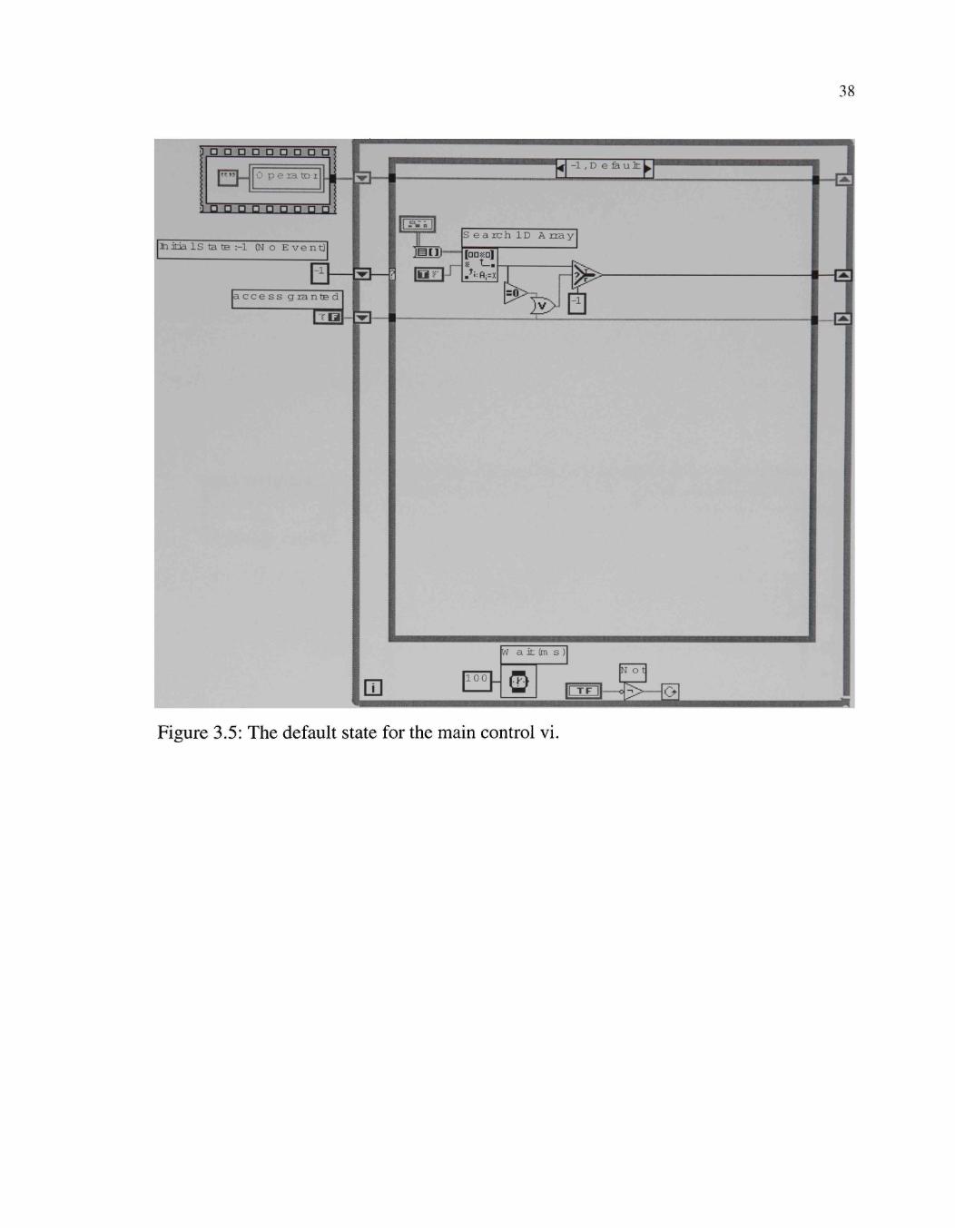
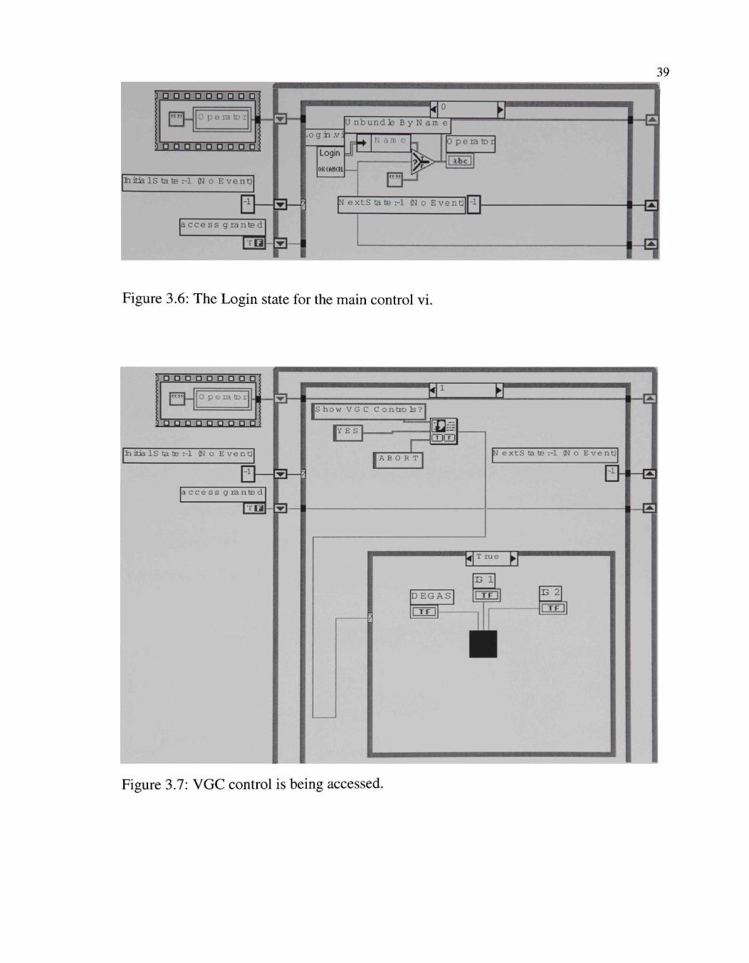
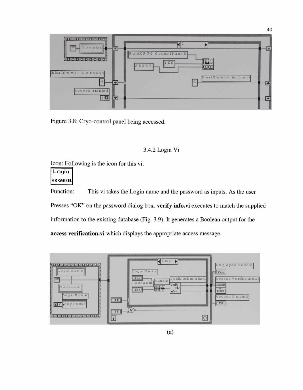
Function: This vi operates like a state machine. Unless the user invokes the state "0"
by pressing the Login button the program continues to be in the default state which has
been indicated by " - 1 " state in the sequence structure of Fig. 3.5. The next state occurs
when the user starts to Log-in. The login.vi takes the user inputs and performs
verification (Fig. 3.6). After access has been granted the program goes into the default-
state again until a sub-menu is accessed. When the VGC control panel is accessed, the
program goes to state " 1 " and first it pops up the confirmation prompt using the two
button dialog and asks the user whether to show the VGC control panel or to abort (Fig
3.7). When confirmed, the vgc.vi executes until user closes the vi window. The program
again goes into the default-state after the vgc.vi has been closed and it waits for further
access attempts by the user. In a similar way, each control button invokes corresponding
state ( such as state "2" or the cryo-control panel in Fig. 3.8) and displays the sub-system
control vi until it is closed from within.
38
Figure 3.5: The default state for the main control vi.
D a D D D D D a D
0 vj e IB to i iC ••8CriiiiB_HaABaHSK«aSs(iaiiABiMaBBiiadBHiS
IiitH IS ta tE :-l (N o E v e n t )
U n b u n d l e B y N a m e
o g m .V:
Login JP N a in e
a c c e s s g r a n t E d
N a m e
0 p e ra to r
i i b c
N e x t S ta tE :-l (No E v e n t )
a'.ir!W'K'''\T-''/*?/:-'>''' ^-"
Figure 3.6: The Login state for the main control vi.
g o n D P D D g D ;
O p e la t]:> r . | _ Pjr
0::'O":a""0""a o o tj'i:;:
l i i t ia I S ta tE :-l (N o E ven t : )
Is h o w V G C C o n t r o t e ?
lY E S CDCD
A B O R T N e x t S ta tE :-l CN o E v e n t )
T rue
D E G A S
E 1
T F
T F
B
E 2
T F
Figure 3.7: VGC control is being accessed.
40
Figure 3.8: Cryo-control panel being accessed.
3.4.2 Login Vi
Icon: Following is the icon for this vi.
Login OKCAMtEL
Function: This vi takes the Login name and the password as inputs. As the user
Presses "OK" on the password dialog box, verify info.vi executes to match the supplied
information to the existing database (Fig. 3.9). It generates a Boolean output for the
access verification.vi which displays the appropriate access message.
I g D g g D o g g g p g c'
) c jn K a III e
P a s aw o rS
D ;
Lo g m N am e
( K e y F o c u s
g g g g g g g g g g g d
L (a)
41
D o a D D a a D D a a i c; jri K a rii e
P a s s w Old
L o g n N am e
m >Key F o c u s
•ABiMft&aMBBMA^BXaMdBaHfl^^^flB^^B^^^flB^BdB^^H^L
(b)
Fig. 3.9: The login vi (a) verifying information, (b) the "Cancel" case.
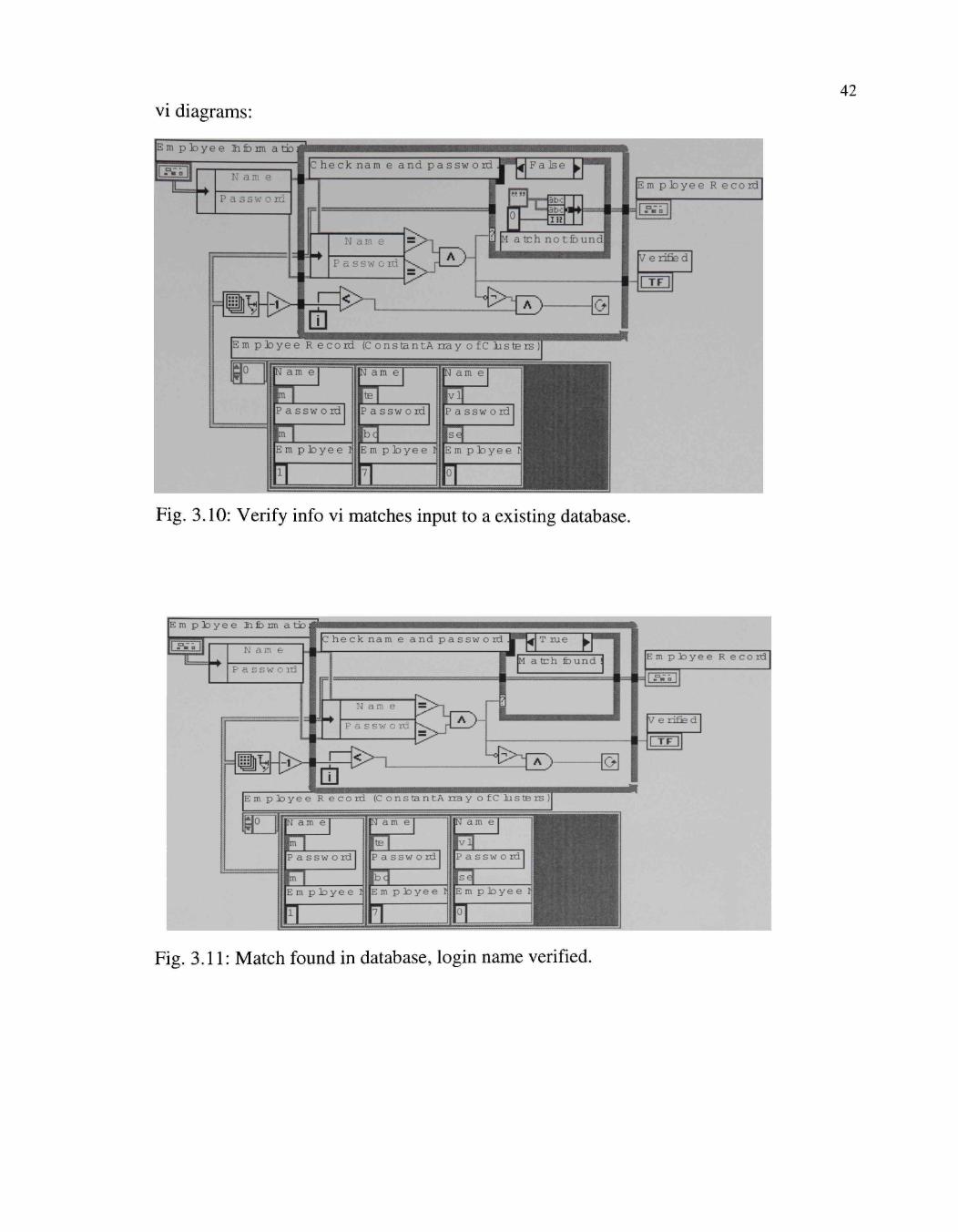
3.4.3 Verify Info vi
Icon: Following is the icon for this vi.
Function: This vi takes the user (or employee) login name and password as inputs. It
has a pre-existing constant cluster array which acts as the database. If a match is not
found (Fig. 3.10) a FALSE Boolean output is generated. In case of match (Fig. 3.11), a
TRUE output is generated for the access verification.vi.
vi diagrams:
Em p t o y e e Iiform a t b
P a s s v; o rd
B>
c h e c k n a m e a n d p a s s w o r d
rl a -R
Pass ' , ' ! c lu
U^ d]
E m p l o y e e R e c o r d (C o n s t a n t A n a y o fC l i s t s rs
am e
P a s s w o rd
E m p l o y e e l|
T
P a s s w o rd
be
m p l o y e e I
[N am e
F^ |P a s s w 0 rd
| s e
Em p toye e I
0
Fig. 3.10: Verify info vi matches input to a existing database.
42
Em p D o y e e liform a t i )
N a;n e
P a K a w o vd
C h e c k n a m e a n d p a s s w o
N a m e
. s s v; G ixi
T rue
a tch fc u n d
BSH5> ^ : E ) Em p ]o y e e R e c o r d (C o n s t a n t A n a y o f C i a s t e rs )|
P a s s w o rd
E m p to y e e I
K
[ N a m e
O IF a s s w o rd
F E m p to y e e r
^
Em p t o y e e R e c o r d
S^h
V e rdfie d
Fig. 3.11: Match found in database, login name verified.
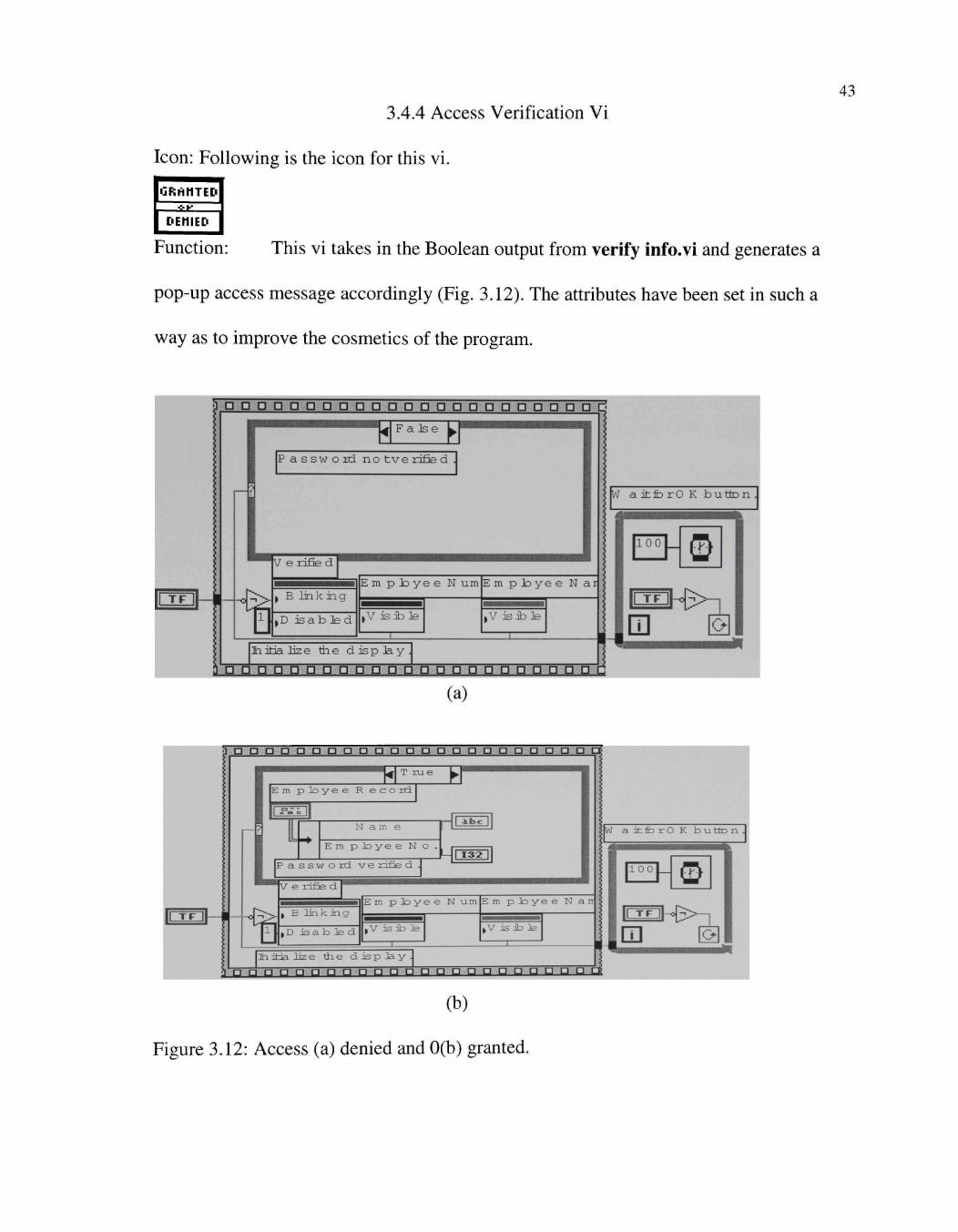
43 3.4.4 Access Verification Vi
Icon: Following is the icon for this vi.
SHHTED
Function: This vi takes in the Boolean output from verify info.vi and generates a
pop-up access message accordingly (Fig. 3.12). The attributes have been set in such a
way as to improve the cosmetics of the program.
D D D a a a Q D a o D a a a o a o a D a o D Q F a ]se I
P a s s w o r d n o t v e riSe d .
; W a i t f c rO K b u t t o n .
Em p l o y e e Num
jV i s ib ]e
E m p 3D y e e N a r
iV is ib ]e
i
F°]- S
m o I i i t i a l i ze the d i s p l a y :u^w^ Q a o d
(a)
(b)
Figure 3.12: Access (a) denied and 0(b) granted.
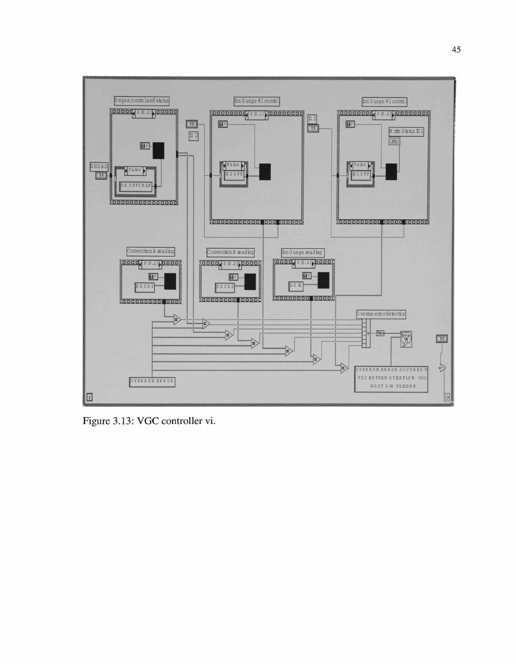
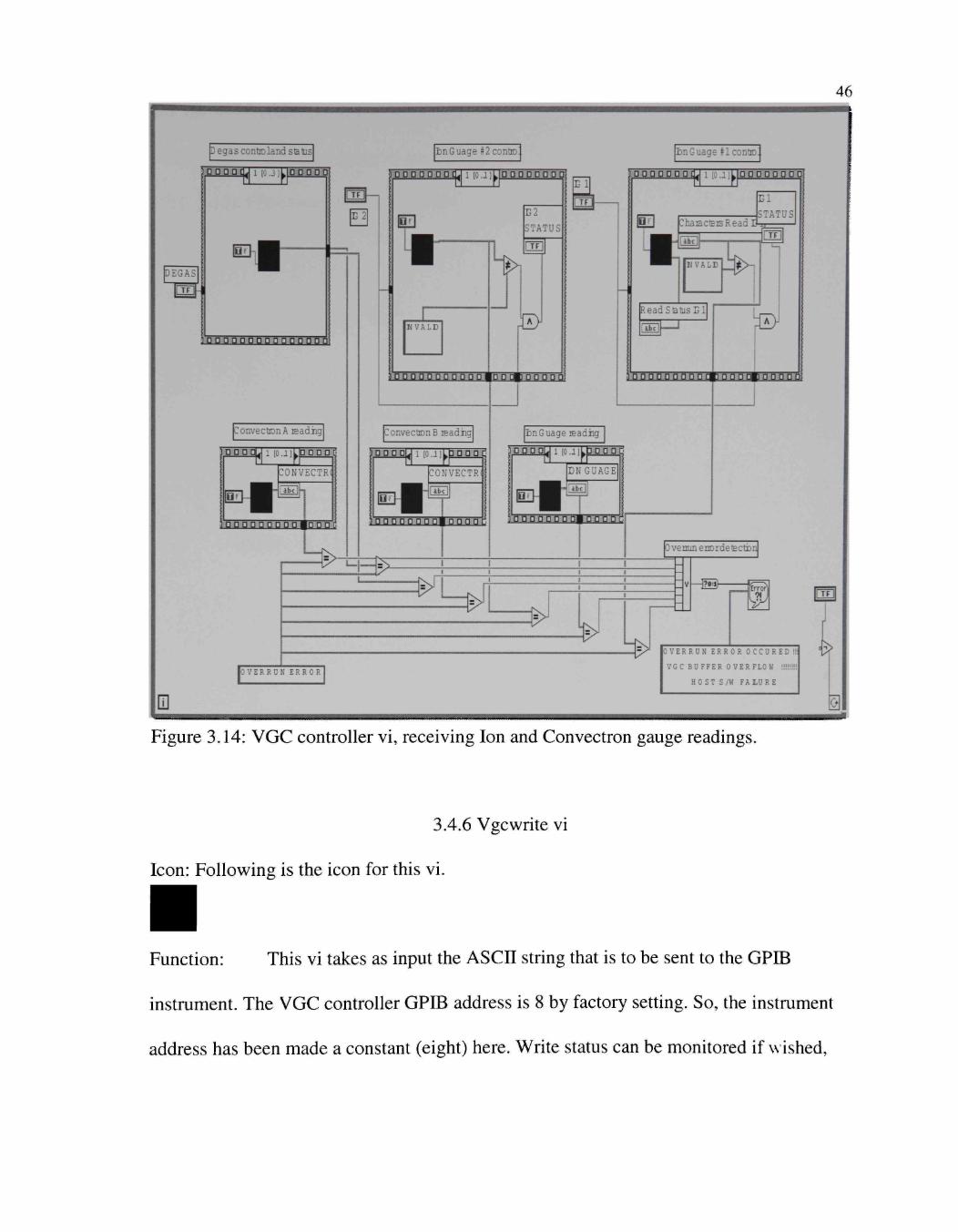
44 3.4.5 Vgc vi
Icon: Following is the icon for this vi.
Function: This vi executes continuously unless pressing "Close Panel" on the front
panel stops the while loop. The three upper sequence structures take care of Degas
Control, IG2 and IGl, respectively. Figures 3.13 and 3.14 show two consecutive steps in
the program. The GPIB address of the VGC controller is 8. Depending on whether the
Degas switch is on or off, the message DGONCRLF or DGOFFCRLF is being sent to the
device. In the next step vgcread.vi is listening to the device and is determining whether
Degas is on or off. This status is being displayed on the front panel at the same time.
Alternate use of vgcread.vi and vgcwrite.vi enables the program to listen and talk to the
instrument (VGC controller, in this case), respectively. Similarly, IGl and IG2 are being
talked to and listened by the program via the GPIB bus using the ASCII vocabulary of the
VGC controller. The three sequences at the bottom take care of the Gauge readings which
are directly read-in as ASCII characters and displayed in the same format. Please refer to
Appendix B for the GPIB commands for VGC controller.
45
D egas controland status SnGuage f2contiD: Bn Guage 11 control
i O a P D a j n in iL aooDOi
ID I DEGASl : - - « . I , II
I iDG 0 FFCRI
yflOtiijDtmaDDaijtawa
ConvecttDnA Eadhg
DOD Cy I . ^p DO D
MB ID S C G 1
ii3iQ'g"a"fa"ij'a'i3"fa"iij'a''a'
l O V E R R U N E R R O R
0
QOODaDaiL|o 10 l lL
iU-o D O O D o a g
(iFalse k
..-.. , _ . | j E 2 0FF
E 1
; UU
5'faDijbflHHaflaai|Df]tyg-DTTTT
ConvectiDnB Eadhg
pgoDODac^
iH-0 [O.J •^^••,"^-^^y^,ttjf,ijjii,iTfgiji
W rilEStatusEl
yaflgasaaHaqbflflHtifiaBgg
LnGuage readhg
10 D a g 10 ..1 l ip nag's
iD S C G 2
P J - - ^
DDOOUo lo..llipOOPC
iB-pS E
d'D"D'0'oaDO|DODacl jgOQPCDODlgODDEC
r 0 veniin ermrdetEctfan
t I
P I i
t^ >
^
(
O V E R R U N E R R O R O C C U R E D !l
V G C B U F F E R O V E R F L O W !!!!!!!!
H 0 S T S /W FA L U R E
fe
<.'
Figure 3.13: VGC controller vi.
46
Degas controland status BnGuage 12 control SnGuage «lconliD^
nag at^ i ioj|> oDoao
m m
E 2
illDOQDDDaonODDod
Convection A leadrig
ijg P 0 C « 1 10.11 ..0.0.0.0 C '
I D ^
CONVECTRl::
: ik< | k
s o f l D D a o n o a B f l c O G
r - ^
0 0 g d D D p I 110.11 ^ p g 0 p p g 0 0
in
- !
M V A L E
E2
STATUS
TF
iz>
J f D D o g g D O D O O D ^ D q g p D O O D d
E 1 Wl^ogoQgdJi fo nLlooDoaooD
'onvectoonB Kadhg
iDooou 1 iQ.nipnSo
CONVECTR(i
I—i HiiitlE]!
.a'a"a:ti:a'a"bb'|'d'aa'o'
^
jo'I ChaiactEisReadI
E l STATUS
Jbci i ! -
i ivALEi! ; ; ;^
ReadStatusEl
ILi
-&
j'flaBflBflaaatjiBflBHpatnnrl
BnGuage leadhg
ODogy 1 [u..iiLpoao
EN GUAGE
aaaatitiaaf dflBsa:
0 venun ertDrdetECtJon
¥ ^ = ^ \
¥ =$>
l O V E R R U N E R R O R
ID
O V E R R U N E R R O R O C C U R E D !
V G C BU F F E R O V E R F L O W !!!!!!:
H O S T S/W FA L U R E
m l
J
Figure 3.14: VGC controller vi, receiving Ion and Convectron gauge readings.
3.4.6 Vgcwrite vi
Icon: Following is the icon for this vi.
Function: This vi takes as input the ASCII string that is to be sent to the GPIB
instrument. The VGC controller GPIB address is 8 by factory setting. So, the instrument
address has been made a constant (eight) here. Write status can be monitored if w ished,
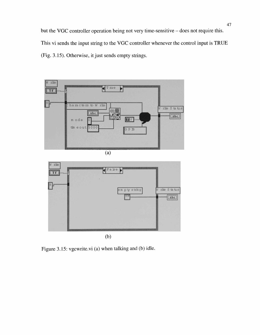
47 but the VGC controller operation being not very time-sensitive - does not require this.
This vi sends the input string to the VGC controller whenever the control input is TRUE
(Fig. 3.15). Otherwise, it just sends empty strings.
Iw rdtE
l ol—i Fa ]se I
em p ty s tnng
(b)
Figure 3.15: vgcwrite.vi (a) when talking and (b) idle.
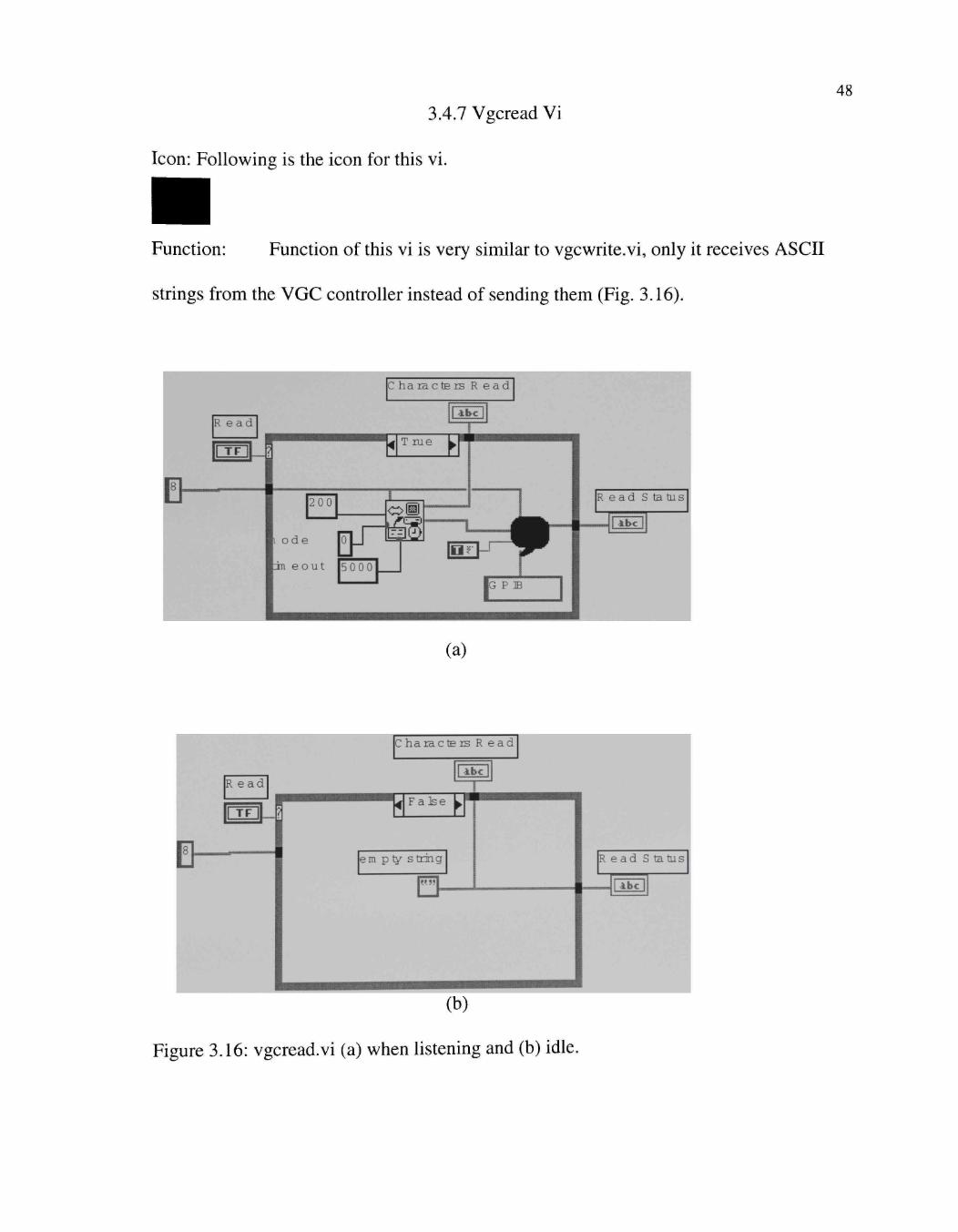
48 3.4.7 Vgcread Vi
Icon: Following is the icon for this vi.
Function: Function of this vi is very similar to vgcwrite.vi, only it receives ASCII
strings from the VGC controller instead of sending them (Fig. 3.16).
T rue
C h a r a c t E r s R e a d
5 0 0 0
(a)
C h a r a c t s r s R eaci
I Abe j
Fa] se
em p ty stnng
(b)
R e a d s ta tus
Figure 3.16: vgcread.vi (a) when listening and (b) idle.
CHAPTER 4
RESULTS AND SUMMARY
4.1 Data Acquisition From CCD
The imaging system is currently operational. But it has the severe limitation of
being slow. Under dark conditions, it can read in about 20 rows before the pixels start to
saturate from dark charges.
Figure 4.1: Oscilloscope trace of the raw analog signal out of the TC211 chip.
The oscilloscope trace in Figure 4.1 displays the analog raw image data heading towards saturation. The individual pixels cannot be discerned very clearly but the
49
50 tendency of sequential pixels under uniform illumination to increase in signal content is
apparent. The short horizontal trace at the right hand end of the curve represents the reset
voltage level of the amplifier at the CCD output. It may be noted here that the signal
shown appears to be negative going. This is due to this signal being the raw non-inverted
analog signal direct from the chip.
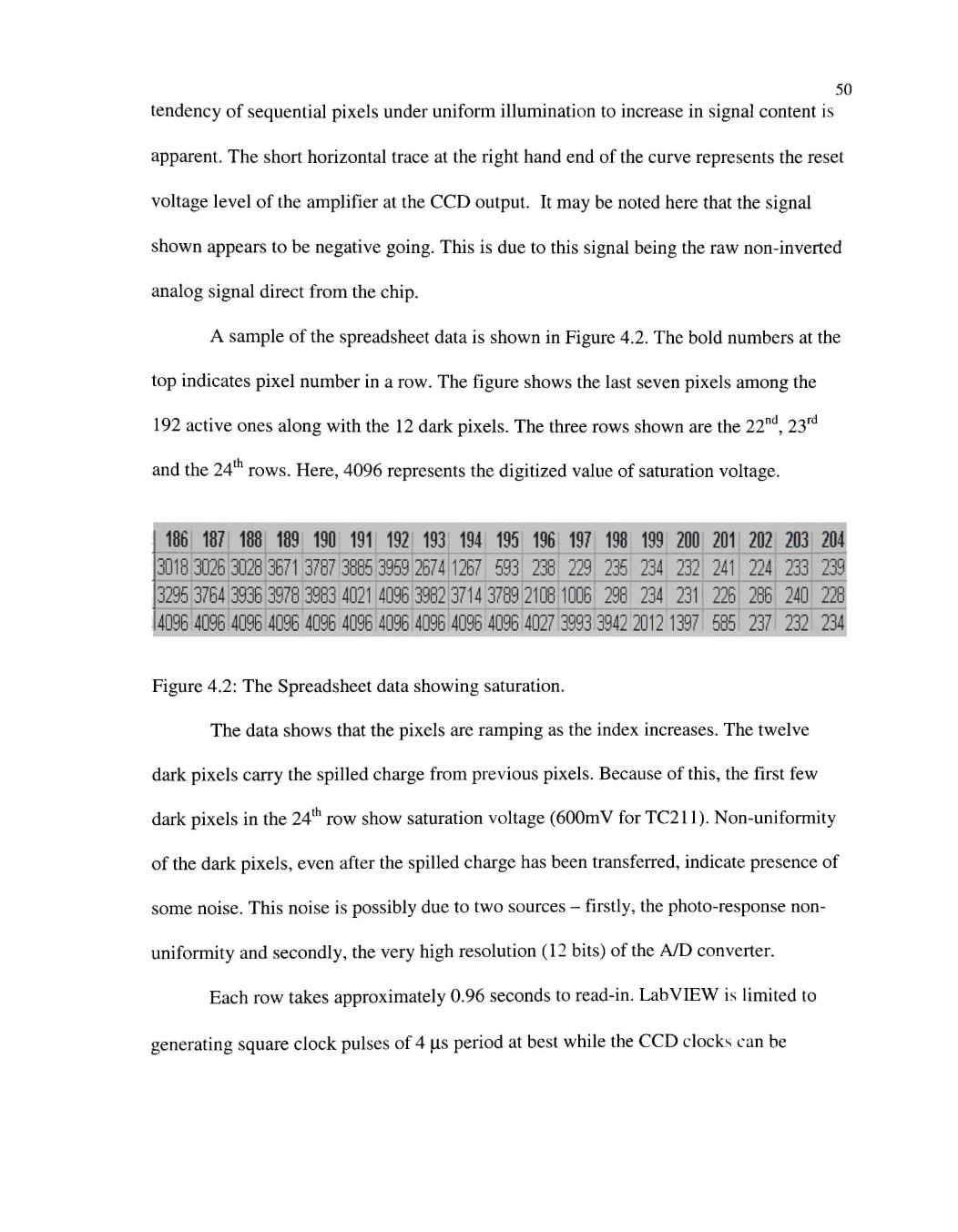
A sample of the spreadsheet data is shown in Figure 4.2. The bold numbers at the
top indicates pixel number in a row. The figure shows the last seven pixels among the
192 active ones along with the 12 dark pixels. The three rows shown are the 22"'', 23''
and the 24 rows. Here, 4096 represents the digitized value of saturation voltage.
186JJ87 J 8 8 ^ 1 8 9 1 % 191 192 193 194 195, 196 197 198 199 200 201. 202 203 204 30181302613028'3671 ^3787 3885 3959 •267411267^^ 329513764 3936 3978 3983 40214096 3982:3714 3789 21081006 298
234 234
232! 241 224 233 231 226^ 286' 240
239
P640%,|Qgy096:4096.4Q964Q96^4Q964096:4096.4027.3993.3942;2Q12 585. 237: 232 234
Figure 4.2: The Spreadsheet data showing saturation.
The data shows that the pixels are ramping as the index increases. The twelve
dark pixels carry the spilled charge from previous pixels. Because of this, the first few
dark pixels in the 24* row show saturation voltage (600mV for TC211). Non-uniformity
of the dark pixels, even after the spilled charge has been transferred, indicate presence of
some noise. This noise is possibly due to two sources - firstly, the photo-response non-
uniformity and secondly, the very high resolution (12 bits) of the A/D converter.
Each row takes approximately 0.96 seconds to read-in. LabVIEW is limited to
generating square clock pulses of 4 |Lts period at best while the CCD clocks can be

5:
operated at MHz level (SRG at 10 MHz and lAG at 1.5 MHz). The specified pulse
width of around 370 ns is quite unattainable with the on-board oscillator of AT-MIO-
16H9 and LabVIEW version 4.0. There definitely remain ways to make the program
work faster, but not anywhere near what the CCD can achieve in terms of speed. The
timing can be reduced only a little more. Though the system is not practical regarding
timing but it is fully working and acquiring data correctly.
4.2 Sputtering Equipment Control Svstem
The main control panel and the VGC control panel of this control software are
complete and these are working properly. The enhancements needed to make the other
subsystems work can be added to the existing program very easily.
REFERENCES
Berry, Richard and Kanto, Veikko and Munger, John. The CCD Camera Cookbook, Richmond, Virginia: Willman-Bell, Inc., 1994.
Hynecek, Jaroslav. "High-Resolution 8mm CCD Image Sensor with Correlated Clamp Sample and Hold Charge Detection Circuit." IEEE Transactions on Electron Devices, Vol. ED-33, No. 6, June 1986.
LabVIEW 4.0 Function Reference Manual National Instruments, 1996.
LabVIEW 5.1 Function Reference Manual, National Instruments, 1998.
TC211 Timing of Full Frame CCD Image Sensor, Texas Instruments, Inc. Application Note, June 1996.
TC211 192- X 165-Pixel CCD Image Sensor, Texas Instruments, Inc. Data Sheet, January 1990.
TC211 Timing of Full Frame CCD Image Sensor, Texas Instruments, Inc. Application Note, June 1996.
TC245 786- x 488- Pixel CCD Image Sensor, Texas Instruments, Inc. Data Sheet, December 1991.
Theuwissen, Albert J. P., Solid-State Imaging With Charge-Coupled Devices, Dordrecht, The Netherlands: Kluwer Academic Publishers, 1996.
52

APPENDIX A
PIN CONNECTION AND SIGNAL FOR THE CCD DATA ACQUISITION PROJECT
53
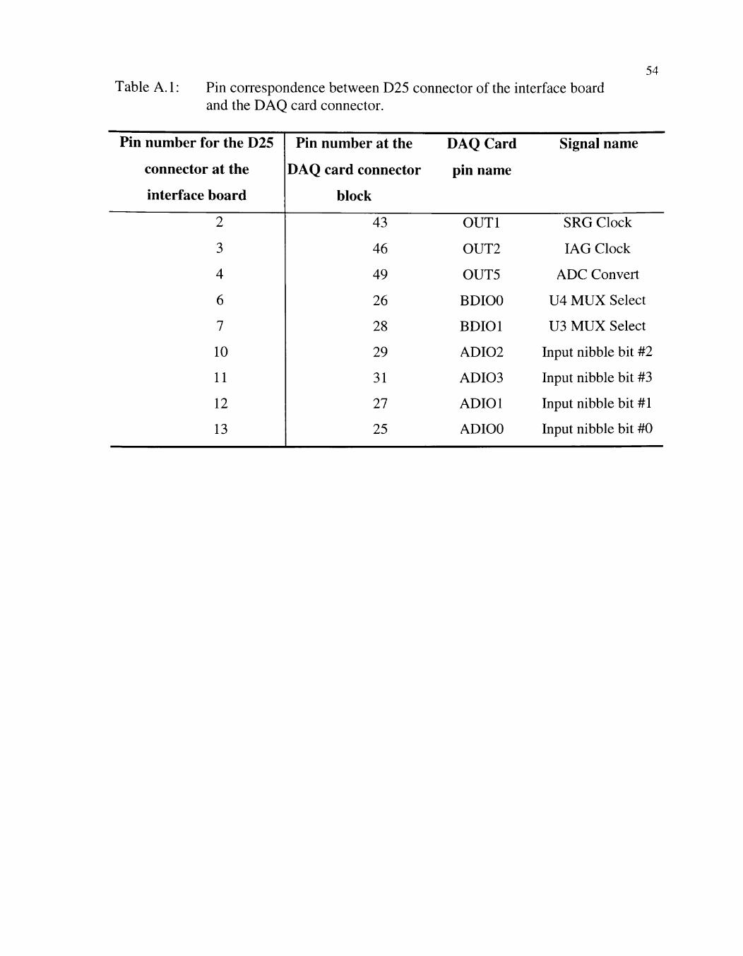
54 Table A. 1: Pin correspondence between D25 connector of the interface board
and the DAQ card connector.
Pin number for the D25
connector at the
interface board
2
3
4
6
7
10
11
12
13
Pin number at the
DAQ card connector
block
43
46
49
26
28
29
31
27
25
DAQ Card
pin name
OUTl
OUT2
OUT5
BDIOO
BDIOl
ADI02
ADI03
ADIOl
ADIOO
Signal name
SRG Clock
lAG Clock
ADC Convert
U4 MUX Select
U3 MUX Select
Input nibble bit #2
Input nibble bit #3
Input nibble bit #1
Input nibble bit #0
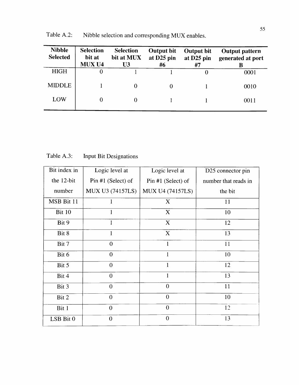
Table A.2: Nibble selection and corresponding MUX enables. 55
Nibble Selected
HIGH
MIDDLE
LOW
Selection bit at
MUXU4 0
1
0
Selection bit at MUX
U3 1
0
0
Output bit at D25 pin
#6 1
0
1
Output atD25
#7
bit pin
0
1
1
Output pattern generated at port
B 0001
0010
0011
Table A.3: Input Bit Designations
Bit index in
the 12-bit
number
MSB Bit 11
Bit 10
Bit 9
Bit 8
Bit 7
Bit 6
Bit 5
Bit 4
Bit 3
Bit 2
Bit 1
LSB Bit 0
Logic level at
Pin #1 (Select) of
MUXU3(74157LS)
1
1
1
1
0
0
0
0
0
0
0
0
Logic level at
Pin #1 (Select) of
MUXU4(74157LS)
X
X
X
X
1
1
1
1
0
0
0
0
D25 connector pin
number that reads in
the bit
11
10
12
13
11
10
12
13
11
10
12
13

APPENDIX B
THE SPUTTERING EQUIPMENT CONTROL
56
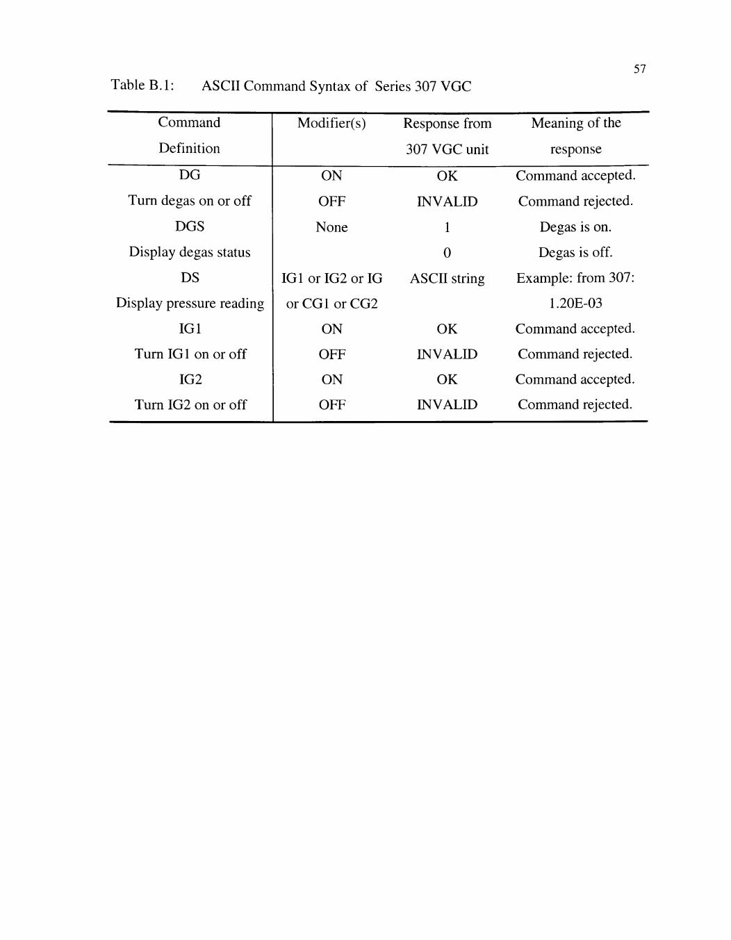
Table B.l: ASCII Command Syntax of Series 307 VGC 57
Command
Definition
DG
Turn degas on or off
DGS
Display degas status
DS
Display pressure reading
IGl
Turn IGl on or off
IG2
Turn IG2 on or off
Modifier(s)
ON
OFF
None
IGlorIG2orIG
orCGlorCG2
ON
OFF
ON
OFF
Response from
307 VGC unit
OK
INVALID
1
0
ASCII string
OK
INVALID
OK
INVALID
Meaning of the
response
Command accepted.
Command rejected.
Degas is on.
Degas is off.
Example: from 307:
1.20E-03
Command accepted.
Command rejected.
Command accepted.
Command rejected.

PERMISSION TO COPY
In presenting this thesis in partial fulfillment of the requirements for a
master's degree at Texas Tech University or Texas Tech University Health Sciences
Center, I agree that the Library and my major department shall make it freely
available for research purposes. Permission to copy this thesis for scholarly
purposes may be granted by the Director of the Library or my major professor.
It is understood that any copying or publication of this thesis for financial gain
shall not be allowed without my further written permission and that any user
may be liable for copyright infringement.
Agree (Permission is granted.)
Student's Signature Date
Disagree (Permission is not granted.)
Student's Signature Date