Embed Size (px)
Citation preview
Interface Synthesis using Memory Mapping
for an FPGA Platform
Manev Luthra‡ Sumit Gupta‡ Nikil Dutt‡ Rajesh Gupta§ Alex Nicolau‡
CECSTechnical Report #03-20
June 2003
Center for Embedded Computer Systems‡ School of Information and Computer Science § Dept. of Computer Science and Engineering
University of California at Irvine University of California at San Diego�mluthra, sumitg, dutt, nicolau � @cecs.uci.edu [email protected]
http://www.cecs.uci.edu/ � spark
Abstract
Several system-on-chip (SoC) platforms have recently emerged that use reconfigurable logic (FPGAs) as a pro-
grammable co-processor to reduce the computational load on the main processor core. We present an interface
synthesis approach that enables us to do hardware-software codesign for such FPGA-based platforms. The ap-
proach is based on a novel memory mapping algorithm that maps data used by both the hardware and the software
to shared memories on the reconfigurable fabric. The memory mapping algorithm uses scheduling information
from a high-level synthesis tool to map variables, arrays and complex data structures to the shared memories in
a way that minimizes the number of registers and multiplexers used in the hardware interface. We also present
three software schemes that enable the application software to communicate with this hardware interface. We
demonstrate the utility of our approach and study the trade-offs involved using a case study of the co-design of a
computationally expensive portion of the MPEG-1 multimedia application on to the Altera Nios platform.
Contents
1 Introduction 4
2 Related Work 5
3 Role of Interface Synthesis and Memory Mapping in a Co-Design Methodology 5
3.1 Memory Mapping . . . . . . . . . . . . . . . . . . . . . . . . . . . . . . . . . . . . . . . . . . . . . . . . . 6
3.2 Problem Formulation . . . . . . . . . . . . . . . . . . . . . . . . . . . . . . . . . . . . . . . . . . . . . . . 7
3.3 Mapping Algorithm . . . . . . . . . . . . . . . . . . . . . . . . . . . . . . . . . . . . . . . . . . . . . . . . 8
3.4 Construction of Conflict Graphs . . . . . . . . . . . . . . . . . . . . . . . . . . . . . . . . . . . . . . . . . 9
4 The Hardware Interface Architecture 12
5 The SW Interface 12
5.1 Data Transfer Based Scheme . . . . . . . . . . . . . . . . . . . . . . . . . . . . . . . . . . . . . . . . . . . 13
5.2 Shared Memory Based Schemes . . . . . . . . . . . . . . . . . . . . . . . . . . . . . . . . . . . . . . . . . 13
6 Experimental Setup and Results 14
6.1 Case Study: MPEG-1 Prediction Block . . . . . . . . . . . . . . . . . . . . . . . . . . . . . . . . . . . . . 15
7 Conclusions and Future Work 18
2
List of Figures
1 Role of interface synthesis in a co-design methodology . . . . . . . . . . . . . . . . . . . . . . . . . . . . . 6
2 The advantages of memory mapping . . . . . . . . . . . . . . . . . . . . . . . . . . . . . . . . . . . . . . . 7
3 The memory mapping algorithm . . . . . . . . . . . . . . . . . . . . . . . . . . . . . . . . . . . . . . . . . 9
4 Determining the list of available memories . . . . . . . . . . . . . . . . . . . . . . . . . . . . . . . . . . . . 10
5 Construction of conflict graphs . . . . . . . . . . . . . . . . . . . . . . . . . . . . . . . . . . . . . . . . . . 11
6 The hardware interface architecture . . . . . . . . . . . . . . . . . . . . . . . . . . . . . . . . . . . . . . . 12
7 Modified address offsets in the software interface after memory mapping . . . . . . . . . . . . . . . . . . . . 13
8 The Nios embedded system . . . . . . . . . . . . . . . . . . . . . . . . . . . . . . . . . . . . . . . . . . . . 14
9 Execution times for different hardware software partitions of the application . . . . . . . . . . . . . . . . . . 18
List of Tables
1 Logic synthesis results for the target FPGA . . . . . . . . . . . . . . . . . . . . . . . . . . . . . . . . . . . 16
2 Execution times of various kernels of the application . . . . . . . . . . . . . . . . . . . . . . . . . . . . . . 17
3
1 Introduction
Platform based designs provide promising solutions for handling the growing complexity of chip designs [1].
FPGAs often play an important role in platforms by providing flexible, reconfigurable circuit fabrics to build and
optimize target applications.
Our focus is on platform designs for multimedia and image processing applications. Our target architecture
models many emerging platforms that contain a general purpose processor assisted by dedicated hardware for
computationally intensive tasks. The hardware assists are implemented on-board FPGA blocks and thus, can be
programmed for different applications. Binding the application functionality to software and hardware requires
automated methods to specify, generate and optimize the interface between them. The interface should be fast,
transparent and require minimal hardware and software resources. This report presents a methodology to generate
these interfaces.
Multimedia and image processing applications typically operate on a large data set. Consequently, when these
applications are partitioned and mapped onto an FPGA-based platform, this data has to be communicated and
shared between the hardware and software components. Configurable logic blocks in FPGAs are typically ineffi-
cient for use as memories: if we store each data element in a register and provide an independent access mechanism
for each one, then the resulting memory implementation occupies a large portion of the FPGA fabric. Instead, an
efficient way to implement these large memories is to cluster the data elements into RAMs or register banks. In
this report, we present our interface synthesis approach that efficiently utilizes embedded RAMs in FPGAs to im-
plement the memory. Our approach is based on a novel memory mapping algorithm that generates and optimizes a
hardware interface used for integrating the computationally expensive application kernels (hardware assists) with
the rest of the platform.
Our memory mapping algorithm makes use of scheduling information on per cycle data access patterns (avail-
able from the high-level synthesis tool) in order to map registers to memories. The unique feature of this algorithm
is its ability to efficiently handle designs in which data access patterns are unknown during scheduling - for exam-
ple, an array being indexed by variable indices which become known only at run-time. This feature proves to be
extremely useful when dealing with designs involving control flow.
To validate our co-design methodology, we present a case study of the co-design of a computationally expensive
portion of the MPEG-1 multimedia application. We find that without using our memory mapping algorithm, the
portion mapped to the FPGA is too big to fit inside it. We also compare results for various hardware-software
interfacing schemes used with this design.
The rest of this report is organized as follows: in the next section, we discuss related work. In Section 3,
4
we describe our methodology and the relation between memory mapping and hardware interface synthesis. We
also formulate the memory mapping problem and present an algorithm for solving it. In Section 4 we describe
the architecture of our hardware interface. In Section 5, we describe the changes required in the software to use
the hardware interface and explain three hardware-software interfacing schemes. In Section 6, we describe our
MPEG-1 case study and then, conclude the report with a discussion.
2 Related Work
Hardware-software partitioning [2, 3] and high level synthesis [4, 5] have received significant attention over
the past decade. Interface synthesis techniques have focused on various issues like optimizing the use of external
IO pins of micro-controllers and minimizing glue logic [6]. However, the use of memory mapping for interface
synthesis has not been considered. Furthermore, hardware-software co-design methodologies that synthesize the
hardware component as an ASIC, pay little attention towards optimizing the memory mapping since the amount
of logic that can be mapped to an ASIC is less severely constrained than that for FPGAs [2, 7, 8].
Most previous work on memory mapping and allocation of multiport memories has been done in the context
of data path synthesis and has focused on purely data flow designs (no control constructs) [9, 10, 11]. These
algorithms do not deal with unknown data access patterns because no control flow is involved. Memory mapping
and register binding algorithms in the data path synthesis domain are based on variable lifetime analysis and
register allocation heuristics [10, 12, 13].
Early work on memory mapping in the context of FPGAs has not utilized scheduling information [12, 14].
Karchmer and Rose present an algorithm for packing data structures with different aspect ratios into fixed width
memories available on FPGAs [15]. However, this is of limited use when applications use simple and regular data
structures.
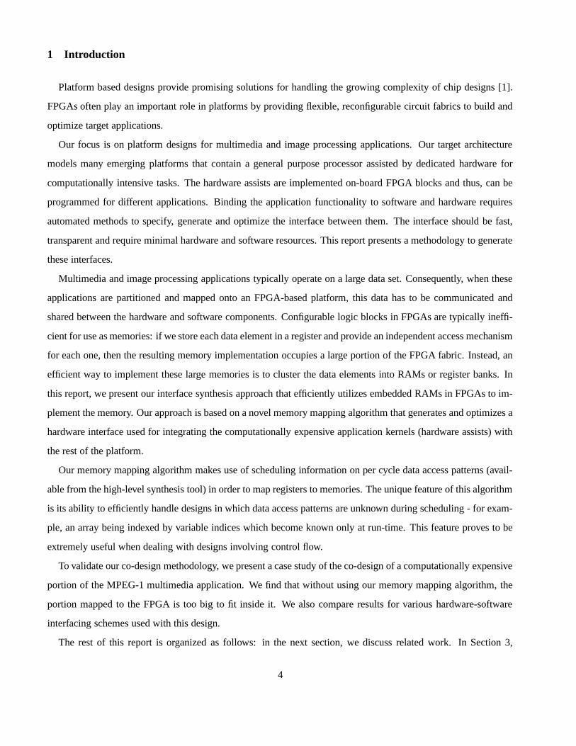
3 Role of Interface Synthesis and Memory Mapping in a Co-Design Methodology
Interface synthesis is an important aspect of our hardware-software co-design methodology, as shown in Figure
1. In our approach, we rely on a C/C++ based description [16, 17, 18] for the system model. After hardware-
software partitioning, the hardware part is scheduled using a high-level synthesis tool and the scheduling informa-
tion is passed to the interface synthesizer.
This interface synthesizer – described in detail in the rest of the report – generates the hardware interface and
re-instruments the software component of the application to make appropriate calls to the hardware component
via this interface. It also passes the addresses of all registers that have been mapped to memories in the hardware
interface to the high-level synthesis tool.
5
Code GenerationAssembly/Machine
and P&RLogic Synthesis
CompilerSoftware
(with Interface)Behavioral C Synthesis
InterfaceSynthesis
High−Level
(Interface) (HW)VHDLRTLRTL
VHDL
Behavioral C(HW Part)
Behavioral C(SW Part)
PartitioningHW/SW
C/C++ VariantSystem Specification
Core
FPGA Based Platform
Processor
Peri−−pherals
I/O
FPGA
Figure 1. Role of interface synthesis in a co-design methodology
The RTL code generated by the high-level synthesis tool and the interface synthesizer are then downloaded to
the FPGA on the platform. Similarly, the software component is compiled and downloaded into the instruction
memory of the processor.
3.1 Memory Mapping
Multimedia and image processing applications process large amounts of data. After partitioning, the hardware
component has to operate on the same data that the software operates on. Thus, the hardware component needs to
store this data on the FPGA (see Section 4 for how this is achieved). Also, the stored data has to be multiplexed
and steered to various functional units that comprise the hardware component. The presence of control flow in the
application code also adds significantly to the multiplexing costs.
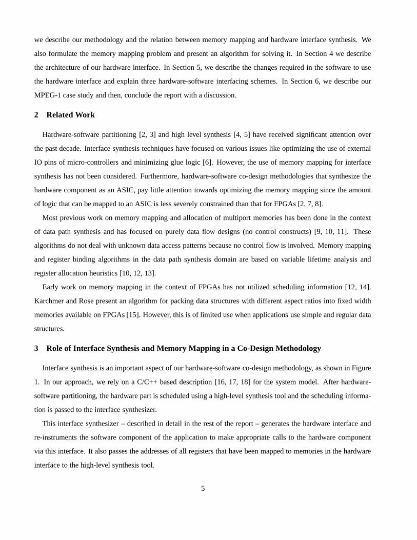
The way the data is mapped to the memory has a tremendous impact on the complexity of the multiplexers
and control generated. Ideally, we would store all data in a single large memory. However, such a memory
would require as many ports as the maximum number of simultaneous memory accesses in any cycle [11]. This is
impractical for programmable FPGA platforms, since they provide memories with only a limited number of ports
[19, 20]. Consequently, memories with a larger number of ports have to be implemented using individual registers.
This requires a large number of registers and complex, large multiplexers as shown in Figure 2(a).
In our memory mapping approach, we utilize scheduling information – available from the high-level synthesis
6
Unit 1Functional Functional Unit M
Functional Unit MFunctional Unit 1
1P Ports P Ports2 P Portsk
Mem 1 Mem 2 Mem k
1 Port 1 Port 1 Port
Elem 1 Elem 2 Elem 3
1 Port
Elem N
K : 2M Mux
(b)
(a)
N : 2M Mux
Elem 2Elem N Elem 3
Elem 1
Figure 2. (a) Unmapped Design: Registers for each data element (b) Mapped Design: Data elements mapped to
memories, K � N
tool – about data accesses and the cycles that they occur in. We can then map the data elements to memory banks,
given constraints on the maximum number of ports each memory in the target FPGA can have. This approach
eliminates the use of registers for storage, thus, saving a large amount of area, which in turn can be used for the
application logic. This way, we can also use much smaller and faster multiplexers in the data-path as illustrated in
Figure 2(b). In this figure, size � Mem1 ��� size � Mem2 ������������ size � Memk �� N.
Arrays and data structures are mapped to memories after being broken down into their basic constituents (vari-
ables). These can then be mapped in a way identical to regular variables. Consequently, these basic constituents
might get mapped to non-contiguous memory addresses/locations. In Section 5 we show how this drawback can
easily be overcome by making a few changes to the application software.
3.2 Problem Formulation
We are given a set of n variables, V � vi; i 1 � 2 � ������� � n � that are accessed (read and written) by all the kernels
of the application. In our current model, only one kernel executes at any given time. This implies that contention
for variable accesses between two kernels can never occur. Note that, each element in an array or data structure is
considered as a distinct variable vi in V ; so for example, an array of size n will have n entries in V . We are also
given a set of memory resource types, Mtype �� m j; j � Z ��� where the subscript j indicates the maximum number
of ports available. The number of read ports of memory type m j are given by Portsread � m j � and write ports by
Portswrite � m j � .
7
Definition 3.1 The memory mapping problem is to find a memory allocation φ : � Mtypes � Z � � � V that is a
mapping of memory instances to variables assigned to them in the design. This mapping also gives the list M
of all the memory instances allocated to the design. φ � m j � n � represents the list of variables mapped to the n-th
instance of memory type m j. The optimization problem is to minimize the total number of memory instances,
given by size � M � , with the constraint that for each memory instance � m j � n � used in the design, the number of
simultaneous accesses during any cycle should not exceed the number of memory ports available on m j.
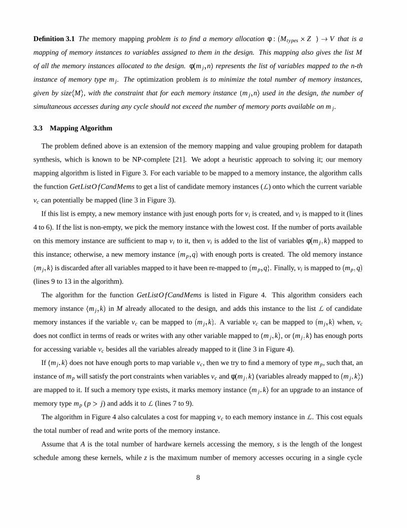
3.3 Mapping Algorithm
The problem defined above is an extension of the memory mapping and value grouping problem for datapath
synthesis, which is known to be NP-complete [21]. We adopt a heuristic approach to solving it; our memory
mapping algorithm is listed in Figure 3. For each variable to be mapped to a memory instance, the algorithm calls
the function GetListO fCandMems to get a list of candidate memory instances (L) onto which the current variable
vc can potentially be mapped (line 3 in Figure 3).
If this list is empty, a new memory instance with just enough ports for vi is created, and vi is mapped to it (lines
4 to 6). If the list is non-empty, we pick the memory instance with the lowest cost. If the number of ports available
on this memory instance are sufficient to map vi to it, then vi is added to the list of variables φ � m j � k � mapped to
this instance; otherwise, a new memory instance � mp � q � with enough ports is created. The old memory instance
� m j � k � is discarded after all variables mapped to it have been re-mapped to � m p � q � . Finally, vi is mapped to � mp � q �(lines 9 to 13 in the algorithm).
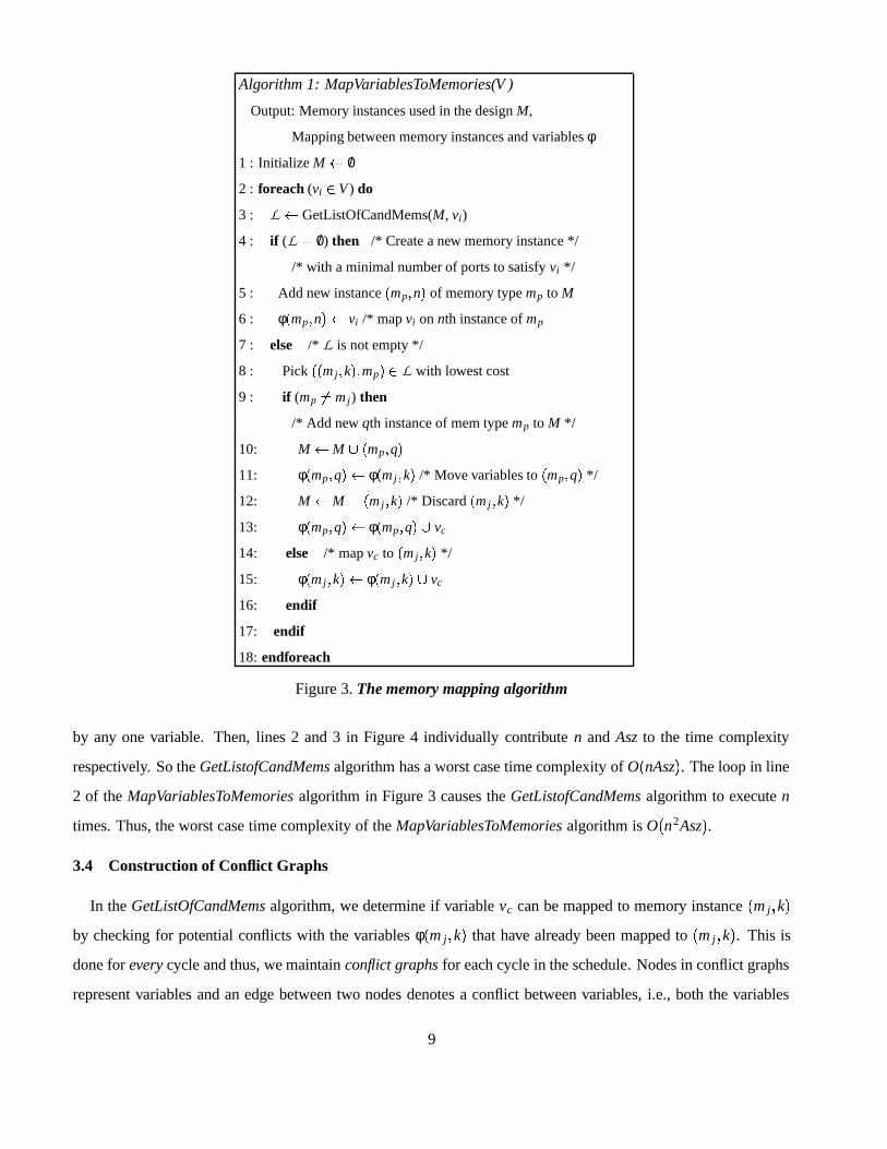
The algorithm for the function GetListO fCandMems is listed in Figure 4. This algorithm considers each
memory instance � m j � k � in M already allocated to the design, and adds this instance to the list L of candidate
memory instances if the variable vc can be mapped to � m j � k � . A variable vc can be mapped to � m j � k � when, vc
does not conflict in terms of reads or writes with any other variable mapped to � m j � k � , or � m j � k � has enough ports
for accessing variable vc besides all the variables already mapped to it (line 3 in Figure 4).
If � m j � k � does not have enough ports to map variable vc, then we try to find a memory of type mp, such that, an
instance of mp will satisfy the port constraints when variables vc and φ � m j � k � (variables already mapped to � m j � k � )are mapped to it. If such a memory type exists, it marks memory instance � m j � k � for an upgrade to an instance of
memory type mp (p � j) and adds it to L (lines 7 to 9).
The algorithm in Figure 4 also calculates a cost for mapping vc to each memory instance in L . This cost equals
the total number of read and write ports of the memory instance.
Assume that A is the total number of hardware kernels accessing the memory, s is the length of the longest
schedule among these kernels, while z is the maximum number of memory accesses occuring in a single cycle
8
Algorithm 1: MapVariablesToMemories(V )
Output: Memory instances used in the design M,
Mapping between memory instances and variables φ
1 : Initialize M � /0
2 : foreach (vi� V ) do
3 : L � GetListOfCandMems(M, vi)
4 : if (L � /0) then /* Create a new memory instance */
/* with a minimal number of ports to satisfy vi */
5 : Add new instance � mp � n � of memory type mp to M
6 : φ � mp � n ��� vi /* map vi on nth instance of mp
7 : else /* L is not empty */
8 : Pick ��� m j � k � � mp � � L with lowest cost
9 : if (mp �� m j) then
/* Add new qth instance of mem type mp to M */
10: M � M � mp � q �11: φ � mp � q ��� φ � m j � k � /* Move variables to � mp � q � */
12: M � M ��� m j � k � /* Discard � m j � k � */
13: φ � mp � q ��� φ � mp � q � vc
14: else /* map vc to � m j � k � */
15: φ � m j � k ��� φ � m j � k �� vc
16: endif
17: endif
18: endforeach
Figure 3. The memory mapping algorithm
by any one variable. Then, lines 2 and 3 in Figure 4 individually contribute n and Asz to the time complexity
respectively. So the GetListofCandMems algorithm has a worst case time complexity of O � nAsz � . The loop in line
2 of the MapVariablesToMemories algorithm in Figure 3 causes the GetListofCandMems algorithm to execute n
times. Thus, the worst case time complexity of the MapVariablesToMemories algorithm is O � n2Asz � .
3.4 Construction of Conflict Graphs
In the GetListOfCandMems algorithm, we determine if variable vc can be mapped to memory instance � m j � k �by checking for potential conflicts with the variables φ � m j � k � that have already been mapped to � m j � k � . This is
done for every cycle and thus, we maintain conflict graphs for each cycle in the schedule. Nodes in conflict graphs
represent variables and an edge between two nodes denotes a conflict between variables, i.e., both the variables
9
Algorithm 2: GetListOfCandMems(M, vc)
Return: Available Memories List L
1 : Initialize List L � /0
2 : foreach (memory instance � m j � k � � M) do
3 : if (vc does not conflict with φ � m j � k � in any cycle)
or ( � m j � k � has enough ports to map vc) then
4 : L � L � � m j � k � � m j ���5 : Cost � m j � k ��� Portsread � m j � �
Portswrite � m j �6 : else /*either conflict or insufficient ports in � m j � k � */
7 : if (there exists mp�
Mtype with enough ports
8 : to map all variables from � m j � k � and vc) then
9 : L � L ��� m j � k � � mp ���10: Cost � m j � k � � Portsread � mp � �
Portswrite � mp �11: endif
12: endif
13: endforeach
Figure 4. Determining the list of available memories
are accessed in that cycle.
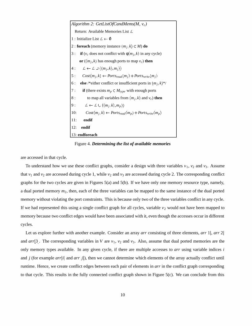
To understand how we use these conflict graphs, consider a design with three variables v1, v2 and v3. Assume
that v1 and v2 are accessed during cycle 1, while v2 and v3 are accessed during cycle 2. The corresponding conflict
graphs for the two cycles are given in Figures 5(a) and 5(b). If we have only one memory resource type, namely,
a dual ported memory m2, then, each of the three variables can be mapped to the same instance of the dual ported
memory without violating the port constraints. This is because only two of the three variables conflict in any cycle.
If we had represented this using a single conflict graph for all cycles, variable v2 would not have been mapped to
memory because two conflict edges would have been associated with it, even though the accesses occur in different
cycles.
Let us explore further with another example. Consider an array arr consisting of three elements, arr � 1 � , arr � 2 �and arr � 3 � . The corresponding variables in V are v1, v2 and v3. Also, assume that dual ported memories are the
only memory types available. In any given cycle, if there are multiple accesses to arr using variable indices i
and j (for example arr � i � and arr � j � ), then we cannot determine which elements of the array actually conflict until
runtime. Hence, we create conflict edges between each pair of elements in arr in the conflict graph corresponding
to that cycle. This results in the fully connected conflict graph shown in Figure 5(c). We can conclude from this
10
V1 V
V
3
2
V1 V
V2
3 V1 V
V2
3V1 V
V2
3
(a) Cycle 1 (b) Cycle 2 (c) Plain Nodes (d) Colored Nodes
Figure 5. (a) Conflict graph for cycle 1 (b) Conflict graph for cycle 2 (c) Conflict graph with colorless nodes (d)
Conflict graph with multi-colored nodes
conflict graph that none of the three variables can be mapped to the same memory instance since the memory has
only two ports.
But, this is an incorrect conclusion because only two of the three variables will be accessed in any cycle. This
implies that the three variables can be mapped to a dual ported memory. Thus, we find that per cycle conflict
graphs are, by themselves, not powerful enough to capture all the information necessary to perform effective
memory mapping.
To address such issues, we introduce the notion of accumulating colors in the nodes of the conflict graphs of
each cycle. From among a group of variables VG, if access of any one in a cycle rules out access of the rest in
that cycle, then the nodes corresponding to each variable in the group VG are marked with the same color cG. This
color is unique from that of all other groups. A node can accumulate colors by being a member of more than one
such group.
Applying this to our example, we get the conflict graph depicted in Figure 5(d). v1, v2 and v3 form a group
corresponding to access by arr � i � . Each of these three variables are marked with one color since accessing any
one of them rules out accessing the other two. Similarly, v1, v2 and v3 form another group corresponding to access
by arr � j � and are marked with a second color. Thus, each of the three nodes/variables end up accumulating two
colors.
The number of ports needed to map a set of variables to a single memory instance, is equal to the maximum
number of colors in any cycle of all the variables being mapped to that memory instance. In our example, the
number of colors accumulated by v1, v2 and v3 is two. Thus, we can safely map these three variables to a dual
ported memory. We use this coloring technique while creating the per cycle conflict graphs used by our memory
mapping algorithm.
11
mP1
Memory
Controller
PortsCPUBus
LogicBlock 1
PortsL
App. 1
Logic
La Ports
Control
App.LogicBlock a
Mapped Memory (M)
Ports
Ports
P1
P2
Pk
m
m
P2
Pk
InterfaceBus 1 Port
ProcessorCore FPGA
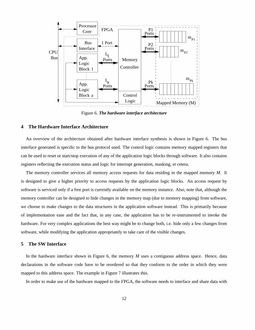
Figure 6. The hardware interface architecture
4 The Hardware Interface Architecture
An overview of the architecture obtained after hardware interface synthesis is shown in Figure 6. The bus
interface generated is specific to the bus protocol used. The control logic contains memory mapped registers that
can be used to reset or start/stop execution of any of the application logic blocks through software. It also contains
registers reflecting the execution status and logic for interrupt generation, masking, et cetera.
The memory controller services all memory access requests for data residing in the mapped memory M. It
is designed to give a higher priority to access requests by the application logic blocks. An access request by
software is serviced only if a free port is currently available on the memory instance. Also, note that, although the
memory controller can be designed to hide changes in the memory map (due to memory mapping) from software,
we choose to make changes to the data structures in the application software instead. This is primarily because
of implementation ease and the fact that, in any case, the application has to be re-instrumented to invoke the
hardware. For very complex applications the best way might be to change both, i.e. hide only a few changes from
software, while modifying the application appropriately to take care of the visible changes.
5 The SW Interface
In the hardware interface shown in Figure 6, the memory M uses a contiguous address space. Hence, data
declarations in the software code have to be reordered so that they conform to the order in which they were
mapped to this address space. The example in Figure 7 illustrates this.
In order to make use of the hardware mapped to the FPGA, the software needs to interface and share data with
12
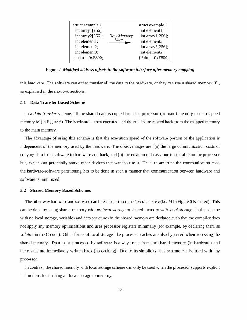
int array1[256]; int array2[256]; int array1[256]; int element1; int element2; int element3;
int element1;
int element3; int array2[256]; int element2;
MapNew Memory
} *dm = 0xF800; } *dm = 0xF800;
struct example { struct example {
Figure 7. Modified address offsets in the software interface after memory mapping
this hardware. The software can either transfer all the data to the hardware, or they can use a shared memory [8],
as explained in the next two sections.
5.1 Data Transfer Based Scheme
In a data transfer scheme, all the shared data is copied from the processor (or main) memory to the mapped
memory M (in Figure 6). The hardware is then executed and the results are moved back from the mapped memory
to the main memory.
The advantage of using this scheme is that the execution speed of the software portion of the application is
independent of the memory used by the hardware. The disadvantages are: (a) the large communication costs of
copying data from software to hardware and back, and (b) the creation of heavy bursts of traffic on the processor
bus, which can potentially starve other devices that want to use it. Thus, to amortize the communication cost,
the hardware-software partitioning has to be done in such a manner that communication between hardware and
software is minimized.
5.2 Shared Memory Based Schemes
The other way hardware and software can interface is through shared memory (i.e. M in Figure 6 is shared). This
can be done by using shared memory with no local storage or shared memory with local storage. In the scheme
with no local storage, variables and data structures in the shared memory are declared such that the compiler does
not apply any memory optimizations and uses processor registers minimally (for example, by declaring them as
volatile in the C code). Other forms of local storage like processor caches are also bypassed when accessing the
shared memory. Data to be processed by software is always read from the shared memory (in hardware) and
the results are immediately written back (no caching). Due to its simplicity, this scheme can be used with any
processor.
In contrast, the shared memory with local storage scheme can only be used when the processor supports explicit
instructions for flushing all local storage to memory.
13
Peripherals
MainMemory
Set ofExternal
MemoryController
External
PIO’s
UART’s
NiosEmbeddedProcessor
Timer
User-definedModule
Wrapper
User-defined for the
Module
Ava
lon
Bus
FPGA Fabric
Figure 8. The Nios embedded system
The clear advantage of both these schemes is the zero data transfer (communication) cost between software and
hardware. However, the shared memory with no local storage scheme has the additional advantage that it maintains
data coherency since the data is not buffered inside the processor’s local memory. But, this causes extra traffic on
the processor bus whenever the software portion of the application is running. A disadvantage of both schemes is
that a larger access time for mapped memory can degrade performance significantly. Thus, the performance with
these schemes depends critically on the speed of the processor bus, the mapped memory and associated access
logic.
6 Experimental Setup and Results
We used Altera’s Nios development platform [19] for implementing the system. This platform consists of a soft
core of the Nios embedded processor (no caches) to which various peripherals can be connected for customization.
Once the system has been customized, it can be synthesized and mapped onto an FPGA based board provided by
Altera. The user can use dedicated RAM block bits inside the FPGA to implement memories having two or fewer
ports. The system level architecture is shown in Figure 8 where the user-defined module is the hardware depicted
inside the FPGA in Figure 6. This entire system, consisting of the Nios processor and its standard peripherals, the
main memory, the CPU bus and the user-defined module operate at a frequency of 33.33 MHz.
We synthesized application kernels using a parallelizing high level synthesis framework called SPARK [4]. This
framework takes a behavioral description in C as input and generates synthesizable register-transfer level VHDL.
SPARK applies a set of compiler, parallelizing compiler, and synthesis transformations to optimize the overall
14
quality of the synthesized circuit, i.e., the circuit delay and area. The SPARK methodology is particularly useful
for designs with complex control flow.
The generated RTL VHDL was synthesized using the logic synthesis tool, Leonardo Spectrum; the resultant
netlist was mapped to the FPGA using the Altera Quartus tool. The portions of the application which were not
mapped to hardware were compiled and mapped onto the processor on the FPGA platform using the compiler
suite that is part of the Nios development toolkit.
6.1 Case Study: MPEG-1 Prediction Block
In this section, we present a case study using a multimedia application to evaluate the effectiveness of our
mapping algorithm and to study the trade-offs between the three interfacing and communication schemes described
in Section 5. We used the prediction block from the MPEG-1 multimedia application. The globals declared by
this block were 53 integer variables and two integer arrays of 64 entries each; making a total of 181 integer data
elements.
To begin with, three computationally intensive kernels in the application were identified using profiling in-
formation with the entire application running in software; each of these kernels consisted of nested loops with
identical structures. High level synthesis of this loop structure was performed using our synthesis tool followed
by the creation of a user-defined module consisting of the application logic for this loop structure, the memory
controller, control logic and the bus interface logic. The resource allocation used for this design during high level
synthesis was 1 ALU, 1 comparator and 1 shifter.
We used the Leonardo Spectrum logic synthesis tool to synthesize the user-defined module for the Altera FPGA.
The results of this synthesis are shown in Table 1. This table gives the area of the synthesized circuit in terms of
the logic cells, the maximum frequency that the synthesized hardware module can be executed at on the FPGA,
and the amount of memory required for the hardware module in terms of RAM block bits. The first row shows
synthesis results for the Nios system module without our user-defined module. The second row shows the results
for the user-defined module described earlier in this section. This hardware module was obtained without applying
our memory mapping technique. We could not integrate this design with the Nios embedded system because it
was too big to fit inside the FPGA, given that the capacity of the FPGA was 8320 Logic Cells (LCs). Note that
the maximum frequencies shown in Table 1 are only the estimates of the logic synthesis tool and were found to be
slightly conservative.
Next, we applied the memory mapping algorithm to the 181 data elements in the design and came up with a
new memory configuration. The constraint on the maximum number of ports per memory was set to two because
the target FPGA could at the most support dual ported RAMs. Then, we made a new memory controller based on
15
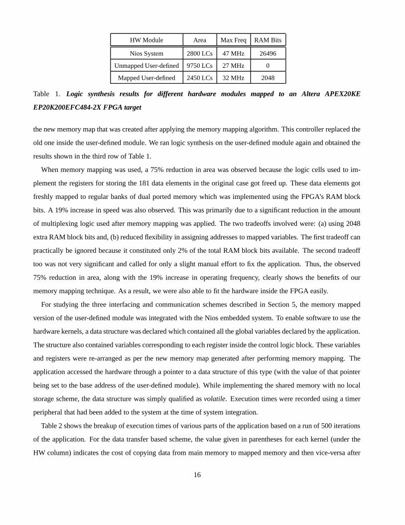
HW Module Area Max Freq RAM Bits
Nios System 2800 LCs 47 MHz 26496
Unmapped User-defined 9750 LCs 27 MHz 0
Mapped User-defined 2450 LCs 32 MHz 2048
Table 1. Logic synthesis results for different hardware modules mapped to an Altera APEX20KE
EP20K200EFC484-2X FPGA target
the new memory map that was created after applying the memory mapping algorithm. This controller replaced the
old one inside the user-defined module. We ran logic synthesis on the user-defined module again and obtained the
results shown in the third row of Table 1.
When memory mapping was used, a 75% reduction in area was observed because the logic cells used to im-
plement the registers for storing the 181 data elements in the original case got freed up. These data elements got
freshly mapped to regular banks of dual ported memory which was implemented using the FPGA’s RAM block
bits. A 19% increase in speed was also observed. This was primarily due to a significant reduction in the amount
of multiplexing logic used after memory mapping was applied. The two tradeoffs involved were: (a) using 2048
extra RAM block bits and, (b) reduced flexibility in assigning addresses to mapped variables. The first tradeoff can
practically be ignored because it constituted only 2% of the total RAM block bits available. The second tradeoff
too was not very significant and called for only a slight manual effort to fix the application. Thus, the observed
75% reduction in area, along with the 19% increase in operating frequency, clearly shows the benefits of our
memory mapping technique. As a result, we were also able to fit the hardware inside the FPGA easily.
For studying the three interfacing and communication schemes described in Section 5, the memory mapped
version of the user-defined module was integrated with the Nios embedded system. To enable software to use the
hardware kernels, a data structure was declared which contained all the global variables declared by the application.
The structure also contained variables corresponding to each register inside the control logic block. These variables
and registers were re-arranged as per the new memory map generated after performing memory mapping. The
application accessed the hardware through a pointer to a data structure of this type (with the value of that pointer
being set to the base address of the user-defined module). While implementing the shared memory with no local
storage scheme, the data structure was simply qualified as volatile. Execution times were recorded using a timer
peripheral that had been added to the system at the time of system integration.
Table 2 shows the breakup of execution times of various parts of the application based on a run of 500 iterations
of the application. For the data transfer based scheme, the value given in parentheses for each kernel (under the
HW column) indicates the cost of copying data from main memory to mapped memory and then vice-versa after
16
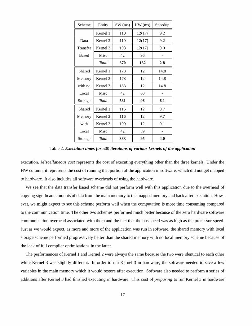
Scheme Entity SW (ms) HW (ms) Speedup
Kernel 1 110 12 � 17 � 9 � 2
Data Kernel 2 110 12 � 17 � 9 � 2
Transfer Kernel 3 108 12 � 17 � 9 � 0
Based Misc 42 96 -
Total 370 132 2 � 8
Shared Kernel 1 178 12 14 � 8
Memory Kernel 2 178 12 14 � 8
with no Kernel 3 183 12 14 � 8
Local Misc 42 60 -
Storage Total 581 96 6 � 1
Shared Kernel 1 116 12 9 � 7
Memory Kernel 2 116 12 9 � 7
with Kernel 3 109 12 9 � 1
Local Misc 42 59 -
Storage Total 383 95 4 � 0
Table 2. Execution times for 500 iterations of various kernels of the application
execution. Miscellaneous cost represents the cost of executing everything other than the three kernels. Under the
HW column, it represents the cost of running that portion of the application in software, which did not get mapped
to hardware. It also includes all software overheads of using the hardware.
We see that the data transfer based scheme did not perform well with this application due to the overhead of
copying significant amounts of data from the main memory to the mapped memory and back after execution. How-
ever, we might expect to see this scheme perform well when the computation is more time consuming compared
to the communication time. The other two schemes performed much better because of the zero hardware software
communication overhead associated with them and the fact that the bus speed was as high as the processor speed.
Just as we would expect, as more and more of the application was run in software, the shared memory with local
storage scheme performed progressively better than the shared memory with no local memory scheme because of
the lack of full compiler optimizations in the latter.
The performances of Kernel 1 and Kernel 2 were always the same because the two were identical to each other
while Kernel 3 was slightly different. In order to run Kernel 3 in hardware, the software needed to save a few
variables in the main memory which it would restore after execution. Software also needed to perform a series of
additions after Kernel 3 had finished executing in hardware. This cost of preparing to run Kernel 3 in hardware
17
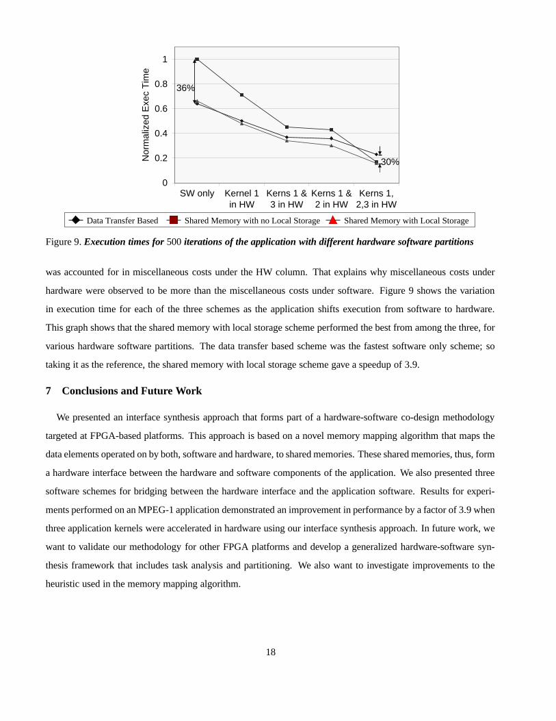
0
0.2
0.4
0.6
0.8
1
SW only Kernel 1in HW
Kerns 1 &3 in HW
Kerns 1 &2 in HW
Kerns 1,2,3 in HW
Nor
mal
ized
Exe
c T
ime
36%
30%
Shared Memory with no Local StorageData Transfer Based Shared Memory with Local Storage
Figure 9. Execution times for 500 iterations of the application with different hardware software partitions
was accounted for in miscellaneous costs under the HW column. That explains why miscellaneous costs under
hardware were observed to be more than the miscellaneous costs under software. Figure 9 shows the variation
in execution time for each of the three schemes as the application shifts execution from software to hardware.
This graph shows that the shared memory with local storage scheme performed the best from among the three, for
various hardware software partitions. The data transfer based scheme was the fastest software only scheme; so
taking it as the reference, the shared memory with local storage scheme gave a speedup of 3 � 9.
7 Conclusions and Future Work
We presented an interface synthesis approach that forms part of a hardware-software co-design methodology
targeted at FPGA-based platforms. This approach is based on a novel memory mapping algorithm that maps the
data elements operated on by both, software and hardware, to shared memories. These shared memories, thus, form
a hardware interface between the hardware and software components of the application. We also presented three
software schemes for bridging between the hardware interface and the application software. Results for experi-
ments performed on an MPEG-1 application demonstrated an improvement in performance by a factor of 3 � 9 when
three application kernels were accelerated in hardware using our interface synthesis approach. In future work, we
want to validate our methodology for other FPGA platforms and develop a generalized hardware-software syn-
thesis framework that includes task analysis and partitioning. We also want to investigate improvements to the
heuristic used in the memory mapping algorithm.
18
Acknowledgments
This project is funded by the Semiconductor Research Corporation under Task I.D. 781.001.
References
[1] A. Sangiovanni-Vincentelli and G. Martin. Platform-based design and software design methodology for
embedded systems. IEEE Design and Test of Computers, December 2001.
[2] R.K. Gupta and G. De Micheli. Hardware-software cosynthesis for digital systems. IEEE Design and Test
of Computers, September 1993.
[3] R. Camposano and R. Brayton. Partitioning before logic synthesis. In International Conference on Computer
Aided Design, 1987.
[4] S. Gupta, N.D. Dutt, R.K. Gupta, and A. Nicolau. Spark : A high-level synthesis framework for applying
parallelizing compiler transformations. In International Conference on VLSI Design, 2003.
[5] R. Camposano and W. H. Wolf. High-Level VLSI Synthesis. Kluwer Academic, 1991.
[6] P.Chou, R.Ortega, and G.Borriello. Interface co-synthesis techniques for embedded systems. In International
Conference on Computer Aided Design, 1995.
[7] J. Daveau, G.F. Marchioro, T. Ben-Ismail, and A.A. Jerraya. Protocol selection and interface generation for
hw-sw codesign. IEEE Transactions on VLSI Systems, March 1997.
[8] Z. Chen et al.˙Pilot - a platform-based hw/sw synthesis system for FPSoC. In Workshop on Software Support
for Reconfigurable Systems, 2003.
[9] M.Balakrishnan, A.K.Majumdar, D.K.Banerji, J.G.Linders, and J.C.Majithia. Allocation of multiport memo-
ries in data path synthesis. IEEE Transactions on Computer Aided Design of Integrated Circuits and Systems,
April 1988.
[10] L. Stok. Data path synthesis. Integration, The VLSI Journal, 1994.
[11] G. De Micheli. Synthesis and Optimization of Digital Circuits. McGraw Hill, 1994.
[12] I. Ouaiss and R. Vemuri. Hierarchical memory mapping during synthesis in FPGA-based reconfigurable
computers. In Design Automation and Test in Europe, 2001.
19
[13] F. Balasa, F. Catthoor, and H.De Man. Dataflow-driven memory allocation for multi-dimensional signal
processing systems. In International Conference on Computer Aided Design, 1994.
[14] W.K.C. Ho and S.J.E. Wilton. Logical-to-physical memory mapping for FPGAs with dual-port embedded
arrays. In International Workshop on FPL and Applications, 1999.
[15] D. Karchmer and J. Rose. Definition and solution of the memory packing problem for field-programmable
systems. In International Conference on Computer Aided Design, 1994.
[16] D.D. Gajski, J. Zhu, R. Domer, A. Gerstlauer, and S. Zhao. SpecC: Specification Language and Methodology.
Kluwer Academic, 2000.
[17] Synopsys Inc. SystemC Reference Manual. http://www.systemc.org.
[18] S. Vernalde, P. Schaumont, and I. Bolsens. An object oriented approach for hardware design. In IEEE
Computer Society Workshop on VLSI, April 1999.
[19] The Altera Website. http://www.altera.com.
[20] The Xilinx Website. http://www.xilinx.com.
[21] E.G. Woutersen and S.H. Gerez. Some complexity results in memory mapping. In Third HCM BELSIGN
Workshop, 1996.
20