Embed Size (px)
Citation preview

Integration, Implementation and Testing of the X-Band SASAR II
System
Georgie George
A dissertation submitted to the Department of Electrical Engineering, University of Cape Town, in
fulfilment of the requirements for the degree of Master of Science in Engineering
Cape Town, 1 December 2007

Department ofElectrical Engineering
For my family...
i

Declaration
I declare that this dissertation is my own, unaided work. It is being submitted for the degree of Master of Science in
Engineering in the University of Cape Town. It has not been submitted before for any degree or examination in any
other university.
Signature of Author . . . . . . . . . . . . . . . . . . . . . . . . . . . . . . . . . .. . . . . . . . . . . . . . . . . . . . . . . . . . . . . . . . . . . . . . . . . . . . . . . . . . .. . . .
Cape Town
1 December 2007
ii

Abstract
This dissertation focuses on the integration, implementation and testing of the X-Band (9.3 GHz) South African Syn-
thetic Aperture Radar project (SASAR II). The SASAR II system was divided into three main subsystems for design
and implementation at M.Sc. level. The three main systems were the transmitter and frequency distribution unit (FDU),
the receiver and the radar digital unit (RDU). Although all subsystems are separate units, the design process was a
collaborative effort.
The purpose of a synthetic aperture radar (SAR) is to providehigh resolution images of extensive areas from airborne
platforms operating from long ranges. The SASAR II project was born out of the success of its predecessor, SASAR,
which was a VHF SAR commissioned in 2000. The SASAR II system is a wide bandwidth X-Band radar system with a
high resolution of 2x2m. The processed resolution of the SASAR II system is enhanced through design improvements
of the transmitted bandwidth, pulse coding and the overall system coherency.
The purpose of this dissertation is to verify the original design specifications of the system and to test its integrity when
all subsystems are combined. The critical parameters for monitoring and testing are the power budget levels for each
RF unit. An insufficient input drive for a mixer may result in anull output. Conversely a high input drive will result in
the saturation of the device and the generation of intermodulation products and higher conversion losses.
Testing of the digital pulse generator (DPG), which is part of the RDU, showed a drop in the specified output power of
10 dB. The power budget calculations made for the transmitter were made based on the input power of the DPG. The
DPG unit also failed to provide adequate port to port isolation between the input trigger and the I & Q output channels.
Spurious harmonics signals from the trigger resulted in aliasing with the IF frequencies. An extra filtering stage was
added at the front end to isolate these harmonics.
The sensitivity time control (STC) and the manual gain control (MGC) form the final amplification/attenuation stages
of the receiver unit. The combination of the two units results in final output signal amplitudes of between 2.15 dBm and
32.5 dBm. The specified maximum input power of the ADC is 10 dBm. The additional gain stages in the MGC would
drive the ADC into saturation and possibly result in permanent damage. The testing of the receiver and the ADC was
therefore limited to low power testing.
The complete system response closely matched that of the design specification. The sources of the spurious signals
described in the previous dissertations were isolated and filtered out. This however required the use of pulsed RF
measurement techniques, specifically regarding the use of the pulse desensitization factor (PDF). Since the tested signals
have a PRF, the measurement equipment takes an average of thepeak pulse power distributed over all the spectral
components over a given PRI. The PDF therefore compensates for the drop in signal power.
iii

Acknowledgements
The number of people that have contributed to this moment, both directly and indirectly, are numerous, and I ask for
understanding should you not be included in my acknowledgements.
I would firstly like to thank my supervisor, Professor Michael Inggs, for his guidance, support, understanding and faith
throughout the duration of this project. The professionalism and the technical abilities imparted to me by him over the
years helped me to develop as a person and as an engineer, and for this I will always be grateful.
I would like to thank the Radar Remote Sensing Group, and especially Dr. Richard, Reggie Lord and Thomas Bennett,
who offered continuous guidance and support during this project. Your understanding, guidance, support and friendship
truly made the last few years some of the most memorable of my life.
I would like to thank my loyal friends who pushed and supported me over the last few years to finish off this project,
especially, Rubia, Lance, Murray, Tim, Wayne, Monica, Greg, Kath, Wesley, Jason, Melanie, Itai, James and Gondai.
I would also like to thank my dog Whip, for not eating any of my drafts and for his understanding when I forgot to walk
him during this period.
And finally, many thanks to my mother, father and sister for their continued support and love. There are no words to
adequately express my undying gratitude to you all, and I only hope that the way I conduct myself in life will be a
testament to your love and faith in me.
iv

Contents
Declaration ii
Abstract iii
Acknowledgements iv
Nomenclature xv
1 Introduction 1
1.1 Terms of Reference . . . . . . . . . . . . . . . . . . . . . . . . . . . . . . . .. . . . . . . . . . . . . 1
1.2 Background to SASAR II . . . . . . . . . . . . . . . . . . . . . . . . . . . . .. . . . . . . . . . . . . 2
1.3 Plan of Development . . . . . . . . . . . . . . . . . . . . . . . . . . . . . . .. . . . . . . . . . . . . 2
1.4 System Overview . . . . . . . . . . . . . . . . . . . . . . . . . . . . . . . . . .. . . . . . . . . . . . 4
2 SASAR II Concept 8
2.1 Introduction . . . . . . . . . . . . . . . . . . . . . . . . . . . . . . . . . . . .. . . . . . . . . . . . . 8
2.2 System Modes and States . . . . . . . . . . . . . . . . . . . . . . . . . . . .. . . . . . . . . . . . . . 8
2.2.1 Power Off . . . . . . . . . . . . . . . . . . . . . . . . . . . . . . . . . . . . . .. . . . . . . . 9
2.2.2 Start Up . . . . . . . . . . . . . . . . . . . . . . . . . . . . . . . . . . . . . . .. . . . . . . 9
2.2.3 Initialisation . . . . . . . . . . . . . . . . . . . . . . . . . . . . . . . .. . . . . . . . . . . . 9
2.2.4 Idle/Standby . . . . . . . . . . . . . . . . . . . . . . . . . . . . . . . . . .. . . . . . . . . . 10
2.2.5 Loop Back Testing . . . . . . . . . . . . . . . . . . . . . . . . . . . . . . .. . . . . . . . . . 10
2.2.6 Full Operation . . . . . . . . . . . . . . . . . . . . . . . . . . . . . . . . .. . . . . . . . . . 10
2.3 Transmitter [4] . . . . . . . . . . . . . . . . . . . . . . . . . . . . . . . . . .. . . . . . . . . . . . . 10
v

Department ofElectrical Engineering
2.4 Receiver [12] . . . . . . . . . . . . . . . . . . . . . . . . . . . . . . . . . . . .. . . . . . . . . . . . 11
2.5 RDU and Post Processing[15] . . . . . . . . . . . . . . . . . . . . . . . .. . . . . . . . . . . . . . . 11
3 Subsystem Analysis 19
3.1 Transmitter . . . . . . . . . . . . . . . . . . . . . . . . . . . . . . . . . . . . .. . . . . . . . . . . . 19
3.1.1 IF1 . . . . . . . . . . . . . . . . . . . . . . . . . . . . . . . . . . . . . . . . . . .. . . . . . 20
3.1.2 IF2 . . . . . . . . . . . . . . . . . . . . . . . . . . . . . . . . . . . . . . . . . . .. . . . . . 21
3.1.3 RF and BIT . . . . . . . . . . . . . . . . . . . . . . . . . . . . . . . . . . . . . .. . . . . . . 22
3.1.4 Transmitter Design Specifications . . . . . . . . . . . . . . . .. . . . . . . . . . . . . . . . . 23
3.2 Frequency Distribution Unit . . . . . . . . . . . . . . . . . . . . . . .. . . . . . . . . . . . . . . . . 23
3.3 Receiver Unit . . . . . . . . . . . . . . . . . . . . . . . . . . . . . . . . . . . .. . . . . . . . . . . . 26
3.3.1 RF . . . . . . . . . . . . . . . . . . . . . . . . . . . . . . . . . . . . . . . . . . . .. . . . . . 26
3.3.2 2nd IF . . . . . . . . . . . . . . . . . . . . . . . . . . . . . . . . . . . . . . . . . . . . . . . . 27
3.3.3 1st IF, Sensitivity Time Control (STC) . . . . . . . . . . . . . . . . . . . . .. . . . . . . . . . 28
3.3.4 1st IF, Manual Gain Control (MGC) . . . . . . . . . . . . . . . . . . . . . . . . . .. . . . . . 29
3.3.5 Receiver Design Specifications . . . . . . . . . . . . . . . . . . .. . . . . . . . . . . . . . . . 30
3.4 Radar Digital Unit (RDU) . . . . . . . . . . . . . . . . . . . . . . . . . . .. . . . . . . . . . . . . . 30
3.4.1 Sampling Techniques . . . . . . . . . . . . . . . . . . . . . . . . . . . .. . . . . . . . . . . . 31
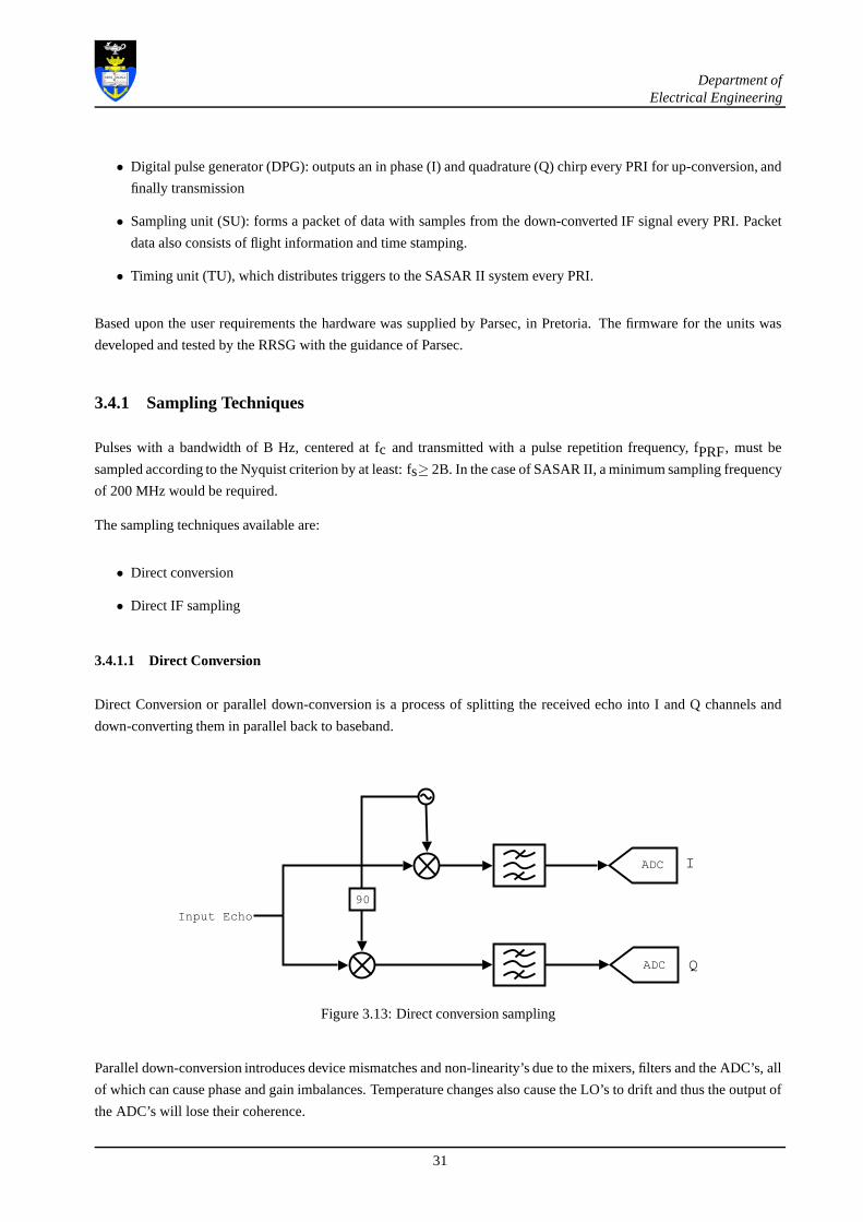
3.4.1.1 Direct Conversion . . . . . . . . . . . . . . . . . . . . . . . . . . . .. . . . . . . . 31
3.4.1.2 Direct IF Sampling . . . . . . . . . . . . . . . . . . . . . . . . . . . .. . . . . . . 32
3.4.2 RDU Hardware Modules . . . . . . . . . . . . . . . . . . . . . . . . . . . .. . . . . . . . . . 32
3.4.2.1 DPG (PM488) . . . . . . . . . . . . . . . . . . . . . . . . . . . . . . . . . .. . . . 32
3.4.2.2 SU (PM480) . . . . . . . . . . . . . . . . . . . . . . . . . . . . . . . . . . .. . . . 33
3.4.2.3 TU (PM440) . . . . . . . . . . . . . . . . . . . . . . . . . . . . . . . . . . .. . . 35
3.4.3 The Design Specifications of the RDU: . . . . . . . . . . . . . . .. . . . . . . . . . . . . . . 35
4 System Integration 36
4.1 SASAR II Housing Unit . . . . . . . . . . . . . . . . . . . . . . . . . . . . . .. . . . . . . . . . . . 36
4.2 RCU System Requirements . . . . . . . . . . . . . . . . . . . . . . . . . . .. . . . . . . . . . . . . . 36
vi

Department ofElectrical Engineering
4.2.1 RCU Overview . . . . . . . . . . . . . . . . . . . . . . . . . . . . . . . . . . .. . . . . . . . 38
4.2.2 FDU Control . . . . . . . . . . . . . . . . . . . . . . . . . . . . . . . . . . . .. . . . . . . . 39
4.2.3 Switch Operations . . . . . . . . . . . . . . . . . . . . . . . . . . . . . .. . . . . . . . . . . 39
4.2.4 Sensitivity Time Control (STC) . . . . . . . . . . . . . . . . . . .. . . . . . . . . . . . . . . 40
4.2.5 Manual Gain Control (MGC) . . . . . . . . . . . . . . . . . . . . . . . .. . . . . . . . . . . . 41
4.2.6 RCU Implementation . . . . . . . . . . . . . . . . . . . . . . . . . . . . .. . . . . . . . . . . 41
4.2.6.1 Description . . . . . . . . . . . . . . . . . . . . . . . . . . . . . . . . .. . . . . . 41
4.2.6.2 Implementing the Radar Controller Unit on the SBC . .. . . . . . . . . . . . . . . . 41
4.2.6.3 Software . . . . . . . . . . . . . . . . . . . . . . . . . . . . . . . . . . . .. . . . . 42
4.2.6.4 C++ Controller Program . . . . . . . . . . . . . . . . . . . . . . . .. . . . . . . . . 43
4.2.6.5 Linux Device Drivers . . . . . . . . . . . . . . . . . . . . . . . . . .. . . . . . . . 43
4.2.7 Limitations . . . . . . . . . . . . . . . . . . . . . . . . . . . . . . . . . . .. . . . . . . . . . 43
4.2.7.1 Installing a RTOS . . . . . . . . . . . . . . . . . . . . . . . . . . . . .. . . . . . . 43
4.2.7.2 Using a Real Time Clock . . . . . . . . . . . . . . . . . . . . . . . . .. . . . . . . 43
4.3 The RDU . . . . . . . . . . . . . . . . . . . . . . . . . . . . . . . . . . . . . . . . . .. . . . . . . . 43
4.3.1 PMA-P: Peritek Passive PMC to PCI Card . . . . . . . . . . . . . .. . . . . . . . . . . . . . 44
4.3.2 PMB-P: Peritek Active PMC to PCI Card . . . . . . . . . . . . . . .. . . . . . . . . . . . . . 44
4.4 Power Supply Unit . . . . . . . . . . . . . . . . . . . . . . . . . . . . . . . . .. . . . . . . . . . . . 45
4.4.1 PSU User Requirements . . . . . . . . . . . . . . . . . . . . . . . . . . .. . . . . . . . . . . 45
4.4.2 SASAR II PSU . . . . . . . . . . . . . . . . . . . . . . . . . . . . . . . . . . . .. . . . . . . 46
4.5 Conclusions . . . . . . . . . . . . . . . . . . . . . . . . . . . . . . . . . . . . .. . . . . . . . . . . . 47
5 Subsystem Testing 48
5.1 FDU Testing . . . . . . . . . . . . . . . . . . . . . . . . . . . . . . . . . . . . . .. . . . . . . . . . . 48
5.1.1 Testing Methodology . . . . . . . . . . . . . . . . . . . . . . . . . . . .. . . . . . . . . . . . 49
5.1.2 Results and Analysis . . . . . . . . . . . . . . . . . . . . . . . . . . . .. . . . . . . . . . . . 50
5.1.3 Conclusion . . . . . . . . . . . . . . . . . . . . . . . . . . . . . . . . . . . .. . . . . . . . . 50
5.2 DPG Testing . . . . . . . . . . . . . . . . . . . . . . . . . . . . . . . . . . . . . .. . . . . . . . . . . 51
5.2.1 Band-Limit . . . . . . . . . . . . . . . . . . . . . . . . . . . . . . . . . . . .. . . . . . . . . 51
vii

Department ofElectrical Engineering
5.2.2 No Band-Limit . . . . . . . . . . . . . . . . . . . . . . . . . . . . . . . . . .. . . . . . . . . 52
5.2.3 Conclusion . . . . . . . . . . . . . . . . . . . . . . . . . . . . . . . . . . . .. . . . . . . . . 53
5.3 ADC Testing . . . . . . . . . . . . . . . . . . . . . . . . . . . . . . . . . . . . . .. . . . . . . . . . 53
5.3.1 The Active Card . . . . . . . . . . . . . . . . . . . . . . . . . . . . . . . . .. . . . . . . . . 55
5.3.2 The Passive Card . . . . . . . . . . . . . . . . . . . . . . . . . . . . . . . .. . . . . . . . . . 55
5.3.3 Testing Methodology . . . . . . . . . . . . . . . . . . . . . . . . . . . .. . . . . . . . . . . . 56
5.3.4 Test Results . . . . . . . . . . . . . . . . . . . . . . . . . . . . . . . . . . .. . . . . . . . . . 56
5.3.4.1 DPG on passive card, ADC on active card (clocked externally 105 MHz) . . . . . . . 56
5.3.4.2 DPG on active card, ADC on passive card (clocked externally 105 MHz) . . . . . . . 57
5.3.4.3 DPG on passive card, ADC on active card (clocked externally 105 MHz: clock
jumpers were changed) . . . . . . . . . . . . . . . . . . . . . . . . . . . . . . . .. 58
5.3.5 Conclusion . . . . . . . . . . . . . . . . . . . . . . . . . . . . . . . . . . . .. . . . . . . . . 58
5.4 Transmitter Testing . . . . . . . . . . . . . . . . . . . . . . . . . . . . . .. . . . . . . . . . . . . . . 60
5.4.1 Equipment Used and Testing Methodology . . . . . . . . . . . .. . . . . . . . . . . . . . . . 60
5.4.2 Testing Results . . . . . . . . . . . . . . . . . . . . . . . . . . . . . . . .. . . . . . . . . . . 61
5.4.3 Conclusions . . . . . . . . . . . . . . . . . . . . . . . . . . . . . . . . . . .. . . . . . . . . . 68
5.5 Receiver Testing . . . . . . . . . . . . . . . . . . . . . . . . . . . . . . . . .. . . . . . . . . . . . . 68
5.5.1 Equipment Used and Methodology . . . . . . . . . . . . . . . . . . .. . . . . . . . . . . . . 68
5.5.2 RF Testing Results . . . . . . . . . . . . . . . . . . . . . . . . . . . . . .. . . . . . . . . . . 69
5.5.3 ADC Sampling Results . . . . . . . . . . . . . . . . . . . . . . . . . . . .. . . . . . . . . . . 75
5.5.3.1 1st Test . . . . . . . . . . . . . . . . . . . . . . . . . . . . . . . . . . . . . . . . . . 75
5.5.3.2 No Band Limiting . . . . . . . . . . . . . . . . . . . . . . . . . . . . . .. . . . . . 80
5.5.3.3 Band Limited . . . . . . . . . . . . . . . . . . . . . . . . . . . . . . . . .. . . . . 84
5.5.4 Conclusions . . . . . . . . . . . . . . . . . . . . . . . . . . . . . . . . . . .. . . . . . . . . . 87
6 Conclusions 89
6.1 System Integration . . . . . . . . . . . . . . . . . . . . . . . . . . . . . . .. . . . . . . . . . . . . . 89
6.2 Subsystem Testing . . . . . . . . . . . . . . . . . . . . . . . . . . . . . . . .. . . . . . . . . . . . . 89
6.2.1 FDU Testing . . . . . . . . . . . . . . . . . . . . . . . . . . . . . . . . . . . .. . . . . . . . 89
viii

Department ofElectrical Engineering
6.2.2 DPG . . . . . . . . . . . . . . . . . . . . . . . . . . . . . . . . . . . . . . . . . . .. . . . . 90
6.2.3 Transmitter . . . . . . . . . . . . . . . . . . . . . . . . . . . . . . . . . . .. . . . . . . . . . 90
6.2.4 Receiver . . . . . . . . . . . . . . . . . . . . . . . . . . . . . . . . . . . . . .. . . . . . . . 90
6.2.5 ADC . . . . . . . . . . . . . . . . . . . . . . . . . . . . . . . . . . . . . . . . . . .. . . . . 91
7 Recommendations 92
7.1 SASAR II housing . . . . . . . . . . . . . . . . . . . . . . . . . . . . . . . . . .. . . . . . . . . . . 92
7.2 FDU . . . . . . . . . . . . . . . . . . . . . . . . . . . . . . . . . . . . . . . . . . . . .. . . . . . . . 92
7.3 RDU . . . . . . . . . . . . . . . . . . . . . . . . . . . . . . . . . . . . . . . . . . . . .. . . . . . . . 93
7.4 Transmitter . . . . . . . . . . . . . . . . . . . . . . . . . . . . . . . . . . . . .. . . . . . . . . . . . 93
7.5 Receiver . . . . . . . . . . . . . . . . . . . . . . . . . . . . . . . . . . . . . . . .. . . . . . . . . . . 96
ix

List of Figures
1.1 SASAR II complete system . . . . . . . . . . . . . . . . . . . . . . . . . . .. . . . . . . . . . . . . 5
2.1 Simulation of a sampled chirp waveform . . . . . . . . . . . . . . .. . . . . . . . . . . . . . . . . . . 13
2.2 Time domain matched filter . . . . . . . . . . . . . . . . . . . . . . . . . .. . . . . . . . . . . . . . . 14
2.3 Down-converted chirp waveform . . . . . . . . . . . . . . . . . . . . .. . . . . . . . . . . . . . . . . 15
2.4 Matched filter with a Hamming window . . . . . . . . . . . . . . . . . .. . . . . . . . . . . . . . . . 16
2.5 Time domain focused signal . . . . . . . . . . . . . . . . . . . . . . . . .. . . . . . . . . . . . . . . 17
2.6 Focused point target . . . . . . . . . . . . . . . . . . . . . . . . . . . . . .. . . . . . . . . . . . . . . 18
3.1 Transmitter block diagram . . . . . . . . . . . . . . . . . . . . . . . . .. . . . . . . . . . . . . . . . 20
3.2 Transmitter IF1 . . . . . . . . . . . . . . . . . . . . . . . . . . . . . . . . . .. . . . . . . . . . . . . 20
3.3 Transmitter IF2 . . . . . . . . . . . . . . . . . . . . . . . . . . . . . . . . . .. . . . . . . . . . . . . 21
3.4 Transmitter RF and BIT . . . . . . . . . . . . . . . . . . . . . . . . . . . . .. . . . . . . . . . . . . . 22
3.5 Block diagram of frequency synthesis . . . . . . . . . . . . . . . .. . . . . . . . . . . . . . . . . . . 23
3.6 SASAR II FDU [4] . . . . . . . . . . . . . . . . . . . . . . . . . . . . . . . . . . .. . . . . . . . . . 25
3.7 Receiver block diagram . . . . . . . . . . . . . . . . . . . . . . . . . . . .. . . . . . . . . . . . . . 26
3.8 Receiver RF stage . . . . . . . . . . . . . . . . . . . . . . . . . . . . . . . . .. . . . . . . . . . . . . 26
3.9 Receiver 2nd IF . . . . . . . . . . . . . . . . . . . . . . . . . . . . . . . . . . . . . . . . . . . . . . . 27
3.10 Receiver 1st IF, Sensitivity Time Control (STC) . . . . . . . . . . . . . . . . . . . . .. . . . . . . . . 28
3.11 STC curve [4] . . . . . . . . . . . . . . . . . . . . . . . . . . . . . . . . . . . .. . . . . . . . . . . . 29
3.12 Receiver 1st IF, Manual Gain Control (MGC) . . . . . . . . . . . . . . . . . . . . . . . . . .. . . . . 29
3.13 Direct conversion sampling . . . . . . . . . . . . . . . . . . . . . . .. . . . . . . . . . . . . . . . . . 31
x

Department ofElectrical Engineering
3.14 PM488 system block diagram, physical PMC card . . . . . . . .. . . . . . . . . . . . . . . . . . . . . 33
3.15 PM480 system block diagram, physical PMC card . . . . . . . .. . . . . . . . . . . . . . . . . . . . . 34
4.1 RCU system overview . . . . . . . . . . . . . . . . . . . . . . . . . . . . . . .. . . . . . . . . . . . 38
4.2 SPDT switch layout . . . . . . . . . . . . . . . . . . . . . . . . . . . . . . . .. . . . . . . . . . . . . 39
4.3 RCU implementation for FDU control . . . . . . . . . . . . . . . . . .. . . . . . . . . . . . . . . . . 42
4.4 Peritek passive PMC to PCI adapter card . . . . . . . . . . . . . . .. . . . . . . . . . . . . . . . . . . 44
4.5 Peritek active PMC to PCI adapter card . . . . . . . . . . . . . . . .. . . . . . . . . . . . . . . . . . 45
4.6 Transformer regulatory system . . . . . . . . . . . . . . . . . . . . .. . . . . . . . . . . . . . . . . . 46
4.7 LM317/117 variable voltage regulator . . . . . . . . . . . . . . .. . . . . . . . . . . . . . . . . . . . 46
5.1 FDU testing setup . . . . . . . . . . . . . . . . . . . . . . . . . . . . . . . . .. . . . . . . . . . . . . 49
5.2 Time domain band-limiting using window functions . . . . .. . . . . . . . . . . . . . . . . . . . . . . 51
5.3 Frequency domain band-limiting . . . . . . . . . . . . . . . . . . . .. . . . . . . . . . . . . . . . . . 52
5.4 Time domain based signal with no band-limiting . . . . . . . .. . . . . . . . . . . . . . . . . . . . . 52
5.5 Frequency domain signal with no band-limiting . . . . . . . .. . . . . . . . . . . . . . . . . . . . . . 53
5.6 Original test results of (a) Channel A (b) Channel B (c) Frequency Spectrum (d) A and B combined . . 54
5.7 RDU test setup . . . . . . . . . . . . . . . . . . . . . . . . . . . . . . . . . . . .. . . . . . . . . . . 56
5.8 PMC adapter cards swapped (a) Channel A (b) Channel B (c) Frequency Spectrum (d) A and B combined 57
5.9 Bridge M66EN results (a) Channel A (b) Channel B (c) Frequency Spectrum (d) A and B combined . . 58
5.10 PCI M66EN results (a) Channel A (b) Channel B (c) Frequency Spectrum (d) A and B combined . . . . 59
5.11 PMC M66EN results (a) Channel A (b) Channel B (c) Frequency Spectrum (d) A and B combined . . . 59
5.12 Spurious signals in the frequency domain of the 1st IF . . . . . . . . . . . . . . . . . . . . . . . . . . 61
5.13 Spurious signals at 142 MHz and 174 MHz with IF signal at 158 MHz . . . . . . . . . . . . . . . . . . 62
5.14 I and Q low pass filter S21test . . . . . . . . . . . . . . . . . . . . . . . . . . . . . . . . . . . . . . . 63
5.15 1st IF with spurious signals filtered out . . . . . . . . . . . . . . . . . . . .. . . . . . . . . . . . . . . 63
5.16 DPG output . . . . . . . . . . . . . . . . . . . . . . . . . . . . . . . . . . . . . .. . . . . . . . . . . 64
5.17 RF (9300 MHz) output . . . . . . . . . . . . . . . . . . . . . . . . . . . . . .. . . . . . . . . . . . . 64
5.18 Transmitter IF1 component power levels . . . . . . . . . . . . .. . . . . . . . . . . . . . . . . . . . . 65
xi

Department ofElectrical Engineering
5.19 Transmitter IF2 component power levels . . . . . . . . . . . . .. . . . . . . . . . . . . . . . . . . . . 66
5.20 Transmitter RF component power levels . . . . . . . . . . . . . .. . . . . . . . . . . . . . . . . . . . 67
5.21 Receiver input signal . . . . . . . . . . . . . . . . . . . . . . . . . . . .. . . . . . . . . . . . . . . . 69
5.22 Receiver RF component power levels . . . . . . . . . . . . . . . . .. . . . . . . . . . . . . . . . . . . 70
5.23 Receiver 2nd IF component power level . . . . . . . . . . . . . . . . . . . . . . . . . . . . . .. . . . 71
5.24 Receiver STC component power levels . . . . . . . . . . . . . . . .. . . . . . . . . . . . . . . . . . . 72
5.25 Receiver MGC component power levels (MGC min attenuation of -5dB) . . . . . . . . . . . . . . . . . 73
5.26 Receiver MGC component power levels (MGC max attenuation of -35dB) . . . . . . . . . . . . . . . . 74
5.27 Sampled chirp waveform . . . . . . . . . . . . . . . . . . . . . . . . . . .. . . . . . . . . . . . . . . 75
5.28 Down-converted chirp waveform . . . . . . . . . . . . . . . . . . . .. . . . . . . . . . . . . . . . . 76
5.29 Time domain focused signal . . . . . . . . . . . . . . . . . . . . . . . .. . . . . . . . . . . . . . . . 77
5.30 Focused point target . . . . . . . . . . . . . . . . . . . . . . . . . . . . .. . . . . . . . . . . . . . . . 78
5.31 LO signals for 1st IF (13.73o) . . . . . . . . . . . . . . . . . . . . . . . . . . . . . . . . . . . . . . . 79
5.32 LO signals for 1st IF (84.54o) . . . . . . . . . . . . . . . . . . . . . . . . . . . . . . . . . . . . . . . 79
5.33 Sampled chirp waveform . . . . . . . . . . . . . . . . . . . . . . . . . . .. . . . . . . . . . . . . . . 80
5.34 Down-converted chirp waveform . . . . . . . . . . . . . . . . . . . .. . . . . . . . . . . . . . . . . . 81
5.35 Time domain focused signal . . . . . . . . . . . . . . . . . . . . . . . .. . . . . . . . . . . . . . . . 82
5.36 Focused point target . . . . . . . . . . . . . . . . . . . . . . . . . . . . .. . . . . . . . . . . . . . . . 83
5.37 Sampled chirp waveform . . . . . . . . . . . . . . . . . . . . . . . . . . .. . . . . . . . . . . . . . . 84
5.38 Down-converted chirp waveform . . . . . . . . . . . . . . . . . . . .. . . . . . . . . . . . . . . . . . 85
5.39 Time domain focused signal . . . . . . . . . . . . . . . . . . . . . . . .. . . . . . . . . . . . . . . . 86
5.40 Focused point target . . . . . . . . . . . . . . . . . . . . . . . . . . . . .. . . . . . . . . . . . . . . . 87
7.1 RF transmit power with 15 dB gain correction . . . . . . . . . . .. . . . . . . . . . . . . . . . . . . . 93
7.2 RF signal aliased with LO harmonics . . . . . . . . . . . . . . . . . .. . . . . . . . . . . . . . . . . . 94
7.3 IF and LO leakage at SP1 . . . . . . . . . . . . . . . . . . . . . . . . . . . . .. . . . . . . . . . . . . 94
7.4 F1 transfer function [12] . . . . . . . . . . . . . . . . . . . . . . . . . .. . . . . . . . . . . . . . . . 95
7.5 Additional gain stage before F1 . . . . . . . . . . . . . . . . . . . . .. . . . . . . . . . . . . . . . . . 95
7.6 IF1 modification . . . . . . . . . . . . . . . . . . . . . . . . . . . . . . . . . .. . . . . . . . . . . . 95
xii

Department ofElectrical Engineering
7.7 Adding additional filter after gain stage . . . . . . . . . . . . .. . . . . . . . . . . . . . . . . . . . . 96
8 SASAR II PSU front panel and voltage colour codes . . . . . . . . .. . . . . . . . . . . . . . . . . . 98
9 National Semiconductor pin-outs and cable connectors . . .. . . . . . . . . . . . . . . . . . . . . . . 100
10 Completed synthesizer module . . . . . . . . . . . . . . . . . . . . . . .. . . . . . . . . . . . . . . . 101
11 Synthesizer pin-outs . . . . . . . . . . . . . . . . . . . . . . . . . . . . . .. . . . . . . . . . . . . . . 101
12 Codeloader2 IF and RF tabs . . . . . . . . . . . . . . . . . . . . . . . . . . .. . . . . . . . . . . . . 102
13 Codeloader2 IF and RF tabs . . . . . . . . . . . . . . . . . . . . . . . . . . .. . . . . . . . . . . . . 103
14 Average power . . . . . . . . . . . . . . . . . . . . . . . . . . . . . . . . . . . . .. . . . . . . . . . 105
15 Pulse power . . . . . . . . . . . . . . . . . . . . . . . . . . . . . . . . . . . . . . .. . . . . . . . . . 106
16 Peak envelope power . . . . . . . . . . . . . . . . . . . . . . . . . . . . . . . .. . . . . . . . . . . . 107
17 Pulsed RF measurements (a) narrow-band mode (b) broad-band mode . . . . . . . . . . . . . . . . . . 108
18 Tx: IF1 . . . . . . . . . . . . . . . . . . . . . . . . . . . . . . . . . . . . . . . . . . .. . . . . . . . 110
19 Tx: IF2 . . . . . . . . . . . . . . . . . . . . . . . . . . . . . . . . . . . . . . . . . . .. . . . . . . . 111
20 Tx: IF2 . . . . . . . . . . . . . . . . . . . . . . . . . . . . . . . . . . . . . . . . . . .. . . . . . . . 112
21 Rx: IF1 . . . . . . . . . . . . . . . . . . . . . . . . . . . . . . . . . . . . . . . . . . .. . . . . . . . 113
22 Rx: IF2 . . . . . . . . . . . . . . . . . . . . . . . . . . . . . . . . . . . . . . . . . . .. . . . . . . . 114
23 Rx: STC . . . . . . . . . . . . . . . . . . . . . . . . . . . . . . . . . . . . . . . . . . .. . . . . . . . 115
24 Rx: MGC . . . . . . . . . . . . . . . . . . . . . . . . . . . . . . . . . . . . . . . . . . .. . . . . . . 116
25 FDU1 . . . . . . . . . . . . . . . . . . . . . . . . . . . . . . . . . . . . . . . . . . . . .. . . . . . . 117
26 FDU2 . . . . . . . . . . . . . . . . . . . . . . . . . . . . . . . . . . . . . . . . . . . . .. . . . . . . 118
27 Rx: STC . . . . . . . . . . . . . . . . . . . . . . . . . . . . . . . . . . . . . . . . . . .. . . . . . . . 119
28 Rx: STC . . . . . . . . . . . . . . . . . . . . . . . . . . . . . . . . . . . . . . . . . . .. . . . . . . . 120
29 SASAR II Front Panel . . . . . . . . . . . . . . . . . . . . . . . . . . . . . . . .. . . . . . . . . . . 121
xiii

List of Tables
3.1 Transmitter IF1 component part list . . . . . . . . . . . . . . . . .. . . . . . . . . . . . . . . . . . . 21
3.2 Transmitter IF2 component part list . . . . . . . . . . . . . . . . .. . . . . . . . . . . . . . . . . . . 21
3.3 Transmitter RF component part list . . . . . . . . . . . . . . . . . .. . . . . . . . . . . . . . . . . . . 22
3.4 FDU part list . . . . . . . . . . . . . . . . . . . . . . . . . . . . . . . . . . . . .. . . . . . . . . . . 24
3.5 Receiver RF component part list . . . . . . . . . . . . . . . . . . . . .. . . . . . . . . . . . . . . . . 27
3.6 Receiver 2nd IF component part list . . . . . . . . . . . . . . . . . . . . . . . . . . . . . . . .. . . . 28
3.7 Receiver STC component part list . . . . . . . . . . . . . . . . . . . .. . . . . . . . . . . . . . . . . 29
3.8 Receiver MGC component part list . . . . . . . . . . . . . . . . . . . .. . . . . . . . . . . . . . . . . 30
4.1 Valid combinations . . . . . . . . . . . . . . . . . . . . . . . . . . . . . . .. . . . . . . . . . . . . . 40
4.2 STC characteristics . . . . . . . . . . . . . . . . . . . . . . . . . . . . . .. . . . . . . . . . . . . . . 40
4.3 MGC combinations . . . . . . . . . . . . . . . . . . . . . . . . . . . . . . . . .. . . . . . . . . . . . 41
4.4 Data connections from the TBC . . . . . . . . . . . . . . . . . . . . . . .. . . . . . . . . . . . . . . 42
4.5 SASAR II voltage and power requirements . . . . . . . . . . . . . .. . . . . . . . . . . . . . . . . . 45
5.1 FDU LO power levels . . . . . . . . . . . . . . . . . . . . . . . . . . . . . . . .. . . . . . . . . . . . 50
xiv
Nomenclature
ADC – Analog to Digital Converter (Parsec PM480)
C-Band – Frequency Range from 4 - 8 GHz
DAC – Digital to Analog Converter
DPG – Digital Pulse Generator (Parsec PM488)
DSU – Data Storage Unit
FDU – Frequency Distribution Unit
FFT – Fast Fourier Transform
GPS– Global Positioning System
GUI – Graphical User interface
IF – Intermediate Frequency
JTAG – Joint Test Action Group
L-Band – Frequency Range from 2 - 4 GHz
LNA – Low Noise Amplifier
LO – Local Oscillator
MGC – Manual Gain Control
MS/s – Mega Samples per second
NAV – Navigation Unit
PM480– See ADC
PM488– See DPG
PMC – PCI Mezzanine Card
PRF – Pulse Repetition Frequency
xv

Department ofElectrical Engineering
PRI – Pulse Repetition Interval
PSU– Power Supply Unit
RCU – Radar Controller Unit
RDU – Radar Digital Unit
RFU – Radar Frequency Unit
SAR – Synthetic Aperture Radar
SASAR II – South African Synthetic Aperture Radar II
SMA – Subminiature Version A
SNR – Signal to Noise Ratio
SPDT– Single Pole Double Throw
STALO – Stable Local Oscillator
STC – Sensitivity Time Control
TU – Timing Unit (Parsec PM440)
UCT – University of Cape Town
UDP – User Datagram Packets
VHF – Very High Frequency
X-Band – Frequency Range from 8 - 12 GHz
xvi

Chapter 1
Introduction
This dissertation describes the process behind the integration, implementation and testing of the X-Band SASAR II
system. The scope of the project involved the integration ofall completed subsystems by past M.Sc. students. The
completed subsystems concerned are:
• The Transmitter (T x) and Frequency Distribution Unit (FDU) [4]
• The Receiver Unit (Rx ) [12]
• The Radar Digital Unit (RDU) [15]
The SASAR II system has been an ongoing project for the past few years and its aim is to consolidate and develop the
South African Synthetic Aperture Radar (SASAR) capability. The project was a collaboration between a consortium of
companies, namely SunSpace, Kentron and UCT. The enhancement of skills and development of resources within the
Radar Remote Sensing Group (RRSG) is considered a core priority in this venture. The SASAR II project was initiated
after the success of its predecessor, SASAR, which is a VHF synthetic aperture radar (SAR) system. The SASAR II
system was discontinued due to a lack of funding and interestby the consortium. The project has since been revived
and is being continued solely on a student level with supportfrom UCT.
SAR systems take advantage of the long-range propagation characteristics of microwave signals and the complex in-
formation processing capability of modern digital electronics to provide high resolution imagery from airborne moving
platforms such as airplanes and satellites. Synthetic aperture radar complements photographic and other optical imaging
capabilities because of the minimum constraints on time-of-day and atmospheric conditions and because of the unique
responses of terrain and natural targets to radar frequencies [5].
1.1 Terms of Reference
The terms of reference for this dissertation as specified by M.R Inggs [6, 2, 11, 3, 7] and R.T Lord are to:
• Integrate the components and completed subsystems of the SASAR II radar system (RFU, RDU)
1
Department ofElectrical Engineering
• Design, construct and integrate a Power Supply Unit (PSU)
• Design, construct and integrate a Radar Controller Unit (RCU)
• Test and analyze system performance vs. the design specifications
• Document in detail any areas of nonperformance within the system
• Make appropriate recommendations on further development
Due to the unavailability of the X-Band power amplification units, the scope of this dissertation will be limited to low
power loop back testing at the final transmit frequency of 9.3GHz.
It is not within the scope of this dissertation to perform high power testing at X-Band. As a result the testing of the
system will be limited only to low power testing. It is also not within the scope of this dissertation to fully integrate the
antenna into the radar system.
1.2 Background to SASAR II
SASAR II was initiated after the success of its predecessor,SASAR. SASAR is the South African Synthetic Aperture
Radar, operating in the VHF band with a bandwidth of 12 MHz. A SAR operating at lower frequencies has better foliage
and ground penetration as compared with similar radars operating at substantially higher frequencies. The limiting
factor of SASAR was that the frequency band of operation was cluttered with interferences from radio communications.
Interference suppression algorithms were developed by theRRSG and were incorporated into the signal processor. To
achieve a high resolution bandwidth a longer synthetic aperture was required, which implies a longer flight path. This
ultimately had implications on the motion compensation of the system. SASAR was mounted on a C47TP (Turbo Dak),
from the South African Air force. The ultimate success and processing of digital images from the SASAR system gave
rise to the concept of developing an X-Band high bandwidth SAR system. The superheterodyne transceiver design of
the SASAR II system allows for multiple frequency modes of operation with a high processed resolution of 2m.
1.3 Plan of Development
Chapter 2: The system design as explained in section 1.4 gives a high level overview of the complete radar and its
subsystems. This chapter gives a system level description of the functional specifications of SASAR II through its
various modes and states. These modes and states are the highlevel system functionality that is detailed by [4][12][15].
Chapter 3: To obtain a clear understanding of the operation of the entire system and subsystems, the completed
subsystems namely, the radar frequency unit (RFU) and the radar digital unit (RDU) are reviewed and summarised.
Due to the complexity of each subsystem, they formed part of individual dissertations for past M.Sc. students.
The transmitter unit is designed to up-convert the chirp waveform through two intermediate frequency (IF) stages and
a final RF stage. The concept behind the multiple frequency stages is explained here. The operation of each stage is
reviewed and summarised [4].
2

Department ofElectrical Engineering
The local oscillator for the radar system are generated by the frequency distribution unit (FDU) which consists of a
series of programmable frequency synthesisers, filters andamplifiers. Each synthesizer is driven by a stable crystal
oscillator of 10 MHz. A brief explanation of frequency synthesisers is given as of well as the structure of the completed
FDU [4].
The receiver unit is essentially the reverse process of the transmitter unit, in which the received echo is filtered, am-
plified, down-converted, quantised and eventually sampledfor processing on the ground segment. The process of
extracting the signal of interest buried within the spectraof noise and aliased signals requires stringent filtering and
compression techniques. This section explains the conceptstudy behind the design and implementation of the receiver
stage [12].
The final subsystem reviewed is the radar digital unit (RDU),which consists of the digital pulse generator (DPG), the
sampling unit (SU), and the timing unit (TU) [15].
The DPG is a dual channel, 150 MS/s, 14 bit DAC .This unit generates the I and Q channel chirp signals for up-
conversion by the transmitter unit. The waveforms are clocked externally by the FDU. It is also triggered externally
every pulse repetition interval (PRI). The PRI is dependenton the velocity of the aircraft; the greater the speed, the
smaller the PRI [15].
The SU is a dual channel, 105 MS/s, 14 bit ADC. The SU employs its dual channels to sample the IF at 158 MHz
directly. As with the DPG, the SU is clocked and triggered externally every PRI by the TU [15].
The TU is a generic timing card that produces the system triggers. It is synchronous to the system clocks to ensure
system coherence. It produces the triggers for the DPG and the SU [15].
All cards were supplied by Parsec in Pretoria and the design and implementation of the firmware was done with their
guidance and support.
Chapter 4: This chapter deals with the integration of the completed subsystems into a testing rack. In order to suc-
cessfully integrate and test the system, an adequate housing unit was constructed. All components and subsystems
were mounted onto backing plates and interconnected using semi rigid SMA Q-Flex cables. The major requirements to
successfully integrate the unit was the construction of theradar control unit (RCU) and the power supply unit (PSU).
The RF modules concerned are the amplifiers, switches, attenuators and synthesisers, all of which require power for
operation. The SASAR II system requires a total of 12 different voltages, with each backing plate requiring multiple
voltages.
Chapter 5: This chapter deals with the testing and analysis of all integrated subsystems. Testing procedures were
developed to ensure system was operating within the design specification. Prior to integration, tests were conducted on
individual subsystems to ensure that they were operational.
Tests were performed on the FDU to verify the correct frequency and power levels of the LO signals. The programming
of the FDU is done through the provided Windows based software, Code-Loader2. The FDU provides the LO signals
for both the transmitter and the receiver units. In some cases the LO signal level strength was not high enough, thus
some mixers were being "driven" insufficiently. Where necessary the signal strength is amplified.
The input chirp waveform is tracked through the individual modules of the transmitter to verify the expected output
power levels. In some cases the IF signals were much lower than expected. The methodology for solving this problem
is detailed here. Manual loop back tests were performed to verify the receiver’s output power levels.
3
Department ofElectrical Engineering
The DPG was also tested to determine its maximum range of operation i.e. highest PRF capable, channel integrity,
triggering capability. Testing of the SU was performed to ensure its operational status i.e. sampling frequency, channel
integrity, max samples allowed, writing to PCI bus, storingdata in RAM and hard disk.
Chapter 6: Conclusions on the operation of the system are made and recommendations for future work and improve-
ments are proposed.
1.4 System Overview
The SASAR II system is comprised of various subsystems that are interlinked as shown in the diagram 1.1 :
4

Department ofElectrical Engineering
Figure 1.1: SASAR II complete system
5

Department ofElectrical Engineering
A description of the Systems is given below.
1. The Frequency Distribution Unit (FDU):This unit provides all stable local oscillator (STALO) inputs to the mix-
ers, as well as generating the clocking frequencies for the digital to analogue converter (DAC) and the analogue
to digital converter (ADC). The STALO utilises a stable 10 MHz crystal as its reference.
2. The Radio Frequency Unit (RFU): This unit consists of three subsystems, namely the Transmitter, Receiver and
the Antenna. The transmitter takes a base-band chirp signalproduced by the radar digital unit (RDU) and up-
converts it through 2 intermediate frequency stages (IF) tothe final frequency of 9300 MHz. This signal is
amplified and transmitted via a circulator to the antenna. The antenna then collects the back-scatter energy and
routes it to the receiver unit. This energy is amplified (or attenuated) as required, down-converted and is then
sampled by the RDU. The RFU is controlled by the system controller through the RCU depending on its modes
and states.
3. The Radar Digital Unit (RDU):The RDU consists of the digital pulse generator (DPG), sampling unit (SU) and
timing unit (TU). The DPG generates the dual channel (I and Q)base-banded chirp signal which is supplied to
the RFU. The Sampling Unit samples the IF response from the RFU and time stamps the recorded samples with
data from the NAV unit. This time stamped data is then stored in the data storage unit (DSU). The TU triggers
both the DPG and the SU.
4. The Radar Controller Unit (RCU):The SASAR II system has numerous modules and is complex in nature, there-
fore a single controller unit must be implemented to minimise the number of components within the entire system.
All modes and states of the system will be controlled by this unit, with the oversight of the system controller. The
control of the RFU’s testing system is given to this unit. Output frequencies of the FDU are also determined here.
The pulse repetition frequency (PRF) of the system must varydynamically depending on the speed of the Radar
Platform. A token word is sent from the IMU to the RCU detailing the velocity of the plane. The RCU in turn
sends an output to the TU, which adjusts its DPG trigger accordingly. The final purpose of the RCU is to provide
the RDU with time information gathered from the Navigation Unit, for time stamping and storage in the DSU.
5. The Navigation Unit (NAV):This unit supplies the DSU with position and time information and the RCU with
time information with time information and a ring laser gyro.
6. The Data Storage Unit (DSU):This RAID server stores information from the NAV unit and RDU.
7. The Power Supply:This supplies power to all the above mentioned units.
8. The Ground Segment:This is where all the post-processing is done on informationstored in the DSU.
9. The Radar Platform:This airplane is a twin propeller, pressurised Aero Commander 690A to be hired from the
South African Weather Services.
Due to the complexity of the subsystems, some units were completed as past M.Sc. topics, namely:
• The Transmitter (Tx) and the Frequency Distribution Unit [4].
• The Receiver Unit (Rx ) [12].
• The Radar Digital Unit (RDU) [15].
6

Department ofElectrical Engineering
The design and construction of the antenna unit has been completed by Sifiso Gambahaya, but unfortunately the inte-
gration into the completed radar system is not within the scope of this dissertation.
Since the subsystems mentioned above have been completed and are operational, the next few sections will be spent
reviewing the work covered as detailed in [4][12][15].
7

Chapter 2
SASAR II Concept
2.1 Introduction
The SASAR II radar system was designed for the control and operation by a single user via an Ethernet connection
[4][6][7][12][15][21]. The controller unit controls the initialization and operation of the RF modules within the subsys-
tems. Diagnostic, status, and monitoring signals, from theradar unit are also sent to the user through the controller unit.
Through a series of UDP commands the user can interface with the controller unit and initialize or halt any process (this
includes generating the chirp waveforms and sampling the received signals). The full system design is shown in 1.1.
The heart of the Radar system is the FDU [4], which provides the all subsystems with the necessary clock pulses,
LO frequencies and device triggers, which are generated from a stable clock frequency of 10 MHz. This is done to
maintain coherency through all stages of the radar system. The frequencies are generated by programmable frequency
synthesizers using the National Semiconductor CodeLoader2 software.
The frequencies generated are:
• 150 MHz - DAC I and Q channel clock
• 210 MHz - ADC I and Q channel clock
• 158 MHz 1st IF LO
• 1142 MHz 2nd IF LO
• 8 GHz - RF LO
2.2 System Modes and States
The SASAR II system can be considered as a state machine. The operation of the controller unit is based on the
modes and states of the radar system determined by the user requirements. The sequential modes of operation and their
subsequent states are given below.
8

Department ofElectrical Engineering
• Off (Power Down)
• Start-up (Power Up/Warm Up)
– Synthesiser warm up
– Pre-amplifier and Amplifier warm up
• Initialisation
– Load Linux onto System Controller
– Load Linux onto Radar Controller Unit
– Programming the FDU
• Idle/Standby
• Loop Back Testing
– 1stIF loop back
– 2ndIF loop back
– RF loop back
• Full Operation Mode
2.2.1 Power Off
This is the initial state of the radar unit. The RCU is also in power down mode, no operational information is required.
At this stage the user must be able to switch all the relevant units on.
2.2.2 Start Up
In this mode the radar unit, system controller and the RCU arepowered up. The radar unit requires time to warm up.
The pre-amp and power amplifier needs to be idle for a set period of time before being engaged in the full operating
mode.
2.2.3 Initialisation
At this stage all subsystems are powered up, but they are not operational.
During this time the operating system is loaded onto both thesystem controller and the RCU.
The RCU establishes links between the relevant subsystems and verifies their operational integrity. This information is
outputted back the user via the system controller.
The FDU comprises of 4 digitally controlled Local Oscillators (LO) which provide the radar unit with the desired
frequencies. Each LO requires a serial bit stream from the RCU in order to output the correct frequency. The user
inputs command lines from the system controller that interface with the RCU to program the LO.
9

Department ofElectrical Engineering
2.2.4 Idle/Standby
After the Initialisation mode the system is required to be set to a default mode where is is non operational. This is done
in order to prevent high power signals from being transmitted prematurely. The system can be set to loop back at the
1stIF by default until otherwise specified by the user. An alternative arrangement would be to negate the gating pulse
that the pre-amplifier requires. This would render the pre-amplifier non functional and thus preventing the high power
signals from being transmitted.
2.2.5 Loop Back Testing
The operational integrity of the entire system is of crucialimportance. A non function system results in necessary down
time and hence increased expenses. In order to prevent this rigorous testing must be done prior to take off in order to
verify that the system is operational. The test procedures are executed by the user from the system controller. The RCU
receives these commands and outputs the relevant logic signals to the appropriate switches.
The RCU is required to control the RF switches located in boththe transmitter and the receiver. This allows the user to
route specific IF frequencies from the transmitter stages tothe relevant frequency stages of the receiver.
2.2.6 Full Operation
Once the sequential modes have been completed the system cannow be set to the full operation mode. The RCU
however must inform the system user if it is safe to switch to this mode of operation. A control signal from the dummy
loads needs to be implemented to determine whether the system is set to “dummy load” for testing, or the switch (SW4)
is open for transmission. Once this has been verified the usermust take suitable precautions to prevent exposure to the
antenna’s radiation.
2.3 Transmitter [4]
The DAC (Parsec PMC 488) is triggered by the TU (Parsec PMC 440) every PRI to output an I and Q channel chirp
waveform. The I and Q channels are up-converted to 158 MHz (VHF) through a series of mixers, adders, filters and
switches. The two signals are combined in the 1st stage of thetransmitter. At this point the RADAR can operate
similarly to the existing VHF radar, SASAR, which was completed in 2000 (SASAR II has the advantage of having
a much larger bandwidth of 100 MHz). In order to verify that the system is operational prior to take off, the operator
must be able to loop back the VHF (1st IF) signal to the final stage of the receiver chain (see 1.1). The user controls a
series of single pole double throw (SPDT) switches with UDP commands through the controller unit. This is a matter
of setting the TTL on the switches high or low.
A second stage is used to up-convert the VHF signal to a centerfrequency of 1.3 GHz (L-Band), which is a commonly
used frequency for commercial radar systems. The possibility of high power testing at this stage is being considered,
courtesy of a donation of amplifiers and antennas by Reutech Radar Systems (RRS). As in the VHF stage, prior to take
off, the user will be required to loop the L-Band signal to thesecond stage of the receiver to verify the system power
levels are within specification.
10

Department ofElectrical Engineering
The final X-Band stage of the transmitter consists of a pre-amplifier, a high power TWT amplifier and a built in test
system (BIT). The scope of this dissertation is limited to the generation of the X-Band signal at the input to the pre-
amplifier. At this stage the user is able to loop back the signal which is down-converted to the initial VHF frequency.
The power levels at each relevant frequency are measured to verify system integrity.
2.4 Receiver [12]
The system specification dictates that the waveform from thetransmitter be sent to the pillbox antenna through a
circulator (a three port device that isolates the transmitter from the receiver) for transmission. The received signalis
down-converted through the receiver chain to the 1st IF frequency of 158 MHz. The receiver can be considered as the
mirror of the transmitter, as it is down-converted through asimilar two stage process (of mixers, amplifiers and filters)
before it is sampled by the ADC.
The power of received signals varies depending on the radar cross section (RCS) of the target and the characteristics of
the scanned scene. The two stages that are added to the systemthat compensate for this lack of signal strength is the,
Sensitivity Time Controller (STC), and the Manual Gain Controller (MGC). The STC is a time dependent variable gain
stage, where the return echoes from close by targets are attenuated and the returns from targets at far range are boosted.
For the purposes of this dissertation the STC will be set to the maximum attenuation level of 20 dB.
The MGC is a manually controlled 3 bit attenuator. The user isable to select the degree of attenuation that is required,
from a minimum value of 5 dB to the maximum of 30 dB. The user makes the adjustment based on the strength, or
weakness, of the received echoes. The scene characteristics are also an important consideration when selecting the
levels of attenuation i.e. the returns from scanning acrosspopulated areas with large man made structures would be
sufficiently greater than returns from baron landscapes such as deserts and vegetation.
The final signal after the MGC is split into two channels (I andQ) and is sampled with the ADC (Parsec PM480).
The ADC is triggered by the TU to begin sampling the received echoes on every PRI. The FDU provides the clocking
frequencies for the ADC as well (210 MHz). The maximum input clocking frequency for the PM 480 is rated at 105
MHz. Alterations to the PMC card were subsequently made to allow the received signals to be sampled 180 degrees out
of phase at 105 MHz, to simulate the I and Q channel sampling. The signals are then combined digitally to produce a
baseband signal that has effectively been sampled at 210 MHz. The sampled data is then able to be stored on the system
hard drive for post processing [15].
2.5 RDU and Post Processing[15]
Most radar systems have multiple IF frequencies, this helpsin separating the image frequencies and harmonic signals
from the desired signal. The received echoes from the targetare down-converted through a series of filters, mixers and
amplifiers in order to preserve signal integrity for sampling by the ADC. Figure2.1 shows the simulated time domain and
magnitude spectrum signals of a received chirp pulse. The signal is broken down into its real and imaginary components
centered at 158 MHz. In some cases, as with SASAR II, the received signals are not down-converted to baseband. This
is done to avoid phase distortion and non linearity’s that may be introduced by devices at lower frequencies. This is
11

Department ofElectrical Engineering
done to avoid phase distortion and non linearity’s that may be introduced by devices at lower frequencies. This process
is referred to as direct IF sampling and will be covered in 3.4.1.2.
The desired received signal buried in the sampled signal is often indiscernible. To extract the chirp waveform from the
clutter, a template of the known signal is correlated with the received signal to detect the presence of the template in the
unknown signal. Figure 2.2shows and example of the time and frequency domain matched filter used in the processing
of the received pulses. The matched filter is the optimal linear filter for maximizing the signal to noise ratio (SNR) in
the presence of additive noise. The process of pulse compression as described in?? is an example of matched filtering.
The correlation, and subsequent filtering of the received signal and the matched filter, results in the identification of the
desired signal as shown in figure 2.3.
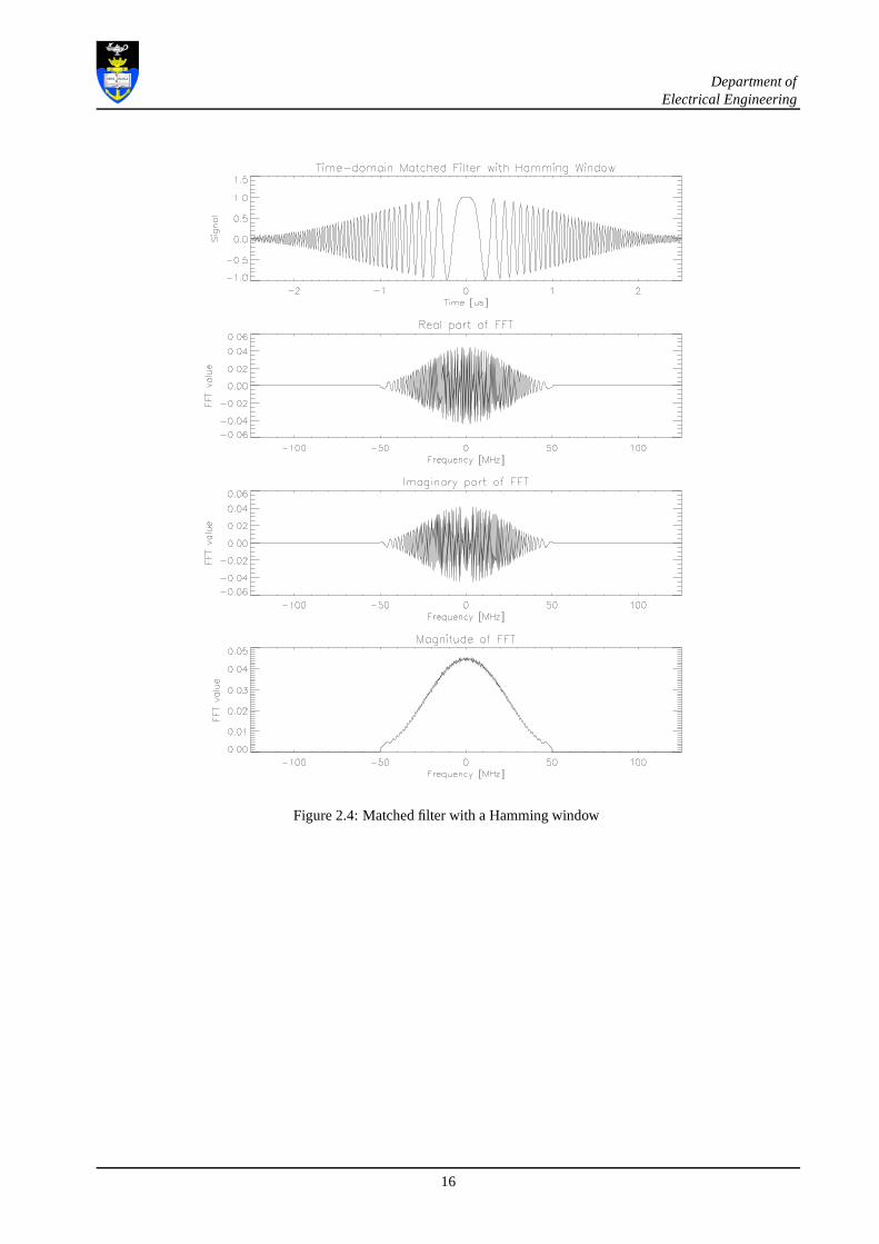
In order to reduce the side-lobes of the focused signal a matching filter with a windowing function can be applied to the
received signal. In signal processing a window function is afunction that is zero valued outside of a chosen interval.
For the purposes of SASAR II processing a matched filter with aHamming window will be used, see figure 2.4 . The
Hamming window is also referred to as a raised cosine window.
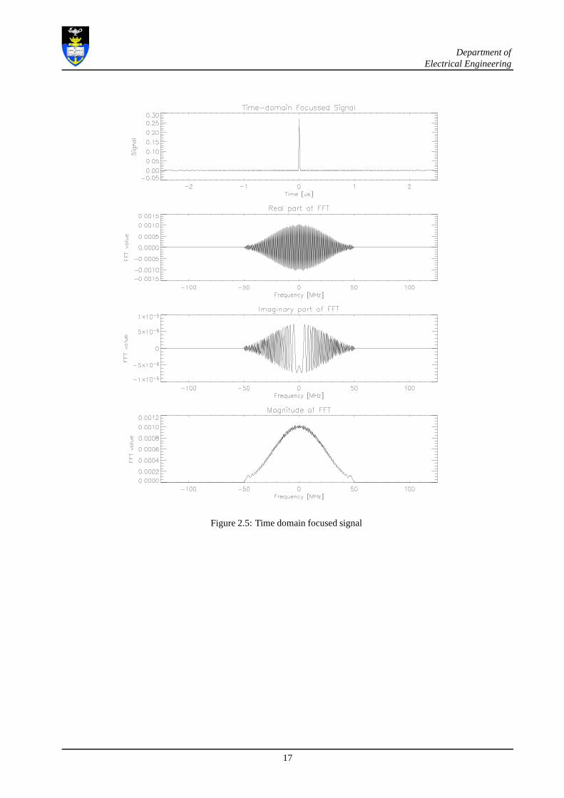
The final focused point target has a pulse width of 0.04 us withthe first side-lobes at -42 dB, see figure 2.6
12

Department ofElectrical Engineering
Figure 2.1: Simulation of a sampled chirp waveform
13

Department ofElectrical Engineering
Figure 2.2: Time domain matched filter
14

Department ofElectrical Engineering
Figure 2.3: Down-converted chirp waveform
15
Department ofElectrical Engineering
Figure 2.4: Matched filter with a Hamming window
16
Department ofElectrical Engineering
Figure 2.5: Time domain focused signal
17

Department ofElectrical Engineering
Figure 2.6: Focused point target
18
Chapter 3
Subsystem Analysis
The completed subsystems that will be covered in this section are:
• The Transmitter (T x) and Frequency Distribution Unit (FDU) [4]
• The Receiver Unit (Rx ) [12]
• The Radar Digital Unit (RDU) [15]
3.1 Transmitter
The transmitter up-converts the low power chirp waveforms through three stages to a final higher power X-Band trans-
mission stage. The FDU produces the local oscillators that drive the mixers. The three stage up-conversion process
serves two ends;
1. Mixing the signals through multiple intermediate IF separates the image frequencies substantially from the desired
signal
2. The multiple frequency stages allow the SASAR II system tooperate at multiple frequency bands i.e. VHF (158
MHz), L-Band (1300 MHz), C-Band (5300 MHz) and X-Band (9300 MHz).
After the considering the operating specifications, the transmitter unit itself was subdivided into four subsystems,
namely:
• IF1
• IF2
• RF
• Built in test system (BIT)
19

Department ofElectrical Engineering
Each subsystem will be reviewed in order to verify its correct operation, as well as its compliance to the design speci-
fications. Gaps that may have occurred during the design and construction process will be filled. The functional block
diagram shown in 3.1 shows the process of up-converting the Iand Q channels through three frequency stages through
to the antenna unit. The design methodologies were verified through examples provided in [27][29].
VHF Radar L Band Radar
1st Upconversion 2nd Upconversion Final Upconversion Power Amplification Built in Test Duplexer
Receiver
Antenna
DPG
I
Q
1st IF (158 MHz) 2nd IF (1300 MHz) RF (9300 MHz)
Figure 3.1: Transmitter block diagram
3.1.1 IF1
Figure 3.2: Transmitter IF1
Two quadrature baseband chirp signals (I and Q) with a real bandwidth of 50 MHz are produced by the DPG . The two
signals are mixed up in frequency to the first IF of 158 MHz (M1 and M2). Both waveforms are combined (SP1) to form
a complex chirp with a bandwidth of 100 MHz. The generation ofthe LO frequencies will be covered in the description
of the FDU. The combined signal is passed through a band pass filter (F1) in order to filter out the spurious image
frequencies and harmonics. The filter (F1) was not deemed crucial in the systems operation, as a result its bandwidth
was set to 140 MHz. The final radar system must have a loop back testing function which allows the system controller
to switch the signals from certain stages in the transmitter(SW1) to the appropriate stages in the receiver (SW6). The
single pole double throw (SPDT) switches (SW1 and SW6) are controlled by a TTL (+5V) logic signal allowing the
20

Department ofElectrical Engineering
user to switch between the IF signals. The control of these switches will be covered in the description of the RCU in
4.2.
Table 3.1: Transmitter IF1 component part listPart ID Part Number Manufacturer Description
MIX 1 ZFM-3 Mini-Circuits MixerMIX 2 ZFM-3 Mini-Circuits MixerSP1 ZFSC-2-1 Mini-Circuits Splitter/Adder
FL1 5BP8-158B120-S Lorch 5thorder Butterworth FilterSW1 ZSDR-230 Mini-Circuits IF Switch
3.1.2 IF2
(Receiver Second Stage: 2Rx)
IF2: 1300MHz
F2
M3
SPDT
1
SW2
SPDT
SW5
1142 MHz
Active L Band Radar
Figure 3.3: Transmitter IF2
As described previously, up-converting the signals through multiple frequency stages relaxes the filtering requirements
by further separating the image frequencies from the desired signals. A second IF of 1300 MHz was chosen for this
stage, making it compatible with commercial L-Band radars.The second criterion for a multiple stage up-conversion
process has now been satisfied. An LO of 1142 MHz is therefore required to mix (M3) up the IF signal at 158 MHz.
The second frequency stage was deemed the most crucial, hence an image rejection mixer (M3) was favoured in place
of a double balanced mixer. The bandwidth of the second filter(F2) was set to 120 MHz. A SPDT switch (SW2) is
utilised to allow the user to switch the L-Band test signal tothe receiver second stage (SW5) for loop back testing.
Table 3.2: Transmitter IF2 component part listPart ID Part Number Manufacturer DescriptionMIX 3 IR0102LC1 Miteq Image rejection mixer
FL2 5BP8-1300/B150-S Lorch 5thorder Butterworth FilterSW2 ZSDR-230 Mini-Circuits IF Switch
21

Department ofElectrical Engineering
3.1.3 RF and BIT
Figure 3.4: Transmitter RF and BIT
The final up-conversion stage of the transmitter mixes (M4) the L-Band frequency component up to the RF frequency
of 9300 MHz. This requires a LO of 8000 MHz. A traveling wave tube amplifier (TWTA) amplifies the RF signal to
3.5 kW. Due to the narrow pass-band of the TWTA, the filters (F3and F4) were omitted. At the time of the design and
testing of the Transmitter unit the TWTA was unavailable, and so conclusive testing regarding its operation could not
be performed.
The testing system consists of the power amplifier (TWTA), the directional coupler (DC1), a transfer switch (SW4), a
dummy load (R1) and two power detectors (D1 & D2). During the pre-flight testing, the correct operation of the TWTA
amplifier needs to be verified. Since the output power of the TWTA amplifier is rated at 3.2 - 4.5 kW, it would not
be safe to perform the test in close proximity. The transfer switch enables the amplified power to be switched into the
dummy load, thereby dissipating all the RF power into heat. The default state of the transmitter will be set to “dummy
load”, once the power levels have been digitised and verified, the system controller can then switch the radar back into
full operation mode. The directional couplers monitor the forward and reverse power flow.
The testing function of the radar unit will be given to the Radar Controller Unit (RCU). All loop back testing and switch
control will be controlled here. The RCU monitors the transmitter power levels during transmission, if the boundary
conditions are exceeded, the TWTA can be shut down.
Table 3.3: Transmitter RF component part listPart ID Part Number Manufacturer Description
MIX 4 M0812-M5 Miteq Double balanced MixerSW3 MSP2t-18 Mini-Circuits IF Switch
AMP 1 N/A Tellumat AmplifierAMP 2 N/A Tellumat Amplifier
22
Department ofElectrical Engineering
3.1.4 Transmitter Design Specifications
The specifications as defined by in [3][2][7], and agreed uponby the system developer [4] are:
• The DAC shall output two channels at maximum power of +10dBm each, with a bandwidth of 50 MHz.
• The system shall have two IF stages at 158 MHz and 1300 MHz, with an RF stage at 9300 MHz.
• System filtering will comprise of 5th order Butterworth filters.
• The transmitted peak power level shall be 3.5 kW.
• The system has a pulse repetition frequency (PRF) of 3 kHz anda pulse length of 5µs.
• The DAC and the ADC shall be clocked with 150 MHz and 210 MHz respectively. The jitter may not exceed
6ρs.
• The system shall have a set of states and modes for testing instructions
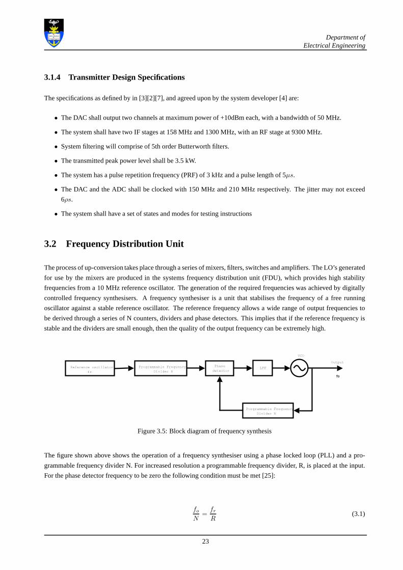
3.2 Frequency Distribution Unit
The process of up-conversion takes place through a series ofmixers, filters, switches and amplifiers. The LO’s generated
for use by the mixers are produced in the systems frequency distribution unit (FDU), which provides high stability
frequencies from a 10 MHz reference oscillator. The generation of the required frequencies was achieved by digitally
controlled frequency synthesisers. A frequency synthesiser is a unit that stabilises the frequency of a free running
oscillator against a stable reference oscillator. The reference frequency allows a wide range of output frequencies to
be derived through a series of N counters, dividers and phasedetectors. This implies that if the reference frequency is
stable and the dividers are small enough, then the quality ofthe output frequency can be extremely high.
Figure 3.5: Block diagram of frequency synthesis
The figure shown above shows the operation of a frequency synthesiser using a phase locked loop (PLL) and a pro-
grammable frequency divider N. For increased resolution a programmable frequency divider, R, is placed at the input.
For the phase detector frequency to be zero the following condition must be met [25]:
fo
N=
fr
R(3.1)
23

Department ofElectrical Engineering
therefore:
fo =N
Rfr (3.2)
Where:
• fo is the output frequency
• fr is the reference frequency
By varying the ratio of N/R a wide range of output frequenciescan be obtained.
The precise operation of the synthesisers will be omitted for the purposes of this dissertation. For further information
on the operation of mixers see [4].
Table 3.4: FDU part listPart ID Part Number Manufacturer Description
Sz1 SPLL-S-A40 Synergy Synthesizer/158 MHzSz2 SPLH-S-A79 Synergy Synthesizer/ 1142 MHzSz3 SPLH-S-4000F Synergy Synthesizer/ 4000 MHzSz4 SPLL-S-A40 Synergy Synthesizer/ 150 MHzSz5 SPLL-S-A40 Synergy Synthesizer/ 210 MHz
SP3 ZBSC615 Mini-Circuits 6-Way splitter
FD F15KXSP Mica Frequency doubler
FL9 3CF6-8000/200-S Lorch 5thorder Butterworth Filter
SP6 ZFSC-2-1 Mini-Circuits Two way splitter
AMP 13-3 N/A Tellumat Amplifier
AMP 13-4 N/A Tellumat Amplifier
SP4 ZMSCQ-2-180 Mini-Circuits 90 degree splitter
SP5 ZFSC-2-1 Mini-Circuits Two way splitter
24

Department ofElectrical Engineering
Figure 3.6: SASAR II FDU [4]
25

Department ofElectrical Engineering
3.3 Receiver Unit
The receiver output is fed into the analogue to digital converter (ADC) for digitization. The appropriate power levels
are thus required to toggle the least significant bit (LSB) ofthe ADC. The receiver is made up of two down conversion
stages consisting of filters, mixers amplifiers and switches. The purpose of the dual stage down conversion process is to
relax the filtering requirements in eliminating the image frequencies.
VHF Radar L Band Radar
Manual Gain Controland Splitter
Sensitivity Time Control
1st Down Conversion
RF InputLNA
Duplexer
Antenna
ADC
I
Q
1st IF (158 MHz) 2nd IF (1300 MHz) RF (9300 MHz)
Figure 3.7: Receiver block diagram
The intermediate frequency of 158 MHz was chosen after considering the maximum sampling rates of 210 MHz of
the ADC (see 3.4.1.2). The second frequency stage of 1300MHz(L-Band) is chosen because of its compatibility with
commercially available L-Band radars. The final RF frequency of 9300MHz (X-Band) was chosen because of the
operating frequency of the TWTA (traveling wave tube amplifier).
3.3.1 RF
SPDT
1
SW4
SW3 (Transmitter)SPDT
LNAAMP 4
FL5
DuplexerTx/Rx Cell
Transmitter
M5
8000 MHz
Antenna
RF: 9300MHzReceiver 1st Stage
Figure 3.8: Receiver RF stage
The first stage of the receiver chain is the RF unit. As described earlier, the receiver unit is essentially the reverse
process of the transmitter stage. The received signal is flitered (FL5) by a 5thorder Butterworth filter centered at 9300
26

Department ofElectrical Engineering
MHz with a bandwidth of 200 MHz. The reason for the relaxed filtering requirements stem from the design strategy
of implementing a dual stage up-conversion/down-conversion process, which results in shifting the image frequency by
2400 MHz to 6700 MHz. The low noise amplifier (LNA - AMP4) has a gain of 22 dB with a noise figure of 0.9 dB.
Although its gain is high, it is low enough to ensure that the receiver is not driven into compression in later stages. SW4
allows the final transmit frequency of the transmitter to be switched into the first RF stage of the receiver. The signal is
then down-converted through the dual stage process and is digitised. The post processing techniques performed on the
digitised data will give an indication whether the system isfunctioning correctly. A double balanced mixer is used at
M5 due to its performance against third order intermodulation distortion.
Table 3.5: Receiver RF component part listPart ID Part Number Manufacture Description
FL5 5WR90-9300/200-S Lorch 5thorder Butterworth FilterSW4 MSP2T-18 Mini-Circuits IF switch
AMP4 AMF-2F-08500960-09-12P Miteq Low noise amplifierMIX 5 M0812-M5 Miteq Double balanced mixer
3.3.2 2nd IF
IF2: 1300MHzReceiver 2nd Stage
FL6M3
1142 MHz
SPDT
SW5
SPDT
AMP 5
SW2 (Transmitter)
Figure 3.9: Receiver 2nd IF
The second IF stage of the receiver takes its input of 1300 MHzfrom the output of the RF stage. This signal is filtered
by a 5thorder Butterworth filter (FL6) centered at 1300 MHz with a bandwidth of 150 MHz. The output of the filter is
amplified (AMP5) by 20 dB. As with the RF stage, the switch (SW5) allows the input to the mixer (M6) to be switched
between the output of AMP 5 and the 2nd IF frequency of the transmitter from SW2. The mixer is also a double
balanced mixer used to convert the L-Band signal to the final IF frequency of 158 MHz.
27

Department ofElectrical Engineering
Table 3.6: Receiver 2nd IF component part listPart ID Part Number Manufacture Description
FL6 58P8-1300/B150-S Lorch 5thorder Butterworth FilterAMP5 ZEL1217LN Mini-Circuits AmplifierSW5 ZSDR-230 Mini-Circuits IF switchMIX6 ZEM-4300-B Mini-Circuits Double balanced mixer
3.3.3 1st IF, Sensitivity Time Control (STC)
IF1: 158 MHzReceiver 1st Stage: STC
FL7
SPDT
SW6
SPDT
AMP 6
SW1 (Transmitter)
Electronic AttenuatorSTC
1
Figure 3.10: Receiver 1st IF, Sensitivity Time Control (STC)
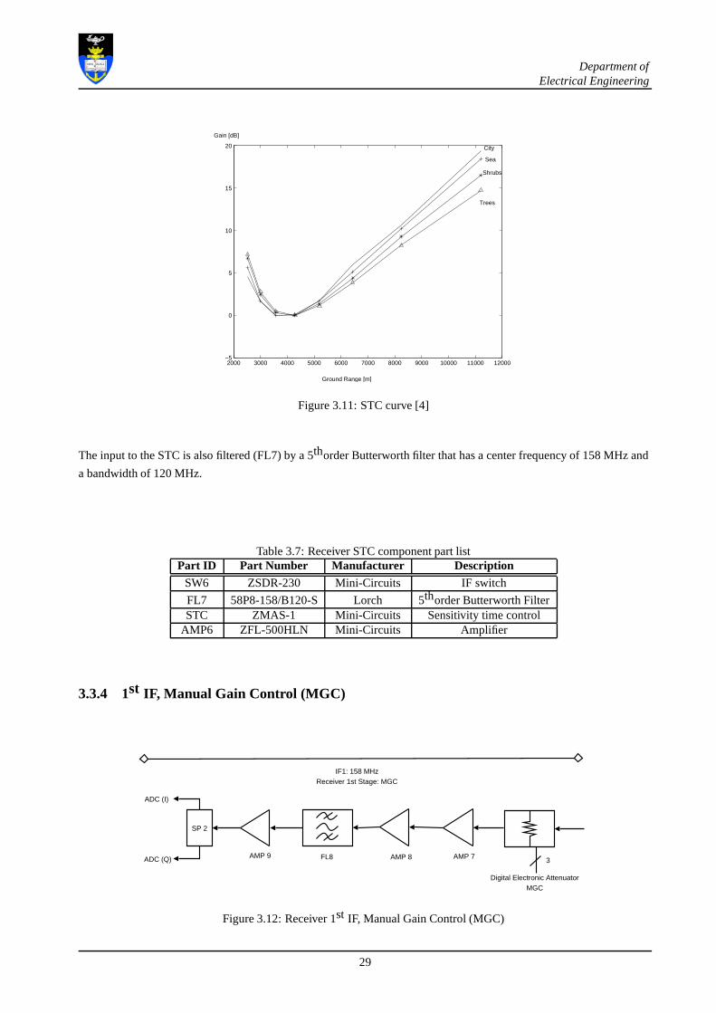
The STC is a time dependent variable gain stage, where the amplitudes of the echoes from targets at far range are
boosted and the amplitudes from strong targets at near rangeare attenuated. The STC has a variable gain of up to 20
dB (cascaded with AMP 6) which is implemented in the radar controller unit (RCU) using an DAC. The values to the
output of the attenuator, as determined by [12] are pre-loaded into the RCU (see image below).
28
Department ofElectrical Engineering
2000 3000 4000 5000 6000 7000 8000 9000 10000 11000 12000−5
0
5
10
15
20
Ground Range [m]
Gain [dB]
City
Sea
Shrubs
Trees
Figure 3.11: STC curve [4]
The input to the STC is also filtered (FL7) by a 5thorder Butterworth filter that has a center frequency of 158 MHz and
a bandwidth of 120 MHz.
Table 3.7: Receiver STC component part listPart ID Part Number Manufacturer Description
SW6 ZSDR-230 Mini-Circuits IF switch
FL7 58P8-158/B120-S Lorch 5thorder Butterworth FilterSTC ZMAS-1 Mini-Circuits Sensitivity time control
AMP6 ZFL-500HLN Mini-Circuits Amplifier
3.3.4 1st IF, Manual Gain Control (MGC)
IF1: 158 MHzReceiver 1st Stage: MGC
FL8AMP 9
Digital Electronic AttenuatorMGC
3AMP 7AMP 8
SP 2
ADC (I)
ADC (Q)
Figure 3.12: Receiver 1st IF, Manual Gain Control (MGC)
29

Department ofElectrical Engineering
The MGC is a 3 bit electronic attenuator followed by three gain blocks (AMP 7, 8, 9). This unit allows the user to
increase the gain of distributed targets at far range, or to attenuate the returns from strong nearby targets. The purpose
of the MGC is to improve the noise figure entering the ADC and toprevent it from being driven into saturation.
Table 3.8: Receiver MGC component part listPart ID Part Number Manufacturer DescriptionMGC ZFAT-51020 Mini-Circuits Manual gain controlAMP7 ZFL-500HLN Mini-Circuits AmplifierAMP8 ZFL-500HLN Mini-Circuits AmplifierAMP9 ZFL-500HLN Mini-Circuits Amplifier
FL8 58P8-158/B100-S Lorch 5thorder Butterworth FilterSP2 ZFSC-2-1 Mini-Circuits Splitter
3.3.5 Receiver Design Specifications
The specifications as defined by in [3][2][7], and agreed uponby the system developer [4] are:
• The received carrier frequency of 9.3 GHz.
• Maximum instantaneous receiver bandwidth of 100 MHz.
• Two IF stages at 158 MHz and 1300 MHz respectively and an RF stage at 9300 MHz
• An analogue to digital converter (ADC) with a sample rate of 210 MHz and a minimum of 8 bits and with a
maximum input power of 13 dBm for digitization
• A switchable gain transceiver i.e. both a manual (MGC) and automatic gain (STC)
• A Built-in Test (BIT) system to allow for pre-flight testing
3.4 Radar Digital Unit (RDU)
The received echo needs to be compressed in order to achieve high resolution while maintaining a reasonable amount
of peak transmission power. The easiest and most practical way of achieving this is by employing linear frequency
modulation of a sinusoid, or a chirp waveform. The transmitter is concerned with the production of the LO signals and
the up-conversion of the transmit waveform, while the receiver down-converts the received signal to an IF frequency for
sampling by the SU. The production of the baseband transmit waveform, its sampling and the generation of the external
triggers for the RFU are achieved by the RDU.
For the purposes of this dissertation a brief description ofthe concept study and system design will be given to give an
idea of the system operation.
The radar digital unit is a subsystem of SASAR II that consists of three modules, namely:
30
Department ofElectrical Engineering
• Digital pulse generator (DPG): outputs an in phase (I) and quadrature (Q) chirp every PRI for up-conversion, and
finally transmission
• Sampling unit (SU): forms a packet of data with samples from the down-converted IF signal every PRI. Packet
data also consists of flight information and time stamping.
• Timing unit (TU), which distributes triggers to the SASAR IIsystem every PRI.
Based upon the user requirements the hardware was supplied by Parsec, in Pretoria. The firmware for the units was
developed and tested by the RRSG with the guidance of Parsec.
3.4.1 Sampling Techniques
Pulses with a bandwidth of B Hz, centered at fc and transmitted with a pulse repetition frequency, fPRF, must be
sampled according to the Nyquist criterion by at least: fs≥ 2B. In the case of SASAR II, a minimum sampling frequency
of 200 MHz would be required.
The sampling techniques available are:
• Direct conversion
• Direct IF sampling
3.4.1.1 Direct Conversion
Direct Conversion or parallel down-conversion is a processof splitting the received echo into I and Q channels and
down-converting them in parallel back to baseband.
Figure 3.13: Direct conversion sampling
Parallel down-conversion introduces device mismatches and non-linearity’s due to the mixers, filters and the ADC’s, all
of which can cause phase and gain imbalances. Temperature changes also cause the LO’s to drift and thus the output of
the ADC’s will lose their coherence.
31

Department ofElectrical Engineering
3.4.1.2 Direct IF Sampling
Direct IF sampling down-converts the IF signal to baseband by a Numerically Controlled Oscillator (NCO). IF sampling
eliminates one or more down conversion stages. Since this isno a real-time system, the processing of the data is done
on the ground segment once all the data from the DSU has been retrieved. An ADC with a sampling frequency of
fs, requires an input signal centered at3fs
4, which is the center of the second Nyquist zone at 157.5 MHz.The ADC
replicates the signal in all Nyquist zones. The choice of the1st IF frequency of 158 MHz is for simplicity in generating
the local oscillator, and for compatibility with the VHF SARcompleted previously.
3.4.2 RDU Hardware Modules
Each module for the RDU is a separate piece of hardware supplied by Parsec. Each board can be connected via the PCI
core of a standard desktop machine for operation. The modules available are:
• PM488 (Digital Pulse Generator)
• PM480 (Sampling Unit)
• PM440 (Timing Unit)
A brief description of the function of each board within the entire system will be given. For more information detailing
the design process behind the firmware please see [15].
3.4.2.1 DPG (PM488)
The PM488 module is a dual channel, 150 MSPS, 14-bit DAC conforming to the single PMC form factor. The module
generates analogue output signals on the front panel SMB connectors for the data is receives via the 64 bit/66 MHz PCI
interface.
32

Department ofElectrical Engineering
Figure 3.14: PM488 system block diagram, physical PMC card
The card is able to be clocked and triggered externally from the SMB connectors on the front panel. The DPG also
has the option of being clocked and triggered by an internal on-board oscillator. The two outputs of the DPG are the
I and Q channels for the first stage of the transmitter. The samples that are outputted via the DAC are stored as 32
bit words in the FPGA prior to operation. The actual output pulse length of the system is specified as being between
3µs ≤ τ ≤ 5µs. The pulsed waveform is transmitted when triggered by the Timing Unit (TU). A trigger is sent to the
DPG every PRI. As mentioned earlier the PRF of the system is dependent on the speed of the aircraft, an increase in
speed translates to an increased PRF. A token sent from the RCU to the TU adjusts the trigger pulse sent to the DPG
accordingly.
3.4.2.2 SU (PM480)
The PM480 module is a dual channel, 105 MSPS, 14-bit ADC also conforming to the single PMC form factor. The
module samples the two inputs on the front panel SMB connectors that sends the raw data format to the 64 bit/66 MHz
PCI interface.
33

Department ofElectrical Engineering
Figure 3.15: PM480 system block diagram, physical PMC card
The module is set up via the PCI interface, or programmed via the J-Tag ports. As with the DPG the SU can be clocked
and triggered externally. The sampling clock can either be selected to be externally, or from the on board oscillator.
A hardware modification was made to the board to allow the two ADC channels to be sampled 180 degrees out of
phase and appear as a single 210 MSPS ADC. Since the minimum sampling frequency required for the system with a
bandwidth of 100 MHz is 200 MHz (Nyquist criterion), a sampling rate of 210 MSPS translates to an over sampling
rate of 5%. This was deemed sufficient to overcome aliasing inthe receiver chain.
For the SASAR II system we require 16k real samples with a 14 bit resolution, which amounts to 8192 X 32 bit words.
The on board FPGA is not big enough to buffer the data. Placed on the card us a Micron ZBT SRAM with enough
storage space for 128k X 32 bit words, thus the 8192 X 32 bit words are stored in the memory prior to the transfer.
When triggered the SU creates the packet header and sampled data and writes it to the ZBT RAM. These packets are
written to the hard drive via the PCI bus. The packet header has the following structure:
1. Synchronisation word (0 X FFFFFFFF)
2. Packet ID
3. Packet Length
4. Packet Number (PRI number)
5. Time Stamp
6. GPS time
7. Over range counter
34

Department ofElectrical Engineering
The expected data rate will be around 100 Mbytes/s, thus a standard 32 bit (33 MHz) PCI bus can theoretically burst
out 76 MBPS in one direction. A standard 32 bit PCI bus is therefore not suitable for the operation of the PM480.
3.4.2.3 TU (PM440)
As mentioned earlier the TU provides all the triggers for theSASAR II unit. The triggers generated are:
• DPG trigger (to alter the PRF of the the pulsed waveform)
• Pre-pulse trigger (to alert the pre-amplifier that the transmitter is ready to fire out a pulse)
• Transmission trigger (to alert the power amplifier to transmit the waveform)
• The ADC trigger (to begin sampling the received data)
Each of the triggers must occur on the rising edge of the highest common multiple of the clocks and LO’s in the system.
The token to change the PRF of the DPG is sent via the PCI bus. The input clock to the TU must be synchronous to the
system clock. To output the triggers on the rising edge of thehighest common clock in the system, one must make all
the values in the token divisible by the highest common factor, in this case 1 MHz.
The TU was never successfully integrated into the PCI core. Thorough testing of the system indicated that all systems
were operational, once the card was inserted onto a passive PCI adapter card the computer would not boot successfully.
Further analysis of this card must still be conducted, but itis not within the scope of this dissertation.
3.4.3 The Design Specifications of the RDU:
The specifications as defined by in [3][2][7], and agreed uponby the system developer [4] are:
• The Pulse Repetition frequency (PRF) of 1850<PRF<3100 Hz
• Chirp bandwidth, for both output of DPG and input to SU of 100 MHz
• Pulse lengthτ of 3µs< τ< 5µs
• The DPG module must be capable of accepting an external clockand external triggers. The clock and trigger
must be synchronous to the system clock to ensure coherence.
• The clock and trigger jitter may not be greater than an eighthof the smallest period at the input of the Analogue
to Digital Converter (ADC).
• 16K real samples, or 8K quadrature samples are required per PRI
• The SU must also be capable of accepting an external clock andtriggers. Both the clock and trigger must be
synchronous to the system clock to ensure coherence.
• IF sampling to be used in SASAR II system, as baseband sampling introduces too many non-linearity’s into the
system.
• Minimum resolution of 8 bits with a maximum of 14 bits
35
Chapter 4
System Integration
The system at this stage consisted of the loose modules of theRFU and RDU. Testing of the entire system would prove
to be difficult without any proper housing structure. In order to successfully integrate the subsystems a 19 inch rack
capable of housing 12 subsystem plates would need to be constructed. All RF modules would need to be mounted onto
backing plates and inter-connected with RF SMA Q-flex cables. A power supply unit capable of outputting the desired
voltages to each backing plate needs to be constructed. As mentioned earlier, the availability of an RCU would make
the process of testing and integration of the subsystems easier.
4.1 SASAR II Housing Unit
The main purpose of the structure is to house the back plates with the mounted modules to ease the testing procedure.
The modules themselves were assembled onto the plates by optimising the space usage and minimizing the radius of
curvature of the RF cables.
Due to a lack of materials, the front panels for each backing plates were not not made. DB9 connectors were made at
the bottom of the plates for the connection of power to the units. The layout for each backing plate is provided in 7.5.
4.2 RCU System Requirements
The purpose of this system is to provide a simple Linux based interface between the user and the radar unit. The final
control system must provide the user with a high level overview of the operation of the radar unit (possibly via GUI).
The overall robustness of the system is important as in flightmaintenance may pose a problem, the system must be able
to point where system faults occur in order to minimise any system downtime.
The system requirements were developed with the assistanceof Thomas Davies and were approved by Prof. MR. Inggs.
The user requires diagnostic information detailing the states of each subsystem, at the same time providing access to
override and control certain processes. The controller unit as well as the system controller must run Linux. The user
is to access the controller unit via a System Controller through a serious of basic UDP commands over an Ethernet
36

Department ofElectrical Engineering
connection. The controller unit needs to communicate with the subsystems either through general I/O pins or serial
interfaces i.e. RS 232, RS 422. Processes within the final operating procedure are sequential, and as far as possible the
user requires an automated process control. The operation of the RCU is dependent on the modes and states of the radar
unit, these will be discussed later in the document.
Fail-safe and redundant systems need to be implemented to prevent the user from setting the unit to full operating mode
without first completing a pre-flight check. Importantly thesystem needs to prevent the system from entering the high
power transmit mode without the user completing the confidence checks.
In order to verify that the radar system is operational, loopback tests must be performed to switch the various interme-
diate frequency stages from the transmitter to the relevantstages in the receiver. From each stage the signals are down
converted to 158MHz. This signal can be sampled via the ADC. Post processing techniques need to be implemented to
determine that the output power level is within specified limitations. The results of the loop back tests must be outputted
back to the system controller for scrutiny by the user. The stages concerned are the 1stIF, 2ndIF and RF stages. In order
to control the switching of the SPDT switches (single pole, double throw) TTL signals need to be utilised to switch
them.
The 1st IF of the receiver is divided into two parts, namely the sensitivity time control (STC), and the manual gain
control (MGC). Power returns from various targets may well exceed the operating capacity of the receiver and thus will
exceed the dynamic range of the ADC. The power levels of thesesignals need to be attenuated . Conversely power
returns from some targets may be too small to be resolved by the ADC and hence need to be amplified. The RCU
provides the control for switching the MGC manually and for implementing a time dependent attenuation factor for the
STC.
The PRI of the transmitted signals is directly dependent on the speed of the aircraft. A navigation unit (NAV) that forms
a subsystem for the radar unit outputs the diagnostic information regarding the aircraft’s motion i.e. velocity, position,
altitude, pitch, roll and yaw. This information needs to be utilised by the RCU to adjust the PRF of the Radar Digital
Unit (RDU) accordingly. The NAV unit also provides a 1s pulsethat is required to reset the timing unit (TU) that is
used to clock the ADC and the Data Storage Unit (DSU) . The information provided by the NAV unit is time stamped
and is required to be stored DSU in the along with each range line.
The controller unit must be small and interface with the System Controller via Ethernet. The entire system is to run
independent from the aircraft’s control interface. The systems power will be drawn from the aircraft’s main supply.
37

Department ofElectrical Engineering
4.2.1 RCU Overview
The conceptual system design based on the user requirementsis shown below.
Figure 4.1: RCU system overview
The system controller houses the radar digital unit (RDU), i.e. the DPG, SU, TU. For simplicity and the reduction of
redundant systems, each card will be connected to the systemcontroller via a PCI interface. The system controller
can in turn talk to the RCU via Ethernet through a series of UDPcommands. Diagnostic information regarding the
subsystem states can be sent back to the system controller via the same Ethernet connection.
The entire RCU system is quite complicated, hence the need for simplicity in its functionality. The RCU controls
mainly:
• FDU programming (SZ1, SZ2, SZ4, SZ5)
38

Department ofElectrical Engineering
• TTL Logic for the switches (SW1/SW6: SW2/SW5: SW3/SW4)
• Controlling the Sensitivity Time control (STC)
• Switching the Manual Gain Controller (MGC)
4.2.2 FDU Control
The FDU consist of five frequency synthesisers. Four of theseare programmable (SZ1, SZ2, SZ4, SZ5) while one is
fixed (SZ3). These produce the local oscillators for the transceiver unit. Four control lines are used to program each
synthesisers. Three synthesisers (SZ1, SZ4, SZ5)employ the same programmable chip, LMX 2332, while SZ2, uses the
LMX 2325 chip. The control lines are:
• clock: T2 pulse width >= 1usec
• data: 19 and 22 bit data registers
• latch enable: HIGH or LOW
• lock detect
All five synthesisers have a lock detect (LD) signal that is monitored by the RCU. Any fluctuations in power will cause
the synthesisers to lose the programmed data, the LD signal for each synthesiser is then set to low. The RCU monitors
the change in state of the synthesiser and then re-programs the synthesisers again.
4.2.3 Switch Operations
There are six different switches to be controlled by the RCU,each with two different states. The purpose of the switches
are to aid the user in performing the loop back tests. The SPDTswitches concerned are TTL controlled 3 port devices,
as shown below.
Figure 4.2: SPDT switch layout
An input signal applied at COM can be routed through RF1, by applying a TTL low signal. Likewise the output signal
can be applied at RF2 by applying a TTL high signal.
39

Department ofElectrical Engineering
Input signals applied at RF1 can appear at the output, COM, with a low TTL signal, and likewise the input signal at
RF2 will appear at COM with a high TTL signal. The switch offers high isolation between the ports in the order of 40
dB. All RF connections are SMA female.
The switches and their possible states are listed in Table 4.1.
Table 4.1: Valid combinationsCombination SW1 SW2 SW3 SW4 SW5 SW6
A 1 0 0 0 0 1B 0 1 0 0 1 0C 0 0 1 1 0 0D 0 0 0 0 0 0
• Combination A: 1st IF (SW1 -> 158Mhz) of transmitter to final stage of receiver (SW6).
• Combination B: 2nd IF (SW2 -> 1300Mhz) of transmitter to 2nd stage of receiver (SW5).
• Combination C: RF stage (SW3 -> 9300Mhz) of transmitter to input stage of receiver (SW4).
• Combination D: SASAR II is in full operation mode.
At all possible state changes, two switches need to be switched simultaneously. To minimise the number of lines used,
switches that are triggered at the same time will share one signal line.
4.2.4 Sensitivity Time Control (STC)
The STC is a current controlled attenuator that is used to boost the amplitudes of the echoes from targets at far range.
An 8 bit word is used to control the level of current that is supplied to the STC. This current ranges from 0-20mA. Table
4.2 shows the characteristics of the STC. As current increases attenuation decreases.
The minimum value of 8-bit word (i.e. 000) represent 0 mA while maximum value (i.e. 255) represents 20 mA.
Table 4.2: STC characteristicsCable Type control current Frequency
Coaxial 0-20mA DC-0.05 MHz
Attenuation @ 225MHz Attenuation dB Control Current in mA3.6 15.1211.7 0.524.6 0.0078750 0.0002
The STC Curve shown in 3.11 has to be pre-loaded into the RCU and outputted via a DAC. The attenuator will be
controlled by varying the current, as mentioned above.
40

Department ofElectrical Engineering
4.2.5 Manual Gain Control (MGC)
The MGC consists of a 3-bit digital attenuator followed by gain blocks. The MGC is used to boost the power level
of signals received from distributed target sources such aswheat fields and forests. In areas where large targets are
expected to dominate i.e. cities, mountains, the MGC is switched to limit power in the receiver and hence avoid the
receiver from being driven into compression.
The Manual Gain Control is set at 8 different levels as using three different logic signals as in Table 4.3.
Table 4.3: MGC combinationsCombination MGC1 MGC2 MGC3 Attenuation dB
A 0 0 0 -3.6B 0 0 1 -9C 0 1 0 -15.5D 0 1 1 -20.4E 1 0 0 -25F 1 0 1 -30.1G 1 1 0 -35.5H 1 1 1 -40
4.2.6 RCU Implementation
The preferred board of choice for the implementation of the RCU is the ARM920 Cogent Board. The following section
details the features of the board, and its operation.
4.2.6.1 Description
The CSB337 Single Board Computer (SBC) is an inexpensive OEMBoard that features a 184MHz ARM920T Core
with integrated 10/100 Ethernet, a USB Device port, 2 USB host ports, Serial (RS232) interfaces and a number of
General Purpose Input/Output (GPIO) pins.
An Operating System, SnapGear Linux, that already has drivers for most of the SBC’s integrated peripherals will be
installed to gain a level of abstraction from the hardware.
The SBC has a clock frequency of 184MHz, which means input andoutput frequencies up to around 90MHz are
possible. There are four serial (RS232) ports, two with fullhandshaking, which can be operated simultaneously.
4.2.6.2 Implementing the Radar Controller Unit on the SBC
To control the 6 frequencies switches and the Manual Gain Control, 9 output signals from the TCB are required. These
can be taken directly from the General Purpose Input/Output(GPIO) port on the SBC.
The FUD’s require programming via 4 separate serial interfaces, which can be attached directly to the four serial
interfaces on the SBC.
41

Department ofElectrical Engineering
The SBC can in turn be controlled via an Ethernet interface from any Ethernet terminal capable of sending the com-
mands required. A website interface could possibly be implemented via a web server on the SBC.
The data connections are shown in Table 4.4.
Table 4.4: Data connections from the TBCCSB337 Pin Attached Device Type
PA0 SW1 OutputPA1 SW2 OutputPA2 SW3 OutputPA4 SW4 OutputPA19 SW5 OutputPA20 SW6 OutputPA26 MGC1 OutputPA25 MGC2 OutputPB8 MGC3 Output
UART0 150Mhz FDU SerialUART1 158Mhz FDU SerialUART2 210Mhz FDU SerialUART3 1142Mhz FDU Serial
Figure 4.3: RCU implementation for FDU control
4.2.6.3 Software
The possible ways considered to control the processes are to:
• Create a controller program in C++
• Create Linux Drivers for each of the devices
42

Department ofElectrical Engineering
4.2.6.4 C++ Controller Program
One program to implement control of all the devices can be written. The advantages of this are that all processes can
be controlled by one thread, thereby reducing number of commands, and debugging is made simpler. Disadvantages
are that systems will not be able to be controlled separatelyand changes will cause a ripple effect. An alternative was
suggested that individual programs can be written to control each device separately, thus the possibility of writing Linux
device drivers was considered.
4.2.6.5 Linux Device Drivers
Each device can be controlled separately by a driver program, which will enable a certain level of hardware abstraction
for the user. The overall system can be controlled by simple commands.
4.2.7 Limitations
The SBC is a highly integrated device and as a result many of the data communication lines are used for more than one
purpose. This results in undesired information and inconsistent voltage levels on some of the GPIO pins. This can be
prevented by disabling devices that are not needed and only using lines that are not being used for other purposes.
SnapGear Linux is not a Real Time Operating System (RTOS), therefore there is no guarantee on the timing of the
software. There are two methods to ensure real time response, namely:
• Installing a real time operating system (RTOS)
• Using a real time clock
4.2.7.1 Installing a RTOS
To install an operating system that ensures real time response will prevent timing errors, but since there are none that
are ported to the Cogent CSB337, it will require a great amount of effort to get it to function correctly. Possibly more
effort than writing code directly for the CSB337 without an operating system
4.2.7.2 Using a Real Time Clock
Using a second real-time clock, which is already present on the CSB337, to generate high priority interrupts will enable
real time operation. This might cause some conflict issues with SnapGear Linux and possible prevent other devices
from operating correctly.
4.3 The RDU
As mentioned earlier, the RDU modules purchased are of the PMC core standard. In order to interface them with a
PCI bus, PMC to PCI adapter cards would need to be purchased. The two cards purchased by the RRSG for use in the
43

Department ofElectrical Engineering
project are the Peritek Series adapter cards. The two cards are:
• PMA-P: Peritek passive PMC to PCI card
• PMB-P: Peritek active PMC to PCI card
4.3.1 PMA-P: Peritek Passive PMC to PCI Card
The Peritek passive adapter has a direct, bridge-less, 64 bit path between the PCI and the on-board PMC connectors.
Since there is no bridge, no software is required to use the passive adapter cards. The boards are operational at either 32
or 64 bits, but are only operational at 33 MHz. Some PMC core cards may not operate at 66 MHz due to the extended
track lengths between the PMC and PCI cores, which cause timing inaccuracies. It is therefore recommended that the
passive card be used with devices that do not require high data rates.
Figure 4.4: Peritek passive PMC to PCI adapter card
4.3.2 PMB-P: Peritek Active PMC to PCI Card
The Peritek active adapter card has a 64 Bit path with a PCI-PCI bridge between the PCI and on board PMC connectors.
The jumpers on the PCI bridge allows the adapter card to be asynchronous or synchronous to the host clock at either 33
MHz or 66 MHz. On board jumpers allow the user to select the mode of operation i.e. 32 Bit at 33 MHz or 32 Bit at 66
MHz. The direct bridge of the active card allows for significantly higher data rates as well as precision timing.
44
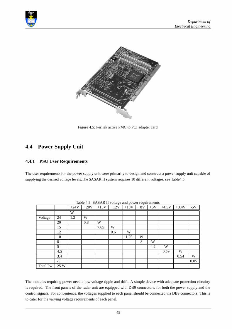
Department ofElectrical Engineering
Figure 4.5: Peritek active PMC to PCI adapter card
4.4 Power Supply Unit
4.4.1 PSU User Requirements
The user requirements for the power supply unit were primarily to design and construct a power supply unit capable of
supplying the desired voltage levels.The SASAR II system requires 10 different voltages, see Table4.5:
Table 4.5: SASAR II voltage and power requirements+24V +20V +15V +12V +10V +8V +5V +4.5V +3.4V -5V
WVoltage 24 1.2 W
20 0.8 W15 7.65 W12 0.6 W10 1.25 W8 8 W5 4.2 W4.5 0.59 W3.4 0.54 W-5 0.05
Total Pw 25 W
The modules requiring power need a low voltage ripple and drift. A simple device with adequate protection circuitry
is required. The front panels of the radar unit are equipped with DB9 connectors, for both the power supply and the
control signals. For convenience, the voltages supplied toeach panel should be connected via DB9 connectors. This is
to cater for the varying voltage requirements of each panel.
45
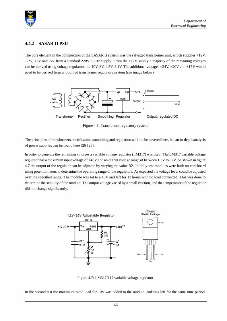
Department ofElectrical Engineering
4.4.2 SASAR II PSU
The core element in the construction of the SASAR II system was the salvaged transformer unit, which supplies +12V,
-12V, +5V and -5V from a standard 220V/50 Hz supply. From the +12V supply a majority of the remaining voltages
can be derived using voltage regulators i.e. 10V, 8V, 4.5V, 3.4V. The additional voltages +24V, +20V and +15V would
need to be derived from a modified transformer regulatory system (see image below) .
Figure 4.6: Transformer regulatory system
The principles of transformers, rectification, smoothing and regulation will not be covered here, but an in-depth analysis
of power supplies can be found here [26][28].
In order to generate the remaining voltages a variable voltage regulator (LM317) was used. The LM317 variable voltage
regulator has a maximum input voltage of +40V and an output voltage range of between 1.3V to 37V. As shown in figure
4.7 the output of the regulator can be adjusted by varying thevalue R2. Initially test modules were built on veri-board
using potentiometers to determine the operating range of the regulators. As expected the voltage level could be adjusted
over the specified range. The module was set to a 10V and left for 12 hours with no load connected. This was done to
determine the stability of the module. The output voltage varied by a small fraction, and the temperature of the regulator
did not change significantly.
Figure 4.7: LM317/117 variable voltage regulator
In the second test the maximum rated load for 10V was added to the module, and was left for the same time period.
46

Department ofElectrical Engineering
The addition of the load caused the output voltage to degradeby a substantial amount, almost 20% of the rated voltage.
The temperature of the module had also dramatically increased. During testing it was verified that the potentiometer
was also mechanically unstable, sharp movements cause the set resistance value to change. It was concluded that the
vibrations from the aircraft may cause the regulated voltage to shift.
4.5 Conclusions
The 19 inch temporary housing rack was constructed using wood. The lack of a solid ground may lead to signal
referencing errors in later stages of the transceiver.
The initial design of the PSU had all the voltage modules mounted on one piece of veri board. This method of construc-
tion failed to adequately cater for over current protection. If one voltage regulator module was damaged the required
time for repair would be almost 2 hours.
A modular design was opted for the second version, which involved building each voltage module onto a separate piece
of veri-board with an input fuse protection. Using a voltageindicator LED on the front panel for each voltage, the user
can identify where the problem may be. This significantly reduces the time required to fix the problem. Each voltage is
colour coded and only the required voltages are distributedto the DB9 connectors on the front panel of the PSU.
47

Chapter 5
Subsystem Testing
In a system each component in a signal chain must receive the proper signal level from the previous component in order
to output the correct power level to the succeeding component. If the output power level is too low, the signal can be
obscured in noise. If the power level becomes too high, the performance of the device becomes nonlinear and distortion
occurs. A worse case scenario is driving a component beyond its capabilities resulting in its permanent damage.
The successful construction of the Housing unit and the power supply make it easier to perform the basic system veri-
fication tests. As far as possible the tests performed recreated the original testing conditions as detailed in [4][12][15].
These tests were divided into four stages:
• FDU testing: to verify the frequencies and power levels of the local oscillators
• RDU testing: Outputting and sampling the I and Q chirp waveforms
• Transmitter testing: tracking of waveform through variousstages to verify power levels
• Receiver testing: performing manual loop back testing to ensure proper down conversion of signals
Since the power supply unit was loaded and tested rigorously, the initial verification test was ensure that the RF modules
were being supplied with the correct voltages. A table of thefront panel voltages can be found in Appendix A.
The testing methods and the use of specialized testing equipment are detailed in Appendix C, with particular reference
to [24][23][22][25][19].
It must be noted that during most of the original testing procedures by [4][12][15] there was insufficient testing equip-
ment. There was substantially more equipment made available during the integrated testing of the SASAR II system.
Therefore the results produced during the following tests were not picked up during the original tests.
5.1 FDU Testing
The tests performed on the FDU are to determine the center frequency and the power level of the LO signals. If the
power level is too low, the mixers will be insufficiently driven and the output signal will not be generated. Should the
48

Department ofElectrical Engineering
LO power level be too high the mixers will be driven into saturation causing intermodulation harmonic distortion. All
the clocking and LO frequencies are due to be derived from a 10MHz stable crystal oscillator. The use of a common 10
MHz stable oscillator ensures coherency in later stages of the transceiver. For testing purposes the 10 MHz reference
signal is supplied by an Hp 8635 arbitrary waveform generator. The 10 MHz signal is then split and distributed to the
five frequency sysnthesizers. At this phase of testing the RCU as described in 4.2.1 was unavailable. The windows
based programmer, CodeLoader2, was then opted for.
5.1.1 Testing Methodology
The synthesizers are programmed via a 16 bit serial data stream from the parallel port of the host machine from the win-
dows based Code-loader2 program. The current method of programming the frequency synthesisers is by the supplied
windows based Code-loader2 program, that sends out a bit stream of data via the computers parallel port and interfaces
with the synthesiser via a DB9 connector on the front panel ofthe housing unit. The frequency counter, as described in
3.2, divides the 10 MHz crystal reference in order to generate the desired frequency. The test setup is shown below.
Figure 5.1: FDU testing setup
The output of the synthesizers are measured using the spectrum analyzer. Since the waveform generated is a continuous
wave (CW), there is no need to apply the PDF.
The factors considered when testing the FDU were:
• Input reference power level: a weak signal would fail to trigger the frequency counter/multiplier (min 3 dBm)
• Frequency stability: an unstable signal would affect the coherency of the system
49

Department ofElectrical Engineering
• Output power level: a high power level would drive the mixer into saturation causing intermodulation products
(max 7 dBm)
5.1.2 Results and Analysis
The table below shows the FDU testing results with emphsis on:
• Frequency
• Output power
• Input device
• Variance between minimu power required, 3 dBm, and maximum power allowable
Table 5.1: FDU LO power levels
Frequency Part Number Output Pw Pw after amplifier Input to device LO max Variance
158 MHz (I) SZ1 (SPLL-S-A40) 5.42 dBm 9.48 dBm MIX 1 +7 dBm +2.48 dB158 MHz (Q) SZ1 (SPLL-S-A40) 5.42 dBm 9.18 dBm MIX 2 +7 dBm +2.18 dB
1142 MHz (Tx) SZ2 (SPLH-S-A79) 4.7 dBm 8.76 dBm MIX 3 +7 dBm +1.76 dB1142 MHz (Rx) SZ2 (SPLH-S-A79) 4.7 dBm 10.61 dBm MIX 7 +7 dBm +3.61 dB
4000 MHz SZ3 (SPLH-S-4000F) 0.9 dBm 10.12 dBm FD (F15KXSP) +7 dBm +3.12 dB
8000 MHz (Tx) FD (F15KXSP) -19 dBm 4.18 dBm MIX 4 +7 dBm -3.18 dB
8000 MHz (Rx) FD (F15KXSP) -19 dBm 4.28 dBm MIX 4 +7 dBm -3.28 dB
150 MHz SZ4 (SPLL-S-A40) 4.28 dBm N/A DPG +5 dBm -0.72 dB
210 MHz SZ5 (SPLL-S-A40) 5.43 dBm N/A ADC +5 dBm +0.57 dB
5.1.3 Conclusion
The testing results shown in 5.1 closely matches the resultsachieved in [4]. The results demonstrate the degree to which
the mismatches would impact on the input devices in the latermodules.
To generate the 8 GHz LO signal, the output of the 4 GHz synthesizer is doubled and then amplified. The output of
the synthesizer is however too low to trigger the frequency doubler effectively. To compensate for this a 14.5 dB gain
amplifier (HMC 311LP3) from Hitite Microwave was used.
The ADC is specified to receive an input clocking frequency of210 MHz. This is however not the case, the ADC
samples channel A and B (I and Q) 180 degrees out of phase at 105MHz. Both channels are later combined in software
to achieve a final bandwidth of 210 MHz. The frequency synthesizer is only capable of frequency outputs from 150
MHz to 210 MHz. To obtain a frequency of 105 MHz using the original device, a Hitite Microwave HMC 432 divide
by two was used.
The LO signals at MIX1, MIX2, MIX3 and MIX7 are a minimum of 3 dBover the maximum input LO power. This
leads to a higher conversion loss of up to 1 dB and higher peak signal amplitudes of the harmonic signals.
50

Department ofElectrical Engineering
5.2 DPG Testing
The DPG was originally tested at Parsec by using a signal generator, spectrum analyzer, oscilloscope and compact PCI
rack. The control registers were tested individually, by writing and reading to registers. The output of the chirp signals
was not part of the original test procedure [15].
The DPG is connected to the PCI bus of the host machine using the Peritek passive adapter card. The external clock of
150MHz for the unit is supplied from the system’s FDU. The DPGis triggered by it’s internal clock. The DPG can be
triggered to output two signal formats, band-limited and not band-limited.
5.2.1 Band-Limit
A band-limited chirp signal has a fixed start and end point in the time domain. Although this is a practical consideration
in the time domain, the same signal when transposed to the frequency domain rolls off gradually towards zero. Without
stringent filtering this can lead to aliasing. Band-limiting is achieved by using windowing functions i.e. Hanning,
Hamming windows etc.
Figure 5.2: Time domain band-limiting using window functions
51

Department ofElectrical Engineering
Figure 5.3: Frequency domain band-limiting
5.2.2 No Band-Limit
A non band-limited chirp signal is the converse of the band-limited signal; no windowing function has been applied to
it in the time domain. In the frequency domain the signal walls run steeply towards zero.
Figure 5.4: Time domain based signal with no band-limiting
52

Department ofElectrical Engineering
Figure 5.5: Frequency domain signal with no band-limiting
5.2.3 Conclusion
The output power of the DAC, according to the manufacturers specifications is 0 dBm. This differs from the specified
output power of +10 dBm. The main lobe amplitude of the DPG output shown in 5.3, is -3.402 dBm. The peak pulse
power of the signal is therefore, -3.402 dBm + 3.52 dB (PDF) = 0.118 dBm. The RF power levels calculated in 5.4 were
made using the peak pulse output power of 0 dBm. S
5.3 ADC Testing
The original testing of the SU at Parsec was not completed dueto the lack of test equipment. To fully test the SU,
two signal generators were required; Parsec however only had one high quality signal generator, which was used as the
input signal. The SU was clocked using its onboard 30 MHz clock. To test the SU correctly it should have been clocked
around 105 MHz, as this was the required input clock frequency [15].
During the full integrated system testing of the ADC (at 105 MHz), the channel B input would drop some samples (see
5.6)
53

Department ofElectrical Engineering
Figure 5.6: Original test results of (a) Channel A (b) Channel B (c) Frequency Spectrum (d) A and B combined
The initial theory was was that the modification made to allowthe channels to be sampled at 105 MHz and 180 degrees
out of phase may have corroded, resulting in timing errors. This however was deemed improbable as the final tests
conducted in [15] proved the system was operational. Recreating the original test conditions revealed that the ADC
was used with the Peritek passive PCI adapter card (see 4.3.1) , with the input test signals from an arbitrary waveform
generator. Under the current test conditions, the card was being operated at 66 MHz (PMC core) to 33 MHz (PCI core)
at 64bits using the active card. The timing inaccuracies between the two cores caused by the jumper settings may have
resulted in the ADC dropping some samples.
In order to verify the source of the problems numerous tests were conducted using the available hardware. The tests
were divided into the following categories:
• DPG on passive card (clocked externally 150 MHz), ADC on active card (clocked externally 105 MHz)
• DPG on active card (clocked externally 150 MHz), ADC on passive card (clocked externally 105 MHz)
• DPG on passive card (clocked externally), ADC on active card(clocked externally 105 MHz: clock jumpers on
active card were changed)
• DPG on passive card (clocked externally), ADC on active card(clocked externally in frequency steps of 10 MHz
from 60 MHz to 100 MHz and 105 MHz).
54
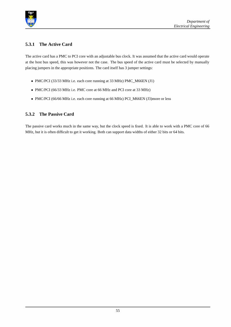
Department ofElectrical Engineering
5.3.1 The Active Card
The active card has a PMC to PCI core with an adjustable bus clock. It was assumed that the active card would operate
at the host bus speed, this was however not the case. The bus speed of the active card must be selected by manually
placing jumpers in the appropriate positions. The card itself has 3 jumper settings:
• PMC/PCI (33/33 MHz i.e. each core running at 33 MHz) PMC_M66EN (J1)
• PMC/PCI (66/33 MHz i.e. PMC core at 66 MHz and PCI core at 33 MHz)
• PMC/PCI (66/66 MHz i.e. each core running at 66 MHz) PCI_M66EN (J3)more or less
5.3.2 The Passive Card
The passive card works much in the same way, but the clock speed is fixed. It is able to work with a PMC core of 66
MHz, but it is often difficult to get it working. Both can support data widths of either 32 bits or 64 bits.
55

Department ofElectrical Engineering
5.3.3 Testing Methodology
The test setup was connected as shown in the diagram given below:
Figure 5.7: RDU test setup
The signal generator increased the noise floor by almost 20 dB. The LO power level was set at 4 dBm. The input signal
to the ADC was looped back directly from the DPG using SMB maleto male cables. The signal transmitted from the
DPG was sampled and stored in a binary file for post processingusing MATLAB.
5.3.4 Test Results
5.3.4.1 DPG on passive card, ADC on active card (clocked externally 105 MHz)
see figure 5.6
56

Department ofElectrical Engineering
5.3.4.2 DPG on active card, ADC on passive card (clocked externally 105 MHz)
Figure 5.8: PMC adapter cards swapped (a) Channel A (b) Channel B (c) Frequency Spectrum (d) A and B combined
57
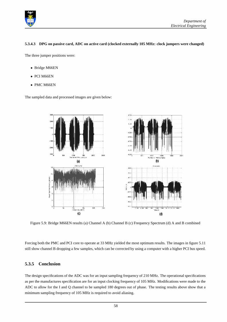
Department ofElectrical Engineering
5.3.4.3 DPG on passive card, ADC on active card (clocked externally 105 MHz: clock jumpers were changed)
The three jumper positions were:
• Bridge M66EN
• PCI M66EN
• PMC M66EN
The sampled data and processed images are given below:
Figure 5.9: Bridge M66EN results (a) Channel A (b) Channel B (c) Frequency Spectrum (d) A and B combined
Forcing both the PMC and PCI core to operate at 33 MHz yielded the most optimum results. The images in figure 5.11
still show channel B dropping a few samples, which can be corrected by using a computer with a higher PCI bus speed.
5.3.5 Conclusion
The design specifications of the ADC was for an input samplingfrequency of 210 MHz. The operational specifications
as per the manufactures specification are for an input clocking frequency of 105 MHz. Modifications were made to the
ADC to allow for the I and Q channel to be sampled 180 degrees out of phase. The testing results above show that a
minimum sampling frequency of 105 MHz is required to avoid aliasing.
58

Department ofElectrical Engineering
Figure 5.10: PCI M66EN results (a) Channel A (b) Channel B (c)Frequency Spectrum (d) A and B combined
Figure 5.11: PMC M66EN results (a) Channel A (b) Channel B (c)Frequency Spectrum (d) A and B combined
59

Department ofElectrical Engineering
A PCI bus speed of 33 MHz is insufficient to handle the data rates achieved by the ADC. The passive PMC adapter card
is equally incapable of handling the data rates, hence the dropped samples. The ADC is operational when used with the
PMC active adapter with the core speed forced to the PCI bus speed of 33 MHz. For long term sampling purposes the
number of range bins may have to be reduced from 8192, to 4096 to accommodate the slower PCI bus speed.
The DPG can be operated on either the active or the passive PMCadapter card.
5.4 Transmitter Testing
Having tested the FDU and ensuring that all LO power levels are within the operating levels of the mixers, the next
stage is to test that the transmitter is operating within thedesign specifications. The transmitter is divided into 3 main
sections, namely:
1. The 1stIF (158 MHz)
2. The 2ndIF (1300 MHz)
3. The 3rdIF or RF (9300 MHz)
The tests for each section are performed on a component levelto verify the design specifications of the transmitter.
5.4.1 Equipment Used and Testing Methodology
The equipment used in the testing are:
• DAC (DPG)
• ADC (SU)
• SASAR II power supply
• Spectrum Analyser - Agilent 9 kHz - 26.5 GHz E4470B
• Oscilloscope - Tektronik
• Sweep Oscillator - HP 8350
• Attenuators - 1 - 20dB barrel attenuators
The SASAR II is a pulsed RF system, with an adjustable PRF of 1.85 kHz to 3.1 kHz. As described in [Appendix
C], a factor to consider when making pulsed RF measurements is the distribution of the output power over the spectral
components lowers the peak pulse power. To compensate for the distribution of the power over the spectral components,
the pulse desensitisation factor (PDF) must be taken into consideration. The PDF is a function of duty cycle and is
represented by 20log(duty cycle). The pulse width of the transmitted chirp signal is5µs, with a period of7.5µs, giving
a duty cycle of 0.67. The PDF of the system is then:
60
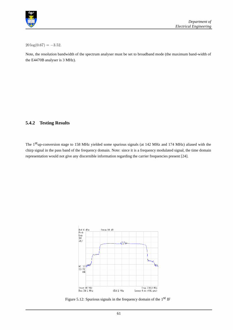
Department ofElectrical Engineering
20 log(0.67) = −3.52.
Note, the resolution bandwidth of the spectrum analyser must be set to broadband mode (the maximum band-width of
the E4470B analyser is 3 MHz).
5.4.2 Testing Results
The 1stup-conversion stage to 158 MHz yielded some spurious signals (at 142 MHz and 174 MHz) aliased with the
chirp signal in the pass band of the frequency domain. Note: since it is a frequency modulated signal, the time domain
representation would not give any discernible informationregarding the carrier frequencies present [24].
Figure 5.12: Spurious signals in the frequency domain of the1st IF
61

Department ofElectrical Engineering
Figure 5.13: Spurious signals at 142 MHz and 174 MHz with IF signal at 158 MHz
Further investigation revealed that the two spurious frequencies were the products of multiples of the DPG clocking
frequency of 150 MHz and the 1st IF LO of 158 MHz.
• (2 X 150 MHz) - 158 MHz = 142 MHz
• (3 X 158 MHz) - (2 X 150 MHz) = 174 MHz
The specified port to port isolation of the DPG is stated at 60 dB. The 150 MHz harmonics leak through with a power
level of -52 dBm. Using a low pass filter on both I and Q channelsof the DPG the harmonics of the 150 MHz clocking
frequency can be removed.
62

Department ofElectrical Engineering
Figure 5.14: I and Q low pass filter S21test
Figure 5.15: 1st IF with spurious signals filtered out
Using appropriate attenuators, the power levels of each component is measured and recorded using the spectrum
analyser. For convenience the power levels of each component are displayed in graphical form shown in 5.18,5.19,5.20.
63

Department ofElectrical Engineering
Figure 5.16: DPG output
Figure 5.17: RF (9300 MHz) output
64
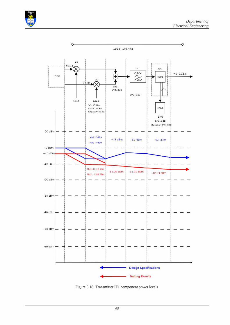
Department ofElectrical Engineering
Figure 5.18: Transmitter IF1 component power levels
65

Department ofElectrical Engineering
Figure 5.19: Transmitter IF2 component power levels
66

Department ofElectrical Engineering
Figure 5.20: Transmitter RF component power levels
67

Department ofElectrical Engineering
5.4.3 Conclusions
From the tests conducted on the transmitter we can conclude that:
• The peak pulse power of the final transmit RF signal is 8.602 dBm (5.087 dBm + 3.52 dB). This is however much
less than the expected power level of 18.9 dBm with the difference being 10.293 dBm. This loss can be attributed
to:
• A loss of 3 dB through SP1, instead of a summing gain of 3 dB.
• A high conversion loss of 7 dB through M4.
• Cable losses
The peak power of the final RF signal can be amplified at the end of the 1stIF stage with a standard 10 dB - 15 dB
amplifier. The results of this will be discussed in the conclusions and recommendations chapter.
5.5 Receiver Testing
Having tested the transmitter and ensuring that all power levels are within the design specifications, the next stage is
to verify that the receiver is operating within its design specifications. The receiver is divided into 4 main sections,
namely:
1. The 1st IF or RF (9300 MHz)
2. The 2ndIF (1300 MHz)
3. The 3rdIF, STC (158 MHz)
4. MGC (158 MHz)
The tests for each section are performed on a component levelto verify the design specifications of the receiver.
5.5.1 Equipment Used and Methodology
The equipment used in the testing are:
• SASAR II power supply
• Spectrum Analyser - Agilent 9 kHz - 26.5 GHz E4470B
• Oscilloscope - Tektronik
• Sweep Oscillator - HP 8350
• Attenuators - 1 dB - 20 dB barrel attenuators
68

Department ofElectrical Engineering
The testing of the receiver follows much the same methodology as that of the transmitter, in the respect that the power
levels of each individual component is recorded in order to verify the design specifications. The received signal is
however sampled and digitized for post processing as described in 2.5.
5.5.2 RF Testing Results
The maximum input power level to the spectrum analyser is +30dBm. Great care must be taken to ensure that the
power levels do not exceed this value. To prevent this, a highpower 20 dB attenuator is used at the input of the analyser,
in addition to the DC block.
Figure 5.21: Receiver input signal
69
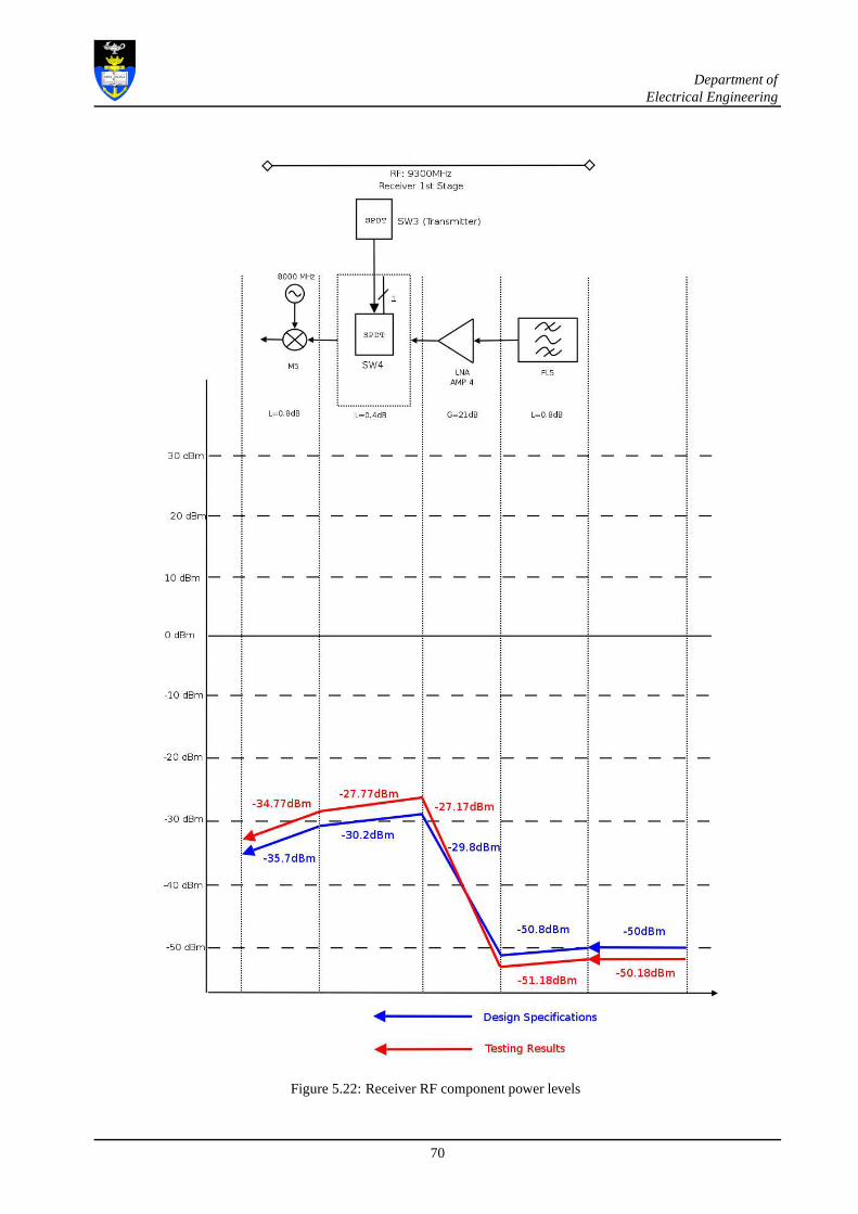
Department ofElectrical Engineering
Figure 5.22: Receiver RF component power levels
70
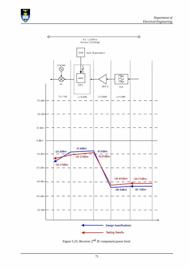
Department ofElectrical Engineering
Figure 5.23: Receiver 2nd IF component power level
71
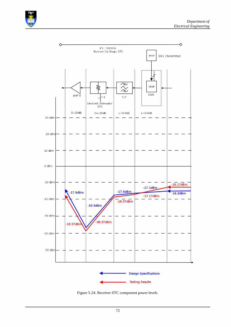
Department ofElectrical Engineering
Figure 5.24: Receiver STC component power levels
72
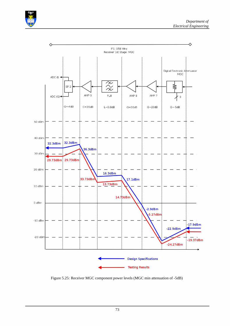
Department ofElectrical Engineering
Figure 5.25: Receiver MGC component power levels (MGC min attenuation of -5dB)
73

Department ofElectrical Engineering
Figure 5.26: Receiver MGC component power levels (MGC max attenuation of -35dB)
74

Department ofElectrical Engineering
5.5.3 ADC Sampling Results
The ADC sampling tests are done to verify that the received signal can be sampled, processed and then stored. The
sampling process makes use of the PM480 ADC card clocked by the 105 MHz clock pulse.
5.5.3.1 1st Test
Figure 5.27: Sampled chirp waveform
75

Department ofElectrical Engineering
Figure 5.28: Down-converted chirp waveform
76

Department ofElectrical Engineering
Figure 5.29: Time domain focused signal
77
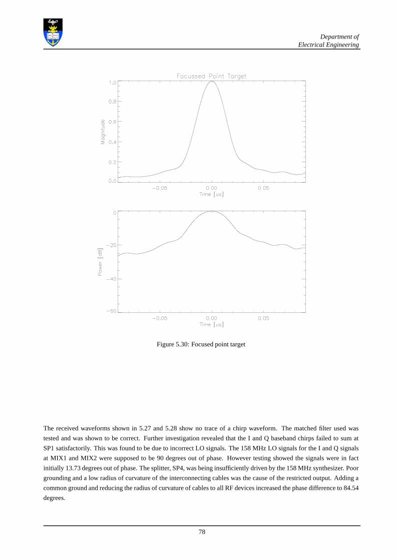
Department ofElectrical Engineering
Figure 5.30: Focused point target
The received waveforms shown in 5.27 and 5.28 show no trace ofa chirp waveform. The matched filter used was
tested and was shown to be correct. Further investigation revealed that the I and Q baseband chirps failed to sum at
SP1 satisfactorily. This was found to be due to incorrect LO signals. The 158 MHz LO signals for the I and Q signals
at MIX1 and MIX2 were supposed to be 90 degrees out of phase. However testing showed the signals were in fact
initially 13.73 degrees out of phase. The splitter, SP4, wasbeing insufficiently driven by the 158 MHz synthesizer. Poor
grounding and a low radius of curvature of the interconnecting cables was the cause of the restricted output. Adding a
common ground and reducing the radius of curvature of cablesto all RF devices increased the phase difference to 84.54
degrees.
78

Department ofElectrical Engineering
Figure 5.31: LO signals for 1st IF (13.73o)
Figure 5.32: LO signals for 1st IF (84.54o)
79

Department ofElectrical Engineering
5.5.3.2 No Band Limiting
Figure 5.33: Sampled chirp waveform
80

Department ofElectrical Engineering
Figure 5.34: Down-converted chirp waveform
81

Department ofElectrical Engineering
Figure 5.35: Time domain focused signal
82
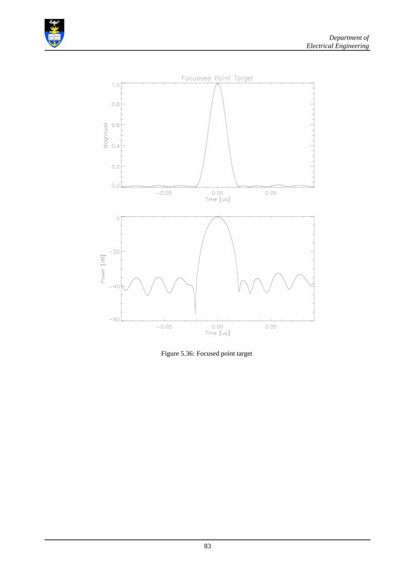
Department ofElectrical Engineering
Figure 5.36: Focused point target
83

Department ofElectrical Engineering
5.5.3.3 Band Limited
Figure 5.37: Sampled chirp waveform
84
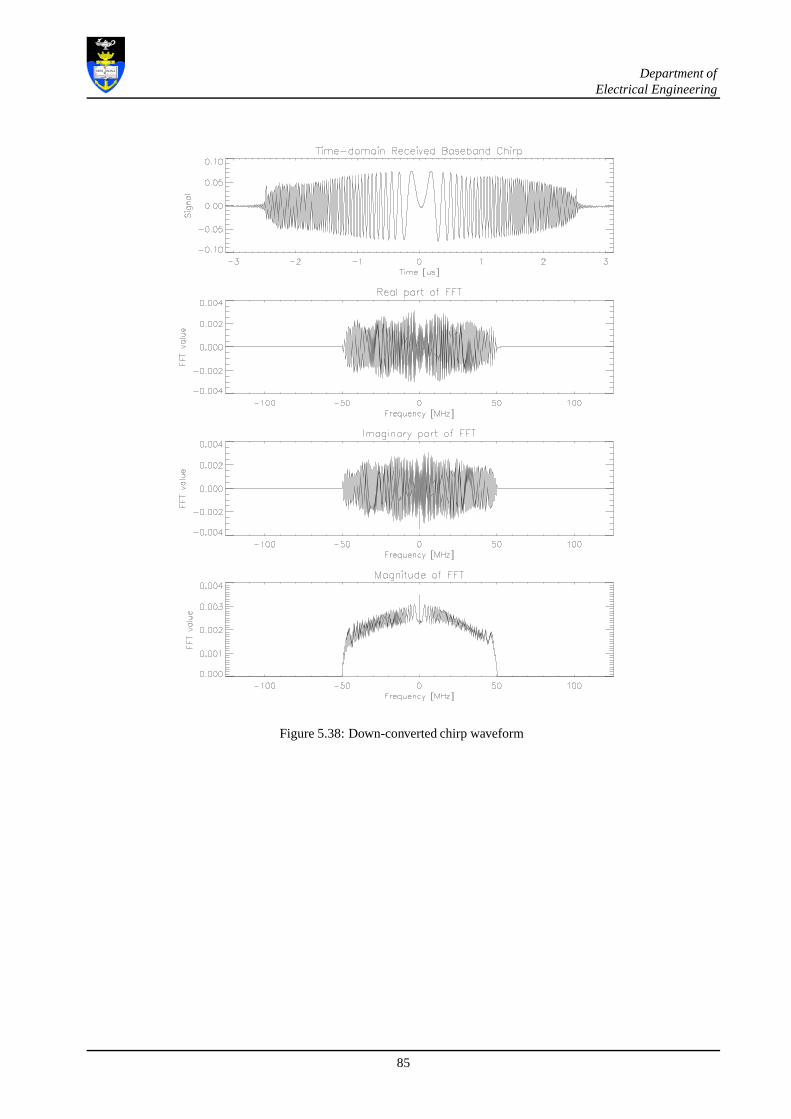
Department ofElectrical Engineering
Figure 5.38: Down-converted chirp waveform
85
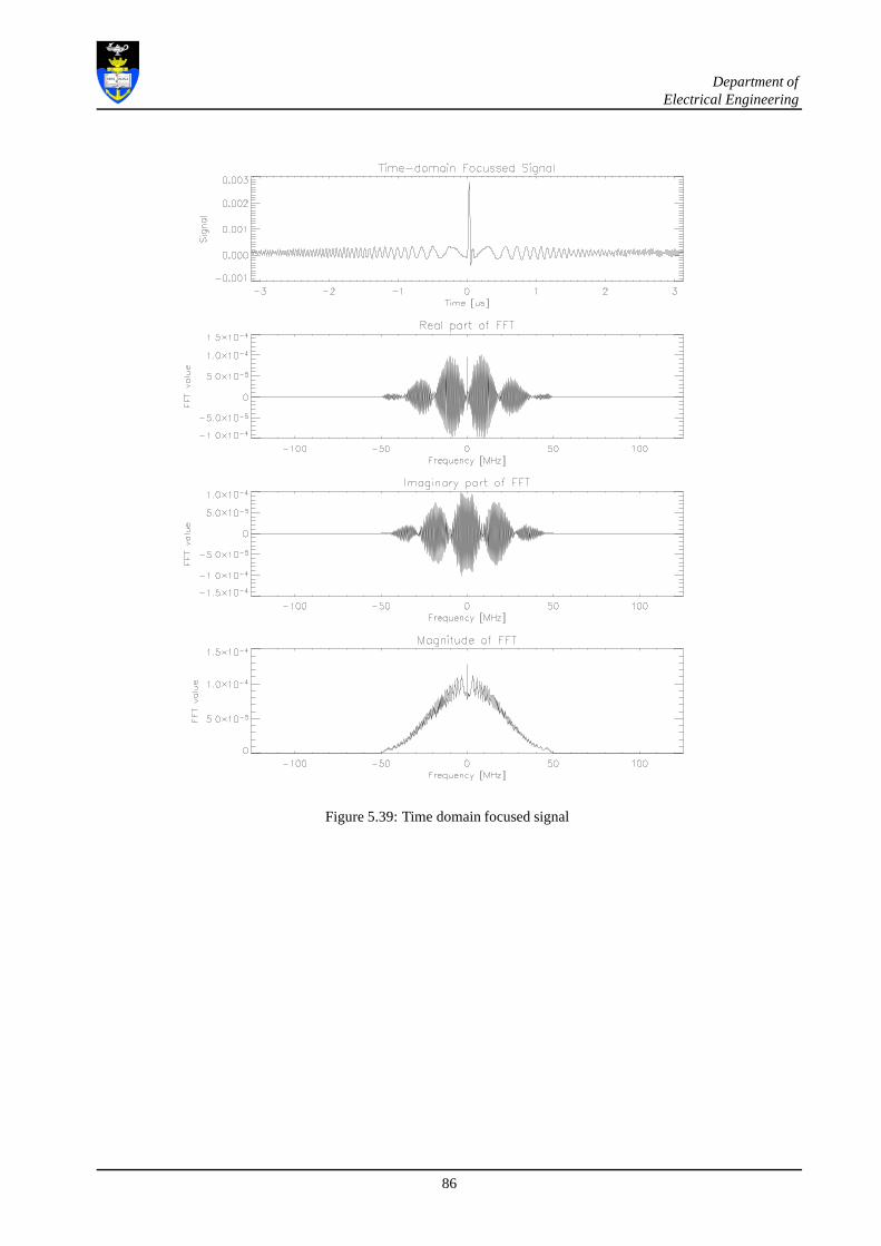
Department ofElectrical Engineering
Figure 5.39: Time domain focused signal
86
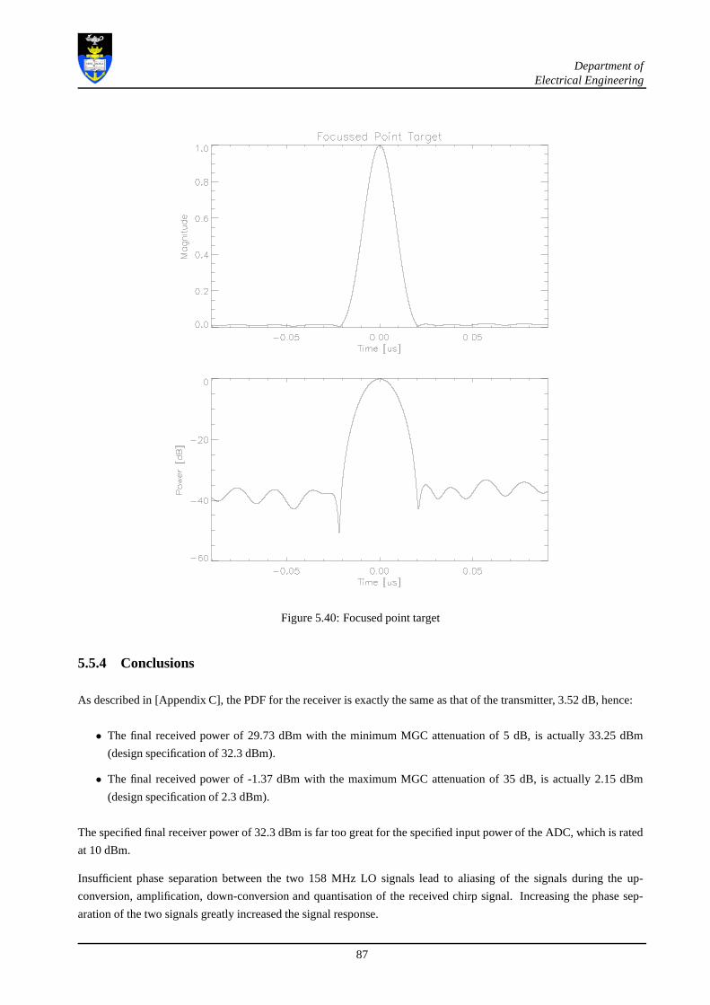
Department ofElectrical Engineering
Figure 5.40: Focused point target
5.5.4 Conclusions
As described in [Appendix C], the PDF for the receiver is exactly the same as that of the transmitter, 3.52 dB, hence:
• The final received power of 29.73 dBm with the minimum MGC attenuation of 5 dB, is actually 33.25 dBm
(design specification of 32.3 dBm).
• The final received power of -1.37 dBm with the maximum MGC attenuation of 35 dB, is actually 2.15 dBm
(design specification of 2.3 dBm).
The specified final receiver power of 32.3 dBm is far too great for the specified input power of the ADC, which is rated
at 10 dBm.
Insufficient phase separation between the two 158 MHz LO signals lead to aliasing of the signals during the up-
conversion, amplification, down-conversion and quantisation of the received chirp signal. Increasing the phase sep-
aration of the two signals greatly increased the signal response.
87

Department ofElectrical Engineering
Stringent filtering in software negated the effects of aliasing when using the band-limited signals.
The performance of the STC on the system could not be verified as the RCU had not been programmed to output the
time based attenuation levels. As a result the STC was set to its maximum level of attenuation at -20 dBm.
88

Chapter 6
Conclusions
6.1 System Integration
The use of wood for the 19 inch rack led to frequency instability of the frequency synthesizers and an insufficient phase
offset of the waveform splitter.
The initial design of the PSU had all the voltage modules mounted on one piece of veri board. This method of construc-
tion failed to adequately cater for over current protection. If one voltage regulator module was damaged the required
time for repair would be almost 2 hours. A modular design and input fuse protection greatly reduced the total down
time of the system.
6.2 Subsystem Testing
6.2.1 FDU Testing
To generate the 8 GHz LO signal, the output of the 4 GHz synthesizer is doubled and then amplified. The output of
the synthesizer is however too low to trigger the frequency doubler effectively. To compensate for this a 14.5 dB gain
amplifier (HMC 311LP3) from Hitite Microwave was used.
The ADC is specified to receive an input clocking frequency of210 MHz. This is however not the case, the ADC
samples channel A and B (I and Q) 180 degrees out of phase at 105MHz. Both channels are later combined in software
to achieve a final bandwidth of 210 MHz. The frequency synthesizer is only capable of frequency outputs from 150
MHz to 210 MHz. To obtain a frequency of 105 MHz using the original device, a Hitite Microwave HMC 432 divide
by two was used.
The LO signals at MIX1, MIX2, MIX3 and MIX7 are a minimum of 3 dBover the maximum input LO power. This
leads to a higher conversion loss of up to 1 dB and higher peak signal amplitudes of the harmonic signals.
89

Department ofElectrical Engineering
6.2.2 DPG
The output power of the DAC, according to the manufacturers specifications is 0 dBm. This differs from the specified
output power of +10 dBm. The main lobe amplitude of the DPG output shown in 5.3, is -3.402 dBm. The peak pulse
power of the signal is therefore, -3.402 dBm + 3.52 dB (PDF) = 0.118 dBm. The RF power levels calculated in 5.4 were
made using the peak pulse output power of 0 dBm.
6.2.3 Transmitter
From the tests conducted on the transmitter we can conclude that:
• The peak pulse power of the final transmit RF signal is 8.607 dBm (5.087 dBm + 3.52 dB). This is however much
less than the expected power level of 18.9 dBm with the difference being 10.293 dBm This loss can be attributed
to:
• A loss of 3 dB through SP1, instead of a summing gain of 3 dB.
• A high conversion loss of 7 dB through M4.
• Cable losses
The peak power of the final RF signal can be amplified at the end of the 1stIF stage with a standard 10 dB - 15 dB
amplifier. The results of this will be discussed in the conclusions and recommendations.
6.2.4 Receiver
As described in [Appendix C], the PDF for the receiver is exactly the same as that of the transmitter, 3.52 dBm, hence:
• The final received power of 29.73 dBm with the minimum MGC attenuation of 5 dB, is actually 33.25 dBm
(design specification of 32.3 dBm).
• The final received power of -1.37 dBm with the maximum MGC attenuation of 35 dB, is actually 2.15 dBm(design
specification of 2.3 dBm).
The specified final receiver power of 32.3 dBm is far too great for the specified input power of the ADC, which is rated
at 10 dBm.
Insufficient phase separation between the two 158 MHz LO signals lead to aliasing of the signals during the up-
conversion, amplification, down-conversion and quantisation of the received chirp signal. Increasing the phase sep-
aration of the two signals greatly increased the signal response.
Stringent filtering in software negated the effects of aliasing when using the band-limited signals.
The performance of the STC on the system could not be verified as the RCU had not been programmed to output the
time based attenuation levels. As a result the STC was set to its maximum level of attenuation at -20 dBm.
90

Department ofElectrical Engineering
6.2.5 ADC
The design specifications of the ADC was for an input samplingfrequency of 210 MHz. The operational specifications
as per the manufactures specification are for an input clocking frequency of 105 MHz. Modifications were made to the
ADC to allow for the I and Q channel to be sampled 180 degrees out of phase. The testing results above show that a
minimum sampling frequency of 105 MHz is required to avoid aliasing.
A PCI bus speed of 33 MHz is insufficient to handle the data rates achieved by the ADC. The passive PMC adapter card
is equally incapable of handling the data rates, hence the dropped samples. The ADC is operational when used with the
PMC active adapter with the core speed forced to the PCI bus speed of 33 MHz. For long term sampling purposes the
number of range bins may have to be reduced from 8192, to 4096 to accommodate the slower PCI bus speed.
Figure 2.6 shows the expected focused signal results with time spacing of 0.04µs and first side lobes sitting at -40 dB.
The final integrated system focused results shows time spacing of 0.04µsand the first side lobes sitting at -38 dB
The DPG can be operated on either the active or the passive PMCadapter card.
91

Chapter 7
Recommendations
Based on the tests results and the conclusions drawn, the following recommendations are made:
7.1 SASAR II housing
A common ground between the PSU and the housing unit of SASAR II must be constructed to obviate referencing
errors of the FDU.
Front panels for the backing plates must be constructed using SMA female bulk-head connectors to minimize the radius
of curvature of the Q-flex cables, thereby reducing cable loses.
Integrate a cooling unit into the housing unit to keep the internal operating temperature constant. Devices such as mixers
and amplifiers are susceptible to changes in temperature resulting in increased conversion losses.
7.2 FDU
The table in 5.1 shows the input power levels of the LO signals. The mixers MIX1, MIX2, MIX3 and MIX 7 are at least
3 dB over the maximum input power levels. This leads to a higher conversion loss of up to 1 dB and higher peak signal
amplitudes of the harmonic signals.
It is recommended that the FDU be reconfigured to output lowersignal amplitudes below the specified +7 dBm level
to reduce intermodulation product distortion in later stages. Barrel attenuators can also be used to reduced the power
levels, but this would be a waste of resources and is not recommended.
The quadrature splitter, SP4, offsets the 158 MHz LO by a phase of 84.54 degrees. The discrepancy of 5.46 degrees
will lead to aliasing problems during the down-conversion and sampling of the received signal. It is recommended that
testing be conducted to determine the cause of this discrepancy and if need be to replace the RF unit.
92
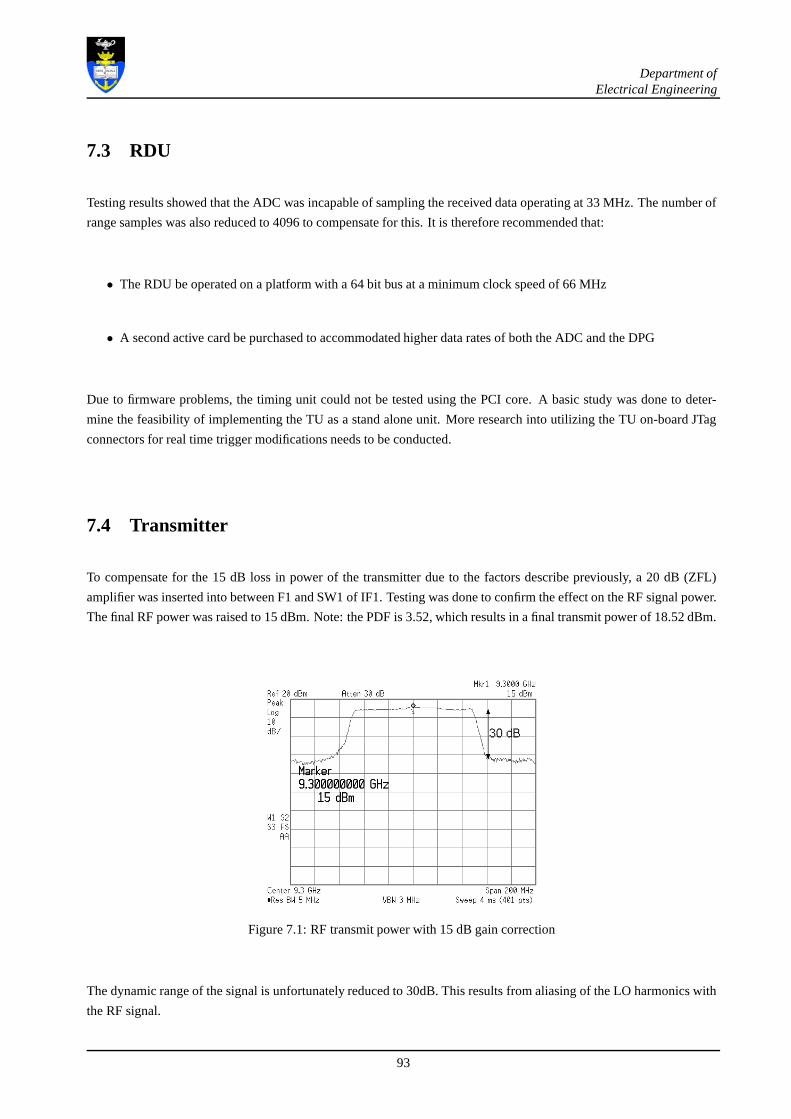
Department ofElectrical Engineering
7.3 RDU
Testing results showed that the ADC was incapable of sampling the received data operating at 33 MHz. The number of
range samples was also reduced to 4096 to compensate for this. It is therefore recommended that:
• The RDU be operated on a platform with a 64 bit bus at a minimum clock speed of 66 MHz
• A second active card be purchased to accommodated higher data rates of both the ADC and the DPG
Due to firmware problems, the timing unit could not be tested using the PCI core. A basic study was done to deter-
mine the feasibility of implementing the TU as a stand alone unit. More research into utilizing the TU on-board JTag
connectors for real time trigger modifications needs to be conducted.
7.4 Transmitter
To compensate for the 15 dB loss in power of the transmitter due to the factors describe previously, a 20 dB (ZFL)
amplifier was inserted into between F1 and SW1 of IF1. Testingwas done to confirm the effect on the RF signal power.
The final RF power was raised to 15 dBm. Note: the PDF is 3.52, which results in a final transmit power of 18.52 dBm.
Figure 7.1: RF transmit power with 15 dB gain correction
The dynamic range of the signal is unfortunately reduced to 30dB. This results from aliasing of the LO harmonics with
the RF signal.
93

Department ofElectrical Engineering
Figure 7.2: RF signal aliased with LO harmonics
The additional amplifier stage cannot be put before the first filtering stage, F1, as the LO and IF leakage from the mixers,
MIX1 and MIX2, would also be amplified.
Figure 7.3: IF and LO leakage at SP1
Based on the transfer function of the filter, the amplifier could not be put before the filter. The spurious harmonics
would also have been amplified making it difficult for the filter to reject the unwanted signals.
94
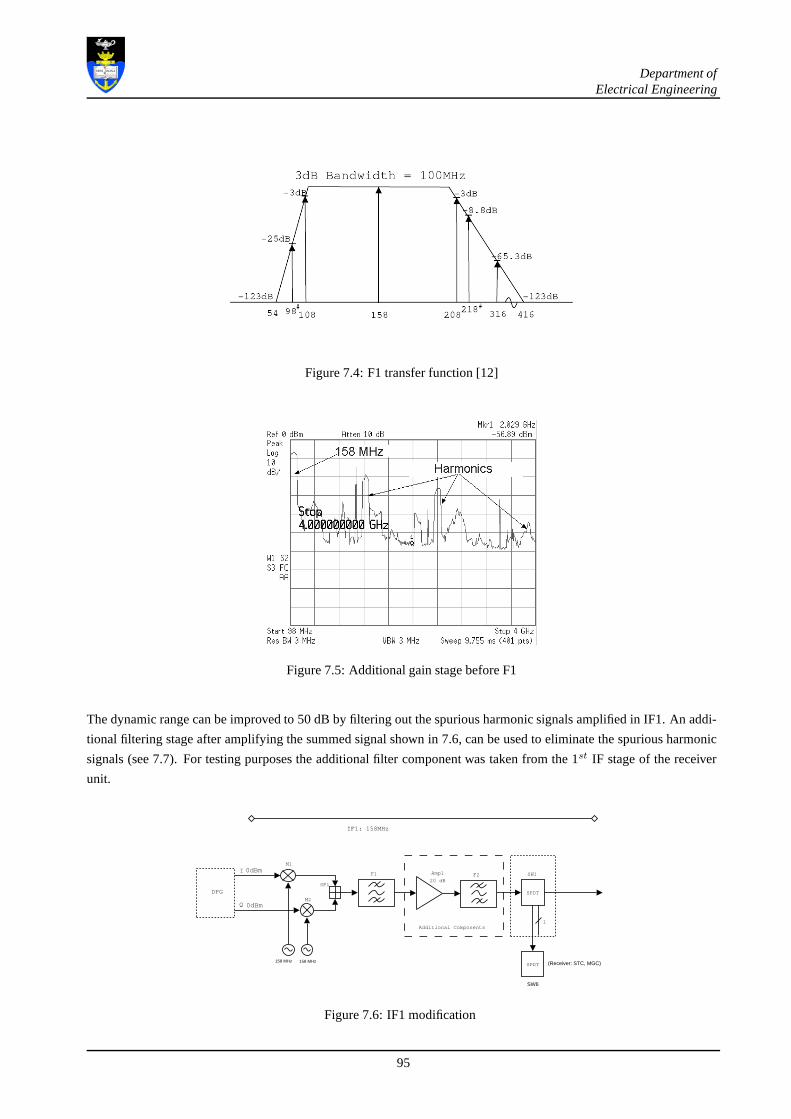
Department ofElectrical Engineering
Figure 7.4: F1 transfer function [12]
Figure 7.5: Additional gain stage before F1
The dynamic range can be improved to 50 dB by filtering out the spurious harmonic signals amplified in IF1. An addi-
tional filtering stage after amplifying the summed signal shown in 7.6, can be used to eliminate the spurious harmonic
signals (see 7.7). For testing purposes the additional filter component was taken from the 1st IF stage of the receiver
unit.
IF1: 158MHz
DPG
0dBm
0dBm
M1
M2
SP1
F1
SPDT
1
SW1
SW6
SPDT (Receiver: STC, MGC)
I
Q
158 MHz 158 MHz
F2Amp1
20 dB
Additional Components
Figure 7.6: IF1 modification
95
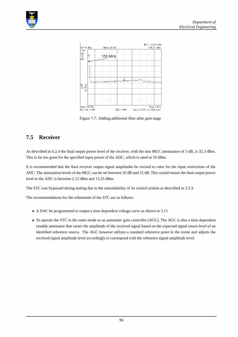
Department ofElectrical Engineering
Figure 7.7: Adding additional filter after gain stage
7.5 Receiver
As described in 6.2.4 the final output power level of the receiver, with the min MGC attenuation of 5 dB, is 32.3 dBm.
This is far too great for the specified input power of the ADC, which is rated at 10 dBm.
It is recommended that the final receiver output signal amplitudes be revised to cater for the input restrictions of the
ADC. The attenuation levels of the MGC can be set between 35 dBand 15 dB. This would ensure the final output power
level to the ADC is between 2.15 dBm and 13.25 dBm.
The STC was bypassed during testing due to the unavailability of its control system as described in 3.3.3.
The recommendations for the refinement of the STC are as follows:
• A DAC be programmed to output a time dependent voltage curve as shown in 3.11
• To operate the STC in the same mode as an automatic gain controller (AGC). The AGC is also a time dependent
tunable attenuator that varies the amplitude of the received signal based on the expected signal return level of an
identified reference source. The AGC however utilizes a standard reference point in the scene and adjusts the
received signal amplitude level accordingly to correspondwith the reference signal amplitude level.
96

Appendix A
Power Supply Unit
97

Department ofElectrical Engineering
Power Supply Unit documentation
This section serves to give the user an overview of the layoutof the SASAR II PSU.
Figure 8: SASAR II PSU front panel and voltage colour codes
98

Appendix B
SASAR II FDU
99
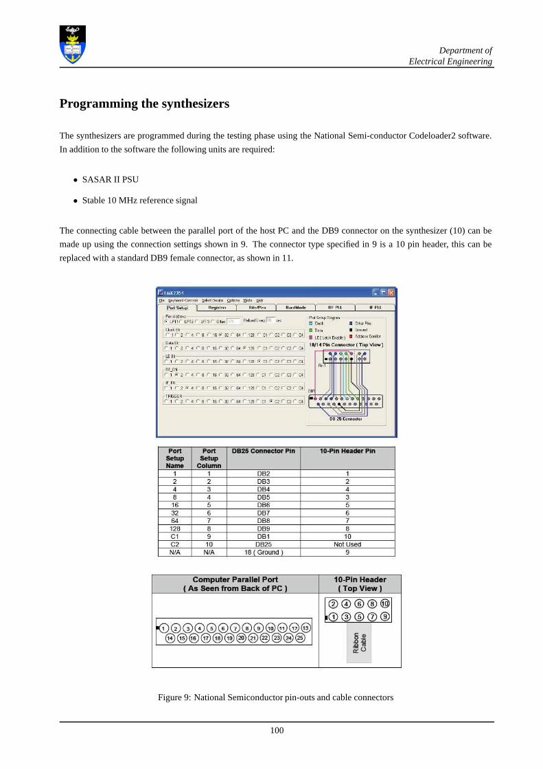
Department ofElectrical Engineering
Programming the synthesizers
The synthesizers are programmed during the testing phase using the National Semi-conductor Codeloader2 software.
In addition to the software the following units are required:
• SASAR II PSU
• Stable 10 MHz reference signal
The connecting cable between the parallel port of the host PCand the DB9 connector on the synthesizer (10) can be
made up using the connection settings shown in 9. The connector type specified in 9 is a 10 pin header, this can be
replaced with a standard DB9 female connector, as shown in 11.
Figure 9: National Semiconductor pin-outs and cable connectors
100
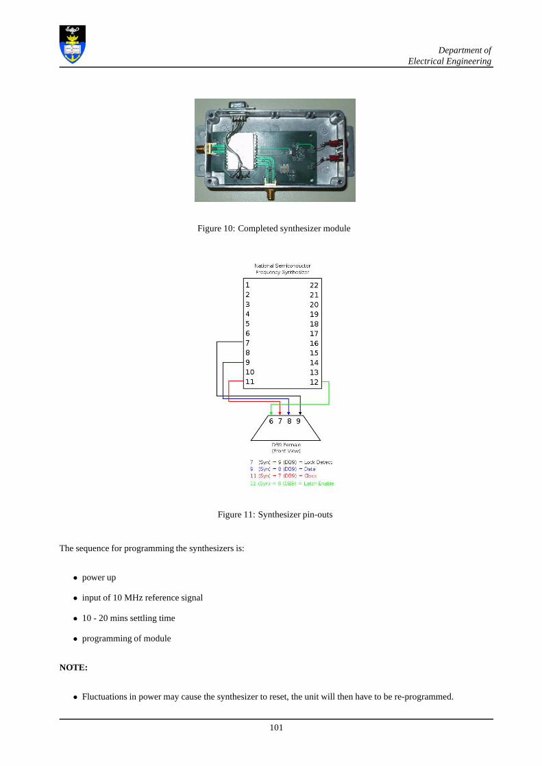
Department ofElectrical Engineering
Figure 10: Completed synthesizer module
Figure 11: Synthesizer pin-outs
The sequence for programming the synthesizers is:
• power up
• input of 10 MHz reference signal
• 10 - 20 mins settling time
• programming of module
NOTE:
• Fluctuations in power may cause the synthesizer to reset, the unit will then have to be re-programmed.
101
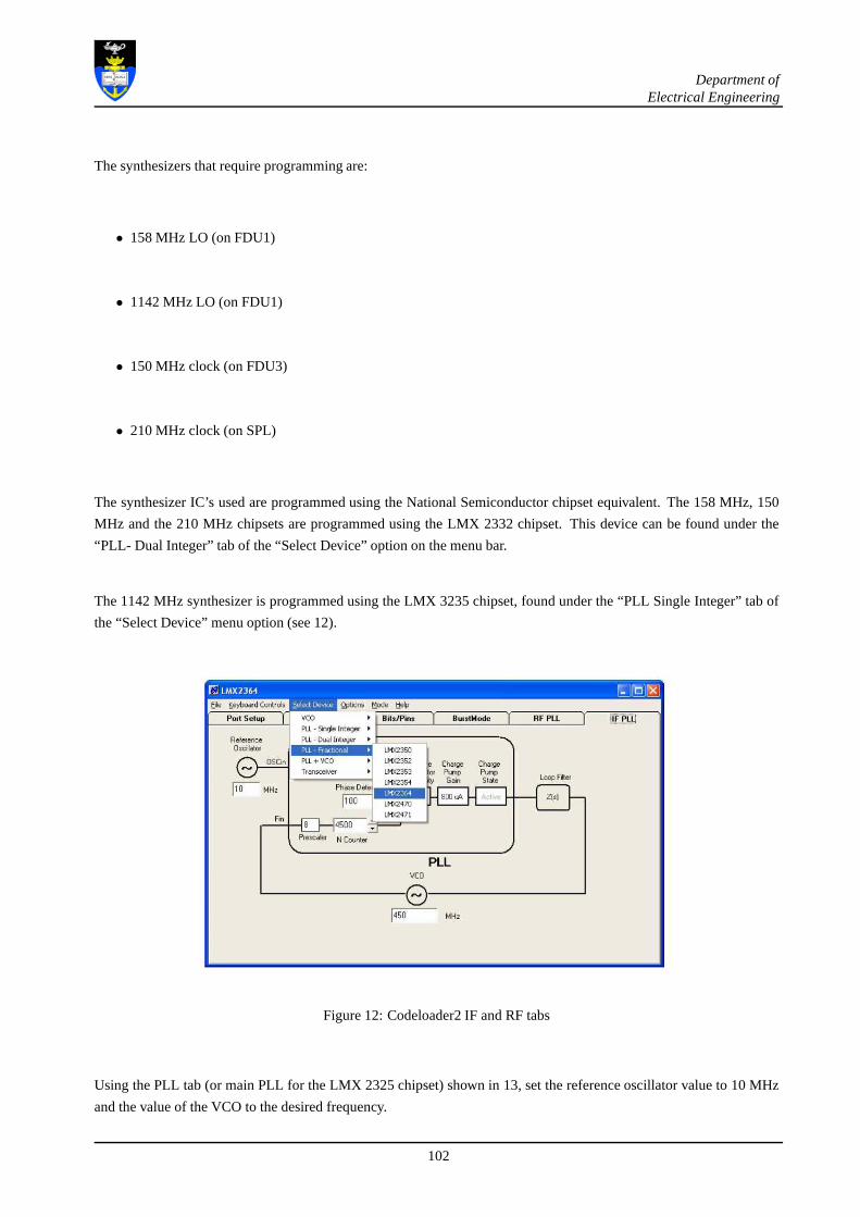
Department ofElectrical Engineering
The synthesizers that require programming are:
• 158 MHz LO (on FDU1)
• 1142 MHz LO (on FDU1)
• 150 MHz clock (on FDU3)
• 210 MHz clock (on SPL)
The synthesizer IC’s used are programmed using the NationalSemiconductor chipset equivalent. The 158 MHz, 150
MHz and the 210 MHz chipsets are programmed using the LMX 2332chipset. This device can be found under the
“PLL- Dual Integer” tab of the “Select Device” option on the menu bar.
The 1142 MHz synthesizer is programmed using the LMX 3235 chipset, found under the “PLL Single Integer” tab of
the “Select Device” menu option (see 12).
Figure 12: Codeloader2 IF and RF tabs
Using the PLL tab (or main PLL for the LMX 2325 chipset) shown in 13, set the reference oscillator value to 10 MHz
and the value of the VCO to the desired frequency.
102
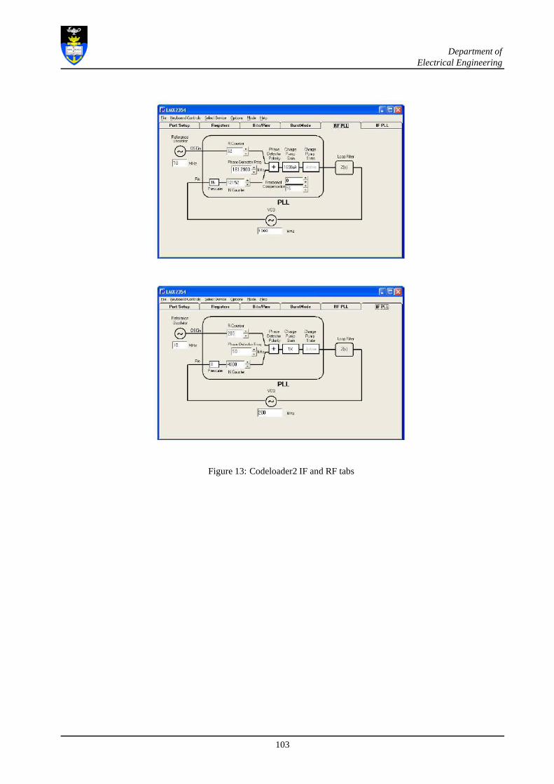
Department ofElectrical Engineering
Figure 13: Codeloader2 IF and RF tabs
103

Appendix C
Types of power measurements
104
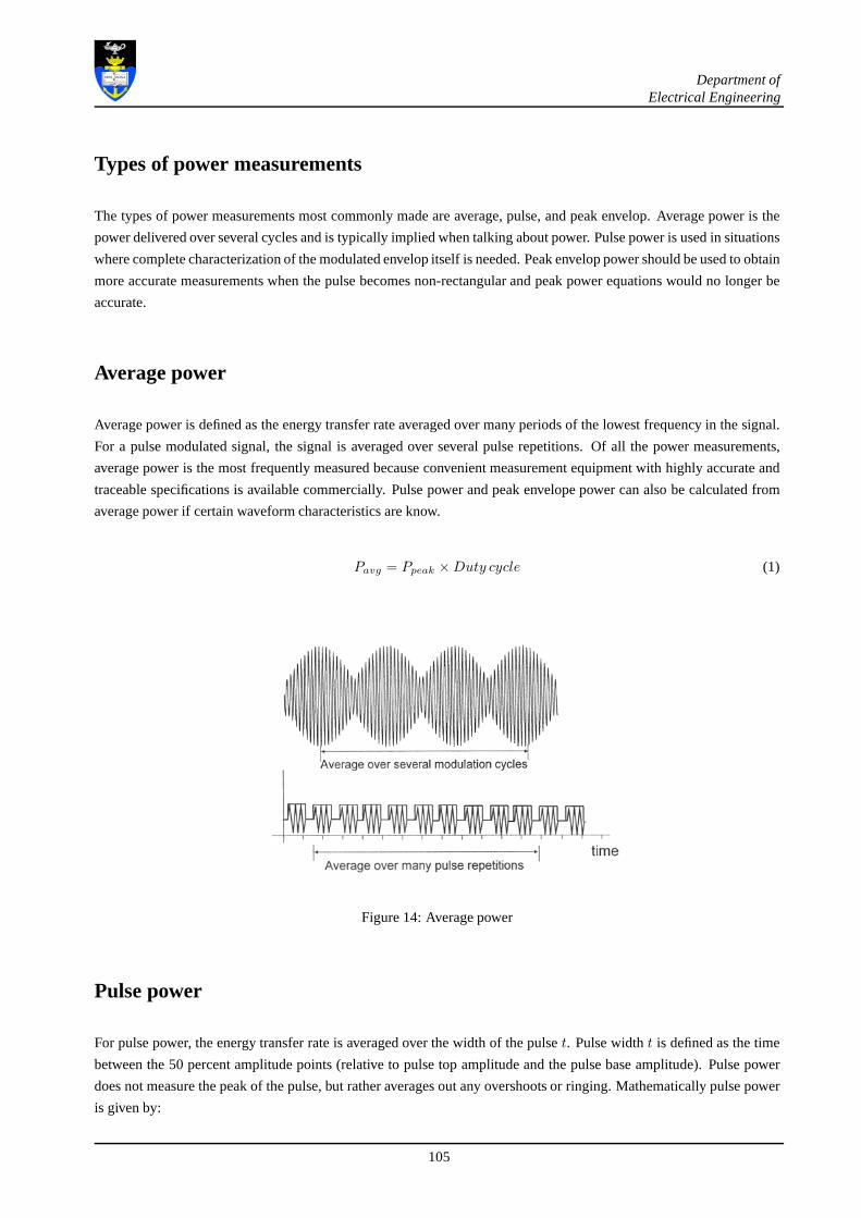
Department ofElectrical Engineering
Types of power measurements
The types of power measurements most commonly made are average, pulse, and peak envelop. Average power is the
power delivered over several cycles and is typically implied when talking about power. Pulse power is used in situations
where complete characterization of the modulated envelop itself is needed. Peak envelop power should be used to obtain
more accurate measurements when the pulse becomes non-rectangular and peak power equations would no longer be
accurate.
Average power
Average power is defined as the energy transfer rate averagedover many periods of the lowest frequency in the signal.
For a pulse modulated signal, the signal is averaged over several pulse repetitions. Of all the power measurements,
average power is the most frequently measured because convenient measurement equipment with highly accurate and
traceable specifications is available commercially. Pulsepower and peak envelope power can also be calculated from
average power if certain waveform characteristics are know.
Pavg = Ppeak × Duty cycle (1)
Figure 14: Average power
Pulse power
For pulse power, the energy transfer rate is averaged over the width of the pulset. Pulse widtht is defined as the time
between the 50 percent amplitude points (relative to pulse top amplitude and the pulse base amplitude). Pulse power
does not measure the peak of the pulse, but rather averages out any overshoots or ringing. Mathematically pulse power
is given by:
105

Department ofElectrical Engineering
PP =1
t
∫e(t) × i(t)dt (2)
Pulse power for a rectangular pulse is also defined by:
PP =Pavg
Duty Cycle(3)
Which is easier to measure at RF using a power meter especially when the duty cycle of the pulse is known.
Note: In finding pulse power we are only interested in the power contained in each pulse. This is why averaging is done
over the pulse width and not over multiple repetitions of thepulse as is done for average power.
Figure 15: Pulse power
Peak Envelope Power
In certain applications, like wireless communications, the pulse shape is rounded to save bandwidth. To narrow the
signal in the frequency domain, the sharp edges present in a square wave must be reduced by widening the signal in the
time domain. Once the pulse deviates substantially from a pure square wave the equations stated earlier are no longer
valid to calculate the power contained in the pulse. Envelope power is used when the pulse power does not give a true
picture of the power in a pulse.
Peak envelope power is a term used for describing the maximumpulse envelope power. Envelope power is measured
by making the averaging time much less than1/f , wheref is the highest frequency component of the modulation
waveform. The averaging time is limited on both ends:
1. It must be small compared to the period of the highest modulation frequency.
2. It must be large enough to be many RF cycles long.
Continuously displaying the envelope power on a peak power analyzer will show the profile of the pulse shape. Peak
106

Department ofElectrical Engineering
envelope power is the maximum value of the envelope power. For rectangular pulses, peak envelope power is equal to
pulse power as defined before and a peak power analyzer would be used to completely characterize the waveform.
Figure 16: Peak envelope power
Summary
• For a CW signal, average, pulse and peak envelope power give the same results.
• Average power is more frequently measured because of easy touse measurement equipment.
• Pulse and peak envelope power can often be calculated from average power.
Making Pulsed RF Measurements
A pulsed RF signal is a train of RF pulses with a constant repetition rate, constant pulse width, shape and amplitude.
A key factor in the measurement of pulse RF signals when usinga spectrum analyzer is the resolution bandwidth used.
When the resolution bandwidth is narrow compared to the pulse repetition frequency (PRF), the display will show the
individual frequency components (actual Fourier representation) making up the pulsed RF signal. This is referred to
as the narrow band mode. A general rule of thumb to obtain a line spectrum on the spectrum analyzer is to set the
resolution bandwidth of the display to less than0.3 × PRF .
When the resolution bandwidth is wide compared to the PRF it is operating in the broad-band mode. The envelope
of the spectrum can be seen traced out by pulse lines, with thedistance between each line equal to the PRF.
107
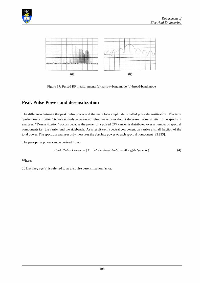
Department ofElectrical Engineering
Figure 17: Pulsed RF measurements (a) narrow-band mode (b) broad-band mode
Peak Pulse Power and desensitization
The difference between the peak pulse power and the main lobeamplitude is called pulse desensitization. The term
“pulse desensitization” is note entirely accurate as pulsed waveforms do not decrease the sensitivity of the spectrum
analyser. “Desensitization” occurs because the power of a pulsed CW carrier is distributed over a number of spectral
components i.e. the carrier and the sidebands. As a result each spectral component on carries a small fraction of the
total power. The spectrum analyser only measures the absolute power of each spectral component [22][23].
The peak pulse power can be derived from:
Peak Pulse Power = (Mainlode Amplitude)− 20 log(duty cycle) (4)
Where:
20 log(duty cycle) is referred to as the pulse desensitization factor.
108

Appendix D
SASAR II board Layout
109
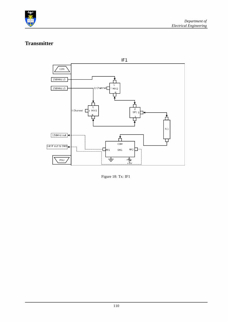
Department ofElectrical Engineering
Transmitter
Figure 18: Tx: IF1
110

Department ofElectrical Engineering
Figure 19: Tx: IF2
111

Department ofElectrical Engineering
Figure 20: Tx: IF2
112

Department ofElectrical Engineering
Receiver
Figure 21: Rx: IF1
113

Department ofElectrical Engineering
Figure 22: Rx: IF2
114
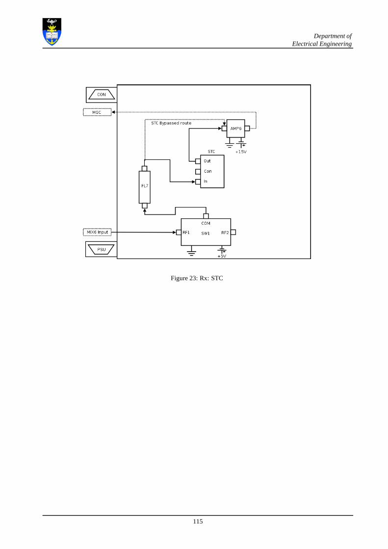
Department ofElectrical Engineering
Figure 23: Rx: STC
115

Department ofElectrical Engineering
Figure 24: Rx: MGC
116
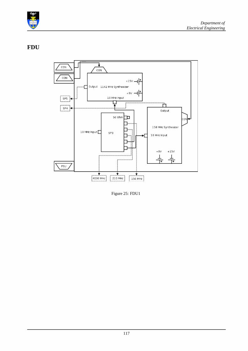
Department ofElectrical Engineering
FDU
Figure 25: FDU1
117

Department ofElectrical Engineering
Figure 26: FDU2
118

Department ofElectrical Engineering
Figure 27: Rx: STC
119

Department ofElectrical Engineering
Figure 28: Rx: STC
120

Department ofElectrical Engineering
Figure 29: SASAR II Front Panel
121

Bibliography
[1] Byron Edde.Radar, Principles, Technology, Applications. Prentice Hall, March 1995.
[2] Coetzer D G.SASAR II FDU Specifications Document. Technical report, University of Cape Town - RRSG 2003.
[3] Coetzer D G.SASAR II Transmitter Specifications Document. Technical report, University of Cape Town - RRSG,
2003.
[4] Coetzer D G.Design and Implementation of a X-Band Transmitter and Frequency Distribution Unit for a Synthetic
Aperture Radar. Masters thesis, University of Cape Town, 2004.
[5] Curlander J C, McDonough R N.Synthetic Aperture Radar Systems and Signal Processing. JohnWiley and Sons,
Jan 1991.
[6] Inggs M R.SASAR II Design Document. Technical report, University of Cape Town - RRSG, 2003.
[7] Inggs M R.SASAR II Subsystem User Requirements. Technical report, University of Cape Town - RRSG, Feb 2003.
[8] Kingsley S, Quegan S.Understanding Radar Systems. McGraw-Hill Book Company, Jan 1992.
[9] Merril Skolnik. Radar Handbook; Second Edition. McGraw-Hill Inc, June 1990.
[10] Merril Skolnik. Introduction to Radar Systems. McGraw-Hill Inc, Jan 2001.
[11] Mohungoo A I.SASAR II Design document of the SAR receiver. Technical report, University of Cape Town -
RRSG, Aug 2003.
[12] Mohungoo A I.An Airborne SAR Receiver Design and Implementation. Masters thesis, University of Cape Town,
2004.
[13] Peebles, Peyton Z. Jr.Radar Principles. John Wiley and Sons, Jan 1998.
[14] Stimson G W.Introduction to Airborne Radar. Jan 1983.
122

Department ofElectrical Engineering
[15] Webster J M.The Development of a Radar Digital Unit for the SASARII Project. Masters thesis, University of
Cape Town, 2004.
[16] Peritek Labs.PM Series user manual.Spectrum Analyzer User Manual, Redwood Oaklands, 2003.
[17] Pozar D M.Microwave and RF Design of Wireless Systems.John Wiley and Sons, 2001.
[18] Stremler F G.Introduction to Communication Systems, 3rd Edition.Addison-Wesley Publishing Company, 1990.
[19] Jerrold Foutz.Switching-mode Power Supply Design Introduction. 2004.
[20] Koeppen P G.Timing Card Specification Document.Technical Report, University of Cape Town - RRSG, 1995.
[21] Da Silveira M D.SASAR II Development Specification.Technical Report, CSIR - Manufacturing & Aeronautical
Systems Technology, 1997.
[22] Marcus Human.Spectrum Analyser Basics.Technical Manual, Agilent Technologies, 2003.
[23] Boyd Shaw.RF Power Measurements.Technical Manual, Agilent Technologies, 2003.
[24] Wilkinson A J.Radar Signal Processing.Course Notes, University of Cape Town, 2002.
[25] Ronald Stirling.Microwave Frequency Synthesis.Prentice Hall, 1987.
[26] P Horowitz. W Hill. The Art of Electronics.Cambirdge University Press, 1995.
[27] Chang K.RF and Microwave Wireless Systems.John Wiley and Sons, 2000.
[28] Sen P C.Principles of Electronic Machines and Power Electronics.John Wiley and Sons, 2000.
[29] Nathasan F E.Radar Design Principles.McGraw-Hill Book Company, 1969.
123