Embed Size (px)
Citation preview

Int. J. Surface Science and Engineering, Vol. 5, Nos. 2/3, 2011 193
Copyright © 2011 Inderscience Enterprises Ltd.
Nanomechanical study of amorphous and polycrystalline ALD HfO2 thin films
K. Tapily* Department of Electrical Engineering, Old Dominion University, Norfolk, Virginia 23529, USA and Applied Research Center, Newport News, Virginia, 23606, USA E-mail: [email protected] *Corresponding author
J.E. Jakes Performance Enhanced Biopolymers, USDA Forest Products Laboratory, Madison, Wisconsin, 53726, USA and Department of Materials Science and Engineering, University of Wisconsin-Madison, Madison, Wisconsin 53706, USA E-mail: [email protected]
D. Gu and H. Baumgart Department of Electrical Engineering, Old Dominion University, Norfolk, Virginia 23529, USA and Applied Research Center, Newport News, Virginia, 23606, USA E-mail: [email protected] E-mail: [email protected]
A.A. Elmustafa Applied Research Center, Newport News, Virginia, 23606, USA and Department of Mechanical Engineering, Old Dominion University, Norfolk, Virginia 23529, USA E-mail: [email protected]
194 K. Tapily et al.
Abstract: Thin films of hafnium oxide (HfO2) were deposited by atomic layer deposition (ALD). The structural properties of the deposited films were characterised by transmission electron microscopy (TEM) and X-ray diffraction (XRD). We investigated the effect of phase transformations induced by thermal treatments on the mechanical properties of ALD HfO2 using nanoindentation. The elastic modulus of the amorphous low temperature deposited ALD HfO2 films was measured to be 370 ± 20 GPa. Subsequent to crystallisation by annealing in a rapid thermal annealing (RTA) chamber, the elastic modulus dropped to 240 ± 20 GPa. Similarly, the Meyer hardness decreased from a value of 18 ± 1 GPa for amorphous HfO2 to 15 ± 1 GPa following the transition temperature from amorphous to polycrystalline HfO2.
Keywords: atomic layer deposition; ALD; nanoindentation; high-k dielectrics; modulus; hardness; hafnium oxide; HfO2.
Reference to this paper should be made as follows: Tapily, K., Jakes, J.E., Gu, D., Baumgart, H. and Elmustafa, A.A. (2011) ‘Nanomechanical study of amorphous and polycrystalline ALD HfO2 thin films’, Int. J. Surface Science and Engineering, Vol. 5, Nos. 2/3, pp.193–204.
Biographical notes: Kandabara Tapily received his PhD in Electrical and Computer Engineering from Old Dominion University. He is currently a Research Assistant at the ODU Applied Research Center, Newport News VA. His research focuses on atomic layer deposition (ALD) of various thin films and their characterisation. He also studies ALD of semiconductor ZnO for optoelectronics applications.
Joseph E. Jakes received his PhD of the Materials Science Program at the University of Wisconsin-Madison in 2010. He is currently a Research Materials Engineer in Performance Enhanced Biopolymers Group at the USDA Forest Products Laboratory and a Visiting Scientist at the Materials Science and Engineering, University of Wisconsin-Madison. His research interests include investigating subcellular structure-property relationships in wood and developing advanced nanoindentation techniques.
Diefeng Gu received his PhD in Materials Science from Arizona State University in 2006. Currently, he works as a Research Scientist in the Department of Electrical and Computer Engineering and the Applied Research Center at Old Dominion University. His research interests include atomic layer deposition (ALD) of various thin films and characterisation; high-k dielectrics for microelectronics devices; semiconductor oxide films for organic solar cells, ALD of ZnO thin film coating for phosphors and nanotubes for detector and sensor applications.
Helmut Baumgart received his PhD in Semiconductor Physics from the University of Stuttgart and Max-Planck Institute of Solid State Research, Stuttgart, Germany. His research interests are: nanotechnology; microelectronics fabrication; high-k dielectrics for advanced gate stack engineering; atomic layer deposition (ALD) technology of electronic thin film materials; semiconductor device processing; thin film growth; ALD of ZnO for detector and sensor applications.
Abdelmageed A. Elmustafa received his PhD in Materials Science and Engineering from the University of Wisconsin-Madison in 2000. Currently, he is an Assistant Professor in the Department of Mechanical Engineering and the Applied Research Center at Old Dominion University, and a Visiting Research Professor in the Department of Mechanical and Aerospace Engineering at

Nanomechanical study of amorphous and polycrystalline ALD HfO2 thin films 195
Princeton University. He has extensive experience in the nanoscale mechanical behaviour of materials and nanotechnology with research interests in nanoindentation; dislocation and strain gradient plasticity; thin films; modelling and simulation; nanopositioners. He has served as a Technical Reviewer for the National Science Foundation and as a Reviewer for 20 refereed journals.
1 Introduction
As the device feature size gets smaller and smaller, it is increasingly difficult to reduce the gate leakage and the tunnelling current in the SiO2 and SiON layer for the state-of-the-art and future nanotechnology nodes. For this reason, novel high-k dielectric materials are attracting a lot of attention for microelectronics device fabrication. Hf-based dielectrics have emerged as one of the leading candidates to replace SiO2 and SiON as gate dielectric in the 45 nm technology node and beyond for CMOS devices because of their high dielectric constant and thermal stability on silicon, as discussed by Wilk et al. (2008). Although detailed studies exist on the electrical characterisation of HfO2, its mechanical properties still need to be investigated. The most widely used techniques to deposit HfO2 films are metal organic chemical vapour deposition (MOCVD) as shown by Dubourdieu et al. (2005), Jones et al. (2005) and Triyoso et al. (2005), pulsed laser deposition (PLD) as shown by Ikeda et al. (2002), and atomic layer deposition (ALD) as shown by Delabie et al. (2002). ALD offers uniform film thickness, better control over deposition parameters and superior film conformity over complex surface topographies (Ritala and Leskela, 2002). At high temperature growth, HfO2 undergoes a phase transformation. Neumayer and Cartier (2001) have shown that HfO2 crystallises into monoclinic polycrystalline films around 300–500°C. The phase change of HfO2 was also confirmed by Gusev et al. (2006). This phase transformation increases the surface roughness and the grain boundary-induced gate leakage current which is not desirable in CMOS devices as discussed by Zhu et al. (2002). However, Hausmann and Gordon (2003) showed that by initially depositing amorphous HfO2 films at low temperatures, smoother film surface and interface morphologies are obtained and the phase change to polycrystalline HfO2 is delayed to later stages in the CMOS processing. Integrating high-k HfO2 as gate insulator replacement into state-of-the-art CMOS processes is subjecting the HfO2 films to multiple thermal cycles. Although ALD HfO2 is initially deposited in the amorphous phase at low temperatures, these multiple thermal cycles inherent to CMOS device processing cause a phase change of the HfO2 film from amorphous to polycrystalline. Little is known about the impact of these phase changes on the nanomechanical properties of ALD HfO2. In this study, we conducted nanoindentation testing to investigate the impact of the different phase changes of HfO2 on the mechanical properties.
Nanoindentation is often used to assess the hardness and elastic modulus of thin films (e.g., Stone et al., 1991; Saha and Nix, 2002). In nanoindentation, a carefully shaped indenter is used to probe the properties of a material by applying a well-defined loading protocol while continuously measuring changes in depth. A typical experiment consists of a loading segment, followed by hold at a prescribed maximum load to allow

196 K. Tapily et al.
time-dependent creep processes to dissipate, and finally, an unloading segment. The Meyer hardness, H, assesses plastic properties and is defined by
PHA
= (1)
where P is the load immediately prior to unloading and A is the area of the indent. The P – depth (h) unloading trace is fit to a power law and the initial unloading stiffness (dP/dh) assessed following the usual Oliver-Pharr approach (Oliver and Pharr, 1992). The ‘effective’ modulus of contact is then defined as
1eff
dPEdhA
= (2)
For indentation against a homogeneous, isotropic, elastic half-space Eeff is related to material properties by
2 21 11 1 s d
eff s dE E Eν ν
β⎛ ⎞− −
= +⎜ ⎟⎜ ⎟⎝ ⎠
(3)
where Es and Ed are Young’s moduli and νs and νd are Poisson’s ratios of specimen and indenter, respectively. β is a numerical factor which is often taken as 2 / .π In previous studies it was found that β = 1.23 fits data better and so we will use this value (Jakes et al., 2008). If the half-space is layered, then the first term in parentheses in equation (3) must be replaced by 1/Er, where Er depends upon the size of the indent in relation to the layer thickness (Stone, 1998).
The unloading cycle in nanoindentation using the standard Oliver-Pharr method is purely elastic. Under certain circumstance, it is viscoelastic. To correct for this effect, a correction factor is used to reduce the effect of creep as discussed by Ngan et al. (2005). Recently, Elmustafa and Stone (2007) have shown that the strain rate sensitivity of the hardness and that of the flow stress differs significantly for materials with high hardness modulus ratio in indentation creep experiments. Stone and Yoder (2004) concluded that the hardness measurements will yield the same results for indentation load relaxation, rate change, or indentation creep experiments. It can therefore be concluded that the effect of creep is not significant for these materials (Elmustafa and Stone, 2007). In addition, the measured creep factor of Feng and Ngan (2002) for our data is always below 0.3%. Therefore, creep does not influence the unloading slope.
When ALD HfO2 is integrated into a full CMOS process to replace conventional field-effect transistor (FET) gate insulators, it will always end up with the polycrystalline phase, because the thermal budget rises above the transition temperature. That phase change of HfO2 affects a number of important parameters in device processing. In this study, we deposit HfO2 films at two different temperatures and thicknesses using ALD, and then anneal the films at high temperatures. The structural properties of the films before and after annealing are characterised by transmission electron microscopy (TEM), and X-ray diffraction (XRD). We find annealing causes the initial amorphous structure to transition to a polycrystalline structure. Using nanoindentation, we find the hardness and elastic modulus of the films decrease after annealing.

Nanomechanical study of amorphous and polycrystalline ALD HfO2 thin films 197
2 Experimental details
HfO2 films were deposited by ALD on 4-inch p-type Si (100) wafers. The Si substrate wafers were cleaned with a diluted 2% HF solution at room temperature to remove the native oxide and then dried in N2. Subsequently, we deposited HfO2 films using the Cambridge Nanotech Savannah 100 ALD reactor. The deposition of HfO2 consisted of consecutive pulses of tetrakisdimethylamidohafnium IV as the precursor for hafnium and water vapour as the oxygen source. The hafnium precursor was heated at a temperature of 75°C. The precursors were directly delivered to the reaction chamber through stainless tubes filled with a carrier gas N2. The deposition temperatures were selected in order to deposit amorphous films. 600 cycles were used to deposit two-samples of HfO2 films each of thickness of 62 nm at 185°C and 200°C, respectively. The water vapour precursor was pulsed for 25 ms, whereas, the hafnium precursor was pulsed for 1 s. The thickness was doubled to 120 nm to investigate the effects of thickness on the mechanical properties. 1,200 cycles were used to deposit two-samples of HfO2 films each of thickness of 120 nm at 185°C and 200°C respectively. The ALD chamber pressure was kept at 2.8 ×10 –1 Torr for all depositions. After the deposition, a portion of the wafers was subdivided by cleaving and annealed at 400°C and 600°C in nitrogen using the Solaris 150 rapid thermal annealing (RTA) system from SSI – surface science integration. A summary of the samples preparation is given in Table 1. Table 1 Summary of the sample as-deposited and annealed
Specimen Thickness (nm)**
Deposition temperature (°C)
Annealing temperature (°C)
Annealing time (min)
a-HfO* 120 185 Not annealed Not annealed poly-HfO 1 120 185 600 3 poly-HfO 2 62 200 400 1 poly-HfO 3 62 200 600 3
Notes: *a-HfO stands for amorphous HfO2. **The film thicknesses were measured using a spectroscopic ellipsometer (VASE, Woollam).
The cross-sectional analysis was done by Jeol JEM 2100F high resolution transmission electron microscope (HRTEM). A Rigaku Miniflex was used to study the crystal growth of the as-deposited and annealed sample by XRD. A Hysitron (Minneapolis, Minnesota, USA) TriboIndenter equipped with a diamond Berkovich tip and operated in open-loop control was used in this work. The machine compliance was evaluated using data from a series of indents with different loads placed in the centre of a fused silica standard and the SYS correlation (Stone et al., 1991; Jakes et al., 2008). Figure 1(a) shows the basic load function for the experiments on the HfO2 films. Series of 20 indents were placed on each film beginning with a maximum load of 0.01 mN. Each successive indent’s maximum load increased by 44% and the final indent had a 10.2 mN maximum load. Figure 1(b) shows load-depth traces from one series of indents. A Quesant (Agoura Hills, California, USA) atomic force microscope (AFM) incorporated in the TriboIndenter was used to image all residual indents. The AFM was operated in contact mode and calibrated using an Advanced Surface Microscopy Inc. (http://www.asmicro.com) calibration standard with a pitch of 292 ± 0.5 nm. Successive scans and calibration routines reveal the reproducibility of the AFM calibration to be ±1%. ImageJ (http://rsb.info.nih.gov/ij/)

198 K. Tapily et al.
image analysis software was used to manually measure the areas from 4 μm field-of-view images following the procedure outlined by Jakes et al. (2008). The measured areas were used to calculate the effective modulus [equation (2)] and Meyer hardness [equation (1)]. Only indents with well defined residual indent impressions that could be observed in the AFM images (Figure 2) were included in the assessment of hardness and elastic modulus. The nanoindentation experiments were carried out at room temperature.
Figure 1 (a) Load function used in this study, which consisted of a 2 s loading, 5 s hold at maximum load, 1 s unload to 25% of the maximum load, 30 s hold at 25% maximum load, 1 s final unload, and a 2 s hold at zero load*, (b) load-depth traces for 20 indents performed on a 62 nm HfO2 film deposited at 200°C and annealed at 600°C in nitrogen in 3 min (poly-HfO 3)
(a) (b)
Notes: *The 30 s hold was used to correct the load-depth trace for thermal drift and the 2 s hold was used to assure the load was properly zeroed. The maximum loads ranged from 0.01–10.2 mN.
Figure 2 AFM micrographs of a 10.2 mN indent and 0.13 mN indent (insert) placed on a 62 nm HfO2 film deposited at 200°C and annealed at 600°C in nitrogen in 3 min (poly-HfO 3)
Nanomechanical study of amorphous and polycrystalline ALD HfO2 thin films 199
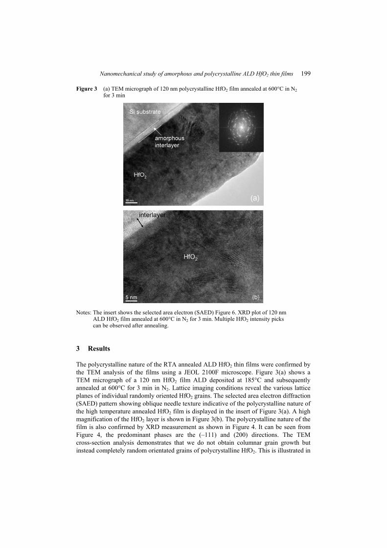
Figure 3 (a) TEM micrograph of 120 nm polycrystalline HfO2 film annealed at 600°C in N2 for 3 min
Notes: The insert shows the selected area electron (SAED) Figure 6. XRD plot of 120 nm ALD HfO2 film annealed at 600°C in N2 for 3 min. Multiple HfO2 intensity picks can be observed after annealing.
3 Results
The polycrystalline nature of the RTA annealed ALD HfO2 thin films were confirmed by the TEM analysis of the films using a JEOL 2100F microscope. Figure 3(a) shows a TEM micrograph of a 120 nm HfO2 film ALD deposited at 185°C and subsequently annealed at 600°C for 3 min in N2. Lattice imaging conditions reveal the various lattice planes of individual randomly oriented HfO2 grains. The selected area electron diffraction (SAED) pattern showing oblique needle texture indicative of the polycrystalline nature of the high temperature annealed HfO2 film is displayed in the insert of Figure 3(a). A high magnification of the HfO2 layer is shown in Figure 3(b). The polycrystalline nature of the film is also confirmed by XRD measurement as shown in Figure 4. It can be seen from Figure 4, the predominant phases are the (–111) and (200) directions. The TEM cross-section analysis demonstrates that we do not obtain columnar grain growth but instead completely random orientated grains of polycrystalline HfO2. This is illustrated in

200 K. Tapily et al.
Figure 3(b). An interlayer (IL) growth of hafnium silicate was observed on the polycrystalline HfO2 films provided in Figures 3(a) and 3(b). The IL growth is due to the thermally activated diffusion of hafnium and oxygen into the silicon substrate, where these constituents react with Si forming a layer of hafnium silicate. A 4 nm thick amorphous IL of hafnium silicate is observed in the polycrystalline films.
Figure 4 XRD plot of 120 nm ALD HfO2 film annealed at 600°C in N2 for 3 min
Note: Multiple HfO2 intensity picks can be observed after annealing.
A cross-sectional TEM analysis was also performed on the amorphous ALD films. Figure 5(a) shows the TEM micrograph of a 120 nm HfO2 deposited at 185°C before high magnification. Figure 5(b) displays the as-deposited 120 nm HfO2 and proves that this film is fully amorphous by showing the SAED with the typical broad amorphous ring diffraction pattern with no speckle in the insert. It is noteworthy that no IL growth was visible in amorphous films shown in Figures 5(a) and 5(b).
The elastic modulus (Es) of the films are estimated by comparing experimental effective modulus (Eeff) with Eeff calculated from simulations of thin films with different Es. The simulations are based on Stone’s model of elastic rebound between an indenter and layered specimen (Stone, 1998). In this model, the effects of the silicon substrate underneath the HfO2 film and the diamond indenter are taken into account. The elastic properties of silicon used in the simulation were 161 GPa for Es and 0.227 for Poisson’s ratio (νs). The νs for the HfO2 film was assumed to be 0.3. Data are normalised to the film thickness, allowing films of varying thicknesses to be directly compared to the same simulations. It is notable that the only fitting parameter in Stone’s model is the nanoindentation correction factor β which is dependent on the indenter geometry, tip bluntness and Poisson’s ratio of the material being indented. The correction factor β was determined independently for the diamond Berkovich indenter used in this study to equal 1.23 (Jakes et al., 2008).

Nanomechanical study of amorphous and polycrystalline ALD HfO2 thin films 201
Figure 5 (a) TEM micrograph of 120 nm ALD HfO2 film deposited at 185°C*, (b) TEM micrograph of 120 nm ALD HfO2 film deposited at 185°C and its SAED pattern in the insert
Notes: *The micrograph shows the total thickness of HfO2 on top of the Si substrate. The diffuse ring texture of the electron diffraction pattern proves that the as-deposited HfO2 is in its amorphous phase.
Comparing the experimental data points to the simulated curves, it is evident that Es for the as-deposited amorphous HfO2 film is approximately 370 ± 20 GPa. It is also observed that the Es decreases in the films after annealing. For example, the Es of films annealed for 3 min at 600ºC is about 240 ± 20 GPa. The Meyer hardness (H) is plotted versus the normalised square root of contact area in Figure 6(b). The hardness was found to be 18 ± 1 GPa for the as-deposited amorphous HfO2 film and decreased to about 15 ± 1 GPa after annealing at 600°C. Our measurements clearly demonstrate that the initially amorphous ALD HfO2 film behaves differently compared to its final polycrystalline phase. After high temperature annealing, the H and Es drop significantly from the as-deposited amorphous films to the annealed recrystallised films.

202 K. Tapily et al.
Figure 6 (a) Effective modulus vs. square root of area normalised with the film thickness*, (b) hardness vs. square root of area normalised with the thickness
Notes: The symbols represent experimental data and the dashed lines are the calculated results of Stone’s model for films with different Es. Eeff = effective modulus, A= contact area, h = film thickness, αHfO = aHfO2 (amorphous HfO2). H = hardness, A= contact area, h= film thickness, αHfO = aHfO2 (amorphous HfO2).
4 Discussion
Our nanoindentation analysis demonstrates that the initial low temperature ALD deposited HfO2 in its amorphous state is harder and stiffer than the polycrystalline form of HfO2 obtained later by annealing past the transition temperature for crystallisation around 600°C. This result can be understood on the basis of the specific micro structural properties of the two different phases of HfO2, which were investigated. Plastic deformation in crystalline solids occurs via nucleation and multiplication of crystal lattice defects such as dislocations and their interaction with low-angle grain boundaries. Above the transition temperature for crystallisation ALD HfO2 films turned into fine grained polycrystalline material with random grain orientation, which is demonstrated in our high resolution X-TEM micrograph of Figures 3(a) and 3(b). In addition to the large number of grain boundaries each individual grain of the randomly nucleated polycrystalline HfO2 film typically contains dislocations and stacking faults. Therefore, there is no shortage of lattice defects in our recrystallised HfO2 films which tend to facilitate the plastic deformation during the loading cycle of the nanoindentation process. This defect-aided plastic deformation can explain the lowering of the hardness values for recrystallised HfO2 films. By definition, the initial amorphous phase of low temperature ALD deposited HfO2 does not contain any extended crystal lattice defects which result in making the material harder to deform. A similar argument can be made to explain the difference in the elastic modulus between the amorphous and the crystalline phase of HfO2.
When ALD HfO2 is integrated into a full CMOS process to replace conventional FET gate insulators, it will always end up with the polycrystalline phase, because the thermal budget rises above the transition temperature. That phase change of HfO2 affects a number of important parameters in device processing. The lowering of the hardness and elastic modulus is beneficial, because it can help reduce interfacial stress build-up in the back-end (BEOL) of the integrated CMOS and thus mitigate process-induced defect

Nanomechanical study of amorphous and polycrystalline ALD HfO2 thin films 203
nucleation in CMOS devices. However, the phase change to polycrystalline material is accompanied by spontaneous grain growth. Furthermore, as a less desirable consequence, the grain boundaries tend to act as a preferred leakage path and are associated with higher leakage currents compared to the amorphous phase.
5 Conclusions
HfO2 has drawn attention as a promising high-k material candidate to replace SiO2 and SiON as MOSFET gate insulator beyond the 45 nm technology node. However, ALD HfO2 films undergo phase changes from initially amorphous to polycrystalline structure as a function of thermal annealing temperature during standard CMOS device processing. We have deposited ALD HfO2 at low temperature and measured the mechanical properties of the various phase changes of HfO2 following various thermal annealing cycles. The modulus was found to decrease from 370 ± 20 GPa to 240 ± 20 GPa as the HfO2 films transition from amorphous to polycrystalline structure past the phase change transition temperature of 600°C. Similarly, the hardness measurements reveal a high value of 18 ± 1 GPa for amorphous HfO2 films and a decrease to 15 ± 1 GPa following the transition temperature to polycrystalline HfO2 films. The high temperature phase change to polycrystalline HfO2 causes an increased HfO2 interface roughness due to spontaneous grain nucleation and grain growth and a significant drop of HfO2 hardness and elastic modulus, which has implications on leakage behaviour, and affects the process integration of this novel high-k material into CMOS processes.
References Delabie, A., Caymax, M., Maes, J.W., Bajolet, P., Brijs, B., Cartier, E., Conard, T., De Gendt, S.,
Richard, O., Vandervorst, W., Zhao, C., Green, M., Tsai, W. and Heyns, M.M. (2002) ‘ALD HfO2 surface preparation study’, in Proc. Mater. Res. Soc. Symp., Vol. 745, pp.179–184.
Dubourdieu, C., Roussel, H., Jimenez, C., Audier, M., Senateur, J.P., Lhostis, S., Auvray, L., Ducroquet, F.O., Sullivan, B.J., Hurley, P.K., Rushworth, S. and Hubert-Pfalzgraf, L. (2005) ‘Pulsed liquid-injection MOCVD of high-K oxides for advanced semiconductor technologies’, Material Science Engineering B, Vol. 118, Nos. 1–3, pp.105–111.
Elmustafa, A.A. and Stone, D.S. (2007) ‘Strain rate sensitivity in nanoindentation creep of hard materials’, Journal of Material Research, Vol. 22, No. 10, pp.2912–2916.
Feng, G. and Ngan, A.H.W. (2002) ‘Effects of creep and thermal drift on modulus measurement using depth-sensing indentation’, Journal of Material Research, Vol. 17, pp.660–668.
Gusev, E.P., Narayanan, V. and Frank, M.M. (2006) ‘Advanced high-κ dielectric stacks with polySi and metal gates: recent progress and current challenges’, IBM Journal of Research and Development, Vol. 50, Nos. 4–5, pp.387–410.
Hausmann, D.M. and Gordon, R.G. (2003) ‘Surface morphology and crystallinity control in the atomic layer deposition (ALD) of hafnium and zirconium oxide thin films’, Journal of Crystal Growth, Vol. 249, pp.251–261.
Ikeda, H., Goto, S., Honda, K., Sakashita, M., Sakai, A., Zaima, S. and Yasuda, Y. (2002) ‘Structural and electrical characteristics of HfO2 films fabricated by pulsed laser deposition’, Japanese Journal of Applied Physics, Vol. 41, pp.2476–2479.
Jakes, J.E., Frihart, C.R., Beecher, J.F., Moon, R.J. and Stone, D.S. (2008) ‘Experimental method to account for structural compliance in nanoindentation measurements’, Journal of Materials Research, Vol. 23, No. 4, pp.1113–1127.

204 K. Tapily et al.
Jones, A.C., Aspinall, H.C., Chalker, P.R., Potter, R.J., Kukli, K., Rahtu, A., Ritala, M. and Leskela, M. (2005) ‘Recent developments in the MOCVD and ALD of rare earth oxides and silicates’, Material Science Engineering B, Vol. 118, Nos. 1–3, pp.97–104.
Neumayer, D.A. and Cartier, E. (2001) ‘Materials characterization of ZrO2-SiO2 and HfO2-SiO2 binary oxides deposited by chemical solution deposition’, Journal of Applied Physics, Vol. 90, No. 4, pp.1801–1808.
Ngan, A.H.W., Wang, H.T., Tang, B. and Sze, K.Y. (2005) ‘Correcting power-law viscoelastic effects in elastic modulus measurement using depth-sensing indentation’, International Journal of Solids and Structures, Vol. 42, pp.1831–1846.
Oliver, W.C. and Pharr, G.M. (1992) ‘An improved technique for determining hardness and elastic modulus using load and displacement sensing indentation experiments’, Journal Materials Research, Vol. 7, No. 6, pp.1564–1583.
Ritala, M. and Leskela, M. (2002) ‘ Atomic layer deposition’, in Nalwa, H.S. (Ed.): Handbook of Thin Film Materials, Vol. 1, pp.103–158, Academic Press, San Diego, CA.
Saha, R. and Nix, W.D. (2002) ‘Effects of the substrate on the determination of thin film mechanical properties by nanoindentation’, Acta Materialia, Vol. 50, No. 1, pp.23–38.
Stone, D.S. (1998) ‘Elastic rebound between an indenter and a layered specimen I: model’, Journal Material Research, Vol. 13, No. 3, pp.3207–3213.
Stone, D.S., Yoder, K.B. and Sproul, W.D. (1991) ‘Hardness and elastic modulus of TiN based on continuous indentation technique and new correlation’, Journal of Vacuum Science and Technology, Vol. 9, No. 4, pp.2543–2547.
Triyoso, D.H., Ramon, M., Hegde, R.I., Roan, D., Garcia, R., Baker, J., Wang, X.D., Fejes, P., White, B.E. and Tobina, P.J. (2005) ‘Physical and electrical characteristics of HfO2 gate dielectrics deposited by ALD and MOCVD’, Journal of Electrochemical Society, Vol. 152, No. 3, pp.G203–G209.
Wilk, G.D., Wallace, R.M. and Anthony, J.M. (2000) ‘Hafnium and zirconium silicates for advanced gate dielectrics’, Journal of Applied Physics, Vol. 87, No. 1, pp.484–492.
Zhu, W.J., Tamagawa, T., Gibson, M., Furukawa, T. and Ma, T.P. (2002) ‘Effect of Al inclusion in HfO2 on the physical and electrical properties of the dielectrics’, IEEE Electron Device Letters, Vol. 23, No. 11, pp.649–651.