Embed Size (px)
Citation preview
Testing NEXYS 3 Board
Instructions on how to test Digilent NEXYS 3 Board
Testing NEXYS 3 Board
1. ADEPT installation on your PC:
In order to test the NEXYS 3, you need to install ADEPT software on your PC. If you are
working with Lab computers, ADEPT is pre-installed.
In case you want to install the ADEPT software at home, go to link given below.
http://www.digilentinc.com/Products/Detail.cfm?NavPath=2,66,828&Prod=ADEPT2
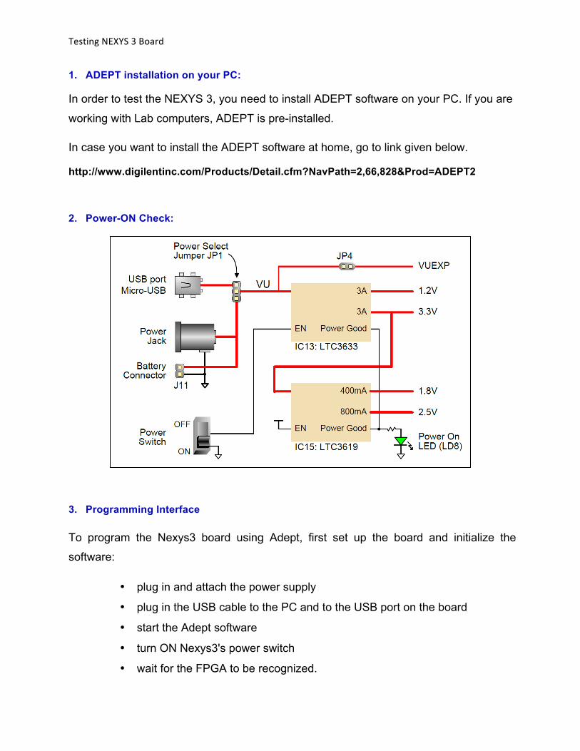
2. Power-ON Check:
3. Programming Interface
To program the Nexys3 board using Adept, first set up the board and initialize the
software:
• plug in and attach the power supply
• plug in the USB cable to the PC and to the USB port on the board
• start the Adept software
• turn ON Nexys3's power switch
• wait for the FPGA to be recognized.
Testing NEXYS 3 Board
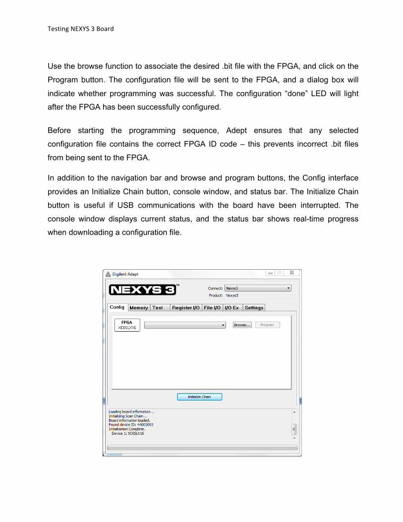
Use the browse function to associate the desired .bit file with the FPGA, and click on the
Program button. The configuration file will be sent to the FPGA, and a dialog box will
indicate whether programming was successful. The configuration “done” LED will light
after the FPGA has been successfully configured.
Before starting the programming sequence, Adept ensures that any selected
configuration file contains the correct FPGA ID code – this prevents incorrect .bit files
from being sent to the FPGA.
In addition to the navigation bar and browse and program buttons, the Config interface
provides an Initialize Chain button, console window, and status bar. The Initialize Chain
button is useful if USB communications with the board have been interrupted. The
console window displays current status, and the status bar shows real-time progress
when downloading a configuration file.
Testing NEXYS 3 Board
4. Memory Interface
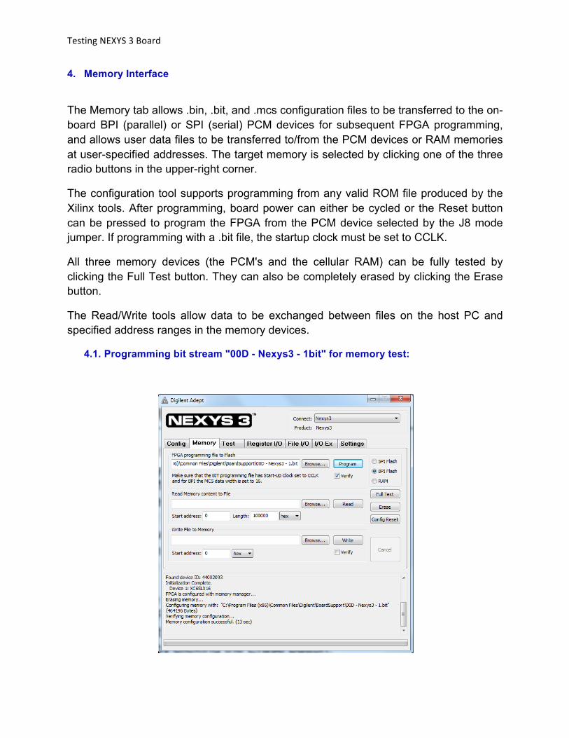
The Memory tab allows .bin, .bit, and .mcs configuration files to be transferred to the on-board BPI (parallel) or SPI (serial) PCM devices for subsequent FPGA programming, and allows user data files to be transferred to/from the PCM devices or RAM memories at user-specified addresses. The target memory is selected by clicking one of the three radio buttons in the upper-right corner.
The configuration tool supports programming from any valid ROM file produced by the Xilinx tools. After programming, board power can either be cycled or the Reset button can be pressed to program the FPGA from the PCM device selected by the J8 mode jumper. If programming with a .bit file, the startup clock must be set to CCLK.
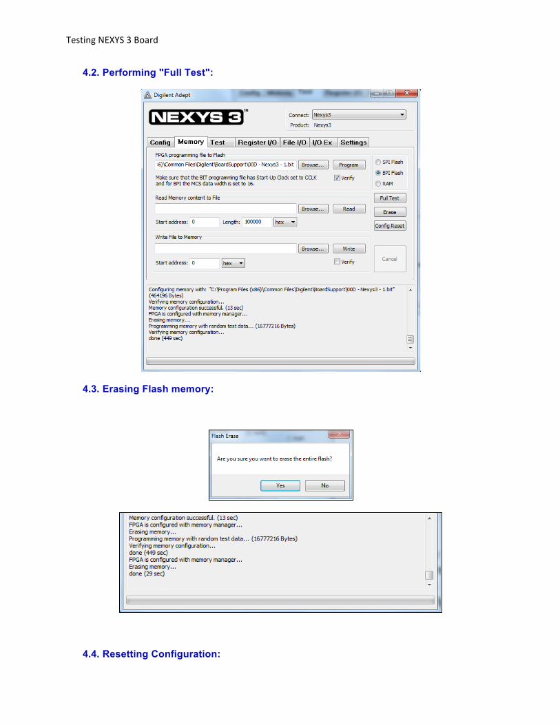
All three memory devices (the PCM's and the cellular RAM) can be fully tested by clicking the Full Test button. They can also be completely erased by clicking the Erase button.
The Read/Write tools allow data to be exchanged between files on the host PC and specified address ranges in the memory devices.
4.1. Programming bit stream "00D - Nexys3 - 1bit" for memory test:
Testing NEXYS 3 Board
4.2. Performing "Full Test":
4.3. Erasing Flash memory:
4.4. Resetting Configuration:
Testing NEXYS 3 Board
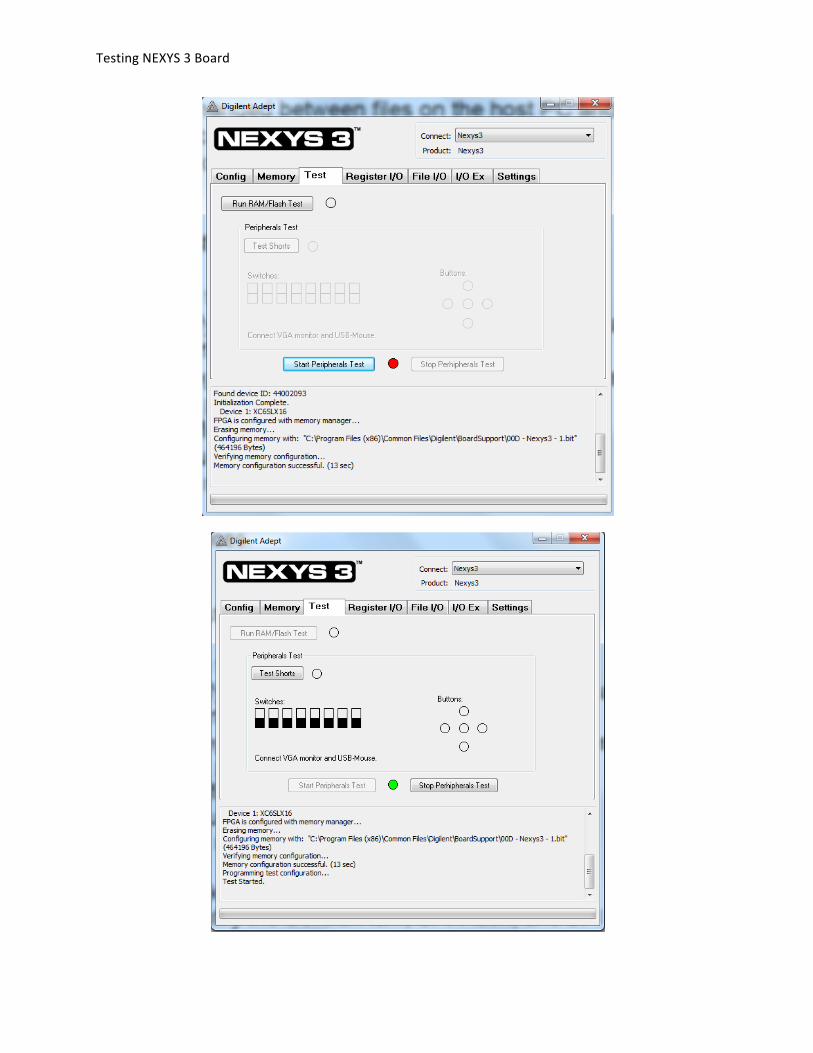
5. Test Interface
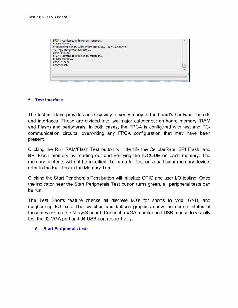
The test interface provides an easy way to verify many of the board's hardware circuits and interfaces. These are divided into two major categories: on-board memory (RAM and Flash) and peripherals. In both cases, the FPGA is configured with test and PC-communication circuits, overwriting any FPGA configuration that may have been present.
Clicking the Run RAM/Flash Test button will identify the CellularRam, SPI Flash, and BPI Flash memory by reading out and verifying the IDCODE on each memory. The memory contents will not be modified. To run a full test on a particular memory device, refer to the Full Test in the Memory Tab.
Clicking the Start Peripherals Test button will initialize GPIO and user I/O testing. Once the indicator near the Start Peripherals Test button turns green, all peripheral tests can be run.
The Test Shorts feature checks all discrete I/O’s for shorts to Vdd, GND, and neighboring I/O pins. The switches and buttons graphics show the current states of those devices on the Nexys3 board. Connect a VGA monitor and USB mouse to visually test the J2 VGA port and J4 USB port respectively.
5.1. Start Peripherals test:
Testing NEXYS 3 Board
Testing NEXYS 3 Board
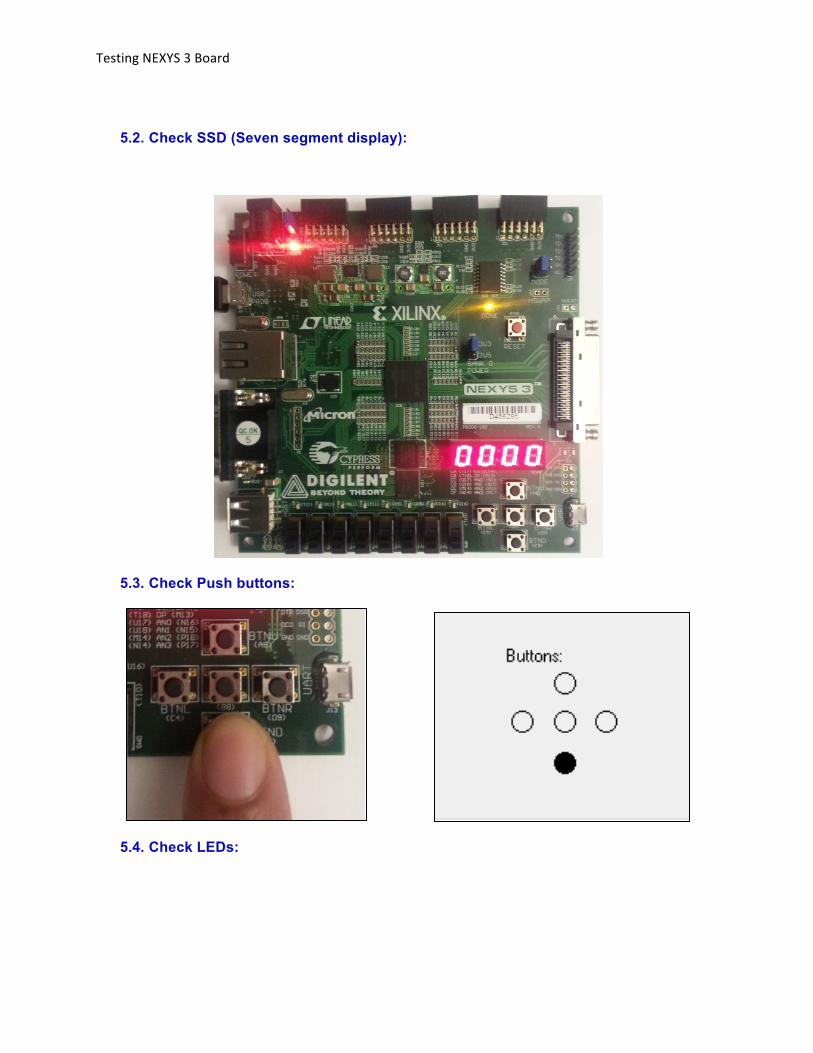
5.2. Check SSD (Seven segment display):
5.3. Check Push buttons:
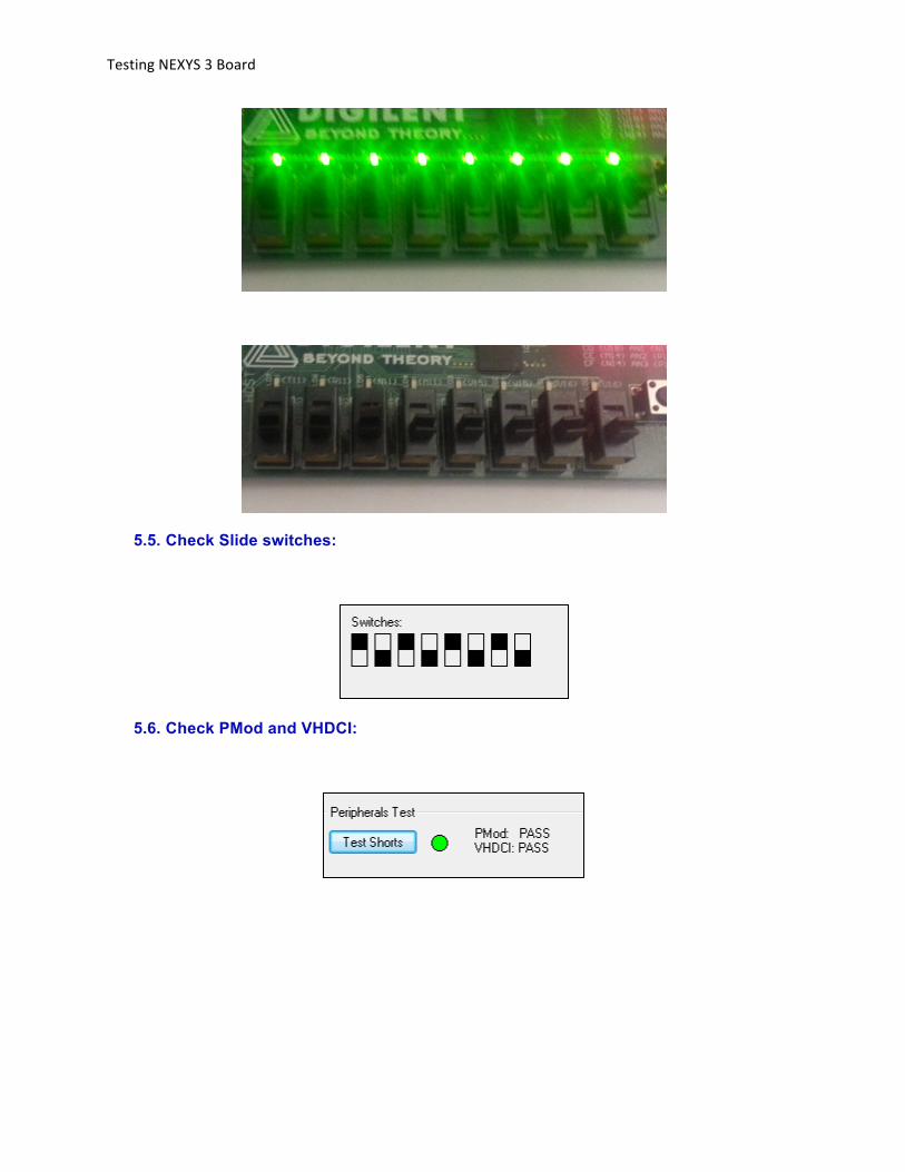
5.4. Check LEDs:
Testing NEXYS 3 Board
5.5. Check Slide switches:
5.6. Check PMod and VHDCI:
Testing NEXYS 3 Board
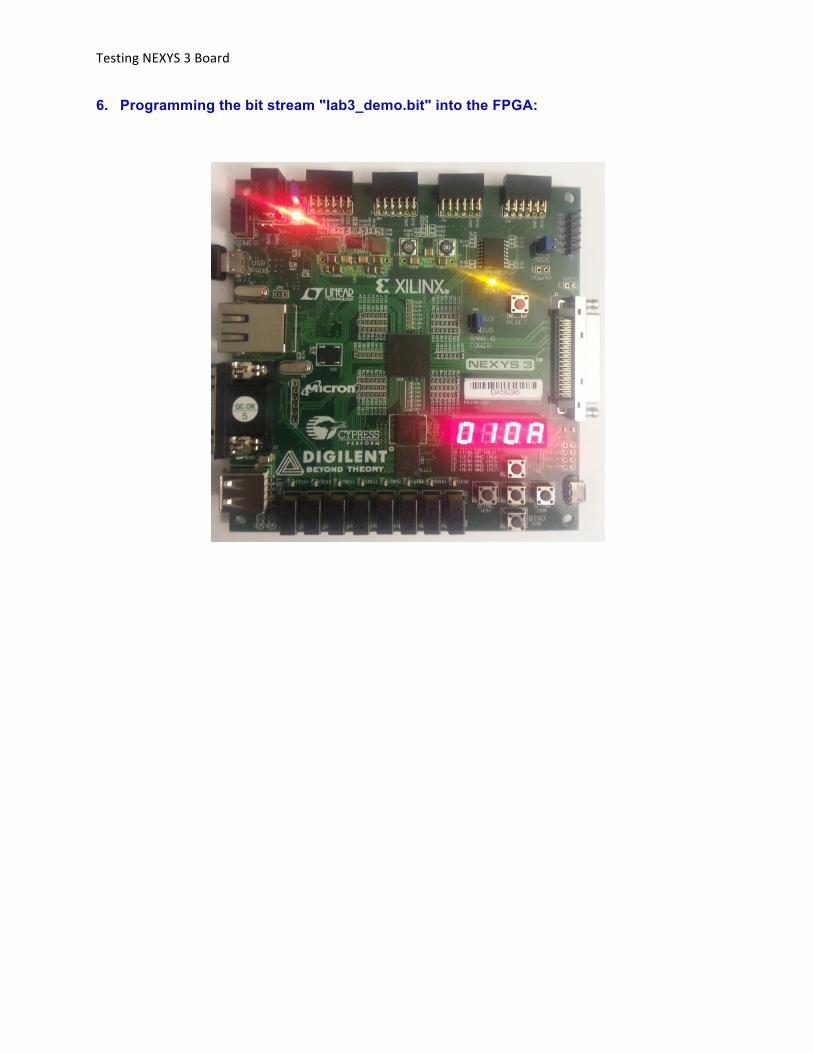
6. Programming the bit stream "lab3_demo.bit" into the FPGA: