Embed Size (px)
Citation preview
1300 Henley Court Pullman, WA 99163
509.334.6306 www.digilentinc.com
This manual applies to Rev. B; Revised October 10, 2013 Written by Mircea Dabacan, PhD, Technical University of Cluj-Napoca Romania
DOC#:502-244 Copyright Digilent, Inc. All rights reserved. Other product and company names mentioned may be trademarks of their respective owners. Page 1 of 38
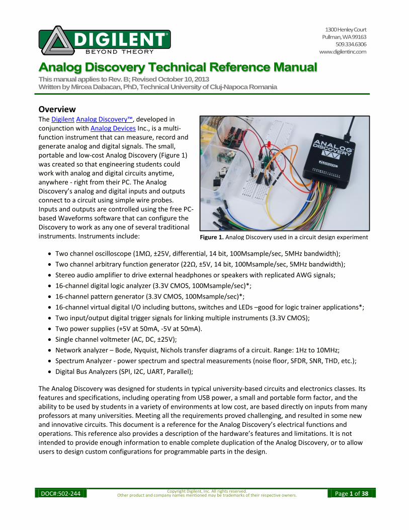
Figure 1. Analog Discovery used in a circuit design experiment
Overview The Digilent Analog Discovery™, developed in conjunction with Analog Devices Inc., is a multi-function instrument that can measure, record and generate analog and digital signals. The small, portable and low-cost Analog Discovery (Figure 1) was created so that engineering students could work with analog and digital circuits anytime, anywhere - right from their PC. The Analog Discovery’s analog and digital inputs and outputs connect to a circuit using simple wire probes. Inputs and outputs are controlled using the free PC-based Waveforms software that can configure the Discovery to work as any one of several traditional instruments. Instruments include:
Two channel oscilloscope (1MΩ, ±25V, differential, 14 bit, 100Msample/sec, 5MHz bandwidth);
Two channel arbitrary function generator (22Ω, ±5V, 14 bit, 100Msample/sec, 5MHz bandwidth);
Stereo audio amplifier to drive external headphones or speakers with replicated AWG signals;
16-channel digital logic analyzer (3.3V CMOS, 100Msample/sec)*;
16-channel pattern generator (3.3V CMOS, 100Msample/sec)*;
16-channel virtual digital I/O including buttons, switches and LEDs –good for logic trainer applications*;
Two input/output digital trigger signals for linking multiple instruments (3.3V CMOS);
Two power supplies (+5V at 50mA, -5V at 50mA).
Single channel voltmeter (AC, DC, ±25V);
Network analyzer – Bode, Nyquist, Nichols transfer diagrams of a circuit. Range: 1Hz to 10MHz;
Spectrum Analyzer - power spectrum and spectral measurements (noise floor, SFDR, SNR, THD, etc.);
Digital Bus Analyzers (SPI, I2C, UART, Parallel);
The Analog Discovery was designed for students in typical university-based circuits and electronics classes. Its features and specifications, including operating from USB power, a small and portable form factor, and the ability to be used by students in a variety of environments at low cost, are based directly on inputs from many professors at many universities. Meeting all the requirements proved challenging, and resulted in some new and innovative circuits. This document is a reference for the Analog Discovery’s electrical functions and operations. This reference also provides a description of the hardware’s features and limitations. It is not intended to provide enough information to enable complete duplication of the Analog Discovery, or to allow users to design custom configurations for programmable parts in the design.
Analog Discovery Technical Reference Manual
Copyright Digilent, Inc. All rights reserved. Other product and company names mentioned may be trademarks of their respective owners. Page 2 of 38
Architectural Overview and Block Diagram Analog Discovery’s high-level block diagram is presented in figure 2 below. The core of the Analog Discovery is the Xilinx Spartan 6 FPGA (specifically, the XC6SLX16-1L device). The Waveforms software automatically programs Discovery’s FPGA at start-up with a configuration file designed to implement a multi-function test and measurement instrument. Once programmed, the FPGA communicates with the PC-based Waveforms software via a USB2.0 connection. The Waveforms software works with the FPGA to control all the functional blocks of the Analog Discovery, including setting parameters, acquiring data, and transferring and storing data. Signals in the Analog Input block, also called the Scope, use “SC” indexes to indicate they are related to the scope block. Signals in the Analog Output block, also called AWG, use “AWG” indexes, and signals in the Digital block use a D index – all the instruments offered by Discovery and Waveforms use the circuits in these three blocks. Signal and equations also use certain naming conventions. Analog voltages are prefixed with a “V” (for Voltage), and suffixes and indexes are used in various ways: to specify the location in the signal path (IN, MUX, BUF, ADC, etc.); to indicate the related instrument (SC, AWG, etc.); to indicate the channel (1 or 2); and to indicate the type of signal (P, N, or diff). Referring to the block diagram below,
The Analog Inputs/Scope instrument block includes:
- Input Divider and Gain Control – high bandwidth input adapter/divider. High or Low Gain can be selected by the FPGA;
- Buffer – high impedance buffer; - Driver – provides appropriate signal levels and protection to the ADC. Offset voltage is added for vertical
position setting; - Scope Reference and Offset – generates and buffers reference and offset voltages for the scope stages; - ADC – the Analog to Digital Converter for both scope channels.
The Arbitrary Outputs/AWG instrument block includes:
- DAC – the Digital to Analog Converter for both AWG channels; - I/V – current to bipolar voltage converters; - Out – output stages; - Audio – audio amplifiers for headphone.
A precision Oscillator and a Clock Generator provide a high quality clock signal for the AD and DA converters.
The Digital I/O block exposes protected access to the FPGA pins assigned for the Digital Pattern Generator and Logic Analyzer.
The Power Supplies and Control block generates all internal supply voltages and user supply voltages. The control block also monitors the device power consumption for USB compliance (all power for the Analog Discovery is supplied via the USB connection). Under the FPGA control, power for unused functional blocks can be turned off.
The USB controller interfaces with the PC for programming the volatile FPGA memory after power on or when a new configuration is requested. After that, it performs the data transfer between the PC and FPGA.
The Calibration Memory stores all calibration parameters. Except for the “Probe Calibration” trimmers in the scope Input divider, the Analog Discovery includes no analog calibration circuitry. Instead, a calibration operation is performed at manufacturing (or by the user), and parameters are stored in memory. The WaveForms software uses these parameters to correct the acquired data and the generated signals.
Analog Discovery Technical Reference Manual
Copyright Digilent, Inc. All rights reserved. Other product and company names mentioned may be trademarks of their respective owners. Page 3 of 38
In the sections that follow, schematics are not shown separately for identical blocks. For example, the Scope Input Divider and Gain Selection schematic is only shown for channel 1 since the schematic for channel 2 is identical. Indexes are omitted where not relevant. As examples, in equation ( 4 ) below, does not
contain the instrument index (which by context is understood to be the Scope), nor the channel index (because the equation applies to both channels 1 and 2). In equation ( 3 ), the type index is also missing, because and refer to any of P (positive), N (negative) or diff (differential) values.
Analog Inputs
(Scope)
Analog Outputs
(AWG)
Figure 2. Analog Discovery Hardware Block Diagram
FPGA
Digital I/O
Prog Data USB ctrl
D0…D15
T0…T1 PC USB
Calibration Memory
Osc
Power Supplies and Control V+, V-
Internal power
AWG ref and offset
Input divider and gain selection
Buffer Driver
ADC Scope reference
and offset DAC
Out
Input divider and gain selection
Clock generator
I/V
Out
I/V Driver Audio
SC1
SC2
AWG1
AWG2
Buffer
Osc
Left
Right
Audio
Analog Discovery Technical Reference Manual
Copyright Digilent, Inc. All rights reserved. Other product and company names mentioned may be trademarks of their respective owners. Page 4 of 38
Scope
Scope Input Divider and Gain Selection Figure 3 shows the scope input divider and gain selection stage. Two symmetrical R-C dividers provide:
- Scope input impedance = 1MOhm || 24pF
- Two different attenuations for High Gain/Low Gain (10:1)
- Controlled capacitance, much higher than the parasitical capacitance of subsequent stages
- Constant attenuation and high CMMR over a large frequency range (trimmer adjusted)
- Protection for overvoltage (with the ESD diodes of the ADG612 inputs)
The maximum voltage rating for scope inputs is limited by C1 thru C24 to:
( 1 )
The maximum swing of the input signal to avoid signal distortion by opening the ADG612 ESD diodes is (for both Low Gain and High Gain):
( 2 )
An analog switch (ADG612) allows selecting High Gain versus Low Gain (EN_HG_SC1, EN_LG_SC1) signals from the FPGA. The P and N branches of the differential path are switched together. The ADG612 quad switch was used because it provides excellent impedance and bandwidth parameters:
- 1 pC charge injection - ±2.7 V to ±5.5 V dual-supply operation - 100 pA maximum at 25°C leakage currents - 85 Ω on resistance - Rail-to-rail switching operation
Important Note: Unlike traditional inexpensive scopes, the Analog Discovery inputs are fully differential. However, a
GND connection to the circuit under test is needed to provide a stable common mode voltage. The Analog Discovery
GND reference is connected to the USB GND. Depending on the PC powering scheme, and other PC connections
(Ethernet, audio, etc. – which might be also grounded) the Analog Discovery GND reference might be connected to
the whole system GND and ultimately to the Power Network protection (EARTH ground). The circuit under test might
be also connected to EARTH or might be floating. For safety reasons, it is the user’s responsibility to understand the
powering and grounding scheme and make sure that there is a common GND reference between the Analog
Discovery and the circuit under test, and that the common mode and differential voltages do not exceed the limits
shown in equation ( 1 ). Furthermore, for distortion-free measurements, the common mode and differential voltages
need to fit into the linear range shown in Figures 10 and 11.
For those applications which scope GND cannot be the USB ground, a USB isolation solution, such as what is
described in ADI’s CN-0160 can be used, however, this will limit things to USB full speed (12 Mbps), and will impact
the update rate (screen refresh rates, not sample rates) of the Analog Discovery.
Analog Discovery Technical Reference Manual
Copyright Digilent, Inc. All rights reserved. Other product and company names mentioned may be trademarks of their respective owners. Page 5 of 38
- Typical power consumption: <0.1 μW - TTL-/CMOS-compatible inputs - −3 dB Bandwidth 680 MHz - 5 pF each of CS, CD (ON or OFF)
The Low Gain is:
( 3 )
The Low Gain is used for input voltages: | | | | ( 4 )
The High Gain is:
( 5 )
The High Gain is used for input voltages: | | | | ( 6 )
From the
FPGA
Differential channel 1 inputs
Vmux_SC1_N Vmux_SC1_P
Figure 3. Input Divider and Gain Selection
Analog Discovery Technical Reference Manual
Copyright Digilent, Inc. All rights reserved. Other product and company names mentioned may be trademarks of their respective owners. Page 6 of 38
Scope Buffer
A non-inverting OpAmp stage provides a very high impedance as load for the input divider (Figure 4). The useful features of the AD8066 are:
- FET input amplifier - 1 pA input bias current - Low cost - High speed: 145 MHz, −3 dB bandwidth (G = +1) - 180 V/μs slew rate (G = +2) - Low noise 7 nV/√Hz (f = 10 kHz), 0.6 fA/√Hz (f = 10
kHz) - Wide supply voltage range: 5 V to 24 V - Rail-to-rail output - Low offset voltage 1.5 mV maximum - Excellent distortion specifications - SFDR −88 dBc @ 1 MHz - Low power: 6.4 mA/amplifier typical supply current - Small packaging: MSOP-8
Resistors and capacitors in the figure help to maximize the bandwidth and reduce peaking (which might be significant at unity gain). The AD8066 is supplied ± 5.5V.
The maximum input voltage swing is: ( 7 )
The maximum output voltage swing is: ( 8 )
The Gain is:
( 9 )
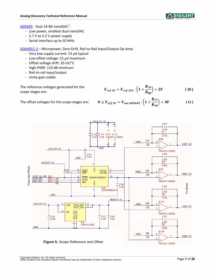
Scope reference and offset Figure 5 shows the scope voltage reference sources and offset control stage. A low noise reference is used to generate reference voltages for all the scope stages. Buffered and scaled replicas of the reference voltages are provided for the buffer stages and individually for each scope channel to minimize crosstalk. A dual channel DAC generates the offset voltages, to be added over the input signal, for vertical position. Buffers are used to provide low impedance. ADR3412ARJZ – Micropower, High Accuracy Voltage Reference:
- Initial accuracy: ±0.1% (maximum) - Low temperature coefficient: 8 ppm/°C - Low quiescent current: 100 μA (maximum) - Output noise (0.1 Hz to 10 Hz): <10 μV p-p at 1.2 V (typical)
Figure 4. Scope Buffer
Vbuf_SC1_N Vbuf_SC1_P
Vmux_SC1_N Vmux_SC1_P
Analog Discovery Technical Reference Manual
Copyright Digilent, Inc. All rights reserved. Other product and company names mentioned may be trademarks of their respective owners. Page 7 of 38
AD5643 - Dual 14-Bit nanoDAC®: - Low power, smallest dual nanoDAC - 2.7 V to 5.5 V power supply - Serial interface up to 50 MHz
ADA4051-2 – Micropower, Zero-Drift, Rail-to-Rail Input/Output Op Amp: - Very low supply current: 13 μA typical - Low offset voltage: 15 μV maximum - Offset voltage drift: 20 nV/°C - High PSRR: 110 dB minimum - Rail-to-rail input/output - Unity-gain stable
The reference voltages generated for the scope stages are:
(
) ( 10 )
The offset voltages for the scope stages are: (
) ( 11 )
Fro
m t
he F
PG
A
To
Driver
Figure 5. Scope Reference and Offset
Analog Discovery Technical Reference Manual
Copyright Digilent, Inc. All rights reserved. Other product and company names mentioned may be trademarks of their respective owners. Page 8 of 38
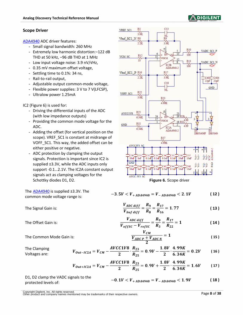
Scope Driver ADA4940 ADC driver features:
- Small signal bandwidth: 260 MHz - Extremely low harmonic distortion:−122 dB
THD at 50 kHz, −96 dB THD at 1 MHz - Low input voltage noise: 3.9 nV/√Hz, - 0.35 mV maximum offset voltage, - Settling time to 0.1%: 34 ns, - Rail-to-rail output, - Adjustable output common-mode voltage, - Flexible power supplies: 3 V to 7 V(LFCSP), - Ultralow power 1.25mA
IC2 (Figure 6) is used for:
- Driving the differential inputs of the ADC (with low impedance outputs)
- Providing the common mode voltage for the ADC.
- Adding the offset (for vertical position on the scope). VREF_SC1 is constant at midrange of VOFF_SC1. This way, the added offset can be either positive or negative.
- ADC protection by clamping the output signals. Protection is important since IC2 is supplied ±3.3V, while the ADC inputs only support -0.1…2.1V. The IC2A constant output signals act as clamping voltages for the Schottky diodes D1, D2.
The ADA4940 is supplied ±3.3V. The common mode voltage range is:
( 12 )
The Signal Gain is:
( 13 )
The Offset Gain is:
( 14 )
The Common Mode Gain is:
( 15 )
The Clamping Voltages are:
( 16 )
( 17 )
D1, D2 clamp the VADC signals to the protected levels of:
( 18 )
Figure 6. Scope driver

Analog Discovery Technical Reference Manual
Copyright Digilent, Inc. All rights reserved. Other product and company names mentioned may be trademarks of their respective owners. Page 9 of 38
Clock Generator A precision oscillator (IC31) generates a low jitter, 20MHz clock (see Figure 8). The ADF4360-9 Clock Generator PLL with Integrated VCO is configured for generating a 200MHz differential clock for the ADC and a 100MHz single ended clock for the DAC. Analog Devices ADIsimPLL software was used for designing the clock generator (see Figure 7). The PLL filter is optimized for constant frequency (low Loop Bandwidth = 50KHz and Phase Margin = 60deg.). Simulation results are shown below. The Phase jitter using a brick wall filter (10.0kHz to 100kHz) is 0.04 degrees rms.
Figure 8. Clock Generator
From FPGA
To ADC
To DAC
From FPGA
1k 10k 100k 1M 10M
Frequency (Hz)
-160
-150
-140
-130
-120
-110
-100
-90
-80
-70
-60
Ph
ase N
ois
e (
dB
c/H
z)
DIVout - Phase Noise at 100MHz
Total
Loop Filter
Chip
Ref
VCO
Figure 7. Phase Noise figure for the Clock Generator
Analog Discovery Technical Reference Manual
Copyright Digilent, Inc. All rights reserved. Other product and company names mentioned may be trademarks of their respective owners. Page 10 of 38
Scope ADC
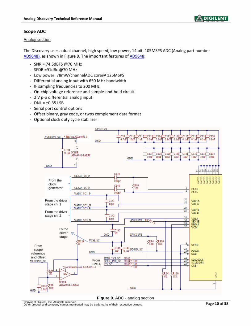
Analog section The Discovery uses a dual channel, high speed, low power, 14 bit, 105MSPS ADC (Analog part number AD9648), as shown in Figure 9. The important features of AD9648:
- SNR = 74.5dBFS @70 MHz - SFDR =91dBc @70 MHz - Low power: 78mW/channelADC core@ 125MSPS - Differential analog input with 650 MHz bandwidth - IF sampling frequencies to 200 MHz - On-chip voltage reference and sample-and-hold circuit - 2 V p-p differential analog input - DNL = ±0.35 LSB - Serial port control options - Offset binary, gray code, or twos complement data format - Optional clock duty cycle stabilizer
Figure 9. ADC - analog section
From the driver stage ch. 1 From the driver stage ch. 2
From the clock generator
To the driver stage
From FPGA
From scope
reference and offset
Analog Discovery Technical Reference Manual
Copyright Digilent, Inc. All rights reserved. Other product and company names mentioned may be trademarks of their respective owners. Page 11 of 38
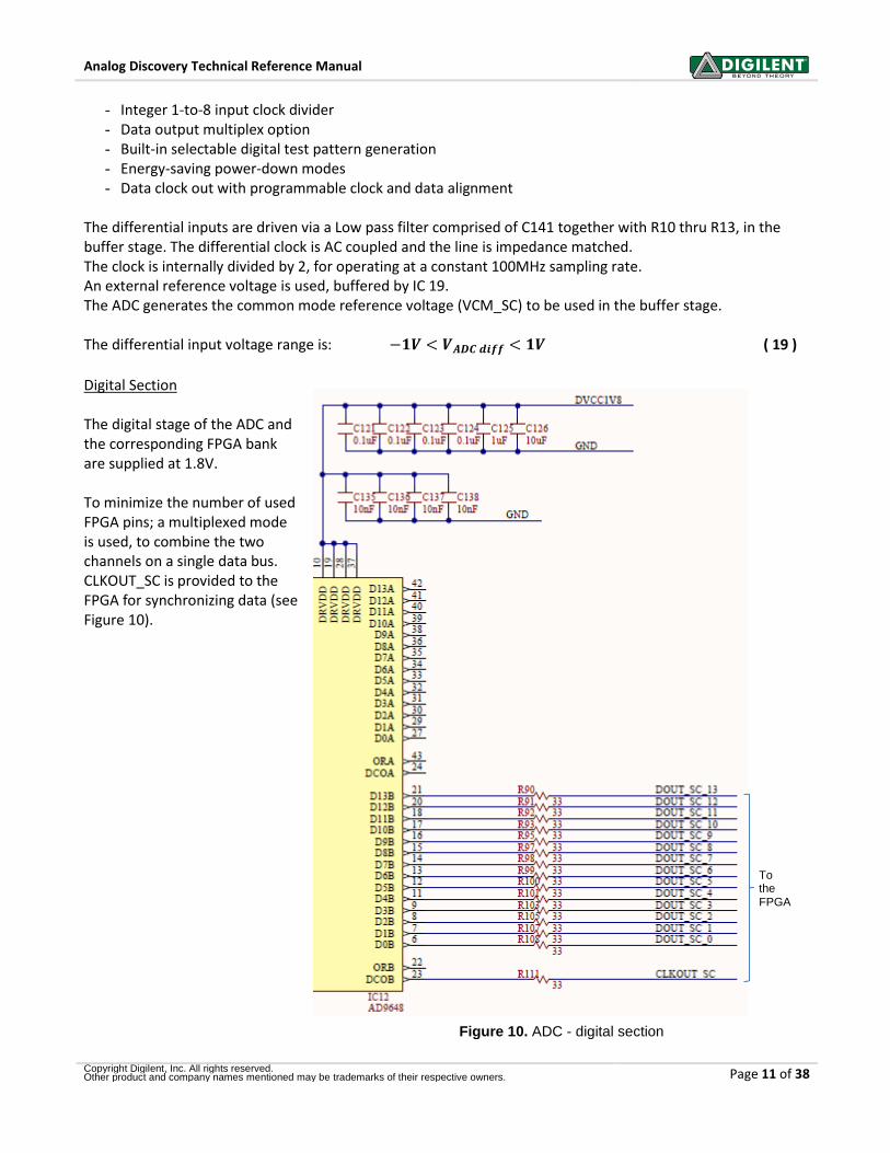
- Integer 1-to-8 input clock divider - Data output multiplex option - Built-in selectable digital test pattern generation - Energy-saving power-down modes - Data clock out with programmable clock and data alignment
The differential inputs are driven via a Low pass filter comprised of C141 together with R10 thru R13, in the buffer stage. The differential clock is AC coupled and the line is impedance matched. The clock is internally divided by 2, for operating at a constant 100MHz sampling rate. An external reference voltage is used, buffered by IC 19. The ADC generates the common mode reference voltage (VCM_SC) to be used in the buffer stage. The differential input voltage range is: ( 19 )
Digital Section The digital stage of the ADC and the corresponding FPGA bank are supplied at 1.8V. To minimize the number of used FPGA pins; a multiplexed mode is used, to combine the two channels on a single data bus. CLKOUT_SC is provided to the FPGA for synchronizing data (see Figure 10).
To the FPGA
Figure 10. ADC - digital section
Analog Discovery Technical Reference Manual
Copyright Digilent, Inc. All rights reserved. Other product and company names mentioned may be trademarks of their respective owners. Page 12 of 38
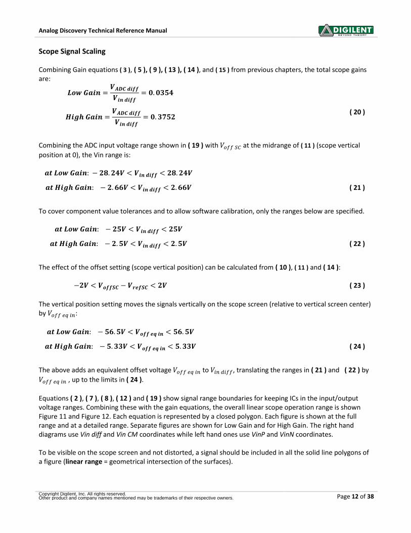
Scope Signal Scaling Combining Gain equations ( 3 ), ( 5 ), ( 9 ), ( 13 ), ( 14 ), and ( 15 ) from previous chapters, the total scope gains are:
( 20 )
Combining the ADC input voltage range shown in ( 19 ) with at the midrange of ( 11 ) (scope vertical
position at 0), the Vin range is:
( 21 )
To cover component value tolerances and to allow software calibration, only the ranges below are specified.
( 22 )
The effect of the offset setting (scope vertical position) can be calculated from ( 10 ), ( 11 ) and ( 14 ):
( 23 )
The vertical position setting moves the signals vertically on the scope screen (relative to vertical screen center) by :
( 24 )
The above adds an equivalent offset voltage to , translating the ranges in ( 21 ) and ( 22 ) by
, up to the limits in ( 24 ).
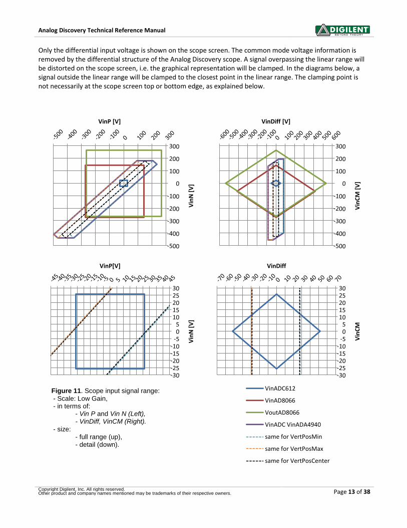
Equations ( 2 ), ( 7 ), ( 8 ), ( 12 ) and ( 19 ) show signal range boundaries for keeping ICs in the input/output voltage ranges. Combining these with the gain equations, the overall linear scope operation range is shown Figure 11 and Figure 12. Each equation is represented by a closed polygon. Each figure is shown at the full range and at a detailed range. Separate figures are shown for Low Gain and for High Gain. The right hand diagrams use Vin diff and Vin CM coordinates while left hand ones use VinP and VinN coordinates. To be visible on the scope screen and not distorted, a signal should be included in all the solid line polygons of a figure (linear range = geometrical intersection of the surfaces).
Analog Discovery Technical Reference Manual
Copyright Digilent, Inc. All rights reserved. Other product and company names mentioned may be trademarks of their respective owners. Page 13 of 38
Only the differential input voltage is shown on the scope screen. The common mode voltage information is removed by the differential structure of the Analog Discovery scope. A signal overpassing the linear range will be distorted on the scope screen, i.e. the graphical representation will be clamped. In the diagrams below, a signal outside the linear range will be clamped to the closest point in the linear range. The clamping point is not necessarily at the scope screen top or bottom edge, as explained below.
Vin
N [
V]
VinP[V]
VinADC612
VinAD8066
VoutAD8066
VinADC VinADA4940
same for VertPosMin
same for VertPosMax
same for VertPosCenter
Vin
N [
V]
VinP [V]
Vin
CM
[V
]
VinDiff [V]
Vin
CM
VinDiff
VinADC612
VinAD8066
VoutAD8066
VinADC VinADA4940
same for VertPosMin
same for VertPosMax
same for VertPosCenter
Figure 11. Scope input signal range: - Scale: Low Gain, - in terms of:
- Vin P and Vin N (Left), - VinDiff, VinCM (Right).
- size: - full range (up), - detail (down).
Analog Discovery Technical Reference Manual
Copyright Digilent, Inc. All rights reserved. Other product and company names mentioned may be trademarks of their respective owners. Page 14 of 38
The dashed lines represent the display area on the scope screen. There are three dashed rectangles in each diagram: the middle one corresponds to the vertical position set to 0 (VoffSc = 2V in equation ( 11 ). The left one shows the display area when vertical position is set to maximum (VoffSc = 4V), and the right one corresponds to the minimum (negative) vertical position (VoffSc = 0V). Any intermediate vertical position is possible, moving the displayable area (virtual dashed rectangle) to any intermediate position. A signal crossing the long side of the dashed rectangle exceeds the displayable input voltage range causing the ADC to saturate (either at zero or at Full Scale). This is represented on the scope screen with dashed line warning to the user.
Vin
N [
V]
VinP [V]
Vin
N [
V]
VinP[V]
VinADC612
VinAD8066
VoutAD8066
VinADC VinADA4940
same for VertPosMin
same for VertPosMax
same for VertPosCenter
Vin
CM
[V
]
VinDiff [V]
Vin
CM
VinDiff
VinADC612
VinAD8066
VoutAD8066
VinADC VinADA4940
same for VertPosMin
same for VertPosMax
same for VertPosCenter
Figure 12. Scope input signal range: - Scale: High Gain, - in terms of:
- Vin P and Vin N (Left), - VinDiff, VinCM (Right).
- size: - full range (up), - detail (down).
Analog Discovery Technical Reference Manual
Copyright Digilent, Inc. All rights reserved. Other product and company names mentioned may be trademarks of their respective owners. Page 15 of 38
A signal keeping within the dashed rectangle but crossing any solid line, overrides electrical limits of intermediate circuits in the signal path (see the legend of the figures). This results in distorting the signal without saturating the ADC. The software has no information about this situation and cannot warn the user with specific signal representation. It is the user’s responsibility to understand and avoid such situations. For Low Gain (Figure 11), the simple condition to stay in the linear range is to keep both positive and negative inputs in the ±26V range (as shown by equation ( 2 )). For High Gain (Figure 12), by combining equations ( 7 ) and ( 5 ) , both positive and negative inputs in must stay in the range:
( 25 ) Additionally, the differential input signal (combined with the equivalent offset voltage – vertical position) is visible only within the range:
( 26 )
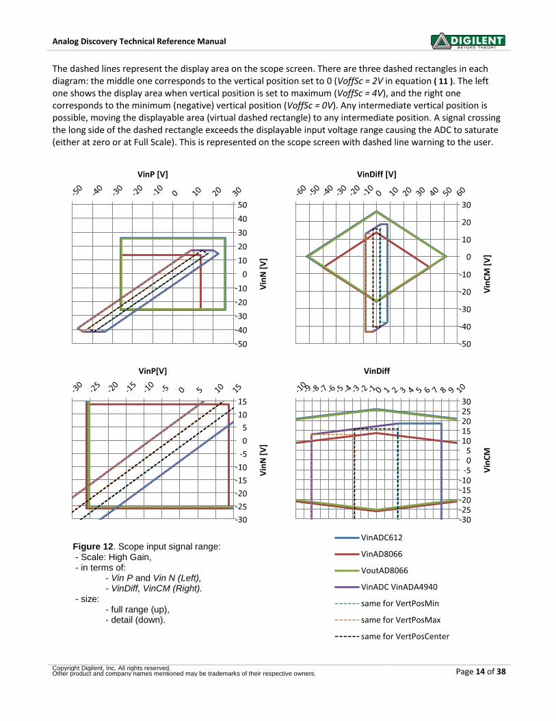
Note the difference between typical parameter values considered by the figures and the safer min/max values used for the equations. Figure 13 shows an example of a signal distorted due to a too large common mode input voltage. The grey line is the reference, not distorted, signal. The differential input voltage is a 4Vpp triangle on top of a -5V DC component. The common mode input voltage is 10V. The vertical position of the scope is set to 5V and High Gain is selected. The yellow line shows an identical signal, except the common mode input voltage is 15V.
Figure 13. Common mode input voltage limitation
Analog Discovery Technical Reference Manual
Copyright Digilent, Inc. All rights reserved. Other product and company names mentioned may be trademarks of their respective owners. Page 16 of 38
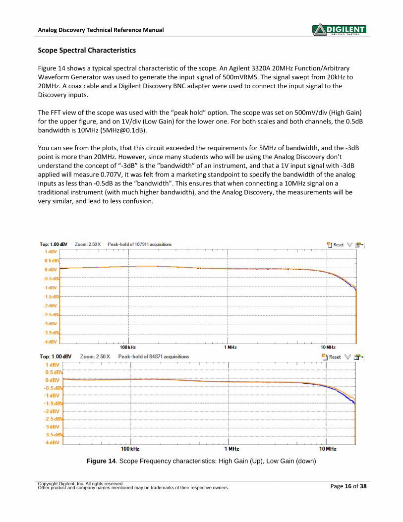
Scope Spectral Characteristics Figure 14 shows a typical spectral characteristic of the scope. An Agilent 3320A 20MHz Function/Arbitrary Waveform Generator was used to generate the input signal of 500mVRMS. The signal swept from 20kHz to 20MHz. A coax cable and a Digilent Discovery BNC adapter were used to connect the input signal to the Discovery inputs. The FFT view of the scope was used with the “peak hold” option. The scope was set on 500mV/div (High Gain) for the upper figure, and on 1V/div (Low Gain) for the lower one. For both scales and both channels, the 0.5dB bandwidth is 10MHz ([email protected]). You can see from the plots, that this circuit exceeded the requirements for 5MHz of bandwidth, and the -3dB point is more than 20MHz. However, since many students who will be using the Analog Discovery don’t understand the concept of “-3dB” is the “bandwidth” of an instrument, and that a 1V input signal with -3dB applied will measure 0.707V, it was felt from a marketing standpoint to specify the bandwidth of the analog inputs as less than -0.5dB as the “bandwidth”. This ensures that when connecting a 10MHz signal on a traditional instrument (with much higher bandwidth), and the Analog Discovery, the measurements will be very similar, and lead to less confusion.
Figure 14. Scope Frequency characteristics: High Gain (Up), Low Gain (down)
Analog Discovery Technical Reference Manual
Copyright Digilent, Inc. All rights reserved. Other product and company names mentioned may be trademarks of their respective owners. Page 17 of 38
Arbitrary Waveform Generator
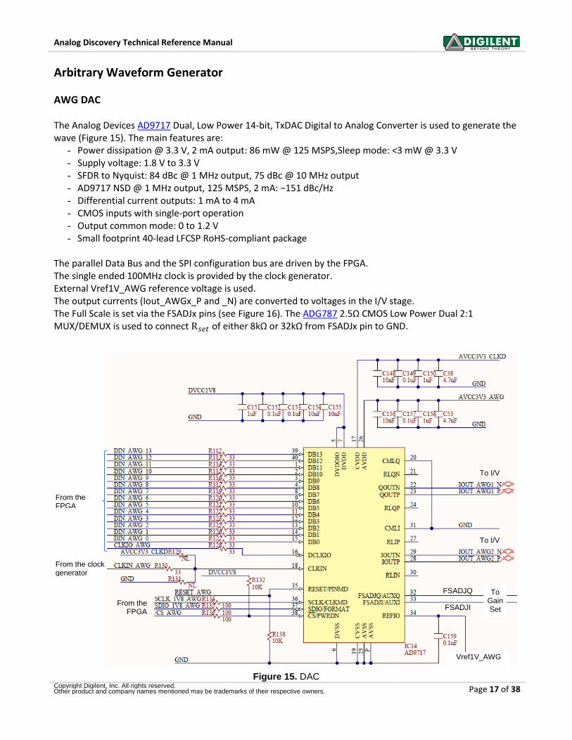
AWG DAC The Analog Devices AD9717 Dual, Low Power 14-bit, TxDAC Digital to Analog Converter is used to generate the wave (Figure 15). The main features are:
- Power dissipation @ 3.3 V, 2 mA output: 86 mW @ 125 MSPS,Sleep mode: <3 mW @ 3.3 V - Supply voltage: 1.8 V to 3.3 V - SFDR to Nyquist: 84 dBc @ 1 MHz output, 75 dBc @ 10 MHz output - AD9717 NSD @ 1 MHz output, 125 MSPS, 2 mA: −151 dBc/Hz - Differential current outputs: 1 mA to 4 mA - CMOS inputs with single-port operation - Output common mode: 0 to 1.2 V - Small footprint 40-lead LFCSP RoHS-compliant package
The parallel Data Bus and the SPI configuration bus are driven by the FPGA. The single ended 100MHz clock is provided by the clock generator. External Vref1V_AWG reference voltage is used. The output currents (Iout_AWGx_P and _N) are converted to voltages in the I/V stage. The Full Scale is set via the FSADJx pins (see Figure 16). The ADG787 2.5Ω CMOS Low Power Dual 2:1 MUX/DEMUX is used to connect of either 8kΩ or 32kΩ from FSADJx pin to GND.
From the clock generator
From the FPGA
To Gain Set
FSADJQ
FSADJI
Vref1V_AWG
To I/V
To I/V
From the FPGA
Figure 15. DAC
Analog Discovery Technical Reference Manual
Copyright Digilent, Inc. All rights reserved. Other product and company names mentioned may be trademarks of their respective owners. Page 18 of 38
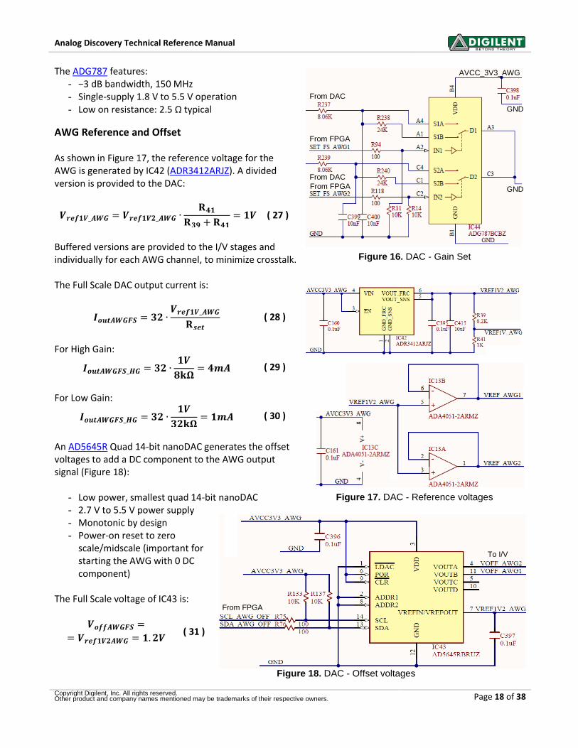
The ADG787 features: - −3 dB bandwidth, 150 MHz - Single-supply 1.8 V to 5.5 V operation - Low on resistance: 2.5 Ω typical
AWG Reference and Offset As shown in Figure 17, the reference voltage for the AWG is generated by IC42 (ADR3412ARJZ). A divided version is provided to the DAC:
( 27 )
Buffered versions are provided to the I/V stages and individually for each AWG channel, to minimize crosstalk. The Full Scale DAC output current is:
( 28 )
For High Gain:
( 29 )
For Low Gain:
( 30 )
An AD5645R Quad 14-bit nanoDAC generates the offset voltages to add a DC component to the AWG output signal (Figure 18):
- Low power, smallest quad 14-bit nanoDAC - 2.7 V to 5.5 V power supply - Monotonic by design - Power-on reset to zero
scale/midscale (important for starting the AWG with 0 DC component)
The Full Scale voltage of IC43 is:
( 31 )
AVCC_3V3_AWG
GND
GND
From DAC
From DAC
From FPGA
From FPGA
Figure 16. DAC - Gain Set
Figure 18. DAC - Offset voltages
From FPGA
To I/V
Figure 17. DAC - Reference voltages

Analog Discovery Technical Reference Manual
Copyright Digilent, Inc. All rights reserved. Other product and company names mentioned may be trademarks of their respective owners. Page 19 of 38
AWG I/V IC 15 in Figure 19 converts the DAC output currents to a bipolar voltage. Important AD8058 features:
- Low cost - 325 MHz, −3 dB bandwidth (G = +1) - 1000 V/μs slew rate - Gain flatness: 0.1 dB to 28 MHz - Low noise: 7 nV/√Hz - Low power: 5.4 mA/amplifier typical @ 5 V - Low distortion: −85 dBc@5MHz, RL=1kΩ - Wide supply range from 3 V to 12 V - Small packaging
( ) ( 32 )
Where:
[ )
( 33 ) ( ) [ ) ( )
[ ) [ ]
The Voltage range extends between:
( 34 )
Where (for High Gain respectively Low Gain):
( 35 )
Figure 19. AWG I/V and Out

Analog Discovery Technical Reference Manual
Copyright Digilent, Inc. All rights reserved. Other product and company names mentioned may be trademarks of their respective owners. Page 20 of 38
AWG Out IC16 in Figure 19 is the output stage of the AWG. AD8067 features:
- FET input: 0.6 pA input bias current - Stable for gains ≥8 for High Capacitive Load - High speed: 54 MHz@−3 dB (G = +10) - 640 V/µs slew rate - Low noise:6.6 nV/√Hz; 0.6 fA/√Hz - Low offset voltage (1.0 mV max) - Rail-to-rail output - Low distortion: SFDR 95 dBc @ 1 MHz - Low power: 6.5 mA typical supply current - Low cost; Small packaging: SOT-23-5
Matching the impedances in the inverting and non-inverting inputs of IC16:
( 36 )
( )
( 37 )
The first term in equation ( 37 ) represents the actual wave amplitude, with a range of:
( 38 )
Low Gain is used to generate low amplitude signals with improved accuracy. Any amplitude of the output signal is derivable by combining LowGain/HighGain setting (rough) with the digital signal amplitude (fine). The second term in equation ( 37 ) shows the DC component (AWG offset), with a range of (for either LowGain or HighGain):
( 39 ) AD8067 is supplied with ; to avoid saturation the user should keep the sum of AC and DC components in ( 37 ) to:
( 40 ) Only bolded ranges are used in equations ( 38 ), ( 39 ) and ( 40 ), for providing tolerance margins. The R145 PTC thermistor provides thermal protection in case of an output shortcut.
Analog Discovery Technical Reference Manual
Copyright Digilent, Inc. All rights reserved. Other product and company names mentioned may be trademarks of their respective owners. Page 21 of 38
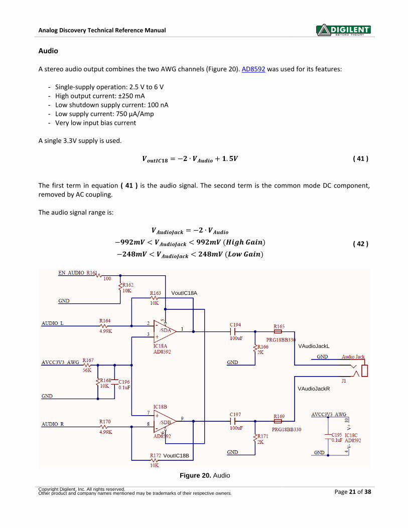
Audio A stereo audio output combines the two AWG channels (Figure 20). AD8592 was used for its features:
- Single-supply operation: 2.5 V to 6 V - High output current: ±250 mA - Low shutdown supply current: 100 nA - Low supply current: 750 μA/Amp - Very low input bias current
A single 3.3V supply is used.
( 41 ) The first term in equation ( 41 ) is the audio signal. The second term is the common mode DC component, removed by AC coupling. The audio signal range is:
( 42 ) ( )
( )
Figure 20. Audio
VoutIC18A
VoutIC18B
VAudioJackR
VAudioJackL
Analog Discovery Technical Reference Manual
Copyright Digilent, Inc. All rights reserved. Other product and company names mentioned may be trademarks of their respective owners. Page 22 of 38
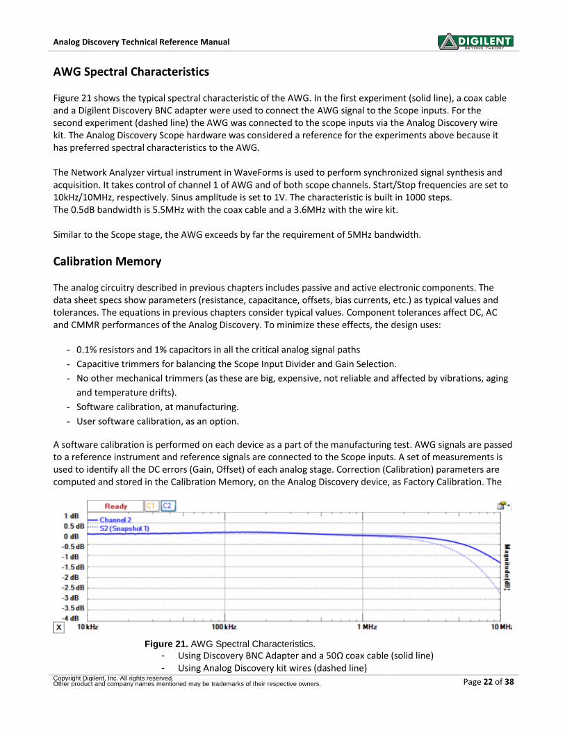
AWG Spectral Characteristics Figure 21 shows the typical spectral characteristic of the AWG. In the first experiment (solid line), a coax cable and a Digilent Discovery BNC adapter were used to connect the AWG signal to the Scope inputs. For the second experiment (dashed line) the AWG was connected to the scope inputs via the Analog Discovery wire kit. The Analog Discovery Scope hardware was considered a reference for the experiments above because it has preferred spectral characteristics to the AWG. The Network Analyzer virtual instrument in WaveForms is used to perform synchronized signal synthesis and acquisition. It takes control of channel 1 of AWG and of both scope channels. Start/Stop frequencies are set to 10kHz/10MHz, respectively. Sinus amplitude is set to 1V. The characteristic is built in 1000 steps. The 0.5dB bandwidth is 5.5MHz with the coax cable and a 3.6MHz with the wire kit. Similar to the Scope stage, the AWG exceeds by far the requirement of 5MHz bandwidth.
Calibration Memory The analog circuitry described in previous chapters includes passive and active electronic components. The data sheet specs show parameters (resistance, capacitance, offsets, bias currents, etc.) as typical values and tolerances. The equations in previous chapters consider typical values. Component tolerances affect DC, AC and CMMR performances of the Analog Discovery. To minimize these effects, the design uses:
- 0.1% resistors and 1% capacitors in all the critical analog signal paths
- Capacitive trimmers for balancing the Scope Input Divider and Gain Selection.
- No other mechanical trimmers (as these are big, expensive, not reliable and affected by vibrations, aging
and temperature drifts).
- Software calibration, at manufacturing.
- User software calibration, as an option.
A software calibration is performed on each device as a part of the manufacturing test. AWG signals are passed to a reference instrument and reference signals are connected to the Scope inputs. A set of measurements is used to identify all the DC errors (Gain, Offset) of each analog stage. Correction (Calibration) parameters are computed and stored in the Calibration Memory, on the Analog Discovery device, as Factory Calibration. The
Figure 21. AWG Spectral Characteristics.
- Using Discovery BNC Adapter and a 50Ω coax cable (solid line) - Using Analog Discovery kit wires (dashed line)

Analog Discovery Technical Reference Manual
Copyright Digilent, Inc. All rights reserved. Other product and company names mentioned may be trademarks of their respective owners. Page 23 of 38
WaveForms software allows the user performing an in-house calibration and overwrite the Calibration Data. Returning to Factory Calibration is always possible. The WaveForms Software reads the calibration parameters from the connected Analog Discovery and uses them to correct both generated and acquired signals.
Digital I/O Figure 22 shows half of the Digital I/O pin circuitry (the other half is symmetrical). J3 is the Analog Discovery user signal connector. General purpose FPGA I/O pins are used for Analog Discovery Digital I/O. FPGA pins are set to SLOW slew rate and 4mA drive strength, with no internal pull. PTC thermistors provide thermal protection in case of shortcuts. Schottky Diodes double the internal FPGA ESD protection diodes for increasing the acceptable current in case of overvoltage. Nominal resistance of the PTCs (220Ω) and parasitical capacitance of the Schottky diodes (2.2pF) and FPGA pins (10pF) limit the bandwidth of the input pins. For output pins, the PTCs and the load impedance limit the bandwidth and power. Input and output pins are LVCMOS3V3. Inputs are 5V tolerant. Overvoltage up to ±20V is supported.
Figure 22. Digital I/O
To
FP
GA
Analog Discovery Technical Reference Manual
Copyright Digilent, Inc. All rights reserved. Other product and company names mentioned may be trademarks of their respective owners. Page 24 of 38
Power Supplies and Control This block includes all power monitoring and control circuitry, internal power supplies and user power supplies.
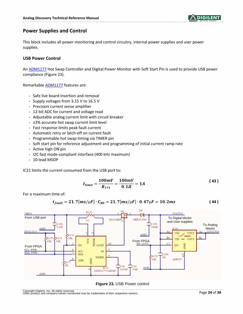
USB Power Control An ADM1177 Hot Swap Controller and Digital Power Monitor with Soft Start Pin is used to provide USB power compliance (Figure 23). Remarkable ADM1177 features are:
- Safe live board insertion and removal - Supply voltages from 3.15 V to 16.5 V - Precision current sense amplifier - 12-bit ADC for current and voltage read - Adjustable analog current limit with circuit breaker - ±3% accurate hot swap current limit level - Fast response limits peak fault current - Automatic retry or latch-off on current fault - Programmable hot swap timing via TIMER pin - Soft start pin for reference adjustment and programming of initial current ramp rate - Active high ON pin - I2C fast mode-compliant interface (400 kHz maximum) - 10-lead MSOP
IC21 limits the current consumed from the USB port to:
( 43 )
For a maximum time of:
[ ] [ ] ( 44 )
Figure 23. USB Power control
From FPGA
From USB port
From FPGA
To Analog blocks
To Digital blocks and User supplies
Analog Discovery Technical Reference Manual
Copyright Digilent, Inc. All rights reserved. Other product and company names mentioned may be trademarks of their respective owners. Page 25 of 38
If the consumed current does not fall below before , IC21 turns off Q2. A hot swap retry is initiated
after:
[ ] [
] ( 45 )
To avoid big in-rush currents at hot swap, Soft Start circuitry limits the current slope to:
( 46 )
If the current drops below before , normal operation begins.
During normal operation, the FPGA constantly reads the current value (Optionally displayed on Main Window/Discovery). If a value of 600mA is reached and Overcurrent protection is enabled (Main Window/Device/Settings/ Overcurrent protection), WaveForms turns off IC20 (ADP197), IC26, and IC27 shown in Figure 25, disabling the analog blocks and user power supplies. The FPGA and USB circuitry remain functional, for communicating with the WaveForms software. ADP197 main features:
- Low RDSon of 12mΩ - Low input voltage range: 1.8V to 5.5V - 1.2V logic compatible enable logic - Overtemperature protection - Ultrasmall 1.0mmX1.5mm, 6 ball, 0.5mm pitch WLCSP
The Analog Discovery user pins are overvoltage protected. Overvoltage (or ESD) diodes short when a user pin is overdriven by the external circuitry (Circuit Under Test), back powering the input/output block and all the circuits sharing the same internal power supply. If the back-powered energy is higher than the used energy, the bi-directional power supply recovers the difference and delivers it to the previous node in the power chain. Eventually, the back-powering energy could arrive to the USB VBUS, raising the voltage above the 5V nominal value. D5 in Figure 23 protects the PC USB port against such a situation.
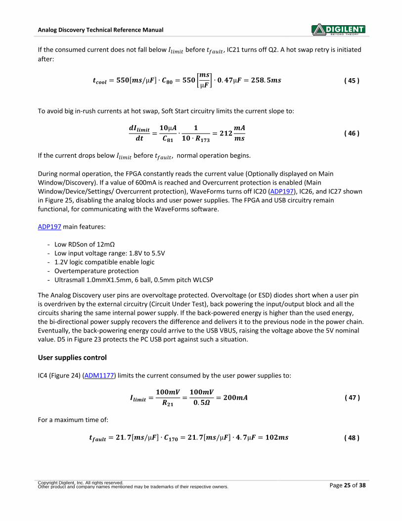
User supplies control IC4 (Figure 24) (ADM1177) limits the current consumed by the user power supplies to:
( 47 )
For a maximum time of:
[ ] [ ] ( 48 )
Analog Discovery Technical Reference Manual
Copyright Digilent, Inc. All rights reserved. Other product and company names mentioned may be trademarks of their respective owners. Page 26 of 38
If the consumed current does not fall below before , IC21 turns off Q2. A hot swap retry is initiated
after:
[ ] [ ] ( 49 ) Soft Start is not used; C183 is a No Load. If the current drops below before , normal operation begins.
The current limited by equation ( 47 ) supplies both positive and negative user power supplies. After considering the efficiency of the user supply stages, about 100mA is available for user in both supplies together.
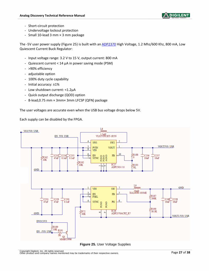
User Voltage Supplies The +5v user power supply (Figure 25) is implemented around an ADP2503-5 600mA, 2.5MHz Buck-Boost DC-to-DC Converter. Main features:
- 1 mm height profile
- Compact PCB footprint
- Seamless transition between modes
- 38 μA typical quiescent current
- 2.5 MHz operation enables 1.5 μH inductor
- Input voltage: 2.3 V to 5.5 V
- Fixed output voltage: 5.0 V
- Boost converter configuration with load disconnect
- Forced fixed frequency operation mode
- Internal compensation
- Soft start
- Enable/shutdown logic input
- Overtemperature protection
Figure 24. User supplies control
Analog Discovery Technical Reference Manual
Copyright Digilent, Inc. All rights reserved. Other product and company names mentioned may be trademarks of their respective owners. Page 27 of 38
- Short-circuit protection - Undervoltage lockout protection - Small 10-lead 3 mm × 3 mm package
The -5V user power supply (Figure 25) is built with an ADP2370 High Voltage, 1.2 Mhz/600 Khz, 800 mA, Low Quiescent Current Buck Regulator:
- Input voltage range: 3.2 V to 15 V, output current: 800 mA
- Quiescent current < 14 µA in power saving mode (PSM)
- >90% efficiency
- adjustable option
- 100% duty cycle capability
- Initial accuracy: ±1%
- Low shutdown current: <1.2µA
- Quick output discharge (QOD) option
- 8-lead,0.75 mm × 3mm× 3mm LFCSP (QFN) package
The user voltages are accurate even when the USB bus voltage drops below 5V. Each supply can be disabled by the FPGA.
Figure 25. User Voltage Supplies
Analog Discovery Technical Reference Manual
Copyright Digilent, Inc. All rights reserved. Other product and company names mentioned may be trademarks of their respective owners. Page 28 of 38
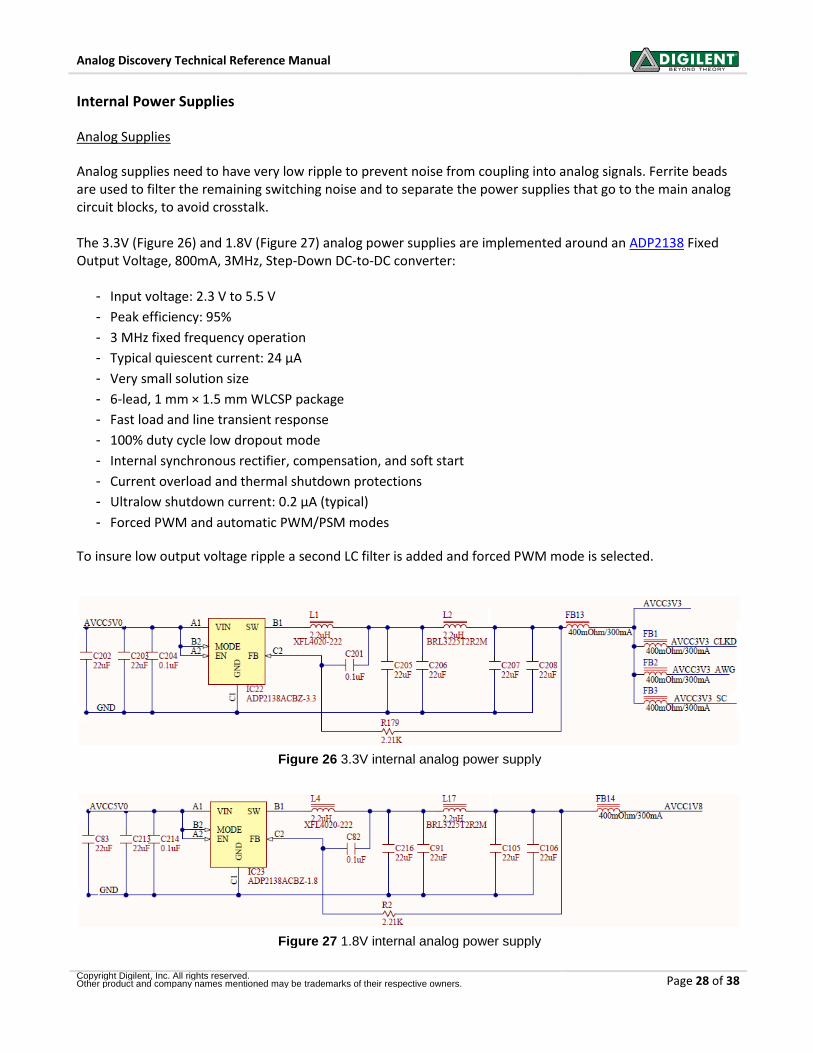
Internal Power Supplies Analog Supplies Analog supplies need to have very low ripple to prevent noise from coupling into analog signals. Ferrite beads are used to filter the remaining switching noise and to separate the power supplies that go to the main analog circuit blocks, to avoid crosstalk. The 3.3V (Figure 26) and 1.8V (Figure 27) analog power supplies are implemented around an ADP2138 Fixed Output Voltage, 800mA, 3MHz, Step-Down DC-to-DC converter:
- Input voltage: 2.3 V to 5.5 V
- Peak efficiency: 95%
- 3 MHz fixed frequency operation
- Typical quiescent current: 24 μA
- Very small solution size
- 6-lead, 1 mm × 1.5 mm WLCSP package
- Fast load and line transient response
- 100% duty cycle low dropout mode
- Internal synchronous rectifier, compensation, and soft start
- Current overload and thermal shutdown protections
- Ultralow shutdown current: 0.2 μA (typical)
- Forced PWM and automatic PWM/PSM modes
To insure low output voltage ripple a second LC filter is added and forced PWM mode is selected.
Figure 26 3.3V internal analog power supply
Figure 27 1.8V internal analog power supply
Analog Discovery Technical Reference Manual
Copyright Digilent, Inc. All rights reserved. Other product and company names mentioned may be trademarks of their respective owners. Page 29 of 38
The -3.3V analog power supply (Figure 28) is implemented with the ADP2301 Step-Down regulator in an inverting Buck-Boost configuration. See application Note AN-1083: Designing an Inverting Buck Boost Using the ADP2300 and ADP2301. The ADP2301 features:
- 1.2 A maximum load current
- ±2% output accuracy over temperature range
- Wide input voltage range: 3.0 V to 20 V
- 1.4 MHz switching frequency
- High efficiency up to 91%
- Current-mode control architecture
- Output voltage from 0.8 V to 0.85 × VIN
- Automatic PFM/PWM mode switching
- Integrated high-side MOSFET
- Integrated bootstrap diode
- Internal compensation and soft start
- Undervoltage lockout (UVLO)
- Overcurrent protection (OCP) and thermal shutdown (TSD)
- Available in ultrasmall, 6-lead TSOT package
The Output voltage is set with an external resistor divider from Vout to FB:
( 50 )
Choosing :
( 51 )
Closest standard value is The 5.5V and -5.5V supplies (Figure 29) are created with a Sepic-Cuk topology, built around a single ADP1612 Step-Up DC-to DC converter. Main features:
- 1.4A current limit
- Minimum input voltage 1.8V
- Pin-selectable 650 kHz or 1.3 MHz PWM frequency
Figure 28 -3.3V internal analog power supply
Analog Discovery Technical Reference Manual
Copyright Digilent, Inc. All rights reserved. Other product and company names mentioned may be trademarks of their respective owners. Page 30 of 38
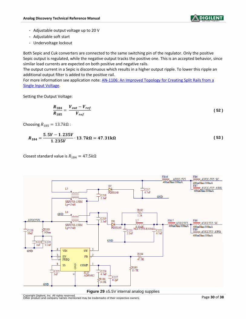
- Adjustable output voltage up to 20 V
- Adjustable soft start
- Undervoltage lockout
Both Sepic and Cuk converters are connected to the same switching pin of the regulator. Only the positive Sepic output is regulated, while the negative output tracks the positive one. This is an accepted behavior, since similar load currents are expected on both positive and negative rails. The output current in a Sepic is discontinuous which results in a higher output ripple. To lower this ripple an additional output filter is added to the positive rail. For more information see application note: AN-1106: An Improved Topology for Creating Split Rails from a Single Input Voltage. Setting the Output Voltage:
( 52 )
Choosing :
( 53 )
Closest standard value is
Figure 29 ±5.5V internal analog supplies
Analog Discovery Technical Reference Manual
Copyright Digilent, Inc. All rights reserved. Other product and company names mentioned may be trademarks of their respective owners. Page 31 of 38
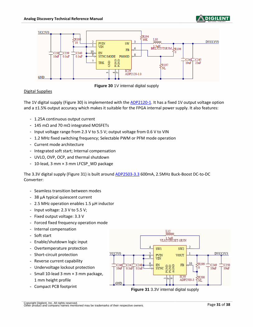
Digital Supplies The 1V digital supply (Figure 30) is implemented with the ADP2120-1. It has a fixed 1V output voltage option and a ±1.5% output accuracy which makes it suitable for the FPGA internal power supply. It also features:
- 1.25A continuous output current
- 145 mΩ and 70 mΩ integrated MOSFETs
- Input voltage range from 2.3 V to 5.5 V; output voltage from 0.6 V to VIN
- 1.2 MHz fixed switching frequency; Selectable PWM or PFM mode operation
- Current mode architecture
- Integrated soft start; Internal compensation
- UVLO, OVP, OCP, and thermal shutdown
- 10-lead, 3 mm × 3 mm LFCSP_WD package
The 3.3V digital supply (Figure 31) is built around ADP2503-3.3 600mA, 2.5MHz Buck-Boost DC-to-DC Converter:
- Seamless transition between modes
- 38 μA typical quiescent current
- 2.5 MHz operation enables 1.5 μH inductor
- Input voltage: 2.3 V to 5.5 V;
- Fixed output voltage: 3.3 V
- Forced fixed frequency operation mode
- Internal compensation
- Soft start
- Enable/shutdown logic input
- Overtemperature protection
- Short-circuit protection
- Reverse current capability
- Undervoltage lockout protection
- Small 10-lead 3 mm × 3 mm package,
1 mm height profile
- Compact PCB footprint
Figure 30 1V internal digital supply
Figure 31 3.3V internal digital supply
Analog Discovery Technical Reference Manual
Copyright Digilent, Inc. All rights reserved. Other product and company names mentioned may be trademarks of their respective owners. Page 32 of 38
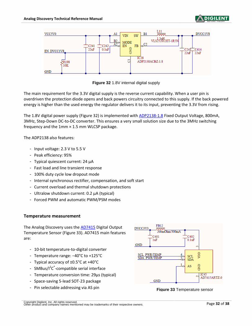
The main requirement for the 3.3V digital supply is the reverse current capability. When a user pin is overdriven the protection diode opens and back powers circuitry connected to this supply. If the back powered energy is higher than the used energy the regulator delivers it to its input, preventing the 3.3V from rising. The 1.8V digital power supply (Figure 32) is implemented with ADP2138-1.8 Fixed Output Voltage, 800mA, 3MHz, Step-Down DC-to-DC converter. This ensures a very small solution size due to the 3MHz switching frequency and the 1mm × 1.5 mm WLCSP package. The ADP2138 also features:
- Input voltage: 2.3 V to 5.5 V
- Peak efficiency: 95%
- Typical quiescent current: 24 μA
- Fast load and line transient response
- 100% duty cycle low dropout mode
- Internal synchronous rectifier, compensation, and soft start
- Current overload and thermal shutdown protections
- Ultralow shutdown current: 0.2 μA (typical)
- Forced PWM and automatic PWM/PSM modes
Temperature measurement The Analog Discovery uses the AD7415 Digital Output Temperature Sensor (Figure 33). AD7415 main features are:
- 10-bit temperature-to-digital converter
- Temperature range: −40°C to +125°C
- Typical accuracy of ±0.5°C at +40°C
- SMBus/I2C®-compatible serial interface
- Temperature conversion time: 29μs (typical)
- Space-saving 5-lead SOT-23 package
- Pin selectable addressing via AS pin
Figure 32 1.8V internal digital supply
Figure 33 Temperature sensor
Analog Discovery Technical Reference Manual
Copyright Digilent, Inc. All rights reserved. Other product and company names mentioned may be trademarks of their respective owners. Page 33 of 38
USB Controller The USB interface performs two tasks:
- Programming the FPGA: There is no non-volatile FPGA configuration memory on the Analog Discovery.
The WaveForms software identifies the connected device and downloads an appropriate .bit file at
power-up, via a Digilent USB-JTAG interface. Adept run-time is used for low level protocols.
- Data exchange: All instrument configuration data, acquired data and status information is handled via a
Digilent synchronous parallel bus and USB interface. Speed up to 20MB/sec. is reached, depending on
USB port type and load as well as PC performance.
FPGA The core of the Analog Discovery is the Xilinx the Spartan 6 FPGA circuit XC6SLX16-1L. The configured logic performs:
- Clock management (12MHz and 60MHz for USB communication, 100MHz for data sampling) - Acquisition control and Data Storage (Scope and Logic Analyzer) - Analog Signal synthesis (look-up tables, AM/FM modulation for AWG) - Digital signal synthesis (for pattern generator) - Trigger system (trigger detection and distribution for all instruments ) - Power supplies control and instruments enabling - Power and temperature monitoring - Calibration memory control - Communication with the PC (settings, status data)
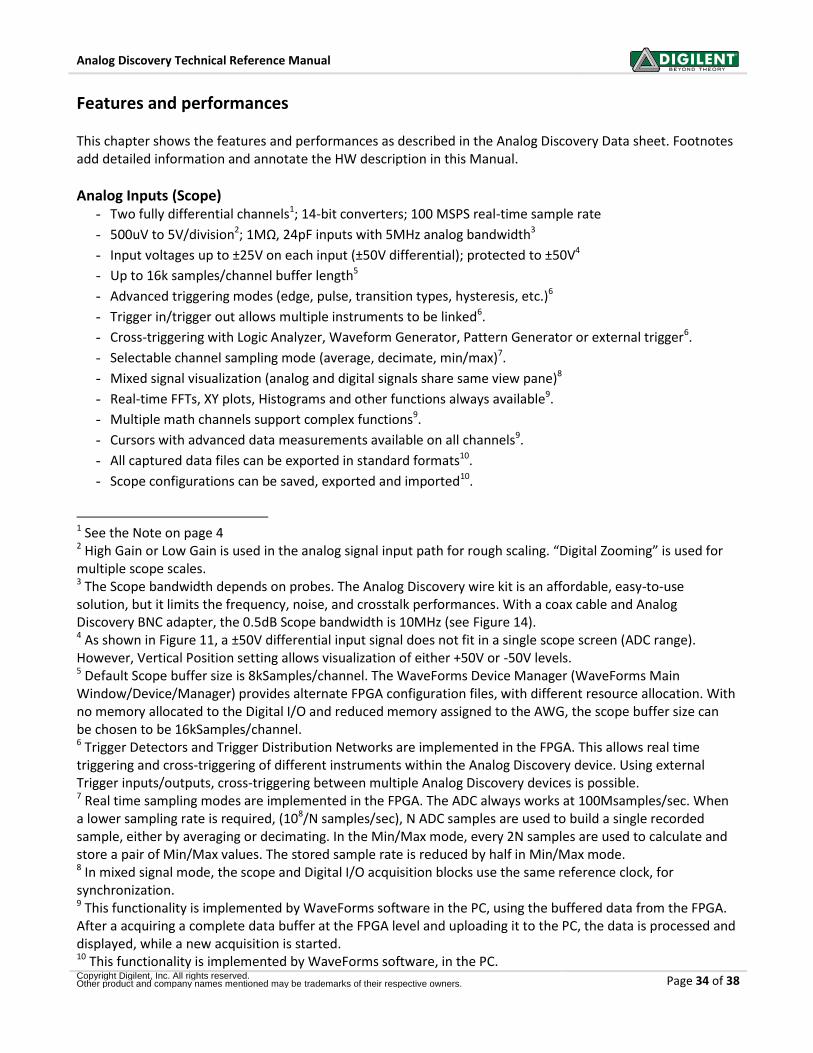
Block and Distributed RAM of the FPGA are used for signal synthesis and acquisition. Multiple configuration files are available through WaveForms software, to allocate the RAM resources according the application. A detail of trigger system is shown in Figure 34. Each instrument generates a trigger signal when a trigger condition is met. Each trigger signal (including external triggers) can trigger any instrument and drive the external trigger outputs. This way, all the instruments can synchronize to each other.
Trig Ext
DI/O ADC
Oscilloscope
Trigger Detector
Control
Analyzer
Trigger Detector
Control
Patterns
Control
Trig
ge
r sig
nals
bu
s
Board ON
WaveGen 1
Control
Figure 34. FPGA configuration trigger block diagram
Analog Discovery Technical Reference Manual
Copyright Digilent, Inc. All rights reserved. Other product and company names mentioned may be trademarks of their respective owners. Page 34 of 38
Features and performances This chapter shows the features and performances as described in the Analog Discovery Data sheet. Footnotes add detailed information and annotate the HW description in this Manual.
Analog Inputs (Scope) - Two fully differential channels1; 14-bit converters; 100 MSPS real-time sample rate
- 500uV to 5V/division2; 1MΩ, 24pF inputs with 5MHz analog bandwidth3
- Input voltages up to ±25V on each input (±50V differential); protected to ±50V4
- Up to 16k samples/channel buffer length5
- Advanced triggering modes (edge, pulse, transition types, hysteresis, etc.)6
- Trigger in/trigger out allows multiple instruments to be linked6.
- Cross-triggering with Logic Analyzer, Waveform Generator, Pattern Generator or external trigger6.
- Selectable channel sampling mode (average, decimate, min/max)7.
- Mixed signal visualization (analog and digital signals share same view pane)8
- Real-time FFTs, XY plots, Histograms and other functions always available9.
- Multiple math channels support complex functions9.
- Cursors with advanced data measurements available on all channels9.
- All captured data files can be exported in standard formats10.
- Scope configurations can be saved, exported and imported10.
1 See the Note on page 4 2 High Gain or Low Gain is used in the analog signal input path for rough scaling. “Digital Zooming” is used for multiple scope scales. 3 The Scope bandwidth depends on probes. The Analog Discovery wire kit is an affordable, easy-to-use solution, but it limits the frequency, noise, and crosstalk performances. With a coax cable and Analog Discovery BNC adapter, the 0.5dB Scope bandwidth is 10MHz (see Figure 14). 4 As shown in Figure 11, a ±50V differential input signal does not fit in a single scope screen (ADC range). However, Vertical Position setting allows visualization of either +50V or -50V levels. 5 Default Scope buffer size is 8kSamples/channel. The WaveForms Device Manager (WaveForms Main Window/Device/Manager) provides alternate FPGA configuration files, with different resource allocation. With no memory allocated to the Digital I/O and reduced memory assigned to the AWG, the scope buffer size can be chosen to be 16kSamples/channel. 6 Trigger Detectors and Trigger Distribution Networks are implemented in the FPGA. This allows real time triggering and cross-triggering of different instruments within the Analog Discovery device. Using external Trigger inputs/outputs, cross-triggering between multiple Analog Discovery devices is possible. 7 Real time sampling modes are implemented in the FPGA. The ADC always works at 100Msamples/sec. When a lower sampling rate is required, (108/N samples/sec), N ADC samples are used to build a single recorded sample, either by averaging or decimating. In the Min/Max mode, every 2N samples are used to calculate and store a pair of Min/Max values. The stored sample rate is reduced by half in Min/Max mode. 8 In mixed signal mode, the scope and Digital I/O acquisition blocks use the same reference clock, for synchronization. 9 This functionality is implemented by WaveForms software in the PC, using the buffered data from the FPGA. After a acquiring a complete data buffer at the FPGA level and uploading it to the PC, the data is processed and displayed, while a new acquisition is started. 10 This functionality is implemented by WaveForms software, in the PC.
Analog Discovery Technical Reference Manual
Copyright Digilent, Inc. All rights reserved. Other product and company names mentioned may be trademarks of their respective owners. Page 35 of 38
Analog Outputs (Arbitrary Waveform Generator) - Two channels; 14-bit converters; 100 MSPS real-time sample rate11.
- Single-ended waveforms with offset control and up to ±5 V amplitude12.
- 5MHz analog bandwidth13 and up to 16k samples/channel14.
- Easily defined standard waveforms (sine, triangle, sawtooth, etc.)
- Easily defined sweeps, envelopes, AM and FM modulation15.
- User-defined arbitrary waveforms can be defined within WaveForms software user interface or using
standard tools (e.g. Excel) 10.
- Cross-triggering between Analog input channels, Logic Analyzer, Pattern Generator or external trigger6.
Logic Analyzer - 16 signals shared between analyzer, pattern generator, and discrete I/O16
- 100 MSPS, with buffers supporting up to 16K transitions per pin17.
- LVCMOS (3.3V) logic level inputs
- Multiple trigger options including pin change, bus pattern, etc6.
- Trigger in/trigger out allows multiple instruments to be linked6.
- Cross-triggering between Analog input channels, Logic Analyzer, Pattern Generator or external trigger6.
- Interpreter for SPI, I2C, UART, Parallel bus9.
- Captured signals can be saved and exported in standard file formats10.
11 The AWG DAC always works at 100Msamples/sec. When a lower sampling rate is required, (108/N samples/sec), each sample is sent N times to the DAC. 12 The AWG output voltage is limited to ±5V. This refers to the sum of AC signal and DC offset. 13 The AWG bandwidth depends on probes. Analog Discovery wire kit is an affordable, easy-to-use solution, but it limits the frequency, noise, and crosstalk performances. With a coax cable and Analog Discovery BNC adapter, the 0.5dB AWG bandwidth is 5.5MHz (3.6MHz with the wire kit) (see Figure 21). 14 Default AWG buffer size is 4kSamples/channel. The WaveForms Device Manager (WaveForms Main Window/Device/Manager) provides alternate FPGA configuration files, with different resources allocation. With no memory allocated to the Digital I/O and reduced memory assigned to the Scope, the AWG buffer size can be chosen to be 16kSamples/channel. 15 Real time implemented in the FPGA configuration. 16 All digital I/O pins are always available as inputs, to be acquired and displayed in the Logic Analyzer and Static I/O WaveForms instruments. The user selects which pins are also used as outputs, by the Pattern Generator or Static I/O instruments. When a signal is driven by both Pattern Generator and Static I/O instruments, the Static I/O instrument has priority, except if Static I/O attempts to drive a HiZ value. 17 Default Logic Analyzer buffer size is 4kSamples/channel. The WaveForms Device Manager (WaveForms Main Window/Device/Manager) provides alternate FPGA configuration files, with different resource allocation. With no memory allocated to the Scope and AWG, the Logic Analyzer buffer size can be chosen to be 16kSamples/channel.
Analog Discovery Technical Reference Manual
Copyright Digilent, Inc. All rights reserved. Other product and company names mentioned may be trademarks of their respective owners. Page 36 of 38
Digital Pattern Generator - 16 signals shared between analyzer, pattern generator, and discrete I/O16.
- 100 MSPS,
- Algorithmic pattern generator (no memory buffers used)15.
- Custom pattern editor with buffers supporting up to 16K transitions per pin18.
- 3.3V outputs
- Data file import/export using standard formats10.
- Customized visualization options for signals and busses10.
Digital I/O - 16 signals shared between analyzer, pattern generator, and discrete I/O16.
- LVCMOS (3.3 V) logic level inputs and outputs
- PC-based virtual I/O devices (buttons, switches & displays) drive physical pins10.
- Customized visualization options available10.
Power Supplies - Two fixed power supplies derive power from USB port
- +5V up to 50mA and -5V up to 50mA (100mA total)
Network Analyzer19 - Waveform generator drives circuits with swept sine waves up to 10MHz
- Input waveforms settable from 1Hz to 10MHz, with 5 to 1000 steps10.
- Settable input amplitude and offset
- Analog input records response at each frequency10.
- Response magnitude and phase delay displayed in Bode, Nichols, or Nyquist formats10.
Voltmeters20 - Two independent meters (shared with Analog input channels)
- Automatic measurements include DC, AC RMS and True RMS values10.
- Single-ended and differential measurement capability
- Up to ±25V on each pin (±50V max peak-peak)
- Auto-range feature selects best gain range10.
18 Default Pattern Generator buffer size is 1kSamples/channel. The WaveForms Device Manager (WaveForms Main Window/Device/Manager) provides alternate FPGA configuration files, with different resources allocation. With no memory allocated to the Scope and AWG, the Pattern Generator buffer size can be chosen to be 16kSamples/channel. 19 The Network Analyzer instrument in WaveForms uses Analog Outputs (AWG) channel1 and Analog Inputs (Scope) hardware resources. When it starts running, all other instruments using the same HW resources (competing instruments: AWG channel 1, Scope, Voltmeters, Spectrum Analyzer) are forced to a BUSY state. When running a competing instrument, the Network Analyzer is forced to a BUSY state. 20 The Voltmeter instrument in WaveForms uses Analog Inputs (Scope) Hardware resources competing with other WaveForms instruments (Scope, Network Analyzer, Spectrum Analyzer). When it starts running, the competing instruments are forced to a BUSY state. When running a competing instrument, the Voltmeter is forced in BUSY state.
Analog Discovery Technical Reference Manual
Copyright Digilent, Inc. All rights reserved. Other product and company names mentioned may be trademarks of their respective owners. Page 37 of 38
Spectrum Analyzer21 - Performs FFT or CZT algorithm on analog input channels and displays power spectrum10.
- Frequency range adjustments in center/span or start/stop modes10.
- Linear or logarithmic frequency scale10.
- Peak tracking option finds peak power and adjusts display to keep peak in center of display10.
- Vertical axis supports voltage-peak, voltage-RMS, dBV and dBu display options10.
- Windowing options include rectangular, triangular, hamming, Cosine, and many others10.
- Cursors and automatic measurements including noise floor, SFDR, SNR, THD and many others10.
- Data file import/export using standard formats10.
Other features - USB powered; all needed cables included
- High-speed USB2 interface for fast data transfer
- Waveform Generator output can be played on stereo audio jack
- Two external trigger pins can link triggers across multiple devices6.
- Cross triggering between instruments6.
- Help screens, including contextual help10.
- New! Supported by MATLAB and the MATLAB student edition
- Instruments and workspaces can be individually configured; configurations can be exported10.
21 The Spectrum Analyzer instrument in WaveForms uses Analog Inputs (Scope) Hardware resources competing with other WaveForms instruments (Scope, Network Analyzer, Voltmeter). When it starts running, the competing instruments are forced to a BUSY state. When running a competing instrument, the Spectrum Analyzer is forced to a BUSY state.
Analog Discovery Technical Reference Manual
Copyright Digilent, Inc. All rights reserved. Other product and company names mentioned may be trademarks of their respective owners. Page 38 of 38
Contents Overview ................................................................................................................................................................. 1 Architectural Overview and Block Diagram ............................................................................................................ 2 Scope ....................................................................................................................................................................... 4
Scope Input Divider and Gain Selection .............................................................................................................. 4 Scope Buffer ........................................................................................................................................................ 6 Scope reference and offset ................................................................................................................................. 6 Scope Driver ........................................................................................................................................................ 8 Clock Generator .................................................................................................................................................. 9 Scope ADC ......................................................................................................................................................... 10
Analog section ............................................................................................................................................... 10 Digital Section................................................................................................................................................ 11
Scope Signal Scaling .......................................................................................................................................... 12 Scope Spectral Characteristics .......................................................................................................................... 16
Arbitrary Waveform Generator ............................................................................................................................ 17 AWG DAC........................................................................................................................................................... 17 AWG Reference and Offset ............................................................................................................................... 18 AWG I/V ............................................................................................................................................................. 19 AWG Out ........................................................................................................................................................... 20 Audio ................................................................................................................................................................. 21
AWG Spectral Characteristics................................................................................................................................ 22 Calibration Memory .............................................................................................................................................. 22 Digital I/O .............................................................................................................................................................. 23 Power Supplies and Control .................................................................................................................................. 24
USB Power Control ............................................................................................................................................ 24 User supplies control......................................................................................................................................... 25 User Voltage Supplies ....................................................................................................................................... 26 Internal Power Supplies .................................................................................................................................... 28
Analog Supplies ............................................................................................................................................. 28 Digital Supplies .............................................................................................................................................. 31
Temperature measurement .............................................................................................................................. 32 USB Controller ....................................................................................................................................................... 33 FPGA ...................................................................................................................................................................... 33 Features and performances .................................................................................................................................. 34
Analog Inputs (Scope) ....................................................................................................................................... 34 Analog Outputs (Arbitrary Waveform Generator) ............................................................................................ 35 Logic Analyzer.................................................................................................................................................... 35 Digital Pattern Generator .................................................................................................................................. 36 Digital I/O .......................................................................................................................................................... 36 Power Supplies .................................................................................................................................................. 36 Network Analyzer .............................................................................................................................................. 36 Voltmeters ......................................................................................................................................................... 36 Spectrum Analyzer ............................................................................................................................................ 37 Other features ................................................................................................................................................... 37