Embed Size (px)
Citation preview
NNeexxyyss BBaassee SSyysstteemm BBuuiillddeerr GGuuiiddee ffoorr EEDDKK
Revision: March 04, 2008
Turnu Roşu, 19-21, 400388, Cluj-Napoca, ROMANIA,
Phone: +40-364-101806, 101807
Copyright Digilent, Inc. 13 pages
Overview
This document contains specific information regarding the employment of the Base System Builder (BSB) wizard under Xilinx Embedded Development Kit (EDK) with Nexys 2, Nexys 200, 400 and 1000 boards. It also contains recommendations and specific information on the on-board peripherals.
The Base System Builder wizard, used together with the Nexys Board support package for EDK, creates a hardware platform based on the Microblaze soft-core processor. It also creates the TestApp_Memory software application that tests the onboard Micron MT45W8MW16BGX 16 MB Celular RAM, and the TestApp_Peripheral software application that tests the onboard peripherals.
This board support package works for EDK version 9.2 and above.
Creating the Example Application using BSB
The use of the Base System Builder wizard is similar to that of the wizard for Xilinx boards. The employment of the Base System Builder is also described in the documents attached to the project examples that come together with the EDK installation. This chapter deals with some differences from the Base System Builder usage for Xilinx boards.
1. Launch Xilinx Platform Studio (XPS). 2. Create a new project and choose the Base System Builder wizard (recommended) option. 3. Choose the path for the new project and indicate the path to the “lib” directory of the Nexys
board support package for the project peripheral repository.
Figure 1. Base System Builder - Selection of the project path and setting the project peripheral
repository path
Caution: Xilinx Embedded Development Kit uses various Cygwin-based tools that cannot operate on directories or filenames containing spaces. Therefore make sure that the path chosen for the project and the peripheral repository does not contain spaces. For instance, do not create projects or unpack the board support package in the “My Documents” folder. Recommendation: A new folder of an existing path can be created by simply writing the name of the new folder in the project file window. Make sure to write also the .xmp file name. It is recommended to use the default name, system.xmp.
Nexys Base System Builder Guide for EDK Digilent RO
www.digilentinc.com Copyright Digilent, Inc. Page 2
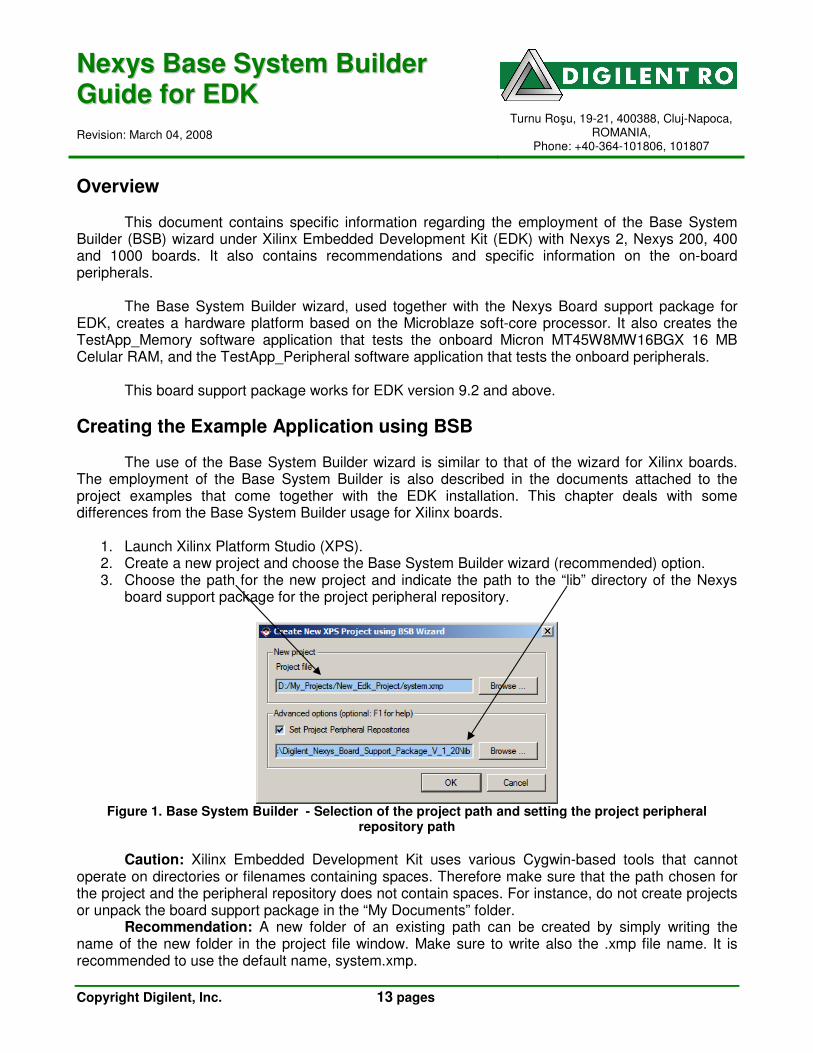
4. Choose “I would like to create a new design” in the next window. 5. In the “Base System Builder – Select Board” choose the proper board for your design.
a. Choose “I would like to create a system for the following development board” (default). b. Choose “Digilent” as vendor. c. Choose the appropriate board and revision.
Figure 2. Base System Builder - Select Board window
6. In the Base System Builder – Select Processor window, you can only choose Microblaze,
because the PowerPc processor is not supported by the FPGA devices available on the Nexys boards.
Nexys Base System Builder Guide for EDK Digilent RO
www.digilentinc.com Copyright Digilent, Inc. Page 3
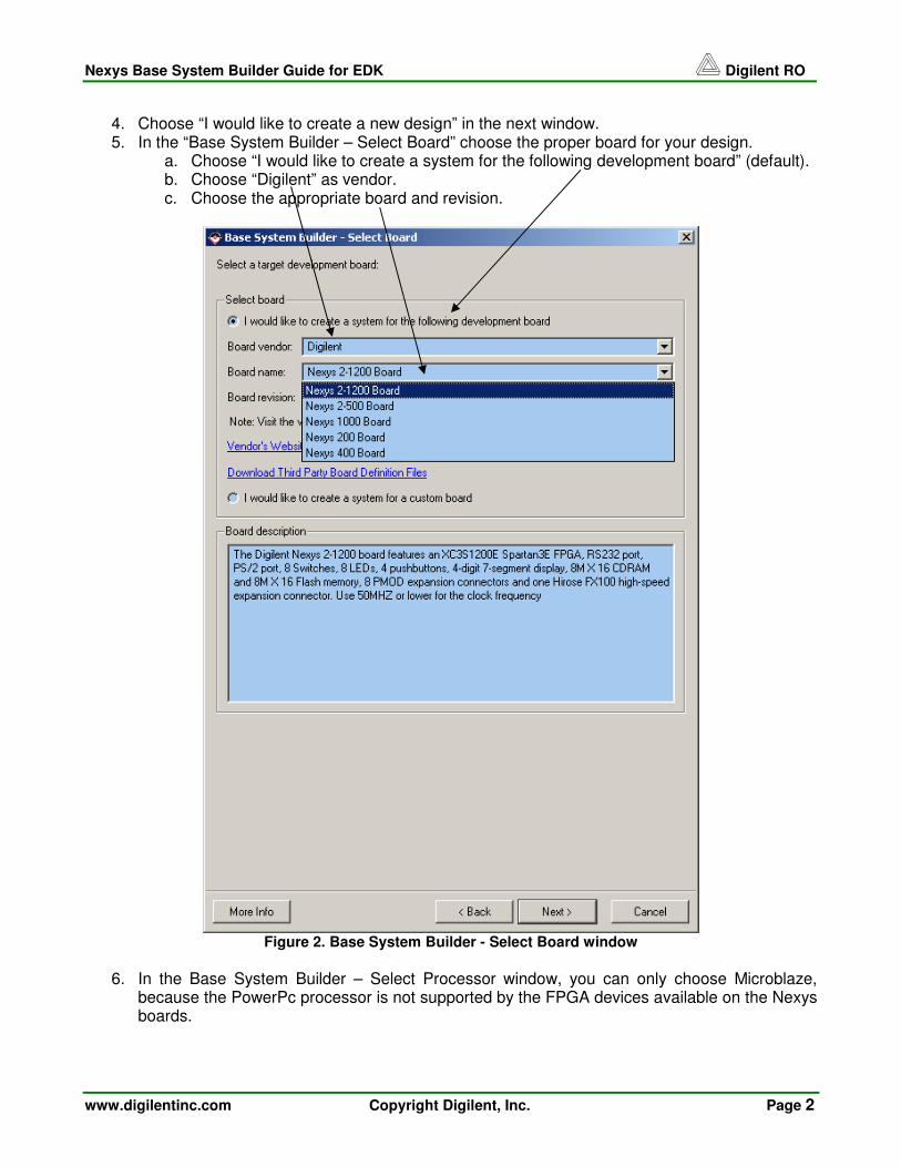
7. In the In the Base System Builder – Configure Microblaze Processor window, select the board
clock frequency, the processor - bus clock frequency and the size of the local memory (Block RAM).
a. For the Nexys 2 1200 and 1500 boards, the clock frequency is 50 MHz. The clock frequency on the Nexys 200, 400 and 1000 boards can be configured to either 25 Mhz, 50 Mhz or 100 Mhz. Use a clock frequency of 50Mhz or lower both for the reference clock frequency and the Processor-Bus clock frequency.
b. It is recommended to choose the On-Chip H/W debug module for the Debug I/F configuration.
c. If you want to run the TestApp_Peripheral software application from the Block RAM memory, choose 16KB for the Block RAM. If you choose a smaller memory, the TestApp_Peripheral application will not fit in the Block RAM and it would have to be run from the external memory using a debugger.
Figure 3. Base System Builder - Configure Microblaze Processor window
In the following BSB windows, the peripherals are chosen for the EDK project. There are some
particularities regarding the list of peripherals of the Nexys 200/400/1000 boards concerning the RS232 ports, which will be highlighted in the “Particularities of the Nexys 200/400/1000 boards I/O devices” chapter.
Nexys Base System Builder Guide for EDK Digilent RO
www.digilentinc.com Copyright Digilent, Inc. Page 4
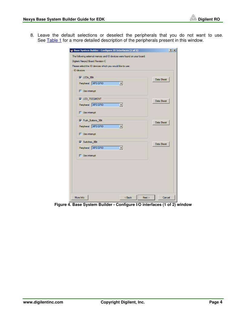
8. Leave the default selections or deselect the peripherals that you do not want to use.
See Table 1 for a more detailed description of the peripherals present in this window.
Figure 4. Base System Builder - Configure I/O interfaces (1 of 2) window
Nexys Base System Builder Guide for EDK Digilent RO
www.digilentinc.com Copyright Digilent, Inc. Page 5
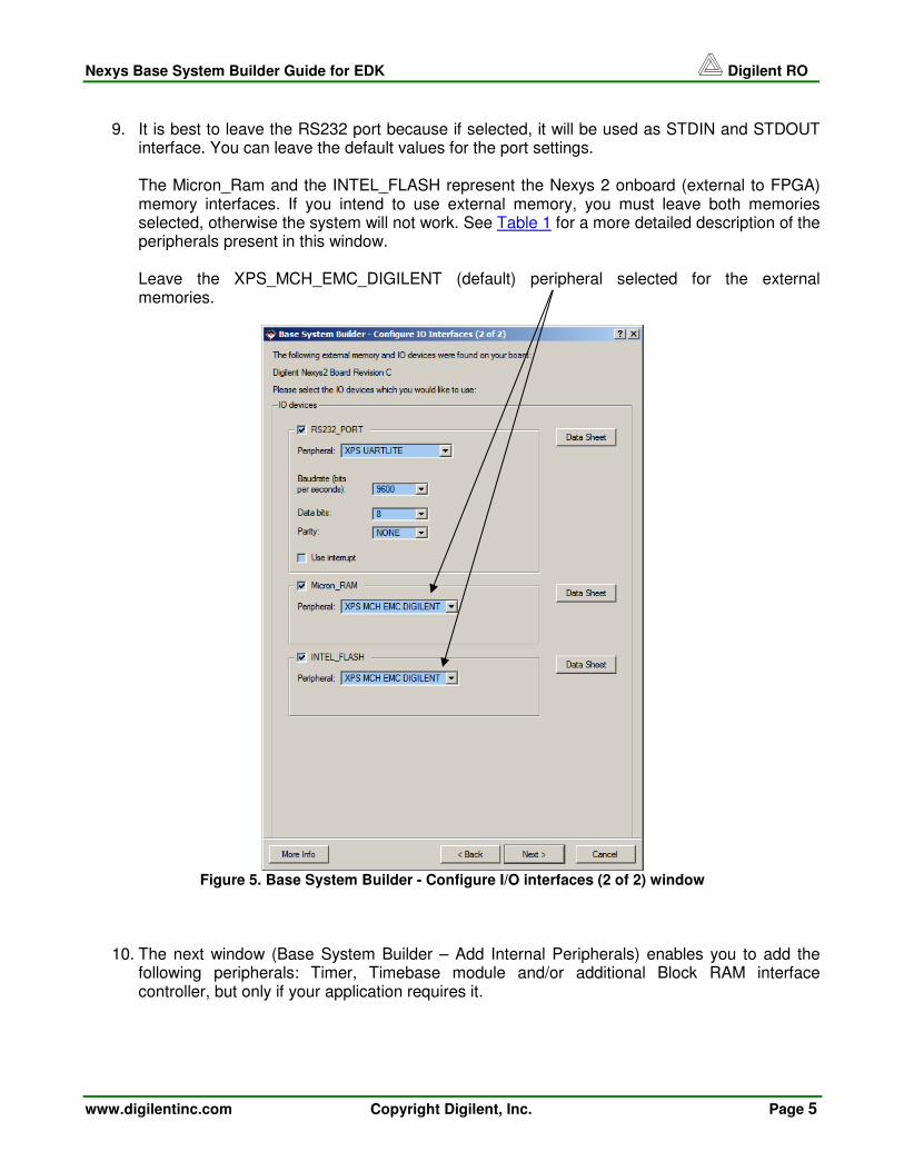
9. It is best to leave the RS232 port because if selected, it will be used as STDIN and STDOUT
interface. You can leave the default values for the port settings. The Micron_Ram and the INTEL_FLASH represent the Nexys 2 onboard (external to FPGA) memory interfaces. If you intend to use external memory, you must leave both memories selected, otherwise the system will not work. See Table 1 for a more detailed description of the peripherals present in this window. Leave the XPS_MCH_EMC_DIGILENT (default) peripheral selected for the external memories.
Figure 5. Base System Builder - Configure I/O interfaces (2 of 2) window
10. The next window (Base System Builder – Add Internal Peripherals) enables you to add the following peripherals: Timer, Timebase module and/or additional Block RAM interface controller, but only if your application requires it.
Nexys Base System Builder Guide for EDK Digilent RO
www.digilentinc.com Copyright Digilent, Inc. Page 6
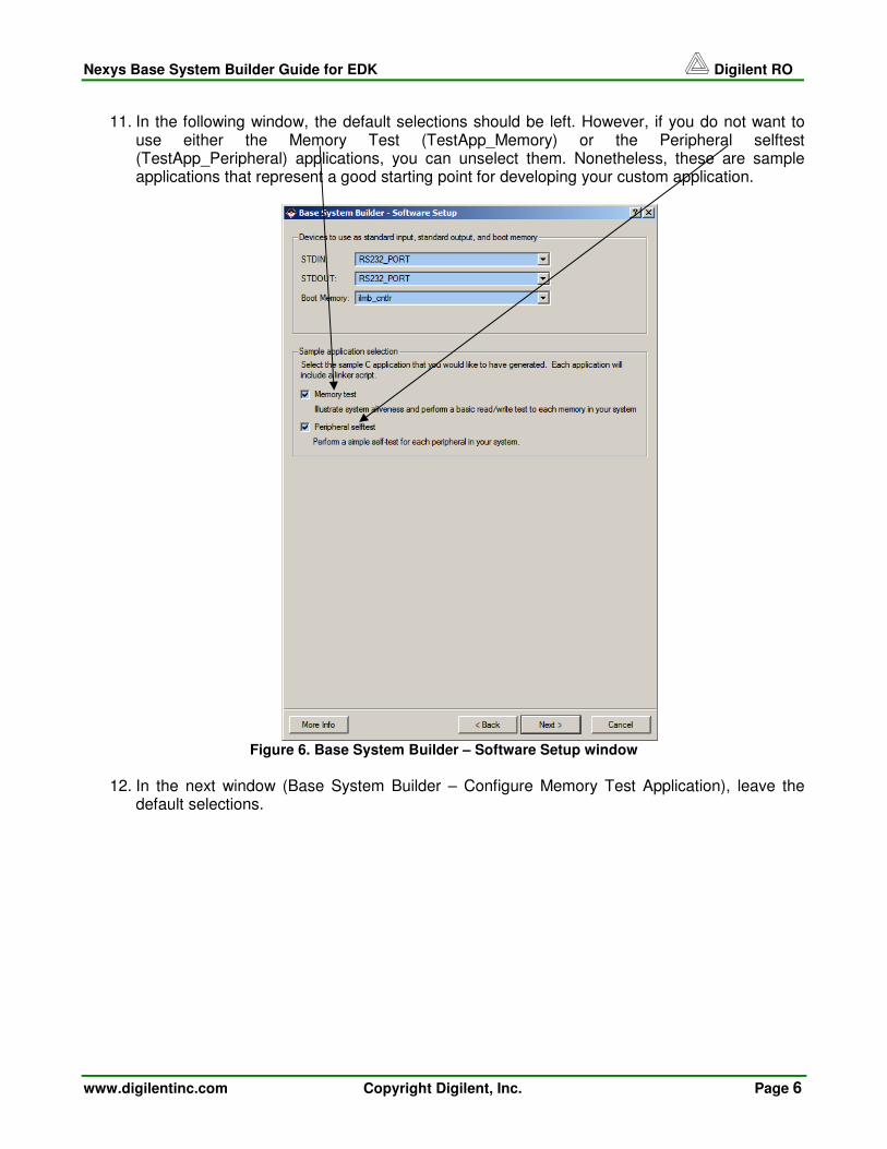
11. In the following window, the default selections should be left. However, if you do not want to
use either the Memory Test (TestApp_Memory) or the Peripheral selftest (TestApp_Peripheral) applications, you can unselect them. Nonetheless, these are sample applications that represent a good starting point for developing your custom application.
Figure 6. Base System Builder – Software Setup window
12. In the next window (Base System Builder – Configure Memory Test Application), leave the
default selections.
Nexys Base System Builder Guide for EDK Digilent RO
www.digilentinc.com Copyright Digilent, Inc. Page 7
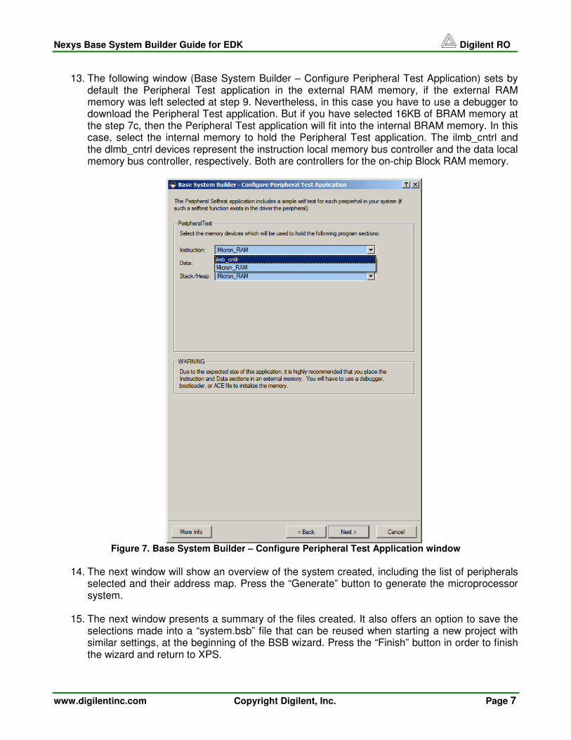
13. The following window (Base System Builder – Configure Peripheral Test Application) sets by
default the Peripheral Test application in the external RAM memory, if the external RAM memory was left selected at step 9. Nevertheless, in this case you have to use a debugger to download the Peripheral Test application. But if you have selected 16KB of BRAM memory at the step 7c, then the Peripheral Test application will fit into the internal BRAM memory. In this case, select the internal memory to hold the Peripheral Test application. The ilmb_cntrl and the dlmb_cntrl devices represent the instruction local memory bus controller and the data local memory bus controller, respectively. Both are controllers for the on-chip Block RAM memory.
Figure 7. Base System Builder – Configure Peripheral Test Application window
14. The next window will show an overview of the system created, including the list of peripherals
selected and their address map. Press the “Generate” button to generate the microprocessor system.
15. The next window presents a summary of the files created. It also offers an option to save the
selections made into a “system.bsb” file that can be reused when starting a new project with similar settings, at the beginning of the BSB wizard. Press the “Finish” button in order to finish the wizard and return to XPS.
Nexys Base System Builder Guide for EDK Digilent RO
www.digilentinc.com Copyright Digilent, Inc. Page 8
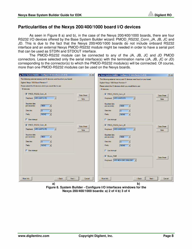
Particularities of the Nexys 200/400/1000 board I/O devices As seen in Figure 8 a) and b), in the case of the Nexys 200/400/1000 boards, there are four
RS232 I/O devices offered by the Base System Builder wizard: PMOD_RS232_Conn_JA, JB, JC and JD. This is due to the fact that the Nexys 200/400/1000 boards do not include onboard RS232 interface and an external Nexys PMOD-RS232 module might be needed in order to have a serial port that can be used as STDIN and STDOUT interface.
The PMOD-RS232 module can be connected to any of the JA, JB, JC and JD PMOD connectors. Leave selected only the serial interface(s) with the termination name (JA, JB, JC or JD) corresponding to the connector(s) to which the PMOD-RS232 module(s) will be connected. Of course, more than one PMOD-RS232 modules can be used on the Nexys boards.
a) b)
Figure 8. System Builder - Configure I/O interfaces windows for the Nexys 200/400/1000 boards: a) 2 of 4 b) 3 of 4
Nexys Base System Builder Guide for EDK Digilent RO
www.digilentinc.com Copyright Digilent, Inc. Page 9
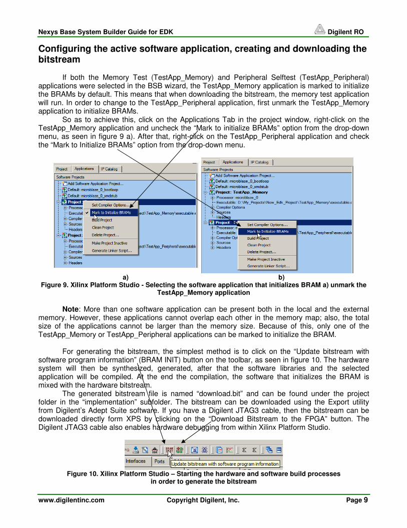
Configuring the active software application, creating and downloading the bitstream If both the Memory Test (TestApp_Memory) and Peripheral Selftest (TestApp_Peripheral) applications were selected in the BSB wizard, the TestApp_Memory application is marked to initialize the BRAMs by default. This means that when downloading the bitstream, the memory test application will run. In order to change to the TestApp_Peripheral application, first unmark the TestApp_Memory application to initialize BRAMs.
So as to achieve this, click on the Applications Tab in the project window, right-click on the TestApp_Memory application and uncheck the “Mark to initialize BRAMs” option from the drop-down menu, as seen in figure 9 a). After that, right-click on the TestApp_Peripheral application and check the “Mark to Initialize BRAMs” option from the drop-down menu.
a) b)
Figure 9. Xilinx Platform Studio - Selecting the software application that initializes BRAM a) unmark the TestApp_Memory application
Note: More than one software application can be present both in the local and the external
memory. However, these applications cannot overlap each other in the memory map; also, the total size of the applications cannot be larger than the memory size. Because of this, only one of the TestApp_Memory or TestApp_Peripheral applications can be marked to initialize the BRAM. For generating the bitstream, the simplest method is to click on the “Update bitstream with software program information” (BRAM INIT) button on the toolbar, as seen in figure 10. The hardware system will then be synthesized, generated, after that the software libraries and the selected application will be compiled. At the end the compilation, the software that initializes the BRAM is mixed with the hardware bitstream. The generated bitstream file is named “download.bit” and can be found under the project folder in the “implementation” subfolder. The bitstream can be downloaded using the Export utility from Digilent’s Adept Suite software. If you have a Digilent JTAG3 cable, then the bitstream can be downloaded directly form XPS by clicking on the “Download Bitstream to the FPGA” button. The Digilent JTAG3 cable also enables hardware debugging from within Xilinx Platform Studio.
Figure 10. Xilinx Platform Studio – Starting the hardware and software build processes
in order to generate the bitstream
Nexys Base System Builder Guide for EDK Digilent RO
www.digilentinc.com Copyright Digilent, Inc. Page 10
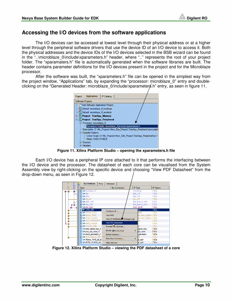
Accessing the I/O devices from the software applications The I/O devices can be accessed at lowest level through their physical address or at a higher level through the peripheral software drivers that use the device ID of an I/O device to access it. Both the physical addresses and the device IDs of the I/O devices selected in the BSB wizard can be found in the “..\microblaze_0\include\xparameters.h” header, where “..” represents the root of your project folder. The “xparamaters.h” file is automatically generated when the software libraries are built. The header contains parameter definitions for the I/O devices present in the project and for the Microblaze processor.
After the software was built, the “xparameters.h” file can be opened in the simplest way from the project window, “Applications” tab, by expanding the “processor: microblaze_0” entry and double-clicking on the “Generated Header: microblaze_0/include/xparameters.h” entry, as seen in figure 11.
Figure 11. Xilinx Platform Studio – opening the xparameters.h file
Each I/O device has a peripheral IP core attached to it that performs the interfacing between the I/O device and the processor. The datasheet of each core can be visualised from the System Assembly view by right-clicking on the specific device and choosing “View PDF Datasheet” from the drop-down menu, as seen in Figure 12.
Figure 12. Xilinx Platform Studio – viewing the PDF datasheet of a core
Nexys Base System Builder Guide for EDK Digilent RO
www.digilentinc.com Copyright Digilent, Inc. Page 11
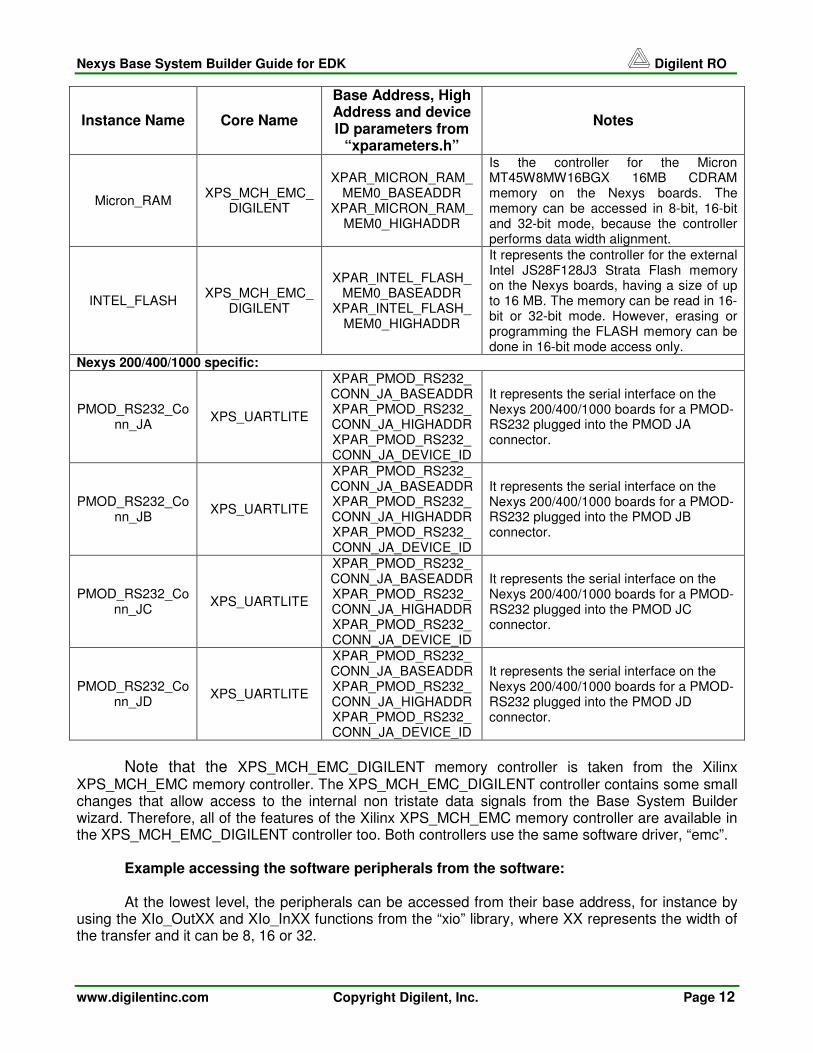
Table 1 below presents the instance names, core names, base address, high address and device ID parameters for the I/O devices on the Nexys2 – 500, 1200 and Nexys 200/400/1000 boards. Table 1. List of I/O devices on the Nexys boards
Instance Name Core Name
Base Address, High Address and device ID
parameters from “xparameters.h”
Notes
LEDS_8Bit XPS_GPIO
XPAR_LEDS_8BIT
_BASEADDR XPAR_LEDS_8BIT
_HIGHADDR XPAR_LEDS_8BIT
_DEVICE_ID
The I/O interface represents the eight LEDs on the Nexys boards. The least significant byte of the data sent to the I/O device is the LED data (1 to turn on, 0 to turn off)
LED_7SEGMENT XPS_GPIO
XPAR_LED_7SEGMENT_BASEADD
R XPAR_LED_7SEGMENT_HIGHADDR XPAR_LED_7SEGMENT_DEVICE_ID
The I/O interface represents the four-digit seven-segment display on the Nexys board. From the data sent to the I/O interface, only the least significant 12 bits are valid data: Bits 11 downto 8 correspond to the common anodes on the four digits: bit 11 – AN0, bit 10 – AN1, bit 9 – AN2, bit 8 – AN3, bit 7 represents the decimal point and bits 6 downto 0 correspond to the cathode G downto A segments. Note that both the cathode and anode data is active – low (0 when turned on)
Push_Buttons_3Bit XPS_GPIO
XPAR_PUSH_BUTTONS_3BIT_BASE
ADDR XPAR_PUSH_BUTTONS_3BIT_HIGH
ADDR XPAR_PUSH_BUTTONS_3BIT_DEVI
CE_ID
The I/O interface corresponds to the three pushbuttons from the Nexys board. The three least significant bits of the data read from the interface symbolize the state of the pushbuttons (1 – pressed, 0 – released): Bit 2 – BTN3, Bit1 – BTN2, BIT0 – BTN1 Note that by default BTN0 is used as system reset. Writing to the I/O interface has no effect.
Switches_8Bit XPS_GPIO
XPAR_SWITCHES_8BIT_BASEADDR XPAR_SWITCHES_8BIT_HIGHADDR XPAR_SWITCHES_8BIT_DEVICE_ID
The I/O interface represents the eight switches on the Nexys board. The eight least significant bits of the data read from the interface correspond to the switch data (1 if turned on, 0 if turned off) Writing to the I/O interface has no effect.
RS232_PORT XPS_UARTLITE
XPAR_RS232_PORT_BASEADDR
XPAR_RS232_PORT_HIGHADDR
XPAR_RS232_PORT_DEVICE_ID
It represents the serial interface of the Nexys 2 board. By default, this port is used as STDIN and STDOUT interface. .
Table 1. List of I/O devices on the Nexys boards (continued)
Nexys Base System Builder Guide for EDK Digilent RO
www.digilentinc.com Copyright Digilent, Inc. Page 12
Instance Name Core Name
Base Address, High Address and device ID parameters from
“xparameters.h”
Notes
Micron_RAM XPS_MCH_EMC_
DIGILENT
XPAR_MICRON_RAM_
MEM0_BASEADDR XPAR_MICRON_RAM_
MEM0_HIGHADDR
Is the controller for the Micron MT45W8MW16BGX 16MB CDRAM memory on the Nexys boards. The memory can be accessed in 8-bit, 16-bit and 32-bit mode, because the controller performs data width alignment.
INTEL_FLASH XPS_MCH_EMC_
DIGILENT
XPAR_INTEL_FLASH_
MEM0_BASEADDR XPAR_INTEL_FLASH_
MEM0_HIGHADDR
It represents the controller for the external Intel JS28F128J3 Strata Flash memory on the Nexys boards, having a size of up to 16 MB. The memory can be read in 16-bit or 32-bit mode. However, erasing or programming the FLASH memory can be done in 16-bit mode access only.
Nexys 200/400/1000 specific:
PMOD_RS232_Conn_JA
XPS_UARTLITE
XPAR_PMOD_RS232_CONN_JA_BASEADDR XPAR_PMOD_RS232_CONN_JA_HIGHADDR XPAR_PMOD_RS232_CONN_JA_DEVICE_ID
It represents the serial interface on the Nexys 200/400/1000 boards for a PMOD-RS232 plugged into the PMOD JA connector.
PMOD_RS232_Conn_JB
XPS_UARTLITE
XPAR_PMOD_RS232_CONN_JA_BASEADDR XPAR_PMOD_RS232_CONN_JA_HIGHADDR XPAR_PMOD_RS232_CONN_JA_DEVICE_ID
It represents the serial interface on the Nexys 200/400/1000 boards for a PMOD-RS232 plugged into the PMOD JB connector.
PMOD_RS232_Conn_JC
XPS_UARTLITE
XPAR_PMOD_RS232_CONN_JA_BASEADDR XPAR_PMOD_RS232_CONN_JA_HIGHADDR XPAR_PMOD_RS232_CONN_JA_DEVICE_ID
It represents the serial interface on the Nexys 200/400/1000 boards for a PMOD-RS232 plugged into the PMOD JC connector.
PMOD_RS232_Conn_JD
XPS_UARTLITE
XPAR_PMOD_RS232_CONN_JA_BASEADDR XPAR_PMOD_RS232_CONN_JA_HIGHADDR XPAR_PMOD_RS232_CONN_JA_DEVICE_ID
It represents the serial interface on the Nexys 200/400/1000 boards for a PMOD-RS232 plugged into the PMOD JD connector.
Note that the XPS_MCH_EMC_DIGILENT memory controller is taken from the Xilinx XPS_MCH_EMC memory controller. The XPS_MCH_EMC_DIGILENT controller contains some small changes that allow access to the internal non tristate data signals from the Base System Builder wizard. Therefore, all of the features of the Xilinx XPS_MCH_EMC memory controller are available in the XPS_MCH_EMC_DIGILENT controller too. Both controllers use the same software driver, “emc”. Example accessing the software peripherals from the software:
At the lowest level, the peripherals can be accessed from their base address, for instance by using the XIo_OutXX and XIo_InXX functions from the “xio” library, where XX represents the width of the transfer and it can be 8, 16 or 32.
Nexys Base System Builder Guide for EDK Digilent RO
www.digilentinc.com Copyright Digilent, Inc. Page 13
For example, to turn on Leds 6, 4, 2, 1 and 0 on the Nexys board and to read the switch data: //in the inclusion section: #include “xio.h” … //in the main section: Xuint32 Switch_Data; … XIo_Out32(XPAR_LEDS_8BIT_BASEADDR, 0x57); Switch_Data = XIo_In32 (XPAR_SWITCHES_8BIT_BASEADDR);
Because the Microblaze is a 32-bit processor, generally all of the I/O devices should be accessed in 32-bit mode unless there is no need for 16-bit or 8-bit access. For instance, the Intel Flash memory has to be accessed in 16-bit mode when erasing or programming. Note that the XPS_GPIO devices have to be accessed in 32-bit mode.
Revision History 1_22: Added support for Nexys 2 – 1200 board, rev. C 1_20:
The board support package is compatible with EDK version 9.2 and above. In order to access the Nexys onboard memories, the Nexys_EMC OPB bus compliant memory controller was replaced by a modified version of the PLBv4.6 bus compliant XPS_MCH_EMC memory controller, namely XPS_MCH_EMC_DIGILENT Created the Nexys Base System Builder Guide for EDK document
1_01:
Added support for Nexys 2 board, rev. A 1_00:
Release version