Embed Size (px)
Citation preview

Andes Instruction SetAndes Instruction Set
2
AgendaAgenda
Andes Instruction Set Architecture Introduction32-bit Baseline Instructions16-bit Baseline InstructionsExtension Instructions
Andes System Privileged ArchitectureMemory Management UnitInterruption ArchitecturePerformance Monitoring MechanismLocal Memory InterfaceHigh Speed Memory Port SupportSystem Registers
back
3
AgendaAgenda
Andes Instruction Set Architecture Introduction32-bit Baseline Instructions16-bit Baseline InstructionsExtension Instructions
Andes System Privileged ArchitectureMemory Management UnitInterruption ArchitecturePerformance Monitoring MechanismLocal Memory InterfaceHigh Speed Memory Port SupportSystem Registers
back
4
ISA FeaturesISA Features
32/16-bit mixed-length RISC ISA16-bit is a frequently used subset.32/16-bit can be mixed in a program.No 32/16-bit mode switching is required.
EndianInstruction: big-endian formatData: mixed-endian format
PrivilegeUser / Super-user.
Instruction LengthBit [31] of a 32-bit instruction and Bit [15] of a 16-bit instruction are used to determine instruction length.
0
1 1
1
0
0
1
5
ISA FeaturesISA Features
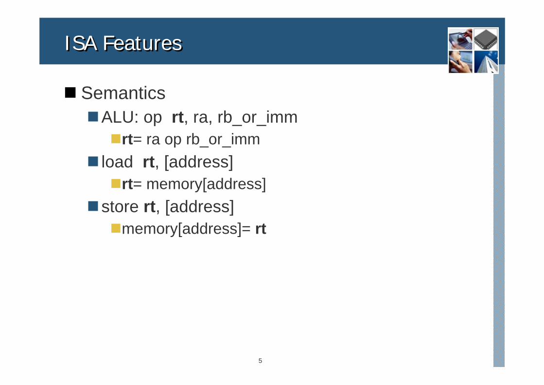
SemanticsALU: op rt, ra, rb_or_imm
rt= ra op rb_or_immload rt, [address]
rt= memory[address]store rt, [address]
memory[address]= rt
6
Data TypesData Types
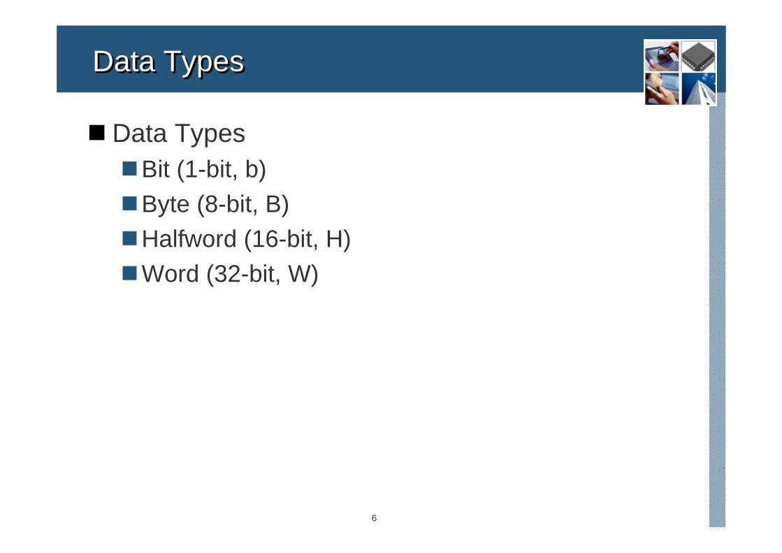
Data TypesBit (1-bit, b)Byte (8-bit, B)Halfword (16-bit, H)Word (32-bit, W)
7
General Purpose RegistersGeneral Purpose Registers
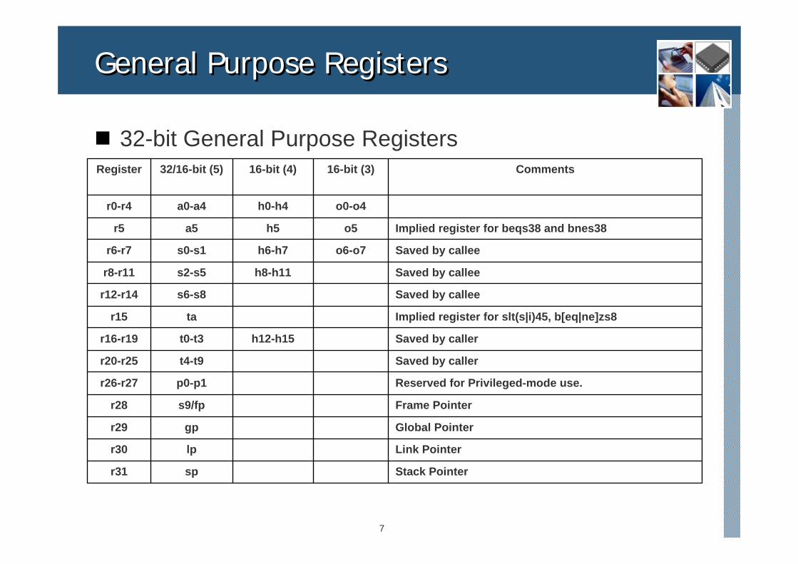
32-bit General Purpose Registers
Stack Pointerspr31
Link Pointerlpr30
Global Pointergpr29
Frame Pointers9/fpr28
Reserved for Privileged-mode use.p0-p1r26-r27
Saved by callert4-t9r20-r25
Saved by callerh12-h15t0-t3r16-r19
Implied register for slt(s|i)45, b[eq|ne]zs8tar15
Saved by callees6-s8r12-r14
Saved by calleeh8-h11s2-s5r8-r11
Saved by calleeo6-o7h6-h7s0-s1r6-r7
Implied register for beqs38 and bnes38o5h5a5r5
o0-o4h0-h4a0-a4r0-r4
Comments16-bit (3)16-bit (4)32/16-bit (5)Register
8
General Purpose Registers - ReducedGeneral Purpose Registers - Reduced
16/32-bit General Purpose Registers
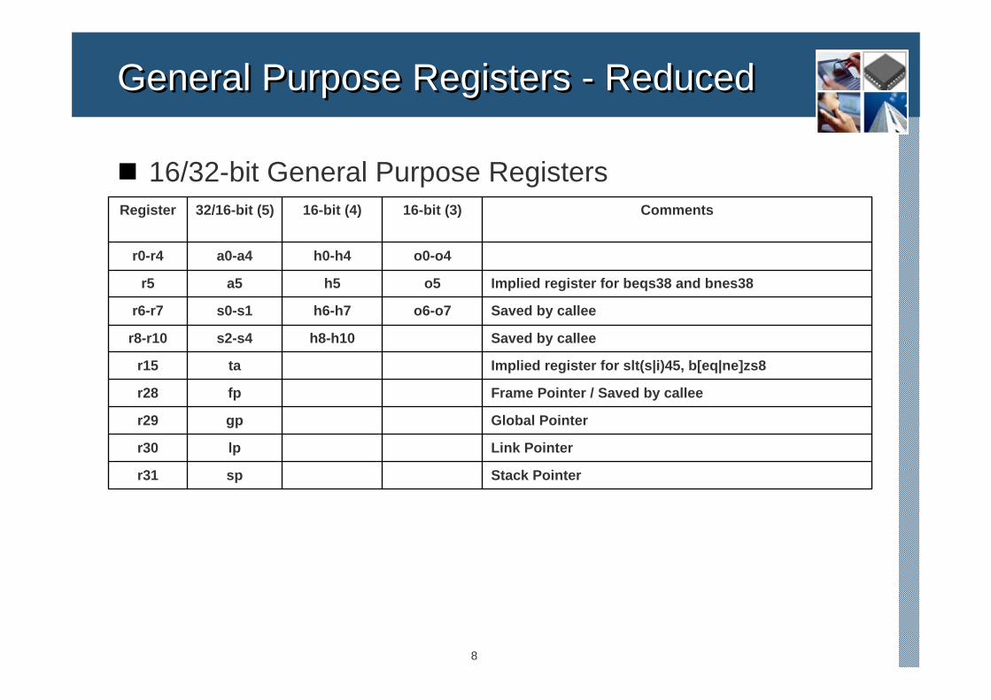
Stack Pointerspr31
Link Pointerlpr30
Global Pointergpr29
Frame Pointer / Saved by calleefpr28
Implied register for slt(s|i)45, b[eq|ne]zs8tar15
Saved by calleeh8-h10s2-s4r8-r10
Saved by calleeo6-o7h6-h7s0-s1r6-r7
Implied register for beqs38 and bnes38o5h5a5r5
o0-o4h0-h4a0-a4r0-r4
Comments16-bit (3)16-bit (4)32/16-bit (5)Register
9
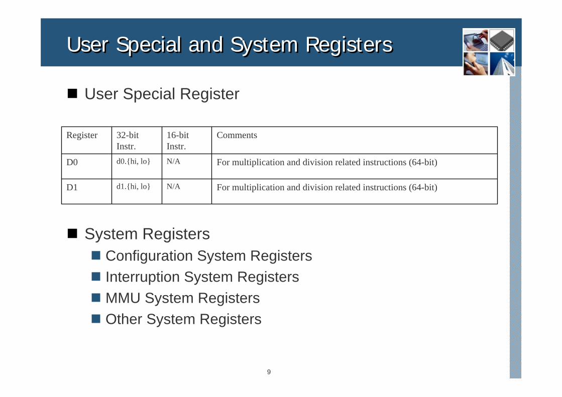
User Special and System RegistersUser Special and System Registers
For multiplication and division related instructions (64-bit)N/Ad1.{hi, lo}D1
For multiplication and division related instructions (64-bit)N/Ad0.{hi, lo}D0
Comments16-bit Instr.
32-bit Instr.
Register
User Special Register
System RegistersConfiguration System RegistersInterruption System RegistersMMU System RegistersOther System Registers
10
AgendaAgenda
Andes Instruction Set Architecture Introduction32-bit Baseline Instructions16-bit Baseline InstructionsExtension Instructions
Andes System Privileged ArchitectureMemory Management UnitInterruption ArchitecturePerformance Monitoring MechanismLocal Memory InterfaceHigh Speed Memory Port SupportSystem Registers
back
11
32-bit Baseline Instruction32-bit Baseline Instruction
The minimum set of Andes ISA.A complete set of instructions which can be used to construct a fully-functional Andes system or program.
Instruction CatalogData ProcessingLoad and StoreFlow Control (Jump and Branch)Privileged Resource AccessMiscellaneous
12
32-bit Baseline – data processing 32-bit Baseline – data processing
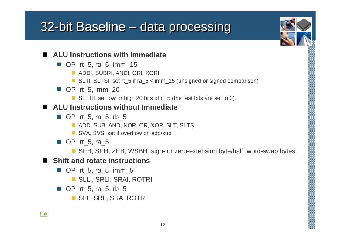
ALU Instructions with ImmediateOP rt_5, ra_5, imm_15
ADDI, SUBRI, ANDI, ORI, XORISLTI, SLTSI: set rt_5 if ra_5 < imm_15 (unsigned or signed comparison)
OP rt_5, imm_20SETHI: set low or high 20 bits of rt_5 (the rest bits are set to 0).
ALU Instructions without ImmediateOP rt_5, ra_5, rb_5
ADD, SUB, AND, NOR, OR, XOR, SLT, SLTSSVA, SVS: set if overflow on add/sub
OP rt_5, ra_5SEB, SEH, ZEB, WSBH: sign- or zero-extension byte/half, word-swap bytes.
Shift and rotate instructionsOP rt_5, ra_5, imm_5
SLLI, SRLI, SRAI, ROTRIOP rt_5, ra_5, rb_5
SLL, SRL, SRA, ROTR
link
13
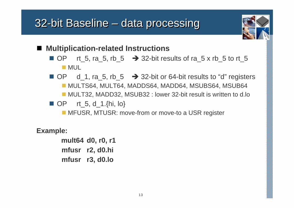
32-bit Baseline – data processing 32-bit Baseline – data processing
Multiplication-related Instructions OP rt_5, ra_5, rb_5 32-bit results of ra_5 x rb_5 to rt_5
MULOP d_1, ra_5, rb_5 32-bit or 64-bit results to “d” registers
MULTS64, MULT64, MADDS64, MADD64, MSUBS64, MSUB64MULT32, MADD32, MSUB32 : lower 32-bit result is written to d.lo
OP rt_5, d_1.{hi, lo} MFUSR, MTUSR: move-from or move-to a USR register
Example:mult64 d0, r0, r1mfusr r2, d0.himfusr r3, d0.lo
14
32-bit Baseline – load / store32-bit Baseline – load / store
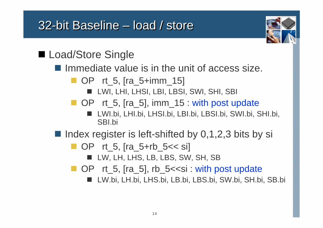
Load/Store SingleImmediate value is in the unit of access size.
OP rt_5, [ra_5+imm_15]LWI, LHI, LHSI, LBI, LBSI, SWI, SHI, SBI
OP rt_5, [ra_5], imm_15 : with post updateLWI.bi, LHI.bi, LHSI.bi, LBI.bi, LBSI.bi, SWI.bi, SHI.bi, SBI.bi
Index register is left-shifted by 0,1,2,3 bits by siOP rt_5, [ra_5+rb_5<< si]
LW, LH, LHS, LB, LBS, SW, SH, SBOP rt_5, [ra_5], rb_5<<si : with post update
LW.bi, LH.bi, LHS.bi, LB.bi, LBS.bi, SW.bi, SH.bi, SB.bi
15
32-bit Baseline – load / store32-bit Baseline – load / store
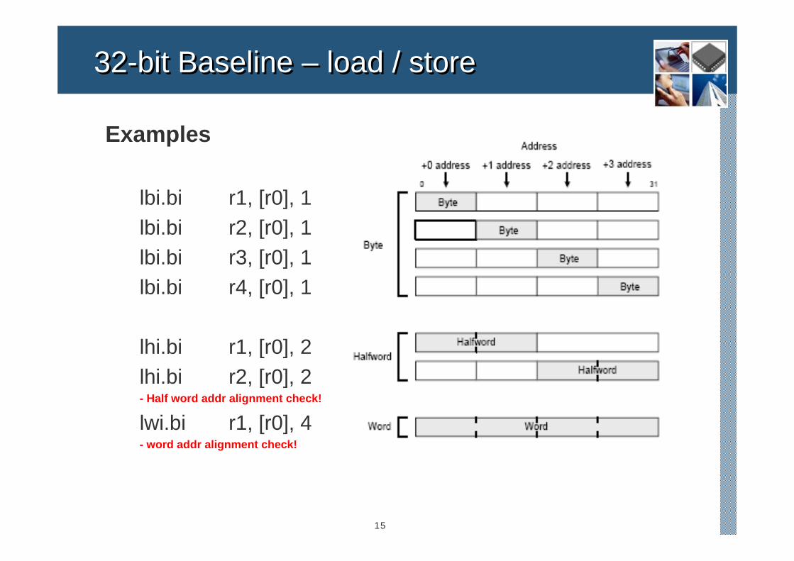
Examples
lbi.bi r1, [r0], 1lbi.bi r2, [r0], 1lbi.bi r3, [r0], 1lbi.bi r4, [r0], 1
lhi.bi r1, [r0], 2lhi.bi r2, [r0], 2- Half word addr alignment check!
lwi.bi r1, [r0], 4- word addr alignment check!
16
32-bit Baseline – load / store32-bit Baseline – load / store
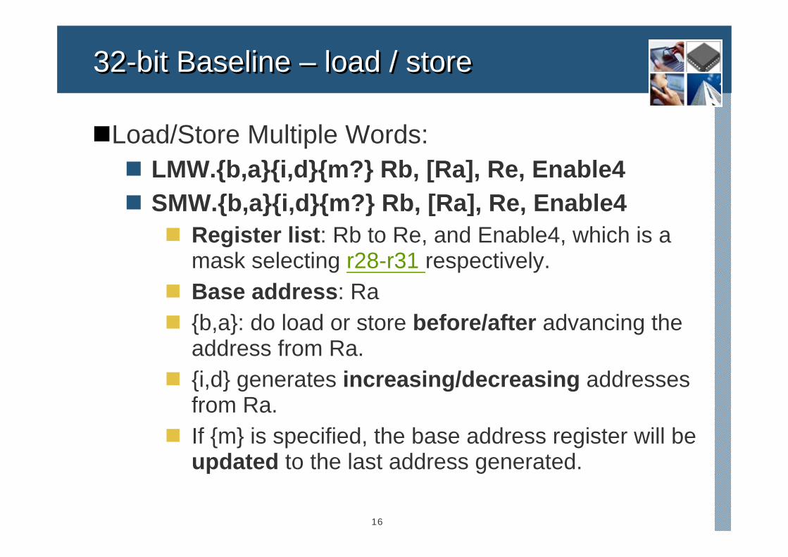
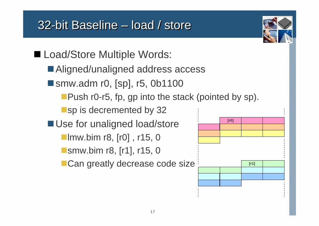
Load/Store Multiple Words:LMW.{b,a}{i,d}{m?} Rb, [Ra], Re, Enable4SMW.{b,a}{i,d}{m?} Rb, [Ra], Re, Enable4
Register list: Rb to Re, and Enable4, which is a mask selecting r28-r31 respectively.Base address: Ra{b,a}: do load or store before/after advancing the address from Ra.{i,d} generates increasing/decreasing addresses from Ra.If {m} is specified, the base address register will be updated to the last address generated.
17
Load/Store Multiple Words:Aligned/unaligned address accesssmw.adm r0, [sp], r5, 0b1100
Push r0-r5, fp, gp into the stack (pointed by sp).sp is decremented by 32
Use for unaligned load/storelmw.bim r8, [r0] , r15, 0smw.bim r8, [r1], r15, 0Can greatly decrease code size
32-bit Baseline – load / store32-bit Baseline – load / store
[r0]
[r1]
18
32-bit Baseline – flow control32-bit Baseline – flow control
Jump InstructionOP imm_24
J: unconditional direct branchJAL: direct function call
OP rb_5 JR: unconditional indirect branchRET: returnJRAL: indirect function call
Branch Instruction OP rt_5, ra_5, imm_14
BEQ, BNEOP rt_5, imm_16
BEQZ, BNEZ, BGEZ, BLTZ, BGTZ, BLEZlink
19
32-bit Baseline – privilege32-bit Baseline – privilege
Privileged Resource AccessSystem and Special Register
MFSR/MTSR, MFUSR/MTUSRSETEND, SETGIEJRAL.xTON, JR.xTOFF, RET.xTOFF
Cache ManagementCCTL
TLB ManagementTLBOP
tlbop $r0,TargetRead
link
20
32-bit Baseline – miscellaneous32-bit Baseline – miscellaneous
MiscellaneousData Prefetch : DPREF, DPREFI.Interruption : BREAK, SYSCALL, TRAP,
TEQZ, TNEZ, IRET.Serialization : ISB, DSB.Synchronization : ISYNC, MSYNC.Standby : STANDBY.No Operation : NOP.
link
21
AgendaAgenda
Andes Instruction Set Architecture Introduction32-bit Baseline Instructions16-bit Baseline InstructionsExtension Instructions
Andes System Privileged ArchitectureMemory Management UnitInterruption ArchitecturePerformance Monitoring MechanismLocal Memory InterfaceHigh Speed Memory Port SupportSystem Registers
back
22
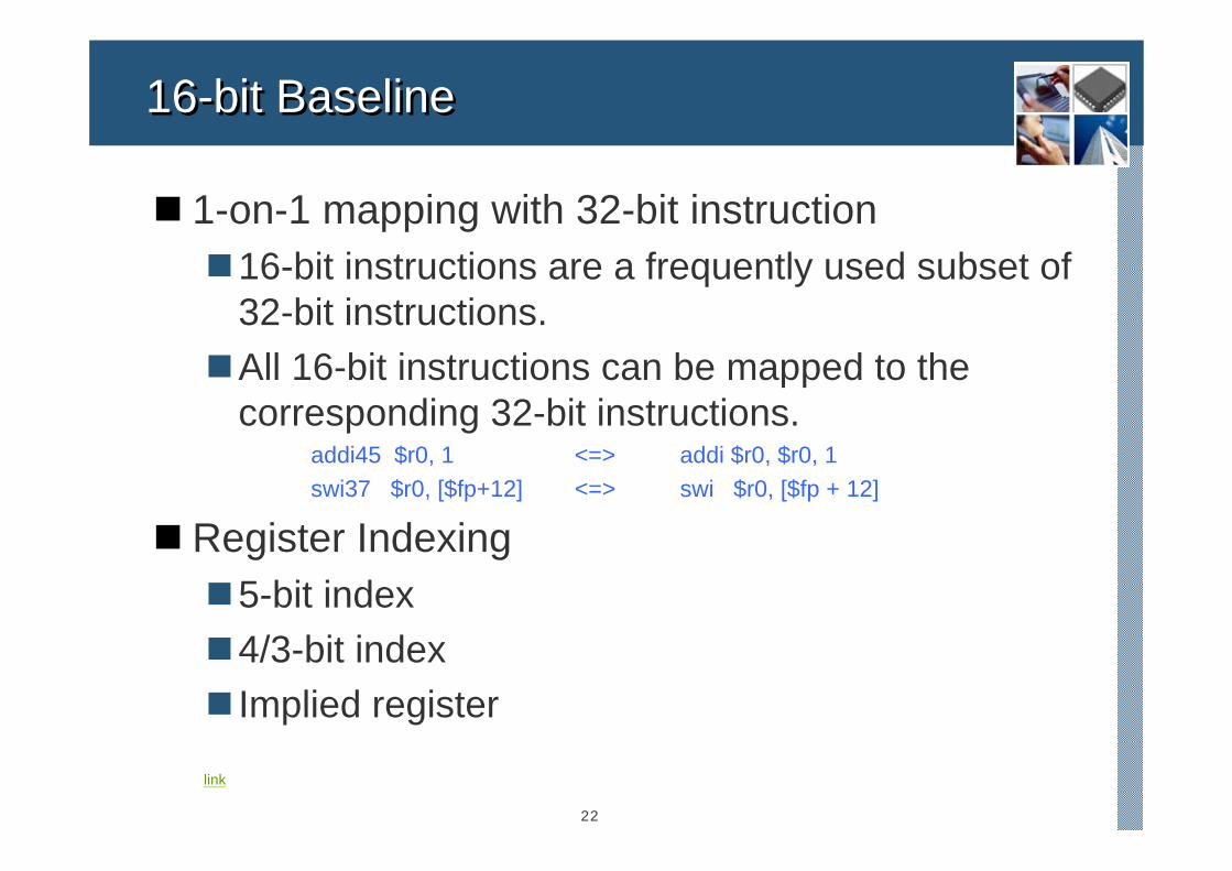
16-bit Baseline16-bit Baseline
1-on-1 mapping with 32-bit instruction16-bit instructions are a frequently used subset of 32-bit instructions.All 16-bit instructions can be mapped to the corresponding 32-bit instructions.
addi45 $r0, 1 <=> addi $r0, $r0, 1swi37 $r0, [$fp+12] <=> swi $r0, [$fp + 12]
Register Indexing5-bit index4/3-bit indexImplied register
link
23
16-bit Baseline16-bit Baseline
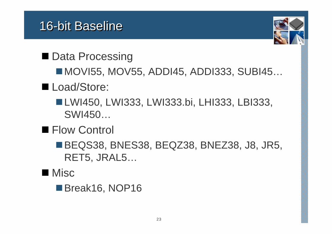
Data ProcessingMOVI55, MOV55, ADDI45, ADDI333, SUBI45…
Load/Store:LWI450, LWI333, LWI333.bi, LHI333, LBI333, SWI450…
Flow ControlBEQS38, BNES38, BEQZ38, BNEZ38, J8, JR5, RET5, JRAL5…
MiscBreak16, NOP16
24
AgendaAgenda
Andes Instruction Set Architecture Introduction32-bit Baseline Instructions16-bit Baseline InstructionsExtension Instructions
Andes System Privileged ArchitectureMemory Management UnitInterruption ArchitecturePerformance Monitoring MechanismLocal Memory InterfaceHigh Speed Memory Port SupportSystem Registers
back
25
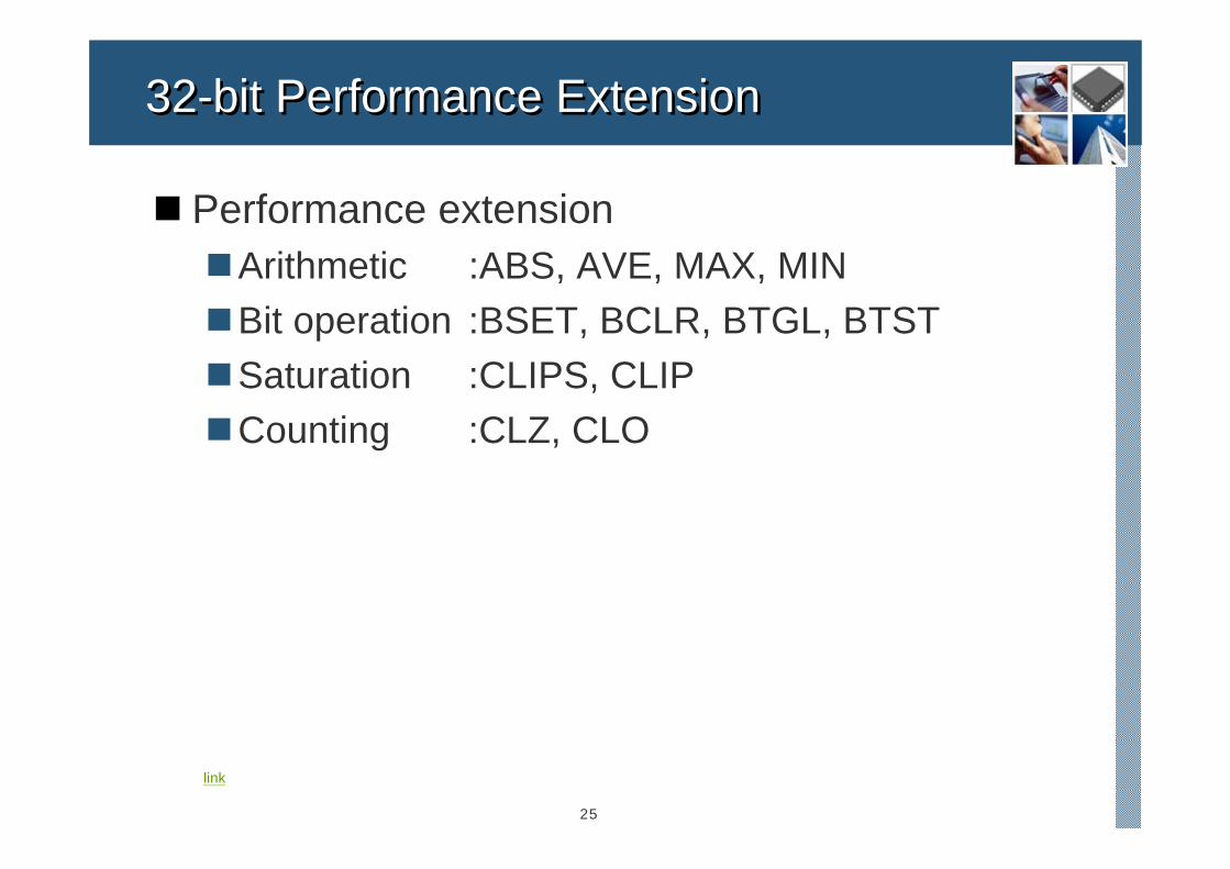
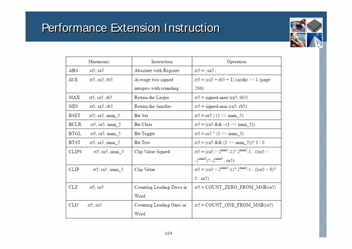
32-bit Performance Extension32-bit Performance Extension
Performance extensionArithmetic :ABS, AVE, MAX, MINBit operation :BSET, BCLR, BTGL, BTSTSaturation :CLIPS, CLIPCounting :CLZ, CLO
link
26
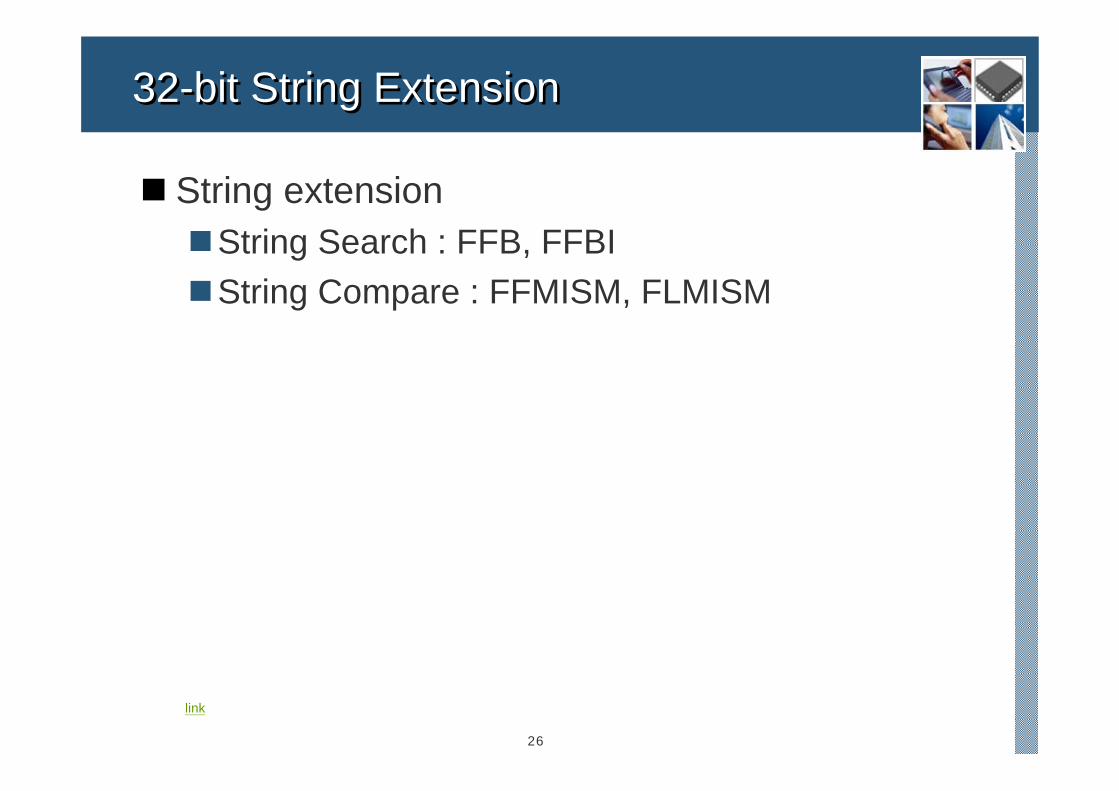
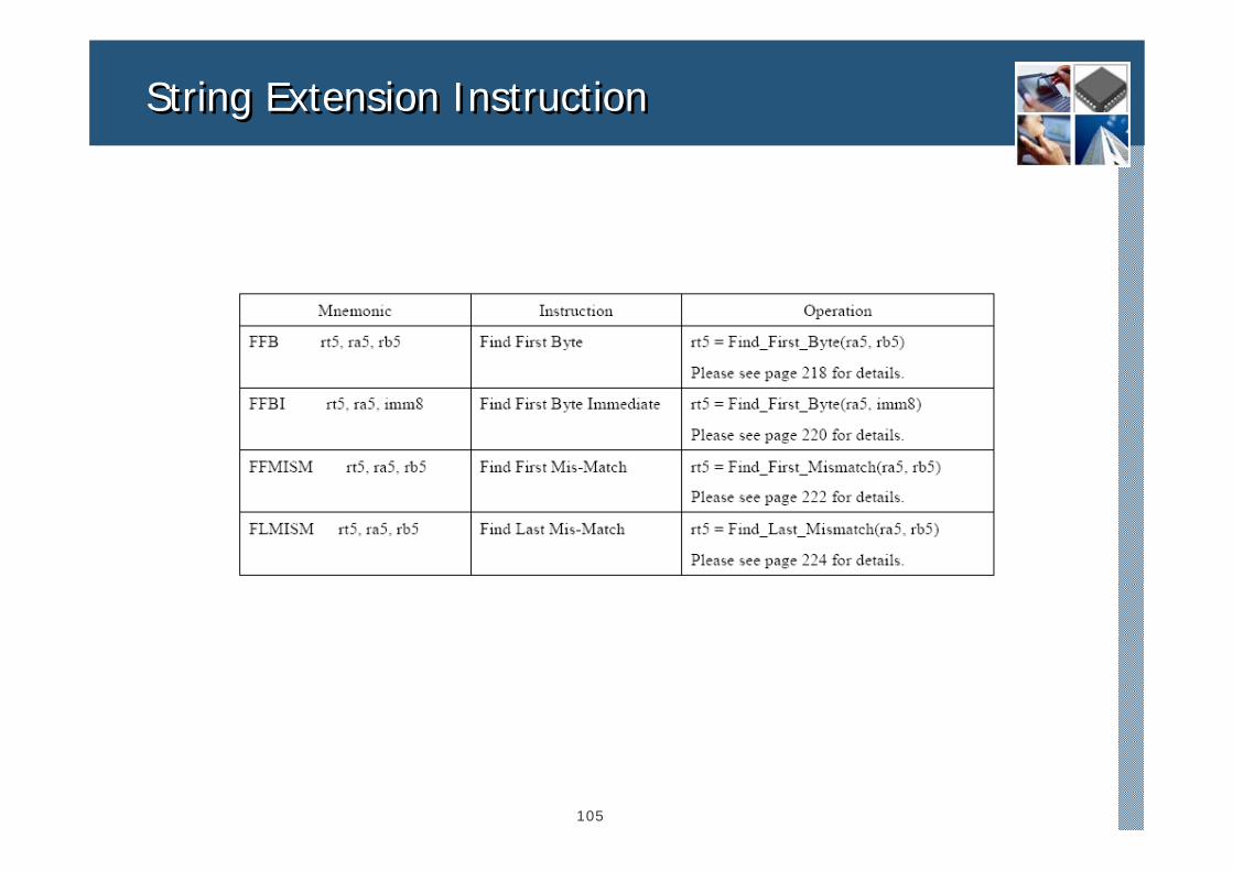
32-bit String Extension32-bit String Extension
String extensionString Search : FFB, FFBIString Compare : FFMISM, FLMISM
link
27
AgendaAgenda
Andes Instruction Set Architecture Introduction32-bit Baseline Instructions16-bit Baseline InstructionsExtension Instructions
Andes System Privileged ArchitectureMemory Management UnitInterruption ArchitecturePerformance Monitoring MechanismLocal Memory InterfaceHigh Speed Memory Port SupportSystem Registers
back
28
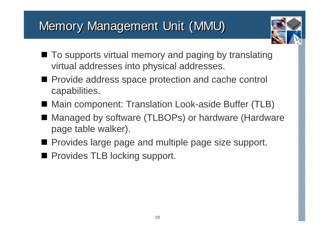
Memory Management Unit (MMU)Memory Management Unit (MMU)
To supports virtual memory and paging by translating virtual addresses into physical addresses.Provide address space protection and cache control capabilities.Main component: Translation Look-aside Buffer (TLB)Managed by software (TLBOPs) or hardware (Hardware page table walker).Provides large page and multiple page size support.Provides TLB locking support.
29
Memory Management Unit (MMU)Memory Management Unit (MMU)
Virtual Address (VA): virtual/logical address space. 32-bit wide, thus 4 GB space.Physical Address (PA): The real address used to access system bus. Typically, managed by superuser mode processes.When VA->PA translation process is disabled, VA is equivalent to PA.
30
Address space attributesAddress space attributes
For access control, and sharing of program or data.Defines various properties
Cachebility requirement/hintAccess/execute permissions
Translated: defined in Page Table Entry.Non-translated: defined in system register, selected by PA index.
31
Hardware Page Table WalkerHardware Page Table Walker
Responsible for reading TLB entry located in system memory under Main TLB miss condition. Less flexible than software, handles only one or may be two page table format. But it speeds up the TLB refill time2 Level address for looking up PTE in external memoryUse physical address to access memory
32
Hardware Page Table Walker – 4KBHardware Page Table Walker – 4KB
L1_PTB V
L1_PTB_CTL
L2_PTB np
L1 Page Table
PPN
L2 Page Table
Data
Physical Page
Byte indexLevel 2 AddressLevel 1 Address
Virtual Address
{L1_PTB,VA[31:22],2'b0}{L2_PTB,VA[21:12],2'b0}
L2_PTB np
L1_PTE
{PPN,VA[11:0]}
PPN v
L2_PTEmdxagc
33
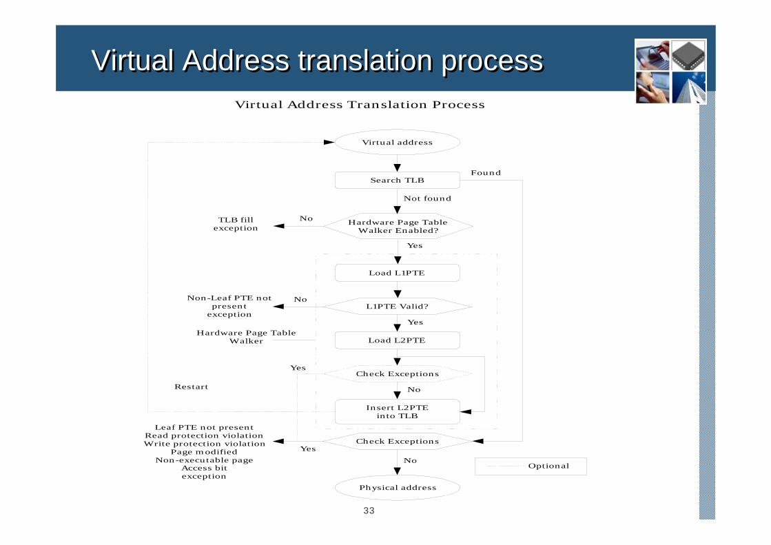
Virtual Address translation processVirtual Address translation processVirtual Address Translation Process
Virtual address
Search TLB
Hardware Page TableWalker Enabled?
Not found
NoTLB fillexception
Load L1PTE
Yes
L1PTE Valid?NoNon-Leaf PTE not
presentexception
Yes
Load L2PTE
Insert L2PTEinto TLB
Check Exceptions
No
Physical address
Yes
Leaf PTE not presentRead protection violationWrite protection violation
Page modifiedNon-executable page
Access bitexception
Found
Hardware Page TableWalker
Restart
Check Exceptions
No
Yes
Optional
34
AgendaAgenda
Andes Instruction Set Architecture Introduction32-bit Baseline Instructions16-bit Baseline InstructionsExtension Instructions
Andes System Privileged ArchitectureMemory Management UnitInterruption ArchitecturePerformance Monitoring MechanismLocal Memory InterfaceHigh Speed Memory Port SupportSystem Registers
back
35
Interruption IntroductionInterruption Introduction
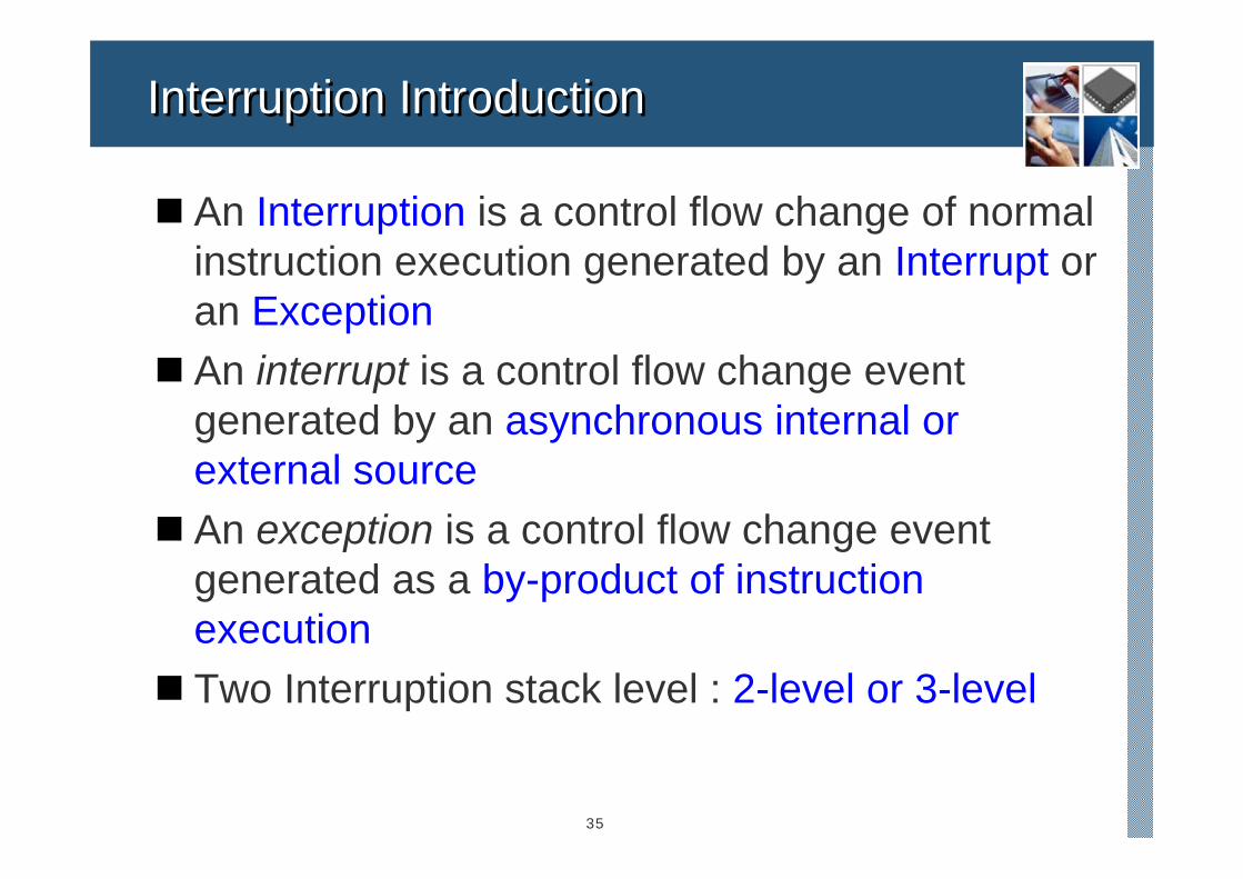
An Interruption is a control flow change of normal instruction execution generated by an Interrupt or an ExceptionAn interrupt is a control flow change event generated by an asynchronous internal or external sourceAn exception is a control flow change event generated as a by-product of instruction executionTwo Interruption stack level : 2-level or 3-level
36
Interruption Stack LevelInterruption Stack Level
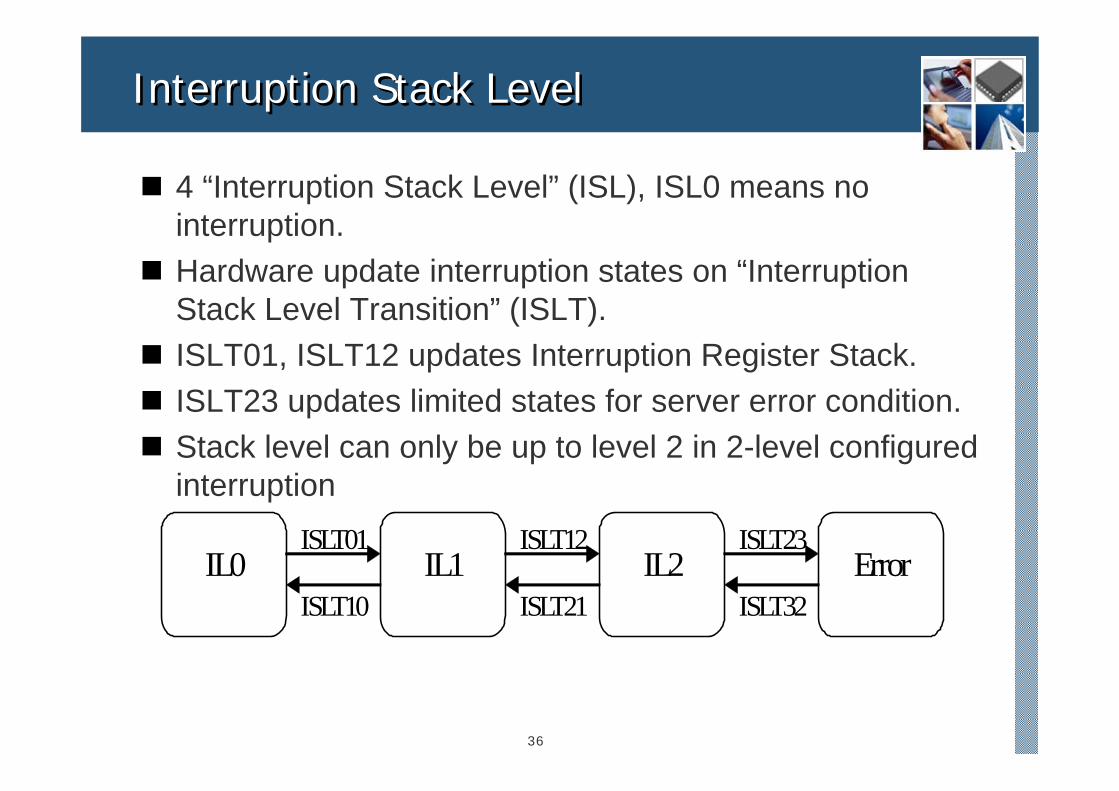
4 “Interruption Stack Level” (ISL), ISL0 means no interruption.Hardware update interruption states on “Interruption Stack Level Transition” (ISLT).ISLT01, ISLT12 updates Interruption Register Stack. ISLT23 updates limited states for server error condition.Stack level can only be up to level 2 in 2-level configured interruption
IL0 IL1 IL2 Error ISLT01
ISLT10
ISLT12
ISLT21
ISLT23
ISLT32
37
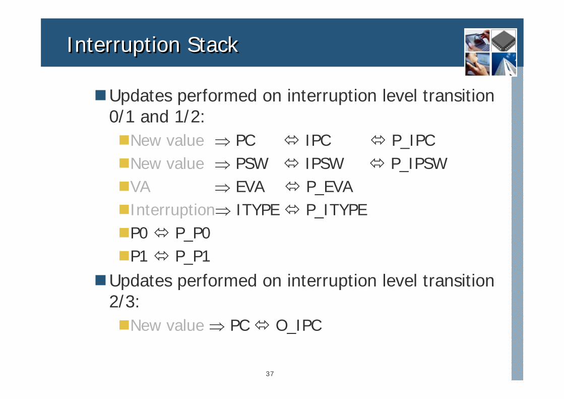
Interruption StackInterruption Stack
Updates performed on interruption level transition 0/1 and 1/2:
New value ⇒ PC IPC P_IPCNew value ⇒ PSW IPSW P_IPSWVA ⇒ EVA P_EVAInterruption⇒ ITYPE P_ITYPEP0 P_P0P1 P_P1
Updates performed on interruption level transition 2/3:
New value ⇒ PC O_IPC
38
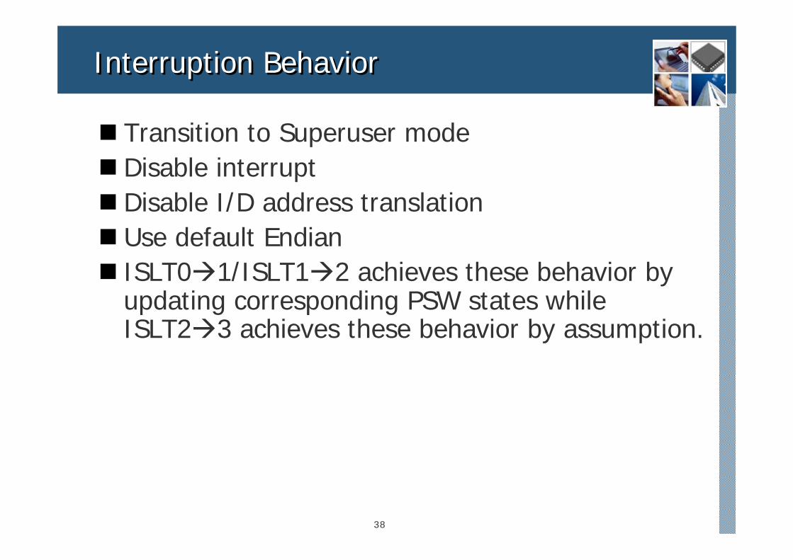
Interruption BehaviorInterruption Behavior
Transition to Superuser modeDisable interruptDisable I/D address translationUse default EndianISLT0 1/ISLT1 2 achieves these behavior by updating corresponding PSW states while ISLT2 3 achieves these behavior by assumption.
39
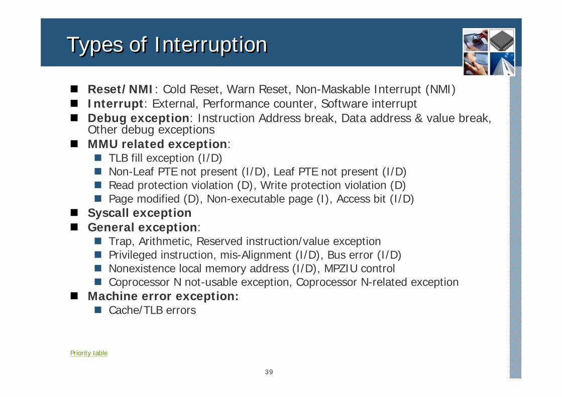
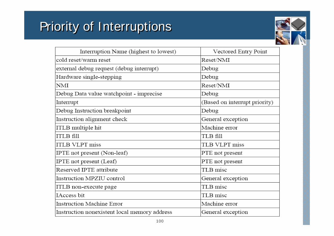
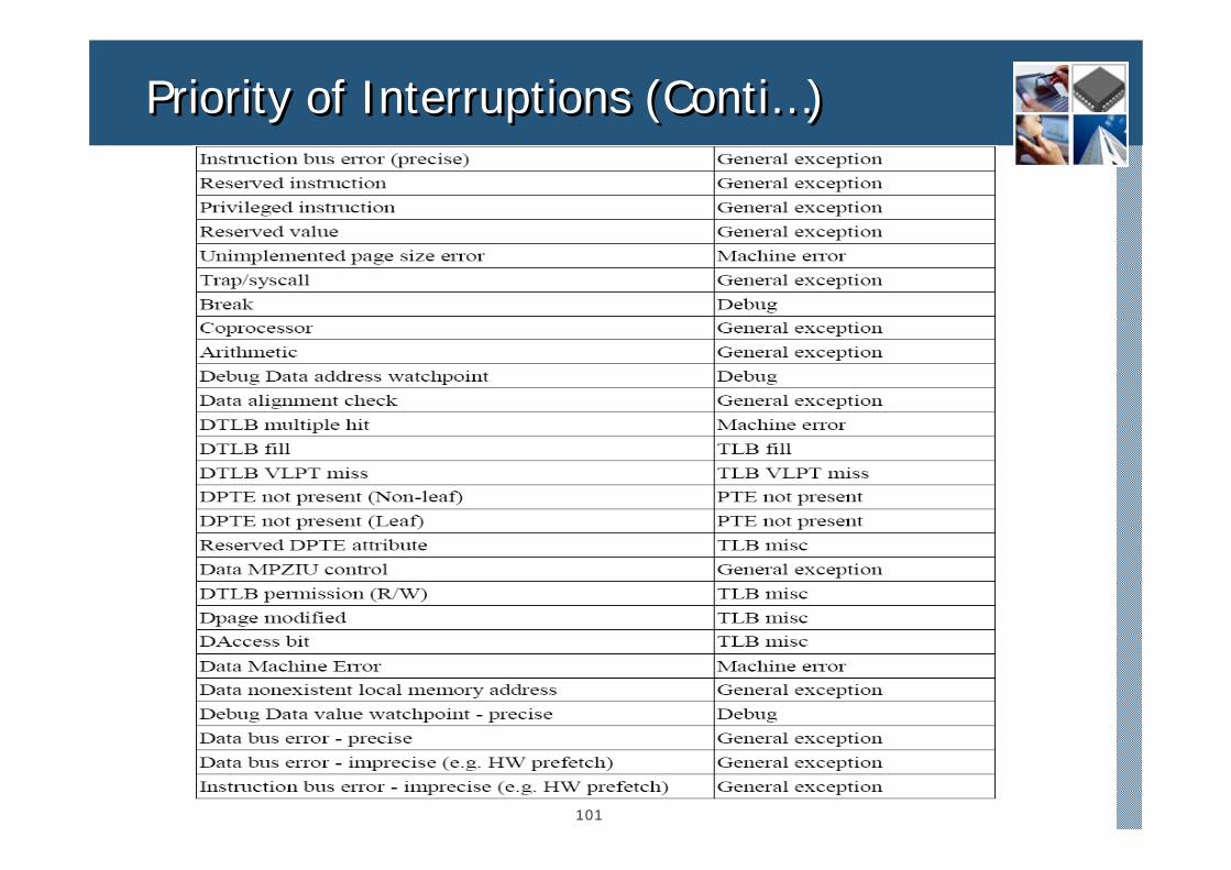
Types of InterruptionTypes of Interruption
Reset/NMI: Cold Reset, Warn Reset, Non-Maskable Interrupt (NMI)Interrupt: External, Performance counter, Software interruptDebug exception: Instruction Address break, Data address & value break, Other debug exceptions MMU related exception:
TLB fill exception (I/D)Non-Leaf PTE not present (I/D), Leaf PTE not present (I/D)Read protection violation (D), Write protection violation (D)Page modified (D), Non-executable page (I), Access bit (I/D)
Syscall exceptionGeneral exception:
Trap, Arithmetic, Reserved instruction/value exceptionPrivileged instruction, mis-Alignment (I/D), Bus error (I/D)Nonexistence local memory address (I/D), MPZIU controlCoprocessor N not-usable exception, Coprocessor N-related exception
Machine error exception:Cache/TLB errors
Priority table
40
Vectored Entry PointVectored Entry Point
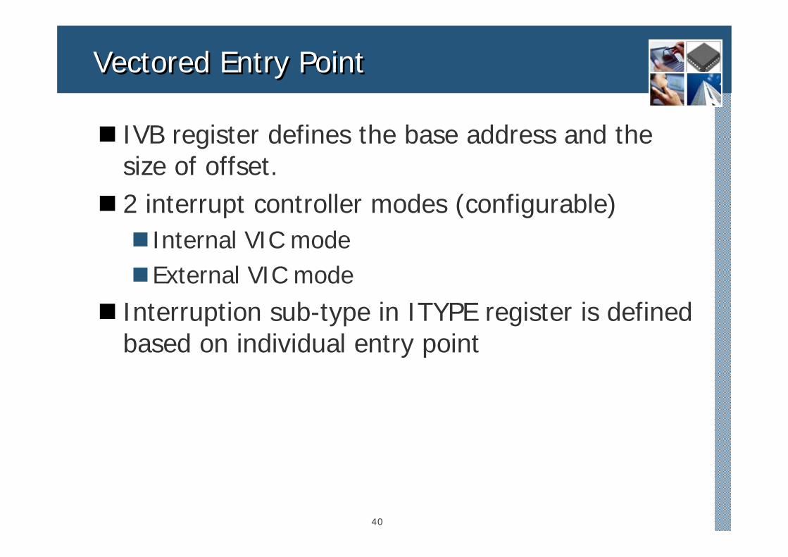
IVB register defines the base address and the size of offset.2 interrupt controller modes (configurable)
Internal VIC modeExternal VIC mode
Interruption sub-type in ITYPE register is defined based on individual entry point
41
Entry Point for IVIC/EVICEntry Point for IVIC/EVIC
Internal VIC mode16 entry points (9 exception + 7 interrupt)4 bits index
External VIC73 entry points (9 exception + 64 interrupt)7 bits index
SW 015
HW 0- 59 -14
Syscall8
General exception7
Debug related6
Machine Error5
Reserved4
TLB misc3
PTE not present2
TLB fill1
Reset/NMI0
Entry pointOffset
VEP 0-639-72
Syscall8
General exception7
Debug related6
Machine Error5
Reserved4
TLB misc3
PTE not present2
TLB fill1
Reset/NMI0
Entry pointOffset

42
AgendaAgenda
Andes Instruction Set Architecture Introduction32-bit Baseline Instructions16-bit Baseline InstructionsExtension Instructions
Andes System Privileged ArchitectureMemory Management UnitInterruption ArchitecturePerformance Monitoring MechanismLocal Memory InterfaceHigh Speed Memory Port SupportSystem Registers
back
43
Performance MonitorPerformance Monitor
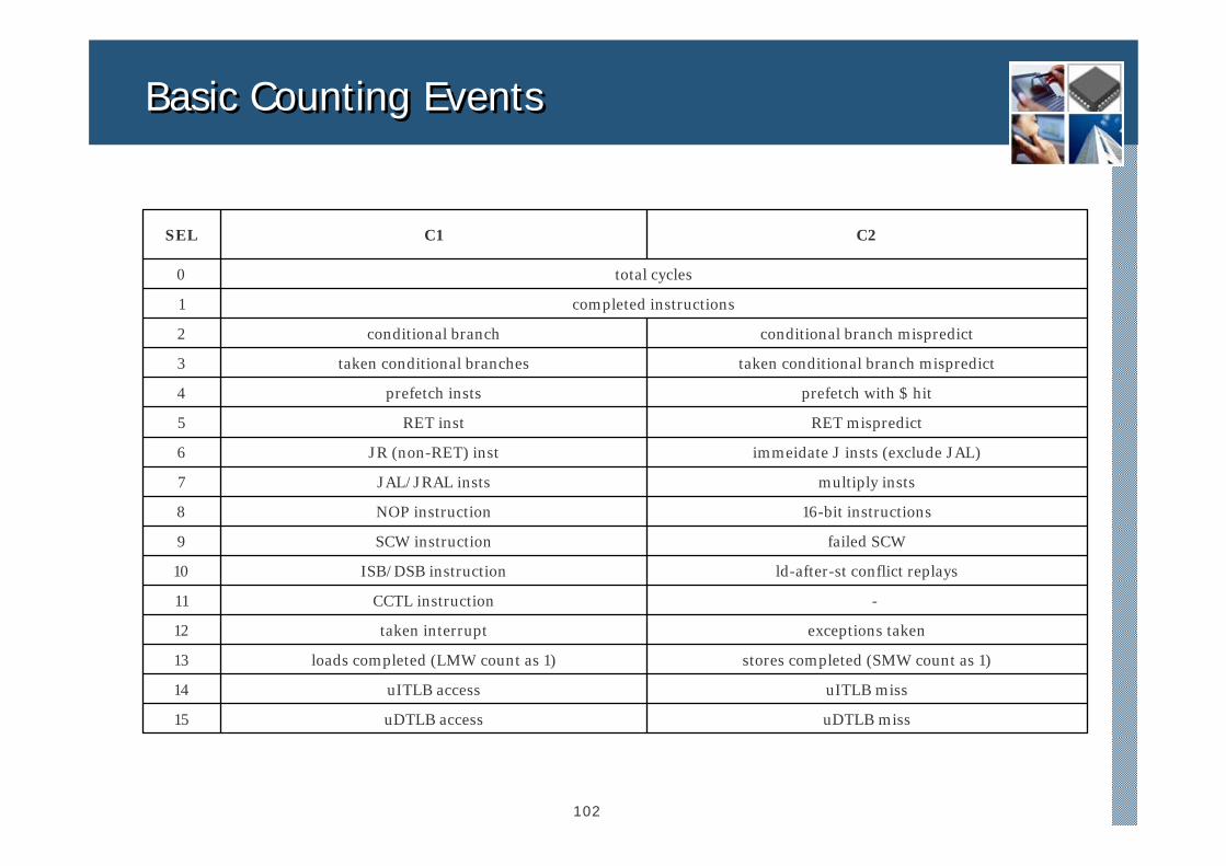
Mechanism to obtain program running statistics and performance data.Performance monitoring features:
One cycle/instruction counterTwo event countersIndividual controls:
Counter enableInterrupt enableOverflow status/clear bitCounting event selection among maximum of 64 eventsSuperuser and user mode event counting filters.
Readable/Writable in privileged modeContinuing counting after overflow
44
Counting EventsCounting Events
Instruction countsBranch, RET, JAL,PREF, ISB/DSB…
Program flow eventstaken branches, mispredict, interrupt, exception…
MMU eventsMTLB/uITLB/uDTLB access/misss, HPTWK cycles…
Cache eventsLoad/Store I/D cache access/miss…
Other eventsILM/DLM access, DMA cycles…
45
AgendaAgenda
Andes Instruction Set Architecture Introduction32-bit Baseline Instructions16-bit Baseline InstructionsExtension Instructions
Andes System Privileged ArchitectureMemory Management UnitInterruption ArchitecturePerformance Monitoring MechanismLocal Memory InterfaceHigh Speed Memory Port SupportSystem Registers
back
46
Local Memory and Local Memory DMALocal Memory and Local Memory DMA
Local memory is on-chip memories that are as fast as L1 caches.The local memory DMA is provided to transfer blocks of data between Andes core LM and external, off-core, memory in parallel with the Andes core execution pipeline.To transfer large amounts of data to or from LM, it is more efficient to use the DMA engine instead of the Andes core load/store instructions.
47
Local Memory (LM)Local Memory (LM)
The base address is aligned on 1MB boundary.The size is implementation depended.
4KB, 8KB, 16KB ~ 1024KBThe DLM support Double-buffer mode
DLM is divided into two banks.One for processor and the other for DMA.Processor and DMA can access the same address simultaneously.
Both Internal LM and External LM are supported
48
Local Memory DMALocal Memory DMA
Two channels Programmed using physical addressing Software takes care of address translation and permission check Only accessed by privileged modeFor both instruction and data local memory External address can be incremented with stride Aligned internal address Aligned external address for basic configuration Un-aligned External Address (UNEA) feature which allows un-aligned external address for element transfer2-D Element Transfer (2DET) feature which provides an easy way to transfer two-dimensional blocks from external memory
49
AgendaAgenda
Andes Instruction Set Architecture Introduction32-bit Baseline Instructions16-bit Baseline InstructionsExtension Instructions
Andes System Privileged ArchitectureMemory Management UnitInterruption ArchitecturePerformance Monitoring MechanismLocal Memory InterfaceHigh Speed Memory Port SupportSystem Registers
back
50
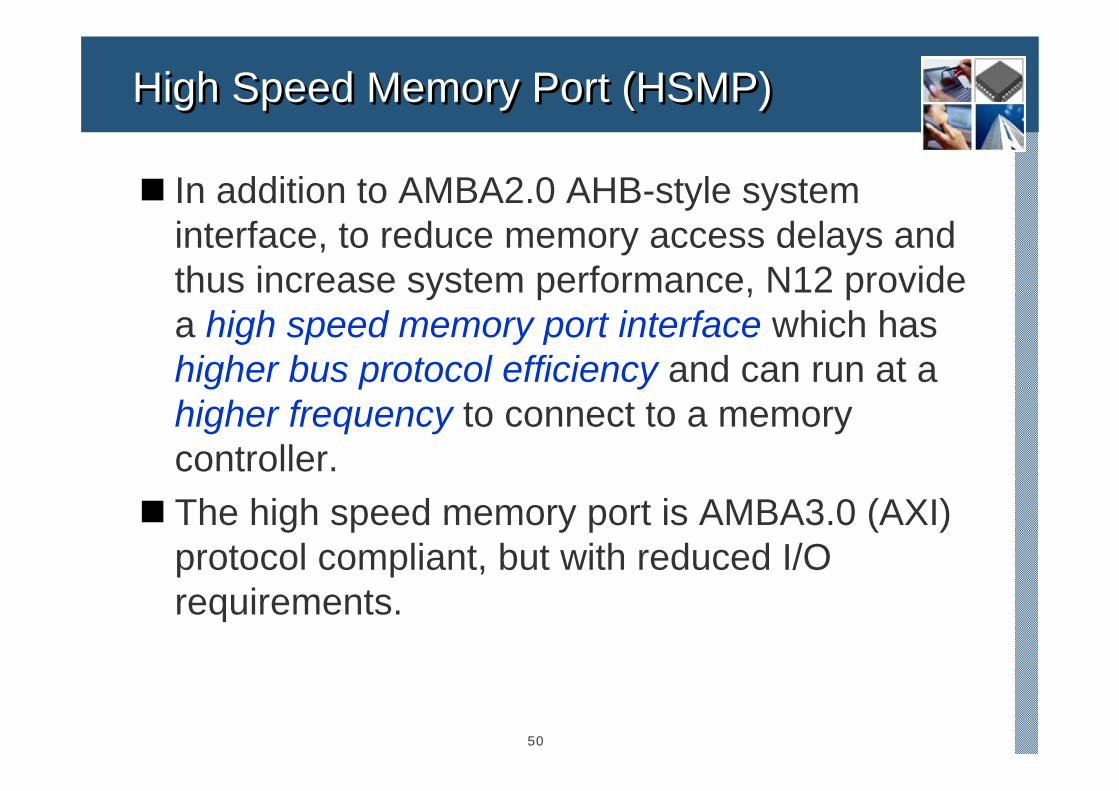
High Speed Memory Port (HSMP)High Speed Memory Port (HSMP)
In addition to AMBA2.0 AHB-style system interface, to reduce memory access delays and thus increase system performance, N12 provide a high speed memory port interface which has higher bus protocol efficiency and can run at a higher frequency to connect to a memory controller.The high speed memory port is AMBA3.0 (AXI) protocol compliant, but with reduced I/O requirements.
51
AgendaAgenda
Andes Instruction Set Architecture Introduction32-bit Baseline Instructions16-bit Baseline InstructionsExtension Instructions
Andes System Privileged ArchitectureMemory Management UnitInterruption ArchitecturePerformance Monitoring MechanismLocal Memory InterfaceHigh Speed Memory Port SupportSystem Registers
back
52
System RegistersSystem Registers
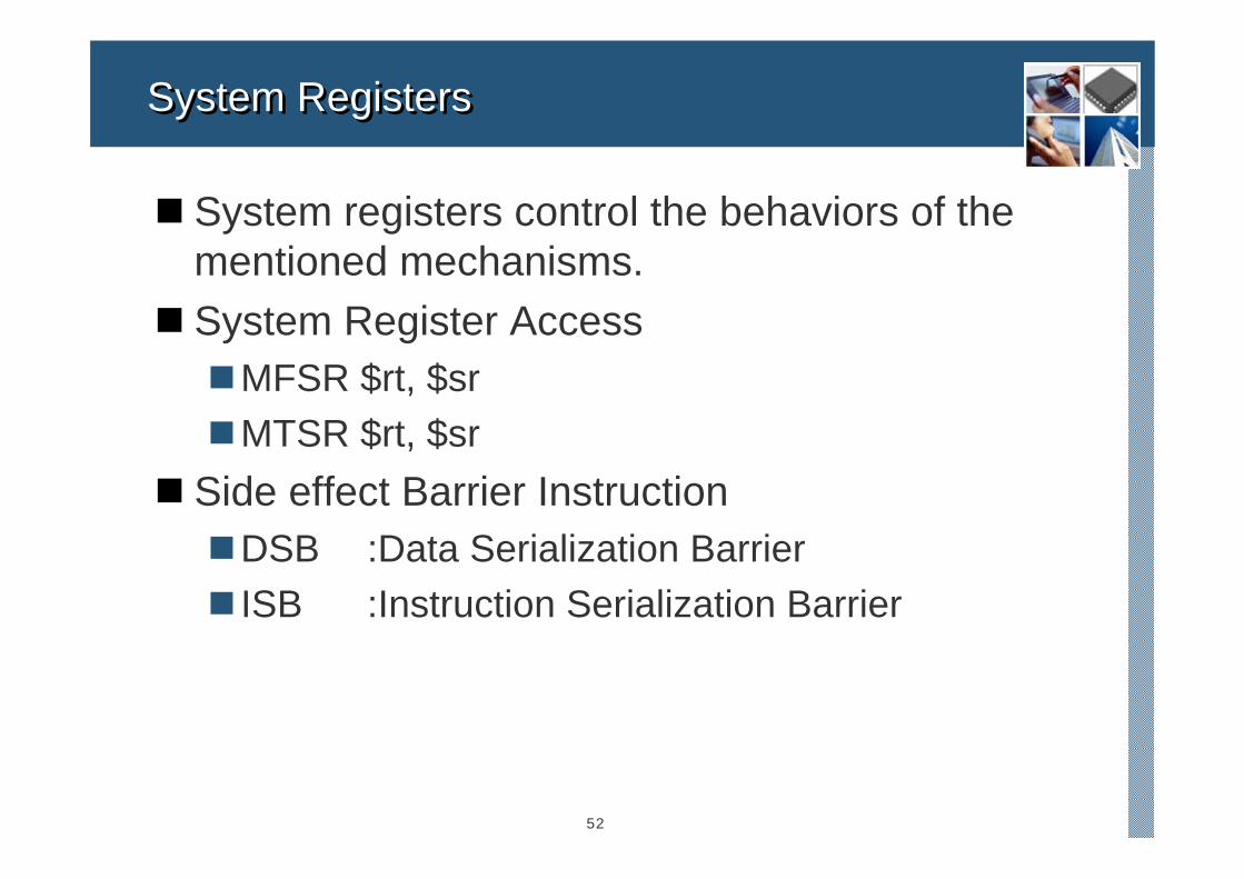
System registers control the behaviors of the mentioned mechanisms.System Register Access
MFSR $rt, $srMTSR $rt, $sr
Side effect Barrier Instruction DSB :Data Serialization Barrier ISB :Instruction Serialization Barrier
53
Configuration System RegistersConfiguration System Registers
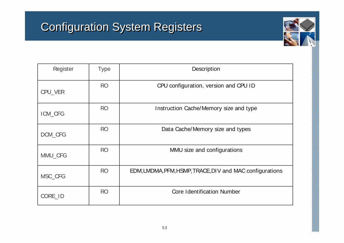
Core Identification NumberROCORE_ID
EDM,LMDMA,PFM,HSMP,TRACE,DIV and MAC configurationsROMSC_CFG
MMU size and configurationsROMMU_CFG
Data Cache/Memory size and typesRODCM_CFG
Instruction Cache/Memory size and typeROICM_CFG
CPU configuration, version and CPU IDROCPU_VER
DescriptionTypeRegister
54
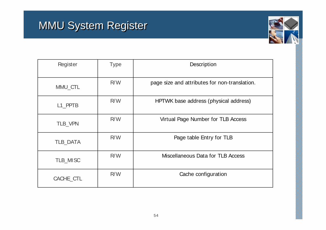
MMU System RegisterMMU System Register
Cache configurationR/WCACHE_CTL
Miscellaneous Data for TLB AccessR/WTLB_MISC
Page table Entry for TLBR/WTLB_DATA
Virtual Page Number for TLB AccessR/WTLB_VPN
HPTWK base address (physical address)R/WL1_PPTB
page size and attributes for non-translation.R/WMMU_CTL
DescriptionTypeRegister
55
Interruption System RegisterInterruption System Register
Interruption PendingR/WINT_PEND
Interruption MaskingR/WINT_MASK
Level 2 P0 - 1 stack R/WP_P0 - P_P1
Overflow PC used for ILT23 R/WOIPC
Level 2 PC stackR/WP_IPC
Level 1 PC stackR/WIPC
Machine Error logR/WMERR
Level 2 ITPE stackR/WP_ITYPE
Type of InterruptionROITYPE
Level 2 EVA stackR/WP_EVA
Virtual address which causes the exceptionROEVA
Base address of the interruption vector tableR/WIVB
Level 2 PSW stack R/WP_IPSW
Level 1 PSW stack R/WIPSW
Processor Status Control/Status R/WPSW
DescriptionTypeRegister
56
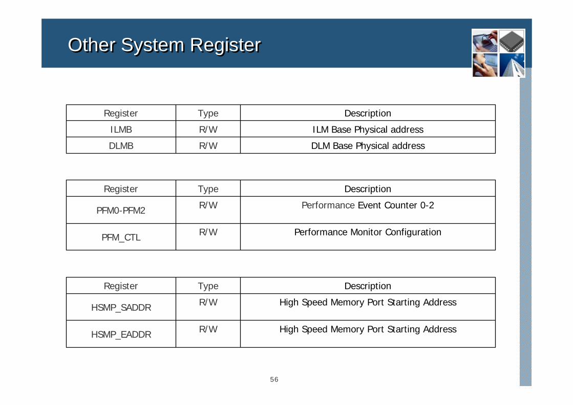
Other System RegisterOther System Register
High Speed Memory Port Starting AddressR/WHSMP_EADDR
High Speed Memory Port Starting AddressR/WHSMP_SADDR
DescriptionTypeRegister
Performance Monitor ConfigurationR/WPFM_CTL
Performance Event Counter 0-2R/WPFM0-PFM2
DescriptionTypeRegister
DLM Base Physical addressR/WDLMB
ILM Base Physical addressR/WILMB
DescriptionTypeRegister

Thank You!!!Thank You!!!
58
The following are spare slides…
59
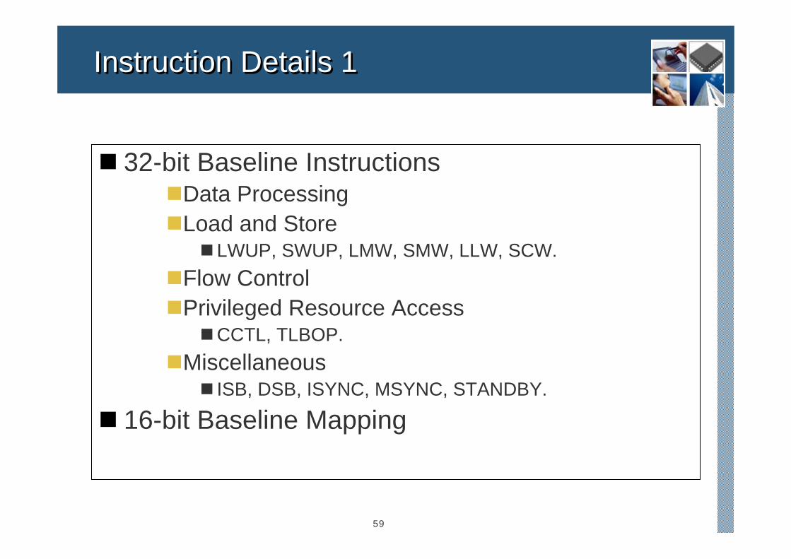
Instruction Details 1Instruction Details 1
32-bit Baseline InstructionsData ProcessingLoad and Store
LWUP, SWUP, LMW, SMW, LLW, SCW.Flow ControlPrivileged Resource Access
CCTL, TLBOP. Miscellaneous
ISB, DSB, ISYNC, MSYNC, STANDBY.
16-bit Baseline Mapping
60
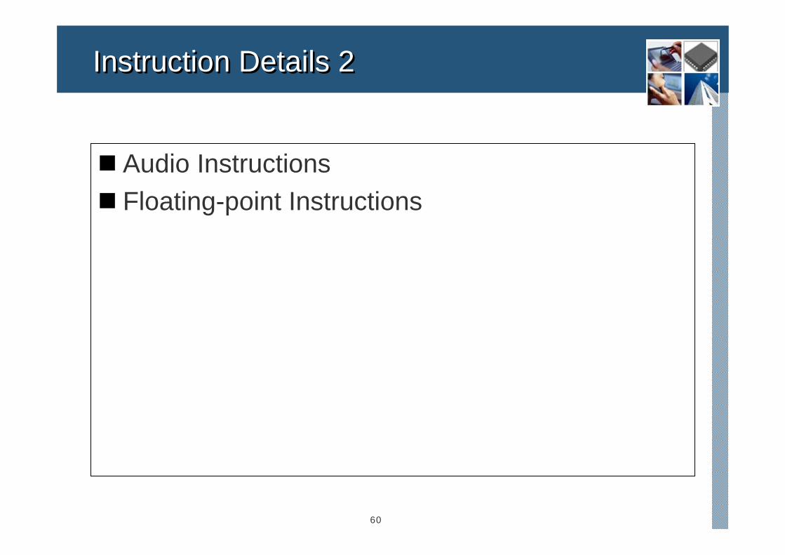
Instruction Details 2Instruction Details 2
Audio InstructionsFloating-point Instructions
61
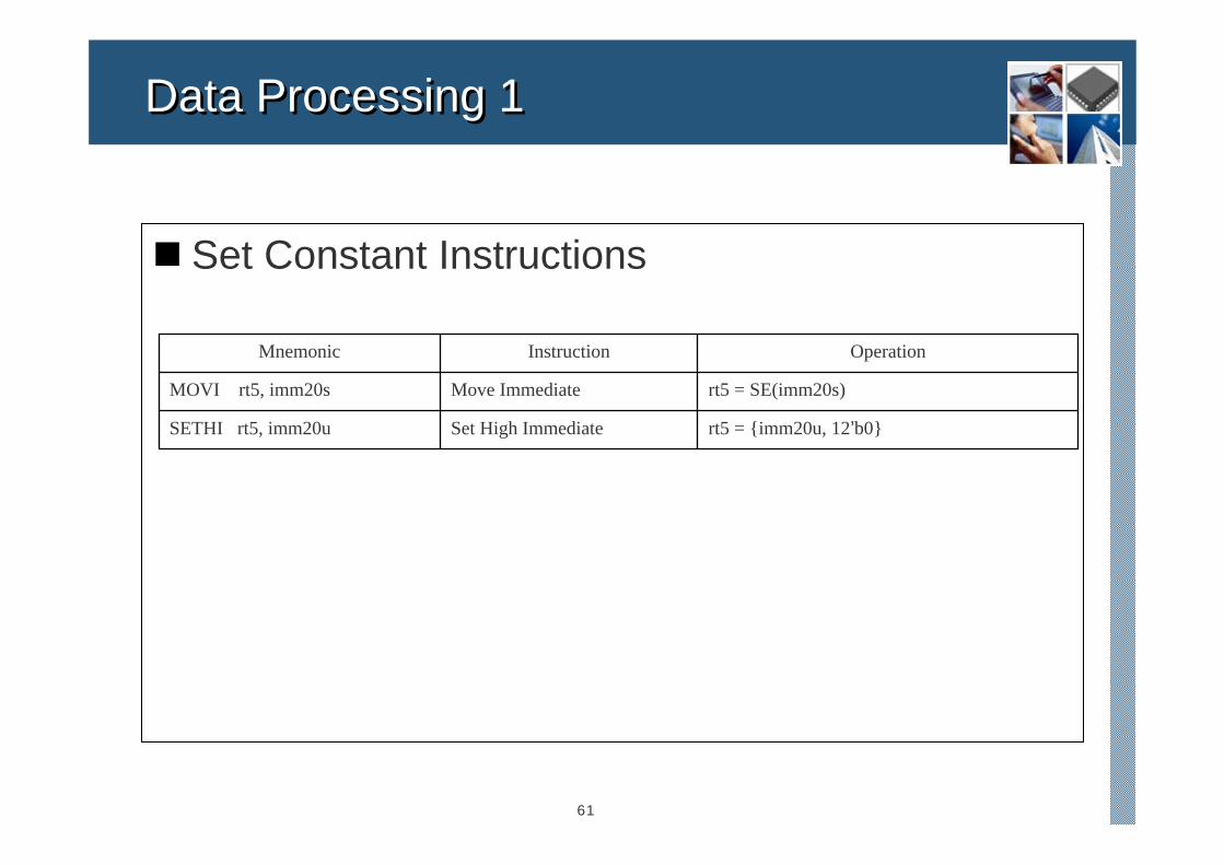
Data Processing 1Data Processing 1
Set Constant Instructions
rt5 = {imm20u, 12’b0}Set High ImmediateSETHI rt5, imm20u
rt5 = SE(imm20s)Move ImmediateMOVI rt5, imm20s
OperationInstructionMnemonic
62
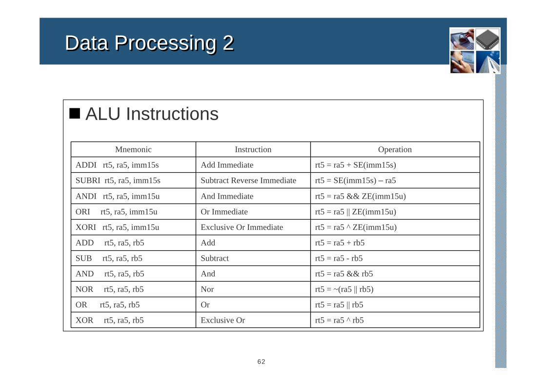
Data Processing 2Data Processing 2
ALU Instructions
rt5 = ra5 ^ rb5Exclusive OrXOR rt5, ra5, rb5
rt5 = ra5 || rb5OrOR rt5, ra5, rb5
rt5 = ~(ra5 || rb5)NorNOR rt5, ra5, rb5
rt5 = ra5 && rb5AndAND rt5, ra5, rb5
rt5 = ra5 - rb5SubtractSUB rt5, ra5, rb5
rt5 = ra5 + rb5AddADD rt5, ra5, rb5
rt5 = ra5 ^ ZE(imm15u)Exclusive Or ImmediateXORI rt5, ra5, imm15u
rt5 = ra5 || ZE(imm15u)Or ImmediateORI rt5, ra5, imm15u
rt5 = ra5 && ZE(imm15u)And ImmediateANDI rt5, ra5, imm15u
rt5 = SE(imm15s) – ra5Subtract Reverse ImmediateSUBRI rt5, ra5, imm15s
rt5 = ra5 + SE(imm15s)Add ImmediateADDI rt5, ra5, imm15s
OperationInstructionMnemonic
63
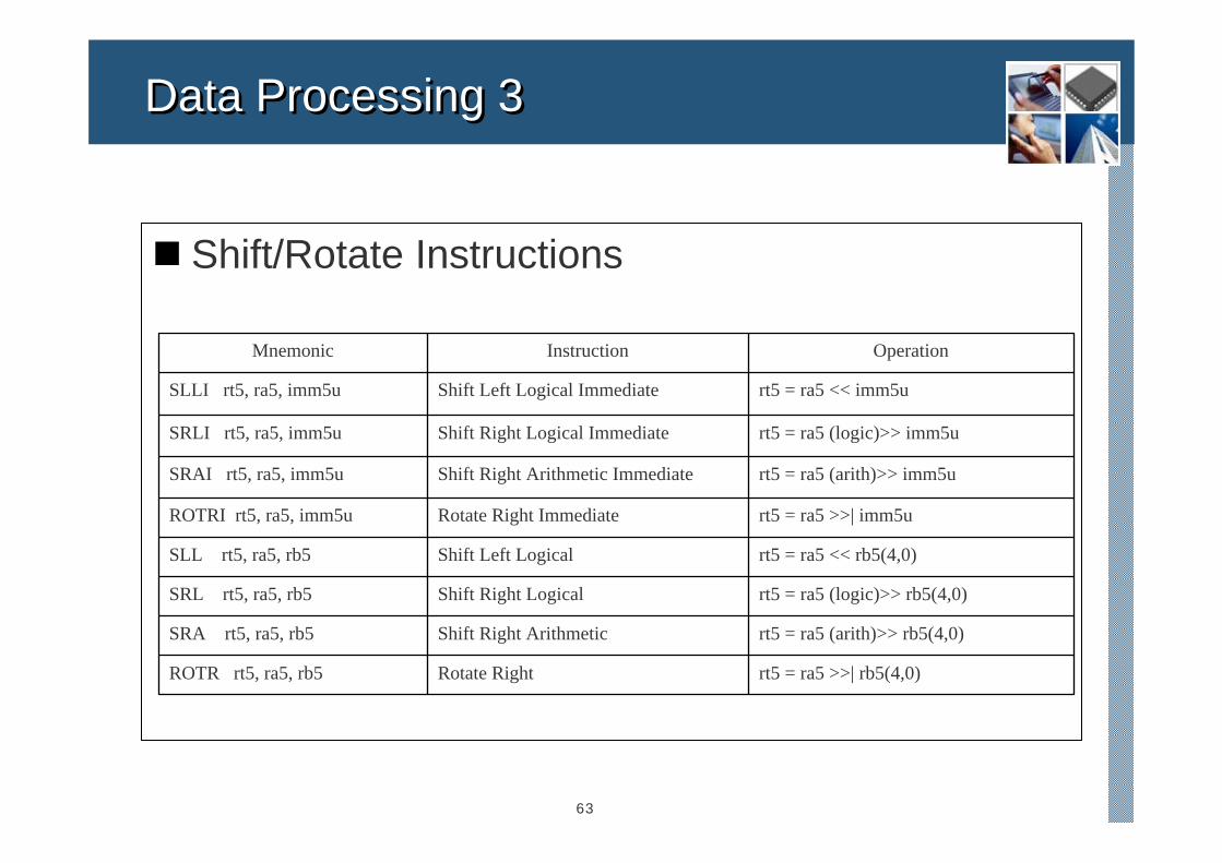
Data Processing 3Data Processing 3
Shift/Rotate Instructions
rt5 = ra5 >>| rb5(4,0)Rotate RightROTR rt5, ra5, rb5
rt5 = ra5 (arith)>> rb5(4,0)Shift Right ArithmeticSRA rt5, ra5, rb5
rt5 = ra5 (logic)>> rb5(4,0)Shift Right LogicalSRL rt5, ra5, rb5
rt5 = ra5 << rb5(4,0)Shift Left LogicalSLL rt5, ra5, rb5
rt5 = ra5 >>| imm5uRotate Right ImmediateROTRI rt5, ra5, imm5u
rt5 = ra5 (arith)>> imm5uShift Right Arithmetic ImmediateSRAI rt5, ra5, imm5u
rt5 = ra5 (logic)>> imm5uShift Right Logical ImmediateSRLI rt5, ra5, imm5u
rt5 = ra5 << imm5uShift Left Logical ImmediateSLLI rt5, ra5, imm5u
OperationInstructionMnemonic
64
Data Processing 4Data Processing 4
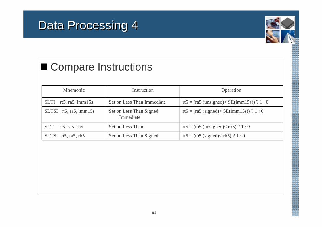
Compare Instructions
rt5 = (ra5 (signed)< rb5) ? 1 : 0Set on Less Than SignedSLTS rt5, ra5, rb5
rt5 = (ra5 (unsigned)< rb5) ? 1 : 0Set on Less ThanSLT rt5, ra5, rb5
rt5 = (ra5 (signed)< SE(imm15s)) ? 1 : 0Set on Less Than Signed Immediate
SLTSI rt5, ra5, imm15s
rt5 = (ra5 (unsigned)< SE(imm15s)) ? 1 : 0Set on Less Than ImmediateSLTI rt5, ra5, imm15s
OperationInstructionMnemonic
65
Data Processing 5Data Processing 5
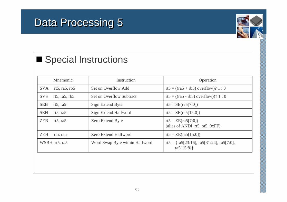
Special Instructions
rt5 = {ra5[23:16], ra5[31:24], ra5[7:0], ra5[15:8]}
Word Swap Byte within HalfwordWSBH rt5, ra5
rt5 = ZE(ra5[15:0])Zero Extend HalfwordZEH rt5, ra5
rt5 = ZE(ra5[7:0])(alias of ANDI rt5, ra5, 0xFF)
Zero Extend ByteZEB rt5, ra5
rt5 = SE(ra5[15:0])Sign Extend HalfwordSEH rt5, ra5
rt5 = SE(ra5[7:0])Sign Extend ByteSEB rt5, ra5
rt5 = ((ra5 - rb5) overflow))? 1 : 0Set on Overflow SubtractSVS rt5, ra5, rb5
rt5 = ((ra5 + rb5) overflow)? 1 : 0Set on Overflow AddSVA rt5, ra5, rb5
OperationInstructionMnemonic
66
Data Processing 6Data Processing 6
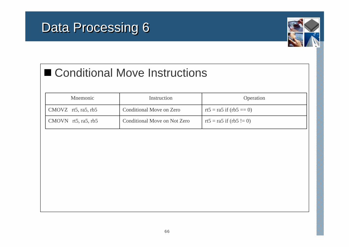
Conditional Move Instructions
rt5 = ra5 if (rb5 != 0)Conditional Move on Not ZeroCMOVN rt5, ra5, rb5
rt5 = ra5 if (rb5 == 0)Conditional Move on ZeroCMOVZ rt5, ra5, rb5
OperationInstructionMnemonic
67
Data Processing 7Data Processing 7
MFUSR and MTUSR (Group 0)
USReg[USR] = rt5Move To User Special RegisterMTUSR rt5, USR
rt5 = USReg[USR]Move From User Special RegisterMFUSR rt5, USR
OperationInstructionMnemonic
PC(The PC value of this instruction)
310
Reserved30-40
D1.HI30
D1.LO20
D0.HI10
D0.LO00
User Special RegisterUSR valueGroup
68
Load and Store 1Load and Store 1
address = ra5 + SE(imm15s)Byte-memory(address) = rt5[7:0]
Store Byte ImmediateSBI rt5, [ra5 + imm15s]
address = ra5 + SE(imm15s << 1)Halfword-memory(address) = rt5[15:0]
Store Halfword ImmediateSHI rt5, [ra5 + (imm15s << 1)]
address = ra5 + SE(imm15s << 2)Word-memory(address) = rt5
Store Word ImmediateSWI rt5, [ra5 + (imm15s << 2)]
address = ra5 + SE(imm15s)rt5 = SE(Byte-memory(address))
Load Byte Signed ImmediateLBSI rt5, [ra5 + imm15s]
address = ra5 + SE(imm15s)rt5 = ZE(Byte-memory(address))
Load Byte ImmediateLBI rt5, [ra5 + imm15s]
address = ra5 + SE(imm15s << 1)rt5 = SE(Halfword-memory(address))
Load Halfword Signed ImmediateLHSI rt5, [ra5 + (imm15s << 1)]
address = ra5 + SE(imm15s << 1)rt5 = ZE(Halfword-memory(address))
Load Halfword ImmediateLHI rt5, [ra5 + (imm15s << 1)]
address = ra5 + SE(imm15s << 2)rt5 = Word-memory(address)
Load Word ImmediateLWI rt5, [ra5 + (imm15s << 2)]
OperationInstructionMnemonic
69
Load and Store 2Load and Store 2
Byte-memory(ra5) = rt5[7:0]ra5 = ra5 + SE(imm15s)
Store Byte Immediate with Post Increment
SBI.bi rt5, [ra5],imm15s
Halfword-memory(ra5) = rt5[15:0]ra5 = ra5 + SE(imm15s << 1)
Store Halfword Immediate with Post Increment
SHI.bi rt5, [ra5],(imm15s << 1)
Word-memory(ra5) = rt5ra5 = ra5 + SE(imm15s << 2)
Store Word Immediate with Post Increment
SWI.bi rt5, [ra5],(imm15s << 2)
rt5 = SE(Byte-memory(ra5))ra5 = ra5 + SE(imm15s)
Load Byte Signed Immediate with Post Increment
LBSI.bi rt5, [ra5],imm15s
rt5 = ZE(Byte-memory(ra5))ra5 = ra5 + SE(imm15s)
Load Byte Immediate with Post Increment
LBI.bi rt5, [ra5],imm15s
rt5 = SE(Halfword-memory(ra5))ra5 = ra5 + SE(imm15s << 1)
Load Halfword Signed Immediate with Post Increment
LHSI.bi rt5, [ra5],(imm15s << 1)
rt5 = ZE(Halfword-memory(ra5))ra5 = ra5 + SE(imm15s << 1)
Load Halfword Immediate with Post Increment
LHI.bi rt5, [ra5],(imm15s << 1)
rt5 = Word-memory(ra5)ra5 = ra5 + SE(imm15s << 2)
Load Word Immediate with Post Increment
LWI.bi rt5, [ra5],(imm15s << 2)
OperationInstructionMnemonic
70
Load and Store 3Load and Store 3
address = ra5 + (rb5 << sv)Byte-memory(address) = rt5[7:0]
Store ByteSB rt5, [ra5 + (rb5 << sv)]
address = ra5 + (rb5 << sv)Halfword-memory(address) = rt5[15:0]
Store HalfwordSH rt5, [ra5 + (rb5 << sv)]
address = ra5 + (rb5 << sv)Word-memory(address) = rt5
Store WordSW rt5, [ra5 + (rb5 << sv)]
address = ra5 + (rb5 << sv)rt5 = SE(Byte-memory(address))
Load Byte SignedLBS rt5, [ra5 + (rb5 << sv)]
address = ra5 + (rb5 << sv)rt5 = ZE(Byte-memory(address))
Load ByteLB rt5, [ra5 + (rb5 << sv)]
address = ra5 + (rb5 << sv)rt5 = SE(Halfword-memory(address))
Load Halfword SignedLHS rt5, [ra5 + (rb5 << sv)]
address = ra5 + (rb5 << sv)rt5 = ZE(Halfword-memory(address))
Load HalfwordLH rt5, [ra5 + (rb5 << sv)]
address = ra5 + (rb5 << sv)rt5 = Word-memory(address)
Load WordLW rt5, [ra5 + (rb5 << sv)]
OperationInstructionMnemonic
71
Load and Store 4Load and Store 4
Byte-memory(ra5) = rt5[7:0]ra5 = ra5 + (rb5 << sv)
Store Byte with Post IncrementSB.bi rt5, [ra5],rb5<<sv
Halfword-memory(ra5) = rt5[15:0]ra5 = ra5 + (rb5 << sv)
Store Halfword with Post IncrementSH.bi rt5, [ra5],rb5<<sv
Word-memory(ra5) = rt5ra5 = ra5 + (rb5 << sv)
Store Word with Post IncrementSW.bi rt5, [ra5],rb5<<sv
rt5 = SE(Byte-memory(ra5))ra5 = ra5 + (rb5 << sv)
Load Byte Signed with Post Increment
LBS.bi rt5, [ra5],rb5<<sv
rt5 = ZE(Byte-memory(ra5))ra5 = ra5 + (rb5 << sv)
Load Byte with Post IncrementLB.bi rt5, [ra5],rb5<<sv
rt5 = SE(Halfword-memory(ra5))ra5 = ra5 + (rb5 << sv)
Load Halfword Signed with Post Increment
LHS.bi rt5, [ra5],rb5<<sv
rt5 = ZE(Halfword-memory(ra5))ra5 = ra5 + (rb5 << sv)
Load Halfword with Post IncrementLH.bi rt5, [ra5],rb5<<sv
rt5 = Word-memory(ra5)ra5 = ra5 + (rb5 << sv)
Load Word with Post IncrementLW.bi rt5, [ra5],rb5<<sv
OperationInstructionMnemonic
72
LWUP and SWUPLWUP and SWUP
UsageTo access a 32-bit word between memory and GPR with the user mode privilege address translation.To use the user-mode privilege address translation regardless of the current processor operation mode (PSW.POM) and the current data address translation state (PSW.DT).
back
73
LMW and SMWLMW and SMW
UsageTo load/store multiple 32-bit words from/to sequential memory locations.
00mi:0d:1
b:0a:1
SMW1
Enable4ReRaRbLSMW011101
0
00mi:0d:1
b:0a:1
LMW0
Enable4ReRaRbLSMW011101
0
1 023459 614 1019 1524 2030 2531
74
LLW and SCWLLW and SCW
UsageTo implement a primitive to perform atomic read-modify-write operations.
LLW sets a lock flag while loading data.SCW checks the lock flags before storing data and returns the status bit and write to GPR.
ExampleLLW Rx… Modifying RxSCW RxBEQZ Rx
back
75
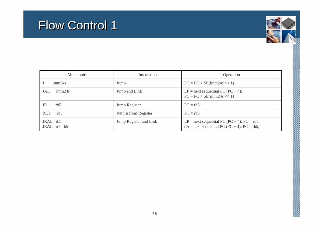
Flow Control 1Flow Control 1
LP = next sequential PC (PC + 4); PC = rb5;rt5 = next sequential PC (PC + 4); PC = rb5;
Jump Register and LinkJRAL rb5JRAL rt5, rb5
PC = rb5Return from RegisterRET rb5
PC = rb5Jump RegisterJR rb5
LP = next sequential PC (PC + 4);PC = PC + SE(imm24s << 1)
Jump and LinkJAL imm24s
PC = PC + SE(imm24s << 1)JumpJ imm24s
OperationInstructionMnemonic
76
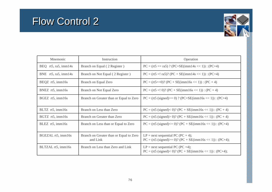
Flow Control 2Flow Control 2
LP = next sequential PC (PC +4);PC = (rt5 (signed)< 0)? (PC + SE(imm16s << 1)) : (PC+4);
Branch on Less than Zero and LinkBLTZAL rt5, imm16s
LP = next sequential PC (PC + 4);PC = (rt5 (signed)>= 0)? (PC + SE(imm16s << 1)) : (PC+4);
Branch on Greater than or Equal to Zero and Link
BGEZAL rt5, imm16s
PC = (rt5 (signed)<= 0)? (PC + SE(imm16s << 1)) : (PC+4)Branch on Less than or Equal to ZeroBLEZ rt5, imm16s
PC = (rt5 (signed)> 0)? (PC + SE(imm16s << 1)) : (PC + 4)Branch on Greater than ZeroBGTZ rt5, imm16s
PC = (rt5 (signed)< 0)? (PC + SE(imm16s << 1)) : (PC + 4)Branch on Less than ZeroBLTZ rt5, imm16s
PC = (rt5 (signed)>= 0) ? (PC+SE(imm16s << 1)) : (PC+4)Branch on Greater than or Equal to ZeroBGEZ rt5, imm16s
PC = (rt5 =! 0)? (PC + SE(imm16s << 1)) : (PC + 4)Branch on Not Equal ZeroBNEZ rt5, imm16s
PC = (rt5==0)? (PC + SE(imm16s << 1)) : (PC + 4)Branch on Equal ZeroBEQZ rt5, imm16s
PC = (rt5 =! ra5)? (PC + SE(imm14s << 1)) : (PC+4)Branch on Not Equal ( 2 Register )BNE rt5, ra5, imm14s
PC = (rt5 == ra5) ? (PC+SE(imm14s << 1)) : (PC+4)Branch on Equal ( 2 Register )BEQ rt5, ra5, imm14s
OperationInstructionMnemonic
77
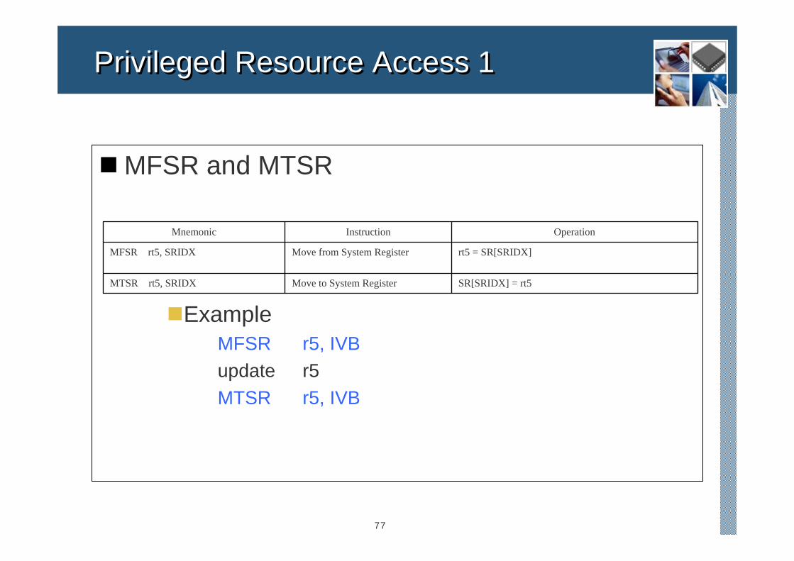
Privileged Resource Access 1Privileged Resource Access 1
MFSR and MTSR
ExampleMFSR r5, IVBupdate r5MTSR r5, IVB
SR[SRIDX] = rt5Move to System RegisterMTSR rt5, SRIDX
rt5 = SR[SRIDX]Move from System RegisterMFSR rt5, SRIDX
OperationInstructionMnemonic
78
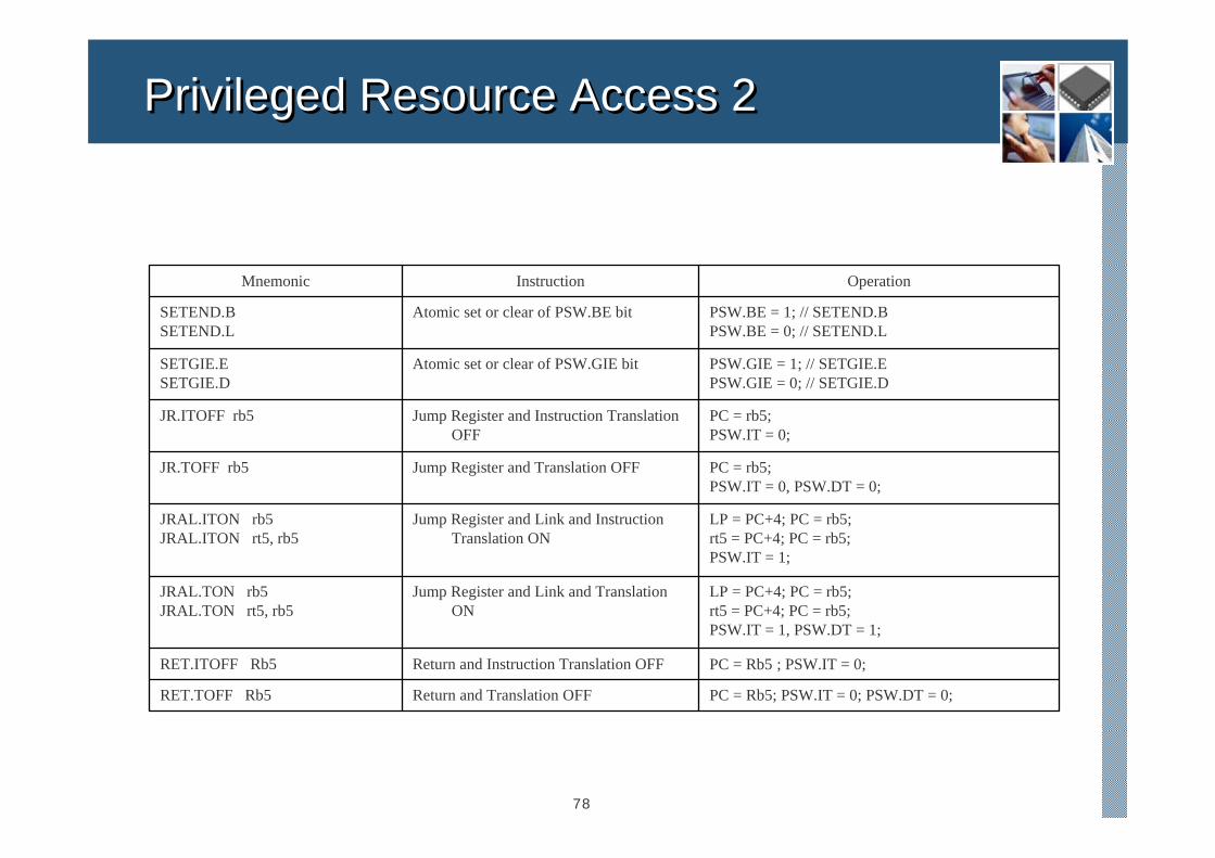
Privileged Resource Access 2Privileged Resource Access 2
PC = Rb5; PSW.IT = 0; PSW.DT = 0;Return and Translation OFFRET.TOFF Rb5
PC = Rb5 ; PSW.IT = 0;Return and Instruction Translation OFFRET.ITOFF Rb5
LP = PC+4; PC = rb5;rt5 = PC+4; PC = rb5;PSW.IT = 1, PSW.DT = 1;
Jump Register and Link and Translation ON
JRAL.TON rb5JRAL.TON rt5, rb5
LP = PC+4; PC = rb5;rt5 = PC+4; PC = rb5;PSW.IT = 1;
Jump Register and Link and Instruction Translation ON
JRAL.ITON rb5JRAL.ITON rt5, rb5
PC = rb5;PSW.IT = 0, PSW.DT = 0;
Jump Register and Translation OFFJR.TOFF rb5
PC = rb5;PSW.IT = 0;
Jump Register and Instruction Translation OFF
JR.ITOFF rb5
PSW.GIE = 1; // SETGIE.EPSW.GIE = 0; // SETGIE.D
Atomic set or clear of PSW.GIE bitSETGIE.ESETGIE.D
PSW.BE = 1; // SETEND.BPSW.BE = 0; // SETEND.L
Atomic set or clear of PSW.BE bitSETEND.BSETEND.L
OperationInstructionMnemonic
79
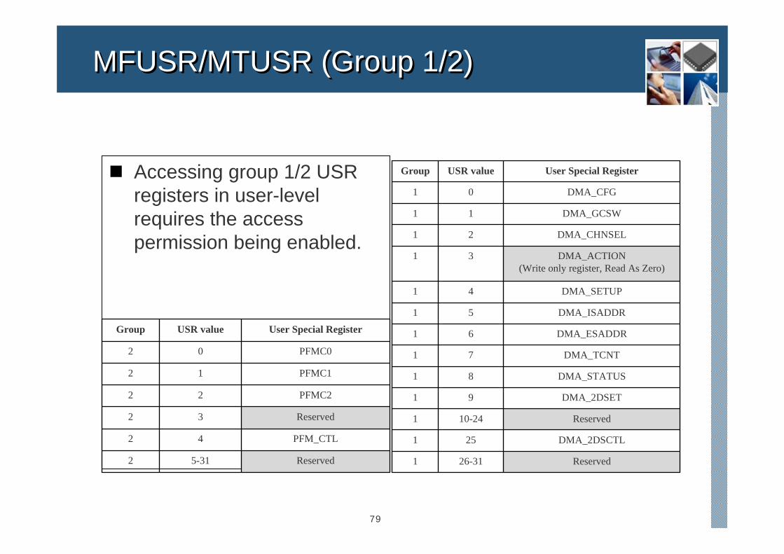
MFUSR/MTUSR (Group 1/2)MFUSR/MTUSR (Group 1/2)
Accessing group 1/2 USR registers in user-level requires the access permission being enabled.
Reserved26-311
DMA_2DSCTL251
Reserved10-241
DMA_2DSET91
DMA_STATUS81
DMA_TCNT71
DMA_ESADDR61
DMA_ISADDR51
DMA_SETUP41
DMA_ACTION(Write only register, Read As Zero)
31
DMA_CHNSEL21
DMA_GCSW11
DMA_CFG01
User Special RegisterUSR valueGroup
Reserved5-312
PFM_CTL 42
Reserved32
PFMC222
PFMC112
PFMC002
User Special RegisterUSR valueGroup
80
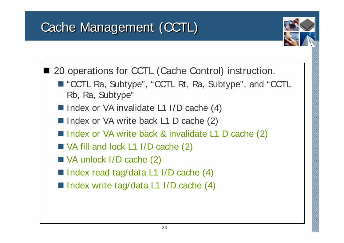
Cache Management (CCTL)Cache Management (CCTL)
20 operations for CCTL (Cache Control) instruction.“CCTL Ra, Subtype”, “CCTL Rt, Ra, Subtype”, and “CCTL Rb, Ra, Subtype”Index or VA invalidate L1 I/D cache (4)Index or VA write back L1 D cache (2)Index or VA write back & invalidate L1 D cache (2)VA fill and lock L1 I/D cache (2)VA unlock I/D cache (2)Index read tag/data L1 I/D cache (4)Index write tag/data L1 I/D cache (4)
81
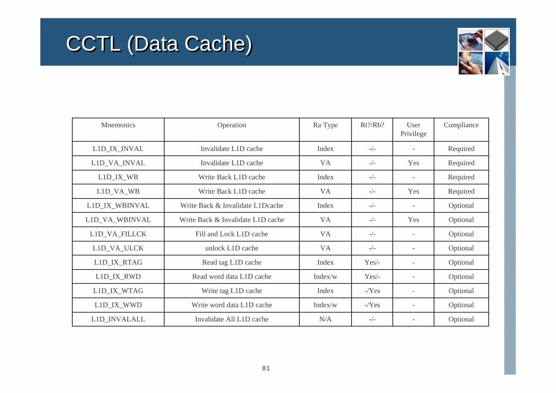
CCTL (Data Cache)CCTL (Data Cache)
Optional--/-N/AInvalidate All L1D cacheL1D_INVALALL
Optional--/YesIndex/wWrite word data L1D cacheL1D_IX_WWD
Optional--/YesIndexWrite tag L1D cacheL1D_IX_WTAG
Optional-Yes/-Index/wRead word data L1D cacheL1D_IX_RWD
Optional-Yes/-IndexRead tag L1D cacheL1D_IX_RTAG
Optional--/-VAunlock L1D cacheL1D_VA_ULCK
Optional--/-VAFill and Lock L1D cacheL1D_VA_FILLCK
OptionalYes-/-VAWrite Back & Invalidate L1D cacheL1D_VA_WBINVAL
Optional--/-IndexWrite Back & Invalidate L1DcacheL1D_IX_WBINVAL
RequiredYes-/-VAWrite Back L1D cacheL1D_VA_WB
Required--/-IndexWrite Back L1D cacheL1D_IX_WB
RequiredYes-/-VAInvalidate L1D cacheL1D_VA_INVAL
Required--/-IndexInvalidate L1D cacheL1D_IX_INVAL
ComplianceUserPrivilege
Rt?/Rb?Ra TypeOperationMnemonics
82
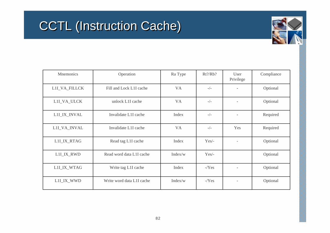
CCTL (Instruction Cache)CCTL (Instruction Cache)
Optional--/YesIndex/wWrite word data L1I cacheL1I_IX_WWD
Optional--/YesIndexWrite tag L1I cacheL1I_IX_WTAG
OptionalYes/-Index/wRead word data L1I cacheL1I_IX_RWD
Optional-Yes/-IndexRead tag L1I cacheL1I_IX_RTAG
RequiredYes-/-VAInvalidate L1I cacheL1I_VA_INVAL
Required--/-IndexInvalidate L1I cacheL1I_IX_INVAL
Optional--/-VAunlock L1I cacheL1I_VA_ULCK
Optional--/-VAFill and Lock L1I cacheL1I_VA_FILLCK
ComplianceUserPrivilege
Rt?/Rb?Ra TypeOperationMnemonics
83
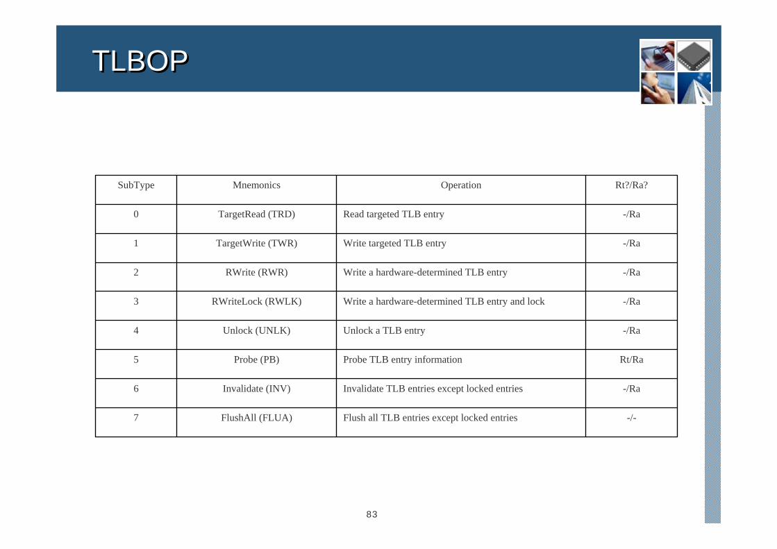
TLBOPTLBOP
-/-Flush all TLB entries except locked entriesFlushAll (FLUA)7
-/RaInvalidate TLB entries except locked entriesInvalidate (INV)6
Rt/RaProbe TLB entry informationProbe (PB)5
-/RaUnlock a TLB entryUnlock (UNLK)4
-/RaWrite a hardware-determined TLB entry and lockRWriteLock (RWLK)3
-/RaWrite a hardware-determined TLB entryRWrite (RWR)2
-/RaWrite targeted TLB entryTargetWrite (TWR)1
-/RaRead targeted TLB entryTargetRead (TRD)0
Rt?/Ra?OperationMnemonicsSubType
84
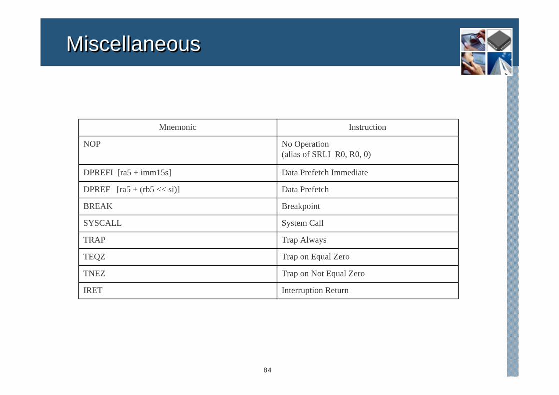
MiscellaneousMiscellaneous
Interruption ReturnIRET
Trap on Not Equal ZeroTNEZ
Trap on Equal ZeroTEQZ
Trap AlwaysTRAP
System CallSYSCALL
BreakpointBREAK
Data PrefetchDPREF [ra5 + (rb5 << si)]
Data Prefetch ImmediateDPREFI [ra5 + imm15s]
No Operation(alias of SRLI R0, R0, 0)
NOP
InstructionMnemonic
85
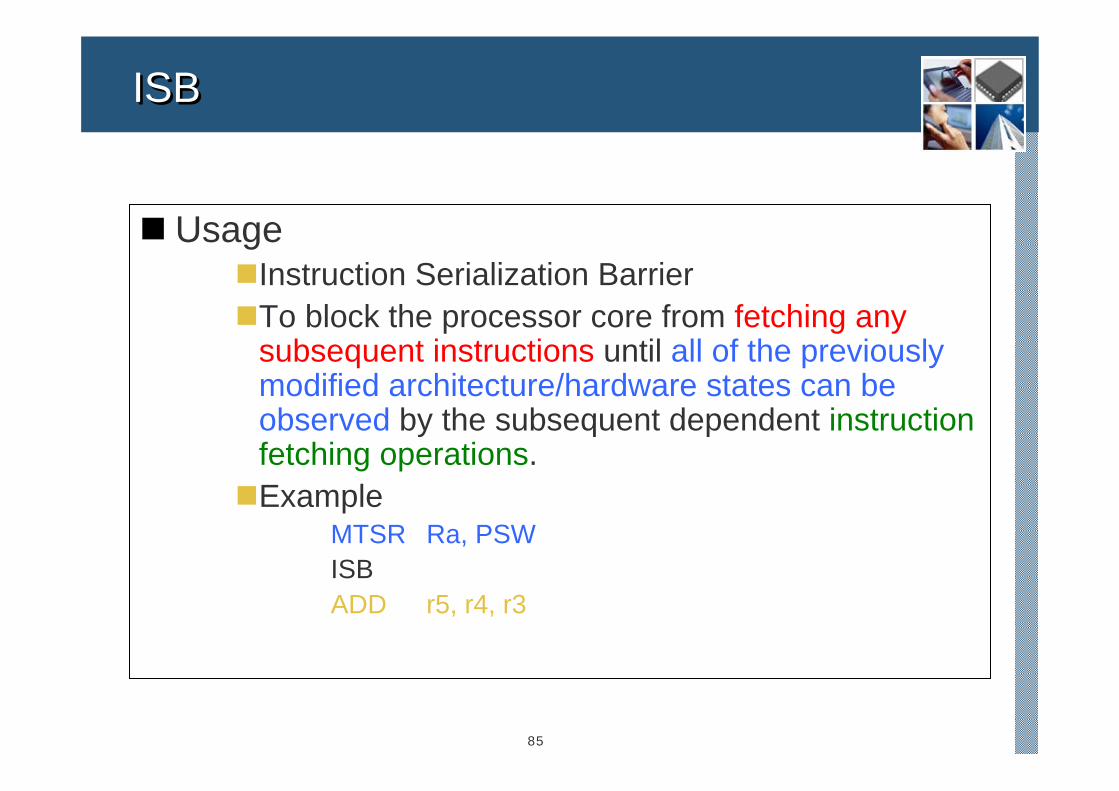
ISBISB
UsageInstruction Serialization BarrierTo block the processor core from fetching any subsequent instructions until all of the previously modified architecture/hardware states can be observed by the subsequent dependent instruction fetching operations.Example
MTSR Ra, PSWISBADD r5, r4, r3
86
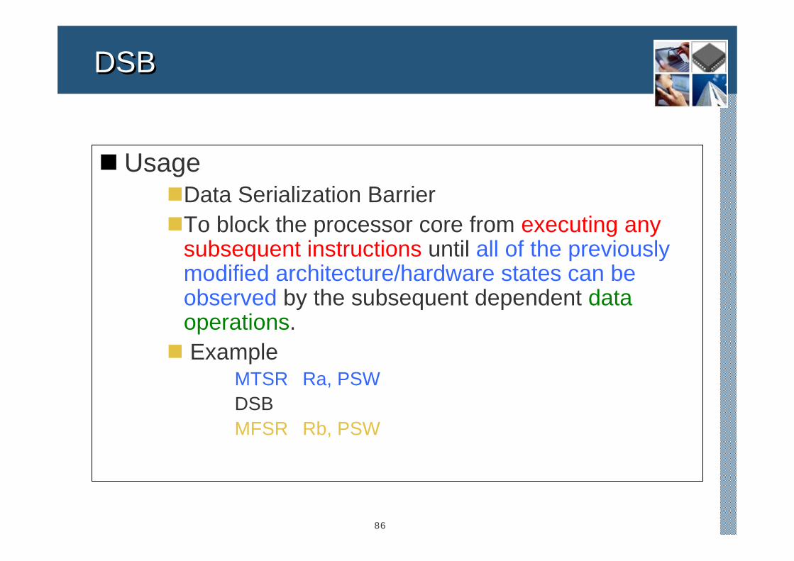
DSBDSB
UsageData Serialization BarrierTo block the processor core from executing any subsequent instructions until all of the previously modified architecture/hardware states can be observed by the subsequent dependent data operations.Example
MTSR Ra, PSWDSBMFSR Rb, PSW
87
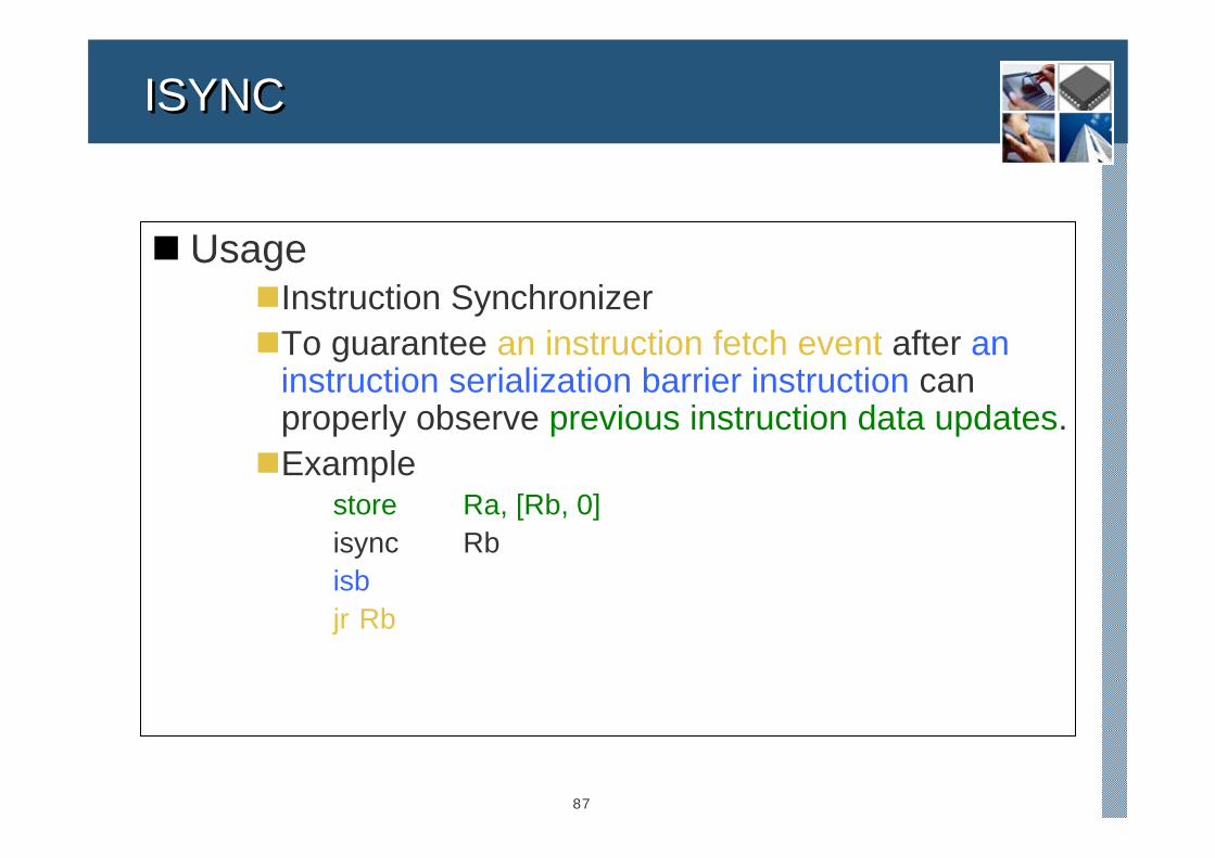
ISYNCISYNC
UsageInstruction SynchronizerTo guarantee an instruction fetch event after an instruction serialization barrier instruction can properly observe previous instruction data updates.Example
store Ra, [Rb, 0]isync Rbisbjr Rb
88
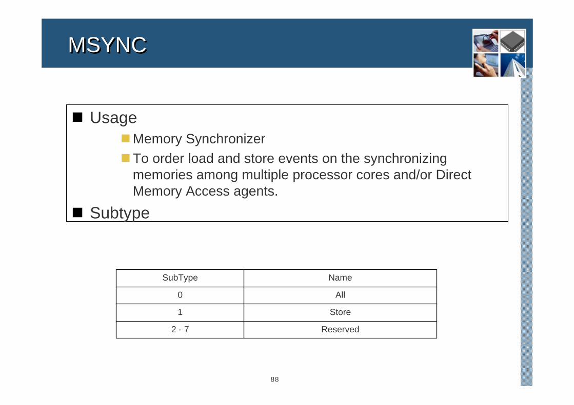
MSYNCMSYNC
UsageMemory SynchronizerTo order load and store events on the synchronizing memories among multiple processor cores and/or Direct Memory Access agents.
Subtype
Reserved2 - 7
Store1
All0
NameSubType
89
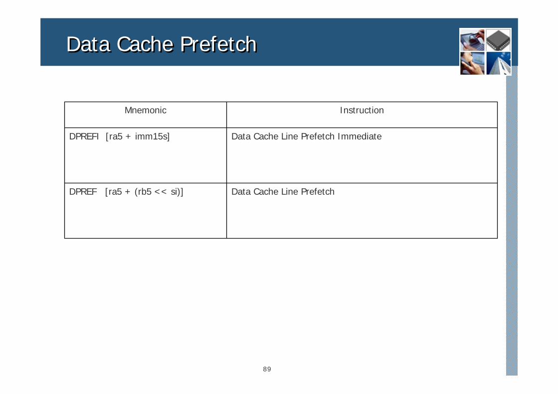
Data Cache PrefetchData Cache Prefetch
Data Cache Line PrefetchDPREF [ra5 + (rb5 << si)]
Data Cache Line Prefetch ImmediateDPREFI [ra5 + imm15s]
InstructionMnemonic
90
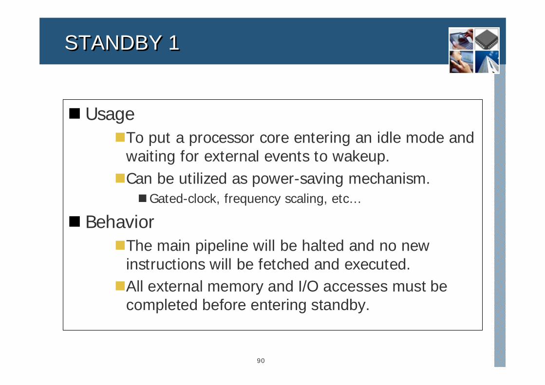
STANDBY 1STANDBY 1
UsageTo put a processor core entering an idle mode and waiting for external events to wakeup.Can be utilized as power-saving mechanism.
Gated-clock, frequency scaling, etc…
BehaviorThe main pipeline will be halted and no new instructions will be fetched and executed.All external memory and I/O accesses must be completed before entering standby.
91
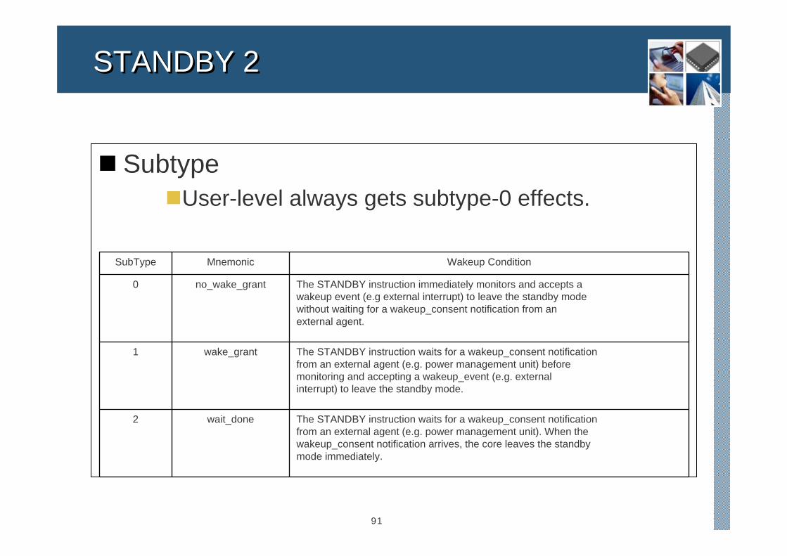
STANDBY 2STANDBY 2
SubtypeUser-level always gets subtype-0 effects.
The STANDBY instruction waits for a wakeup_consent notificationfrom an external agent (e.g. power management unit). When thewakeup_consent notification arrives, the core leaves the standbymode immediately.
wait_done2
The STANDBY instruction waits for a wakeup_consent notificationfrom an external agent (e.g. power management unit) beforemonitoring and accepting a wakeup_event (e.g. externalinterrupt) to leave the standby mode.
wake_grant1
The STANDBY instruction immediately monitors and accepts awakeup event (e.g external interrupt) to leave the standby modewithout waiting for a wakeup_consent notification from anexternal agent.
no_wake_grant0
Wakeup ConditionMnemonicSubType
92
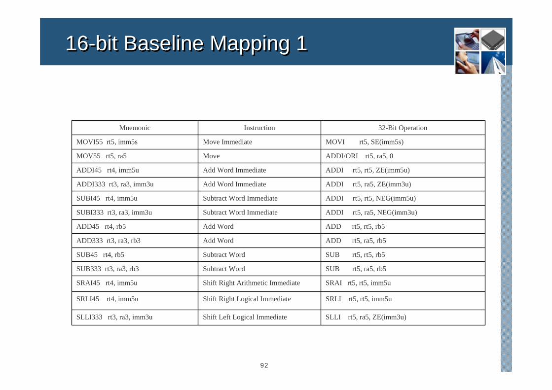
16-bit Baseline Mapping 116-bit Baseline Mapping 1
SLLI rt5, ra5, ZE(imm3u)Shift Left Logical ImmediateSLLI333 rt3, ra3, imm3u
SRLI rt5, rt5, imm5uShift Right Logical ImmediateSRLI45 rt4, imm5u
SRAI rt5, rt5, imm5uShift Right Arithmetic ImmediateSRAI45 rt4, imm5u
SUB rt5, ra5, rb5Subtract WordSUB333 rt3, ra3, rb3
SUB rt5, rt5, rb5Subtract WordSUB45 rt4, rb5
ADD rt5, ra5, rb5Add WordADD333 rt3, ra3, rb3
ADD rt5, rt5, rb5Add WordADD45 rt4, rb5
ADDI rt5, ra5, NEG(imm3u)Subtract Word ImmediateSUBI333 rt3, ra3, imm3u
ADDI rt5, rt5, NEG(imm5u)Subtract Word ImmediateSUBI45 rt4, imm5u
ADDI rt5, ra5, ZE(imm3u)Add Word ImmediateADDI333 rt3, ra3, imm3u
ADDI rt5, rt5, ZE(imm5u)Add Word ImmediateADDI45 rt4, imm5u
ADDI/ORI rt5, ra5, 0MoveMOV55 rt5, ra5
MOVI rt5, SE(imm5s)Move ImmediateMOVI55 rt5, imm5s
32-Bit OperationInstructionMnemonic
93
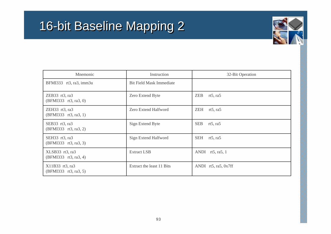
16-bit Baseline Mapping 216-bit Baseline Mapping 2
ANDI rt5, ra5, 0x7ffExtract the least 11 BitsX11B33 rt3, ra3(BFMI333 rt3, ra3, 5)
ANDI rt5, ra5, 1Extract LSBXLSB33 rt3, ra3(BFMI333 rt3, ra3, 4)
SEH rt5, ra5Sign Extend HalfwordSEH33 rt3, ra3(BFMI333 rt3, ra3, 3)
SEB rt5, ra5Sign Extend ByteSEB33 rt3, ra3(BFMI333 rt3, ra3, 2)
ZEH rt5, ra5Zero Extend HalfwordZEH33 rt3, ra3(BFMI333 rt3, ra3, 1)
ZEB rt5, ra5Zero Extend ByteZEB33 rt3, ra3(BFMI333 rt3, ra3, 0)
Bit Field Mask ImmediateBFMI333 rt3, ra3, imm3u
32-Bit OperationInstructionMnemonic
94
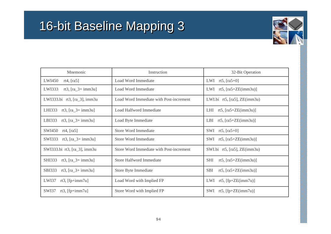
16-bit Baseline Mapping 316-bit Baseline Mapping 3
SBI rt5, [ra5+ZE(imm3u)]Store Byte ImmediateSBI333 rt3, [ra_3+ imm3u]
LWI rt5, [fp+ZE(imm7u)] Load Word with Implied FP LWI37 rt3, [fp+imm7u]
SWI rt5, [fp+ZE(imm7u)] Store Word with Implied FP SWI37 rt3, [fp+imm7u]
SHI rt5, [ra5+ZE(imm3u)]Store Halfword ImmediateSHI333 rt3, [ra_3+ imm3u]
SWI.bi rt5, [ra5], ZE(imm3u)Store Word Immediate with Post-incrementSWI333.bi rt3, [ra_3], imm3u
SWI rt5, [ra5+ZE(imm3u)]Store Word ImmediateSWI333 rt3, [ra_3+ imm3u]
SWI rt5, [ra5+0]Store Word ImmediateSWI450 rt4, [ra5]
LBI rt5, [ra5+ZE(imm3u)]Load Byte ImmediateLBI333 rt3, [ra_3+ imm3u]
LHI rt5, [ra5+ZE(imm3u)]Load Halfword ImmediateLHI333 rt3, [ra_3+ imm3u]
LWI.bi rt5, [ra5], ZE(imm3u)Load Word Immediate with Post-incrementLWI333.bi rt3, [ra_3], imm3u
LWI rt5, [ra5+ZE(imm3u)]Load Word ImmediateLWI333 rt3, [ra_3+ imm3u]
LWI rt5, [ra5+0]Load Word ImmediateLWI450 rt4, [ra5]
32-Bit OperationInstructionMnemonic
95
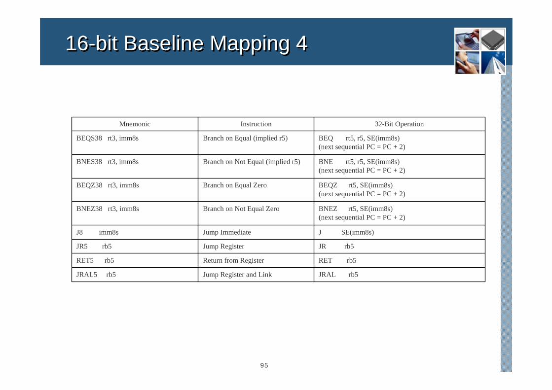
16-bit Baseline Mapping 416-bit Baseline Mapping 4
JRAL rb5Jump Register and LinkJRAL5 rb5
RET rb5Return from RegisterRET5 rb5
JR rb5Jump RegisterJR5 rb5
J SE(imm8s)Jump ImmediateJ8 imm8s
BNEZ rt5, SE(imm8s)(next sequential PC = PC + 2)
Branch on Not Equal ZeroBNEZ38 rt3, imm8s
BEQZ rt5, SE(imm8s)(next sequential PC = PC + 2)
Branch on Equal ZeroBEQZ38 rt3, imm8s
BNE rt5, r5, SE(imm8s)(next sequential PC = PC + 2)
Branch on Not Equal (implied r5)BNES38 rt3, imm8s
BEQ rt5, r5, SE(imm8s)(next sequential PC = PC + 2)
Branch on Equal (implied r5)BEQS38 rt3, imm8s
32-Bit OperationInstructionMnemonic
96
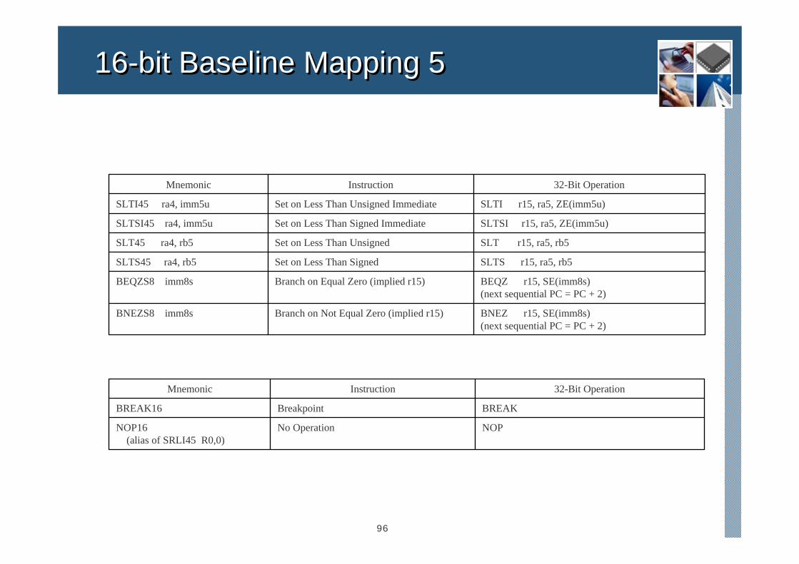
16-bit Baseline Mapping 516-bit Baseline Mapping 5
BNEZ r15, SE(imm8s)(next sequential PC = PC + 2)
Branch on Not Equal Zero (implied r15)BNEZS8 imm8s
BEQZ r15, SE(imm8s)(next sequential PC = PC + 2)
Branch on Equal Zero (implied r15)BEQZS8 imm8s
SLTS r15, ra5, rb5Set on Less Than SignedSLTS45 ra4, rb5
SLT r15, ra5, rb5Set on Less Than UnsignedSLT45 ra4, rb5
SLTSI r15, ra5, ZE(imm5u)Set on Less Than Signed ImmediateSLTSI45 ra4, imm5u
SLTI r15, ra5, ZE(imm5u)Set on Less Than Unsigned ImmediateSLTI45 ra4, imm5u
32-Bit OperationInstructionMnemonic
NOPNo OperationNOP16(alias of SRLI45 R0,0)
BREAKBreakpointBREAK16
32-Bit OperationInstructionMnemonic
97
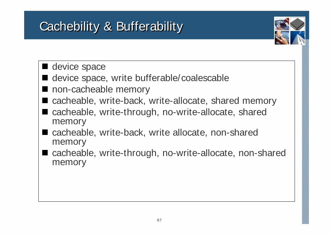
Cachebility & BufferabilityCachebility & Bufferability
device spacedevice space, write bufferable/coalescablenon-cacheable memorycacheable, write-back, write-allocate, shared memorycacheable, write-through, no-write-allocate, shared memorycacheable, write-back, write allocate, non-shared memorycacheable, write-through, no-write-allocate, non-shared memory
98
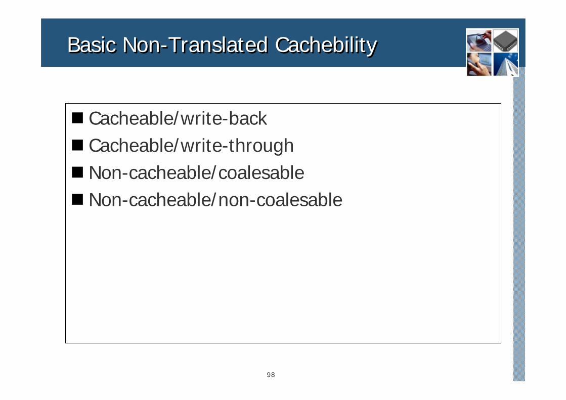
Basic Non-Translated CachebilityBasic Non-Translated Cachebility
Cacheable/write-backCacheable/write-throughNon-cacheable/coalesableNon-cacheable/non-coalesable
99
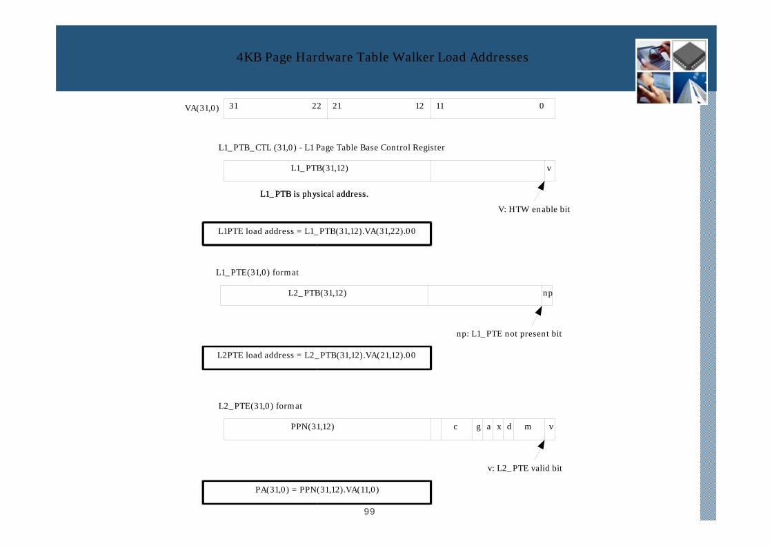
4KB Page Hardware Table Walker Load Addresses
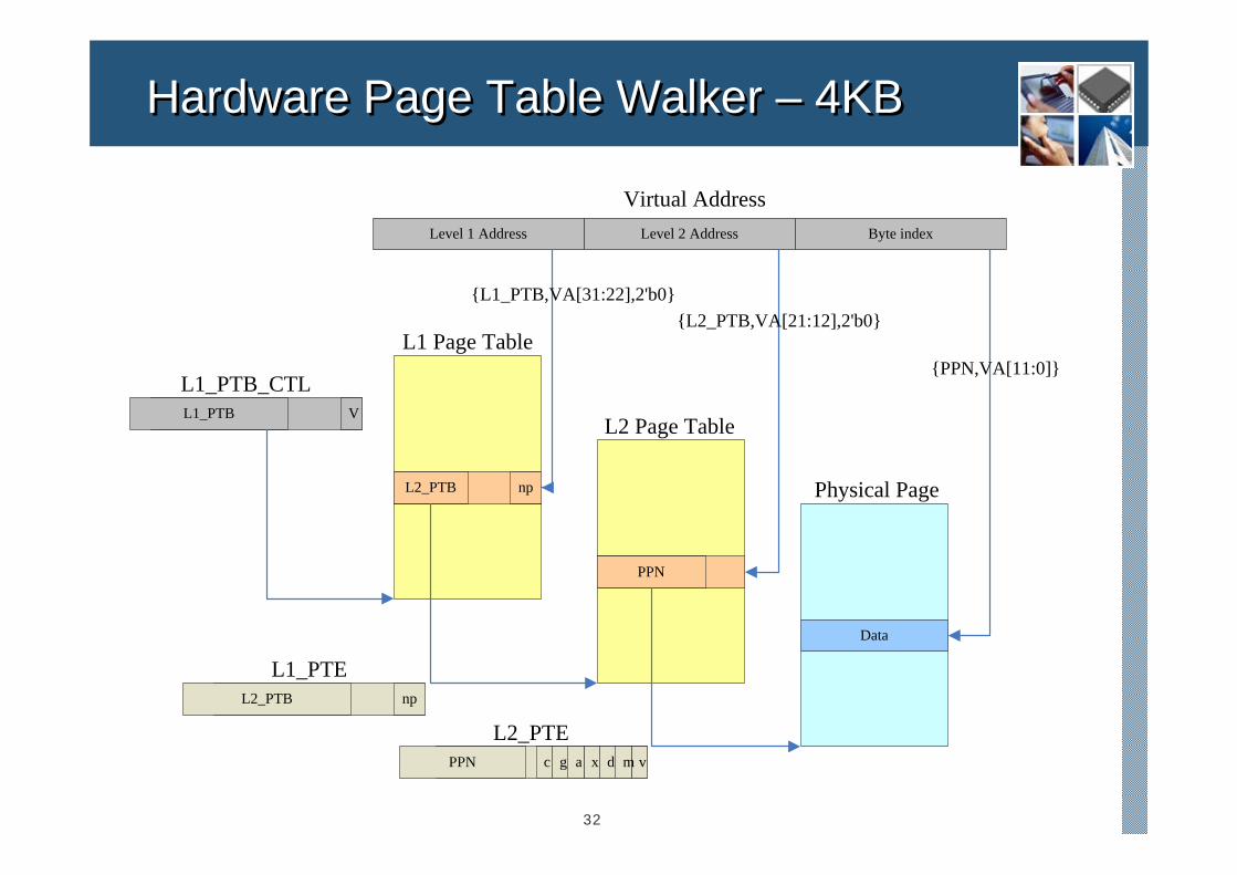
VA(31,0) 31 22 21 12 11 0
L1_PTB_CTL (31,0) - L1 Page Table Base Control Register
L1_PTB(31,12) v
V: HTW enable bit
L1PTE load address = L1_PTB(31,12).VA(31,22).00
L1_PTE(31,0) format
L2_PTB(31,12) np
np: L1_PTE not present bit
L1_PTB is physical address.
L2PTE load address = L2_PTB(31,12).VA(21,12).00
L1_PTB is physical address.
L2_PTE(31,0) format
PPN(31,12) v
v: L2_PTE valid bit
mda xgc
PA(31,0) = PPN(31,12).VA(11,0)
100
Priority of InterruptionsPriority of Interruptions
101
Priority of Interruptions (Conti…)Priority of Interruptions (Conti…)
102
Basic Counting EventsBasic Counting Events
uDTLB missuDTLB access15
uITLB missuITLB access14
stores completed (SMW count as 1)loads completed (LMW count as 1)13
exceptions takentaken interrupt12
-CCTL instruction11
ld-after-st conflict replaysISB/DSB instruction10
failed SCWSCW instruction9
16-bit instructionsNOP instruction8
multiply instsJAL/JRAL insts7
immeidate J insts (exclude JAL)JR (non-RET) inst6
RET mispredictRET inst5
prefetch with $ hitprefetch insts4
taken conditional branch mispredicttaken conditional branches3
conditional branch mispredictconditional branch2
completed instructions1
total cycles0
C2C1SEL
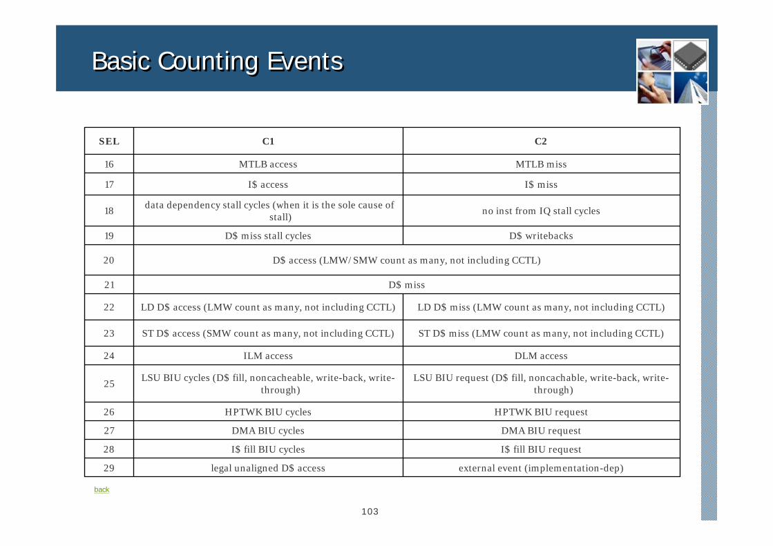
103
Basic Counting EventsBasic Counting Events
external event (implementation-dep)legal unaligned D$ access29
I$ fill BIU requestI$ fill BIU cycles28
DMA BIU requestDMA BIU cycles27
HPTWK BIU requestHPTWK BIU cycles26
LSU BIU request (D$ fill, noncachable, write-back, write-through)
LSU BIU cycles (D$ fill, noncacheable, write-back, write-through)
25
DLM accessILM access24
ST D$ miss (LMW count as many, not including CCTL)ST D$ access (SMW count as many, not including CCTL)23
LD D$ miss (LMW count as many, not including CCTL)LD D$ access (LMW count as many, not including CCTL)22
D$ miss21
D$ access (LMW/SMW count as many, not including CCTL)20
D$ writebacksD$ miss stall cycles19
no inst from IQ stall cyclesdata dependency stall cycles (when it is the sole cause of
stall)18
I$ missI$ access17
MTLB missMTLB access16
C2C1SEL
back
104
Performance Extension InstructionPerformance Extension Instruction
105
String Extension InstructionString Extension Instruction
106
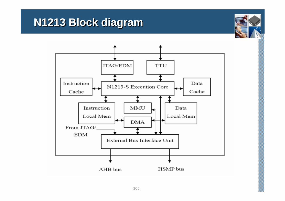
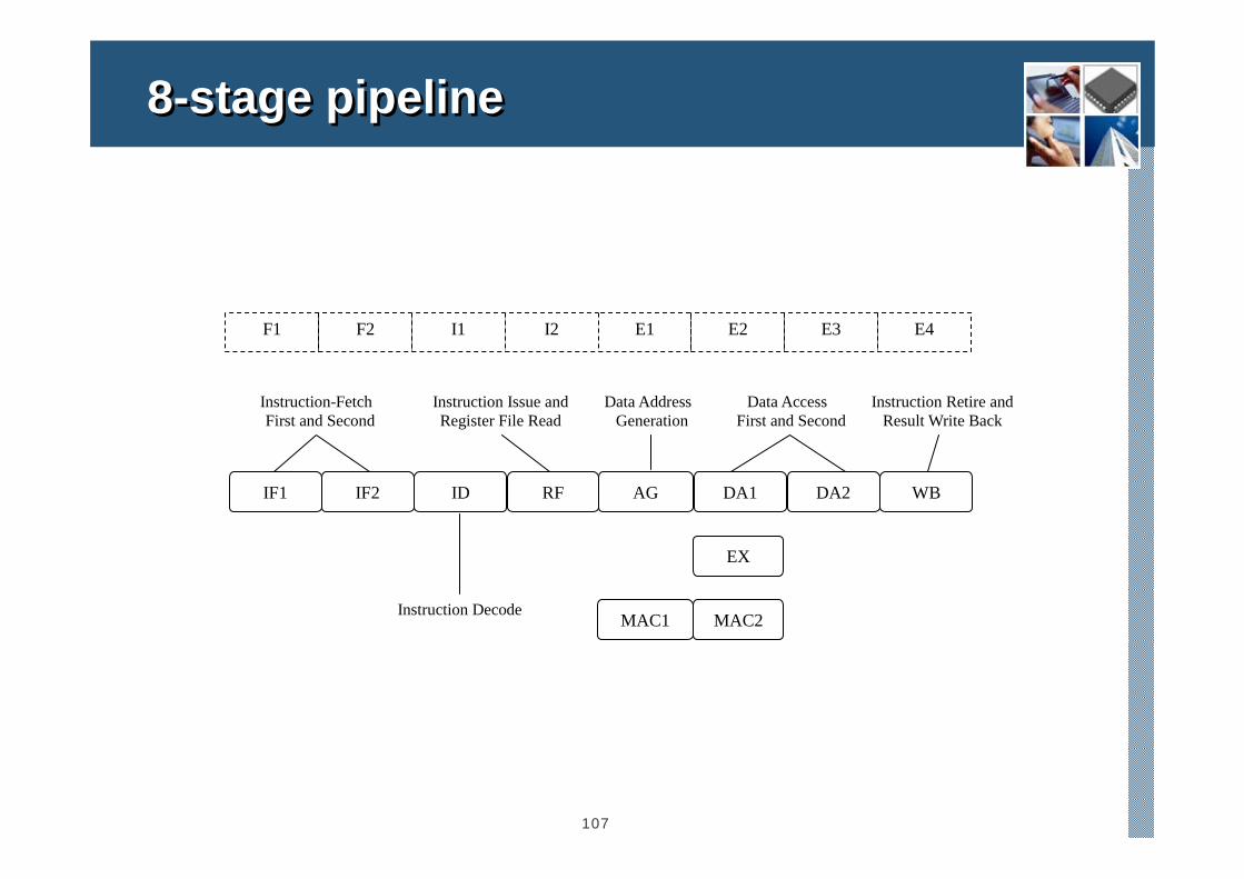
N1213 Block diagramN1213 Block diagram
107
RF
EX
IF1 IF2 ID DA1 DA2 WB
Instruction-Fetch First and Second
Instruction Decode
Instruction Issue andRegister File Read
AG
Instruction Retire andResult Write Back
Data Access First and Second
Data Address Generation
F1 F2 I1 I2 E1 E2 E3 E4
MAC1 MAC2
8-stage pipeline8-stage pipeline

108
4KB Page Hardware Table Walker Load Addresses
VA(31,0) 31 22 21 12 11 0
L1_PTB_CTL (31,0) - L1 Page Table Base Control Register
L1_PTB(31,12) v
V: HTW enable bit
L1PTE load address = L1_PTB(31,12).VA(31,22).00
L1_PTE(31,0) format
L2_PTB(31,12) np
np: L1_PTE not present bit
L1_PTB is physical address.
L2PTE load address = L2_PTB(31,12).VA(21,12).00
L1_PTB is physical address.
L2_PTE(31,0) format
PPN(31,12) v
v: L2_PTE valid bit
mda xgc
PA(31,0) = PPN(31,12).VA(11,0)

Thank You!!!Thank You!!!