Embed Size (px)
Citation preview
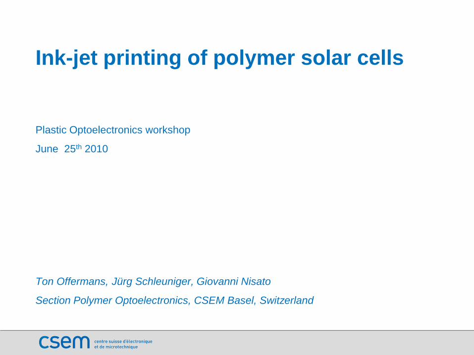
Ink-jet printing of polymer solar cells
Plastic Optoelectronics workshop
June 25th 2010
Ton Offermans, Jürg Schleuniger, Giovanni Nisato
Section Polymer Optoelectronics, CSEM Basel, Switzerland
Plastic Optoelectronics workshop June 25th 2010 | T. Offermans | Page 1
Outline
• CSEM
o Group Polymer Optoelectronics
• Inkjet printing polymer solar cells
o Novel low bandgap polymer
o Solvent mixtures
o Obtaining good uniformity
o Efficient inkjet printed devices
Plastic Optoelectronics workshop June 25th 2010 | T. Offermans | Page 2
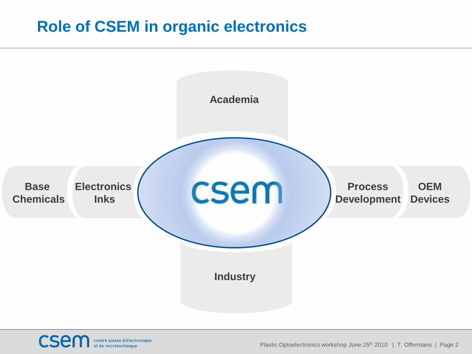
Role of CSEM in organic electronics
Electronics
Inks
Base
Chemicals
OEM
Devices
Process
Development
Academia
Industry
Plastic Optoelectronics workshop June 25th 2010 | T. Offermans | Page 3
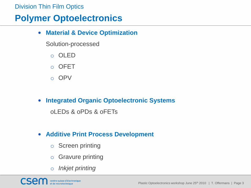
Division Thin Film Optics
Polymer Optoelectronics
• Material & Device Optimization
Solution-processed
o OLED
o OFET
o OPV
• Integrated Organic Optoelectronic Systems
oLEDs & oPDs & oFETs
• Additive Print Process Development
o Screen printing
o Gravure printing
o Inkjet printing
Plastic Optoelectronics workshop June 25th 2010 | T. Offermans | Page 4
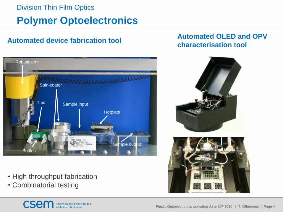
Division Thin Film Optics
Polymer Optoelectronics
Spin-coater
Sample input
Hotplate
Tips
Sample output
Bottles
Robotic arm
Automated device fabrication tool
• High throughput fabrication
• Combinatorial testing
Automated OLED and OPV
characterisation tool
Plastic Optoelectronics workshop June 25th 2010 | T. Offermans | Page 5
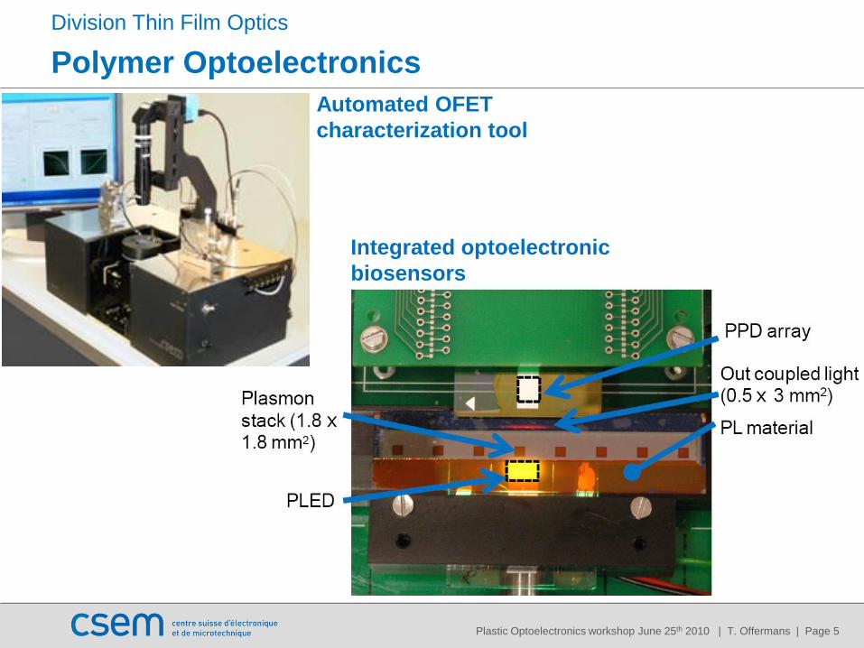
Automated OFET
characterization tool
Division Thin Film Optics
Polymer Optoelectronics
Integrated optoelectronic
biosensors
Plastic Optoelectronics workshop June 25th 2010 | T. Offermans | Page 6
Inkjet Printed OPV
Plastic Optoelectronics workshop June 25th 2010 | T. Offermans | Page 7
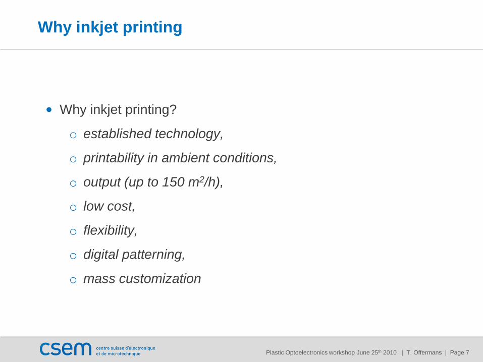
Why inkjet printing
• Why inkjet printing?
o established technology,
o printability in ambient conditions,
o output (up to 150 m2/h),
o low cost,
o flexibility,
o digital patterning,
o mass customization
Plastic Optoelectronics workshop June 25th 2010 | T. Offermans | Page 8
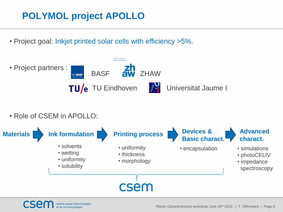
POLYMOL project APOLLO
Materials Ink formulation Printing process Devices &
Basic charact.• solvents
• wetting
• uniformity
• solubility
• uniformity
• thickness
• morphology
• simulations
• photoCELIV
• impedance
spectroscopy
Advanced
charact.
• Project goal: Inkjet printed solar cells with efficiency >5%.
• Role of CSEM in APOLLO:
BASF ZHAW
TU Eindhoven Universitat Jaume I
• Project partners :
• encapsulation
Plastic Optoelectronics workshop June 25th 2010 | T. Offermans | Page 9
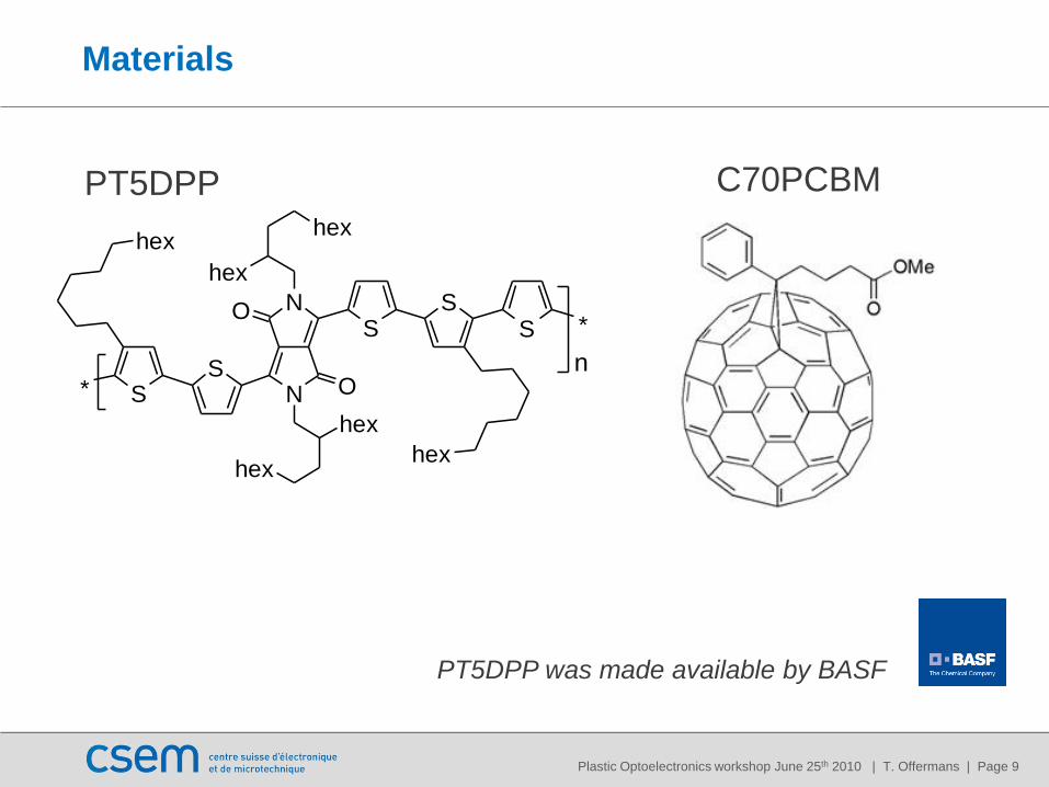
Materials
N
N
O
O
S
S
S
S
hex
hex
hex
hexhex
hex
S *
n
*
PT5DPP
PT5DPP was made available by BASF
C70PCBM
Plastic Optoelectronics workshop June 25th 2010 | T. Offermans | Page 10
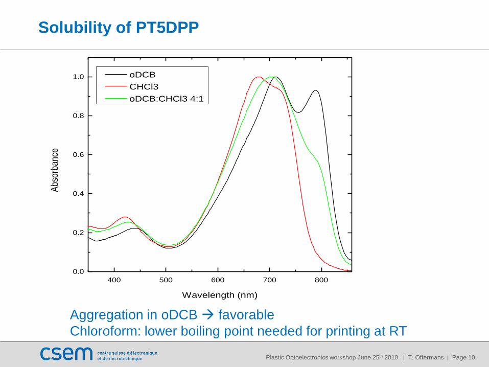
Solubility of PT5DPP
Aggregation in oDCB favorable
Chloroform: lower boiling point needed for printing at RT
400 500 600 700 800
0.0
0.2
0.4
0.6
0.8
1.0
Abs
orba
nce
Wavelength (nm)
oDCB
CHCl3
oDCB:CHCl3 4:1
Plastic Optoelectronics workshop June 25th 2010 | T. Offermans | Page 11
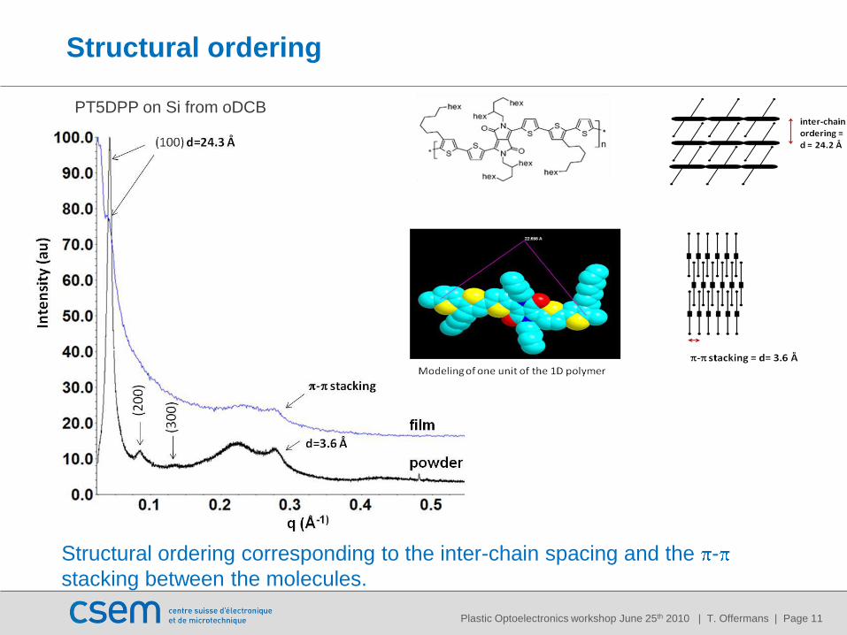
Structural ordering
Structural ordering corresponding to the inter-chain spacing and the -
stacking between the molecules.
PT5DPP on Si from oDCB
Plastic Optoelectronics workshop June 25th 2010 | T. Offermans | Page 12
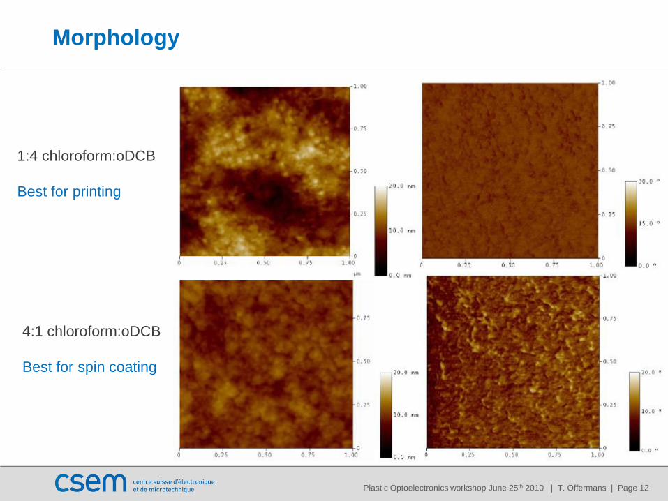
Morphology
1:4 chloroform:oDCB
Best for printing
4:1 chloroform:oDCB
Best for spin coating
Plastic Optoelectronics workshop June 25th 2010 | T. Offermans | Page 13
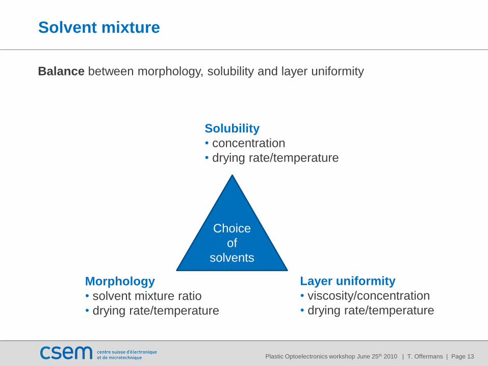
Solvent mixture
Morphology
• solvent mixture ratio
• drying rate/temperature
Solubility
• concentration
• drying rate/temperature
Layer uniformity
• viscosity/concentration
• drying rate/temperature
Choice
of
solvents
Balance between morphology, solubility and layer uniformity
Plastic Optoelectronics workshop June 25th 2010 | T. Offermans | Page 14
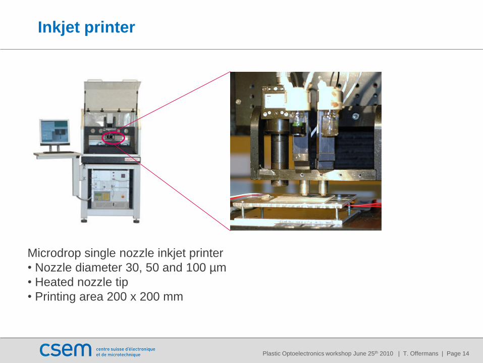
Inkjet printer
Microdrop single nozzle inkjet printer
• Nozzle diameter 30, 50 and 100 µm
• Heated nozzle tip
• Printing area 200 x 200 mm
Plastic Optoelectronics workshop June 25th 2010 | T. Offermans | Page 15
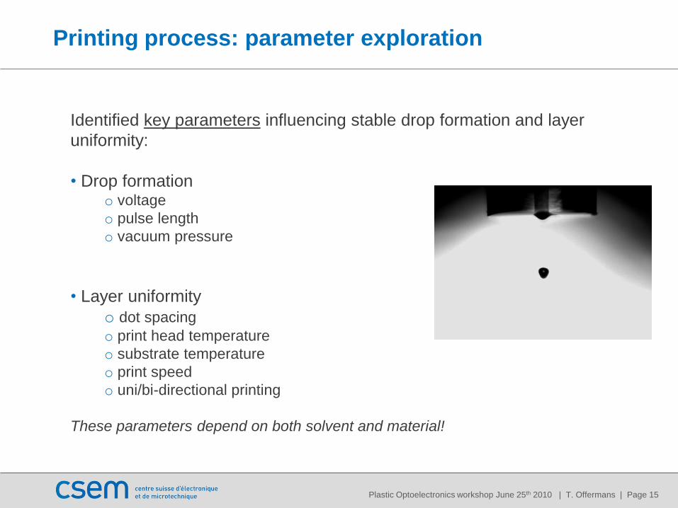
Printing process: parameter exploration
Identified key parameters influencing stable drop formation and layer
uniformity:
• Drop formationo voltage
o pulse length
o vacuum pressure
• Layer uniformity
o dot spacing
o print head temperature
o substrate temperature
o print speed
o uni/bi-directional printing
These parameters depend on both solvent and material!
Plastic Optoelectronics workshop June 25th 2010 | T. Offermans | Page 16
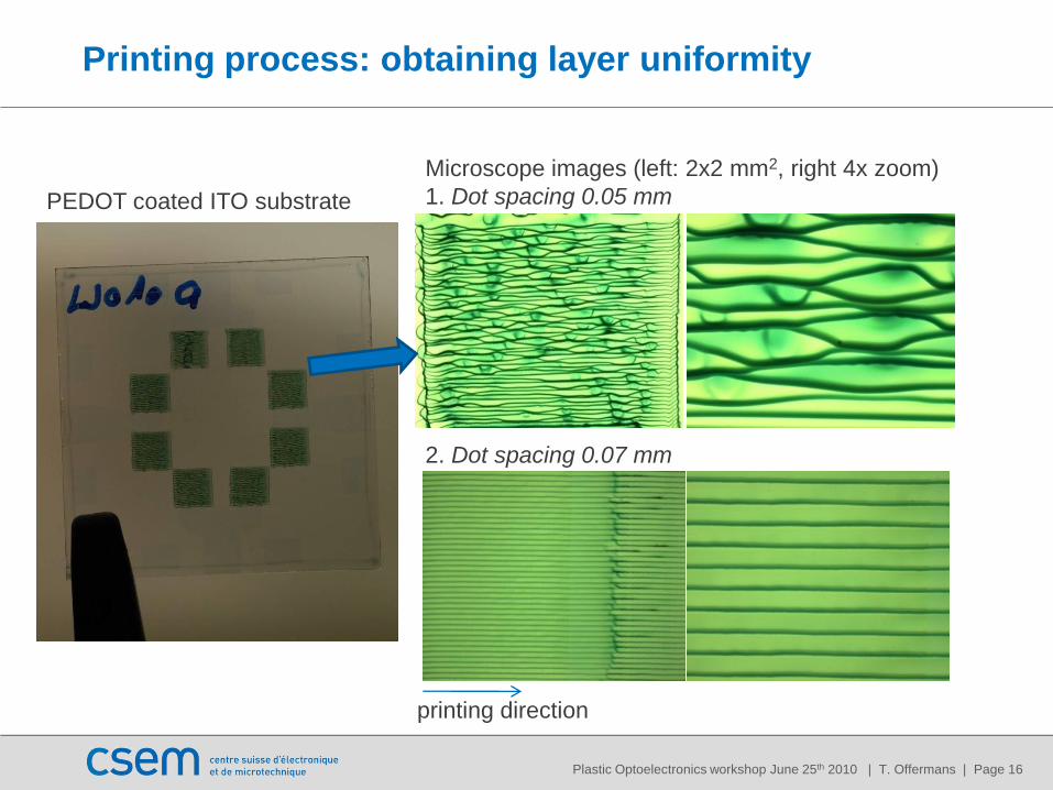
Printing process: obtaining layer uniformity
Microscope images (left: 2x2 mm2, right 4x zoom)
1. Dot spacing 0.05 mm
2. Dot spacing 0.07 mm
PEDOT coated ITO substrate
printing direction
Plastic Optoelectronics workshop June 25th 2010 | T. Offermans | Page 17
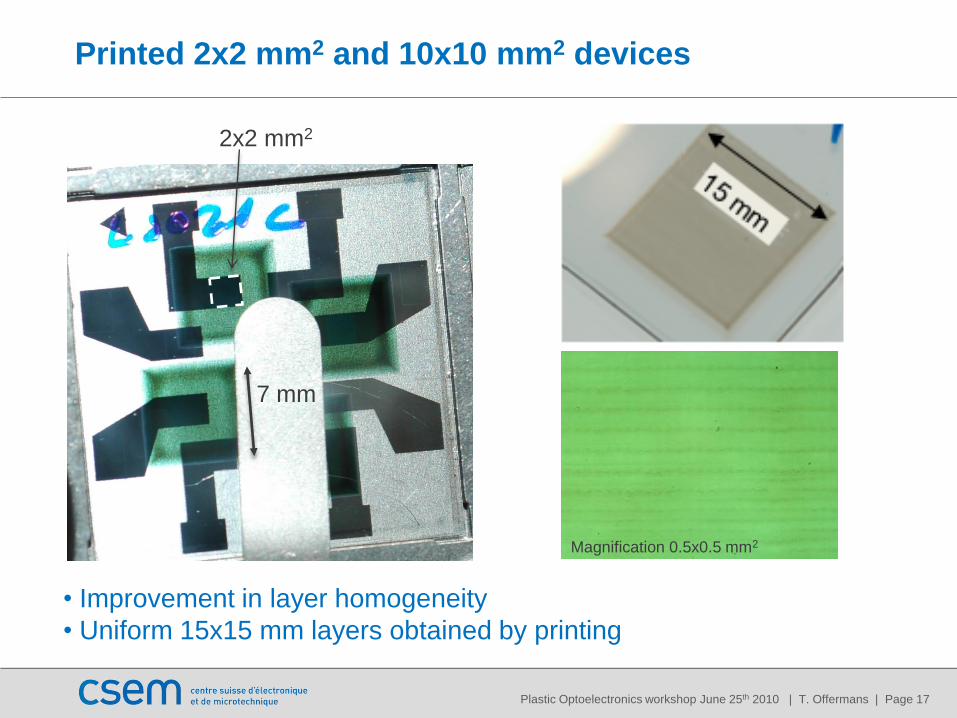
Printed 2x2 mm2 and 10x10 mm2 devices
• Improvement in layer homogeneity
• Uniform 15x15 mm layers obtained by printing
2x2 mm2
Magnification 0.5x0.5 mm2
7 mm
Plastic Optoelectronics workshop June 25th 2010 | T. Offermans | Page 18
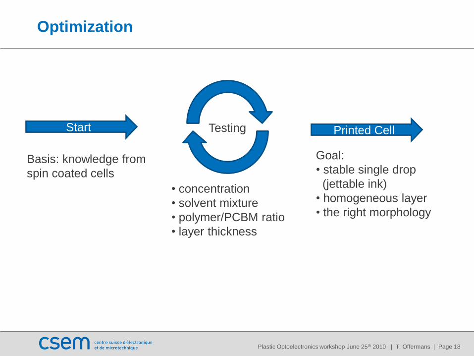
Optimization
Start
Basis: knowledge from
spin coated cells
Goal:
• stable single drop
(jettable ink)
• homogeneous layer
• the right morphology
Printed CellTesting
• concentration
• solvent mixture
• polymer/PCBM ratio
• layer thickness
Plastic Optoelectronics workshop June 25th 2010 | T. Offermans | Page 19
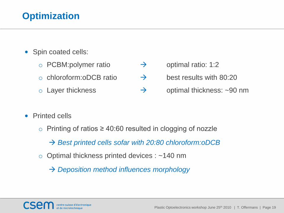
Optimization
• Spin coated cells:
o PCBM:polymer ratio optimal ratio: 1:2
o chloroform:oDCB ratio best results with 80:20
o Layer thickness optimal thickness: ~90 nm
• Printed cells
o Printing of ratios ≥ 40:60 resulted in clogging of nozzle
Best printed cells sofar with 20:80 chloroform:oDCB
o Optimal thickness printed devices : ~140 nm
Deposition method influences morphology
Plastic Optoelectronics workshop June 25th 2010 | T. Offermans | Page 20
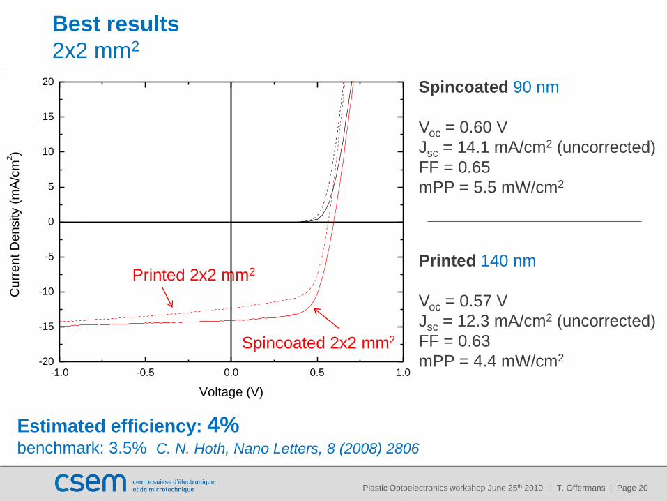
Best results
2x2 mm2
Spincoated 90 nm
Voc = 0.60 V
Jsc = 14.1 mA/cm2 (uncorrected)
FF = 0.65
mPP = 5.5 mW/cm2
Printed 140 nm
Voc = 0.57 V
Jsc = 12.3 mA/cm2 (uncorrected)
FF = 0.63
mPP = 4.4 mW/cm2
Spincoated 2x2 mm2
Printed 2x2 mm2
-1.0 -0.5 0.0 0.5 1.0-20
-15
-10
-5
0
5
10
15
20
Cu
rre
nt D
en
sity (
mA
/cm
2)
Voltage (V)
Estimated efficiency: 4% benchmark: 3.5% C. N. Hoth, Nano Letters, 8 (2008) 2806
Plastic Optoelectronics workshop June 25th 2010 | T. Offermans | Page 21
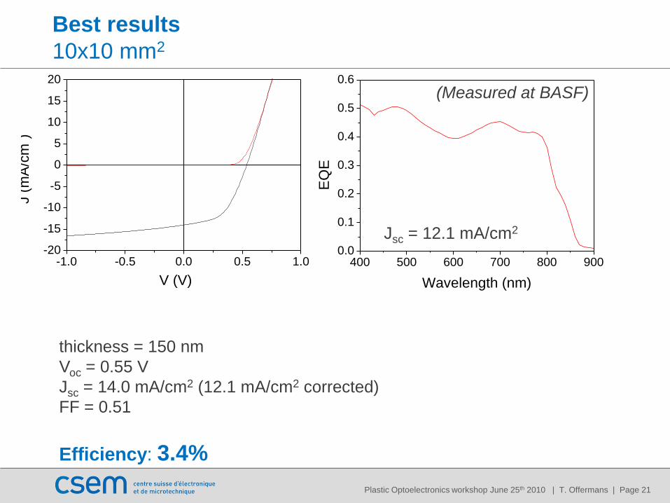
Best results
10x10 mm2
400 500 600 700 800 9000.0
0.1
0.2
0.3
0.4
0.5
0.6
EQ
E
Wavelength (nm)
-1.0 -0.5 0.0 0.5 1.0-20
-15
-10
-5
0
5
10
15
20
V (V)
J (
mA
/cm
2)
thickness = 150 nm
Voc = 0.55 V
Jsc = 14.0 mA/cm2 (12.1 mA/cm2 corrected)
FF = 0.51
Efficiency: 3.4%
(Measured at BASF)
Jsc = 12.1 mA/cm2
Plastic Optoelectronics workshop June 25th 2010 | T. Offermans | Page 22
Acknowledgements
• At CSEM:
• Basel: Jürg Schleuniger, Giovanni Nisato, Marek Chrapa, Guillaume Basset
• Neuchatel: Olha Sereda, Antonia Neels, Nicolas Blondiaux, Véronique Monnier
• APOLLO project partners :
• Funding from Swiss Federal Office of Energy
BASF ZHAW
TU Eindhoven Universitat Jaume I
Plastic Optoelectronics workshop June 25th 2010 | T. Offermans | Page 23
Take home messages
CSEM:
• is an R&D company working with universities and industry
• is developing processes and technologies, also for organic electronics
• has presented ink-jet printed solar cells with 4% efficiency
Thank you for your attention!