Embed Size (px)
Citation preview
Ink-Jet Printing of PLED Displays
After years of materials, hardware, and process development, the ink-jet printing of polymerlight-emitting-diode displays is on the verge of becoming a practical, commercial reality.
by Jonathan Halls
ELLOWING the first fortuitous observa-
tion of a faint green glow from a sample ofa polymer material by a team at CambridgeUniversity in 1989, Cambridge DisplayTechnology (CDT) was founded in 1992 todevelop this luminescence effect into a com-mercially viable emissive-display technology.Over the past 12 years, extensive work has
been done by CDT and other companies todevelop the performance - primarily effi-ciency, color, and stability - of polymer light-emitting-diode (PLED) technology to a level
at which the requirements of real applicationscan be met.
PLEDs are a very versatile technology,
which has the potential to be used for lighting,simple alphanumeric displays, and full-colorflat-panel displays (FPDs). While the life-times of red and green devices have been
acceptable for many applications for a numberof years now, the much shorter lifetime ofblue devices has prohibited their widespreaduse until recently. However, with an R&Dprogram on blue PLEDs delivering substantialimprovements in this area, and with the devel-opment of a range of new blue-emitting
Jonathan Halls is Strategic TechnologyPlanner at Cambridge Display Technology,Ltd., Bldg. 2020, Cambourne Business Park,Cambridgeshire CB3 6DW, u.K.; telephone+44-(0)-1954-713600,fax +44-(0)-1954-713620, e-mail:[email protected]. Theauthor thanks David Albertalli (Litrex Corp.),10hnAttard (Xaar), Linda Creigh (Spectra,Inc.), and Martin Fleuster and Nijs van derVaart (Philips)for useful discussions andassistance in the preparation of this article.
10 Infonnation Display 2/05
polymers, full-color PLED displays can nowbe used in a range of products. Moreover, thecontinual rapid progress in lifetime and stabil-ity means that more-challenging applications,such as TV, will probably be feasible in theforeseeable future.
However, in commercializing a new displaytechnology, device performance is only onepart of the story. Unless PLED displays canbe manufactured in a cost-effective way involumes high enough to satisfy the vastappetite of the display market, PLEDs willnever fulfill anything other than niche applica-tions.
SINGLERGB
PIXEL
One characteristic that is very interestingfrom a manufacturing perspective is thatPLED materials are solution-processable,unlike the vacuum-deposited materials usedto fabricate small-molecule-OLED displays.This brings with it a new set of challengesand opportunities. First, the coating anddeposition methods used to deposit solution-processable PLEDs are scalable to large sub-strate sizes. In contrast, the complexity, cost,relatively low material-utilization efficiency,and mask-registration issues associated withvacuum deposition present considerable diffi-culties in the application of small-molecule-
REDNOZZLE
DROPLET
DROPLETTRAJECTORYVECTOR
GREEN
BLUE
RED
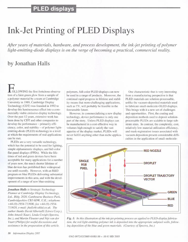
Fig. 1: In this illustration of the ink-Jet-printing process as applied to PLED-display fabrica-tion, the red-light-emitting-polymer ink is deposited into the appropriate subpixel wells, follow-ing deposition of the blue and green materials. (Courtesy of Spectra, Inc.)
0362-0972/02/2005-010$1.00 + .00 @ SID 2005
OLED-display production to large substrates.However, while vacuum-deposition systemsare common in the display industry, coatingwith light-emitting-polymer (LEP) semicon-ductors uses processes much more familiar tothe graphical printing industry.
This article will explore recent develop-ments in the manufacturing techniques, plant,and infrastructure that will enable PLEDs to
compete effectively with existing and otheremerging display technologies. It will also tryto predict when we can expect to see the firstfull-color PLED-display products on the mar-ket using these production technologies.
Existing Commercial ProductsUp to now, the commercialization ofPLEDshas occurred on a limited scale. The first
volume consumer product that incorporated aPLED display was the Philips Sensotecshaver, launched in 2002, which used a small
monochrome orange display with icons, fixedlegends, and a small alphanumeric panel toindicate battery-charge status and main-tenance requirements. This display was man-ufactured in Philips's PLED-display produc-tion plant in Heerlen, The Netherlands, usinga simple spin-coating process to deposit theLEP and hole-transport layers.
More recently, Philips launched the MagicMirror 639 mobile-telephone handset witha monochrome passive-matrix secondarydisplay behind a semi-transparent mirror that
forms part of the exterior case of the clamshelltelephone. Philips reports that the telephonehas been selling extremely well.
OSRAM Opto Semiconductors is currentlyshipping a range of small monochrome (pre-
dominantly green, orange, and yellow) PLEDdisplays manufactured at its facility inPenang, Malaysia. The displays are beingsold to OEM manufacturers for inclusion in a
range of electronic devices from point-of-saledisplays to high-end audio-mixing desks.Delta Electronics and RiTdisplay (bothlocated in Taiwan) are also manufacturing arange of simple passive-matrix alphanumericand graphic displays. What all of these dis-plays have in common is that they aremonochrome, manufactured by a simple spin-coating process, and are generally from 1 to 2in. on the diagonal.
Full-Color Ink-Jet PrintingIn order to make a full-color PLED FPD, anarray of individual red, green, and blue PLED
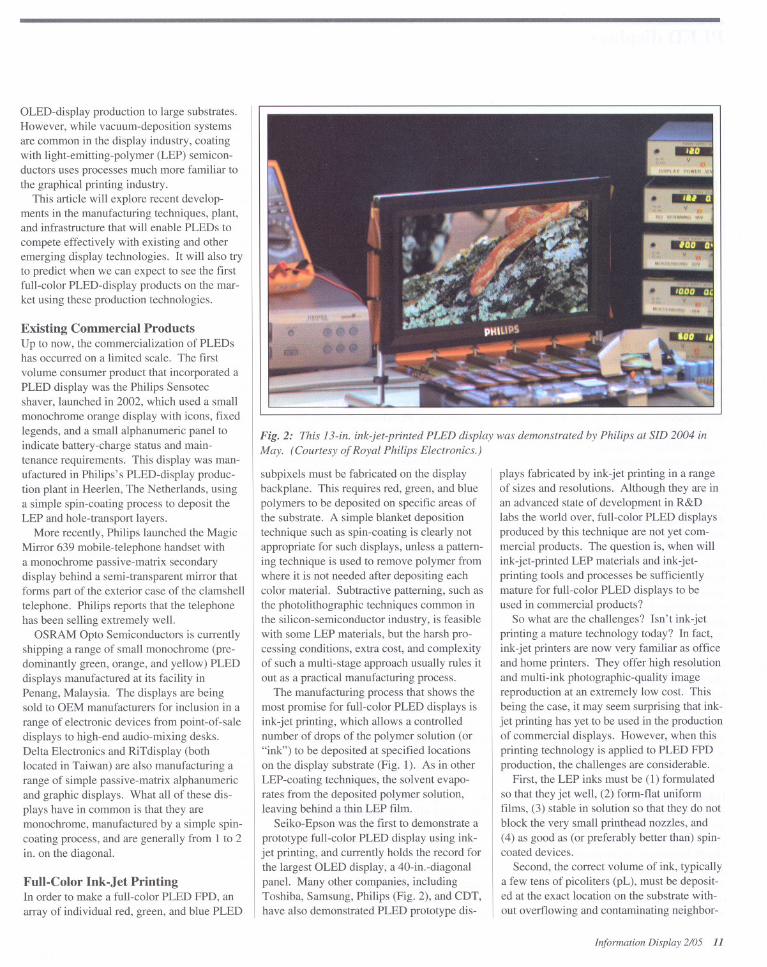
Fig. 2: This 13-in. ink-jet-printed PLED display was demonstrated by Philips at SID 2004 inMay. (Courtesy of Royal Philips Electronics.)
subpixels must be fabricated on the displaybackplane. This requires red, green, and bluepolymers to be deposited on specific areas of
the substrate. A simple blanket depositiontechnique such as spin-coating is clearly notappropriate for such displays, unless a pattern-ing technique is used to remove polymer fromwhere it is not needed after depositing each
color material. Subtractive patterning, such asthe photolithographic techniques common inthe silicon-semiconductor industry, is feasiblewith some LEP materials, but the harsh pro-
cessing conditions, extra cost, and complexityof such a multi-stage approach usually rules itout as a practical manufacturing process.
The manufacturing process that shows themost promise for full-color PLED displays isink-jet printing, which allows a controllednumber of drops of the polymer solution (or"ink") to be deposited at specified locationson the display substrate (Fig. 1). As in otherLEP-coating techniques, the solvent evapo-rates from the deposited polymer solution,leaving behind a thin LEP film.
Seiko-Epson was the first to demonstrate aprototype full-color PLED display using ink-jet printing, and currently holds the record for
the largest OLED display, a 40-in.-diagonalpanel. Many other companies, includingToshiba, Samsung, Philips (Fig. 2), and CDT,have also demonstrated PLED prototype dis-
plays fabricated by ink-jet printing in a rangeof sizes and resolutions. Although they are inan advanced state of development in R&Dlabs the world over, full-color PLED displaysproduced by this technique are not yet com-mercial products. The question is, when willink-jet-printed LEP materials and ink-jet-printing tools and processes be sufficientlymature for full-color PLED displays to beused in commercial products?
So what are the challenges? Isn't ink-jet
printing a mature technology today? In fact,ink-jet printers are now very familiar as officeand home printers. They offer high resolutionand multi-ink photographic-quality imagereproduction at an extremely low cost. Thisbeing the case, it may seem surprising that ink-jet printing has yet to be used in the production
of commercial displays. However, when thisprinting technology is applied to PLED FPDproduction, the challenges are considerable.
First, the LEP inks must be 0) formulated
so that they jet well, (2) form-flat uniformfilms, (3) stable in solution so that they do notblock the very small printhead nozzles, and(4) as good as (or preferably better than) spin-coated devices.
Second, the correct volume of ink, typically
a few tens of picoliters (pL), must be deposit-ed at the exact location on the substrate with-
out overflowing and contaminating neighbor-
Information Display 2/05 11
PLED displays
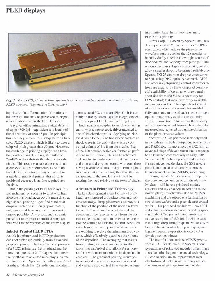
Fig. 3: The SX128printhead from Spectra is currently used by several companiesfor printingPLED displays. (Courtesy of Spectra, Inc.)
ing pixels of a different color. Variations inink-drop volume may be perceived as bright-ness variations across the PLED display.
A typical office printer has a pixel densityof up to 4800 dpi - equivalentto a localposi-tional accuracy of about 5 11m. In principle,this accuracy is more than adequate for a full-color PLED display, which is likely to have asubpixel pitch greater than 50 11m. However,the challenge in printing displays is to havethe printhead nozzles in register with the"wells" on the substrate that define the sub-
pixels. This requires an absolute positionalaccuracy of a few micrometers to be main-tained over the entire display surface. Fora standard graphical printer, this absolutepositional accuracy is neither required norfeasible.
But in the printing of PLED displays, it isnot sufficient for a printer to print with highabsolute positional accuracy; it must do so athigh speed, printing a specified number ofdrops in each of a million (approximately)red, green, and blue subpixels in as short atime as possible. Any errors, such as a mis-placed set of drops or an unfilled subpixel,will result in the rejection of the entire display.
Ink-Jet-Printed PLED FPDsAn ink-jet printer used in FPD production
does not differ substantially from a standardgraphical printer. The two main componentsof a PLED printer are the printhead and themotorized precision X-Y stage which movesthe printhead relative to the display substrate(or vice versa). Spectra, Inc., offers an SXl28printhead which has 128 individual nozzles in
12 Information Display 2/05
a row spaced 508 11mapart (Fig. 3). It is cur-rently in use by several system integrators whoare developing PLED manufacturing lines.
Each nozzle is coupled to an ink-containingcavity with a piezoelectric driver attached toone of the chamber walls. Applying an elec-trical pulse to the piezo transducer produces ashock wave in the cavity that ejects a con-trolled volume of ink from the nozzle. Each
of the 128 nozzles, which are formed as perfo-rations in the nozzle plate, can be activatedand deactivated individually, and can fire sev-eral thousand drops per second, with each drophaving a volume of about 10 pL. Printing intosubpixels that are closer together than the lin-ear spacing of the nozzles is achieved byrotating the head relative to the rows of pixels.
Advances in Printhead TechnologyThe key development areas for ink-jet print-heads are increased drop-placement and vol-ume accuracy. Drop-placement accuracy is afunction of the position of the nozzle relativeto the ink "wells" on the substrate and the
deviation of the drop trajectory from the nor-mal to the nozzle plate. In order to better con-trol the volume of LEP-ink solution depositedin each subpixel well, printhead developersare working to reduce the minimum drop vol-ume, which effectively quantizes the volume
of ink deposited. The averaging that resultsfrom printing a greater number of smallerdrops into a subpixel also allows for a more-uniform volume of material to be deposited ineach cell. The graphical printing industry'sincreasing demands for improved gray scaleand variable drop control have created a large
information base that is very relevant toPLED FPD printing.
Litrex Corp., followed by Spectra, Inc., hasdeveloped custom "drive per nozzle" (DPN)electronics, which allows the piezo drivewaveform sent to each of the 128 nozzles to
be individually tuned to allow tight control ofdrop volume and velocity from jet to jet. Thisnot only increases display uniformity, but alsoallows smaller drops to be printed reliably; theSpectra SXl28 can print drop volumes downto 5 pL using DPN-optimized control. DPNand other ink-jet-printing control implementa-tions are enabled by the widespread commer-cial availability of op-amps with extremelyshort rise times (80 V/sec is necessary forDPN control) that were previously availableonly in custom ICs. The rapid developmentof drop-visualization systems has enabledfully automatic tuning of each nozzle throughoptical image analysis of ink drops understrobe illumination. This allows the velocityand volume dispensed from each nozzle to bemeasured and adjusted through modificationof the piezo drive waveform.
Spectra's SXl28 printhead is widely usedin the industry in both pilot-production facilitiesand R&D labs. Its successor, the SX2, is in an
advanced stage of development and is expectedto be launched commercially in early 2005.While the SXl28 has a gold-plated electro-formed nickel nozzle plate, the SX2 nozzleplate is fabricated in silicon by microelec-tromechanical-system (MEMS) machining.
Taking this MEMS technology a step fur-ther, the next generation of printheads - theM-class - will have a printhead module(cavities and ink channels in addition to thenozzle plate) entirely fabricated by MEMSmachining and the subsequent lamination oftwo silicon wafers and a piezoelectric-crystalwafer. This printhead module will have 304individually addressable nozzles with a spac-ing of about 280 11m,allowing printing at anative resolution of 180 dpi. It will be capa-ble of high drop-firing frequencies; 40 kHz isbeing achieved routinely in prototypes, andhigher-frequency operation is expected asdevelopment continues.
The use of silicon and the MEMS processfor the SX2 nozzle plates in Spectra's newgenerations of printhead modules offers manymore benefits the previous metal technology.Silicon nozzles are an improvement overelectroformed nickel nozzles. They reducethe number of jet-trajectory and nozzle-
placement errors, allowing far more preciseand consistent deposition. Silicon nozzleplates can also be fabricated to a greater thick-ness, allowing far-better rigidity and dimen-sional stability, resulting in improved nozzlepositioning and jetting accuracy. The thinelectroformed nozzle plates are susceptible to
permanent bowing, which brings the row ofnozzles out of alignment.
The current technology has other weak-nesses as well. The thin gold coating of the
SX128 printhead provides chemical resistanceto the solvents used to dissolve LEP materials
and to the highly acidic PEDOT:PSS - thehole-transport material commonly used inPLED displays. The electroformed nozzleplate is typically 25 flm in thickness, and itssoft gold coating is easily damaged by abra-sion during maintenance. A thicker electro-formed layer would prevent acceptable dropformation and compromise the directionalaccuracy of the ejected drops. If the goldlayer is defective, the nozzle plate would bedamaged by the acidic inks, and jetting perfor-mance would be severely compromised,
requiring replacement of the entire printhead.Spectra, Inc., is just one of the companies
working to deliver next-generation printheads.Konica has developed a printhead capable ofdispensing drops in volumes down to 7 pL, afigure that can be reduced to 3 pL by utilizingDPN nozzle tuning. Xaar (Cambridge, U.K.)is developing a 1O00-nozzle printhead basedon their proprietary "Side Shooter" technology.Each nozzle will be individually tunable andcapable of variable-drop-size dispensing,based on a 3-pL sub-drop volume with eightor more levels of gray scale. The nozzle platewill have a parylene coating to protect it fromchemical corrosion, and precision construction
will deliver a drop-landing accuracy of less than5 flill at a l-mm substrate-printhead spacing.
The printhead will be specially designed tocope with the relatively high viscosity of LEPinks and will be capable of firing up to 8000full drops per second from each nozzle at avelocity of more than 6 m/sec. Xaar will alsointroduce the continuous recycling of inkthrough the channels, manifolds, and reservoirs,allowing removal of air bubbles and debris thatwould otherwise block nozzles or stop them
from firing. The printhead is projected to beavailable to system integrators by Q4 '05.
Advances in Ink-Jet PrintersA PLED-display printer integrates the print-
head described above with the substrate- and
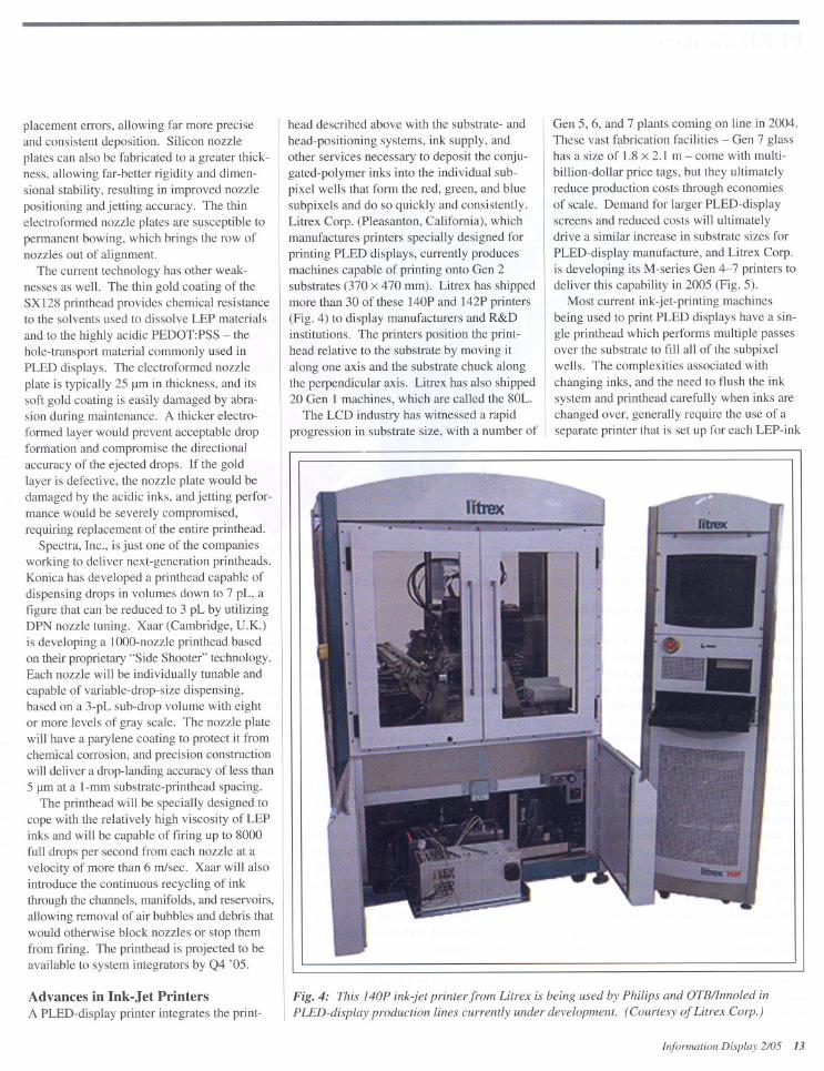
head-positioning systems, ink supply, andother services necessary to deposit the conju-gated-polymer inks into the individual sub-pixel wells that form the red, green, and bluesubpixels and do so quickly and consistently.Litrex Corp. (Pleasanton, California), whichmanufactures printers specially designed forprinting PLED displays, currently producesmachines capable of printing onto Gen 2substrates (370 x 470 mm). Litrex has shippedmore than 30 of these l40P and l42P printers
(Fig. 4) to display manufacturers and R&Dinstitutions. The printers position the print-head relative to the substrate by moving it
along one axis and the substrate chuck alongthe perpendicular axis. Litrex has also shipped20 Gen 1 machines, which are called the 80L.
The LCD industry has witnessed a rapidprogression in substrate size, with a number of
Gen 5, 6, and 7 plants coming on line in 2004.These vast fabrication facilities - Gen 7 glasshas a size of 1.8 x 2.1 m - come with multi-
billion-dollar price tags, but they ultimatelyreduce production costs through economiesof scale. Demand for larger PLED-displayscreens and reduced costs will ultimatelydrive a similar increase in substrate sizes for
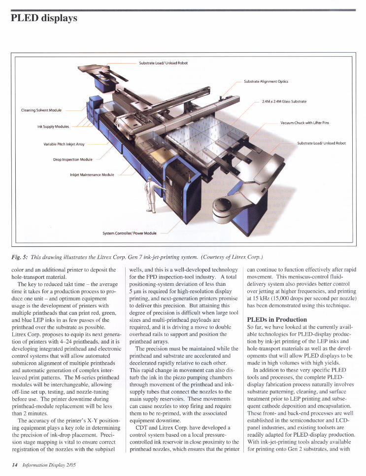
PLED-display manufacture, and Litrex Corp.is developing its M-series Gen 4-7 printers todeliver this capability in 2005 (Fig. 5).
Most current ink-jet-printing machines
being used to print PLED displays have a sin-gle printhead which performs multiple passesover the substrate to fill all of the subpixel
wells. The complexities associated withchanging inks, and the need to flush the inksystem and printhead carefully when inks arechanged over, generally require the use of aseparate printer that is set up for each LEP-ink
Fig. 4: This l40P ink-jet printer from Litrex is being used by Philips and OTB/lnnoled in
PLED-display production lines currently under development. (Courtesy of Litrex Corp.)
Information Display 2/05 13
PLED displays
Cleaning Solvent Module
Ink Supply Modules
Variable Pitch Inkjet Array
Drop Inspection Module
Inkjet Maintenance Module
Substrate Load! Unload Robot
System Controller! Power Module
Substrate Alignment Optics
204M x 204M Glass Substrate
Vacuum Chuck with Lifter Pins
Substrate Load! Unload Robot
Fig. 5: This drawing illustrates the Litrex Corp. Gen 7 ink-jet-printing system. (Courtesy of Litrex Corp.)
color and an additional printer to deposit thehole-transport material.
The key to reduced takt time - the averagetime it takes for a production process to pro-duce one unit - and optimum equipmentusage is the development of printers withmultiple printheads that can print red, green,and blue LEP inks in as few passes of theprinthead over the substrate as possible.Litrex Corp. proposes to equip its next genera-tion of printers with 4-24 printheads, and it isdeveloping integrated printhead and electroniccontrol systems that will allow automatedsubmicron alignment of multiple printheadsand automatic generation of complex inter-
leaved print patterns. The M-series printheadmodules will be interchangeable, allowingoff-line set up, testing, and nozzle-tuningbefore use. The printer downtime duringprinthead-module replacement will be lessthan 2 minutes.
The accuracy of the printer's X-Y position-ing equipment plays a key role in determiningthe precision of ink-drop placement. Preci-sion stage mapping is vital to ensure correctregistration of the nozzles with the subpixel
14 Information Display 2/05
wells, and this is a well-developed technologyfor the FPD inspection-tool industry. A total
positioning-system deviation of less than5 J.UIlis required for high-resolution displayprinting, and next-generation printers promiseto deliver this precision. But attaining thisdegree of precision is difficult when large toolsizes and multi-printhead payloads arerequired, and it is driving a move to doubleoverhead rails to support and position theprinthead arrays.
The precision must be maintained while theprinthead and substrate are accelerated and
decelerated rapidly relative to each other.This rapid change in movement can also dis-turb the ink in the piezo pumping chambersthrough movement of the printhead and ink-supply tubes that connect the nozzles to themain supply reservoirs. These movements
can cause nozzles to stop firing and requirethem to be re-primed, with the associatedequipment downtime.
CDT and Litrex Corp. have developed acontrol system based on a local pressure-
controlled ink reservoir in close proximity to theprinthead nozzles, which ensures that the printer
can continue to function effectively after rapidmovement. This meniscus-control fluid-
delivery system also provides better control
over jetting at higher frequencies, and printingat 15 kHz (15,000 drops per second per nozzle)has been demonstrated using this technique.
PLEDs in Production
So far, we have looked at the currently avail-able technologies for PLED-display produc-tion by ink-jet printing of the LEP inks and
hole-transport materials as well as the devel-opments that will allow PLED displays to bemade in high volumes with high yields.
In addition to these very specific PLEDtools and processes, the complete PLED-
display fabrication process naturally involvessubstrate patterning, cleaning, and surfacetreatment prior to LEP printing and subse-quent cathode deposition and encapsulation.These front- and back-end processes are wellestablished in the semiconductor and LCD-
panel industries, and existing toolsets arereadily adapted for PLED-display production.With ink-jet-printing tools already availablefor printing onto Gen 2 substrates, and with
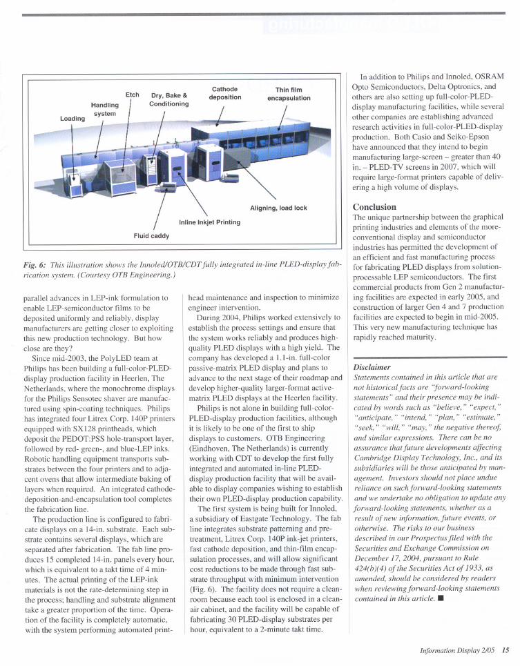
Etch
Fluid caddy
Aligning, load lock
Fig. 6: This illustration shows the InnolediOTB/CDTfully integrated in-line PLED-displayfab-rication system. (Courtesy OTB Engineering.)
parallel advances in LEP-ink fonnulation toenable LEP-semiconductor films to be
deposited uniformly and reliably, displaymanufacturers are getting closer to exploitingthis new production technology. But howclose are they?
Since mid-20m, the PolyLED team at
Philips has been building a full-color-PLED-display production facility in Heerlen, TheNetherlands, where the monochrome displays
for the Philips Sensotec shaver are manufac-tured using spin-coating techniques. Philipshas integrated four Litrex Corp. 140P printersequipped with SX128 printheads, whichdeposit the PEDOT:PSS hole-transport layer,followed by red- green-, and blue-LEP inks.
Robotic handling equipment transports sub-strates between the four printers and to adja-cent ovens that allow intennediate baking of
layers when required. An integrated cathode-deposition-and-encapsulation tool completesthe fabrication line.
The production line is configured to fabri-cate displays on a 14-in. substrate. Each sub-strate contains several displays, which are
separated after fabrication. The fab line pro-duces 15 completed 14-in. panels every hour,which is equivalent to a takt time of 4 min-utes. The actual printing of the LEP-inkmaterials is not the rate-detennining step in
the process; handling and substrate alignmenttake a greater proportion of the time. Opera-tion of the facility is completely automatic,with the system performing automated print-
head maintenance and inspection to minimizeengineer intervention.
During 2004, Philips worked extensively toestablish the process settings and ensure thatthe system works reliably and produces high-quality PLED displays with a high yield. Thecompany has developed a 1.I-in. full-colorpassive-matrix PLED display and plans toadvance to the next stage of their roadmap anddevelop higher-quality larger-fonnat active-matrix PLED displays at the Heerlen facility.
Philips is not alone in building full-color-PLED-display production facilities, althoughit is likely to be one of the first to shipdisplays to customers. OTB Engineering(Eindhoven, The Netherlands) is currently
working with CDT to develop the first fullyintegrated and automated in-line PLED-display production facility that will be avail-able to display companies wishing to establishtheir own PLED-display production capability.
The first system is being built for Innoled,a subsidiary of Eastgate Technology. The fabline integrates substrate patterning and pre-treatment, Litrex Corp. 140P ink-jet printers,
fast cathode deposition, and thin-film encap-sulation processes, and will allow significantcost reductions to be made through fast sub-strate throughput with minimum intervention(Fig. 6). The facility does not require a clean-room because each tool is enclosed in a clean-
air cabinet, and the facility will be capable offabricating 30 PLED-display substrates perhour, equivalent to a 2-minute takt time.
In addition to Philips and Innoled, OSRAMOpto Semiconductors, Delta Optronics, andothers are also setting up full-color-PLED-display manufacturing facilities, while severalother companies are establishing advancedresearch activities in full-color-PLED-display
production. Both Casio and Seiko-Epsonhave announced that they intend to beginmanufacturing large-screen - greater than 40in. - PLED-TV screens in 2007, which will
require large-format printers capable of deliv-ering a high volume of displays.
Conclusion
The unique partnership between the graphicalprinting industries and elements of the more-conventional display and semiconductorindustries has permitted the development ofan efficient and fast manufacturing processfor fabricating PLED displays from solution-
processable LEP semiconductors. The firstcommercial products from Gen 2 manufactur-ing facilities are expected in early 2005, andconstruction of larger Gen 4 and 7 productionfacilities are expected to begin in mid-2005.This very new manufacturing technique hasrapidly reached maturity.
DisclaimerStatements contained in this article that are
not historicalfacts are "forward-lookingstatements" and their presence may be indi-cated by words such as "believe," "expect,""anticipate," "intend," "plan," "estimate,""seek," "will," "may," the negative thereof,and similar expressions. There can be noassurance thatfuture developments affectingCambridge Display Technology, Inc., and itssubsidiaries will be those anticipated by man-agement. Investors should not place unduereliance on suchforward-looking statementsand we undertake no obligation to update anyforward-looking statements, whether as aresult of new information,future events, orotherwise. The risks to our business
described in our Prospectusfiled with theSecurities and Exchange Commission onDecember 17, 2004, pursuant to Rule424(b)(4) of the Securities Act of 1933, asamended, should be considered by readerswhen reviewingforward-looking statementscontained in this article. .
Information Display 2/05 15


![AN INSIGHT OF 3D PRINTING TECHNOLOGY IN … · Printing, Multi-Jet Modelling(MJM) and Multi-Jet-Printing or MJP by 3D Systems Corporation [19–21]. 2. Binder Jetting It is a prototype](https://img.pdfslide.us/doc/110x75/611967ea519aa857710692f4/an-insight-of-3d-printing-technology-in-printing-multi-jet-modellingmjm-and-multi-jet-printing.jpg)