Embed Size (px)
Citation preview
REL0.1 Page 1 of 64
iWave Systems Technologies Pvt. Ltd.
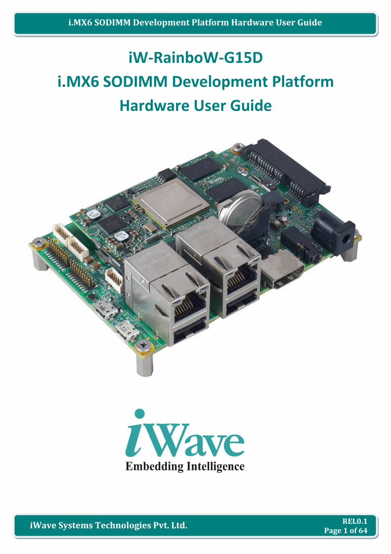
i.MX6 SODIMM Development Platform Hardware User Guide
iW-RainboW-G15D
i.MX6 SODIMM Development Platform
Hardware User Guide
REL0.1 Page 2 of 64
iWave Systems Technologies Pvt. Ltd.
i.MX6 SODIMM Development Platform Hardware User Guide
Document Revision History
Document Number iW-PREVD-UM-01-R2.1-REL0.1-Hardware_i.MX6_DevKit
Revision Date Change Description
0.1 29th Aug 2016 Intial draft release
PROPRIETARY NOTICE: This document contains proprietary material for the sole use of the intended recipient(s). Do
not read this document if you are not the intended recipient. Any review, use, distribution or disclosure by others is
strictly prohibited. If you are not the intended recipient (or authorized to receive for the recipient), you are hereby
notified that any disclosure, copying distribution or use of any of the information contained within this document is
STRICTLY PROHIBITED. Thank you. “iWave Systems Tech. Pvt. Ltd.”

REL0.1 Page 3 of 64
iWave Systems Technologies Pvt. Ltd.
i.MX6 SODIMM Development Platform Hardware User Guide
Disclaimer
iWave Systems reserves the right to change details in this publication including but not limited to any Product
specification without notice.
No warranty of accuracy is given concerning the contents of the information contained in this publication. To the
extent permitted by law no liability (including liability to any person by reason of negligence) will be accepted by
iWave Systems, its subsidiaries or employees for any direct or indirect loss or damage caused by omissions from or
inaccuracies in this document.
CPU and other major components used in this product may have several silicon errata associated with it. Under no
circumstances, iWave Systems shall be liable for the silicon errata and associated issues.
Trademarks
All registered trademarks, product names mentioned in this publication are the property of their respective owners
and used for identification purposes only.
Certification
iWave Systems Technologies Pvt. Ltd. is an ISO 9001:2015 Certified Company.
Warranty & RMA
Warranty support for Hardware: 1 Year from iWave or iWave's EMS partner.
For warranty terms, go through the below web link,
http://www.iwavesystems.com/support/warranty.html
For Return Merchandise Authorization (RMA), go through the below web link,
http://www.iwavesystems.com/support/rma.html
Technical Support
iWave Systems technical support team is committed to provide the best possible support for our customers so that
our Hardware and Software can be easily migrated and used.
For assistance, contact our Technical Support team at,
Email : [email protected]
Website : www.iwavesystems.com
Address : iWave Systems Technologies Pvt. Ltd.
# 7/B, 29th Main, BTM Layout 2nd Stage,
Bangalore, Karnataka,
India – 560076
REL0.1 Page 4 of 64
iWave Systems Technologies Pvt. Ltd.
i.MX6 SODIMM Development Platform Hardware User Guide
Table of Contents
1. INTRODUCTION ............................................................................................................................................ 8
1.1 Purpose ............................................................................................................................................................. 8
1.2 Overview ........................................................................................................................................................... 8
1.3 List of Acronyms ................................................................................................................................................ 8
1.4 Terminlogy Description ................................................................................................................................... 10
1.5 References ...................................................................................................................................................... 10
2. ARCHITECTURE AND DESIGN ....................................................................................................................... 11
2.1 i.MX6 SODIMM Carrier Board Block Diagram ................................................................................................. 11
2.2 i.MX6 SODIMM Carrier Board Features .......................................................................................................... 12
2.3 SODIMM Connector ........................................................................................................................................ 14
2.4 Serial Interface Features ................................................................................................................................. 26
2.4.1 Debug UART ................................................................................................................................................ 26
2.4.2 Data UART Header ...................................................................................................................................... 27
2.5 Communication Features ................................................................................................................................ 28
2.5.1 10/100/1000Mbps Ethernet ....................................................................................................................... 28
2.5.2 USB2.0 Device ............................................................................................................................................. 30
2.5.3 USB2.0 Host ................................................................................................................................................. 31
2.5.4 SDHC Port .................................................................................................................................................... 33
2.5.5 CAN Port ...................................................................................................................................................... 34
2.6 High Speed Interfaces ..................................................................................................................................... 35
2.6.1 Mini PCIe Port .............................................................................................................................................. 35
2.6.2 SATA Port..................................................................................................................................................... 38
2.7 Audio/Video Features ..................................................................................................................................... 40
2.7.1 Audio IN/OUT Jack ...................................................................................................................................... 40
2.7.2 4.3” RGB LCD with Touch ............................................................................................................................ 41
2.7.3 18BBP LVDS LCD with Resistive Touch ........................................................................................................ 44
2.7.4 HDMI Port.................................................................................................................................................... 47
2.8 Additional Features ......................................................................................................................................... 49
2.8.1 Boot Mode Switch ....................................................................................................................................... 49
2.8.2 Reset Switch ................................................................................................................................................ 50
2.8.3 JTAG Header ................................................................................................................................................ 51
2.8.4 RTC Coin cell Holder .................................................................................................................................... 53
2.9 Expansion Header ........................................................................................................................................... 54
2.10 GPIO Header .................................................................................................................................................... 56
2.11 Optional Features............................................................................................................................................ 57
2.11.1 RTC Controller ............................................................................................................................................. 57
3. TECHNICAL SPECIFICATION.......................................................................................................................... 58
3.1 Electrical Characteristics ................................................................................................................................. 58
3.1.1 Power Input Requirement ........................................................................................................................... 58
3.2 Environmental Characteristics ........................................................................................................................ 60
REL0.1 Page 5 of 64
iWave Systems Technologies Pvt. Ltd.
i.MX6 SODIMM Development Platform Hardware User Guide
3.2.1 Environmental Specification ........................................................................................................................ 60
3.2.2 RoHS Compliance ........................................................................................................................................ 60
3.2.3 Electrostatic Discharge ................................................................................................................................ 60
3.3 Mechanical Characteristics ............................................................................................................................. 61
3.3.1 i.MX6 SODIMM Carrier Board Mechanical Dimensions .............................................................................. 61
4. ORDERING INFORMATION .......................................................................................................................... 62
5. APPENDIX I ................................................................................................................................................. 63
5.1 Guidelines to insert the i.MX6 SODIMM SOM into Carrier Board .................................................................. 63
5.2 Guidelines to remove the i.MX6 SODIMM SOM from Carrier board ............................................................. 63
REL0.1 Page 6 of 64
iWave Systems Technologies Pvt. Ltd.
i.MX6 SODIMM Development Platform Hardware User Guide
List of Figures
Figure 1: i.MX6 SODIMM Carrier Board Block Diagram .................................................................................................. 11
Figure 2: SODIMM Connector ......................................................................................................................................... 14
Figure 3: Debug UART ..................................................................................................................................................... 26
Figure 4: Data UART Header ........................................................................................................................................... 27
Figure 5: 10/100/1000Mbps RJ45 MagJack .................................................................................................................... 28
Figure 6: USB2.0 Device Port .......................................................................................................................................... 30
Figure 7: USB 2.0 Host Ports ........................................................................................................................................... 31
Figure 8: Micro SD Connector ......................................................................................................................................... 33
Figure 9: CAN Header ...................................................................................................................................................... 34
Figure 10 : PCIe Slot ........................................................................................................................................................ 35
Figure 11 SATA Connector .............................................................................................................................................. 38
Figure 12: Audio IN/OUT Jack ......................................................................................................................................... 40
Figure 13: RGB LCD Connector ........................................................................................................................................ 41
Figure 14 LVDS LCD and Resistive Touch Connectors ..................................................................................................... 44
Figure 15 HDMI Connector ............................................................................................................................................. 47
Figure 16: Boot Switch .................................................................................................................................................... 49
Figure 17: Reset Switch ................................................................................................................................................... 50
Figure 18 JTAG Header .................................................................................................................................................... 51
Figure 19: RTC Coin Cell Holder ...................................................................................................................................... 53
Figure 20: Expansion Header .......................................................................................................................................... 54
Figure 21: GPIO Header................................................................................................................................................... 56
Figure 22: Power Jack...................................................................................................................................................... 58
Figure 23: Mechanical dimension of i.MX6 SODIMM Carrier Board .............................................................................. 61
Figure 24: Mechanical dimension of i.MX6 SODIMM Carrier Board - Side View............................................................ 61
Figure 25: i.MX6 SODIMM Module Insertion procedure ................................................................................................ 63
Figure 26: i.MX6 SODIMM Module Removal procedure ................................................................................................ 63
REL0.1 Page 7 of 64
iWave Systems Technologies Pvt. Ltd.
i.MX6 SODIMM Development Platform Hardware User Guide
List of Tables
Table 1: Acronyms & Abbreviations .................................................................................................................................. 8
Table 2: Terminology ...................................................................................................................................................... 10
Table 3: SODIMM Edge Connector Pin Out .................................................................................................................... 15
Table 4: Debug UART Connector Pin Out ........................................................................................................................ 26
Table 5: Data UART Header Pin Out ................................................................................................................................ 27
Table 6: RJ45 MagJack1 Pin Out ...................................................................................................................................... 29
Table 7: USB2.0 Device Connector Pin Out ..................................................................................................................... 30
Table 8: USB 2.0 Host 1 Connector (J5) Pin Out .............................................................................................................. 32
Table 9: USB 2.0 Host 2 Connector (J4) Pin Out .............................................................................................................. 32
Table 10: Micro SD Connector Pin Out ........................................................................................................................... 33
Table 11: CAN Header Pin Out ........................................................................................................................................ 34
Table 12 : PCIe Slot Pin Out ............................................................................................................................................. 35
Table 13 SATA Connector PinOut .................................................................................................................................... 38
Table 14: Audio In/Out Jack Pin Out ............................................................................................................................... 40
Table 15: 4.3” RGB LCD Connector Pin Out .................................................................................................................... 43
Table 16: LVDS LCD Connector Pin Out ........................................................................................................................... 45
Table 17: Resistive Touch Connector Pin Out ................................................................................................................. 45
Table 18: LVDS1 Backlight Connector Pin Out ................................................................................................................ 46
Table 19: HDMI Connector Pin Out ................................................................................................................................. 48
Table 20: Boot Mode Settings ......................................................................................................................................... 49
Table 21: JTAG Header .................................................................................................................................................... 51
Table 22: RTC Coin Cell Holder Pin Out ........................................................................................................................... 53
Table 23: Expansion Header Pin Out ............................................................................................................................... 55
Table 24: GPIO Header Pin Out ....................................................................................................................................... 57
Table 25: Power Jack Pin Out .......................................................................................................................................... 58
Table 26: Power Input Requirement ............................................................................................................................... 59
Table 27: Environmental Specification ........................................................................................................................... 60
Table 28: Orderable Product Part Numbers ................................................................................................................... 62

REL0.1 Page 8 of 64
iWave Systems Technologies Pvt. Ltd.
i.MX6 SODIMM Development Platform Hardware User Guide
1. INTRODUCTION
1.1 Purpose
i.MX6 SODIMM Development platform incorporates i.MX6 SODIMM SOM and Generic SODIMM Carrier board for
complete validation of i.MX6 SODIMM SOM functionality. This document is the Hardware User Guide for the i.MX6
SODIMM Carrier Board. This Guide provides detailed information on the overall design and usage of the SODIMM
Carrier Board from a Hardware Systems perspective. Complete information about the i.MX6 SODIMM SOM
hardware is explained in other document “i.MX6 SODIMM SOM-Hardware User Guide”.
1.2 Overview
iWave's i.MX6 SODIMM Development Board incorporates i.MX6 SODIMM SOM which is based on NXP's power
efficient i.MX6 ARM Cortex A9 processor and the SODIMM carrier board with optional 4.3" resistive display kit. The
development board can be used for quick prototyping of various applications targeted by the i.MX6 processor. With
the 100mmx72mm Pico ITX size, the kit is highly packed with all the necessary on-board connectors to validate the
i.MX6 CPU features.
1.3 List of Acronyms
The following acronyms will be used throughout this document.
Table 1: Acronyms & Abbreviations
Acronyms Abbreviations
A Ampere
ARM Advanced RISC Machine
BPP Bits Per Pixel
CAN Controller Area Network
CPU Central Processing unit
CSI Camera Sensor Interface
eCSPI Enhanced Configurable Serial Peripheral Interface
GPIO General Purpose Input Output
HDMI High Definition Multimedia Interface
I2C Inter-Integrated Circuit
I2S Integrated Interchip Sound
IC Integrated Circuit
I/O Input/ Output
JTAG Joint Test Action Group
LCD Liquid Crystal Display
LED Light Emitting Diode
LVDS Low Voltage Differential Signal
MB Mega Byte

REL0.1 Page 9 of 64
iWave Systems Technologies Pvt. Ltd.
i.MX6 SODIMM Development Platform Hardware User Guide
Acronyms Abbreviations
Mbps Mega Bits per sec
PCB Printed Circuit board
PCIe Peripheral Controller Interconnect Express
PWM Pulse Width Modulation
RGB Red Green Blue
RJ45 Registered Jack 45
RTC Real Time Clock
SAI Synchronous Audio Interface
SATA Serial Advanced Technology Attachment
SD Secure Digital
SODIMM Small Outline Dual in-line Memory Module
SOM System ON Module
SPI Serial Peripheral Interface
SSI Synchronous Serial Interface
UART Universal Asynchronous Receiver Transmitters
uSDHC Ultra-Secured Digital Host Controller
USB Universal Serial bus
USB OTG USB On The Go
V Voltage

REL0.1 Page 10 of 64
iWave Systems Technologies Pvt. Ltd.
i.MX6 SODIMM Development Platform Hardware User Guide
1.4 Terminlogy Description
In this document, wherever Signal Type is mentioned, below terminology is used.
Table 2: Terminology
Terminology Description
I Input Signal
O Output Signal
IO Bidirectional Input/output Signal
CMOS Complementary Metal Oxide Semiconductor Signal
DIFF Differential Signal
TMDS Transition-Minimized Differential Signalling
OD Open Drain Signal
OC Open Collector Signal
Analog Analog Signal
Power Power Pin
PU Pull Up
PD Pull Down
NA Not Applicable
NC Not Connected
Note: Signal Type does not include internal pull-ups or pull-downs implemented by the chip vendors and only includes
the pull-ups or pull-downs implemented on board.
1.5 References
i.MX6 SODIMM SOM Hardware User Guide
i.MX6 Datasheet

REL0.1 Page 11 of 64
iWave Systems Technologies Pvt. Ltd.
i.MX6 SODIMM Development Platform Hardware User Guide
2. ARCHITECTURE AND DESIGN
This section is designed to provide detailed information about the i.MX6 SODIMM Carrier Board Features and
Hardware architecture with high level block diagram. Also this section provides detailed information about each
block of i.MX6 SODIMM Carrier Board.
2.1 i.MX6 SODIMM Carrier Board Block Diagram
iW-RainboW-G15D - i.MX6 SODIMM Carrier Board Block Diagram
SODIMMPCB Edge Connector
(200Pin)
UART5
SDHC3
I2S
SATA
PCIe x 1
JTAG
3.3V Power IN
USB OTG1
RJ45 Mag Jack2
I2S Audio Codec
Audio In/Out Connector
I2S
Debug UARTUART to USB
Bridge
Debug USB Micro AB
Connector
UART2
Power Jack(5V)
3.3V Power Regulator
To On-Board Power Circuit & Peripherals
SDHC3 x 4bit
Mini PCIe Connector
CAN1CAN
Transceiver
SATA
PCIe x 1
JTAG Header JTAG
10/100/1000MbpsEthernet
USB HostUSB Host
RTC
Boot Mode, USB Select,ONOFF, RST
Control Switches
RTC Battery
18bpp RGB
PWM1PWM1
Generic RGB LCD Connector
18bpp RGB
HDMI
HDMI ConnectorHDMI
I2C1 I2C1
CAN1
UART5
RTC ControllerI2C1
2 Port USB HUB
UART1,UART4
SPI2
PWM2
GPIO’S
Expansion Header
Data UART1, Data UART4
SPI2
PWM2
GPIOs
LVDS LVDS0LVDS LCD
Connector and BKLT Conn
PWM3
I2C3Resistive Touch
Controller
I2C3 Resistive TP Connector
Capacitive TP ConnectorI2C3
GPIO Header
CAN2CAN2
22 Pin SATAConnector
Micro SDConnector
CAN Header
UART Header
USB OTG Micro AB Connector
RJ45 Mag Jack
USB TypeAConnector
PWM3
Figure 1: i.MX6 SODIMM Carrier Board Block Diagram
REL0.1 Page 12 of 64
iWave Systems Technologies Pvt. Ltd.
i.MX6 SODIMM Development Platform Hardware User Guide
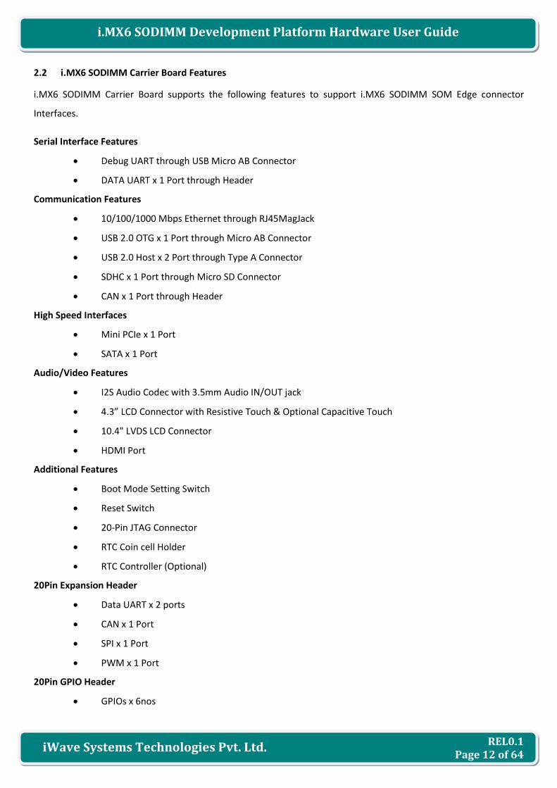
2.2 i.MX6 SODIMM Carrier Board Features
i.MX6 SODIMM Carrier Board supports the following features to support i.MX6 SODIMM SOM Edge connector
Interfaces.
Serial Interface Features
Debug UART through USB Micro AB Connector
DATA UART x 1 Port through Header
Communication Features
10/100/1000 Mbps Ethernet through RJ45MagJack
USB 2.0 OTG x 1 Port through Micro AB Connector
USB 2.0 Host x 2 Port through Type A Connector
SDHC x 1 Port through Micro SD Connector
CAN x 1 Port through Header
High Speed Interfaces
Mini PCIe x 1 Port
SATA x 1 Port
Audio/Video Features
I2S Audio Codec with 3.5mm Audio IN/OUT jack
4.3” LCD Connector with Resistive Touch & Optional Capacitive Touch
10.4" LVDS LCD Connector
HDMI Port
Additional Features
Boot Mode Setting Switch
Reset Switch
20-Pin JTAG Connector
RTC Coin cell Holder
RTC Controller (Optional)
20Pin Expansion Header
Data UART x 2 ports
CAN x 1 Port
SPI x 1 Port
PWM x 1 Port
20Pin GPIO Header
GPIOs x 6nos
REL0.1 Page 13 of 64
iWave Systems Technologies Pvt. Ltd.
i.MX6 SODIMM Development Platform Hardware User Guide
General Specification
Power Supply : 5V, 1A Power Input Jack
Form Factor : 100mm X 72mm Pico ITX.
REL0.1 Page 14 of 64
iWave Systems Technologies Pvt. Ltd.
i.MX6 SODIMM Development Platform Hardware User Guide
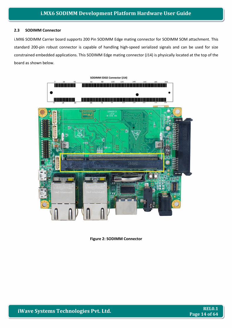
2.3 SODIMM Connector
i.MX6 SODIMM Carrier board supports 200 Pin SODIMM Edge mating connector for SODIMM SOM attachment. This
standard 200-pin robust connector is capable of handling high-speed serialized signals and can be used for size
constrained embedded applications. This SODIMM Edge mating connector (J14) is physically located at the top of the
board as shown below.
Figure 2: SODIMM Connector
REL0.1 Page 15 of 64
iWave Systems Technologies Pvt. Ltd.
i.MX6 SODIMM Development Platform Hardware User Guide
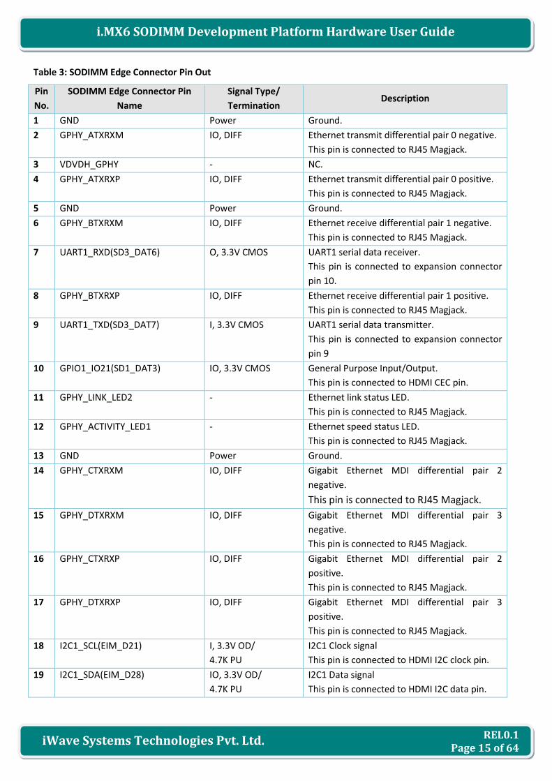
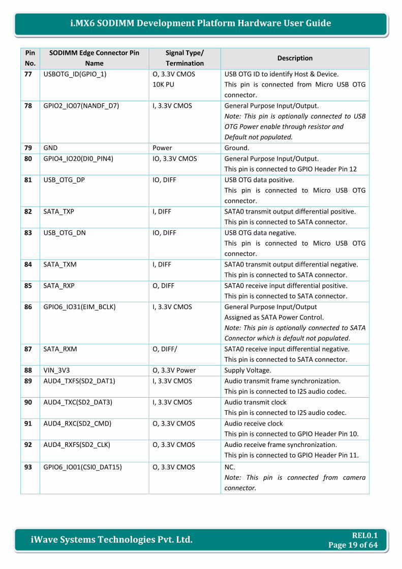
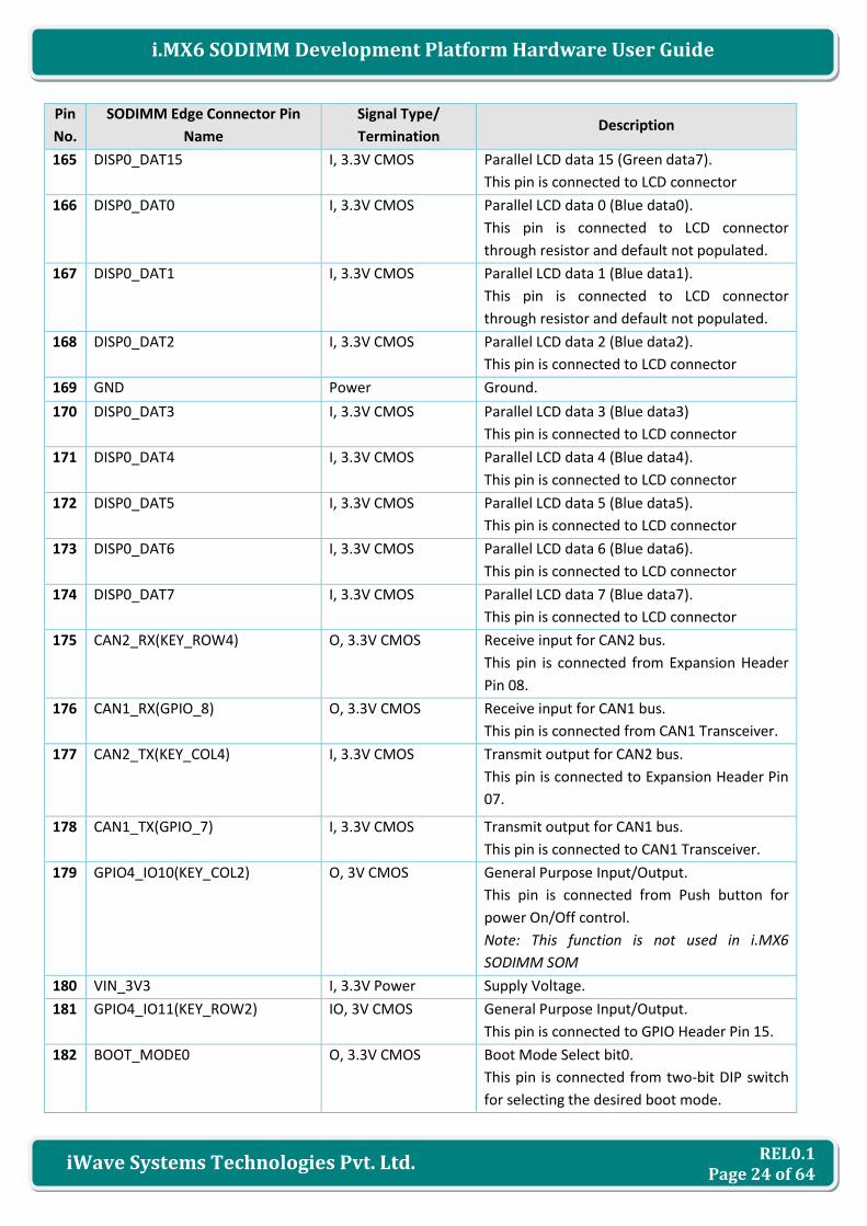
Table 3: SODIMM Edge Connector Pin Out
Pin
No.
SODIMM Edge Connector Pin
Name
Signal Type/
Termination Description
1 GND Power Ground.
2 GPHY_ATXRXM IO, DIFF Ethernet transmit differential pair 0 negative.
This pin is connected to RJ45 Magjack.
3 VDVDH_GPHY - NC.
4 GPHY_ATXRXP IO, DIFF Ethernet transmit differential pair 0 positive.
This pin is connected to RJ45 Magjack.
5 GND Power Ground.
6 GPHY_BTXRXM IO, DIFF Ethernet receive differential pair 1 negative.
This pin is connected to RJ45 Magjack.
7 UART1_RXD(SD3_DAT6) O, 3.3V CMOS UART1 serial data receiver.
This pin is connected to expansion connector
pin 10.
8 GPHY_BTXRXP IO, DIFF Ethernet receive differential pair 1 positive.
This pin is connected to RJ45 Magjack.
9 UART1_TXD(SD3_DAT7) I, 3.3V CMOS UART1 serial data transmitter.
This pin is connected to expansion connector
pin 9
10 GPIO1_IO21(SD1_DAT3) IO, 3.3V CMOS General Purpose Input/Output.
This pin is connected to HDMI CEC pin.
11 GPHY_LINK_LED2 - Ethernet link status LED.
This pin is connected to RJ45 Magjack.
12 GPHY_ACTIVITY_LED1 - Ethernet speed status LED.
This pin is connected to RJ45 Magjack.
13 GND Power Ground.
14 GPHY_CTXRXM IO, DIFF Gigabit Ethernet MDI differential pair 2
negative.
This pin is connected to RJ45 Magjack.
15 GPHY_DTXRXM IO, DIFF Gigabit Ethernet MDI differential pair 3
negative.
This pin is connected to RJ45 Magjack.
16 GPHY_CTXRXP IO, DIFF Gigabit Ethernet MDI differential pair 2
positive.
This pin is connected to RJ45 Magjack.
17 GPHY_DTXRXP IO, DIFF Gigabit Ethernet MDI differential pair 3
positive.
This pin is connected to RJ45 Magjack.
18 I2C1_SCL(EIM_D21) I, 3.3V OD/
4.7K PU
I2C1 Clock signal
This pin is connected to HDMI I2C clock pin.
19 I2C1_SDA(EIM_D28) IO, 3.3V OD/
4.7K PU
I2C1 Data signal
This pin is connected to HDMI I2C data pin.
REL0.1 Page 16 of 64
iWave Systems Technologies Pvt. Ltd.
i.MX6 SODIMM Development Platform Hardware User Guide
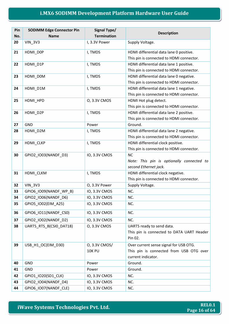
Pin
No.
SODIMM Edge Connector Pin
Name
Signal Type/
Termination Description
20 VIN_3V3 I, 3.3V Power Supply Voltage.
21 HDMI_D0P I, TMDS HDMI differential data lane 0 positive.
This pin is connected to HDMI connector.
22 HDMI_D1P I, TMDS HDMI differential data lane 1 positive.
This pin is connected to HDMI connector.
23 HDMI_D0M I, TMDS HDMI differential data lane 0 negative.
This pin is connected to HDMI connector.
24 HDMI_D1M I, TMDS HDMI differential data lane 1 negative.
This pin is connected to HDMI connector.
25 HDMI_HPD O, 3.3V CMOS HDMI Hot plug detect.
This pin is connected to HDMI connector.
26 HDMI_D2P I, TMDS HDMI differential data lane 2 positive.
This pin is connected to HDMI connector.
27 GND Power Ground.
28 HDMI_D2M I, TMDS HDMI differential data lane 2 negative.
This pin is connected to HDMI connector.
29 HDMI_CLKP I, TMDS HDMI differential clock positive.
This pin is connected to HDMI connector.
30 GPIO2_IO03(NANDF_D3) IO, 3.3V CMOS NC
Note: This pin is optionally connected to
second Ethernet jack.
31 HDMI_CLKM I, TMDS HDMI differential clock negative.
This pin is connected to HDMI connector.
32 VIN_3V3 O, 3.3V Power Supply Voltage.
33 GPIO6_IO09(NANDF_WP_B) IO, 3.3V CMOS NC.
34 GPIO2_IO06(NANDF_D6) IO, 3.3V CMOS NC.
35 GPIO5_IO02(EIM_A25) IO, 3.3V CMOS NC.
36 GPIO6_IO11(NANDF_CS0) IO, 3.3V CMOS NC.
37 GPIO2_IO02(NANDF_D2) IO, 3.3V CMOS NC.
38 UART5_RTS_B(CSI0_DAT18) O, 3.3V CMOS UART5 ready to send data.
This pin is connected to DATA UART Header
Pin 02.
39 USB_H1_OC(EIM_D30) O, 3.3V CMOS/
10K PU
Over current sense signal for USB OTG.
This pin is connected from USB OTG over
current indicator.
40 GND Power Ground.
41 GND Power Ground.
42 GPIO1_IO20(SD1_CLK) IO, 3.3V CMOS NC.
43 GPIO2_IO04(NANDF_D4) IO, 3.3V CMOS NC.
44 GPIO6_IO07(NANDF_CLE) IO, 3.3V CMOS NC.
REL0.1 Page 17 of 64
iWave Systems Technologies Pvt. Ltd.
i.MX6 SODIMM Development Platform Hardware User Guide
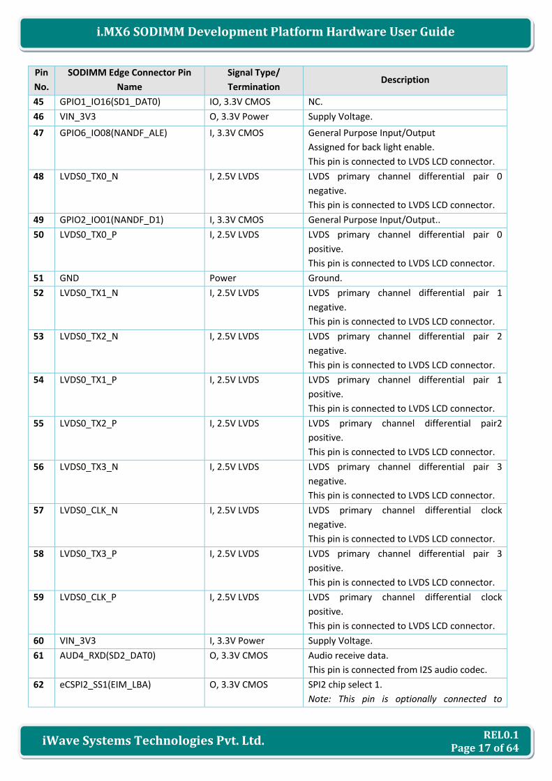
Pin
No.
SODIMM Edge Connector Pin
Name
Signal Type/
Termination Description
45 GPIO1_IO16(SD1_DAT0) IO, 3.3V CMOS NC.
46 VIN_3V3 O, 3.3V Power Supply Voltage.
47 GPIO6_IO08(NANDF_ALE) I, 3.3V CMOS General Purpose Input/Output
Assigned for back light enable.
This pin is connected to LVDS LCD connector.
48 LVDS0_TX0_N I, 2.5V LVDS
LVDS primary channel differential pair 0
negative.
This pin is connected to LVDS LCD connector.
49 GPIO2_IO01(NANDF_D1) I, 3.3V CMOS General Purpose Input/Output..
50 LVDS0_TX0_P I, 2.5V LVDS
LVDS primary channel differential pair 0
positive.
This pin is connected to LVDS LCD connector.
51 GND Power Ground.
52 LVDS0_TX1_N I, 2.5V LVDS LVDS primary channel differential pair 1
negative.
This pin is connected to LVDS LCD connector.
53 LVDS0_TX2_N I, 2.5V LVDS LVDS primary channel differential pair 2
negative.
This pin is connected to LVDS LCD connector.
54 LVDS0_TX1_P I, 2.5V LVDS LVDS primary channel differential pair 1
positive.
This pin is connected to LVDS LCD connector.
55 LVDS0_TX2_P I, 2.5V LVDS LVDS primary channel differential pair2
positive.
This pin is connected to LVDS LCD connector.
56 LVDS0_TX3_N I, 2.5V LVDS LVDS primary channel differential pair 3
negative.
This pin is connected to LVDS LCD connector.
57 LVDS0_CLK_N I, 2.5V LVDS LVDS primary channel differential clock
negative.
This pin is connected to LVDS LCD connector.
58 LVDS0_TX3_P I, 2.5V LVDS LVDS primary channel differential pair 3
positive.
This pin is connected to LVDS LCD connector.
59 LVDS0_CLK_P I, 2.5V LVDS LVDS primary channel differential clock
positive.
This pin is connected to LVDS LCD connector.
60 VIN_3V3 I, 3.3V Power Supply Voltage.
61 AUD4_RXD(SD2_DAT0) O, 3.3V CMOS Audio receive data.
This pin is connected from I2S audio codec.
62 eCSPI2_SS1(EIM_LBA) O, 3.3V CMOS SPI2 chip select 1.
Note: This pin is optionally connected to
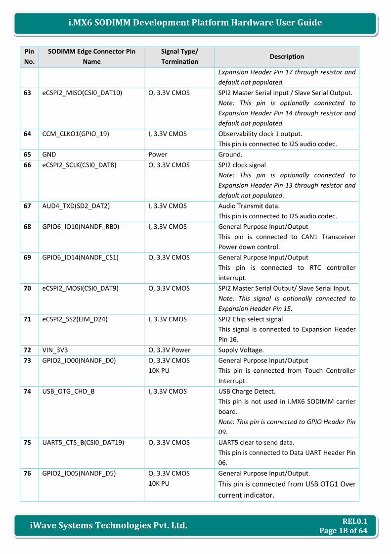
REL0.1 Page 18 of 64
iWave Systems Technologies Pvt. Ltd.
i.MX6 SODIMM Development Platform Hardware User Guide
Pin
No.
SODIMM Edge Connector Pin
Name
Signal Type/
Termination Description
Expansion Header Pin 17 through resistor and
default not populated.
63 eCSPI2_MISO(CSI0_DAT10) O, 3.3V CMOS SPI2 Master Serial Input / Slave Serial Output.
Note: This pin is optionally connected to
Expansion Header Pin 14 through resistor and
default not populated.
64 CCM_CLKO1(GPIO_19) I, 3.3V CMOS Observability clock 1 output.
This pin is connected to I2S audio codec.
65 GND Power Ground.
66 eCSPI2_SCLK(CSI0_DAT8) O, 3.3V CMOS SPI2 clock signal
Note: This pin is optionally connected to
Expansion Header Pin 13 through resistor and
default not populated.
67 AUD4_TXD(SD2_DAT2) I, 3.3V CMOS Audio Transmit data.
This pin is connected to I2S audio codec.
68 GPIO6_IO10(NANDF_RB0) I, 3.3V CMOS General Purpose Input/Output
This pin is connected to CAN1 Transceiver
Power down control.
69 GPIO6_IO14(NANDF_CS1) O, 3.3V CMOS General Purpose Input/Output
This pin is connected to RTC controller
interrupt.
70 eCSPI2_MOSI(CSI0_DAT9) O, 3.3V CMOS SPI2 Master Serial Output/ Slave Serial Input.
Note: This signal is optionally connected to
Expansion Header Pin 15.
71 eCSPI2_SS2(EIM_D24) I, 3.3V CMOS SPI2 Chip select signal
This signal is connected to Expansion Header
Pin 16.
72 VIN_3V3 O, 3.3V Power Supply Voltage.
73 GPIO2_IO00(NANDF_D0) O, 3.3V CMOS
10K PU
General Purpose Input/Output
This pin is connected from Touch Controller
Interrupt.
74 USB_OTG_CHD_B I, 3.3V CMOS USB Charge Detect.
This pin is not used in i.MX6 SODIMM carrier
board.
Note: This pin is connected to GPIO Header Pin
09.
75 UART5_CTS_B(CSI0_DAT19) O, 3.3V CMOS UART5 clear to send data.
This pin is connected to Data UART Header Pin
06.
76 GPIO2_IO05(NANDF_D5) O, 3.3V CMOS
10K PU
General Purpose Input/Output.
This pin is connected from USB OTG1 Over
current indicator.
REL0.1 Page 19 of 64
iWave Systems Technologies Pvt. Ltd.
i.MX6 SODIMM Development Platform Hardware User Guide
Pin
No.
SODIMM Edge Connector Pin
Name
Signal Type/
Termination Description
77 USBOTG_ID(GPIO_1) O, 3.3V CMOS
10K PU
USB OTG ID to identify Host & Device.
This pin is connected from Micro USB OTG
connector.
78 GPIO2_IO07(NANDF_D7) I, 3.3V CMOS General Purpose Input/Output.
Note: This pin is optionally connected to USB
OTG Power enable through resistor and
Default not populated.
79 GND Power Ground.
80 GPIO4_IO20(DI0_PIN4) IO, 3.3V CMOS General Purpose Input/Output.
This pin is connected to GPIO Header Pin 12
81 USB_OTG_DP IO, DIFF USB OTG data positive.
This pin is connected to Micro USB OTG
connector.
82 SATA_TXP I, DIFF SATA0 transmit output differential positive.
This pin is connected to SATA connector.
83 USB_OTG_DN IO, DIFF USB OTG data negative.
This pin is connected to Micro USB OTG
connector.
84 SATA_TXM I, DIFF SATA0 transmit output differential negative.
This pin is connected to SATA connector.
85 SATA_RXP O, DIFF SATA0 receive input differential positive.
This pin is connected to SATA connector.
86 GPIO6_IO31(EIM_BCLK) I, 3.3V CMOS General Purpose Input/Output
Assigned as SATA Power Control.
Note: This pin is optionally connected to SATA
Connector which is default not populated.
87 SATA_RXM O, DIFF/ SATA0 receive input differential negative.
This pin is connected to SATA connector.
88 VIN_3V3 O, 3.3V Power Supply Voltage.
89 AUD4_TXFS(SD2_DAT1) I, 3.3V CMOS Audio transmit frame synchronization.
This pin is connected to I2S audio codec.
90 AUD4_TXC(SD2_DAT3) I, 3.3V CMOS Audio transmit clock
This pin is connected to I2S audio codec.
91 AUD4_RXC(SD2_CMD) O, 3.3V CMOS Audio receive clock
This pin is connected to GPIO Header Pin 10.
92 AUD4_RXFS(SD2_CLK) O, 3.3V CMOS Audio receive frame synchronization.
This pin is connected to GPIO Header Pin 11.
93 GPIO6_IO01(CSI0_DAT15) O, 3.3V CMOS NC.
Note: This pin is connected from camera
connector.
REL0.1 Page 20 of 64
iWave Systems Technologies Pvt. Ltd.
i.MX6 SODIMM Development Platform Hardware User Guide
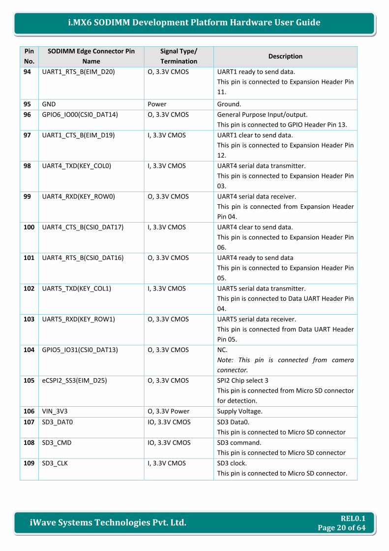
Pin
No.
SODIMM Edge Connector Pin
Name
Signal Type/
Termination Description
94 UART1_RTS_B(EIM_D20) O, 3.3V CMOS
UART1 ready to send data.
This pin is connected to Expansion Header Pin
11.
95 GND Power Ground.
96 GPIO6_IO00(CSI0_DAT14) O, 3.3V CMOS General Purpose Input/output.
This pin is connected to GPIO Header Pin 13.
97 UART1_CTS_B(EIM_D19) I, 3.3V CMOS UART1 clear to send data.
This pin is connected to Expansion Header Pin
12.
98 UART4_TXD(KEY_COL0) I, 3.3V CMOS UART4 serial data transmitter.
This pin is connected to Expansion Header Pin
03.
99 UART4_RXD(KEY_ROW0) O, 3.3V CMOS UART4 serial data receiver.
This pin is connected from Expansion Header
Pin 04.
100 UART4_CTS_B(CSI0_DAT17) I, 3.3V CMOS UART4 clear to send data.
This pin is connected to Expansion Header Pin
06.
101 UART4_RTS_B(CSI0_DAT16) O, 3.3V CMOS UART4 ready to send data
This pin is connected to Expansion Header Pin
05.
102 UART5_TXD(KEY_COL1) I, 3.3V CMOS UART5 serial data transmitter.
This pin is connected to Data UART Header Pin
04.
103 UART5_RXD(KEY_ROW1) O, 3.3V CMOS UART5 serial data receiver.
This pin is connected from Data UART Header
Pin 05.
104 GPIO5_IO31(CSI0_DAT13) O, 3.3V CMOS NC.
Note: This pin is connected from camera
connector.
105 eCSPI2_SS3(EIM_D25) O, 3.3V CMOS SPI2 Chip select 3
This pin is connected from Micro SD connector
for detection.
106 VIN_3V3 O, 3.3V Power Supply Voltage.
107 SD3_DAT0 IO, 3.3V CMOS SD3 Data0.
This pin is connected to Micro SD connector
108 SD3_CMD IO, 3.3V CMOS SD3 command.
This pin is connected to Micro SD connector
109 SD3_CLK I, 3.3V CMOS SD3 clock.
This pin is connected to Micro SD connector.
REL0.1 Page 21 of 64
iWave Systems Technologies Pvt. Ltd.
i.MX6 SODIMM Development Platform Hardware User Guide
Pin
No.
SODIMM Edge Connector Pin
Name
Signal Type/
Termination Description
110 eCSPI2_SS0(CSI0_DAT11) O, 3.3V CMOS NC.
Note: This pin is connected from camera
connector.
111 SD3_DAT1 IO, 3.3V CMOS SD3 Data1.
This pin is connected to Micro SD connector.
112 SD3_DAT2 IO, 3.3V CMOS SD3 Data2.
This pin is connected to Micro SD connector.
113 GND Power Ground.
114 SD3_DAT3 IO, 3.3V CMOS SD3 Data3.
This pin is connected to Micro SD connector.
115 I2C3_SDA(GPIO_6) IO, 3.3V OD/ I2C3 data.
This pin is connected to I2C devices.
116 I2C3_SCL(GPIO_3) I, 3.3V OD/ I2C3 clock.
This pin is connected to I2C devices.
117 UART2_RXD(EIM_D27) O, 3.3V CMOS UART2 serial data receiver.
This pin is connected from Serial to USB
converter for Debug console.
118 UART2_TXD(EIM_D26) I, 3.3V CMOS UART2 serial data transmitter.
This pin is connected from Serial to USB
converter for Debug console.
119 GPIO5_IO18(CSI0_PIXCLK) O, 3.3V CMOS NC.
Note: This pin is connected from camera
connector.
120 GPIO5_IO30(CSI0_DAT12) O, 3.3V CMOS NC.
Note: This pin is connected from camera
connector.
121 GPIO5_IO21(CSI0_VSYNC) IO, 3.3V CMOS NC.
Note: This pin is connected from camera
connector.
122 GPIO7_IO13(GPIO_18) O, 3.3V CMOS NC.
Note: This pin is connected from camera
connector. 123 GPIO5_IO19(CSI0_MCLK) O, 3.3V CMOS NC.
Note: This pin is connected from camera
connector
124 VIN_3V3 O, 3.3V Power Supply Voltage.
125 PWM2_OUT(SD1_DAT2) I, 3.3V CMOS Pulse Width Modulation 2 Output.
This pin is connected to Expansion Header Pin
18.
126 GPIO5_IO20(CSI0_DATA_EN) O, 3.3V CMOS NC
Note: This pin is connected from camera
connector.
REL0.1 Page 22 of 64
iWave Systems Technologies Pvt. Ltd.
i.MX6 SODIMM Development Platform Hardware User Guide
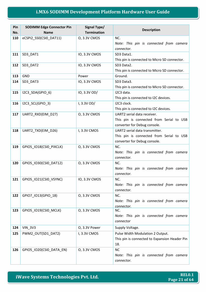
Pin
No.
SODIMM Edge Connector Pin
Name
Signal Type/
Termination Description
127 PCIE_TXP I, DIFF/ PCIe differential transmit line positive.
This pin is connected to PCIe connector.
128 PCIE_RXP O, DIFF PCIe differential receive line positive
This pin is connected to PCIe connector.
129 PCIE_TXM I, DIFF PCIe differential transmit line negative.
This pin is connected to PCIe connector.
130 PCIE_RXM O, DIFF PCIe differential receive line negative.
This pin is connected to PCIe connector.
131 GND Power Ground.
132 GPIO7_IO11(GPIO_16) I, 3.3V CMOS General Purpose Input/Output
This pin is configured to reset for all the
carrier board peripherals
133 GPIO7_IO12(GPIO_17) I, 3.3V CMOS General Purpose Input/Output
This pin is connected to PCIe connector
disable purpose.
134 GPIO1_IO02(GPIO_2) O, 3.3V CMOS General Purpose Input/Output
This pin is connected from PCIe connector for
wakeup purpose.
135 PCIE_REFCLK_DP(CLK1_P) I, DIFF PCIe differential reference clock positive
This pin is connected to PCIe connector.
136 GPIO4_IO13(KEY_ROW3) I, 3.3V CMOS General Purpose Input/Output
This pin is connected to LCD connector for LCD
power enable control.
137 PCIE_REFCLK_DM(CLK1_N) I, DIFF PCIe differential reference clock negative
This pin is connected to PCIe connector.
138 PWM1_OUT(GPIO_9) I, 3.3V CMOS Pulse Width Modulation 1 Output.
This pin is connected to 10.4” LVDS LCD
backlight driver IC and 12V LCD backlight
connector.
Note: This pin is optionally connected to 10.4”
LVDS connector.
139 GPIO4_IO12(KEY_COL3) IO, 3.3V CMOS General Purpose Input/Output
This pin is connected to GPIO Header Pin 14.
140 USB_H1_PWR(GPIO_0) I, 3.3V CMOS Power enable signal to control USB OTG2
VBUS voltage.
141 PWM4_OUT(SD1_CMD) I, 3.3V CMOS Pulse Width Modulation 4 Output.
This pin is optionally connected to USB host
power pin which is default not populated.
142 VIN_3V3 O, 3.3V Power Supply Voltage.
143 DI0_PIN3 I, 3.3V CMOS Parallel LCD VSYNC.
This pin is connected to LCD connector.

REL0.1 Page 23 of 64
iWave Systems Technologies Pvt. Ltd.
i.MX6 SODIMM Development Platform Hardware User Guide
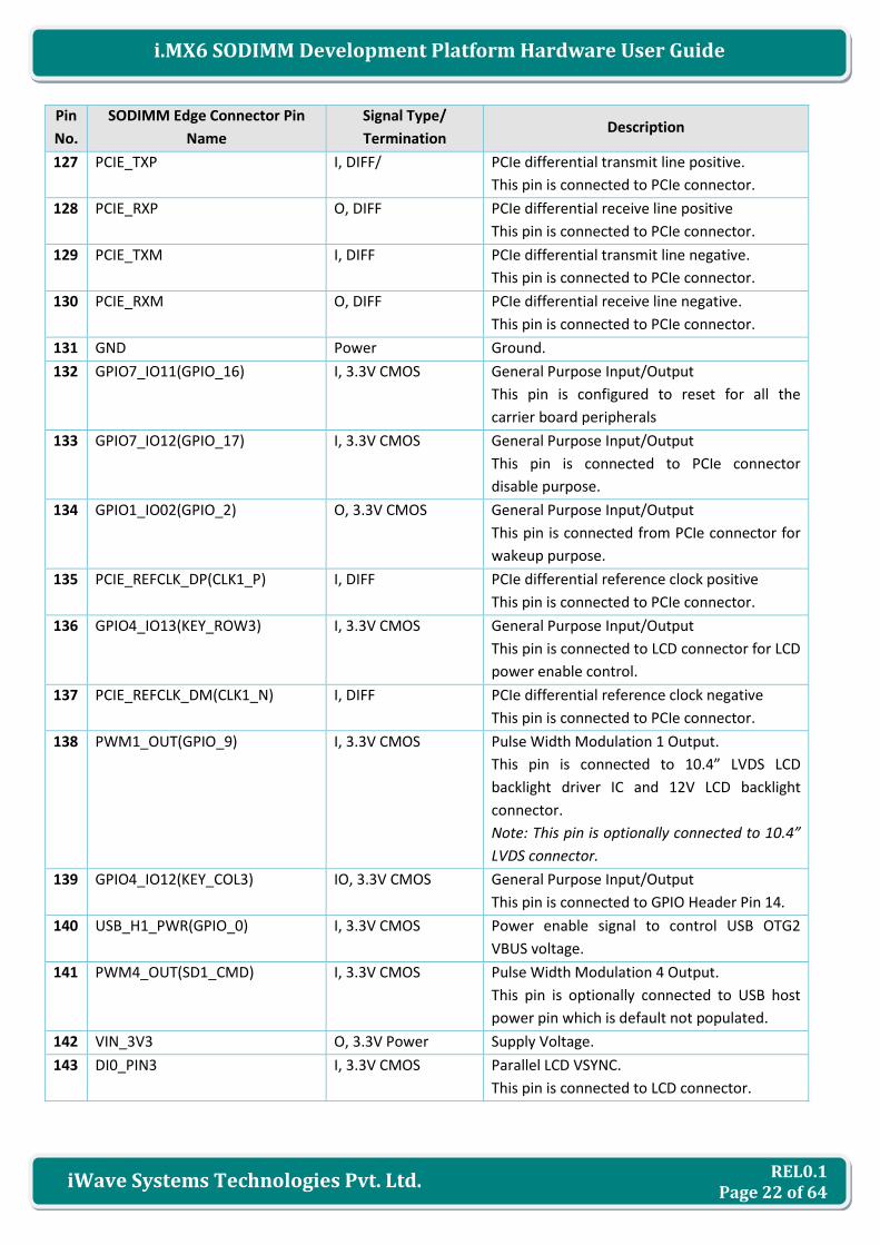
Pin
No.
SODIMM Edge Connector Pin
Name
Signal Type/
Termination Description
144 DI0_PIN2 I, 3.3V CMOS Parallel LCD HSYNC
This pin is connected to LCD connector.
145 DI0_DISP_CLK I, 3.3V CMOS Parallel LCD Clock.
This pin is connected to LCD connector.
146 DI0_PIN15 I, 3.3V CMOS Parallel LCD Enable.
This pin is connected to LCD connector.
147 PWM3_OUT(SD1_DAT1) I, 3.3V CMOS Pulse Width Modulation 3 Output.
This pin is connected to LCD connector for
brightness control.
148 DISP0_DAT16 I, 3.3V CMOS Parallel LCD data 16 (Red data0).
This pin is connected to LCD connector
149 DISP0_DAT17 I, 3.3V CMOS Parallel LCD data 17 (Red data1).
This pin is connected to LCD connector
150 DISP0_DAT18 I, 3.3V CMOS Parallel LCD data 18 (Red data2).
This pin is connected to LCD connector
151 GND Power Ground.
152 DISP0_DAT19 I, 3.3V CMOS Parallel LCD data 19 (Red data3).
This pin is connected to LCD connector.
153 DISP0_DAT20 I, 3.3V CMOS Parallel LCD data 20 (Red data4).
This pin is connected to LCD connector
154 DISP0_DAT21 I, 3.3V CMOS Parallel LCD data 21 (Red data5).
This pin is connected to LCD connector
155 DISP0_DAT22 I, 3.3V CMOS Parallel LCD data 22 (Red data6).
This pin is connected to LCD connector
156 DISP0_DAT23 I, 3.3V CMOS Parallel LCD data 23 (Red data7).
This pin is connected to LCD connector
157 DISP0_DAT8 I, 3.3V CMOS Parallel LCD data 8 (Green data0).
This pin is connected to LCD connector
158 DISP0_DAT9 I, 3.3V CMOS Parallel LCD data 9 (Green data1).
This pin is connected to LCD connector
159 DISP0_DAT10 I, 3.3V CMOS Parallel LCD data 10 (Green data2).
This pin is connected to LCD connector
160 VIN_3V3 I, 3.3V Power Supply Voltage.
161 DISP0_DAT11 I, 3.3V CMOS Parallel LCD data 11 (Green data3).
This pin is connected to LCD connector
162 DISP0_DAT12 I, 3.3V CMOS Parallel LCD data 12 (Green data4).
This pin is connected to LCD connector
163 DISP0_DAT13 I, 3.3V CMOS Parallel LCD data 13 (Green data5).
This pin is connected to LCD connector
164 DISP0_DAT14 I, 3.3V CMOS Parallel LCD data 14 (Green data6).
This pin is connected to LCD connector
REL0.1 Page 24 of 64
iWave Systems Technologies Pvt. Ltd.
i.MX6 SODIMM Development Platform Hardware User Guide
Pin
No.
SODIMM Edge Connector Pin
Name
Signal Type/
Termination Description
165 DISP0_DAT15 I, 3.3V CMOS Parallel LCD data 15 (Green data7).
This pin is connected to LCD connector
166 DISP0_DAT0 I, 3.3V CMOS Parallel LCD data 0 (Blue data0).
This pin is connected to LCD connector
through resistor and default not populated.
167 DISP0_DAT1 I, 3.3V CMOS Parallel LCD data 1 (Blue data1).
This pin is connected to LCD connector
through resistor and default not populated.
168 DISP0_DAT2 I, 3.3V CMOS Parallel LCD data 2 (Blue data2).
This pin is connected to LCD connector
169 GND Power Ground.
170 DISP0_DAT3 I, 3.3V CMOS Parallel LCD data 3 (Blue data3)
This pin is connected to LCD connector
171 DISP0_DAT4 I, 3.3V CMOS Parallel LCD data 4 (Blue data4).
This pin is connected to LCD connector
172 DISP0_DAT5 I, 3.3V CMOS Parallel LCD data 5 (Blue data5).
This pin is connected to LCD connector
173 DISP0_DAT6 I, 3.3V CMOS Parallel LCD data 6 (Blue data6).
This pin is connected to LCD connector
174 DISP0_DAT7 I, 3.3V CMOS Parallel LCD data 7 (Blue data7).
This pin is connected to LCD connector
175 CAN2_RX(KEY_ROW4) O, 3.3V CMOS Receive input for CAN2 bus.
This pin is connected from Expansion Header
Pin 08.
176 CAN1_RX(GPIO_8) O, 3.3V CMOS Receive input for CAN1 bus.
This pin is connected from CAN1 Transceiver.
177 CAN2_TX(KEY_COL4) I, 3.3V CMOS Transmit output for CAN2 bus.
This pin is connected to Expansion Header Pin
07.
178 CAN1_TX(GPIO_7) I, 3.3V CMOS Transmit output for CAN1 bus.
This pin is connected to CAN1 Transceiver.
179 GPIO4_IO10(KEY_COL2) O, 3V CMOS General Purpose Input/Output.
This pin is connected from Push button for
power On/Off control.
Note: This function is not used in i.MX6
SODIMM SOM
180 VIN_3V3 I, 3.3V Power Supply Voltage.
181 GPIO4_IO11(KEY_ROW2) IO, 3V CMOS General Purpose Input/Output.
This pin is connected to GPIO Header Pin 15.
182 BOOT_MODE0 O, 3.3V CMOS Boot Mode Select bit0.
This pin is connected from two-bit DIP switch
for selecting the desired boot mode.

REL0.1 Page 25 of 64
iWave Systems Technologies Pvt. Ltd.
i.MX6 SODIMM Development Platform Hardware User Guide
Pin
No.
SODIMM Edge Connector Pin
Name
Signal Type/
Termination Description
183 VRTC_3V0 O, 3V Power This pin is connected from RTC coin cell
holder.
184 BOOT_MODE1 O, 3.3V CMOS Boot Mode Select bit1.
This pin is connected from two-bit DIP switch
for selecting the desired boot mode.
185 GND Power Ground.
186 GND Power Ground.
187 n_RST_OUT O, 3V CMOS Active low reset button input.
This pin is connected from Push button for
reset control.
188 USB_H1_DP IO, 3.3V CMOS USB Host Port 1 data positive.
This pin is connected to two port USB Hub.
189 NC - This pin is connected to GPIO Header Pin 16.
190 USB_H1_DN IO, 3.3V CMOS USB Host Port 1 data negative.
This pin is connected to two port USB Hub
191 JTAG_TDO I, 3.3V CMOS JTAG Test Data Output.
This pin is connected to JTAG Header.
192 VIN_3V3 I, 3.3V Power Supply Voltage.
193 JTAG_TRSTB O, 3.3V CMOS JTAG Test Reset.
This pin is connected from JTAG Header
194 NC - This pin is connected to GPIO Header Pin 17.
195 JTAG_TDI O, 3.3V CMOS JTAG Test Data Input
This pin is connected from JTAG Header.
196 NC - NC.
197 JTAG_TCK O, 3.3V CMOS/
10K PU
JTAG Test Clock.
This pin is connected from JTAG Header.
198 GND Power Ground.
199 JTAG_TMS O, 3.3V CMOS/
10K UP
JTAG Test Mode Select.
This pin is connected from JTAG Header.
200 VBUS_5V O, Power 5V Reference voltage to USB controller.
REL0.1 Page 26 of 64
iWave Systems Technologies Pvt. Ltd.
i.MX6 SODIMM Development Platform Hardware User Guide
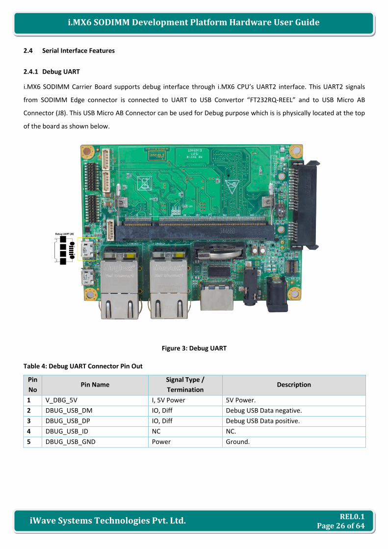
2.4 Serial Interface Features
2.4.1 Debug UART
i.MX6 SODIMM Carrier Board supports debug interface through i.MX6 CPU’s UART2 interface. This UART2 signals
from SODIMM Edge connector is connected to UART to USB Convertor “FT232RQ-REEL” and to USB Micro AB
Connector (J8). This USB Micro AB Connector can be used for Debug purpose which is is physically located at the top
of the board as shown below.
Figure 3: Debug UART
Table 4: Debug UART Connector Pin Out
Pin
No Pin Name
Signal Type /
Termination Description
1 V_DBG_5V I, 5V Power 5V Power.
2 DBUG_USB_DM IO, Diff Debug USB Data negative.
3 DBUG_USB_DP IO, Diff Debug USB Data positive.
4 DBUG_USB_ID NC NC.
5 DBUG_USB_GND Power Ground.
REL0.1 Page 27 of 64
iWave Systems Technologies Pvt. Ltd.
i.MX6 SODIMM Development Platform Hardware User Guide
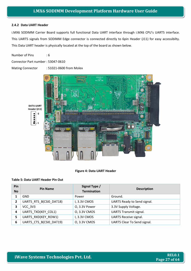
2.4.2 Data UART Header
i.MX6 SODIMM Carrier Board supports full functional Data UART interface through i.MX6 CPU’s UART5 interface.
This UART5 signals from SODIMM Edge connector is connected directly to 6pin Header (J11) for easy accessibilty.
This Data UART header is physically located at the top of the board as shown below.
Number of Pins : 6
Connector Part number : 53047-0610
Mating Connector : 51021-0600 from Molex
Figure 4: Data UART Header
Table 5: Data UART Header Pin Out
Pin
No Pin Name
Signal Type /
Termination Description
1 GND Power Ground.
2 UART5_RTS_B(CSI0_DAT18) I, 3.3V CMOS UART5 Ready to Send signal.
3 VCC_3V3 O, 3.3V Power 3.3V Supply Voltage.
4 UART5_TXD(KEY_COL1) O, 3.3V CMOS UART5 Transmit signal.
5 UART5_RXD(KEY_ROW1) I, 3.3V CMOS UART5 Receive signal.
6 UART5_CTS_B(CSI0_DAT19) O, 3.3V CMOS UART5 Clear To Send signal.
REL0.1 Page 28 of 64
iWave Systems Technologies Pvt. Ltd.
i.MX6 SODIMM Development Platform Hardware User Guide
2.5 Communication Features
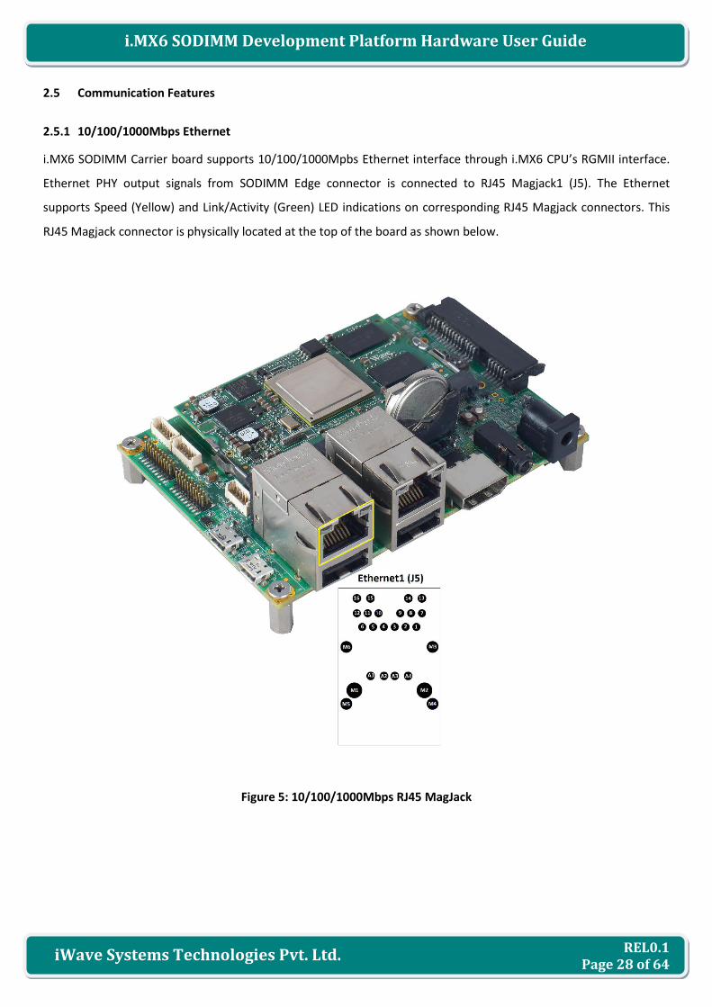
2.5.1 10/100/1000Mbps Ethernet
i.MX6 SODIMM Carrier board supports 10/100/1000Mpbs Ethernet interface through i.MX6 CPU’s RGMII interface.
Ethernet PHY output signals from SODIMM Edge connector is connected to RJ45 Magjack1 (J5). The Ethernet
supports Speed (Yellow) and Link/Activity (Green) LED indications on corresponding RJ45 Magjack connectors. This
RJ45 Magjack connector is physically located at the top of the board as shown below.
Figure 5: 10/100/1000Mbps RJ45 MagJack
REL0.1 Page 29 of 64
iWave Systems Technologies Pvt. Ltd.
i.MX6 SODIMM Development Platform Hardware User Guide
Table 6: RJ45 MagJack1 Pin Out
Pin
No Pin Name
Signal Type /
Termination Description
1 TRCT1_3 - Transformer Centre Tap 3
2 GPHY_CTXRXM IO, Diff Ethernet differential pair 2 negative.
3 GPHY_CTXRXP IO, Diff Ethernet differential pair 2 positive.
4 GPHY_BTXRXP IO, Diff Ethernet differential pair 1 positive.
5 GPHY_BTXRXM IO, Diff Ethernet differential pair 1 negative.
6 TRCT1_2 - Transformer Centre Tap 2.
7 TRCT1_4 - Transformer Centre Tap 4.
8 GPHY_DTXRXP - Ethernet differential pair 3 positive.
9 GPHY_DTXRXM - Ethernet differential pair 3 negative.
10 GPHY_ATXRXM - Ethernet differential pair 0 negative.
11 GPHY_ATXRXP - Ethernet differential pair 0 positive.
12 TRCT1_1 - Transformer Centre Tap1.
13 ETH1_LED-Y_K I, 3.3V CMOS Ethernet Speed indication Yellow LED Cathode.
14 ETH1_LED-Y_A I, 3.3V Power Ethernet Speed indication Yellow LED Anode.
15 ETH1_LED-GO_K I, 3.3V CMOS Ethernet Link/Activity indication Green LED Cathode.
16 ETH1_LED-GO_A I, 3.3V Power Ethernet Link/Activity indication Green LED Anode.

REL0.1 Page 30 of 64
iWave Systems Technologies Pvt. Ltd.
i.MX6 SODIMM Development Platform Hardware User Guide
2.5.2 USB2.0 Device
i.MX6 SODIMM Carrier Board supports High Speed USB2.0 device interface through i.MX6 CPU’s USBOTG interface.
This USBOTG signals from SODIMM Edge connector is directly connected to USB Micro AB connector (J6). USB OTG
as device functionality only supported in i.MX6 SODIMM Carrier Board. This USB Micro AB connector is physically
located at the top of the board as shown below.
Figure 6: USB2.0 Device Port
Table 7: USB2.0 Device Connector Pin Out
Pin
No Pin Name
Signal Type /
Termination Description
1 V_OTG2 I, 5V Power 5V Supply Voltage.
2 USB_OTG_DN IO, Diff USB OTG Data negative.
3 USB_OTG_DP IO, Diff USB OTG Data Positive.
4 USBOTG_ID(GPIO_1) O, 3.3V CMOS/
10K PU
USD OTG ID signal.
5 GND Power Ground.
REL0.1 Page 31 of 64
iWave Systems Technologies Pvt. Ltd.
i.MX6 SODIMM Development Platform Hardware User Guide
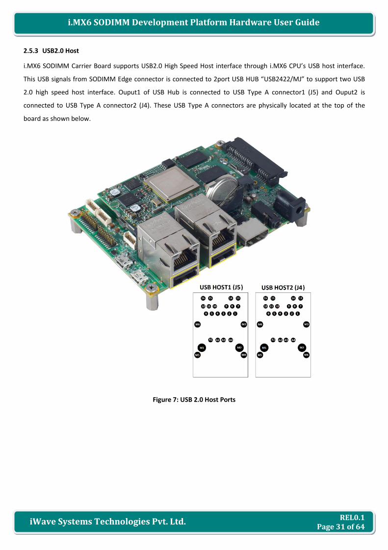
2.5.3 USB2.0 Host
i.MX6 SODIMM Carrier Board supports USB2.0 High Speed Host interface through i.MX6 CPU’s USB host interface.
This USB signals from SODIMM Edge connector is connected to 2port USB HUB “USB2422/MJ” to support two USB
2.0 high speed host interface. Ouput1 of USB Hub is connected to USB Type A connector1 (J5) and Ouput2 is
connected to USB Type A connector2 (J4). These USB Type A connectors are physically located at the top of the
board as shown below.
Figure 7: USB 2.0 Host Ports
REL0.1 Page 32 of 64
iWave Systems Technologies Pvt. Ltd.
i.MX6 SODIMM Development Platform Hardware User Guide
Table 8: USB 2.0 Host 1 Connector (J5) Pin Out
Pin
No Pin Name
Signal Type /
Termination Description
A1 V_HOST O, 5V Power 5V Supply Voltage.
A2 USB_HOST1- IO, Diff USB Host Port 1 Data Negative.
A3 USB_HOST1+ IO, Diff USB Host Port 1 Data Positive.
A4 GND Power Ground.
Table 9: USB 2.0 Host 2 Connector (J4) Pin Out
Pin
No Pin Name
Signal Type /
Termination Description
A1 V_OTG1 O, 5V Power 5V Supply Voltage.
A2 USB_HOST2- IO, Diff USB Host Port 2 Data Negative.
A3 USB_HOST2+ IO, Diff USB Host Port 2 Data Positive.
A4 GND Power Ground.
REL0.1 Page 33 of 64
iWave Systems Technologies Pvt. Ltd.
i.MX6 SODIMM Development Platform Hardware User Guide
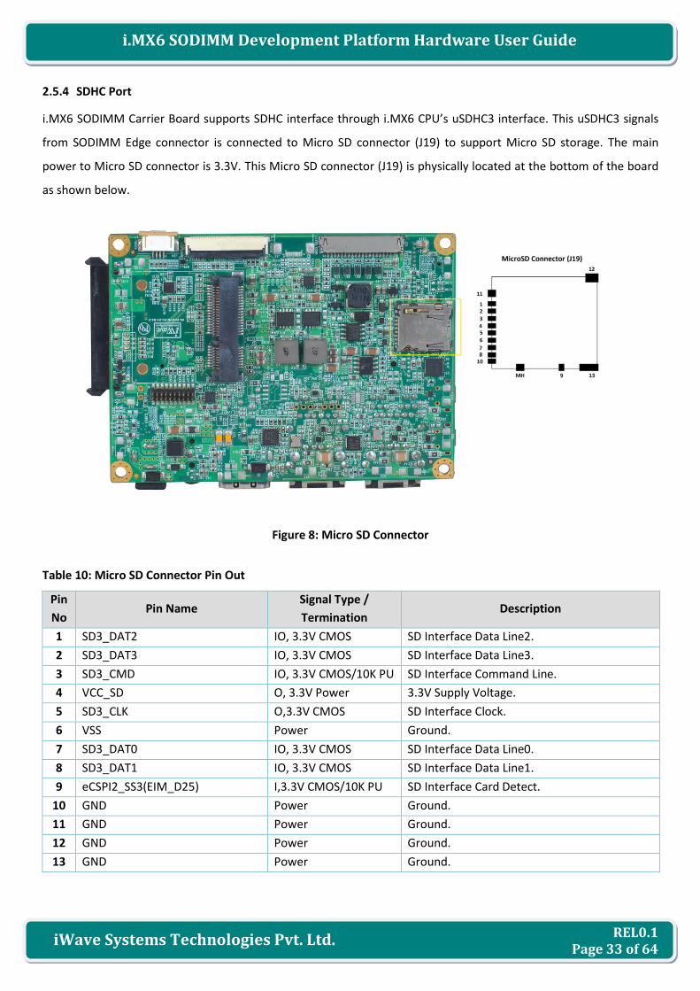
2.5.4 SDHC Port
i.MX6 SODIMM Carrier Board supports SDHC interface through i.MX6 CPU’s uSDHC3 interface. This uSDHC3 signals
from SODIMM Edge connector is connected to Micro SD connector (J19) to support Micro SD storage. The main
power to Micro SD connector is 3.3V. This Micro SD connector (J19) is physically located at the bottom of the board
as shown below.
Figure 8: Micro SD Connector
Table 10: Micro SD Connector Pin Out
Pin
No Pin Name
Signal Type /
Termination Description
1 SD3_DAT2 IO, 3.3V CMOS SD Interface Data Line2.
2 SD3_DAT3 IO, 3.3V CMOS SD Interface Data Line3.
3 SD3_CMD IO, 3.3V CMOS/10K PU SD Interface Command Line.
4 VCC_SD O, 3.3V Power 3.3V Supply Voltage.
5 SD3_CLK O,3.3V CMOS SD Interface Clock.
6 VSS Power Ground.
7 SD3_DAT0 IO, 3.3V CMOS SD Interface Data Line0.
8 SD3_DAT1 IO, 3.3V CMOS SD Interface Data Line1.
9 eCSPI2_SS3(EIM_D25) I,3.3V CMOS/10K PU SD Interface Card Detect.
10 GND Power Ground.
11 GND Power Ground.
12 GND Power Ground.
13 GND Power Ground.

REL0.1 Page 34 of 64
iWave Systems Technologies Pvt. Ltd.
i.MX6 SODIMM Development Platform Hardware User Guide
2.5.5 CAN Port
i.MX6 SODIMM Carrier Board supports CAN interface through i.MX6 CPU’s CAN1 interface. This CAN1 signals from
SODIMM Edge connector is connected to CAN Bus transceiver “SN65HVD230DR” and to 6pin header (J15). This CAN
header is physically located at the top of the board as shown below.
Figure 9: CAN Header
Table 11: CAN Header Pin Out
Pin
No Pin Name
Signal Type /
Termination Description
1 VCC_5V_CAN O, 5V Power 5V Supply Voltage.
2 NC - NC.
3 CANL IO, Diff CAN Differential negative.
4 GND Power Ground.
5 CANH IO, Diff CAN Differential positive.
6 GND Power Ground.
REL0.1 Page 35 of 64
iWave Systems Technologies Pvt. Ltd.
i.MX6 SODIMM Development Platform Hardware User Guide
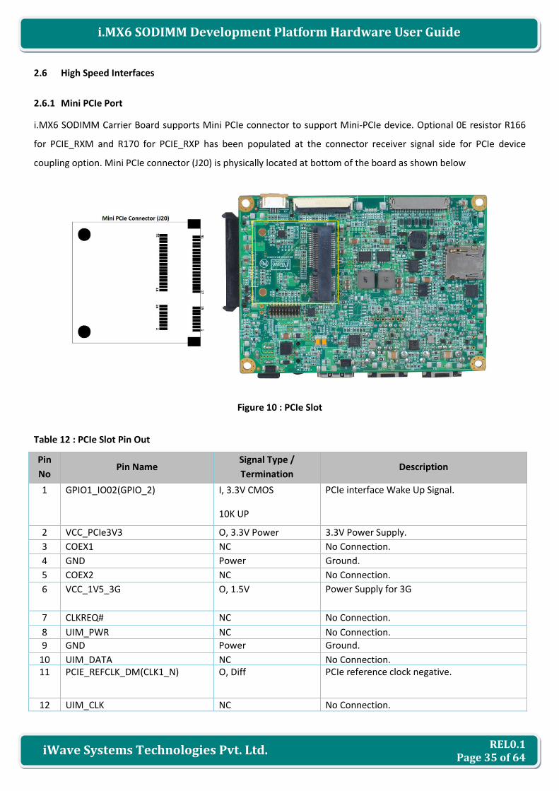
2.6 High Speed Interfaces
2.6.1 Mini PCIe Port
i.MX6 SODIMM Carrier Board supports Mini PCIe connector to support Mini-PCIe device. Optional 0E resistor R166
for PCIE_RXM and R170 for PCIE_RXP has been populated at the connector receiver signal side for PCIe device
coupling option. Mini PCIe connector (J20) is physically located at bottom of the board as shown below
Figure 10 : PCIe Slot
Table 12 : PCIe Slot Pin Out
Pin
No Pin Name
Signal Type /
Termination Description
1 GPIO1_IO02(GPIO_2) I, 3.3V CMOS
10K UP
PCIe interface Wake Up Signal.
2 VCC_PCIe3V3 O, 3.3V Power 3.3V Power Supply.
3 COEX1 NC No Connection.
4 GND Power Ground.
5 COEX2 NC No Connection.
6 VCC_1V5_3G O, 1.5V Power Supply for 3G
7 CLKREQ# NC No Connection.
8 UIM_PWR NC No Connection.
9 GND Power Ground.
10 UIM_DATA NC No Connection. 11 PCIE_REFCLK_DM(CLK1_N) O, Diff PCIe reference clock negative.
12 UIM_CLK NC No Connection.
REL0.1 Page 36 of 64
iWave Systems Technologies Pvt. Ltd.
i.MX6 SODIMM Development Platform Hardware User Guide
13 PCIE_REFCLK_DP(CLK1_P) O, Diff PCIe reference clock positive.
14 UIM_RESET NC No Connection.
15 GND Power Ground
16 UIM_VPP NC No Connection.
17 RSVD(UIM_C8) NC No Connection.
18 GND Power Ground.
19 RSVD(UIM_C84 NC No Connection.
20 GPIO7_IO12(GPIO_17) O, 3.3V CMOS Wireless Disable.
21 GND Power Ground.
22 GPIO7_IO11(GPIO_16) O, 3.3V CMOS Reset Input, Active Low. 23 PCIE_RXM I, Diff PCIe Receive Pair Negative
24 VCC_PCIe3V3 O, 3.3V Power 3.3V Power Supply.
25 PCIE_RXP I, Diff PCIe Receive Pair Positive 26 GND Power Ground
27 GND Power Ground
28 VCC_1V5_3G O, 1.5V Power Supply for 3G
29 GND Power Ground
30 I2C3_SCL(GPIO_3) O, 3.3V CMOS System Management Bus Clock.
31 PCIE_TXM O, Diff PCIe Transmit Pair negative
32 I2C3_SDA(GPIO_6) IO, 3.3V CMOS System Management Data.
33 PCIE_TXP O, Diff PCIe Transmit Pair Positive
34 GND Power Ground
35 GND Power Ground
36 3G_USB_D- IO, Diff USB Host Data negative. This signal is
optionally connected to USB hub and J4B USB
connector.
37 GND Power Ground
38 3G_USB_D+ IO, Diff USB Host Data negative. This signal is
optionally connected to USB hub and J4B USB
connector.
39 VCC_PCIe3V3 O, 3.3V Power 3.3V Power Supply.
40 GND Power Ground
41 VCC_PCIe3V3 O, 3.3V 3.3V Power Supply.
42 LED_WWAN# I, 3.3V CMOS
LED Enable.
Connected to red LED D15 and default
populated.
43 GND Power Ground
44 LED_WLAN# I, 3.3V CMOS
LED Enable.
Connected to red LED D16 and default
populated.
45 RSVD NC No Connection
REL0.1 Page 37 of 64
iWave Systems Technologies Pvt. Ltd.
i.MX6 SODIMM Development Platform Hardware User Guide
46 LED_WPAN# I, 3.3V CMOS
LED Enable.
Connected to red LED D17 and default
populated.
47 RSVD1 NC No Connection
48 VCC_1V5_3G O, 1.5V Power Supply for 3G
49 RSVD2 NC No Connection. 50 GND Power Ground
51 RSVD3 NC No Connection. 52 VCC_PCIe3V3 O, 3.3V Power 3.3V Power Supply.

REL0.1 Page 38 of 64
iWave Systems Technologies Pvt. Ltd.
i.MX6 SODIMM Development Platform Hardware User Guide
2.6.2 SATA Port
i.MX6 SODIMM Carrier Board supports one 22Pin SATA connector for SATA interface.SATA signals from SODIMM
connector are connected to standard 22pin SATA connector with power. This connector (J13) is physically located on
top of the board as shown below.
Figure 11 SATA Connector
Table 13 SATA Connector PinOut
Pin No Pin Name Signal Type /
Termination Description
S1 GND_S1 Power Ground.
S2 SATA_TXP O, Diff SATA Transmit pair positive. S3 SATA_TXM O, Diff SATA0 Transmit pair negative.
S4 GND_S4 Power Ground
S5 SATA_RXM I, Diff SATA Receive pair negative. S6 SATA_RXP I, Diff SATA Receive pair positive.
S7 GND_S7 Power Ground
P1 VCC_3.3V 3.3V 3.3V Power Supply.
P2 VCC_3.3V 3.3V 3.3V Power Supply.
P3 GPIO6_IO31(EIM_BCLK) O, 3.3V CMOS SATA power control pin. This pin is optionally
connected through resistor and default not
populated.
P4 GND Power Ground
P5 GND Power Ground
P6 GND Power Ground

REL0.1 Page 39 of 64
iWave Systems Technologies Pvt. Ltd.
i.MX6 SODIMM Development Platform Hardware User Guide
P7 5V_SATA O, 5V Power 5V Power Supply.
P8 5V_SATA O, 5V Power 5V Power Supply.
P9 5V_SATA O, 5V Power 5V Power Supply.
P10 GND Power Ground
P11 DAS_DSS Power This pin is optionally connected to ground
through resistor and default not populated.
P12 GND Power Ground
P13 VCC_12V O, 12V Power 12V Power Supply. This pin is optionally
connected through ferrate bead and default
not populated
P14 VCC_12V O, 12V Power 12V Power Supply. This pin is optionally
connected through ferrate bead and default
not populated
P15 VCC_12V O, 12V Power 12V Power Supply. This pin is optionally
connected through ferrate bead and default
not populated
SH1,SH2 M1, M2 Power Shield Ground through 1M resistor
REL0.1 Page 40 of 64
iWave Systems Technologies Pvt. Ltd.
i.MX6 SODIMM Development Platform Hardware User Guide
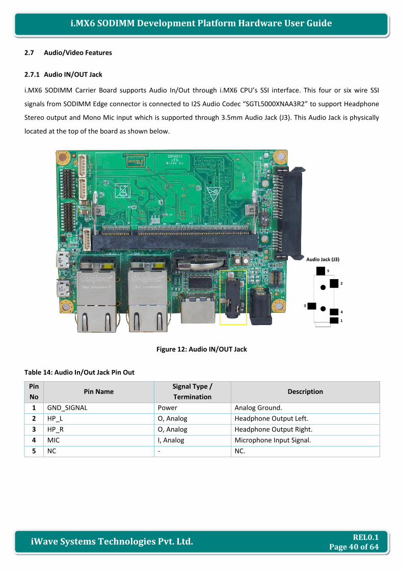
2.7 Audio/Video Features
2.7.1 Audio IN/OUT Jack
i.MX6 SODIMM Carrier Board supports Audio In/Out through i.MX6 CPU’s SSI interface. This four or six wire SSI
signals from SODIMM Edge connector is connected to I2S Audio Codec “SGTL5000XNAA3R2” to support Headphone
Stereo output and Mono Mic input which is supported through 3.5mm Audio Jack (J3). This Audio Jack is physically
located at the top of the board as shown below.
Figure 12: Audio IN/OUT Jack
Table 14: Audio In/Out Jack Pin Out
Pin
No Pin Name
Signal Type /
Termination Description
1 GND_SIGNAL Power Analog Ground.
2 HP_L O, Analog Headphone Output Left.
3 HP_R O, Analog Headphone Output Right.
4 MIC I, Analog Microphone Input Signal.
5 NC - NC.
REL0.1 Page 41 of 64
iWave Systems Technologies Pvt. Ltd.
i.MX6 SODIMM Development Platform Hardware User Guide
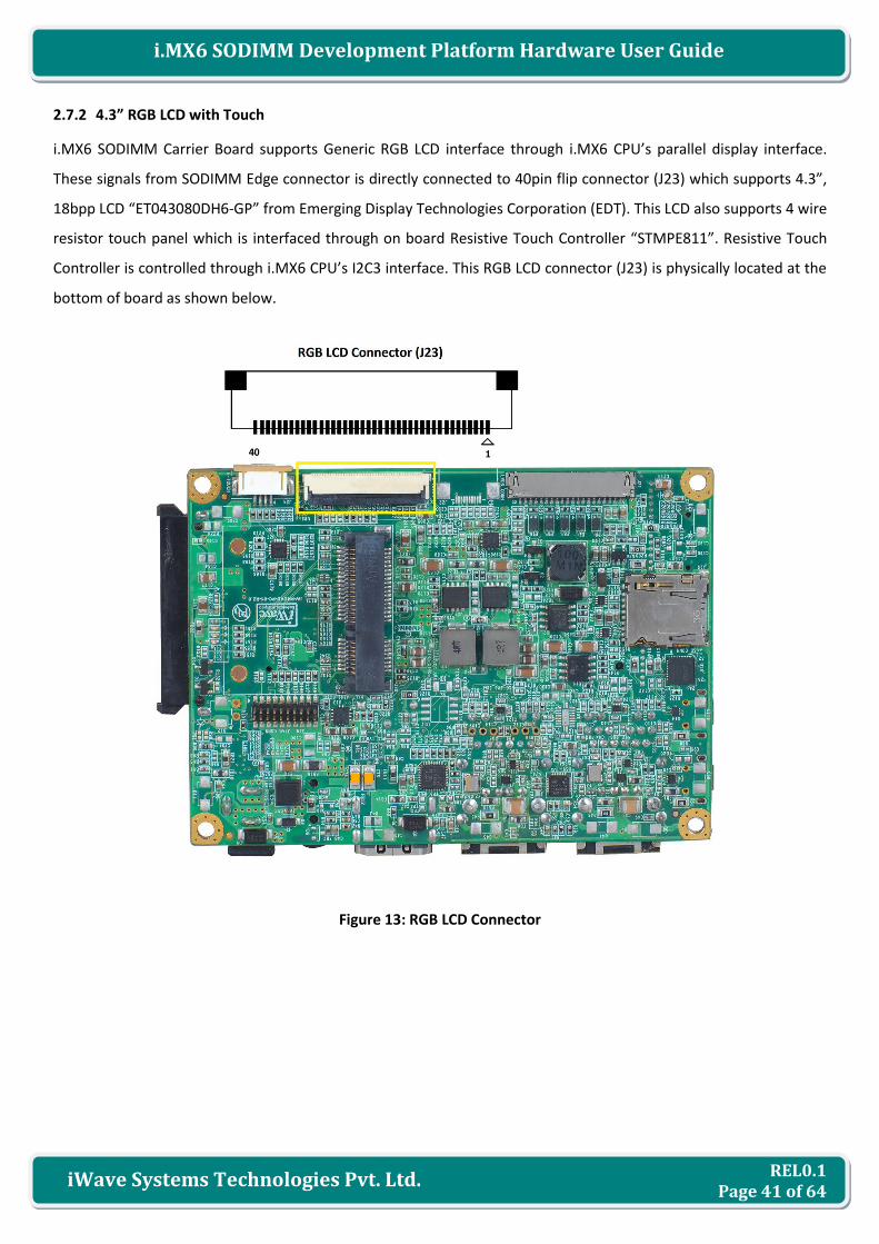
2.7.2 4.3” RGB LCD with Touch
i.MX6 SODIMM Carrier Board supports Generic RGB LCD interface through i.MX6 CPU’s parallel display interface.
These signals from SODIMM Edge connector is directly connected to 40pin flip connector (J23) which supports 4.3”,
18bpp LCD “ET043080DH6-GP” from Emerging Display Technologies Corporation (EDT). This LCD also supports 4 wire
resistor touch panel which is interfaced through on board Resistive Touch Controller “STMPE811”. Resistive Touch
Controller is controlled through i.MX6 CPU’s I2C3 interface. This RGB LCD connector (J23) is physically located at the
bottom of board as shown below.
Figure 13: RGB LCD Connector
REL0.1 Page 42 of 64
iWave Systems Technologies Pvt. Ltd.
i.MX6 SODIMM Development Platform Hardware User Guide
The same LCD connector can also support different size LCDs from Emerging Display Technologies Corporation as
listed below.
Compatible LCDs:
ET035080DH6 - 3.5" with Resistive Touch Panel
ET035080DM6 - 3.5" without Resistive Touch Panel
ET043080DH6 - 4.3" with Resistive Touch Panel
ET043080DM6 - 4.3" without Resistive Touch Panel
ET050080DH6 - 5.0" with Resistive Touch Panel
ET050080DM6 - 5.0" without Resistive Touch Panel
ET057080DH6 - 5.7" with Resistive Touch Panel
ET057080DM6 - 5.7" without Resistive Touch Panel
ET057090DHU - 5.7" with Resistive Touch Panel
ET057090DMU - 5.7" without Resistive Touch Panel
ET070080DH6 - 7.0" with Resistive Touch Panel
ET070080DM6 - 7.0" without Resistive Touch Panel
ETM070080ADH6- 7.0" with Capacitive Touch Panel
i.MX6 SODIMM Carrier Board can also optionally support capacitive touch panel through capacitive touch connector
(J22). This is the optional feature and by default not populated on board.
REL0.1 Page 43 of 64
iWave Systems Technologies Pvt. Ltd.
i.MX6 SODIMM Development Platform Hardware User Guide
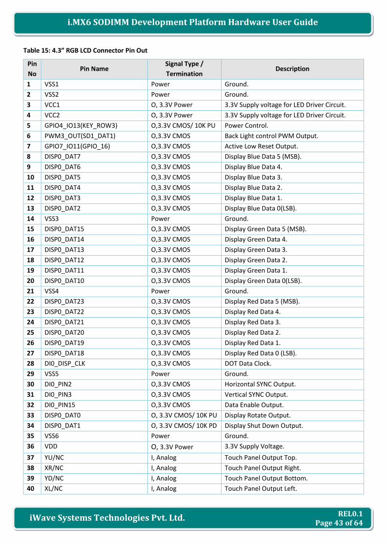
Table 15: 4.3” RGB LCD Connector Pin Out
Pin
No Pin Name
Signal Type /
Termination Description
1 VSS1 Power Ground.
2 VSS2 Power Ground.
3 VCC1 O, 3.3V Power 3.3V Supply voltage for LED Driver Circuit.
4 VCC2 O, 3.3V Power 3.3V Supply voltage for LED Driver Circuit.
5 GPIO4_IO13(KEY_ROW3) O,3.3V CMOS/ 10K PU Power Control.
6 PWM3_OUT(SD1_DAT1) O,3.3V CMOS Back Light control PWM Output.
7 GPIO7_IO11(GPIO_16) O,3.3V CMOS Active Low Reset Output.
8 DISP0_DAT7 O,3.3V CMOS Display Blue Data 5 (MSB).
9 DISP0_DAT6 O,3.3V CMOS Display Blue Data 4.
10 DISP0_DAT5 O,3.3V CMOS Display Blue Data 3.
11 DISP0_DAT4 O,3.3V CMOS Display Blue Data 2.
12 DISP0_DAT3 O,3.3V CMOS Display Blue Data 1.
13 DISP0_DAT2 O,3.3V CMOS Display Blue Data 0(LSB).
14 VSS3 Power Ground.
15 DISP0_DAT15 O,3.3V CMOS Display Green Data 5 (MSB).
16 DISP0_DAT14 O,3.3V CMOS Display Green Data 4.
17 DISP0_DAT13 O,3.3V CMOS Display Green Data 3.
18 DISP0_DAT12 O,3.3V CMOS Display Green Data 2.
19 DISP0_DAT11 O,3.3V CMOS Display Green Data 1.
20 DISP0_DAT10 O,3.3V CMOS Display Green Data 0(LSB).
21 VSS4 Power Ground.
22 DISP0_DAT23 O,3.3V CMOS Display Red Data 5 (MSB).
23 DISP0_DAT22 O,3.3V CMOS Display Red Data 4.
24 DISP0_DAT21 O,3.3V CMOS Display Red Data 3.
25 DISP0_DAT20 O,3.3V CMOS Display Red Data 2.
26 DISP0_DAT19 O,3.3V CMOS Display Red Data 1.
27 DISP0_DAT18 O,3.3V CMOS Display Red Data 0 (LSB).
28 DI0_DISP_CLK O,3.3V CMOS DOT Data Clock.
29 VSS5 Power Ground.
30 DI0_PIN2 O,3.3V CMOS Horizontal SYNC Output.
31 DI0_PIN3 O,3.3V CMOS Vertical SYNC Output.
32 DI0_PIN15 O,3.3V CMOS Data Enable Output.
33 DISP0_DAT0 O, 3.3V CMOS/ 10K PU Display Rotate Output.
34 DISP0_DAT1 O, 3.3V CMOS/ 10K PD Display Shut Down Output.
35 VSS6 Power Ground.
36 VDD O, 3.3V Power 3.3V Supply Voltage.
37 YU/NC I, Analog Touch Panel Output Top.
38 XR/NC I, Analog Touch Panel Output Right.
39 YD/NC I, Analog Touch Panel Output Bottom.
40 XL/NC I, Analog Touch Panel Output Left.
REL0.1 Page 44 of 64
iWave Systems Technologies Pvt. Ltd.
i.MX6 SODIMM Development Platform Hardware User Guide
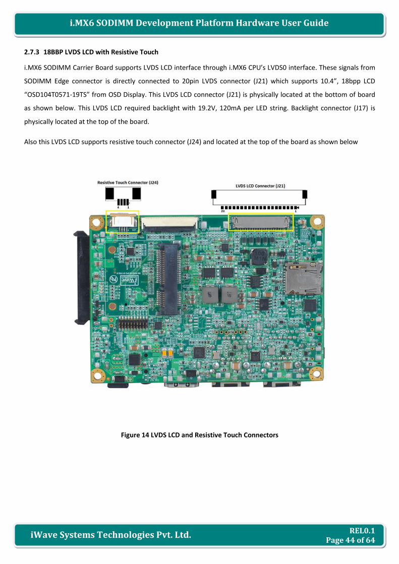
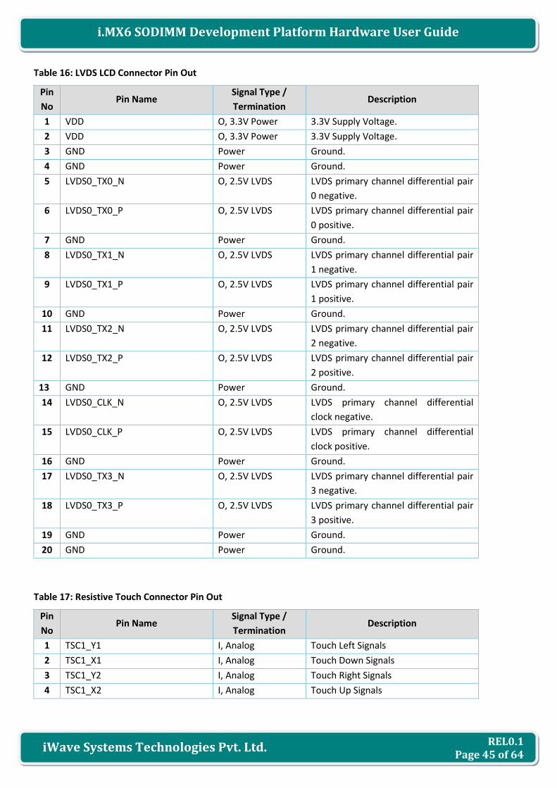
2.7.3 18BBP LVDS LCD with Resistive Touch
i.MX6 SODIMM Carrier Board supports LVDS LCD interface through i.MX6 CPU’s LVDS0 interface. These signals from
SODIMM Edge connector is directly connected to 20pin LVDS connector (J21) which supports 10.4”, 18bpp LCD
“OSD104T0571-19TS” from OSD Display. This LVDS LCD connector (J21) is physically located at the bottom of board
as shown below. This LVDS LCD required backlight with 19.2V, 120mA per LED string. Backlight connector (J17) is
physically located at the top of the board.
Also this LVDS LCD supports resistive touch connector (J24) and located at the top of the board as shown below
Figure 14 LVDS LCD and Resistive Touch Connectors
REL0.1 Page 45 of 64
iWave Systems Technologies Pvt. Ltd.
i.MX6 SODIMM Development Platform Hardware User Guide
Table 16: LVDS LCD Connector Pin Out
Pin
No Pin Name
Signal Type /
Termination Description
1 VDD O, 3.3V Power 3.3V Supply Voltage.
2 VDD O, 3.3V Power 3.3V Supply Voltage.
3 GND Power Ground.
4 GND Power Ground.
5 LVDS0_TX0_N O, 2.5V LVDS LVDS primary channel differential pair
0 negative.
6 LVDS0_TX0_P O, 2.5V LVDS LVDS primary channel differential pair
0 positive.
7 GND Power Ground.
8 LVDS0_TX1_N O, 2.5V LVDS LVDS primary channel differential pair
1 negative.
9 LVDS0_TX1_P O, 2.5V LVDS LVDS primary channel differential pair
1 positive.
10 GND Power Ground.
11 LVDS0_TX2_N O, 2.5V LVDS LVDS primary channel differential pair
2 negative.
12 LVDS0_TX2_P O, 2.5V LVDS LVDS primary channel differential pair
2 positive.
13 GND Power Ground.
14 LVDS0_CLK_N O, 2.5V LVDS LVDS primary channel differential
clock negative.
15 LVDS0_CLK_P O, 2.5V LVDS LVDS primary channel differential
clock positive.
16 GND Power Ground.
17 LVDS0_TX3_N O, 2.5V LVDS LVDS primary channel differential pair
3 negative.
18 LVDS0_TX3_P O, 2.5V LVDS LVDS primary channel differential pair
3 positive.
19 GND Power Ground.
20 GND Power Ground.
Table 17: Resistive Touch Connector Pin Out
Pin
No Pin Name
Signal Type /
Termination Description
1 TSC1_Y1 I, Analog Touch Left Signals
2 TSC1_X1 I, Analog Touch Down Signals
3 TSC1_Y2 I, Analog Touch Right Signals
4 TSC1_X2 I, Analog Touch Up Signals
REL0.1 Page 46 of 64
iWave Systems Technologies Pvt. Ltd.
i.MX6 SODIMM Development Platform Hardware User Guide
Table 18: LVDS1 Backlight Connector Pin Out
Pin
No Pin Name
Signal Type /
Termination Description
1 NC - -
2 NC - -
3 NC - -
4 NC - -
5 V_LED_K O, 190mV Power LED Cathode Voltage
6 V_LED_A O, 20V Power LED Anode Voltage
Note: To change the LVDS0 Backlight LED driver setting,
1. Change Current sensing resistor R191 (RSET) by calculating using the below formula
Where VFB = 190mV, ILED = Current required for LCD backlight LEDs.
2. Change D19 Zener Diode from 20V to required voltage.
(Populated diode part number is BZT52C20-7-F)
REL0.1 Page 47 of 64
iWave Systems Technologies Pvt. Ltd.
i.MX6 SODIMM Development Platform Hardware User Guide
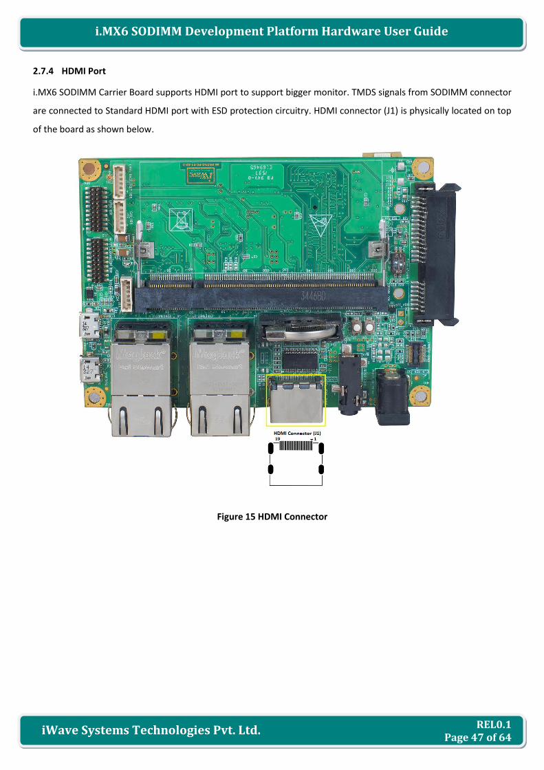
2.7.4 HDMI Port
i.MX6 SODIMM Carrier Board supports HDMI port to support bigger monitor. TMDS signals from SODIMM connector
are connected to Standard HDMI port with ESD protection circuitry. HDMI connector (J1) is physically located on top
of the board as shown below.
Figure 15 HDMI Connector

REL0.1 Page 48 of 64
iWave Systems Technologies Pvt. Ltd.
i.MX6 SODIMM Development Platform Hardware User Guide
Table 19: HDMI Connector Pin Out
Pin
No Pin Name
Signal Type /
Termination Description
1 HDMI_D2P O, TMDS HDMI data2 pair positive.
2 GND Power Ground.
3 HDMI_D2M O, TMDS HDMI data2 pair negative.
4 HDMI_D1P O, TMDS HDMI data1 pair positive.
5 GND Power Ground.
6 HDMI_D1M O, TMDS HDMI data1 pair negative.
7 HDMI_D0P O, TMDS HDMI data0 pair positive.
8 GND Power Ground.
9 HDMI_D0M O, TMDS HDMI data0 pair negative.
10 HDMI_CLKP O, TMDS HDMI Clock pair positive.
11 GND Power Ground.
12 HDMI_CLKM O, TMDS HDMI Clock pair negative.
13 GPIO1_IO21(SD1_DAT3) IO, 3.3V CMOS Consumer Electronic Control.
14 NC - -
15 I2C1_SCL(EIM_D21) O, 3.3V CMOS EDID I2C Clock.
16 I2C1_SDA(EIM_D28) IO, 3.3V CMOS EDID I2C Data
17 GND Power Ground.
18 O, 5V Power O, 5V Power 5V Supply Voltage.
19 HDMI_HPD I, 3.3V CMOS HDMI Cable Hot plug detect.
20 MH1, MH2, MH3, MH4 Mechanical
support
Mechanical support
REL0.1 Page 49 of 64
iWave Systems Technologies Pvt. Ltd.
i.MX6 SODIMM Development Platform Hardware User Guide
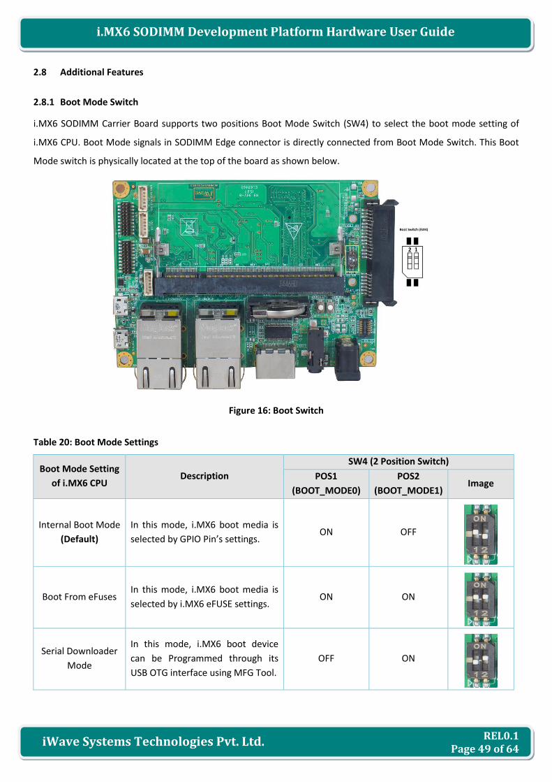
2.8 Additional Features
2.8.1 Boot Mode Switch
i.MX6 SODIMM Carrier Board supports two positions Boot Mode Switch (SW4) to select the boot mode setting of
i.MX6 CPU. Boot Mode signals in SODIMM Edge connector is directly connected from Boot Mode Switch. This Boot
Mode switch is physically located at the top of the board as shown below.
Figure 16: Boot Switch
Table 20: Boot Mode Settings
Boot Mode Setting
of i.MX6 CPU Description
SW4 (2 Position Switch)
POS1
(BOOT_MODE0)
POS2
(BOOT_MODE1) Image
Internal Boot Mode
(Default)
In this mode, i.MX6 boot media is
selected by GPIO Pin’s settings. ON OFF
Boot From eFuses In this mode, i.MX6 boot media is
selected by i.MX6 eFUSE settings. ON ON
Serial Downloader
Mode
In this mode, i.MX6 boot device
can be Programmed through its
USB OTG interface using MFG Tool.
OFF ON
REL0.1 Page 50 of 64
iWave Systems Technologies Pvt. Ltd.
i.MX6 SODIMM Development Platform Hardware User Guide
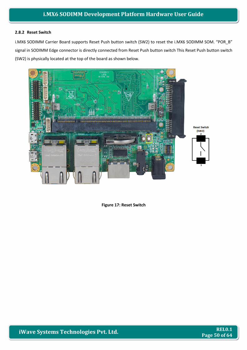
2.8.2 Reset Switch
i.MX6 SODIMM Carrier Board supports Reset Push button switch (SW2) to reset the i.MX6 SODIMM SOM. “POR_B”
signal in SODIMM Edge connector is directly connected from Reset Push button switch This Reset Push button switch
(SW2) is physically located at the top of the board as shown below.
Figure 17: Reset Switch
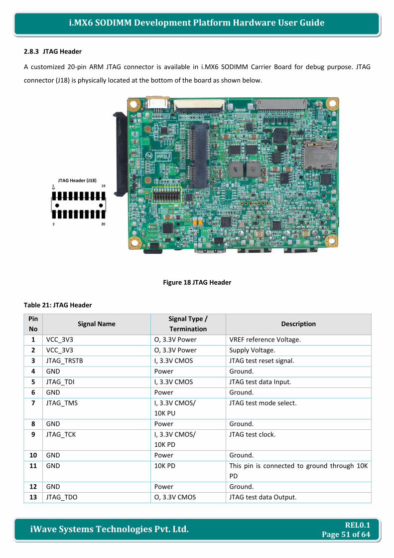
REL0.1 Page 51 of 64
iWave Systems Technologies Pvt. Ltd.
i.MX6 SODIMM Development Platform Hardware User Guide
2.8.3 JTAG Header
A customized 20-pin ARM JTAG connector is available in i.MX6 SODIMM Carrier Board for debug purpose. JTAG
connector (J18) is physically located at the bottom of the board as shown below.
Figure 18 JTAG Header
Table 21: JTAG Header
Pin
No Signal Name
Signal Type /
Termination Description
1 VCC_3V3 O, 3.3V Power VREF reference Voltage.
2 VCC_3V3 O, 3.3V Power Supply Voltage.
3 JTAG_TRSTB I, 3.3V CMOS JTAG test reset signal.
4 GND Power Ground.
5 JTAG_TDI I, 3.3V CMOS JTAG test data Input.
6 GND Power Ground.
7 JTAG_TMS I, 3.3V CMOS/
10K PU
JTAG test mode select.
8 GND Power Ground.
9 JTAG_TCK I, 3.3V CMOS/
10K PD
JTAG test clock.
10 GND Power Ground.
11 GND 10K PD This pin is connected to ground through 10K
PD
12 GND Power Ground.
13 JTAG_TDO O, 3.3V CMOS JTAG test data Output.

REL0.1 Page 52 of 64
iWave Systems Technologies Pvt. Ltd.
i.MX6 SODIMM Development Platform Hardware User Guide
14 GND Power Ground.
15 n_RST_OUT I,3.3V CMOS/
10K PU
Reset Signal.
16 GND Power Ground.
17 -
18 GND Power Ground.
19 GND 10K PD This pin is connected to ground through 10K
PD
20 GND Power Ground.
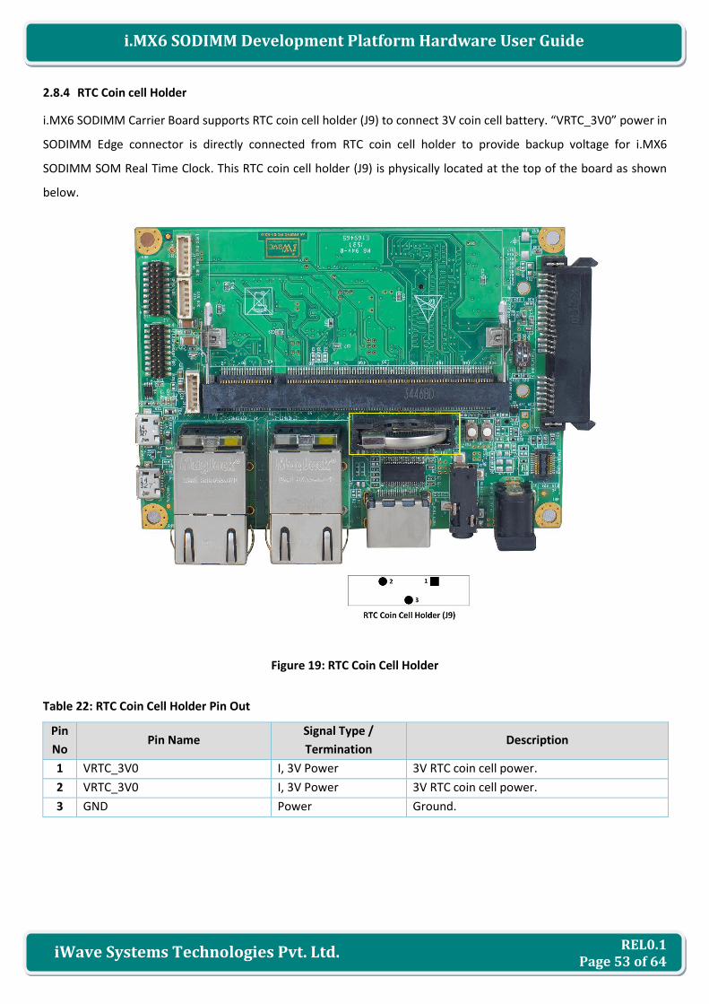
REL0.1 Page 53 of 64
iWave Systems Technologies Pvt. Ltd.
i.MX6 SODIMM Development Platform Hardware User Guide
2.8.4 RTC Coin cell Holder
i.MX6 SODIMM Carrier Board supports RTC coin cell holder (J9) to connect 3V coin cell battery. “VRTC_3V0” power in
SODIMM Edge connector is directly connected from RTC coin cell holder to provide backup voltage for i.MX6
SODIMM SOM Real Time Clock. This RTC coin cell holder (J9) is physically located at the top of the board as shown
below.
Figure 19: RTC Coin Cell Holder
Table 22: RTC Coin Cell Holder Pin Out
Pin
No Pin Name
Signal Type /
Termination Description
1 VRTC_3V0 I, 3V Power 3V RTC coin cell power.
2 VRTC_3V0 I, 3V Power 3V RTC coin cell power.
3 GND Power Ground.

REL0.1 Page 54 of 64
iWave Systems Technologies Pvt. Ltd.
i.MX6 SODIMM Development Platform Hardware User Guide
2.9 Expansion Header
i.MX6 SODIMM Carrier Board has one 20pin Expansion Header (J12) for unused interfaces expansion. Here unused
interfaces means, Interfaces which are supported in i.MX6 SODIMM SOM but unused in i.MX6 SODIMM Carrier
Board like CAN2, UART1 and UART4. These unused interfaces from SODIMM Edge connector is directly connected to
Expansion Header. This Expansion Header (J12) is physically located at the top of the board as shown below.
Figure 20: Expansion Header
REL0.1 Page 55 of 64
iWave Systems Technologies Pvt. Ltd.
i.MX6 SODIMM Development Platform Hardware User Guide
Table 23: Expansion Header Pin Out
Pin
No Signal Name
Signal Type /
Termination Description
1 VCC_5V O, 5V Power 5V Supply Voltage.
2 VCC_3V3 O, 3.3V Power 3.3V Supply Voltage.
3 UART4_TXD(KEY_COL0) O,3.3V CMOS UART4 Transmit Signal.
4 UART4_RXD(KEY_ROW0) I, 3.3V CMOS UART4 Receive Signal.
5 UART4_RTS_B(CSI0_DAT16) I, 3.3V CMOS UART4 Ready To Send Signal.
6 UART4_CTS_B(CSI0_DAT17) O,3.3V CMOS UART4 Clear To Send Signal.
7 CAN2_TX(KEY_COL4) O, 3.3V CMOS CAN2 Transmit Signal.
8 CAN2_RX(KEY_ROW4) I, 3.3V CMOS CAN2 Receive Signal.
9 UART1_TXD(SD3_DAT7) O, 3.3V CMOS UART1 Transmit Signal.
10 UART1_RXD(SD3_DAT6) I, 3.3V CMOS UART1 Receive Signal.
11 UART1_RTS_B(EIM_D20) I, 3.3V CMOS UART1 Ready To Send Signal.
12 UART1_CTS_B(EIM_D19) O,3.3V CMOS UART1 Clear To Send Signal.
13 eCSPI2_SCLK(CSI0_DAT8) O, 3.3V CMOS This signal is optionally connected to this pin
through resistor and default not populated.
14 eCSPI2_MISO(CSI0_DAT10) I, 3.3V CMOS This signal is optionally connected to this pin
through resistor and default not populated.
15 eCSPI2_MOSI(CSI0_DAT9) O, 3.3V CMOS This signal is optionally connected to this pin
through resistor and default not populated.
16 eCSPI2_SS2(EIM_D24) O, 3.3V CMOS SPI2 Chip select.
17 eCSPI2_SS1(EIM_LBA) O, 3.3V CMOS/ 10K PD
This signal is optionally connected to this pin
through resistor and default not populated.
18 PWM2_OUT(SD1_DAT2) O, 3.3V CMOS PWM2 output
19 GND Power Ground.
20 GND Power Ground.
.

REL0.1 Page 56 of 64
iWave Systems Technologies Pvt. Ltd.
i.MX6 SODIMM Development Platform Hardware User Guide
2.10 GPIO Header
i.MX6 SODIMM Carrier Board has one 20pin GPIO Header (J16) for unused GPIO pins. Six unused GPIO pins from
SODIMM Edge connector is directly connected to GPIO Header. This GPIO Header (J16) is physically located at the
top of the board as shown below.
Figure 21: GPIO Header
REL0.1 Page 57 of 64
iWave Systems Technologies Pvt. Ltd.
i.MX6 SODIMM Development Platform Hardware User Guide
Table 24: GPIO Header Pin Out
Pin
No Signal Name
Signal Type /
Termination Description
1 VCC_5V O, 5V Power 5V Supply Voltage.
2 VCC_3V3 O, 3.3 Power 3.3V Supply Voltage.
3 DISP0_DAT0 IO,3.3V CMOS General Purpose Input/Output.
4 DISP0_DAT1 IO,3.3V CMOS General Purpose Input/Output.
5 DISP0_DAT8 IO,3.3V CMOS General Purpose Input/Output.
6 DISP0_DAT9 IO,3.3V CMOS General Purpose Input/Output.
7 DISP0_DAT16 IO,3.3V CMOS General Purpose Input/Output.
8 DISP0_DAT17 IO,3.3V CMOS General Purpose Input/Output.
9 USB_OTG_CHD_B - USB OTG Charge detect signal.
10 AUD4_RXC(SD2_CMD) I, 3.3V CMOS Audio receive clock
11 AUD4_RXFS(SD2_CLK) I, 3.3V CMOS Audio receive frame synchronization
12 GPIO4_IO20(DI0_PIN4) IO,3.3V CMOS General Purpose Input/Output.
13 GPIO6_IO00(CSI0_DAT14) IO,3.3V CMOS General Purpose Input/Output.
14 GPIO4_IO12(KEY_COL3) IO,3.3V CMOS General Purpose Input/Output.
15 GPIO4_IO11(KEY_ROW2) - IO,3.3V CMOS
16 NC - Default NC.
Note: This pin is connected SODIMM Edge pin
189.
17 NC - Default NC.
Note: This pin is connected SODIMM Edge pin
194.
18 NC - Default NC.
Note: This pin is connected SODIMM Edge pin
196.
19 GND Power Ground.
20 GND Power Ground.
2.11 Optional Features
i.MX6 SODIMM Carrier Board has PCB footprint option for some features which are not supported by default. These
optional features are explained in the following sections.
To add any of these optional features in i.MX6 SODIMM Carrier Board, please contact iWave.
2.11.1 RTC Controller
i.MX6 SODIMM Carrier Board optionally supports RTC Controller “BQ32000DR” on board. This RTC Controller is
connected to the i.MX6 CPU through I2C3 Interface and operates at 3.3V voltage level. Backup voltage for this RTC
controller is connected from RTC coin holder. This is the optional feature and not be populated by default.
REL0.1 Page 58 of 64
iWave Systems Technologies Pvt. Ltd.
i.MX6 SODIMM Development Platform Hardware User Guide
3. TECHNICAL SPECIFICATION
This section provides detailed information about the i.MX6 SODIMM Carrier Board technical specification with
Electrical, Environmental and Mechanical characteristics.
3.1 Electrical Characteristics
3.1.1 Power Input Requirement
The i.MX6 SODIMM Carrier Board is designed to work with a +5V external power and uses on board voltage
regulators for internal power management. 5V power input from an external power supply is connected to the
SODIMM Carrier Board through Power Jack (J2). This 1.3mm x 3.8mm barrel connector Jack should fit standard DC
Plugs with an inner dimension of 1.35mm and an outer dimension of 3.5mm. This connector is physically placed at
the top of the board as shown below.
Figure 22: Power Jack
Table 25: Power Jack Pin Out
Pin
No Signal Name
Signal Type /
Termination Description
1 VCC 5V, Power Input Supply Voltage.
2 GND Power Ground.
3 GND Power Ground.
REL0.1 Page 59 of 64
iWave Systems Technologies Pvt. Ltd.
i.MX6 SODIMM Development Platform Hardware User Guide
The below table provides the Power Input Requirement of i.MX6 SODIMM Carrier Board.
Table 26: Power Input Requirement
Sl. No. Power Rail Min (V) Typical (V) Max(V) Max Input Ripple
1 VCC_5V¹ 4.75V 5V 5.25V ±50mV
2 VRTC_3V0² 2.8V 3V 3.3V ±20 mV
¹ i.MX6 SODIMM Carrier Board is designed to work with 5V, 1A input power from External Power Adapter.
² This voltage is from Coin cell holder and used as backup power source in RTC of i.MX6 SODIMM SOM when VCC is
off. This is an optional power and required only if RTC functionality is used.
Important Note: All carrier board power supplies should be powered ON only after the i.MX6 CPU is powered ON
completely in the i.MX6 SODIMM SOM. This is to ensure that there is no back voltage (leakage) from any supply on
the board towards the i.MX6 CPU IO pins.
REL0.1 Page 60 of 64
iWave Systems Technologies Pvt. Ltd.
i.MX6 SODIMM Development Platform Hardware User Guide
3.2 Environmental Characteristics
3.2.1 Environmental Specification
The below table provides the Environment specification of i.MX6 SODIMM Carrier Board.
Table 27: Environmental Specification
Parameters Min Max
Operating temperature range (Commercial)¹ 0°C 60°C
Storage temperature range 0°C 60°C
¹ iWave only guarantees the component selection for the given operating temperature.
3.2.2 RoHS Compliance
iWave’s i.MX6 SODIMM Carrier Board is designed by using RoHS compliant components and manufactured on lead
free production process.
3.2.3 Electrostatic Discharge
iWave’s i.MX6 SODIMM Carrier Board is sensitive to electro static discharge and so high voltages caused by static
electricity could damage some of the devices on board. It is packed with necessary protection while shipping. Do not
open or use the Carrier Board except at an electrostatic free workstation.

REL0.1 Page 61 of 64
iWave Systems Technologies Pvt. Ltd.
i.MX6 SODIMM Development Platform Hardware User Guide
3.3 Mechanical Characteristics
3.3.1 i.MX6 SODIMM Carrier Board Mechanical Dimensions
i.MX6 SODIMM Carrier Board PCB size is 100mm x 72mm x 1.6mm. SODIMM Carrier Board mechanical dimension is
shown below. Please refer the JEDEC Physical standard DDR S.O.DIMM specification for SODIMM Edge connector
mechanical details.
Figure 23: Mechanical dimension of i.MX6 SODIMM Carrier Board
i.MX6 SODIMM Carrier Board PCB thickness is 1.6mm±0.1mm, top side maximum height component is Ethernet Jack
1 & 2 (23.24mm) followed by RTC Battery Holder (21.9mm) and bottom side maximum height component is JTAG
Header (5mm) followed by Power Inductor (3mm). Please refer the below figure for height details of the i.MX6
SODIMM Carrier Board.
Figure 24: Mechanical dimension of i.MX6 SODIMM Carrier Board - Side View

REL0.1 Page 62 of 64
iWave Systems Technologies Pvt. Ltd.
i.MX6 SODIMM Development Platform Hardware User Guide
4. ORDERING INFORMATION
The below table provides the standard orderable part numbers for i.MX6 Development Platform which includes
i.MX6 SODIMM SOM and SODIMM carrier board. If the desired part number is not listed in below table, or if any
custom configuration part number is required, please contact iWave.
Table 28: Orderable Product Part Numbers
Product Part Number Description Temperature
iW-G15D-SM04-3D001G-E004G-LCA i.MX6 Quad SODIMM SOM Linux Development Kit with
4.3" resistive touch LCD Display.
Commercial
iW-G15D-SM04-3D001G-E004G-ACA i.MX6 Quad SODIMM SOM Android Development Kit with
4.3" resistive touch LCD Display.
Commercial
iW-G15D-SM04-3D001G-E004G-LCB i.MX6 Quad SODIMM SOM Linux Development Kit
without LCD Display.
Commercial
iW-G15D-SM04-3D001G-E004G-ACB i.MX6 Quad SODIMM SOM Android Development Kit
without LCD Display.
Commercial
Note: For Development platform identification purpose, Product part number is pasted as Label with Barcode
readable format.
Note: For other i.MX6 CPU variant supported SODIMM Development Kit part number, please contact iWave.
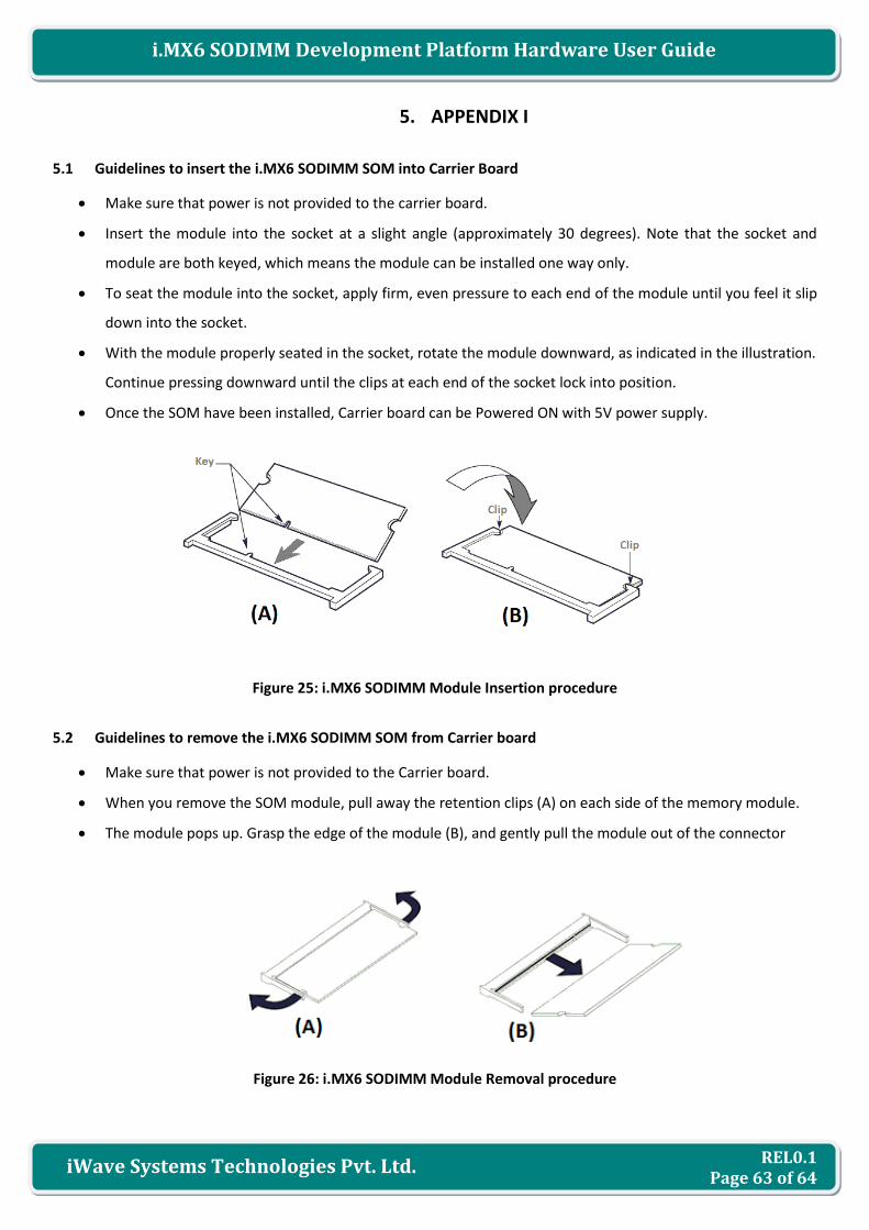
REL0.1 Page 63 of 64
iWave Systems Technologies Pvt. Ltd.
i.MX6 SODIMM Development Platform Hardware User Guide
5. APPENDIX I
5.1 Guidelines to insert the i.MX6 SODIMM SOM into Carrier Board
Make sure that power is not provided to the carrier board.
Insert the module into the socket at a slight angle (approximately 30 degrees). Note that the socket and
module are both keyed, which means the module can be installed one way only.
To seat the module into the socket, apply firm, even pressure to each end of the module until you feel it slip
down into the socket.
With the module properly seated in the socket, rotate the module downward, as indicated in the illustration.
Continue pressing downward until the clips at each end of the socket lock into position.
Once the SOM have been installed, Carrier board can be Powered ON with 5V power supply.
Figure 25: i.MX6 SODIMM Module Insertion procedure
5.2 Guidelines to remove the i.MX6 SODIMM SOM from Carrier board
Make sure that power is not provided to the Carrier board.
When you remove the SOM module, pull away the retention clips (A) on each side of the memory module.
The module pops up. Grasp the edge of the module (B), and gently pull the module out of the connector
Figure 26: i.MX6 SODIMM Module Removal procedure

REL0.1 Page 64 of 64
iWave Systems Technologies Pvt. Ltd.
i.MX6 SODIMM Development Platform Hardware User Guide