Embed Size (px)
Citation preview
IMAGE PROCESSING
Group 3 Final Report for
COLOUR IMAGE PROCESSING SYSTEM
System that manipulates pixel information of images taken by a serial camera
Kwan Yin Lau, Xiang Gao, and Jun Zhao
Abstract
According to IDC, the worldwide smartphone shipments top one billion in 2013 [1]. Although climbing fast, the
number of photos taken by smartphone is still low compared to regular cameras [2]. This shows that many
people are still not confident about the image quality of the photos taken by their smartphones. In this document
we propose an intermediate solution to the problem: a simple digital camera implementation with web-based
image editor.
Using the system, one can use the web-based editor directly on their mobile devices’ browser to retrieve the
image from the camera and perform specified image processing operations on the image. Instead of using the
camera of the mobile device, one can just use his or her regular camera. This allows people to get better image
quality. The types of image processing are to be discussed first in this document in order to present the main
functionalities of this system. Hardware design will be implemented using FPGA as an embedded system to
interface all hardware and software components required to do image processing. The external hardwares
include a camera used to capture images, a VGA monitor to display the image, and a router as the connection
between the DE2 board and the client side. This system is able to perform colour image processing as well as
grayscale image processing. The processed image can be displayed on a VGA screen, as well as on the client’s
web browser. Some future works include allowing users to save the image to a SD card, and hardware
acceleration using custom VHDL modules.
Table of contents
Abstract
1. Functional Requirements of Project
2. Design and Description of Operation
2.1 User interface module design
2.2 C328 camera: Camera command module and camera driver module design
2.3 D5M camera: Camera driver module design
2.4 D5M camera: Colour to Greyscale conversion and Edge Detection module Streaming design
2.5 VGA Streaming module design
2.6 Web editor/Ethernet module design
2.7 Web editor Colour to Greyscale conversion and Edge Detection Signal design
2.8 Web editor Get Image module design
2.9 Image controller module design
2.10 Image processor module design
3. Bill of Materials
4. Reusable Design Units
5. Datasheet
6. Background Reading
7. Software design
8. Test Plan
9. Results of Experiments and Characterization
9.1 Simulation Result of Ageing Effect Algorithm
9.2 Comparison of Image Operations Using Software and Hardware Implementation
9.3 Comparison of C328 camera and D5M camera
10. Safety
12. Sustainability
13. References
Appendices
A. Quick start manual
B. Future work
C. Hardware documentation
D. Source code
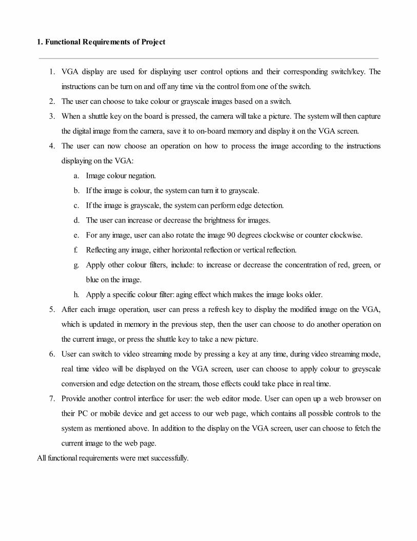
1. Functional Requirements of Project
1. VGA display are used for displaying user control options and their corresponding switch/key. The
instructions can be turn on and off any time via the control from one of the switch.
2. The user can choose to take colour or grayscale images based on a switch.
3. When a shuttle key on the board is pressed, the camera will take a picture. The system will then capture
the digital image from the camera, save it to on-board memory and display it on the VGA screen.
4. The user can now choose an operation on how to process the image according to the instructions
displaying on the VGA:
a. Image colour negation.
b. If the image is colour, the system can turn it to grayscale.
c. If the image is grayscale, the system can perform edge detection.
d. The user can increase or decrease the brightness for images.
e. For any image, user can also rotate the image 90 degrees clockwise or counter clockwise.
f. Reflecting any image, either horizontal reflection or vertical reflection.
g. Apply other colour filters, include: to increase or decrease the concentration of red, green, or
blue on the image.
h. Apply a specific colour filter: aging effect which makes the image looks older.
5. After each image operation, user can press a refresh key to display the modified image on the VGA,
which is updated in memory in the previous step, then the user can choose to do another operation on
the current image, or press the shuttle key to take a new picture.
6. User can switch to video streaming mode by pressing a key at any time, during video streaming mode,
real time video will be displayed on the VGA screen, user can choose to apply colour to greyscale
conversion and edge detection on the stream, those effects could take place in real time.
7. Provide another control interface for user: the web editor mode. User can open up a web browser on
their PC or mobile device and get access to our web page, which contains all possible controls to the
system as mentioned above. In addition to the display on the VGA screen, user can choose to fetch the
current image to the web page.
All functional requirements were met successfully.
2. Design and Description of Operation
Figure 2a : System Component
Operation flow
● VGA: display user instruction interface. Example options are “KEY3: Take a Picture”, “KEY2: Refresh
Image”, “KEY1: Video mode”, “SW0 ON: Colour”, “SW0 OFF: GrayScale”, “SW1 ON:
Invert/Negate”, “SW8 ON: To GrayScale”, “SW2 ON: Change Brightness”, “SW3 ON: Increase”,
“SW3 OFF: decrease”, etc.
1. Web server startup, display server IP address on LCD.
2. Start up the system, initialize all parts, display user options on VGA screen, System will be running in
video streaming mode. Frames are displayed on VGA.
3. Under video streaming mode, Switch 0 is used to choose from colour mode and grayscale mode, when
in grayscale mode, Switch 8 is used to turn on edge detection.
4. When key3 on board is pressed, send a signal through PIO, camera driver to off board camera to take
a grayscale or colour or edge detection picture according to switch 0 and switch 8.
5. Use ribbon cable to pass the image through GPIO, and save the image to SDRAM which is the image
buffer, output the image to VGA screen.
6. When key1 is press, switch from Snapshot mode back to Video streaming mode.
7. When key2 is press for refresh image, check user image operation option on switch. No operation will
be done if option is not applicable (such as to convert a grayscale image to grayscale)
8. Only when switch 2 (for change brightness) is on, switch 3 (increase/decrease) will take effect on next
refresh. Similarly, only when switch 4 (for rotation) is on, switch 5 (clockwise / counter clockwise) will
take effect on next refresh.
9. When image operation is applicable with image on refresh, load corresponding image processing
software from flash.
10. Perform image processing operation, display the output on VGA, store the output back to SDRAM.
Figure 2b : Functional modules
Image operations basic concepts
From the camera user manual [4], preferred image output formats are: 8-bit grayscale in Y only and 16-bit
colour in RGB565. For 16-bit RGB, its colour model is bits 15-11 for red, bits 10-5 for green, and bits 4-0 for
blue. Also when a pixel is smaller, it is closer to black. When a pixel is larger, it is closer to white. So in
grayscale, 0x00 is black and 0xFF is white. For colour, 0x0000 is black while 0xFFFF is white [11]. Image
operation functions are develop base on the idea above, for example: The increase/decrease in brightness can
be implemented in adjusting the pixel closer to white or closer to black. To invert a grayscale pixel or to negate
a colour pixel, just subtract the current value from the largest value (0xFF or 0xFFFF).
The module of RGB Resampler / Colour space converter is the built-in hardware in Altera Video IP core that
can do the 16-bit RGB colour to 8-bit grayscale conversion [13].
2.1 User interface module design
This module consist of the 16x2 LCD controller, differents parallel input/output (PIO) components, and also the
VGA character buffer component. The LCD is used to display the current user action, for example: take a
picture, refresh image, or switch to video mode, etc. The hardware abstraction layer (HAL) functions from
Altera University Program is used [12].
The keypads on DE2 board (ie: key 1 to key 3) are interfaced using PIO module which enables the input
interrupt functionality. When one of the keys are pressed, the PIO for the keys would capture the raising edge
of the key signal, then it would generate an interrupt which could be handle by the interrupt service routine
written in software. The ISR would read the corresponding edge capture register to determine which key was
pressed and pass a message to other modules.
The switches on the DE2 board are for the user to interface with the system, for example choosing the image
colour type, choosing an image operation to perform, etc. All switches that represents user options are
controlled by PIO input component. When the system detects that the refresh key was pressed, the PIO data
registers for the switches would be read to determine which switch(es) are turned on.
Another functional component using PIO was a switch that turns on and off user instruction displaying on the
VGA screen. That switch is using PIO with interrupt module, which captures both raising and falling edge on the
switch signal.
The last part of user interface module was the user instruction display on the VGA screen using the module of
VGA character buffer with dma. This module also controlled by the altera HAL functions. To display a line of
instruction on the VGA screen, we should write a string using the alt_up_char_buffer_string() function that also
have the x and y coordinate on the screen as parameters. More hardware configuration related to VGA display
are discuss in VGA module design below.
2.2 C328 camera: Camera command module and camera driver module design
In order to interface and use the camera (C328 UART camera, for detail refer to Reference) to take picture. A
camera driver and a camera command module is needed. The C328 camera can be controlled using binary
commands, every command consist of six bytes. The first byte is the command prefix which is always fixed as
0xAA. The second byte was the command ID that tells the command type. Other bytes are the command
parameters that differs for each command. Details of the command can be consult from the C328 camera user
manual [4]. The camera command module defines the hexadecimal symbolic constants for the camera
commands. Set methods are provided from the module to form a valid camera command.
The camera driver module connects the camera and general purpose input/output (GPIO) port via the RS232
UART module from Altera University Program [24]. RS232 UART was able to transfer 8-bit binary (a
character) in read or a write using the HAL functions of alt_up_rs232_write_data() and
alt_up_rs232_read_data(). There is build-in read FIFO buffer and write FIFO buffers in RS232 UART
module. Before every read, we need to make sure there are bytes ready to read in read FIFO by calling
alt_up_rs232_get_used_space_in_read_FIFO(). Similarly, before a write, we need to make sure there is
enough space in write FIFO by calling alt_up_rs232_get_available_space_in_write_FIFO(). The camera driver
read and write camera command from the camera command module byte by byte through the RS232 UART.
All bytes of image taken from the camera are also transfer via UART.
When the system startup, the camera driver first required to make connection with the C328 camera by
synchronizing with it. The driver will send up to 60 SYNC command to the camera until it gets back an ACK
command. In order to take a picture using the camera, the driver should go through a series of steps, in other
words, sending different command to the camera, after each command is sent, the driver have to wait for the
corresponding ACK from the camera. First, initialize the camera to set up the image type (grayscale or colour)
and image resolution using the INITIAL command. Next, take a snapshot of a uncompressed or a compressed
picture using the SNAPSHOT command. The camera will then inform the driver which type of image was taken
and its size via the DATA command. Then the content of the image taken would be transfer byte by byte to the
driver. After the last byte was received, the driver needs to ACK to the camera [4].
Every bytes of the image from the camera is written to an image buffer which is actually a character (8-bit
binary) array. And the image buffer is stored in the SDRAM, it is a shared memory between the camera driver
and the image controller.
2.3 D5M camera: Camera driver module design
The D5M camera provides a GPIO interface which can directly output the image data to SRAM on the DE2
board using the system bus, and it also has a well designed driver and video decoder from the Altera University
Program. In order to connect the camera with our system, two Altera University Program IP core are required.
The Altera Audio/Video Configuration Core for DE-Series Boards (config core)[9] are used to write and read
to the registers in the D5M camera in order to control it. The signals from the config core should connected to
SDATA and SCLK pins from the camera GPIO port as follow:
av_config_external_interface_SDAT => GPIO_1(23),
av_config_external_interface_SCLK => GPIO_1(24),
The Altera Video-in Decoder core from Altera Video IP Cores for Altera DE Series Boards[13] are used to
convert the raw data output from the D5M camera to Avalon Streaming Source. The signals from the Video-in
Decoder core should connected to PIXCLK, LVAL, FVAL, and D0 to D11 pins from the camera GPIO port
as follow:
video_in_decoder_external_interface_PIXEL_CLK => GPIO_1(0),
video_in_decoder_external_interface_LINE_VALID => GPIO_1(21),
video_in_decoder_external_interface_FRAME_VALID=> GPIO_1(22),
video_in_decoder_external_interface_PIXEL_DATA(0) => GPIO_1(13),
video_in_decoder_external_interface_PIXEL_DATA(1) => GPIO_1(12),
video_in_decoder_external_interface_PIXEL_DATA(2) => GPIO_1(11),
video_in_decoder_external_interface_PIXEL_DATA(3) => GPIO_1(10),
video_in_decoder_external_interface_PIXEL_DATA(4) => GPIO_1(9),
video_in_decoder_external_interface_PIXEL_DATA(5) => GPIO_1(8),
video_in_decoder_external_interface_PIXEL_DATA(6) => GPIO_1(7),
video_in_decoder_external_interface_PIXEL_DATA(7) => GPIO_1(6),
video_in_decoder_external_interface_PIXEL_DATA(8) => GPIO_1(5),
video_in_decoder_external_interface_PIXEL_DATA(9) => GPIO_1(4),
video_in_decoder_external_interface_PIXEL_DATA(10) => GPIO_1(3),
video_in_decoder_external_interface_PIXEL_DATA(11) => GPIO_1(1),
The external clock of D5M camera XCLKIN can be connected to the 50 MHz system clock source directly:
GPIO_1(16) <= CLOCK_50;
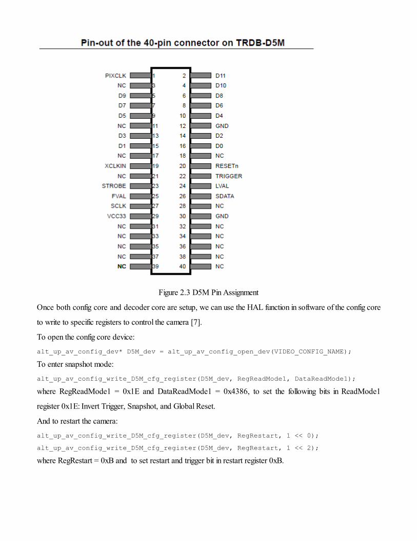
Figure 2.3 D5M Pin Assignment
Once both config core and decoder core are setup, we can use the HAL function in software of the config core
to write to specific registers to control the camera [7].
To open the config core device:
alt_up_av_config_dev* D5M_dev = alt_up_av_config_open_dev(VIDEO_CONFIG_NAME);
To enter snapshot mode:
alt_up_av_config_write_D5M_cfg_register(D5M_dev, RegReadMode1, DataReadMode1);
where RegReadMode1 = 0x1E and DataReadMode1 = 0x4386, to set the following bits in ReadMode1
register 0x1E: Invert Trigger, Snapshot, and Global Reset.
And to restart the camera:
alt_up_av_config_write_D5M_cfg_register(D5M_dev, RegRestart, 1 << 0);
alt_up_av_config_write_D5M_cfg_register(D5M_dev, RegRestart, 1 << 2);
where RegRestart = 0xB and to set restart and trigger bit in restart register 0xB.
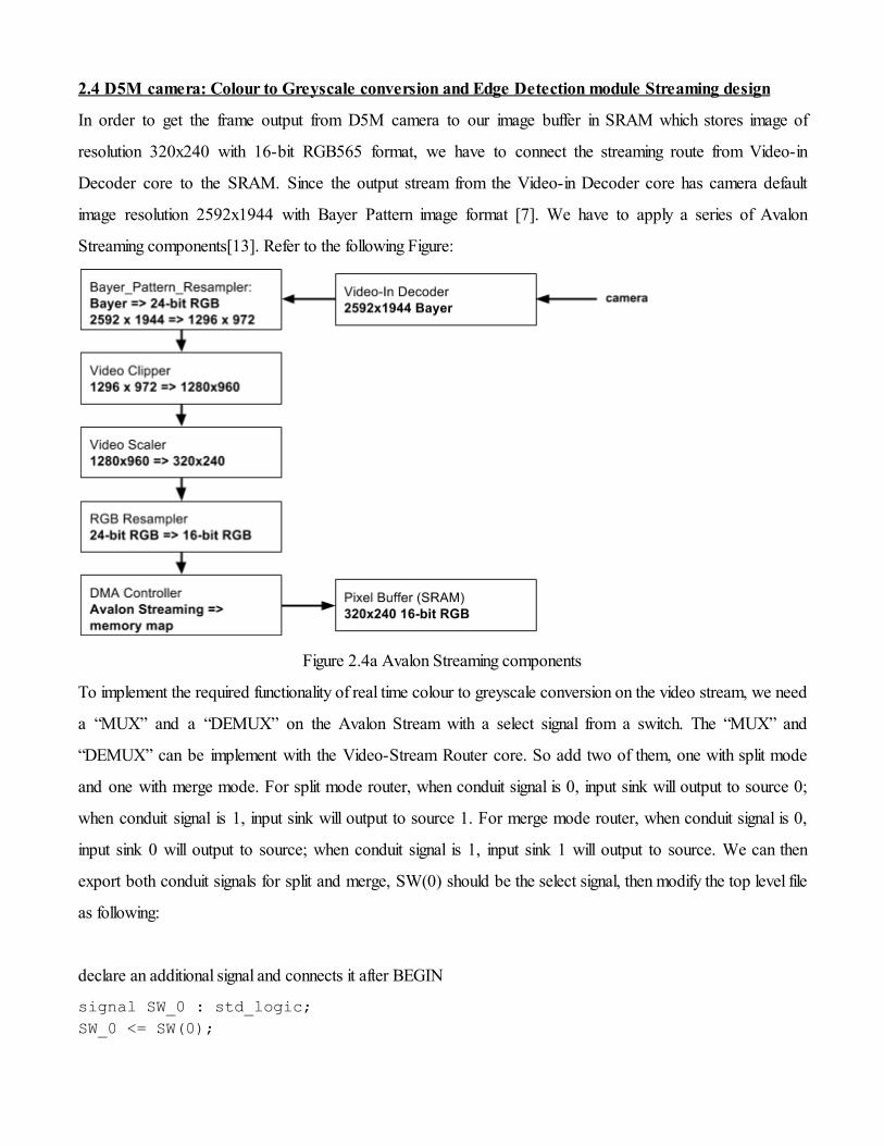
2.4 D5M camera: Colour to Greyscale conversion and Edge Detection module Streaming design
In order to get the frame output from D5M camera to our image buffer in SRAM which stores image of
resolution 320x240 with 16-bit RGB565 format, we have to connect the streaming route from Video-in
Decoder core to the SRAM. Since the output stream from the Video-in Decoder core has camera default
image resolution 2592x1944 with Bayer Pattern image format [7]. We have to apply a series of Avalon
Streaming components[13]. Refer to the following Figure:
Figure 2.4a Avalon Streaming components
To implement the required functionality of real time colour to greyscale conversion on the video stream, we need
a “MUX” and a “DEMUX” on the Avalon Stream with a select signal from a switch. The “MUX” and
“DEMUX” can be implement with the Video-Stream Router core. So add two of them, one with split mode
and one with merge mode. For split mode router, when conduit signal is 0, input sink will output to source 0;
when conduit signal is 1, input sink will output to source 1. For merge mode router, when conduit signal is 0,
input sink 0 will output to source; when conduit signal is 1, input sink 1 will output to source. We can then
export both conduit signals for split and merge, SW(0) should be the select signal, then modify the top level file
as following:
declare an additional signal and connects it after BEGIN
signal SW_0 : std_logic;
SW_0 <= SW(0);
add these connections to port map
switches_external_connection_export(0)=> SW_0,
color_gray_merge_external_interface_export => SW_0,
color_gray_split_external_interface_export => SW_0,
Between the two Video-Stream Router, to change the input stream from colour to greyscale, Colour-Space
Converter core is used. we use 24-bit RGB to Y. After that, use RGB resampler to set the format back to the
current one in the stream which is 24-bit RGB.
It is very similar to add the edge detection core to the current stream, since the edge detection core only applies
on grayscale stream, we can add a pair of split/merge Video-Stream Router between the Colour-Space
Converter core and RGB resampler core mentioned above for grayscale. At last, just insert the Edge Detection
core between the new Video-Stream routers. The following Figure shows the whole streaming flow from the
Video-In Decoder to the SRAM with colour to greyscale conversion and edge detection function added.
Figure 2.4b Avalon Streaming components with Video-Stream Routers
Of course we need to port map the new Video-Stream Router to switch 8.
signal SW_8 : std_logic;
SW_8 <= SW(8);
switches_external_connection_export(0)=> SW_8,
edge_detect_merge_external_interface_export => SW_8,
edge_detect_split_external_interface_export => SW_8,
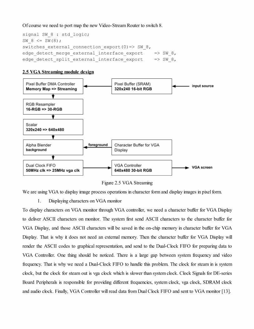
2.5 VGA Streaming module design
Figure 2.5 VGA Streaming
We are using VGA to display image process operations in character form and display images in pixel form.
1. Displaying characters on VGA monitor
To display characters on VGA monitor through VGA controller, we need a character buffer for VGA Display
to deliver ASCII characters on monitor. The system first send ASCII characters to the character buffer for
VGA Display, and those ASCII characters will be saved in the on-chip memory in character buffer for VGA
Display. That is why it does not need an external memory. Then the character buffer for VGA Display will
render the ASCII codes to graphical representation, and send to the Dual-Clock FIFO for preparing data to
VGA Controller. One thing should be noticed. There is a large gap between system frequency and video
frequency. That is why we need a Dual-Clock FIFO to handle this problem. The clock for steam in is system
clock, but the clock for steam out is vga clock which is slower than system clock. Clock Signals for DE-series
Board Peripherals is responsible for providing different frequencies, system clock, vga clock, SDRAM clock
and audio clock. Finally, VGA Controller will read data from Dual Clock FIFO and sent to VGA monitor [13].
Basic Algorithms:
1) Find the device Character Buffer from the device list and open it
char_buf_dev = alt_up_char_buffer_open_dev("/dev/VGA_Char_Buffer_With_DMA");
If the return value of char_buf_dev is not NULL, then the device was opened successfully. If
not, then error occurred.
2) Initial the device (optional)
alt_up_char_buffer_init(char_buf_dev);
3) Clear the screen
alt_up_char_buffer_clear(char_buf_dev);
4) Display strings on VGA monitor
alt_up_char_buffer_string(char_buf_dev, strings, x_position, y_position);
Strings: the characters will be displayed on monitor.
x_position and y_position: position where to display the strings.
2. Displaying images on VGA monitor
The pixel is the fundamental unit of digital image. Displaying an image can be considered as outputting every
pixel on monitor. The “size” of pixels refers to resolution. The VGA monitor supports 30 bit per pixel
representation and 640*480 resolutions as standard in this project. The images which will be displayed on the
monitor should be converted in the right form which is 30 bit per pixel and 640*480 resolutions.
2.a Displaying colour images on VGA monitor
For colour images, they are represented and stored in 16 RGB bit in memory. Unlike character buffer for VGA
display, pixel buffer DMA Controller does not contain memory inside, so external memory is needed. In this
project, SRAM and SDRAM are accessed by pixel buffer DMA Controller. After reading the pixel data from
external memory by pixel buffer DMA Controller, the pixel format should be converted from 16 bit RGB colour
space to 30 bit RGB colour space by RGB Resampler. Then the frame resolution should be converted from
320*240 to 640*480 by Scalar to be compliant with VGA Controller. In this project, colour images and
grayscale images are both needed [13].
2.b Displaying grayscale images on VGA monitor
The similarity between displaying colour images and grayscale images is converting to the right formation which
is 30 RGB bit and 640*480 resolutions. However, multiple differences should be considered. Grayscale images
are saved in 8 bit grayscale colour space in memory. Before using RGB Resampler as what we do on colour
images, an extra step is needed. Pixel buffer DMA Controller will send 8 bit grayscale data to colour space
converter which is used to convert grayscale to 24 bit RGB colour space. Then the next steps are much similar
with doing colour images, using RGB Resampler to convert 24 bit RGB format to 30 bit RGB format, using
Scaler to convert 320*240 frame resolutions to 640*480 resolutions [13].
Basic Algorithms:
1) Open both colour Pixel Buffer Controller and grayscale Pixel Buffer Controller
colour_pixel_buf_dev = alt_up_pixel_buffer_dma_open_dev(
"/dev/colour_Pixel_Buffer_DMA_Controller");
gray_pixel_buf_dev = alt_up_pixel_buffer_dma_open_dev(
"/dev/GrayScale_Pixel_Buffer_DMA_Controller");
If the return value of colour_pixel_buf_dev and gray_pixel_buf_dev are not NULL, then the
two devices were opened successfully. If not, then errors occurred.
2) Pixel Buffer Controller has two buffers, primary buffer and back buffer. Primary buffer stores
data which will be directly displayed on screen. Back buffer will save the next displaying pixel
data in advance, and then swap the data to primary buffer to be displayed on monitor. Back
buffer is used to increase the display speed. In order to increase the speed, we always save
pixel values in back buffer, then swap to primary buffer. Functions are provided to swap the
two buffers. At the beginning, make sure data will be sent to back buffer for colour and
grayscale Pixel Buffer Controllers.
alt_up_pixel_buffer_dma_change_back_buffer_address(gray_pixel_buf_dev,GRAY_BUF
FER);
alt_up_pixel_buffer_dma_change_back_buffer_address(colour_pixel_buf_dev,
COLOUR_BUFFER);
3) Clear the two buffers, parameter ‘1’ means back buffer, parameter ‘0’ means primary buffer.
alt_up_pixel_buffer_dma_clear_screen(gray_pixel_buf_dev, 0);
alt_up_pixel_buffer_dma_clear_screen(colour_pixel_buf_dev, 0);
alt_up_pixel_buffer_dma_clear_screen(gray_pixel_buf_dev, 1);
alt_up_pixel_buffer_dma_clear_screen(colour_pixel_buf_dev, 1);
4) Draw pixels on monitor.
alt_up_pixel_buffer_dma_draw(gray_pixel_buf_dev, colour_8, x,y);
alt_up_pixel_buffer_dma_draw(colour_pixel_buf_dev, colour_16, x,y);
colour_8: pixels are represented in 8 bit in grayscale mode.
colour_16: pixels are represented in 16 bit in colour mode.
x,y: positions where to display.
2.c Displaying both characters and images on VGA monitor
We need another component alpha blender to display both characters and images concurrently on VGA
monitor. Alpha blender always takes character data as foreground streaming and pixels data as background
streaming. The character buffer module need to be set as transparent to be the foreground. The Alpha blender
will combine the two streaming to one. And then alpha blender will send the one combined stream to Dual
Clock FIFO, which the input stream clock is the system clock while the output stream clock is the VGA clock.
Finally, VGA Controller will read data from Dual Clock FIFO and send them to VGA monitor. One thing to be
noted, VGA Controller is running at VGA clock [13].
2.6 Web editor/Ethernet module design
1. DM9000A Ethernet Controller
1.1 Qsys
In order to get Ethernet connection, Ethernet controller should be first implemented on the DE2 board.
The DE2 board uses Davicom DM9000A Fast Ethernet Controller. According to the DM9000A user manual
[20], the Ethernet Controller contains a SRAM, a MAC unit, PHY transceiver and an interface. Terasic
provides the HDL and TCL files to help us add the controller as a new component in Qsys. One thing should be
mentioned that DM9000A Ethernet Controller must be running at 25 MHZ clock. The conduit signal under the
DM9000A should be exported. A web server is running on FLASH memory, so three additional components
should be added in Qsys: generic_tristate_controller, tristate_conduit_bridge and tristate_conduit_pin_sharer.
The conduit signal under tristate_conduit_bridge should be exported. The Ethernet Controller is downloaded
from https://www.ualberta.ca/~delliott/local/ece492/appnotes/2013w/Ethernet_DM9000A/DM9000A.tar [20].
The design of setting up the ethernet module in our system is referenced from [19].
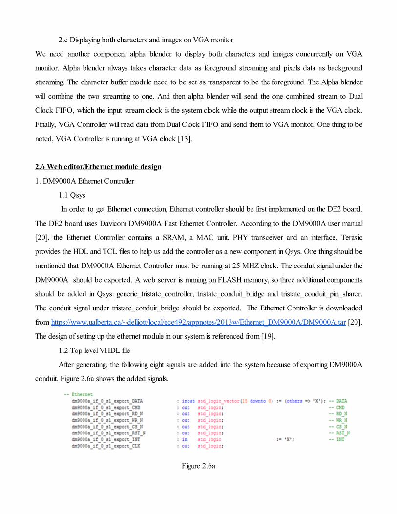
1.2 Top level VHDL file
After generating, the following eight signals are added into the system because of exporting DM9000A
conduit. Figure 2.6a shows the added signals.
Figure 2.6a
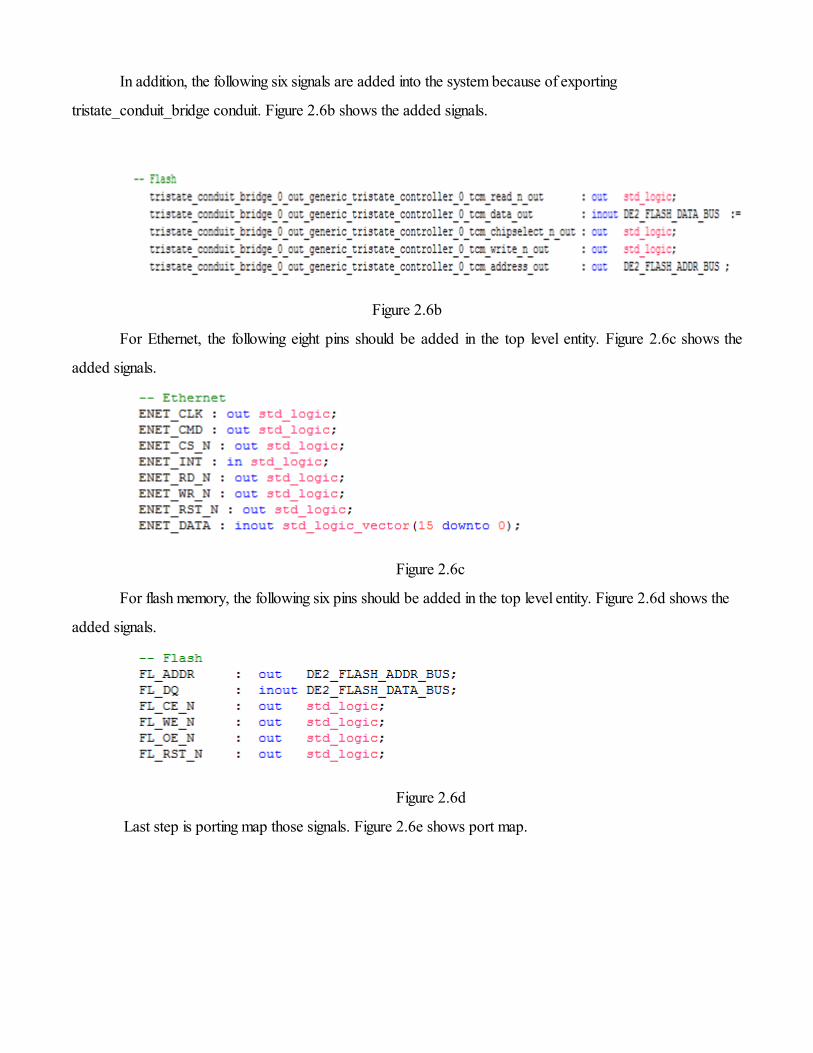
In addition, the following six signals are added into the system because of exporting
tristate_conduit_bridge conduit. Figure 2.6b shows the added signals.
Figure 2.6b
For Ethernet, the following eight pins should be added in the top level entity. Figure 2.6c shows the
added signals.
Figure 2.6c
For flash memory, the following six pins should be added in the top level entity. Figure 2.6d shows the
added signals.
Figure 2.6d
Last step is porting map those signals. Figure 2.6e shows port map.
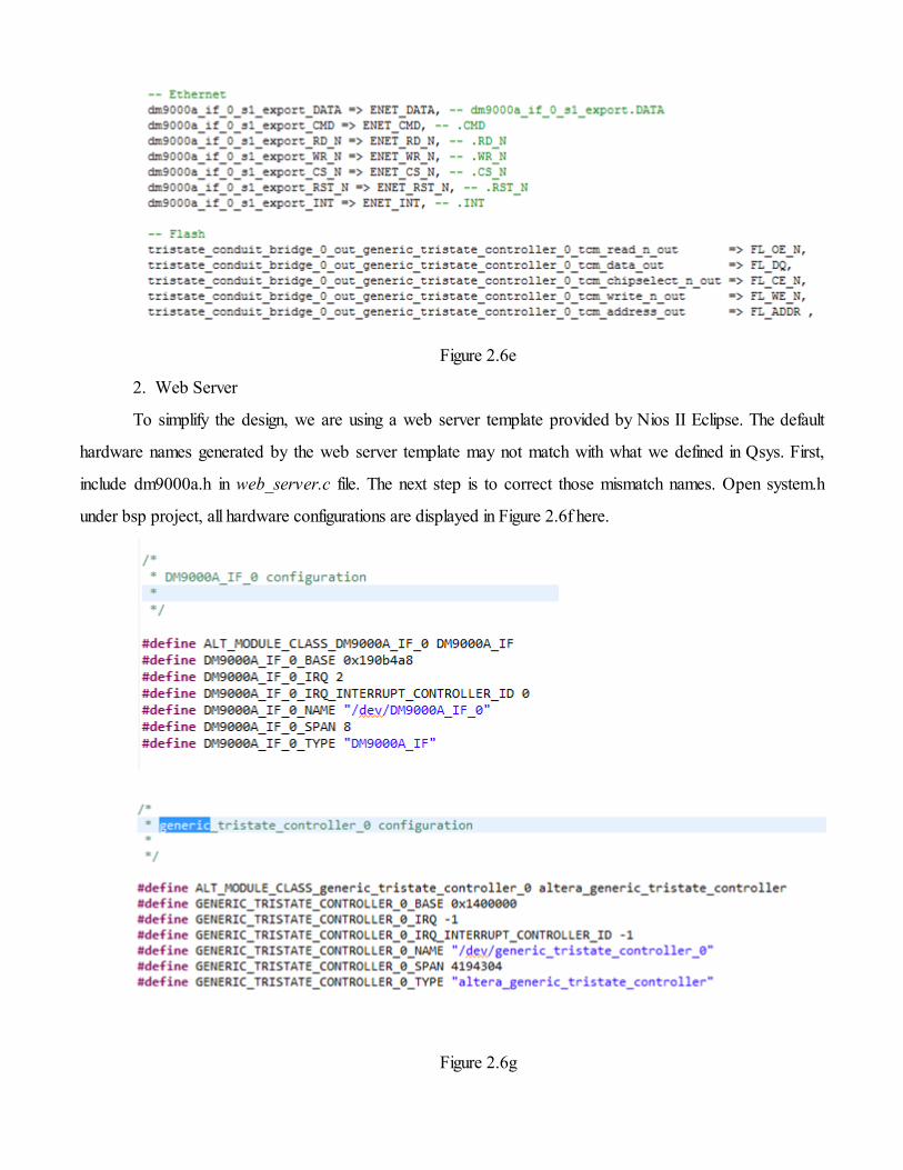
Figure 2.6e
2. Web Server
To simplify the design, we are using a web server template provided by Nios II Eclipse. The default
hardware names generated by the web server template may not match with what we defined in Qsys. First,
include dm9000a.h in web_server.c file. The next step is to correct those mismatch names. Open system.h
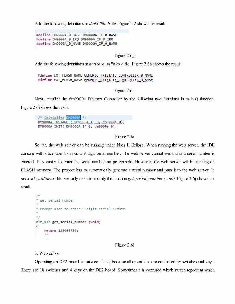
under bsp project, all hardware configurations are displayed in Figure 2.6f here.
Figure 2.6g
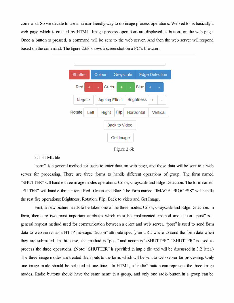
Add the following definitions in dm9000a.h file. Figure 2.2 shows the result.
Figure 2.6g
Add the following definitions in network_utilities.c file. Figure 2.6h shows the result.
Figure 2.6h
Next, initialize the dm9000a Ethernet Controller by the following two functions in main () function.
Figure 2.6i shows the result.
Figure 2.6i
So far, the web server can be running under Nios II Eclipse. When running the web server, the IDE
console will notice user to input a 9-digit serial number. The web server cannot work until a serial number is
entered. It is easier to enter the serial number on pc console. However, the web server will be running on
FLASH memory. The project has to automatically generate a serial number and pass it to the web server. In
network_utilities.c file, we only need to modify the function get_serial_number (void). Figure 2.6j shows the
result.
Figure 2.6j
3. Web editor
Operating on DE2 board is quite confused, because all operations are controlled by switches and keys.
There are 18 switches and 4 keys on the DE2 board. Sometimes it is confused which switch represent which
command. So we decide to use a human-friendly way to do image process operations. Web editor is basically a
web page which is created by HTML. Image process operations are displayed as buttons on the web page.
Once a button is pressed, a command will be sent to the web server. And then the web server will respond
based on the command. The figure 2.6k shows a screenshot on a PC’s browser.
Figure 2.6k
3.1 HTML file
“form” is a general method for users to enter data on web page, and those data will be sent to a web
server for processing. There are three forms to handle different operations of group. The form named
“SHUTTER” will handle three image modes operations: Color, Grayscale and Edge Detection. The form named
“FILTER” will handle three filters: Red, Green and Blue. The form named “IMAGE_PROCESS” will handle
the rest five operations: Brightness, Rotation, Flip, Back to video and Get Image.
First, a new picture needs to be taken one of the three modes: Color, Grayscale and Edge Detection. In
form, there are two most important attributes which must be implemented: method and action. “post” is a
general request method used for communication between a client and web server. “post” is used to send form
data to web server as a HTTP message. “action” attribute specify an URL where to send the form data when
they are submitted. In this case, the method is “post” and action is “/SHUTTER”. “SHUTTER” is used to
process the three operations. (Note: “SHUTTER” is specified in http.c file and will be discussed in 3.2 later.)
The three image modes are treated like inputs to the form, which will be sent to web server for processing. Only
one image mode should be selected at one time. In HTML, a “radio” button can represent the three image
modes. Radio buttons should have the same name in a group, and only one radio button in a group can be
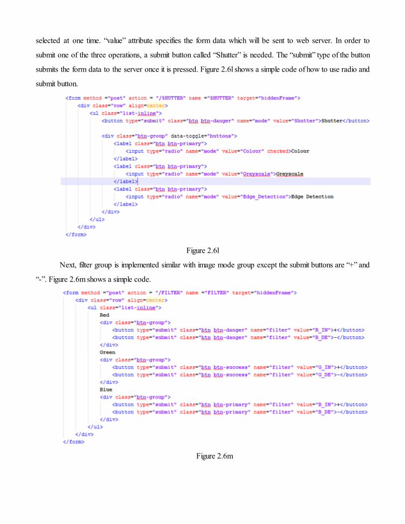
selected at one time. “value” attribute specifies the form data which will be sent to web server. In order to
submit one of the three operations, a submit button called “Shutter” is needed. The “submit” type of the button
submits the form data to the server once it is pressed. Figure 2.6l shows a simple code of how to use radio and
submit button.
Figure 2.6l
Next, filter group is implemented similar with image mode group except the submit buttons are “+” and
“-”. Figure 2.6m shows a simple code.
Figure 2.6m
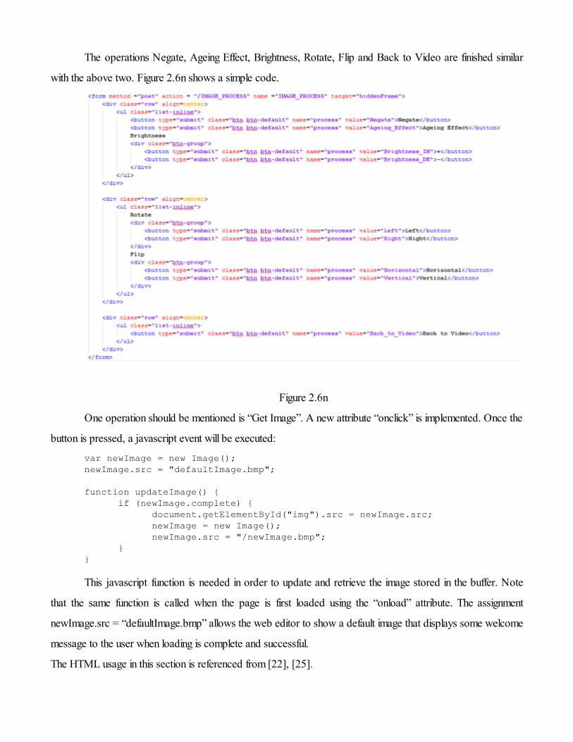
The operations Negate, Ageing Effect, Brightness, Rotate, Flip and Back to Video are finished similar
with the above two. Figure 2.6n shows a simple code.
Figure 2.6n
One operation should be mentioned is “Get Image”. A new attribute “onclick” is implemented. Once the
button is pressed, a javascript event will be executed:
var newImage = new Image(); newImage.src = "defaultImage.bmp"; function updateImage() {
if (newImage.complete) { document.getElementById("img").src = newImage.src; newImage = new Image(); newImage.src = "/newImage.bmp";
} }
This javascript function is needed in order to update and retrieve the image stored in the buffer. Note
that the same function is called when the page is first loaded using the “onload” attribute. The assignment
newImage.src = “defaultImage.bmp” allows the web editor to show a default image that displays some welcome
message to the user when loading is complete and successful.
The HTML usage in this section is referenced from [22], [25].
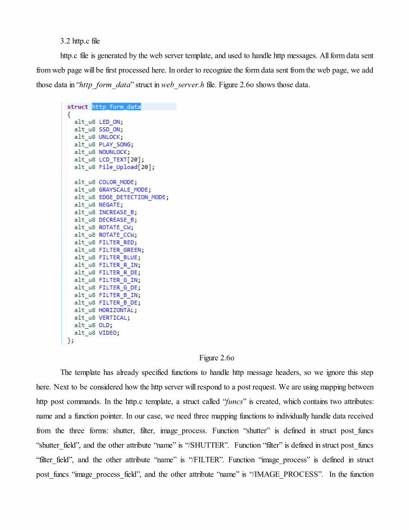
3.2 http.c file
http.c file is generated by the web server template, and used to handle http messages. All form data sent
from web page will be first processed here. In order to recognize the form data sent from the web page, we add
those data in “http_form_data” struct in web_server.h file. Figure 2.6o shows those data.
Figure 2.6o
The template has already specified functions to handle http message headers, so we ignore this step
here. Next to be considered how the http server will respond to a post request. We are using mapping between
http post commands. In the http.c template, a struct called “funcs” is created, which contains two attributes:
name and a function pointer. In our case, we need three mapping functions to individually handle data received
from the three forms: shutter, filter, image_process. Function “shutter” is defined in struct post_funcs
“shutter_field”, and the other attribute “name” is “/SHUTTER”. Function “filter” is defined in struct post_funcs
“filter_field”, and the other attribute “name” is “/FILTER”. Function “image_process” is defined in struct
post_funcs “image_process_field”, and the other attribute “name” is “/IMAGE_PROCESS”. In the function
“http_handle_post”, URI buffer sent from form will be compared with all attributes “name” in struct
post_funcs. If one gets matched, the corresponding function will be called.
The functions shutter, filter and image_process are implemented in a similar way. Here, we only explain
how function shutter is working. First, check the sent data is “Color”, “Grayscale” or “Edge_Detection”. Then,
set the corresponding attribute in http_form_data to 1. Finally, use OSMboxPost(board_control_mbox,
(void*) &board_funcs); to send a message to the specified mailbox. The web_server.c file will use (void*)
OSMboxPend(board_control_mbox, 0,&error_code); to read the message from the specified mailbox.
(web_server.c will be discussed in 3.3 later.) Figure 2.6p shows the simple code.
Figure 2.6p
3.3 web_server.c
In function “board_control_task”, the web server will first read the message to be sent to the
specified mailbox. After identifying the operation message, the web server will call corresponding functions to
process the image. Figure 2.6q shows a simple code.
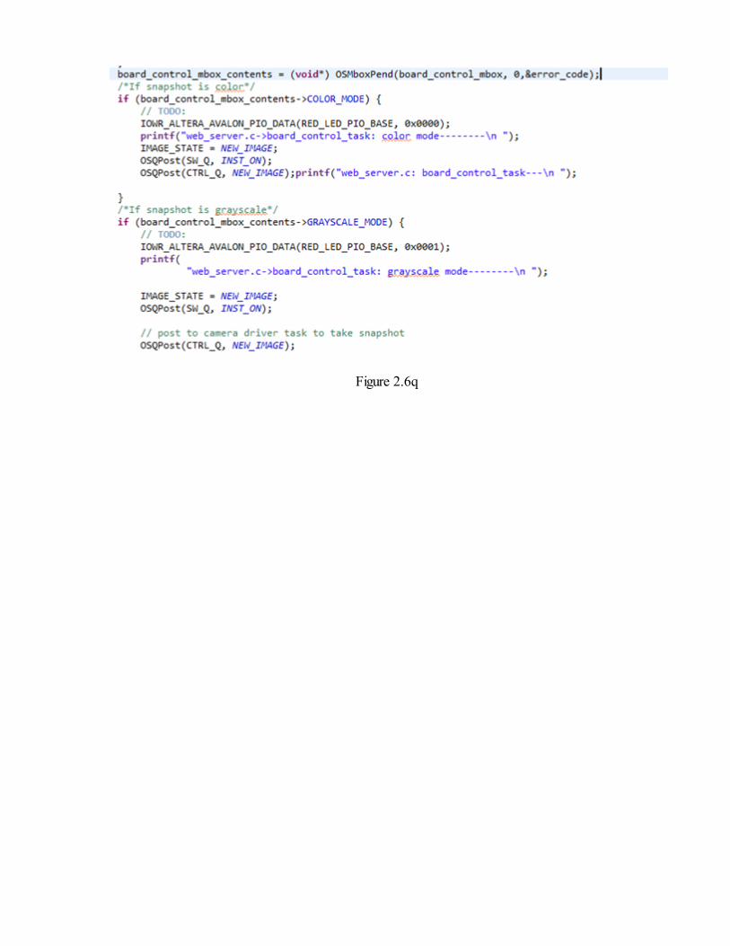
Figure 2.6q
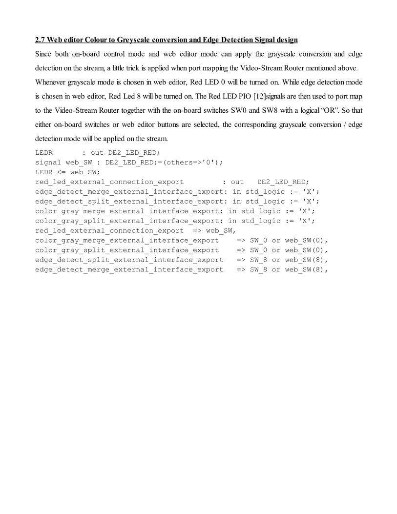
2.7 Web editor Colour to Greyscale conversion and Edge Detection Signal design
Since both on-board control mode and web editor mode can apply the grayscale conversion and edge
detection on the stream, a little trick is applied when port mapping the Video-Stream Router mentioned above.
Whenever grayscale mode is chosen in web editor, Red LED 0 will be turned on. While edge detection mode
is chosen in web editor, Red Led 8 will be turned on. The Red LED PIO [12]signals are then used to port map
to the Video-Stream Router together with the on-board switches SW0 and SW8 with a logical “OR”. So that
either on-board switches or web editor buttons are selected, the corresponding grayscale conversion / edge
detection mode will be applied on the stream.
LEDR : out DE2_LED_RED; signal web_SW : DE2_LED_RED:=(others=>'0'); LEDR <= web_SW;
red_led_external_connection_export : out DE2_LED_RED;
edge_detect_merge_external_interface_export: in std_logic := 'X';
edge_detect_split_external_interface_export: in std_logic := 'X';
color_gray_merge_external_interface_export: in std_logic := 'X';
color_gray_split_external_interface_export: in std_logic := 'X';
red_led_external_connection_export => web_SW,
color_gray_merge_external_interface_export => SW_0 or web_SW(0),
color_gray_split_external_interface_export => SW_0 or web_SW(0),
edge_detect_split_external_interface_export => SW_8 or web_SW(8),
edge_detect_merge_external_interface_export => SW_8 or web_SW(8),
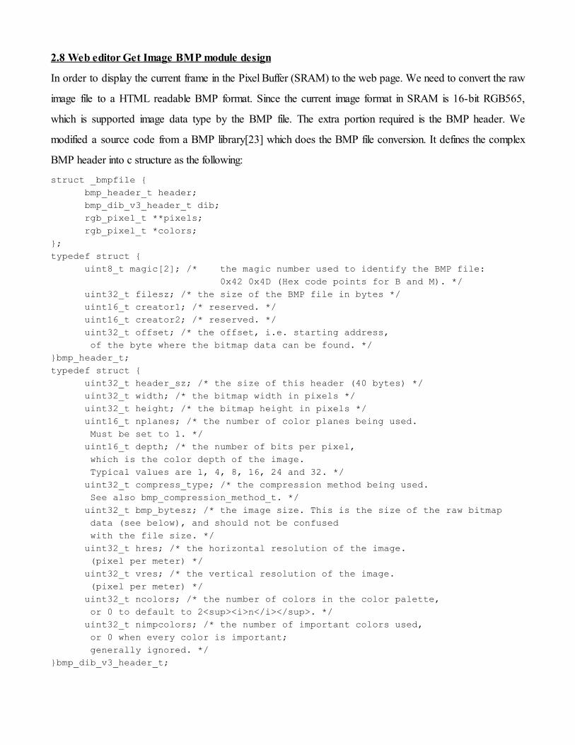
2.8 Web editor Get Image BMP module design
In order to display the current frame in the Pixel Buffer (SRAM) to the web page. We need to convert the raw
image file to a HTML readable BMP format. Since the current image format in SRAM is 16-bit RGB565,
which is supported image data type by the BMP file. The extra portion required is the BMP header. We
modified a source code from a BMP library[23] which does the BMP file conversion. It defines the complex
BMP header into c structure as the following:
struct _bmpfile {
bmp_header_t header;
bmp_dib_v3_header_t dib;
rgb_pixel_t **pixels;
rgb_pixel_t *colors;
};
typedef struct {
uint8_t magic[2]; /* the magic number used to identify the BMP file:
0x42 0x4D (Hex code points for B and M). */
uint32_t filesz; /* the size of the BMP file in bytes */
uint16_t creator1; /* reserved. */
uint16_t creator2; /* reserved. */
uint32_t offset; /* the offset, i.e. starting address,
of the byte where the bitmap data can be found. */
}bmp_header_t;
typedef struct {
uint32_t header_sz; /* the size of this header (40 bytes) */
uint32_t width; /* the bitmap width in pixels */
uint32_t height; /* the bitmap height in pixels */
uint16_t nplanes; /* the number of color planes being used.
Must be set to 1. */
uint16_t depth; /* the number of bits per pixel,
which is the color depth of the image.
Typical values are 1, 4, 8, 16, 24 and 32. */
uint32_t compress_type; /* the compression method being used.
See also bmp_compression_method_t. */
uint32_t bmp_bytesz; /* the image size. This is the size of the raw bitmap
data (see below), and should not be confused
with the file size. */
uint32_t hres; /* the horizontal resolution of the image.
(pixel per meter) */
uint32_t vres; /* the vertical resolution of the image.
(pixel per meter) */
uint32_t ncolors; /* the number of colors in the color palette,
or 0 to default to 2<sup><i>n</i></sup>. */
uint32_t nimpcolors; /* the number of important colors used,
or 0 when every color is important;
generally ignored. */
}bmp_dib_v3_header_t;
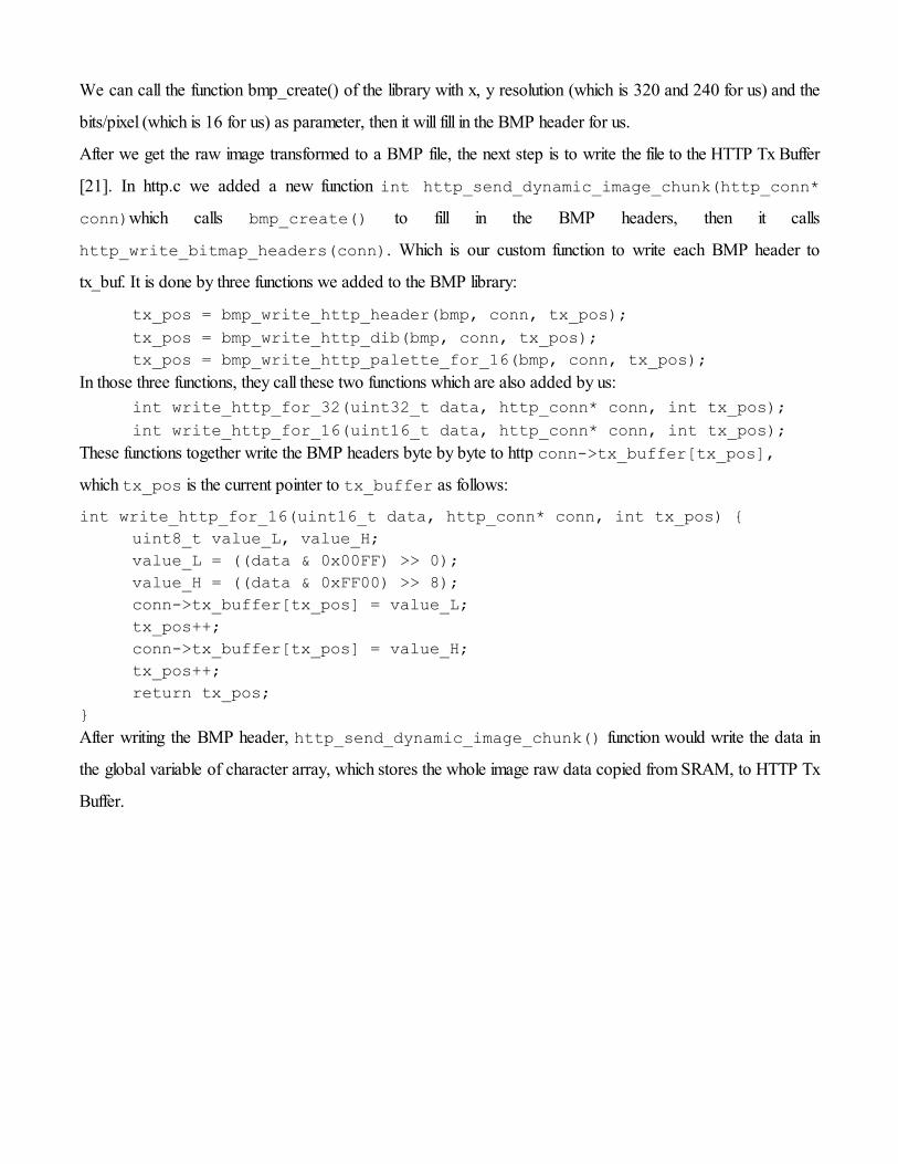
We can call the function bmp_create() of the library with x, y resolution (which is 320 and 240 for us) and the
bits/pixel (which is 16 for us) as parameter, then it will fill in the BMP header for us.
After we get the raw image transformed to a BMP file, the next step is to write the file to the HTTP Tx Buffer
[21]. In http.c we added a new function int http_send_dynamic_image_chunk(http_conn*
conn)which calls bmp_create() to fill in the BMP headers, then it calls
http_write_bitmap_headers(conn). Which is our custom function to write each BMP header to
tx_buf. It is done by three functions we added to the BMP library:
tx_pos = bmp_write_http_header(bmp, conn, tx_pos);
tx_pos = bmp_write_http_dib(bmp, conn, tx_pos);
tx_pos = bmp_write_http_palette_for_16(bmp, conn, tx_pos);
In those three functions, they call these two functions which are also added by us:
int write_http_for_32(uint32_t data, http_conn* conn, int tx_pos);
int write_http_for_16(uint16_t data, http_conn* conn, int tx_pos);
These functions together write the BMP headers byte by byte to http conn->tx_buffer[tx_pos],
which tx_pos is the current pointer to tx_buffer as follows:
int write_http_for_16(uint16_t data, http_conn* conn, int tx_pos) {
uint8_t value_L, value_H;
value_L = ((data & 0x00FF) >> 0);
value_H = ((data & 0xFF00) >> 8);
conn->tx_buffer[tx_pos] = value_L;
tx_pos++;
conn->tx_buffer[tx_pos] = value_H;
tx_pos++;
return tx_pos;
}
After writing the BMP header, http_send_dynamic_image_chunk()function would write the data in
the global variable of character array, which stores the whole image raw data copied from SRAM, to HTTP Tx
Buffer.
2.9 Image controller module design
This module was mostly software related. The image controller manages the image buffer according to messages
from other modules. It also manages the messages passed between modules. When new image option message
from user interface module was detected, image controller would allocate memory from SDRAM using calloc()
function. The size to allocate was determine by the image type selected from user interface as well. When image
operation message from user interface was detected, image controller would call the image operation functions
from image processor module to perform the operations on the image buffer. Whenever the image buffer was
updated, the controller would call the VGA module functions to display the image on the VGA screen. The
mechanism of message passing between modules in the system was build on OS Queues, which messages can
be post and pend on different modules. The messages passing around are actually numerical symbolic constants,
the advantage of using numbers to represent message is they can be added together in a message to represent
multiple meaning. For example, to represent “take a new colour image”, a message of (NEW_IMAGE +
COLOUR) can be passed; to represent “rotate a grayscale image counter clockwise”, we can pass the
message of (GRAYSCALE + ROTATE + CCW).
2.10 Image processor module design
The following modules design related to image operations and all image operation equations are original contents
developed on no more than the basic concepts of RGB formats reference from [13],[11],[14],[15].
This module provide functions that make changes on image buffer (a character array) to perform a series of
image operations. Each image operation modifies the image buffer pixel by pixel. For 8-bit grayscale operation,
every 8-bit character in the image buffer represents a pixel. So, for each operation on grayscale, apply the linear
equation of such operation on each pixel (each byte) in a loop throughout the whole buffer (represent by
buffer[i] below). For 16-bit RGB colour operation, every two character in the image buffer represents a colour
pixel. So for each colour operation, apply the linear equation of such operation on every two bytes in a loop
throughout the whole buffer (higher byte (bit 16-8) represent by buffer[i], and lower byte (bit 7-0) represent by
buffer[i+1] below).
● image invert / negate
buffer[i] = 0xFF - buffer[i]
● increase brightness on grayscale
buffer[i] = buffer[i] + BrigntnessStepSize
● decrease brightness on grayscale
buffer[i] = buffer[i] - BrigntnessStepSize
Where BrightnessStepSize was a predefined constant. Since in grayscale, 0x00 is black and 0xFF is white, to
increase brightness, just add the step size to current value so it will be closer to white. To decrease brightness,
just subtract the step size from current value so it will be closer to black.
● increase / decrease brightness on colour
It is similar to grayscale, but for colour, the addition and subtraction must be done separately on each colour
plane to prevent carries that affect other colour plane (that will change the colour). which means for each pixel,
add/subtract from its R, G and B value. So we must extract the R, G and B bits out of every two bytes before
add or subtract.
a_pixel = ((buffer[i] << 8) | (buffer[i+1] << 0))
R = ((a_pixel & 0xF800) >> 11)
G = ((a_pixel & 0x07E0) >> 5)
B = ((a_pixel & 0x001F) >> 0)
here we first group the two byte into a 16 bit pixel, then extract each colour plane by masking and shifting
correspondingly. As we known bits 15-11 is for red, bits 10-5 is for green, and bits 4-0 is for blue.
R = R + BrigntnessStepSize R = R - BrigntnessStepSize
G = G + BrigntnessStepSize G = G - BrigntnessStepSize
B = B + BrigntnessStepSize B = B - BrigntnessStepSize
After applying the set of above equations, we should put each colour plane back to the current two bytes.
a_pixel = ((R << 11) | (G << 5) | (B << 0))
buffer[i+1] = ((a_pixel & 0x00FF) >> 0)
buffer[i] = ((a_pixel & 0xFF00) >> 8)
Noted that for both colour and grayscale brightness adjustment, when we add or subtract the current pixel
value, we should make sure that the result would not exceed maximum and minimum limit. For grayscale, it
should always between 0x00 and 0xFF. For colour red and blue, it should always between 0b00000 and
0b11111 (0x00 to 0x1F). For colour green, it should always between 0b000000 and 0b111111 (0x00 to
0x3F). A range check before every add or subtract have to be done, if an add / subtract on current value will
out of range, then just set the new value to be the maximum / minimum value.
● rotations and reflections
To perform image rotation and reflections, one more temporary image buffer is needed, for each byte in the
rotated image buffer, use a linear equation to compute which is the corresponding byte from the original image
buffer. Then copy the byte from the original image buffer to the temporary image buffer. After every byte has
been copied, the temporary image buffer now stores the rotated image. At last just copy the whole temporary
buffer back to the image buffer.
Another issue need to be consider when performing rotation is that the image from the camera has a resolution
of 320x240 or 640x480. Noted the image are rectangles, when we rotate a rectangle by 90 degrees, the longer
side will become the shorter side, and vice versa. Which is very challenging to find a linear equation to perform
rotation. So, we choose to slightly adjust the image to become a square (ie: 320x320 or 640x640), by filling the
extra portion in black (0x00) for each byte. And then perform rotation on the square image. A variable that
records the current image angle was introduced for adjusting the image buffer pointer which points to the
position where the image starts in the buffer, since when displaying the image which is upside-down, we need to
skip the extra black portion that locate at the beginning of the buffer now. For details, refer to Software Design.
❏ To visualize the linear equation used on grayscale rotation, consider this example of a 3x3 grayscale
image, which its original image buffer (character / byte array) will have the following indexing:
0 1 2
3 4 5
6 7 8
● rotate 90 degrees clockwise on grayscale
Consider rotating 90 degrees clockwise on the above 3x3 example, it will becomes:
6 3 0
7 4 1
8 5 2
row = truncate (i / x)
new_index = (x * (x - (i mod x) - 1) + row)
rotated_buffer[i] = buffer[new_index]
from the above equations, i represents the index in rotated image buffer (it is loop throughout the size of the
buffer), and the result of the equation will be the corresponding index from the original image buffer. And x is the
x resolution of the image.
Applying the equation on the above 3x3 example to compute the new index when say, i = 5 (underlined above)
row = truncate (5 / 3) = 1
new_index = (3 * (3 - (5 mod 3) - 1) + row) = (3 * (3 - (2) - 1) + 1) = 1 which is the index as shown above.
● rotate 90 degrees counter clockwise on grayscale
Consider rotating 90 degrees counter clockwise on the above 3x3 example, it will becomes:
2 5 8
1 4 7
0 3 6
row = truncate (i / x)
new_index = ( (1 + (i mod x) ) * x - (1 + row) )
rotated_buffer[i] = buffer[new_index]
definitions of symbols in the equation are the same as the one for clockwise.
Applying the equation on the above 3x3 example to compute the new index when say, i = 5 (underlined above)
row = truncate (5 / 3) = 1
new_index = ( (1 + (5 mod 3) ) * 3 - (1 + row) ) = ( (1 + (2) ) * 3 - (1 + 1) ) = 7 which is the index as shown
above.
❏ To visualize the linear equation used on colour rotation, consider a similar example of a 3x3 colour
image, which its original image buffer (character / byte array) will have the following indexing, where
each pair of indexes (every 2 character / byte) represents a pixel:
(0 1) (2 3) (4 5)
(6 7) (8 9) (10 11)
(12 13) (14 15) (16 17)
● rotate 90 degrees clockwise on colour
Consider rotating 90 degrees clockwise on the above 3x3 example, it will becomes the left set of indexes:
(12 13) (6 7) (0 1) 12 6 0
(14 15) (8 9) (2 3) => 14 8 2
(16 17) (10 11) (4 5) 16 10 4
comparing this result to the 90 degrees clockwise rotation on grayscale, we can make one observation:
If we just consider the higher byte in each pixel pair, it becomes the right set of indexes above. Now look back
to the set of indexes of 90 degrees clockwise rotation on grayscale. They have this simple relation.
12 6 0 6 3 0
14 8 2 = 2 * 7 4 1
16 10 4 8 5 2
So we can conclude, to find the higher byte new index for 90 degrees clockwise rotation on colour, just divide
the temporary index by 2, apply the equation for 90 degrees clockwise rotation on grayscale, and then multiply
the result by 2. It is also obvious to find the lower byte new index now, it is just 1 plus the new index of the
higher byte.
new_index = 2 * rotate_cw_grayscale ( i / 2 )
rotated_buffer[i] = buffer[new_index]
rotated_buffer[i + 1] = buffer[new_index + 1]
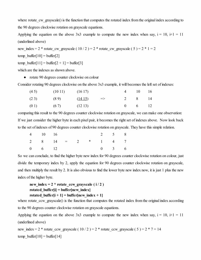
where rotate_cw_grayscale() is the function that computes the rotated index from the original index according to
the 90 degrees clockwise rotation on grayscale equations.
Applying the equation on the above 3x3 example to compute the new index when say, i = 10, i+1 = 11
(underlined above)
new_index = 2 * rotate_cw_grayscale ( 10 / 2 ) = 2 * rotate_cw_grayscale ( 5 ) = 2 * 1 = 2
temp_buffer[10] = buffer[2]
temp_buffer[11] = buffer[2 + 1] = buffer[3]
which are the indexes as shown above.
● rotate 90 degrees counter clockwise on colour
Consider rotating 90 degrees clockwise on the above 3x3 example, it will becomes the left set of indexes:
(4 5) (10 11) (16 17) 4 10 16
(2 3) (8 9) (14 15) => 2 8 14
(0 1) (6 7) (12 13) 0 6 12
comparing this result to the 90 degrees counter clockwise rotation on grayscale, we can make one observation:
If we just consider the higher byte in each pixel pair, it becomes the right set of indexes above. Now look back
to the set of indexes of 90 degrees counter clockwise rotation on grayscale. They have this simple relation.
4 10 16 2 5 8
2 8 14 = 2 * 1 4 7
0 6 12 0 3 6
So we can conclude, to find the higher byte new index for 90 degrees counter clockwise rotation on colour, just
divide the temporary index by 2, apply the equation for 90 degrees counter clockwise rotation on grayscale,
and then multiply the result by 2. It is also obvious to find the lower byte new index now, it is just 1 plus the new
index of the higher byte.
new_index = 2 * rotate_ccw_grayscale ( i / 2 )
rotated_buffer[i] = buffer[new_index]
rotated_buffer[i + 1] = buffer[new_index + 1]
where rotate_ccw_grayscale() is the function that computes the rotated index from the original index according
to the 90 degrees counter clockwise rotation on grayscale equations.
Applying the equation on the above 3x3 example to compute the new index when say, i = 10, i+1 = 11
(underlined above)
new_index = 2 * rotate_ccw_grayscale ( 10 / 2 ) = 2 * rotate_ccw_grayscale ( 5 ) = 2 * 7 = 14
temp_buffer[10] = buffer[14]
temp_buffer[11] = buffer[14 + 1] = buffer[15]
which are the indexes as shown above.
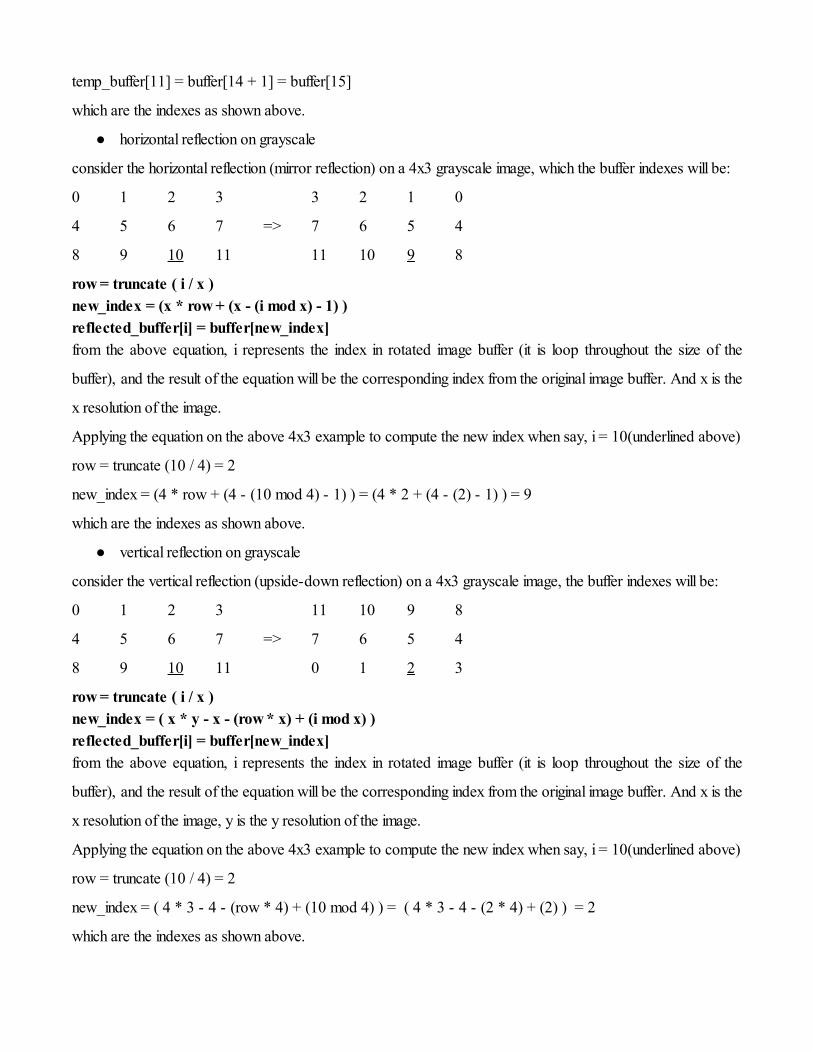
● horizontal reflection on grayscale
consider the horizontal reflection (mirror reflection) on a 4x3 grayscale image, which the buffer indexes will be:
0 1 2 3 3 2 1 0
4 5 6 7 => 7 6 5 4
8 9 10 11 11 10 9 8
row = truncate ( i / x )
new_index = (x * row + (x - (i mod x) - 1) )
reflected_buffer[i] = buffer[new_index]
from the above equation, i represents the index in rotated image buffer (it is loop throughout the size of the
buffer), and the result of the equation will be the corresponding index from the original image buffer. And x is the
x resolution of the image.
Applying the equation on the above 4x3 example to compute the new index when say, i = 10(underlined above)
row = truncate (10 / 4) = 2
new_index = (4 * row + (4 - (10 mod 4) - 1) ) = (4 * 2 + (4 - (2) - 1) ) = 9
which are the indexes as shown above.
● vertical reflection on grayscale
consider the vertical reflection (upside-down reflection) on a 4x3 grayscale image, the buffer indexes will be:
0 1 2 3 11 10 9 8
4 5 6 7 => 7 6 5 4
8 9 10 11 0 1 2 3
row = truncate ( i / x )
new_index = ( x * y - x - (row * x) + (i mod x) )
reflected_buffer[i] = buffer[new_index]
from the above equation, i represents the index in rotated image buffer (it is loop throughout the size of the
buffer), and the result of the equation will be the corresponding index from the original image buffer. And x is the
x resolution of the image, y is the y resolution of the image.
Applying the equation on the above 4x3 example to compute the new index when say, i = 10(underlined above)
row = truncate (10 / 4) = 2
new_index = ( 4 * 3 - 4 - (row * 4) + (10 mod 4) ) = ( 4 * 3 - 4 - (2 * 4) + (2) ) = 2
which are the indexes as shown above.
● horizontal reflection on colour
For the similar observations and reasons of colour rotation, we can apply grayscale horizontal reflection
functions with additional calculations to obtain the new index for horizontal reflection on colour.
new_index = 2 * reflect_horizontal_grayscale ( i / 2 )
reflected_buffer[i] = buffer[new_index]
reflected_buffer[i + 1] = buffer[new_index + 1]
where reflect_horizontal_grayscale() is the function that computes the reflected index from the original index
according to the horizontal reflection on grayscale equations.
● vertical reflection on colour
For the similar observations and reasons of colour rotation, we can apply grayscale vertical reflection functions
with additional calculations to obtain the new index for vertical reflection on colour.
new_index = 2 * reflect_vertical_grayscale ( i / 2 )
reflected_buffer[i] = buffer[new_index]
reflected_buffer[i + 1] = buffer[new_index + 1]
where reflect_vertical_grayscale() is the function that computes the reflected index from the original index
according to the vertical reflection on grayscale equations.
● colour filters
Colour filters implementations are very similar to brightness adjustment, just apply addition or subtraction on the
Red, Green or Blue bits in the pixel according to user input with a different step size.
R = R + FilterStepSize R = R - FilterStepSize
G = G + FilterStepSize G = G - FilterStepSize
B = B + FilterStepSize B = B FilterStepSize
● ageing effect
Ageing effect is a special case of colour filter, which applies the following functions
R = R + 0x3
G = G + 0x2
B = B - 0x3
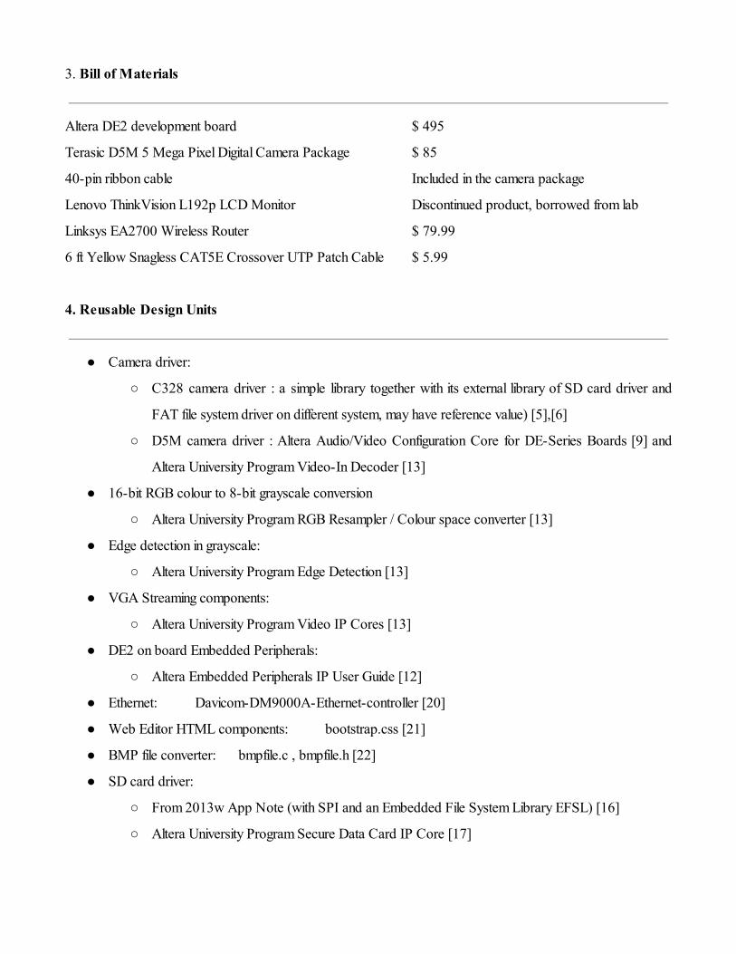
3. Bill of Materials
Altera DE2 development board $ 495
Terasic D5M 5 Mega Pixel Digital Camera Package $ 85
40-pin ribbon cable Included in the camera package
Lenovo ThinkVision L192p LCD Monitor Discontinued product, borrowed from lab
Linksys EA2700 Wireless Router $ 79.99
6 ft Yellow Snagless CAT5E Crossover UTP Patch Cable $ 5.99
4. Reusable Design Units
● Camera driver:
○ C328 camera driver : a simple library together with its external library of SD card driver and
FAT file system driver on different system, may have reference value) [5],[6]
○ D5M camera driver : Altera Audio/Video Configuration Core for DE-Series Boards [9] and
Altera University Program Video-In Decoder [13]
● 16-bit RGB colour to 8-bit grayscale conversion
○ Altera University Program RGB Resampler / Colour space converter [13]
● Edge detection in grayscale:
○ Altera University Program Edge Detection [13]
● VGA Streaming components:
○ Altera University Program Video IP Cores [13]
● DE2 on board Embedded Peripherals:
○ Altera Embedded Peripherals IP User Guide [12]
● Ethernet: Davicom-DM9000A-Ethernet-controller [20]
● Web Editor HTML components: bootstrap.css [21]
● BMP file converter: bmpfile.c , bmpfile.h [22]
● SD card driver:
○ From 2013w App Note (with SPI and an Embedded File System Library EFSL) [16]
○ Altera University Program Secure Data Card IP Core [17]
5. Datasheet
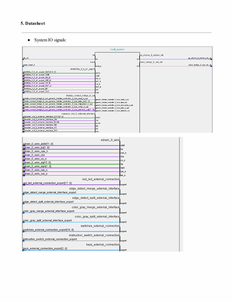
● System IO signals:
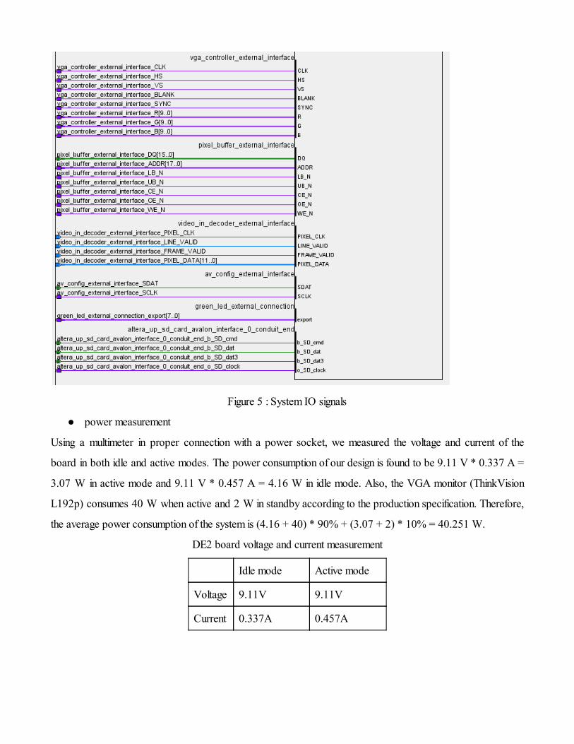
Figure 5 : System IO signals
● power measurement
Using a multimeter in proper connection with a power socket, we measured the voltage and current of the
board in both idle and active modes. The power consumption of our design is found to be 9.11 V * 0.337 A =
3.07 W in active mode and 9.11 V * 0.457 A = 4.16 W in idle mode. Also, the VGA monitor (ThinkVision
L192p) consumes 40 W when active and 2 W in standby according to the production specification. Therefore,
the average power consumption of the system is (4.16 + 40) * 90% + (3.07 + 2) * 10% = 40.251 W.
DE2 board voltage and current measurement
Idle mode Active mode
Voltage 9.11V 9.11V
Current 0.337A 0.457A
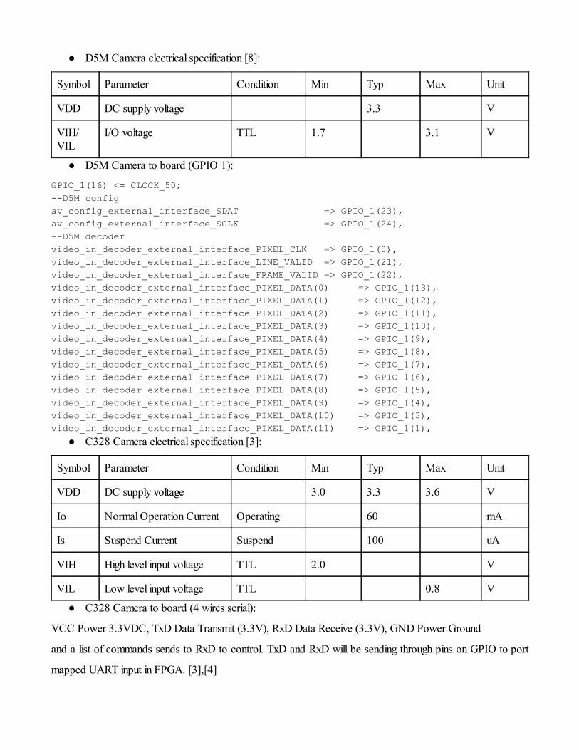
● D5M Camera electrical specification [8]:
Symbol Parameter Condition Min Typ Max Unit
VDD DC supply voltage 3.3 V
VIH/ VIL
I/O voltage TTL 1.7 3.1 V
● D5M Camera to board (GPIO 1):
GPIO_1(16) <= CLOCK_50;
--D5M config
av_config_external_interface_SDAT => GPIO_1(23),
av_config_external_interface_SCLK => GPIO_1(24),
--D5M decoder
video_in_decoder_external_interface_PIXEL_CLK => GPIO_1(0),
video_in_decoder_external_interface_LINE_VALID => GPIO_1(21),
video_in_decoder_external_interface_FRAME_VALID=> GPIO_1(22),
video_in_decoder_external_interface_PIXEL_DATA(0) => GPIO_1(13),
video_in_decoder_external_interface_PIXEL_DATA(1) => GPIO_1(12),
video_in_decoder_external_interface_PIXEL_DATA(2) => GPIO_1(11),
video_in_decoder_external_interface_PIXEL_DATA(3) => GPIO_1(10),
video_in_decoder_external_interface_PIXEL_DATA(4) => GPIO_1(9),
video_in_decoder_external_interface_PIXEL_DATA(5) => GPIO_1(8),
video_in_decoder_external_interface_PIXEL_DATA(6) => GPIO_1(7),
video_in_decoder_external_interface_PIXEL_DATA(7) => GPIO_1(6),
video_in_decoder_external_interface_PIXEL_DATA(8) => GPIO_1(5),
video_in_decoder_external_interface_PIXEL_DATA(9) => GPIO_1(4),
video_in_decoder_external_interface_PIXEL_DATA(10) => GPIO_1(3),
video_in_decoder_external_interface_PIXEL_DATA(11) => GPIO_1(1), ● C328 Camera electrical specification [3]:
Symbol Parameter Condition Min Typ Max Unit
VDD DC supply voltage 3.0 3.3 3.6 V
Io Normal Operation Current Operating 60 mA
Is Suspend Current Suspend 100 uA
VIH High level input voltage TTL 2.0 V
VIL Low level input voltage TTL 0.8 V
● C328 Camera to board (4 wires serial):
VCC Power 3.3VDC, TxD Data Transmit (3.3V), RxD Data Receive (3.3V), GND Power Ground
and a list of commands sends to RxD to control. TxD and RxD will be sending through pins on GPIO to port
mapped UART input in FPGA. [3],[4]
6. Background Reading
In the article “colour Image to Grayscale Image Conversion” [15] and the altera document “Video IP
Cores for Altera DE Series Boards, chapter 3.3” [13], it explained in every pixel, colours of an image are
represented with red, green and blue. Depending on different requirement, colours can be save in low, medium
and high quality, which is that low colour image is saved in 8 bit, medium colour image is saved in 16 bit and
high colour image is saved in 32 bit. In our design, the image buffer in SRAM stores a RBG565 format image.
The RBC565 format image is represented in 16 bit. Bit position (0-4) is represented blue value, bit position
(5-10) is represented green value and bit position (11-15) is represented red value. Base on this idea, we can
process images by changing different bits in a pixel.
From the article “Spectral colour image processing” [14], we learned about different kinds of image
processing operations, such as Spectral negation [1-S(λi )], Illumination variation: Spectrum intensity
increment/decrement, Spectral Negation with maximum value max [S(λi )]− S(λ i ). We develop our ideas of
digital image operations based on this article.
From the appnote “DM9000A Ethernet Controller”[19], we learned how to implement hardware and
software configurations of a DM9000A Ethernet Controller on DE2 board. For hardware configuration, after
adding the DM9000A Ethernet Controller as a new component on Qsys, we needed to
modify the top level VHDL file to connect the controller. For example, connect to right clock, necessary signals
and pins. For software configuration, the NIOS IDE will generate a web server template for users. We needed
to correct default hardware names to match with the hardware names which were defined in Qsys by us.
Moreover, the controller should be initialized by the following two functions defined in DM9000A.h:
DM9000A_INSTANCE() and DM9000A_INIT().
We implemented SD Card Interfacing by the help of appnote “SD Card Interfacing”[16]. First, the
appnote specifically explained how to interface with a SD card by adding the Altera University Program SD
Card Interface and modifying top level vhdl file. Then, the appnote gave an sample code to show how to
initialize the device. All reading and writing activities related to the SD card are based on the initialization step.
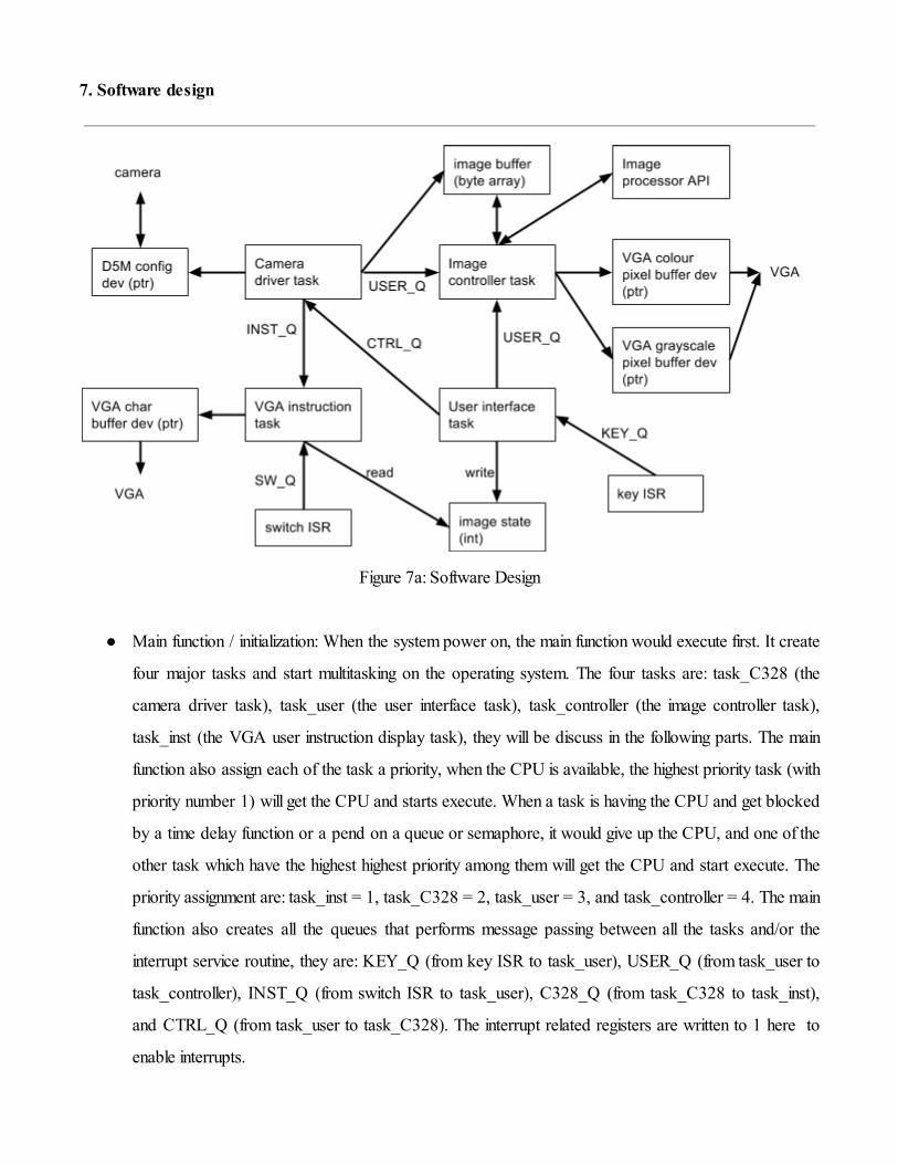
7. Software design
Figure 7a: Software Design
● Main function / initialization: When the system power on, the main function would execute first. It create
four major tasks and start multitasking on the operating system. The four tasks are: task_C328 (the
camera driver task), task_user (the user interface task), task_controller (the image controller task),
task_inst (the VGA user instruction display task), they will be discuss in the following parts. The main
function also assign each of the task a priority, when the CPU is available, the highest priority task (with
priority number 1) will get the CPU and starts execute. When a task is having the CPU and get blocked
by a time delay function or a pend on a queue or semaphore, it would give up the CPU, and one of the
other task which have the highest highest priority among them will get the CPU and start execute. The
priority assignment are: task_inst = 1, task_C328 = 2, task_user = 3, and task_controller = 4. The main
function also creates all the queues that performs message passing between all the tasks and/or the
interrupt service routine, they are: KEY_Q (from key ISR to task_user), USER_Q (from task_user to
task_controller), INST_Q (from switch ISR to task_user), C328_Q (from task_C328 to task_inst),
and CTRL_Q (from task_user to task_C328). The interrupt related registers are written to 1 here to
enable interrupts.
● User Interface: Pend on messages from ImageState queue (post by Image Controller) to control VGA,
PIO keys and PIO switches.
○ VGA: a task that display every user options on switches and keys on current image state..
○ PIO keys: keys are interrupt base PIO. A key used to send a “take a picture” signal to the
Camera driver, a key used to send a “refresh” signal to Image controller, and a key used to
send a “save to SD card” message to Image controller as well. From a key ISR, handle the
interrupt generated by the PIO key when it is pressed, post a message through a Key queue.
○ PIO switches: according to operation design, each switch is assigned to represent a user option
of image operation. A function is used to perform switch option validation when “refresh” key is
pressed (ie: queue message returns for that key). One of the switch is using the interrupt
functionality to perform runtime on/off for the user instruction display on VGA screen.
● Camera command API for C328 camera: The camera C328 operates by sending and receiving
commands of 6 byte long, each byte contains a parameter. Every command starts with a prefix of first
two bytes are always 0xAA. Major commands are SYNC, ACK, Initial, SnapShot, GetPicture, Data,
PowerOff.
○ This camera command API provides a wrapper of the parameters that forms every camera
command that are useful.
○ This API can receive bytes one by one from UART task, reform the command from every 6
bytes. Forward the command to Camera driver. Also inform Camera driver (via queue
message) when current 6 bytes cannot form a valid command.
● UART for C328 camera: Used to communicate between Camera driver and the camera.
○ From a UART ISR, handle the interrupt generated by the UART, identify what cause the
interrupt (mainly transmit ready, receive ready, and errors/exception) , post the corresponding
message to the UART queue.
○ From the UART task, pend on the messages from the UART queue, if it is receive ready, it
means a byte from camera is in Rx, check if it is a camera command (when first 0xAA receive,
0xAA together with next 5 bytes form a command), send the 6 bytes to Camera command
API.
○ When message from queue is transmit ready, it means Tx is ready for next byte, get the next
byte to be sent from Camera driver, write it to Tx.
○ When message from queue is any error/exception, inform the Camera driver via queue.
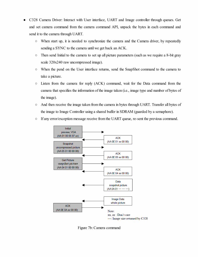
● C328 Camera Driver: Interact with User interface, UART and Image controller through queues. Get
and set camera command from the camera command API, unpack the bytes in each command and
send it to the camera through UART.
○ When start up, it is needed to synchronize the camera and the Camera driver, by repeatedly
sending a SYNC to the camera until we get back an ACK.
○ Then send Initial to the camera to set up all picture parameters (such as we require a 8-bit gray
scale 320x240 raw uncompressed image).
○ When the pend on the User interface returns, send the SnapShot command to the camera to
take a picture.
○ Listen from the camera for reply (ACK) command, wait for the Data command from the
camera that specifies the information of the image taken (i.e., image type and number of bytes of
the image).
○ And then receive the image taken from the camera in bytes through UART. Transfer all bytes of
the image to Image Controller using a shared buffer in SDRAM (guarded by a semaphore).
○ If any error/exception message receive from the UART queue, re-sent the previous command.
Figure 7b: Camera command
● Image controller API: Manage the memory buffers (using semaphores) in SDRAM which stores the
image under process. Uncompressed image from the Camera driver is stored in a global character
(same as byte / 8-bit binary) array data structure, which is in software heap (we configure software
heap to use SDRAM). And the image stored in the buffer is guarded by a semaphore. Interact with
Image processor, Camera driver, SD card and VGA.
○ Keep track of the state of current image in SDRAM (such as grayscale or colour, which
operations had been applied). Based on current state, inform User interface (via queue).
○ Pend on the shared buffer in SDRAM which contains the raw image bytes, when it is ready
from the Camera driver, signals VGA to display the image.
○ When “refresh” message from User interface is received, signal the Image processor to do
image operations. Pend on the buffer which stores the processed image, when it is ready, signals
VGA to display the new image.
○ When “save to SD card” message from User interface is received, write the image buffer (ie. the
character array) to a FILE data structure, and signal SD card controller.
○ The angle variable: records the current image angle for display purpose. where NORMAL = 0
which is the original position. Special angles for clockwise are 90, 180, 360. Special angles for
counter clockwise are -90, -180, -360. Whenever image rotate clockwise, angle + 90.
Whenever image rotate counter clockwise, angle - 90. Whenever image is reflected vertically,
angle needed to be update as well. Whenever angle equals -360 or 360, angle reset to
NORMAL. When angle equals 180 or -180, need to adjust the image buffer pointer which
points to the position where the image starts in the buffer.
● Image processor: When pend on “refresh” from User interface and pend on global image buffer both
returns, perform image operations (when hardware accelerator implemented, also interface with it).
○ Grayscale invert: since each byte represents a pixel in grayscale, for each byte in the image
buffer, update its value by subtracting it from 0xFF.
○ Colour negate: similar to grayscale invert, for each byte in the image FILE, update its value by
subtracting it from 0xFFFF.
○ Colour to greyscale: interface with the module of RGB Resampler or Colour space converter
which is the build in hardware in Altera Video IP core that can do the 16-bit RGB colour to
8-bit grayscale conversion.
○ Edge detection: interface with the module of Edge detection which is the build in hardware in
Altera Video IP core that can perform edge detection in grayscale.
○ Adjust brightness: for grayscale, 0x00 is black and 0xFF is white. For colour, 0x0000 is black
and 0xFFFF is white. To change the brightness, we define a step size for grayscale and a
different step size for colour. Loop for every byte in the image buffer, to increase brightness, just
add the current value in each byte by the step size. To decrease the brightness, just subtract the
current value in each byte by the step size. If the result of add or subtract is out of bound (i.e.,
less than 0 or larger than F) then set it to the boundary value (i.e., 0 or F).
○ Rotation: details are mentioned in Design and Operation description.
○ Reflection: details are mentioned in Design and Operation description.
○ When an image operation is done, post to a queue to inform Image controller.
● Output interface: pend on the queues posted by the Image controller and User interface.
○ SD card controller: when “save to SD card” message from User interface returned and pend on
global image buffer also returns. Interface with SD card controller to write the image to SD
card.
○ VGA controller: when “image updated” message from Image controller returned and pend on
global image buffer also returns. Interface with VGA controller to display the new image.
● Web editor task:
○ refer to Design and Description of Operation
8. Test Plan
Unit tests on hardware:
● To test the PIO KEY: send the interrupt signal from the PIO KEY to LCD to display a message. If it
display correctly, the signal is good.
● To test the camera: send and receive the basic camera manufacturer specified commands (through
Altera University Program Video Config core) to take the snapshot picture from the camera, send it
back through GPIO. Then directly sends the bytes of the image out from the VGA port (or through any
other easier possible port) on DE2 to the lab machine (or a VGA screen). Save and open the captured
image on the screen to check if a correct and complete image can be display.
● To test the UART core: port map the UART output to RS232 serial port on the board, connect the
output to lab machine, and run a test program on lab machine which displays characters send to/read
from the UART on board. From the side of on board UART, characters send to/read from the test
program on lab machine can be display using printf functions added in software. If both sides can
display characters as expected, UART core is correctly functioned.
○ The program for serial I/O: http://www.compuphase.com/software_termite.htm
Unit tests on software:
● To test the User interface: Test of each user option input (switches and keys) are detected by displaying
messages with test program printf. Also test the flow control of the user interface to check if every
display and internal image state change is correct. User options validation needed to be tested here as
well.
● To test the image quality: once the camera is tested, the procedure of testing the camera can be
repeated using different parameters in the camera commands until we get a good enough image.
● To test the image operations: Assume we have the input image with correct format stored in SRAM, by
generating some template image file in software. Run the test program which performs the image
operations, sends the bytes of the image out from the VGA port (or through any other easier possible
port) on DE2 to the lab machine (or a VGA screen). Save and open the captured image on the screen
to check if a correct and complete image after the operation can be display.
Integration tests:
● combine all the software components and hardware components, and apply processing operations on
the real images.
Acceptance tests:
● To test the processing speed of each image operation using on-board control mode.
● To test the processing speed of each image operation using web editor control mode.
● To test the speed of loading the image in SRAM to the web page.
9. Results of Experiments and Characterization
9.1 Simulation Result of Ageing Effect Algorithm
In order to determine the feasibility of the project, as well as to estimate the performance, a simulation is done
using the Matlab environment. A Matlab function is created to model one of the functions of the project.
function [ pic_old ] = oldEffect( in_pic ) % This function adds an aging effect to the input image. % The function is used as a simulation for the real project, and therefore % certain codes are inserted as means of measuring the performance of the % algorithm. % Author: Xiang Gao % Algorithm idea produced from scratch % Display the memory usage at the beginning of the function execution, and % start a stopwatch to measure the time elapsed during the execution memory tic; % Read the input image file pic=imread(in_pic); % Find the dimension of the input image [height,width,rgb]=size(pic); pixel=height*width*rgb; red=1; green=2; blue=3; % Create an empty 3D matrix for storing output image pic_old=zeros(height,width,rgb,'uint8'); % Nested loop that changes the colour information of each pixel for i=1:rgb for j=1:width for k=1:height if i==red % Add more red to the image if (pic(k,j,i)+20)>255 pic_old(k,j,i)=255; else pic_old(k,j,i)=pic(k,j,i)+20; end elseif i==green
% Add more green to the image if (pic(k,j,i)+15)>255 pic_old(k,j,i)=255; else pic_old(k,j,i)=pic(k,j,i)+15; end elseif i==blue % Remove some blue from the image if (pic(k,j,i)-20)<0 pic_old(k,j,i)=0; else pic_old(k,j,i)=pic(k,j,i)-20; end end end end end % Display the memory usage of MATLAB after the execution, stop the % stopwatch and show the time elapsed memory whos execution_time=toc; str_time=['Execution time is ',num2str(execution_time),' sec']; disp(str_time); % Display the images alongside each other subplot(1,2,1); imshow(pic); title('Original Image'); subplot(1,2,2); imshow(pic_old); title('Old Effect Image'); end
To execute the function, first define the input variable. For example: i='test.jpg'. Note that the single
quotation marks cannot be missed. Next, call the function with i as the input argument: oldEffect(i). The
following messages were printed out by the function.
Memory usage at the beginning of the execution: The following result is randomly picked from one of the executions. Maximum possible array: 13451 MB (1.410e+10 bytes) * Memory available for all arrays: 13451 MB (1.410e+10 bytes) * Memory used by MATLAB: 739 MB (7.750e+08 bytes) Physical Memory (RAM): 8080 MB (8.472e+09 bytes) * Limited by System Memory (physical + swap file) available. Memory usage at the end of the execution: Maximum possible array: 13450 MB (1.410e+10 bytes) * Memory available for all arrays: 13450 MB (1.410e+10 bytes) * Memory used by MATLAB: 740 MB (7.760e+08 bytes) Physical Memory (RAM): 8080 MB (8.472e+09 bytes)
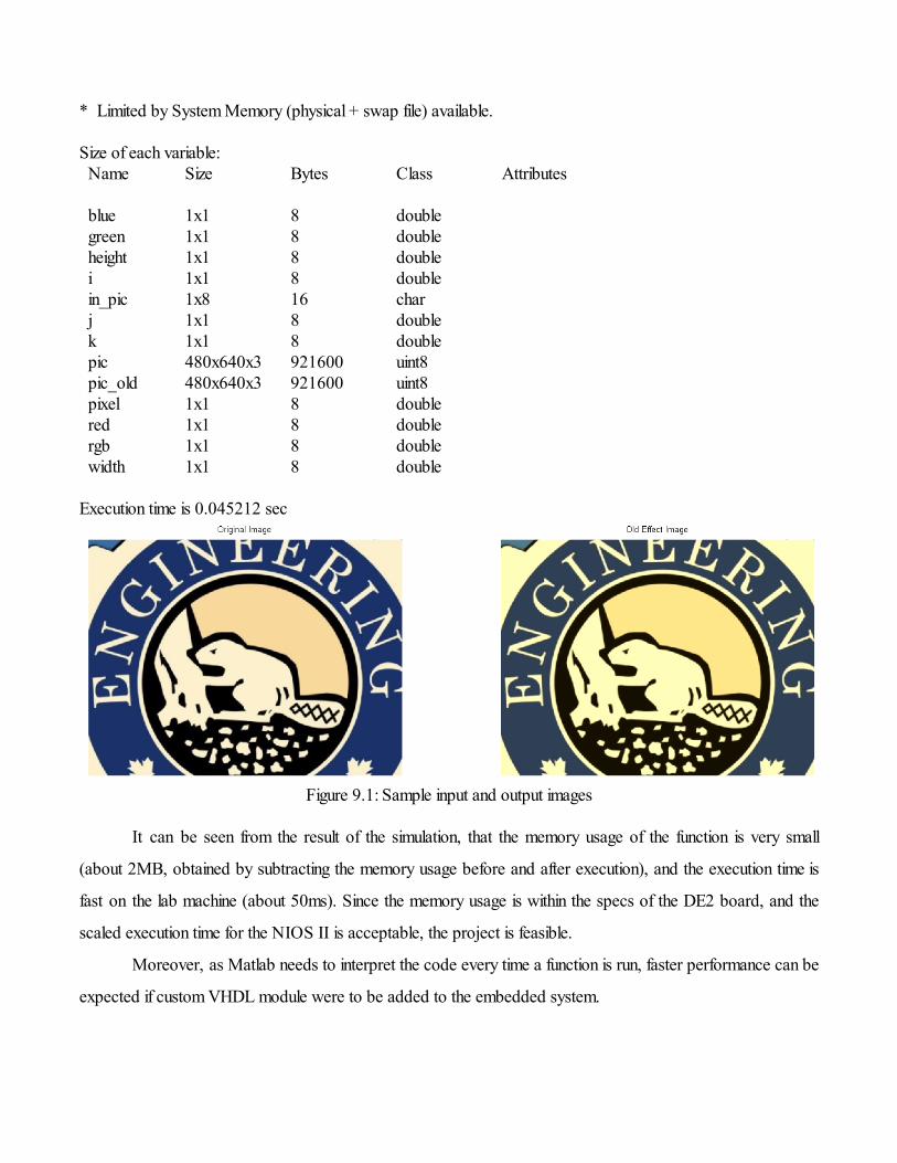
* Limited by System Memory (physical + swap file) available. Size of each variable: Name Size Bytes Class Attributes blue 1x1 8 double green 1x1 8 double height 1x1 8 double i 1x1 8 double in_pic 1x8 16 char j 1x1 8 double k 1x1 8 double pic 480x640x3 921600 uint8 pic_old 480x640x3 921600 uint8 pixel 1x1 8 double red 1x1 8 double rgb 1x1 8 double width 1x1 8 double Execution time is 0.045212 sec
Figure 9.1: Sample input and output images
It can be seen from the result of the simulation, that the memory usage of the function is very small
(about 2MB, obtained by subtracting the memory usage before and after execution), and the execution time is
fast on the lab machine (about 50ms). Since the memory usage is within the specs of the DE2 board, and the
scaled execution time for the NIOS II is acceptable, the project is feasible.
Moreover, as Matlab needs to interpret the code every time a function is run, faster performance can be
expected if custom VHDL module were to be added to the embedded system.
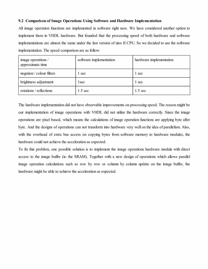
9.2 Comparison of Image Operations Using Software and Hardware Implementation
All image operation functions are implemented in software right now. We have considered another option to
implement them in VHDL hardware. But founded that the processing speed of both hardware and software
implementations are almost the same under the fast version of nios II CPU. So we decided to use the software
implementation. The speed comparison are as follow:
image operations / approximate time
software implementation hardware implementation
negation / colour filters 1 sec 1 sec
brightness adjustment 1sec 1 sec
rotations / reflections 1.5 sec 1.5 sec
The hardware implementation did not have observable improvements on processing speed. The reason might be
our implementation of image operations with VHDL did not utilize the hardware correctly. Since the image
operations are pixel based, which means the calculations of image operation functions are applying byte after
byte. And the designs of operations can not transform into hardware very well on the idea of parallelism. Also,
with the overhead of extra bus access on copying bytes from software memory to hardware modules, the
hardware could not achieve the acceleration as expected.
To fix this problem, one possible solution is to implement the image operations hardware module with direct
access to the image buffer (ie: the SRAM). Together with a new design of operations which allows parallel
image operation calculations such as row by row or column by column update on the image buffer, the
hardware might be able to achieve the acceleration as expected.

9.3 Comparison of C328 camera and D5M camera
We have tried to use the C328 camera and D5M camera in the project. C328 camera uses an UART interface
to communicate with our system, it involves sending and receiving camera specific commands in series of bytes
via UART to control the camera, we were successful to build a driver using those commands to use the C328
camera. But the images we get back through the UART were corrupted, the reason was there are too many
internal technical timing issues on the C328 camera, and that cause a data overrun on the receive buffer in the
UART. We had observed about 0.3% to 5% loss of data bytes when getting the whole image from the C328
camera, as a result of byte loss and data shift, the colour and position of the pixels on the image was not copied
to the image buffer in SRAM in a right way, and we can not get a correct image from the C328 camera. We
had tried to solve the problem by raising the CPU processing speed to catch up with the delay that cause data
overrun, and also using a different UART with larger internal FIFO buffer. However, neither of the two
approaches could solve the problem completely.
The other option is the Terasic D5M camera, it works well for our system. The D5M camera has a GPIO
interface which can directly output the image data to SRAM on the DE2 board using the system bus, and it also
has a well designed driver and video decoder from the Altera University Program. So we decided to use the
D5M camera for our system.
10. Safety
1. In our project, the main external devices are a D5M Camera and an SD card. No restricted or
dangerous material will be used in our project.
2. The voltage level compatible with DE2 is 0-3.3v. The selected camera must meet this requirement. On
the user manual of our selected D5M Camera shows that the camera satisfies the requirement, which
supports 3.3v power and 1.7-3.1v I/O. Details of maximum and average power will be discussed in
Sustainability section.
3. To safely handle the DE2 board and other electronics, an Anti Static Wrist Strap is worn at anytime.
4. No high voltage electronics is required.
11. Environmental Impact
The hardware we are using in this project includes one Altera DE2 board, Lenovo ThinkVision L192p VGA
monitor, Terasic D5M Digital Camera, and a Linksys EA2700 Wireless Router. The major raw materials
consumed in EP manufacture are elements of Halogen family and metals, like Pb, Cu, Au, Hg, Cd and Cr. The
production of process will release toxic gas and sewage, which will have unrecoverable severe impacts on
human and environment. The emissions of those hazardous substances will cause land barren and human will get
infected with disease if accumulate too high volume heavy metal. Moreover, the emission of chlorine dioxide gas
will lead ozone depletion.
In order to protect our environment and human health, using lead-free solders in electrical products is
promoted. As an alternative, SnAgCu is preferred to reduce environmental impact.
On Altera web site, it announced “Altera offers device packages that are fully compliant with the
restriction of hazardous substances (RoHS) directive adopted by the European Union”. (
http://www.altera.com/support/reliability/environmental/lead-free/rel-lead-free.html). The ThinkVision VGA
monitor is advertised compliant with RoHS on the lenovo web site.
(http://support.lenovo.com/fr_MA/product-and-parts/detail.page?DocID=PD027465.html). The Terasic D5M
Digital Camera is RoHS compliant according to the product’s ordering page
(http://www.terasic.com.tw/cgi-bin/page/archive.pl?Language=English&CategoryNo=68&No=281&PartNo=5
). The Linksys EA2700 Wireless Router also satisfies RoHS compliance according to the user manual that
come with the package.
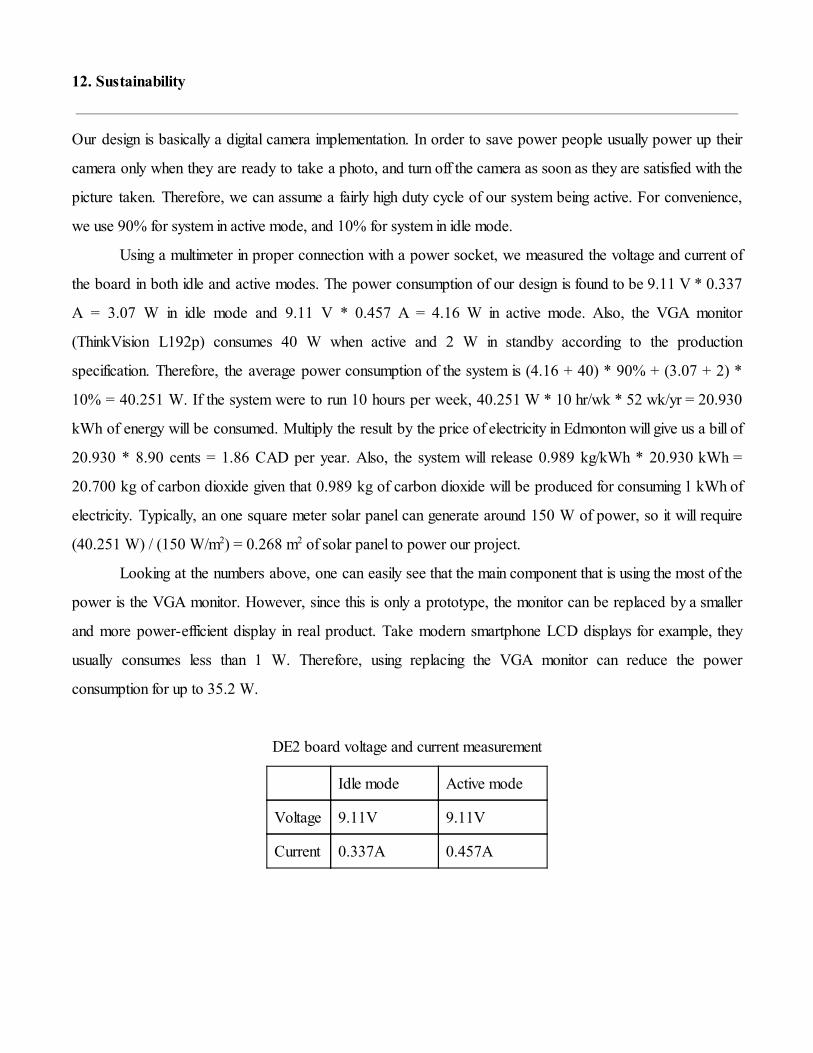
12. Sustainability
Our design is basically a digital camera implementation. In order to save power people usually power up their
camera only when they are ready to take a photo, and turn off the camera as soon as they are satisfied with the
picture taken. Therefore, we can assume a fairly high duty cycle of our system being active. For convenience,
we use 90% for system in active mode, and 10% for system in idle mode.
Using a multimeter in proper connection with a power socket, we measured the voltage and current of
the board in both idle and active modes. The power consumption of our design is found to be 9.11 V * 0.337
A = 3.07 W in idle mode and 9.11 V * 0.457 A = 4.16 W in active mode. Also, the VGA monitor
(ThinkVision L192p) consumes 40 W when active and 2 W in standby according to the production
specification. Therefore, the average power consumption of the system is (4.16 + 40) * 90% + (3.07 + 2) *
10% = 40.251 W. If the system were to run 10 hours per week, 40.251 W * 10 hr/wk * 52 wk/yr = 20.930
kWh of energy will be consumed. Multiply the result by the price of electricity in Edmonton will give us a bill of
20.930 * 8.90 cents = 1.86 CAD per year. Also, the system will release 0.989 kg/kWh * 20.930 kWh =
20.700 kg of carbon dioxide given that 0.989 kg of carbon dioxide will be produced for consuming 1 kWh of
electricity. Typically, an one square meter solar panel can generate around 150 W of power, so it will require
(40.251 W) / (150 W/m2) = 0.268 m2 of solar panel to power our project.
Looking at the numbers above, one can easily see that the main component that is using the most of the
power is the VGA monitor. However, since this is only a prototype, the monitor can be replaced by a smaller
and more power-efficient display in real product. Take modern smartphone LCD displays for example, they
usually consumes less than 1 W. Therefore, using replacing the VGA monitor can reduce the power
consumption for up to 35.2 W.
DE2 board voltage and current measurement
Idle mode Active mode
Voltage 9.11V 9.11V
Current 0.337A 0.457A
13. References
[1] “Worldwide Smartphone Shipments Top One Billion Units for the First Time” IDC 04/08/2014 https://www.idc.com/getdoc.jsp?containerId=prUS24645514
[2] “Smartphones killing point-and-shoots, now take almost 1/3 of photos”
GIGAOM 04/08/2014 http://gigaom.com/2011/12/22/smartphones-killing-point-and-shoots-now-take-almost-13-of-photos/
[3] C328-7640 JPEG Camera Module W/ UART Interface datasheet:
Sparkfun, COMedia Ltd. 03/03/2014
http://www.sparkfun.com/datasheets/Sensors/Imaging/C328.pdf
[4] C328-7640 JPEG Camera Module W/ UART Interface datasheet user manual:
Sparkfun, COMedia Ltd. 03/03/2014
http://www.sparkfun.com/datasheets/Sensors/Imaging/C328_UM.pdf
C328-7640 Camera driver / API:
[5] appnotes from Shinichiro Nakamura, mbed 03/03/2014
http://mbed.org/cookbook/CameraC328
[6] appnotes from Zachary Byrne 03/03/2014
http://www.ece.ualberta.ca/~elliott/ece492/appnotes/2010w/Interfacing_C328_Camera_Module/
[7] Terasic D5M Camera Hardware Specification:
Terasic Technologies Inc. 08/04/2014
http://www.terasic.com.tw/cgi-bin/page/archive_download.pl?Language=English&No=281&FID=cbf3f0dcd
be2222a36f93826bcc25667
[8] Terasic D5M Camera User Manual:
Terasic Technologies Inc. 08/04/2014
http://www.terasic.com.tw/cgi-bin/page/archive_download.pl?Language=English&No=281&FID=09c534c7
a8354c5fa0b5fd1e72f3ed96
[9] Altera Audio/Video Configuration Core for DE-Series Boards:
Altera Corporation 08/04/2014
https://www.google.ca/url?sa=t&rct=j&q=&esrc=s&source=web&cd=1&cad=rja&uact=8&ved=0CCoQF
jAA&url=ftp%3A%2F%2Fftp.altera.com%2Fup%2Fpub%2FAltera_Material%2F12.0%2FUniversity_Pro
gram_IP_Cores%2FAudio_Video%2FAudio_and_Video_Config.pdf&ei=rnxEU77tJaaOyAGCgoEY&usg
=AFQjCNFyhPoJk79D4HPDB-43bYXIGF6EJA&bvm=bv.64507335,d.aWc
[10] Terasic D5M Camera Application notes:
ECE 492 – Winter 2014 - Group 9 Brent Erickson, Mavis Chan, Sydney Bitner 08/04/2014
https://www.ualberta.ca/~delliott/local/ece492/appnotes/2014w/G9_Terasic_D5M_Camera/
[11] 16-bit (RG565) colour and 8-bit grayscale format:
The Imaging Source Europe GmbH. 03/03/2014
http://www.imagingcontrol.com/en_US/support/documentation/class/PixelformatRGB565.htm
[12] Altera Embedded Peripherals IP User Guide
Altera Corporation 08/04/2014
https://www.google.ca/url?sa=t&rct=j&q=&esrc=s&source=web&cd=1&cad=rja&uact=8&ved=0CDkQF
jAA&url=http%3A%2F%2Fwww.altera.com%2Fliterature%2Fug%2Fug_embedded_ip.pdf&ei=I3lEU6H
OG6GwygHEv4DQCQ&usg=AFQjCNEzXym_nGgj854k_Jxq3HpLfLcIIQ&bvm=bv.64507335,d.aWc
[13] Altera Video IP Cores for Altera DE Series Boards
Altera Corporation 08/04/2014
https://www.google.ca/url?sa=t&rct=j&q=&esrc=s&source=web&cd=1&cad=rja&uact=8&ved=0CCoQF
jAA&url=ftp%3A%2F%2Fftp.altera.com%2Fup%2Fpub%2FAltera_Material%2F9.1%2FUniversity_Prog
ram_IP_Cores%2FAudio_Video%2FVideo.pdf&ei=43lEU7KkAe66yAGRn4DYDw&usg=AFQjCNH-V
Bt9cVeonn4AAPI-E1QR-5qB_w&bvm=bv.64507335,d.aWc
[14] “Spectral colour image processing”
Ravindranath, M. R&D, CMC Ltd., Hyderabad, India, Bhagvati, C. ; Deekshatulu, B.L. 03/03/2014
http://ieeexplore.ieee.org/xpl/articleDetails.jsp?tp=&arnumber=6108962&queryText%3DColour+Image+Pr
ocessing
[15] “colour Image to Grayscale Image Conversion”
Saravanan, C. Nat. Inst. of Technol., Comput. Centre, Durgapur, India 03/03/2014
http://ieeexplore.ieee.org/xpl/articleDetails.jsp?tp=&arnumber=5445596&queryText%3DGrayscale+Image+
Processing
SD card driver:
[16] Appnotes from Jason Brown & Brady Thornton 03/03/2014
https://www.ualberta.ca/~delliott/local/ece492/appnotes/2013w/SD_card_interfacing/
[17] Altera University Program Secure Data Card IP Core 08/04/2014
https://www.google.ca/url?sa=t&rct=j&q=&esrc=s&source=web&cd=1&cad=rja&uact=8&ved=0CCoQF
jAA&url=ftp%3A%2F%2Fftp.altera.com%2Fup%2Fpub%2FAltera_Material%2F11.0%2FUniversity_Pro
gram_IP_Cores%2FMemory%2FSD_Card_Interface_for_SoPC_Builder.pdf&ei=_IJEU-DRIOewyQH6y
4GABQ&usg=AFQjCNET6uEtwYDAu9C5Zc1gr-kBBy0c5w&bvm=bv.64507335,d.aWc
[18] ECE 492 Lab tutorials and reference materials of Altera
Altera Corporation & Nancy Minderman & Duncan Elliott 03/03/2014
https://eclass.srv.ualberta.ca/course/view.php?id=11728
Ethernet and Web server:
[19] appnotes Brent Erickson & Mavis Chan & Sydney Bitner 03/03/2014
https://www.ualberta.ca/~delliott/local/ece492/appnotes/2014w/G9_ETHERNET/
[20] DM9000A Ethernet IP core 08/04/2014
https://www.ualberta.ca/~delliott/local/ece492/appnotes/2013w/Ethernet_DM9000A/DM9000A.tar
[21] Datasheet for the DM9000A Ethernet:
DAVICOM Semiconductor, Inc. 08/04/2014
http://www.cs.columbia.edu/~%20sedwards/classes/2013/4840/Davicom-DM9000A-Ethernet-controller.pd
f
[22] Web Page Design:
bootstrap.css 08/04/2014
http://getbootstrap.com/css/
[23] BMP file converter:
2009 lidaibin 08/04/2014
http://code.google.com/p/libbmp/
[24] Altera University Program RS232 UART
Altera Corporation 08/04/2014
https://www.google.ca/url?sa=t&rct=j&q=&esrc=s&source=web&cd=1&cad=rja&uact=8&ved=0CCoQF
jAA&url=ftp%3A%2F%2Fftp.altera.com%2Fup%2Fpub%2FAltera_Material%2F11.1%2FUniversity_Pro
gram_IP_Cores%2FCommunications%2FRS232.pdf&ei=9qRFU--SBMTQyAHSpYCwDg&usg=AFQjC
NFDPFYeAyXq3IK6l2QINw6rs-O7gw&bvm=bv.64507335,d.aWc
[25] HTML reference:
W3Schools, Refsnes Data. 08/04/2014
http://www.w3schools.com/html/default.asp
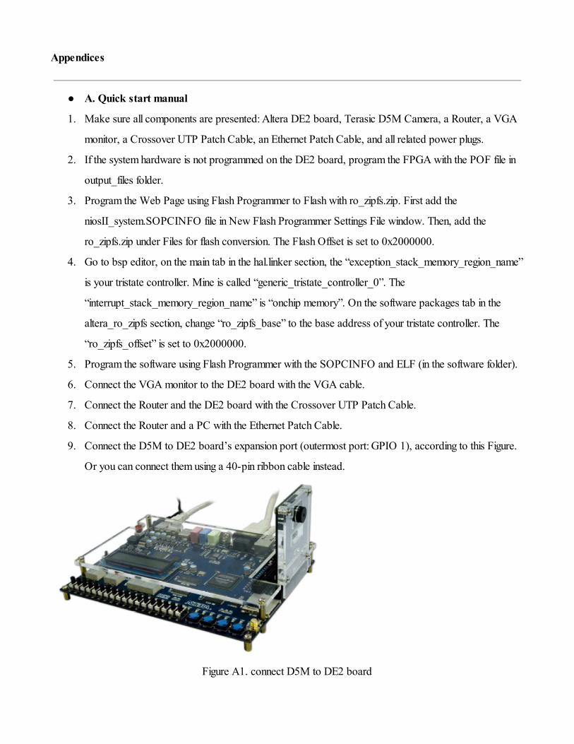
Appendices
● A. Quick start manual
1. Make sure all components are presented: Altera DE2 board, Terasic D5M Camera, a Router, a VGA
monitor, a Crossover UTP Patch Cable, an Ethernet Patch Cable, and all related power plugs.
2. If the system hardware is not programmed on the DE2 board, program the FPGA with the POF file in
output_files folder.
3. Program the Web Page using Flash Programmer to Flash with ro_zipfs.zip. First add the
niosII_system.SOPCINFO file in New Flash Programmer Settings File window. Then, add the
ro_zipfs.zip under Files for flash conversion. The Flash Offset is set to 0x2000000.
4. Go to bsp editor, on the main tab in the hal.linker section, the “exception_stack_memory_region_name”
is your tristate controller. Mine is called “generic_tristate_controller_0”. The
“interrupt_stack_memory_region_name” is “onchip memory”. On the software packages tab in the
altera_ro_zipfs section, change “ro_zipfs_base” to the base address of your tristate controller. The
“ro_zipfs_offset” is set to 0x2000000.
5. Program the software using Flash Programmer with the SOPCINFO and ELF (in the software folder).
6. Connect the VGA monitor to the DE2 board with the VGA cable.
7. Connect the Router and the DE2 board with the Crossover UTP Patch Cable.
8. Connect the Router and a PC with the Ethernet Patch Cable.
9. Connect the D5M to DE2 board’s expansion port (outermost port: GPIO 1), according to this Figure.
Or you can connect them using a 40-pin ribbon cable instead.
Figure A1. connect D5M to DE2 board
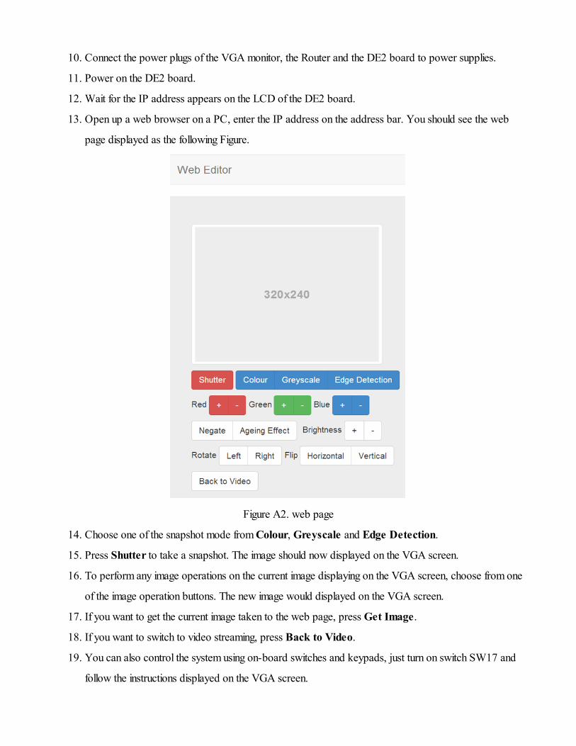
10. Connect the power plugs of the VGA monitor, the Router and the DE2 board to power supplies.
11. Power on the DE2 board.
12. Wait for the IP address appears on the LCD of the DE2 board.
13. Open up a web browser on a PC, enter the IP address on the address bar. You should see the web
page displayed as the following Figure.
Figure A2. web page
14. Choose one of the snapshot mode from Colour, Greyscale and Edge Detection.
15. Press Shutter to take a snapshot. The image should now displayed on the VGA screen.
16. To perform any image operations on the current image displaying on the VGA screen, choose from one
of the image operation buttons. The new image would displayed on the VGA screen.
17. If you want to get the current image taken to the web page, press Get Image.
18. If you want to switch to video streaming, press Back to Video.
19. You can also control the system using on-board switches and keypads, just turn on switch SW17 and
follow the instructions displayed on the VGA screen.
● B. Future work
1. The prototype uses Ethernet with a router as the communication media between the board and the
mobile devices. This can be further improved by replacing Ethernet with a Wi-Fi module.
2. The current version of the on-board editor only has instructions printed out as plain text. A simple GUI
for the on-board editor could be made for better user experience.
3. The software implementation of image operations can be shift to hardware implementation to gain
processing speed accelerations. Accelerate image colour processing by implementing the calculations in
VHDL with FPGA custom module. Linear equations that performs image operations can be implement
with adders, subtractors and multipliers in VHDL, image buffer manipulation which copying bytes from
one array to another can also accelerate in custom VHDL modules, so that the operation can be done in
parallel (a line of bytes together) instead of moving byte by byte in a loop of software.
4. Provide user options to choose image resolution, or choose the camera output format.
5. Add more colour image operations such as: wavelength flipping, smoothing, and image enhancements.
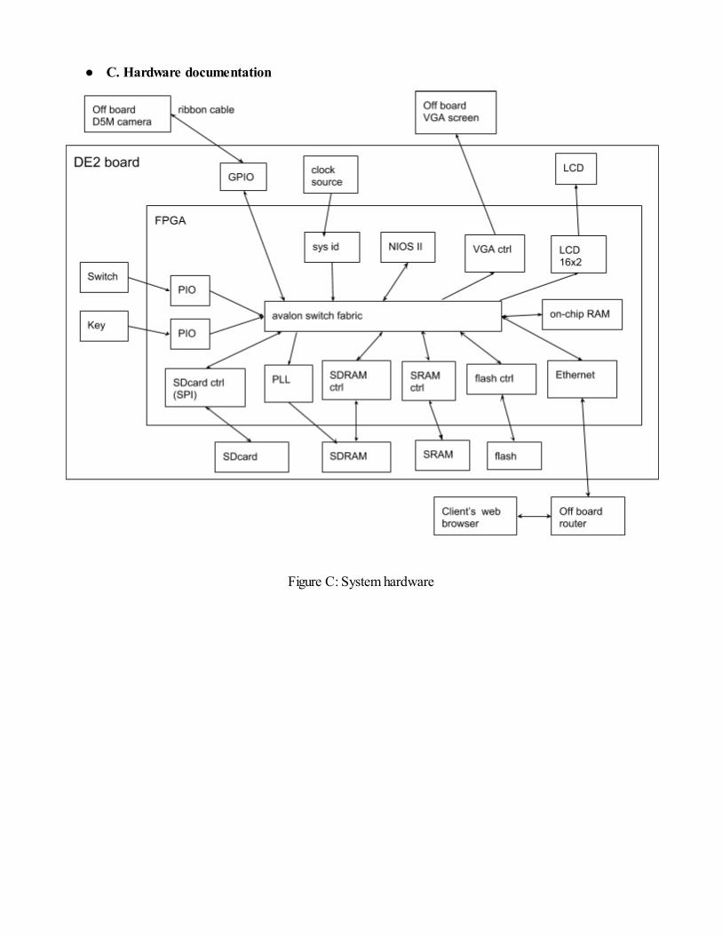
● C. Hardware documentation
Figure C: System hardware
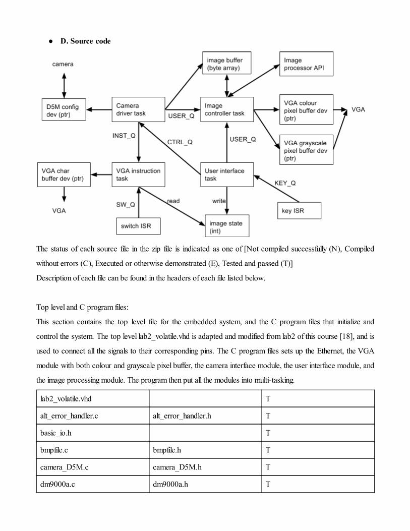
● D. Source code
The status of each source file in the zip file is indicated as one of [Not compiled successfully (N), Compiled
without errors (C), Executed or otherwise demonstrated (E), Tested and passed (T)]
Description of each file can be found in the headers of each file listed below.
Top level and C program files:
This section contains the top level file for the embedded system, and the C program files that initialize and
control the system. The top level lab2_volatile.vhd is adapted and modified from lab2 of this course [18], and is
used to connect all the signals to their corresponding pins. The C program files sets up the Ethernet, the VGA
module with both colour and grayscale pixel buffer, the camera interface module, the user interface module, and
the image processing module. The program then put all the modules into multi-tasking.
lab2_volatile.vhd T
alt_error_handler.c alt_error_handler.h T
basic_io.h T
bmpfile.c bmpfile.h T
camera_D5M.c camera_D5M.h T
dm9000a.c dm9000a.h T
dm9000a_regs.h T
http.c http.h T
image_operator.c image_operator.h T
network_utilities.c T
sd_write.c T
srec_flash.c T
user_interface.c user_interface.h T
web_server.c web_server.h T
Web Editor:
This section contains all the files needed to create the web editor. In our web editor, we used a styling library
from Bootstrap [22]. defaultImage.bmp is provided for displaying a welcome message when the page is first
loaded. index.html and not_found.html are the standard html files that define the web editor. A minified jquery.js
javascript library is also included for proper styling of the web editor.
bootstrap.css T
bootstrap.js T
defaultImage.bmp T
index.html T
jquery.js T
not_found.html T
Hardware implementations of image operation functions:
As mentioned in section 9.2 Comparison of Image Operations Using Software and Hardware Implementation.
We have tried to implement image operation functions in VHDL hardware, but there are almost no speedup
comparing to software. The files below are not included in the compiled binaries of our system.
CCW_Index.vhd C
CW_Index.vhd C
IMG_Color_Dec.vhd C
IMG_Color_Inc.vhd C
IMG_Gray_Dec.vhd C
IMG_Gray_Inc.vhd C
IMG_Negate.vhd C
RFH_Index.vhd C
RFV_Index.vhd C