Embed Size (px)
Citation preview

Degree project in
IGCT Transient Analysis and ClampCircuit Design for VSC valves
SANCHIT SINGH
Stockholm, Sweden 2012
XR-EE-E2C 2012:014
Electrical EngineeringMaster of Science
IGCT Transient Analysis and Clamp CircuitDesign for VSC valves
AuthorSanchit Singh
Company Supervisor
Senior Specialist. Ingemar Blidberg
Examiner and Supervisor at Institute
Prof. Hans-Peter Nee
Master ThesisDepartment of Electrical Energy Conversion
School of Electrical EngineeringRoyal Institute of Technology (KTH)
Stockholm, Sweden 2012XR-EE-E2C 2012:014


Abstract
IN today’s high power VSCs (Voltage Source Converters), IGBTs (Insulated Gate Bipolar Transistors)are the dominant semiconductors. These converters are in general modular multilevel based and
contain several building blocks that are series connected. Each of these building blocks in turn con-sist of several series connected IGBT valves. One of the advantages of using modular multilevel basedVSCs is the ability to switch each building block at a lower frequency compared to the average totalswitching frequency of the converter. IGBTs generally have lower switching losses than other semi-conductors, however, their on-state losses are higher because of a larger on-state voltage. Furthermore,series connection of IGBTs devices imposes voltage sharing complications that are generally difficultto deal with. A solution to this problem is to increase the amount of series connected building blocksand thus avoid series connection of semiconductors. To lower the semiconductor on-state losses, ei-ther the IGBTs are replaced by improved IGBT and drives or an alternative semiconductor that ismore suited for modular multilevel topologies can be used. In this thesis, an alternative semiconductorcalled IGCT (Integrated Gate-Commutated Thyristor) is studied; more specifically RC-IGCT (ReverseConducting IGCT). An analytic analysis is conducted to grasp the switching behavior, furthermore, asimulation model in Pspice R© is proposed for confirming the analytic analysis. This model is also usedfor parameter sweeps of clamp circuit components from which a table is created. This table can be usedfor comprehending the effects of changing values on the switching transient and also for the design ofclamp circuit components. However, a numerical and a graphical method together with the Pspice R©
model are proposed for designing the clamp circuit. It is found that the graphical method is far moreintuitive and revealing than the numerical. If further accuracy is required, then the graphical methodcan be used in tandem with the numerical. A fault case analysis of the clamp circuit is conducted inorder to reveal how failures in the clamp components affect the semiconductors and other componentsin a building block. Some of these failures are more destructive than others. The IGCT building blockstates and current paths are discussed and finally series connection of IGCTs is considered.
i


Sammanfattning
IDagens högeffekt VSC:er (Voltage Source Converter), IGBT:er (Insulated Gate Bipolar Transistor) ärdominanta halvledare. De här omvandlare är generellt modulär multi-nivå baserade och innehåller
flertal block som är seriekopplade. Varje block i sin tur består av ett antal seriekopplade IGBT:er. En avfördelarna med att använda modulär multi-nivå omvandlare är möjligheten att kunna switcha enskildablock med lägre frekvens än den totala medelfrekvensen av omvandlaren. IGBT:er har generellt lägreswitchförluster än andra halvledare, dock har de oftast högre ledförluster. Seriekoppling av IGBT:erär komplicerad ur spänningsdelnings perspektive samt svårare att hantera än tillämpningar utan se-riekoppling. En lösning till detta problemet är att öka antal block i omvandlare, vilket leder till attseriekoppling kan undvikas. För att lösa det andra problemet med höga ledförluster kan man antingenersätta IGBT:er med förbättrade versioner eller så kan man använda alternativa halvledare. I det härexjobbet, en alternativ halvledare som heter IGCT (Integrated Gate-Commutated Thyristor) studeras;mer specifikt RC-IGCT (Reverse Conducting IGCT). En analytisk analys genomförs för att få insikti switchförloppen samt en simuleringsmodell förslåss för att bekräfta den analytiska analysen. Dennaföreslagna modellen används även till parametriska simuleringar av klampkrets komponenter för attskapa en tabell. Tabellen används för att förstå hur ändringar i komponentvärden påverkar switchför-loppen samt även används för att designa klampkrets komponenter. En design procedur som användersig av en numerisk metod och en grafisk method tillsammans med simuleringar föreslåss. Man kom-mer fram till att grafiska metoden är helt klart mer intuitiv samt mer avslöjande än den numeriskametoden. Om mer noggrannhet önskas, kan grafiska metoden tillsammans med numeriska metodenanvändas. Ett felfall analys genomförs för att ta reda på hur felen i klampkretsen påverkar de övrigakomponenterna i blocken. Vissa av dessa fel är mer destruktiva än andra. IGCT block tillstånd ochströmbanor diskuteras och slutligen seriekopping av IGCT:er undersöks.
iii


Acknowledgments
The completion of this master thesis has only been possible through support from numerous individ-uals. I would like to take the opportunity to express my gratitude towards the following individuals:
• Professor Hans-Peter Nee for accepting the supervision of this thesis.
• Senior Specialist Ingemar Blidberg at ABB HVDC for:
– Accepting me for this thesis.
– Providing support, constructive feedback and discussions in both the report and thesiswork.
• Annika Lokrantz at ABB HVDC for providing with detailed and constructive feedback on thereport.
• Jim Liljekvist at ABB HVDC for:
– showing interest in my thesis.
– Being there to listen to my thoughts and ideas.
– Providing with constructive comments and his own ideas.
I would also like to thank the members of the department for making the work experience pleasantand enjoyable.
Lastly, I would like to thank my family for providing moral support and motivation throughout myeducation at KTH.
v


Table of Contents
Abstract i
Sammanfattning iii
Acknowledgments v
Table of Contents vii
Introduction 1
1. IGCT Introduction 71.1. Considering IGCT as Valve . . . . . . . . . . . . . . . . . . . . . . . . . . . . . . . . . . . . . . . 71.2. IGCT Basics . . . . . . . . . . . . . . . . . . . . . . . . . . . . . . . . . . . . . . . . . . . . . . . . . 71.3. IGCT Transient Waveform and Terminology . . . . . . . . . . . . . . . . . . . . . . . . . . . 11
2. Analytic Circuit Analysis 132.1. Circuit Introduction and Terminology . . . . . . . . . . . . . . . . . . . . . . . . . . . . . . . . 132.2. Motivation for the Clamp Circuit . . . . . . . . . . . . . . . . . . . . . . . . . . . . . . . . . . . 142.3. Transient Analysis . . . . . . . . . . . . . . . . . . . . . . . . . . . . . . . . . . . . . . . . . . . . . 142.4. Clamp Circuit Energy Losses . . . . . . . . . . . . . . . . . . . . . . . . . . . . . . . . . . . . . . 162.5. Selecting Choke Inductor Li1 . . . . . . . . . . . . . . . . . . . . . . . . . . . . . . . . . . . . . . 172.6. Selecting Clamping Diode . . . . . . . . . . . . . . . . . . . . . . . . . . . . . . . . . . . . . . . . 182.7. Selecting Rs and CC L . . . . . . . . . . . . . . . . . . . . . . . . . . . . . . . . . . . . . . . . . . . 18
3. Circuit simulations 233.1. Selecting Simulation Program . . . . . . . . . . . . . . . . . . . . . . . . . . . . . . . . . . . . . . 233.2. Modeling Test Circuit . . . . . . . . . . . . . . . . . . . . . . . . . . . . . . . . . . . . . . . . . . . 243.3. IGCT Transient Simulation . . . . . . . . . . . . . . . . . . . . . . . . . . . . . . . . . . . . . . . 263.4. Parameter Sweeps . . . . . . . . . . . . . . . . . . . . . . . . . . . . . . . . . . . . . . . . . . . . . . 28
4. Design Procedure Example 314.1. Problem Description . . . . . . . . . . . . . . . . . . . . . . . . . . . . . . . . . . . . . . . . . . . 314.2. Analytical Start Point . . . . . . . . . . . . . . . . . . . . . . . . . . . . . . . . . . . . . . . . . . . 314.3. Simulation Confirmation and final Adjustments . . . . . . . . . . . . . . . . . . . . . . . . . . 354.4. Result Summary and Discussion . . . . . . . . . . . . . . . . . . . . . . . . . . . . . . . . . . . . 36
5. Clamp Circuit Fault Cases 395.1. Clamp Inductor Li1’s Effect . . . . . . . . . . . . . . . . . . . . . . . . . . . . . . . . . . . . . . . 405.2. Clamp Resistor Rs ’s Effect . . . . . . . . . . . . . . . . . . . . . . . . . . . . . . . . . . . . . . . . 405.3. Clamp Capacitor CC L’s Effect . . . . . . . . . . . . . . . . . . . . . . . . . . . . . . . . . . . . . 415.4. Clamp Diode DC L’s Effect . . . . . . . . . . . . . . . . . . . . . . . . . . . . . . . . . . . . . . . . 425.5. Summary of Critical Fault Cases . . . . . . . . . . . . . . . . . . . . . . . . . . . . . . . . . . . . 44
vii

viii Table of Contents
6. IGCT MMC Building Block States and Current Paths 476.1. Commutation between diode and IGCT . . . . . . . . . . . . . . . . . . . . . . . . . . . . . . . 476.2. States and Current Paths . . . . . . . . . . . . . . . . . . . . . . . . . . . . . . . . . . . . . . . . . 48
7. Considering Series Connection of IGCTs 517.1. Transient Voltage Balancing . . . . . . . . . . . . . . . . . . . . . . . . . . . . . . . . . . . . . . . 517.2. Static Voltage Balancing . . . . . . . . . . . . . . . . . . . . . . . . . . . . . . . . . . . . . . . . . 527.3. Simulations . . . . . . . . . . . . . . . . . . . . . . . . . . . . . . . . . . . . . . . . . . . . . . . . . . 537.4. Series Connection Conclusion . . . . . . . . . . . . . . . . . . . . . . . . . . . . . . . . . . . . . 55
Conclusion and Future Work 57
References 59
Acronyms and Terminology 61
List of Figures 66
List of Tables 67
Appendix 69
A. Clamp Circuit Analytic Analysis 71A.1. Inductor Current . . . . . . . . . . . . . . . . . . . . . . . . . . . . . . . . . . . . . . . . . . . . . . 71A.2. Capacitor Voltage . . . . . . . . . . . . . . . . . . . . . . . . . . . . . . . . . . . . . . . . . . . . . 73A.3. Capacitor Peak Voltage and Peak Time . . . . . . . . . . . . . . . . . . . . . . . . . . . . . . . . 74A.4. Zero Inductor Current Time . . . . . . . . . . . . . . . . . . . . . . . . . . . . . . . . . . . . . . 75
B. Example Data sheet of an IGCT 77

Introduction
IN the early days of electrical engineering, DC (Direct Current) system was the only type of transmis-sion system known to mankind and it was in use between 1870s and 1880s. In the late 1880s, the AC
(Alternating Current) transmission system emerged and overwhelmed DC. Even though AC-systemhas been the norm for quite some time now, DC-system has continued to evolve in the shadows. From1930s and onwards, a rising demand for power paved the way for HVDC (High Voltage Direct Cur-rent) as an alternative for transmission of high power from remote localities[1]. Today at ABB, HVDCis promoted in two different forms, HVDC Classic and HVDC Light1.
HVDC Light is a self-commutated VSC (Voltage Source Converter) based technology. It is a successfuland environmental friendly way of designing a power transmission system. HVDC Light is speciallybeneficial when it comes to supplying power to offshore platforms, connecting offshore wind farms,improving grid reliability, city infeed and powering islands[1]. As of now, the converter stations usestate of the art turn-on/turn-off IGBT (Insulated-Gate Bipolar Transistor) as valves (see Figure 0.1 fora simplified diagram of a HVDC with VSC).
IGBT Valves
Figure 0.1.: Simplified single-line diagram for HVDC with voltage source converters[2].
Some benefits of HVDC Light over conventional HVDC Classic are[1, 2]:
• Compact and light-weight design.
• Rapid control of both active and reactive power independently of each other to keep voltage andfrequency stable.
• Reactive power can be controlled at terminals without being dependent on dc transmission volt-age level.
• Converters can be placed almost anywhere in the AC system.
1Siemens has an equivalent product called HVDC Plus.
1

2 Introduction
• Permits black start; i.e. converter can behave as a synchronous generator.
• Converters demand no reactive power.
• There is no restriction on minimum network short-circuit capacity.
• No relevant electromagnetic fields.
Taking the above mentioned benefits of HVDC Light into consideration, one can conclude that it hasa promising future as can alternative to the conventional HVDC system. The reason why HVDCLight hasn’t completely replaced HVDC Classic is due to technical limitation at very high powertransmission, cost effectiveness and because losses are still higher at the same power level.
HVDC Light Generations
HVDC Light has been in constant development since 1997. The generation number simply representsimprovements in terms of cost and loss reduction made in the development of HVDC Light since thelast generation.
Generation 1
Generation 1 technology emerged in 1997[3]. It is based on two-level topology (see Figure 0.2 for asimplified diagram of a two-level converter topology) and promises converter losses of no more than3%[4]. To keep the current ripple low, a high switching frequency is used and filters are required todamp harmonic distortions.
+
-
dU
dU
Figure 0.2.: Simplified single-line diagram of a Two-level converter.
Generation 2
Generation 2 emerged in 2002 and is based on a three-level topology (see Figure 0.3 for a simplifieddiagram of a three-level converter topology)[4]. This technology permits a lower switching frequency(thus reducing switching losses) and promises converter losses of no more than 1.8% at the cost of in-creased component cost[3]. The conversion reduces the stresses on the filter compared with generation1 due to improved harmonic generation.
Generation 3
Generation 3 was introduced in 2005; this generation promised losses of no more than 1.4%, but thistechnology utilized the two-level converter topology once again[4]. Loss reduction was achieved byoptimized IGBT and drive, and OPWM (Optimized Pulse-Width Modulation) with lower switchingfrequency. Thus, harmonic generation was kept at the same level as generation 2.

Introduction 3
dU
+
-
dU
Figure 0.3.: Simplified single-line diagram of a Three-level converter.
Generation 4
It is based on MMC2 (Modular Multilevel Converter) (see Figure 0.4 for a simplified diagram of a MMCtopology). It promises reduced switching losses, with total converter losses down to 1%. Almost nofiltering is required and it is easily scalable to high voltages. One of the main reasons for loweredswitching losses and filtering stresses is that, that even though the effective switching frequency of theconverter is very high, each building block is switched at a much lower frequency[5].
-
+dU
dU
Figure 0.4.: Simplified single-line diagram of a MMC.
2ABB calls its MMC for CTL, because it is a little different in some aspects[5].

4 Introduction
Trend Today
Today, work is underway in this field to minimize the losses of HVDC Light further and at the sametime increase the power capacity such that it is comparable to HVDC Classic. This goal can be achievedby using numerous methods. One such method is to replace today’s IGBT valves with improved IGBTvalves and control strategies or use a different semiconductor.
Purpose
The purpose of this thesis is to study an alternative semiconductor called IGCT (Integrated Gate-Commutated Thyristor) for the converter valves. Only recently, developments in the field of IGCTshave improved the Safe Operating Area (SOA)[6] and made IGCT an attractive candidate as valves inthe converters. ABB HVDC have limited experience in handling IGCTs and one significant part ofthe study is to comprehend IGCT; its basic structure and functionality.
The category of IGCT that this thesis will mainly discuss is called RC-IGCT (Reverse ConductingIntegrated Gate-Commutated Thyristor). The study will contain the following aspects:
• The turn-on and turn-off behavior.
• The effect of surrounding electrical components on the switching transients on MMC buildingblock level.
• Optimizing the clamp circuit for a given maximum DC-capacitor voltage and turn-off load cur-rent.
• Study of behavior in fault cases.
• Understanding states and current paths of an IGCT MMC building block.
• Considering series connection of IGCTs.
Scope
To meet the goals of the study, following steps will be taken:
• Get sufficient knowledge of the layout of a typical GCT.
• Comprehend the turn-on and turn-off behavior of the GCT part using semiconductor physics.
• Find a suitable program for simulation of the RC-IGCT with its clamp circuit.
• Comprehend the commutation process between IGCT and diode using heuristic reasoning andconfirmation using simulations.
• Conduct an analysis to determine the model robustness and accuracy.
• Understand how changes in the clamp circuit parameters and stray inductances affect transientbehavior through parameter sweeps.
• Use the information from the above step to determine the criteria for optimum performance.
• Determine the optimum clamp circuit parameters for a given DC-voltage and maximum turn-offload current.
• Use simulation to determine how the performance of IGCT circuit is affected during differentclamp circuit fault cases.

Introduction 5
• Consider an IGCT MMC building block and discuss the commutation process, the differentstates and current paths.
• Understand how IGCT can be series connected and discuss the advantages and disadvantages ofdoing so.


CHAPTER1IGCT Introduction
THE IGCT is introduced including why it is considered to be a suitable candidate as a valve in themodern day converter valves, its internal structure and the different categories of IGCTs available
today. Furthermore, a study is conducted in order to understand the switching behavior of the GCTpart of the IGCT. Lastly, switching waveform terminology and definitions are introduced
1.1. Considering IGCT as Valve
IGCT is a power semiconductor that can be considered as an improvement to the more commonGate Turn-off Thyristor (GTO). IGCT was commercially introduced in 1997 and its main applicationdomains were Industrial Drives, Traction and Energy Management. After just 5 years of its introduc-tion, IGCT established itself as the power semiconductor of choice for high power level applications,because of lower costs, higher reliability and efficiency[7]. In general, IGBT’s are more cost effec-tive at high powers and high frequencies. Free Wheeling Diodes (FWD) are fast and IGBT losses are,in comparison with other devices such as GTO and IGCTs, low. However, IGCTs are better suitedfor still higher powers but lower switching frequencies[8]. The superiority of IGCTs is noticeable athigher powers. In the on-state, IGCT generally has a smaller on-state voltage and hence lower lossesin this mode compared to an IGBT of the same voltage and current class. Lower switching frequenciesare required due to higher turn-on and turn-off energies of IGCTs.
High power applications require series connection of semiconductor devices since these devices canblock only a limited amount of voltage. Even though, there has been some success earlier with seriesconnection of IGCT’s in high power applications[9], it is still considered to be a more difficult venturein comparison with series connection of IGBTs[10]. This is one of the reasons as to why IGCT hasn’testablished itself as THE power semiconductor of choice for VSC valves. Recent trends however arepointing towards dismissing series connection of power semiconductors altogether[11] and instead usemany more cells3 in the MMC (see Figure 0.4). In MMCs, lower switching frequencies are employedand voltage step is scalable in individual converters. Furthermore, preliminary loss calculations[12]point towards IGCT being an attractive valve for this category of converters.
1.2. IGCT Basics
1.2.1. Structure
GCT refers to the semiconductor press-pack component. The additional I in the abbreviation hasits origin from the special fabrication which involves integrating gate unit in a very low inductance ar-rangement. IGCT is fabricated like a GTO and allows for unity gain turn-off of the thyristor structure.
3Also called MMC building block.
7
8 Chapter 1. IGCT Introduction
In the vertical direction, it utilizes exclusive techniques such as buffer-layer and transparent emitter forloss reduction. The buffer-layer technology is implemented in many power semiconductors (GCTs,GTOs, power diodes and IGBTs). This technologies allows for 30% reduced thickness at the same for-ward voltage, thus, on-state losses and turn-off losses are reduced significantly. Typically, buffer-layerdevices require larger trigger currents at turn-on, to avoid this problem transparent anode emitter tech-nology is used. At turn-off this technology allows for equivalent performance as through conventionalanode shorts. Additionally the structure allows for monolithic integration of an anti-parallel diode inthe same wafer[8, 13, 14] (see Figure 1.1).
DiodeGCT
np
n
n n
p
p
Figure 1.1.: Schematic of the separation region of GCT and its diode part[13].
There are several categories of IGCTs available today[15]:
RC-IGCTs reverse conducting IGCTs with anti-parallel diode integrated in the same wafer4 (see Figure 1.2).
RB-IGCTs reverse blocking IGCTs
A-IGCTs asymmetric IGCTs that neither allows for reverse conduction or reverse blocking.
Figure 1.2.: RC-IGCT with its gate-unit mounted on the same circuit board[16].
4This thesis will focus mainly on this type.

1.2. IGCT Basics 9
1.2.2. GCT Operation
1.2.2.1. Turn-on
In the turn-on mode, GCT behaves exactly like a thyristor (or a GTO). This operation principle can beunderstood by considering the equivalent two-transistor model given in Figure 1.45. The p+n− p andn+ pn− regions represent PNP and NPN transistors respectively. The anode of the GCT is connectedto p+ region, which is the emitter of the PNP transistor. The collector of the PNP is connected tothe gate of the NPN transistor and vice-versa, because of n− region neighboring the p region. Thecathode of the GCT is connected to the n+ region, which is the emitter of the NPN transistor[13].
This two-transistor model has two stable states, ON and OFF, which are determined by the gate con-trol. When a current is supplied to the gate to turn on the GCT, the gate current flows to the cathodeThis turns on the NPN transistor and its collector current will now flow from the anode through theJ1 junction. The J1 junction is the emitter of the PNP transistor, therefore, the collector current ofthe PNP is then the base current of the NPN. The two transistors are connected in positive feedbackallowing for a self-sustaining state called latch-up. This state is reached because the large current flow-ing between the anode and cathode is able to inject enough carriers into the base regions to keep thetransistors saturated without the need of continuous gate current flow[17, 18] (Figure 1.4 illustratesthe different stages of the turn-on process using the two-transistor equivalent circuit). Typical turn-ontime for a GCT is about ≈ 10µs[19].
A
G
Cp buffern basen basep n
1J 2J 3J
Figure 1.3.: One-dimensional structure of GCT.
G
Stage 1 Stage 2 Stage 3
G
A
C
1J
2J
2J
3JG
A
C
1J
2J
2J
3J
A
C
1J
2J
2J
3J
Figure 1.4.: Two-transistor equivalent model of the GCT and its turn-on stages.
5This model can be derived from the basic one-dimensional structure in Figure 1.3.

10 Chapter 1. IGCT Introduction
1.2.2.2. Turn-off
The turn-off mode, however, differs from that of a GTO. A GTO is turned off by negative currentinjection into the NPN base. Once the base current is reduced to a certain level, the collector currentand hence the PNP base current reduces. This in turn, reduces the collector current of the PNP,leading to a further reduction in the base current of the NPN base[17]. This positive feedback processturns-off the GTO. The majority of the anode current flows out from the cathode and only a fractionof anode current flows out from the gate that is why the turn-off gain βo f f = IA/IG of the GTO is ofthe order 3∼ 5[19].
To turn-off a GCT, all the anode current is diverted to the gate, causing the cathode current to decreaserapidly. At the time cathode current decreases to a level close to zero, the minority carriers associatedwith the gate-cathode junction (J3) are removed. At zero cathode current, minority carrier injectionfrom n+ side into the p base seizes[17]. Now, the GCT is an open base PNP transistor (Figure 1.5illustrates the turn-off process using the two-transistor equivalent circuit). Typical turn-off time of aGCT is about ≈ 20µs [19].The time it takes for the current to commutate to the gate is of the order∼ 1µs . This short time constricts the maximum allowable stray inductance of the gate unit. A typical
value of the stray inductance of the gate-unit assuming VG = 20V andd i
d t= 1000A/µs , is
Ls <VG
d i/d t=
20
1000· 1µs = 20nH (1.1)
This tight constraint on the stray inductance is one of the reasons why the gate unit is required to beintegrated in a low-inductance arrangement with the GCT[13].
Since all the current flows from the anode to the gate the turn-off gain βo f f of the GCT is unity. Theunity gain is advantageous because it significantly shortens the storage time6 compared to that of aGTO. Other advantages of unity gain are improvement in the SOA of the GCT and the abridged needfor snubber circuits[13].
Stage 1 Stage 2 Stage 3
G
A
C
1J
2J
2J
3JG
A
C
1J
2JOpen-base
2J
3JG
A
C
1J
2J
2J
3J
Figure 1.5.: Two-transistor equivalent model of the GCT and its turn-off stages.
6Time required to remove minority carriers from the p-base.

1.3. IGCT Transient Waveform and Terminology 11
1.3. IGCT Transient Waveform and Terminology
The typical waveforms of the turn-on and turn-off transients are given in Figure 1.6. The terminologyused in the figure is explained below:
VD static on-state voltage, typically the dc-link capacitor voltage in a building block.
IT is the constant forward load current.
ITGQM is the maximum current that the IGCT can turn-off.
diT
dtis the rate of rise of the forward load current.
VDSP is the first peak of the IGCT (see Figure 1.6); depends upon its characteristics and strayinductances.
VDM is the second peak of the IGCT (see Figure 1.6); depends upon external clamp circuit.
CS is the electrical command signal sent to the gate unit (GU).
SF is the electrical status-feedback signal.
tdon is the turn-on delay time. Similarly, td o f f is the turn-off delay time.
tdon SF turn-on status-feedback time. Similarly, td o f f SF is the turn-off status feedback time.
tr is the anode voltage fall time.
Figure 1.6.: Typical IGCT turn-on and turn-off waveforms[15].


CHAPTER2Analytic Circuit Analysis
TEST circuit used for transient analysis is introduced. Later, a thorough theoretical analysis of theclamp circuit is covered; including optimizing the clamp circuit for a given DC capacitor voltage
and maximum turn-off load current.
2.1. Circuit Introduction and Terminology
To test the turn-on and turn-off transients, and for finding suitable clamp circuit parameter values, astandard test circuit is used. This circuit can be found in the data sheets for IGCTs and is commonlyused for switching events occurring in a Voltage Source Inverter (VSI), be it a 2-level or 3-level topology.This circuit with all the stray inductances is given in Figure 2.17 including standard terminology for thecomponents. The terminology is further explained below[15]:
CDCLink is the dc-link capacitor, which is the main energy storage unit in a building block of aMMC.
Li2 is the stray inductance of the CDC Li nk .
F W D is the free-wheeling diode (FWD), which is the anti-parallel diode of the second IGCT,commonly found in a half-bridge topologies.
Li1 is the choke inductance used for limiting d iT /d t through the FWD.
Rs is the clamp resistor, it is used to dissipate the energy stored in Li1.
Ls is the stray inductance of Rs .
CCL is the clamp capacitor, used for clamping the over-voltage caused by the large Li1.
VCL is the CC L voltage.
DCL is the clamp diode. Used for conducting the energy stored in Li1 to Rs and CC L.
DUT is the Device Under Testing (DUT), in our case, it is the IGCT.
LCL is the overall stray inductance of the loop CC L-DC L-DU T -F W D .
Lload is the load inductance.
Rload is the load resistance.
7In essence, this circuit is a buck-converter[18].
13

14 Chapter 2. Analytic Circuit Analysis
sR
DCLinkC
CLD DUT
FWDloadL
CLL1iL
loadRsL
2iL
CLC
Figure 2.1.: Test circuit for the IGCT including all the modeled stray inductances.
2.2. Motivation for the Clamp Circuit
As mentioned previously, the circuit in Figure 2.1 is mainly used for studying turn-on and turn-offtransients but it can also be used for finding suitable values for the clamp circuit parameters Li1, Rsand CC L using computer simulations. But then the question arises, why is there a need for a clampcircuit?
For simplicity let’s assume that the only stray inductance in the test circuit is LC L and that the onlycomponents used in Figure 2.1 are CDC Li nk , DU T , F W D and Ll oad . Capacitor CDC Li nk is charged tothe level VD , IGCT isn’t conducting and the load current IT is free-wheeling through FWD. From ourdiscussions in subsection 1.2.2, we know that the rate of turn-on of the IGCT isn’t controllable, hence,when we turn-on the IGCT the d iT /d t is much larger than what the FWD is designed for. Thislimit forces us to use a choke inductor Li1 to turn-off FWD at a rate that it can withstand. However,an inductor in series with the IGCT causes VDSP to be unnecessarily large at IGCT turn-off and caninflict damage to the component. We need to clamp this over-voltage somehow, which is achieved byusing a capacitor CC L. Inductor Li1 stores magnetic energy when the IGCT is conducting and thisenergy needs to be dissipated somewhere, otherwise it will oscillate between CC L and Li1. A clampingresistor Rs is required for dissipating this energy and a clamping diode DC L is needed to make surethat current through the FWD during its turn-off is limited mainly by Li1 and not just LC L(Figure 2.2illustrates the the need for inclusion of components in steps). The inclusion of the clamp circuitincreases the component count per building block, which is considered to be one of the disadvantagesof using IGCT as valve.
2.3. Transient Analysis
2.3.1. Turn-on
In order to proceed with the analysis of the test circuit an understanding of the waveforms givenin Figure 1.6 is needed at circuit level. We begin by considering the turn-on waveforms. Initially,let’s assume that CC L is charged to the same voltage as CDC Li nk , no current is flowing through theclamp circuit components and the load current is free wheeling through FWD. Then at some time

2.3. Transient Analysis 15
CLD
loadL
Clamp over-voltage
CLCDCLinkC
DUT
FWD
1iL
loadR
Damp oscillations/Burn energy
Fix FWD turn-offsR
CLCDCLinkC
DUT
FWD
1iL
loadR
sR
CLCDCLinkC
DUT
FWD
1iL
loadR
Limit FWD turn-off di/dt
DCLinkC
DUT
FWDloadL
1iL
loadR
DCLinkC
DUT
FWDloadL
loadR
Figure 2.2.: Motivating clamp circuit. This figure illustrates the need for inclusion of components in steps inan IGCT circuit.
t0, a command signal is sent to the IGCT to turn it on. After a short time delay, depending uponthe characteristics of the IGCT, the voltage over it drops rapidly and once it has fallen to ≈ 0.1VD , thecurrent commutation process starts. The current through FWD starts to drop at the rate that is mainlylimited by Li1 , while the current through the IGCT increases at the same rate. Figure 2.3 illustratesthe commutation process. From the figure we find that:
iF W D = iT − iu (2.1)
Commutation current iu increases from 0 to IT at the same time iF W D decreases from IT to 0. Therise rate of iu (or equivalently, fall rate of iF W D ) is determined by the largest inductance in the loop.In this case, it is Li1 that is the largest inductance.
The current overshoot in the turn-on waveform of IGCT has to do with the reverse recovery currentIRM of FWD, which in turn depends to some extent on the characteristics of the diode and the fall rateof d iF W D/d t or equivalently rise rate of d iu/d t through IGCT.
2.3.2. Turn-off
The turn-off process is more complex. Initially, let’s assume that the IGCT is turned on and is con-ducting full load current. Clamp capacitor CC L is charged to the same voltage as CDC Li nk so that DC Lis turned off. At some time t0, a command signal is sent to the IGCT to turn it off. Voltage over IGCTrises rapidly while the current drops at the rate limited only by LC L. The peak voltage VDSP definedin Figure 1.6 is dependent on the stray inductance LC L, the forward recovery voltage VF R of DC L andthe characteristics of the IGCT[15]. Figure 2.4 illustrates the simplified commutation process. Fromthe figure we find that:
iDU T = iT − iu1(2.2)

16 Chapter 2. Analytic Circuit Analysis
sR
DCLinkC
CLD DUT
FWDloadL
CLL1iL
loadR
CLC
ui
Ti
2iL
FWDi
Figure 2.3.: Redrawn test circuit during commutation from FWD to IGCT excluding some stray inductancesfor simplicity.
Commutation current iu1increases from 0 to IT while iDU T decreases from IT to 08. From the figure
we can also notice that it is only LC L that limits the d i/d t of the commutation current. CapacitorCC L initially gets charged by iu1
and once iT has commutated over to FWD, the currents in the clampcircuit is governed by the equivalent parallel resonance circuit of Figure 2.69. Figure 2.5 illustrates thecurrents in the test circuit after commutation. The capacitor voltage appears over IGCT, since DC Lis conducting. The voltage overshoot VDM is the maximum charge voltage of CC L; the value of VDMdepends highly on the chosen Rs , CC L, Li1 and stray inductances. Once DC L stops conducting, whichoccurs when iLi1
decreases at the rate that is governed by the parallel resonance circuit to zero, thevoltage across the IGCT oscillates down to VD . Capacitor voltage vC L decays with a time constantτ = Rs CC L until it reaches the same static value as the IGCT. The total time it takes for the capacitorto discharge to VD depends on the chosen Rs , CC L, Li1 and stray inductances.
2.4. Clamp Circuit Energy Losses
A huge choke inductor can always be found in IGCT circuits to limit the turn-off d i/d t of FWD andthis inductor stores a significant amount of magnetic energy depending on the transient mode of thecircuit. At IGCT turn-off, the stored magnetic energy from the on-state of the IGCT is given by:
ERs=
I 2T Li1
2(2.3)
While, at IGCT turn-on , the stored magnetic energy from the reverse recovery of the FWD is givenby:
ERs=
I 2RM Li1
2(2.4)
8the effects of the IGCT tail current is neglected here since it is quite small and shouldn’t have any significant influence onthe clamp circuit.
9See section 2.7 for an explanation of why the clamp circuit can be approximated as a parallel resonance circuit after thecurrent commutation from IGCT to FWD.

2.5. Selecting Choke Inductor Li1 17
sR
DCLinkC
CLD DUT
FWD loadL
CLL1iL
loadR
CLC1ui
Ti2iL
DUTi
Figure 2.4.: Redrawn test circuit during commutation from IGCT to FWD excluding some stray inductancesfor simplicity.
sR
DCLinkC
CLD DUT
FWD loadL
CLL1iL
loadR
CLCTi
2iL
1iLi
CLCi
sRi
Figure 2.5.: Currents in the test circuit after commutation from IGCT to FWD.
Both of these energies are burned in Rs . This is true for a simple loss calculation model, however,according to [20] not all of this magnetic energy is burned in Rs some of it is burned in the semicon-ductors and some is restored back to the CDC Li nk .
2.5. Selecting Choke Inductor Li1
To ensure safe turn-off of FWD, Li1 needs to be dimensioned appropriately. To do that, we considerthe circuit in Figure 2.3 again. Using Kirchoff’s Voltage Law (KVL) through the iu current loop of thefigure, we get:

18 Chapter 2. Analytic Circuit Analysis
VD max − Li2d iT max
d t− Li1
d iT max
d t− LC L
d iT max
d t= 0⇒ (2.5)
Li1 >−Li2− LC L+VD max
d iT max/d t
where VD max is the maximum CDC Li nk voltage that will be used and d iT max/d t is the maximum turn-off decay rate allowed for the FWD, this is usually specified in corresponding data sheets. As one cannotice from the equation above. The value of Li1 is influenced only by stray inductances, maximumCDC Li nk voltage and the d iT max/d t of FWD. It is independent of the maximum turn-off current. Aswe’ll see later on in this chapter, the values of Rs and CC L are influenced by the turn-off current.
2.6. Selecting Clamping Diode
When selecting DC L for the clamping circuit, the Forward Recovery VF R of the diode needs to betaken into account. This over-voltage has a direct effect on the voltage across the IGCT during turn-off. This effect can be understood by having another look at Figure 2.4. In the figure, the effect of LC Lis an increase in VDSP and since the commutation current iu1 flows through both LC L and DC L thevoltage across DC L also contributes to a increase in VDSP . The VF R depends mainly on the voltageclass, diameter of the wafer, the temperature and the forward d i/d t .
In summary, DC L should be chosen such that it has the smallest VF R possible and at the same timeshould be of the same voltage class as the IGCT[15].
2.7. Selecting Rs and CC L
2.7.1. Analytical Relationships
Since the test circuit contains stray inductances and diodes it can be very difficult to find an analyticsolution using circuit differential equations. One has to turn to simulations for a more reliable circuitbehavior. It is however possible to find analytic relationships during IGCT turn-off to aid in dimen-sioning Rs and CC L
10 by making a few assumptions[21]. From these assumptions we get the simplifiedcircuit given in Figure 2.6.
The circuit in Figure 2.6 is actually a parallel resonance circuit. A thorough analysis of this circuitis given in Appendix A. We are interested in only a few characteristics of this circuit. According toFigure 1.6 and subsection 2.3.2, we are interested in the following specific characteristics:
• The time tmax it takes for vC L to reach its maximum value. This is equivalent to the time it takesfor IGCT to reach VDM .
• The maximum value of CC L voltage Vmax , where Vmax =VDM .
• The time tend it takes for the LC L current to become zero. This is relevant because we want toknow the time it takes for DC L to turn-off[15].
10The value of Li1 is fully dependent on the current decay rate d iT /d t that the FWD is designed to withstand, as discussedin section 2.5.

2.7. Selecting Rs and CC L 19
sR
1iL
CLC
1iLi
CLCi
sRi
CLvFigure 2.6.: The simplified clamp circuit based on the assumptions above.
All of the above mentioned characteristics can be extracted from Appendix A, they are included herefor convenience:
4CC LR2s
Li1> 1 (2.6)
tmax =1
ωdtan−1
ωd
σ
(2.7)
Vmax = iT
s
Li1
CC Le− σωd
tan−1ωd
σ
(2.8)
tend =π
ωd− tmax (2.9)
where,
ωd =q
ω2n −σ
2 (2.10)
ωn =1
p
Li1CC L
(2.11)
σ =1
2Rs CC L(2.12)
From the above relationships, we can deduce that tmax is independent of the turn-off voltage andcurrent, it only depends on Li1, CC L and Rs . Since Li1 is decided by the maximum current derivativeas discussed in section 2.5 we only have two degrees of freedom here. The voltage Vmax = VDM isproportional to the turn-off current, by decreasing CC L, we can decrease VDM at the cost of changingthe values of tmax and tend .
2.7.2. Parameter Optimization
Clamp circuit parameter values, Rs and CC L must be chosen with respect to some optimization con-straints. In order to find a mathematical representation for these constraints, we need to identify the

20 Chapter 2. Analytic Circuit Analysis
SOA limitations. During IGCT turn-off, we are interested in minimizing VDSP , VDM and to f f −mi n ,in order for the IGCT to meet the specified SOA[15]. The time to f f −mi n is given by:
to f f −mi n = ton−mi n + 2tBD with: ton−mi n ≥IT GQM + IRM
d iT /d t+ td yn (2.13)
The equations are derived using Figure 2.7. These limitations are directly related to the clamp circuit.However, there are also limitations due to the IGCT itself. This is due to the fact that the GCT needssome minimum time to reach its steady-state[15].
Figure 2.7.: Minimum dead times ton−mi n and to f f −mi n[15]
To minimize VDSP the clamp stray inductance LC L needs to be minimized. We have little control overLC L from electrical design point of view. However, VDM depends almost entirely on the parameter
values of the clamp circuit. Same is true for to f f −mi n ; in Equation 2.13 the termIT GQM+IRM
d iT /d t td yn inmany cases and td yn also depends almost entirely on the clamp circuit[15].
To minimize VDM we first need to find a mathematical representation for it, this is given in Equation 2.8.Next, since td yn is directly related to to f f −mi n , we need to find a mathematical representation for it as

2.7. Selecting Rs and CC L 21
well. Time td yn as defined in Figure 2.7 can be considered as the sum of two intervals. The first intervaltend as given in Equation 2.9 and the second tC L is the discharge time of the RC-circuit created by Rsand CC L. This time interval is defined as:
tC L =−τ ln
1−Pe r
100
(2.14)
which is derived from the basic RC-circuit discharge relationship vC L = vC L (0) e− tτ , where τ =
Rs CC L and Pe r is the percentage voltage drop. Thus, the mathematical representation of td yn is:
td yn = tend + tC L =π
ωd−
1
ωdtan−1
ωd
σ
−τ ln
1−Pe r
100
(2.15)
From NLP (non-linear programming) theory[22], we know that a general minimization problem canbe written in the form:
mi nx
f (x) (2.16)
subject to: g (x)≤ 0
where x is a vector, f (x) is the function to be minimized11 and g (x) are the constraints. In our case,
x =
Rs CC LT (2.17)
f (x) =Vmax = iT
s
Li1
CC Le− σ(x)ωd (x)
tan−1
ωd (x)σ(x)
(2.18)
g (x) = (2.19)
=
1−4CC LR2
s
Li1π
ωd (x)−
1
ωd (x)tan−1
¨
ωd (x)
σ (x)
«
−Rs CC L ln
1− Pe r100
− tend Req
≤
00
where tend Req is the maximum td yn allowed. The problem in Equation 2.16 can be solved graphicallyor numerically. In the graphical method one can choose a data set of allowed Rs and CC L and then plota range of contours of f (x) and g (x). A few contour values should be sufficient to get an approximateoptimum. Since it was already mentioned that simulations need to be conducted in order to includethe effects of stray inductances, an approximate optimum is all that may be required. Furthermore, itis much easier to comprehend if the optimum is a global or a local minimum. A program with userfriendly graphical user interface (GUI) is developed to apply the graphical method12. In the numericalmethod Matlab’s fmincon function can be used to solve the problem. This function is specially designedto solve non-linear optimization problems written in this form. There are however some disadvantageswith this method:
• An initial guess is required for the program to run.
• The problem to be solved using fmincon needs to be convex in order to guarantee a global mini-mum solution.
11also called an objective function.12see chapter 4 for an elaborate example of using this program.

22 Chapter 2. Analytic Circuit Analysis
2.7.3. Minimum Transient Time Limitation
It can be of interest to know the minimum value of td yn that can theoretically be achieved for a givenIGCT with a given maximum peak repetitive voltage (VDRM ) and a specific load current iT , since td yndirectly affects ton−mi n and to f f −mi n as discussed in the previous section. One way to extract thisvalue is to consider Equation 2.17, Equation 2.18, Equation 2.19 and interchange the last constraint inEquation 2.19 with the objective function of Equation 2.18; tend Req is removed and instead we have aVmaxReq =VDRM . So now the new optimization functions are:
x =
Rs CC LT (2.20)
f (x) = tend + tC L = td yn =π
ωd (x)−
1
ωd (x)tan−1
¨
ωd (x)
σ (x)
«
−Rs CC L ln
1−Pe r
100
(2.21)
g (x) =
1−4CC LR2
s
Li1
iT
s
Li1
CC Le− σ(x)ωd (x)
tan−1
ωd (x)σ(x)
−VmaxReq
≤
00
(2.22)
This problem can be solved using the graphical method. However, this method is very sensitive tothe initial guess; there are a lot of local minimum candidates and it can be very difficult to find aninitial guess that gives the optimum solution. A recommended method is to use the graphical one asmentioned in the previous subsection.

CHAPTER3Circuit simulations
A simulation model for the test circuit used in this thesis is introduced. Next, the theoretical analysisof chapter 2 is confirmed including the effects of stray inductances. Lastly, parameter sweeps are
used to create a table that aids in comprehending the effects of changing parameter values on theswitching transients.
3.1. Selecting Simulation Program
Once a theoretical base has been established one needs to confirm theory with practice. The cheapestalternative is to use computer simulations. A first step is to find an appropriate program to conductsimulations in. A study was conducted to find a suitable program for simulations of the test circuit.The results of the study is summarized in Table 3.1.
The choice of the program was based on the following criteria:
• Familiarity with the program is recommended but not a necessary condition.
• The program should allow for running multiple simulations with different component values,also called Parameter Sweep.
• The program should have support for transient analysis.
• It is highly desirable for the program to be widely accepted for power electronics simulations.With this characteristic, simulations will be reliable and consistent.
Taking the above criteria into consideration we can conclude that Pspice R© is the suitable candidate.
Table 3.1.: Summary of the survey of suitable simulation programs. Orange marked header represents theprogram of choice.
Matlab R© Pspice R© Microcap R© Simplorer R© PSCAD R©
Adv-
antages
Disadv-
antages
Adv-
antages
Disadv-
antages
Adv-
antages
Disadv-
antages
Adv-
antages
Disadv-
antages
Adv-
antages
Disadv-
antages
Easy toplot
graphsand set
axisscalingusingcode.
Firstsimulation
inSimPowerSystemstoolboxgave in-
consistentresults.
First sim-ulationgaveresultsthatweredeci-pher-ableand
consis-tent.
Not muchcontrol
over thestyle ofplotting
andscaling of
axis.
Is spicebased
andeasierto usethan
Pspice R© .
Hierarchialmodelsare notpossible
to createin Micro-
cap.
Containsa lot offeatures
thatboth
Matlab R©
andPspice R©
provide.
Model forIGCT isn’tavailable.
Unfamiliarwith this
program.
23

24 Chapter 3. Circuit simulations
Possibleto runsimula-tions in
afor-loop
andchange
morethan onparam-
etereveryitera-tions.
Is meantfor systemanalysis,
onlysimplepower
electron-ics
modelsare
available.
Parametersweepcan beused toiteratevalues
ofcompo-nents, isalmost
as pow-erful as
Matlab R© .
There areno
modelsavailablefor powerelectron-
icscompo-nents in
Pspice R©
library.
Easy tochangeplotting
styleand
scalingof axis.
Unfamiliarwith this
program.
Possibleto
pausesimula-
tionand
changevalues
ofcompo-nents.
Unfamiliarwith this
program.
Meant forsystemanalysisand not
fordetailed
analysis ofcircuit
compo-nents.
There isa possi-bility tocheckcurve
forms inrealtimeusing
“Scope”in
simulinklibrary.
Notpossibleto pausesimulation
andchangevalues.
ManyIEEE re-
searchershaveused
P-spicefor cre-ating
modelsfor
powerelec-
tronicscompo-nents.
Notpossibleto pause
thesimulation
andchangevalues.
Otheradvan-tagesare
similarto
Pspice R© .
Otherdisadvan-tages aresimilar toPspice R© .
Simulationsin realtime
are pos-sible.
Not aspopular
asPspice R©
fortransient
analysis ofsmall tomediumelectricalcircuits.
Familiarwith this
pro-gram.
Has areputa-tion of
being agood
tool fortran-sient
analysisof small-medium
sizedelectri-
calcircuits.
Real timesimulationresults are
notpossible.
There isno
needfor
speciallicenses
tocreate
newmodels.
Familiarwith this
pro-gram.
Speciallicense isneeded
forcreating
newmodels.
3.2. Modeling Test Circuit
Once a simulation platform has been selected a suitable simulation model needs to be considered. Themain purpose of the simulations is to confirm the theoretical analysis of chapter 2 and also examine theeffects of stray inductances in Figure 2.1. For this category of simulations, modeling the exact turn-offbehavior of the IGCT isn’t of utmost importance. Thus, IGCT can be modeled as an ideal switch withdefined turn-on and turn-off transient times[15].
3.2.1. GCT Model
In Pspice R© an ideal switch with editable model is called Sbreak. The editable parameters are Ron ,Ro f f , Von and Vo f f . The total voltage across IGCT during conduction is given by[18]:

3.2. Modeling Test Circuit 25
Vcond =VT + IT rT (3.1)
where VT is the nominal on-state voltage (see Appendix B), IT is the current through the IGCT13 andrT is the slope resistance (see Appendix B). From this information Ron becomes:
Ron =Vcond −VT
IT(3.2)
Ro f f is set to a large value, such as Ro f f = 1 · 104, this is because the GCT doesn’t conduct in theturn-off state. Voltage Von and Vo f f are set to 1 and 0 respectively, this is to match the V 1 and V 2parameters of the GU model.
3.2.2. GU Model
The gate unit can be modeled as a simple Vpulse in Pspice R©. Vpulse has a number of parameters thatneed to be defined in order for it to work. These parameters together with their explanations are givenbelow:
T D =Delay timeT F = Fall timeT R=Rise time
PW = Pulse-widthP ER= Period
V 1=ON voltageV 2=OFF voltage
As previously mentioned, V 1 and V 2 values are set equal to Von and Vo f f . The other parameter val-ues, except for T F and T R don’t have a significant effect on simulations and are set almost arbitrarily.The value of T F is set according to data sheets similar to the one given in Appendix B. Similarly, T Ris adjusted to match Turn-on delay time (td (on)) found in the data sheet.
3.2.3. Diode Model
The diodes in the test circuit; FWD and DC L, can be modeled using editable model Dbreak. Therelevant parameters of the Dbreak model for this application is only the (series resistance) Rs of thediode. This value is calculated using Equation 3.1 and Equation 3.2. Values of VT and rT can beextracted from data sheets similar to the one in Appendix B.
3.2.4. Further Simplifications
The load inductance Ll oad is modeled as a current generator assuming that Ll oad is very large. Thissimplification doesn’t have any influence on the turn-off transient although it does have an effect on
13Here we assume that IT is the maximum turn-off current.

26 Chapter 3. Circuit simulations
turn-on. The turn-on transient, however, isn’t as critical as the turn-off and hence this simplificationis acceptable. The other simplification made in this circuit is the CDC−Li nk , this is modeled as an idealDC-voltage generator. This simplification is valid when assuming the voltage over this capacitor to beclose to ripple free.
3.2.5. Pspice R© Test Circuit
Utilizing the discussion in the previous sections a working simulation model such as the one given inFigure 3.1 can be created. This model is valid for clamp circuit design and for examining the effects ofstray inductances only[15]. It doesn’t model the complex IGCT turn-on and turn-off in detail or thereverse recovery of the power diodes FWD and DC L.
5
5
4
4
3
3
2
2
1
1
D D
C C
B B
A A
<Doc> <RevCode>
<Title>
A
1 1Thursday, June 21, 2012
Title
Size Document Number Rev
Date: Sheet of
0
0
DclampDCL
FWDFWD
VDC3300Vdc
+-
+
-
IGCT
DUT
Ls
LS1 2
Lcl
LCL1 2
I11800Adc
Li2
LI2
1
2
Li1
Li1
1 2
GATE
TD = TDTF = TFPW = 3e-3PER = 6e-3V1 = 0TR = TRV2 = 1
Rload
1e-9
CCLCCL
Rs
RS
PARAMETERS:
TF = 5e-6
TD = 0TR = 4.8e-6RS = 0.77
CCL = 7.6u
Li1 = 6.5uLCL = 200nLI2 = 50nLS = 125n
Figure 3.1.: Pspice R© model of the test circuit.
3.3. IGCT Transient Simulation
3.3.1. IGCT Turn-on
To test the functionality of the simulation model, a first simulation of IGCT turn-on is conducted.The result of one such simulation is given in Figure 3.2. The turn-on waveforms in this figure are quitesimilar to the one given in Figure 1.6. The reverse recovery of the FWD during IGCT turn-on isn’tmodeled and hence the current overshoot isn’t visible.
To verify the commutation discussion in subsection 2.3.1 one can plot the current through LC L and Li1in the same figure. As one can notice from Figure 3.3 the same commutation current flows throughthem and the derivative is determined by Li1 as required for safe operation of the FWD.

3.3. IGCT Transient Simulation 27
emiT
5.95ms 5.97ms 5.99ms 6.01ms 6.03ms 6.05ms 6.07ms 6.09ms1 IDUT 2 VDUT
0A
0.40KA
0.80KA
1.20KA
1.60KA
1.81KA1
0V
1.00KV
2.00KV
3.00KV
4.00KV
5.00KV
5.43KV2
>>
Figure 3.2.: Current through the IGCT (DUT) and the voltage across it during turn-on.
emiT
5.96ms 5.98ms 6.00ms 6.02ms 6.04ms 6.06ms 6.08ms 6.10ms1 I(Lcl) I(Li1) 2 D(I(Li1)) D(I(Lcl))
0A
0.40KA
0.80KA
1.20KA
1.60KA
1.85KA1
-100M
0
100M
200M
300M
400M
500M2
>>
Figure 3.3.: Current through Li1, LC L and their derivatives during IGCT turn-on.

28 Chapter 3. Circuit simulations
3.3.2. IGCT Turn-off
A turn-off simulation resulting plot is given in Figure 3.4. As can be noticed from this figure, the turn-off waveform closely matches with the typical waveforms in Figure 1.6. The tail current of the IGCTisn’t modeled and hence not visible in the simulation. Furthermore, the first peak VDSP isn’t perfectlyreliable since GCT physical characteristics weren’t modeled. The second peak VDM however is reliablesince it only depends on the clamp circuit.
emiT
3.006ms 3.008ms 3.010ms 3.012ms 3.014ms 3.016ms 3.018ms 3.020ms 3.022ms1 IDUT 2 VDUT
0A
0.400KA
0.800KA
1.200KA
1.600KA
1.816KA1
0V
1.00KV
2.00KV
3.00KV
4.00KV
5.00KV
5.45KV2
>>
Figure 3.4.: Current through the IGCT (DUT) and the voltage across it during turn-off.
To verify the commutation discussion in subsection 2.3.2 one can again plot the current through Li1and LC L in the same figure. As one can notice from Figure 3.5, the current through LC L decreaseswith a derivative that is much larger than the derivative through Li1, which is in accordance with thediscussion in the section just mentioned.
3.4. Parameter Sweeps
One approach towards an understanding of how changing clamp circuit component values affect theturn-on and turn-off behavior of the IGCT is to use parameter sweeps. A parameter sweep is a type ofsimulation in which a chosen component’s value is varied for a defined number of simulations and theresulting waveforms are plotted in the same figure. In this way, hopefully, a rough relationship can beextracted.
For the test circuit simulation case we are interested in the effect of varying parameters on the followingcharacteristics:
• IGCT turn-off losses.
• Rs losses.

3.4. Parameter Sweeps 29
emiT
2.95ms 2.97ms 2.99ms 3.01ms 3.03ms 3.05ms 3.07ms 3.09msI(Li1) I(Lcl)
0A
0.4000KA
0.8000KA
1.2000KA
1.6000KA
1.8343KA
Figure 3.5.: Current through Li1, LC L and their derivatives during IGCT turn-off.
• Time it takes for CC L to discharge i.e. tC L.
• Time it takes for DC L to turn-off i.e. tend .
• td yn = tC L+ tend
• VDM
• VDSP
An example parameter sweep is given in Figure 3.6. Using the simulation results similar to the one inthe figure just mentioned together with the characteristics of interest, Table 3.2 can be created. Thistable aids in understanding the effects of increasing clamp circuit component values, verify the analyticanalysis in subsection 2.3.2 and at the same time can be used to make final adjustments to the clampcircuit design14.
Table 3.2.: Effect of IGCT turn-off.
``````````````Influence onIncrease of RS CC C L Li1 Li2 LS LC L
GCT turn-off losses → → → → RS losses → → → →
Time for CC L to discharge → →Time for DC L to turn-off →
td yn →VDM →VDSP → → → → →
→ No noticeable effect. Slight increase. Increase. Slight decrease. Decrease.
14In chapter 4 this table is used for exactly this purpose.

30 Chapter 3. Circuit simulations
emiT
2.970ms 2.980ms 2.990ms 3.000ms 3.010ms 3.020ms 3.030ms 3.040msIDUT VDUT
0
2.0K
4.0K
6.0K
8.0K
Li1Increasing values of
Sweep Li1
Start Value 500nHEnd Value 10µHIncrement 2µH
Li1Parametric Sweep of
IGCT Turn-o
Figure 3.6.: Parameter sweep of Li1 at IGCT turn-off for checking the effects on the IGCT’s voltage andcurrent waveforms.

CHAPTER4Design Procedure Example
THE purpose of this chapter is to use the knowledge gained from the previous chapters and applythat knowledge to a design problem. This example doesn’t give any suggestion on choosing
DC L and it doesn’t take any physical limitations imposed by the values of the clamp components intoaccount. Furthermore, a graphical and a numerical method for designing and optimizing the clampcircuit implemented in Matlab R© are introduced.
4.1. Problem Description
Suppose that we are to design a clamp circuit for an IGCT (whose data sheet can be found in Appendix B)that minimizes VDM given the following specifications:
1. IT max = 1600[A], the maximum current to turn-off.
2. VD max = 3300[V ], the maximum DC-link voltage allowed.
3. Maximum fall rate of FWD (found in the Diode Data section of Appendix B) i.e. d iT max/d t =510[A/µs]. The stray inductances are LC L = 300[nH ] and Li2 = 50[nH ] and Ls = 125[nH ] .
4. The minimum value of td yn should be found and chosen to be as small as possible while fulfillingVDM =Vmax t ot <VDRM
15. Where VDRM = 5.5[kV ] according to the data sheet in Appendix B.
5. Vmax t ot =VDM < 5.3[kV ] including margin and the effects of stray inductances for safe opera-tion of the IGCT.
Here, we assume the clamping diode DC L to be ideal.
4.2. Analytical Start Point
4.2.1. Choke Inductor
The first step of the design procedure is to calculate the value of Li1. This is done using Equation 2.5and from this we get:
Li1 >−50 · 10−9− 300 · 10−9+3300
510· 1 · 10−6⇒
Li1 > 6.1[µH ]
15Here Vmax t ot =Vmax +VD max
31

32 Chapter 4. Design Procedure Example
We need to include some margin when choosing a value for Li1. This is done to ensure that the FWDdoesn’t get damaged, however, one should choose a Li1which is as small as possible to get a smallervalue of VDM and td yn as one can conclude using Table 3.2. A suitable value is:
Li1 = 6.5[µH ] (4.1)
4.2.2. Minimizing td yn
The next step is to find the smallest value of td yn achievable given the specifications above. This isdone to ensure that to f f −mi n is as small as possible as discussed in subsection 2.7.2. To calculate thisvalue, the numerical method can be used according to the suggestion outlined in subsection 2.7.3. Here,a graphical method is used since it is much more reliable and intuitive. When the program is executedusing Matlab R© the GUI is launched (see Figure 4.1 for a screenshot and description of the various fieldsin the GUI).
Figure 4.1.: OptimizeClamp program GUI.
To plot the contour graph, the following data was entered in the text fields:
• Assuming an interval of interest for Rs to be
0.1Ω 5Ω
and step size to be 0.01[Ω].
• Assuming an interval of interest for CC L to be
0.1µF 30µF
and step size to be 0.01[µF ].
• Assuming an interval of interest for Vmax contour values to be
200V 2200V
and step size tobe 200[V ].
• Assuming an interval of interest for td yn contour values to be
9µs 100µs
and step size to be20[µs].
• Assuming the definition of RC-circuit’s total discharge to be 99% .
• IT max = 1600[A] according to the specification above.

4.2. Analytical Start Point 33
• Li1 = 6.5[µH ] as discussed in the previous subsection.
The above values may need to be changed if the contour plot doesn’t convey enough information.After clicking Update Graph in the program, a contour graph given in Figure 4.2 is drawn. As onecan notice from the figure, there is a contradictory trade-off involved here. When trying to minimizeVmax , td yn will need to increase and vice-versa.. In this particular example (according to item 4 insection 4.1) we are interested in minimizing td yn and at the same time keep VDM = Vmax < VDRM ,which for this example is Vmax =VDRM −VD max = 5500− 3300= 2200[V ].
Figure 4.2.: Contour plot in the program used for clamp optimization. The red shaded area represents theundamped oscillation Rs and CC L pairing according to Equation 2.6. This is the region we want to avoid.When the mouse is moved to this invalid area the values of Vmax and td yn turn red as an indication tothe user that these values are invalid.
By using the zoom tools of the program and the Value Panel, one can easily find an approximateminimum of td yn . At Vmax = 2200[V ] the IGCT could be damaged hence, a margin needs to beincluded. Furthermore, stray inductances in the circuit will also contribute to an increase in Vmax .Figure 4.3 shows the optimal values including a 100[V ] margin16. In summary, the optimum (in thecontext of minimizing td yn while keeping Vmax <VDRM ) using OptimizeClamp program was foundto be:
16Note that this margin may change depending on the application. This value was chosen arbitrarily for illustration purpose.

34 Chapter 4. Design Procedure Example
td yn ≈ 15[µs] (4.2)
Vmax ≈ 2100[V ] (4.3)Rs ≈ 1.9[Ω] (4.4)
CC L ≈ 0.66[µF ] (4.5)
Figure 4.3.: Approximate optimal values using OptimizeClamp Program.
4.2.3. Minimizing Vmax
In the previous subsection we found that the minimum td yn one can achieve in this particular designis approximately 15[µs]. It is now of interest to search for the minimum Vmax given td yn to bemaximum 15[µs]. For this optimization, the numerical method as mentioned in subsection 2.7.2 isused. As initial values for CC L and Rs , we can use the values close to the ones given in Equation 4.4and Equation 4.5 respectively. Using the following command
[CCL,Rs,Vmaxtot,tendD,tendC,exitflag,output]=OptimizeClampNum([1e-6,2],1600,3300,6.5e-6,15e-6),
in Matlab R© to run the function used in the numerical approach, we find the optimum (in the contextof minimizing Vmax and keeping td yn less than or equal to 15[µs]) to be:
4.3. Simulation Confirmation and final Adjustments 35
CC L ≈ 0.75[µF ] (4.6)Rs ≈ 1.9[Ω] (4.7)
tend ≈ 8.3[µs] (4.8)td yn ≈ 15[µs] (4.9)
Vmax t ot ≈Vmax +VD max ≈ 2053+ 3300= 5.35[kV ] (4.10)
Figure 4.4 which is one of the outputs from OptimizeClampNum.m function illustrates iLi1(t ), iC L (t ),
vC L (t ) and marks Vmax and tend on the graph.
0 0.5 1 1.5 2 2.5
x 10−5
−2000
−1500
−1000
−500
0
500
1000
1500
2000
2500
Time [s]
Am
pli
tud
e
i L i1( t)
vCL ( t)
i CL ( t)
Vmax = 2053.7796[V ], tmax = 2 .3976e− 006[s]
tendD = 8 .355e− 006[s]
Figure 4.4.: Plot of iLi1, iC L and vC L with some important points marked such as Vmax , tmax and tend marked.
4.3. Simulation Confirmation and final Adjustments
Once a theoretical optimum has been found, it needs to be confirmed using computer simulations.Computer simulation will aid in taking the effect of stray inductances on transients into account andcan also will be used to make final adjustments to the design if necessary.
We begin by using the results from Equation 4.6, Equation 4.7 and plug them into the Pspice R© sim-ulation file to confirm the results given in Equation 4.8, Equation 4.9 and Equation 4.10. Simulationresults are shown in Figure 4.5. As one can notice from the encircled value in the figure, td yn is veryclose to the value that was found in Equation 4.9. Values Vmax t ot and tend can be confirmed in similarfashion. In summary, the simulation results were found to be:
td yn ≈ 15[µs]
Vmax t ot ≈ 5.38[kV ]tend ≈ 8.96[µs]

36 Chapter 4. Design Procedure Example
A1:(3.0220m,3.3019K) A2:(3.0069m,3.3014K) DIFF(A):(15.066u,466.313m)emiT
3.00400ms 3.00800ms 3.01200ms 3.01600ms 3.02000ms 3.02400ms 3.02800msIDCL IDUT
0A
0.5KA
1.0KA
1.5KA
2.0KA
SEL>>
VDUT VCCL0V
1.0KV
2.0KV
3.0KV
4.0KV
5.0KV
tdyn
Figure 4.5.: IGCT turn-off transient plot including the voltage and current waveforms of the IGCT (DUT) andcurrent waveform of DC L. Measured dynamic time td yn is marked with red.
One can conclude from the equations above that the value of Vmax t ot is a little larger than whatwas found using the analytical method. This value is too large according to requirement item 5 insection 4.1. Final adjustments can be made at this stage using Table 3.2. According to this table, todecrease Vmax t ot , one should decrease Rs and at the same time increase CC L. The values of Rs andCC L were adjusted to 1.7[Ω] and 0.85[µF ] respectively. This change gave the following results:
td yn ≈ 15.8[µs]
Vmax t ot ≈ 5.2[kV ]tend ≈ 10.83[µs]
As expected decreasing Vmax t ot penalizes td yn a little17.
4.4. Result Summary and Discussion
The summary of the results during the different stages of the design process is given in Table 4.1.
The utmost important lessons learned from this design example are:
• The graphical method of optimizing Rs , CC L is intuitive and reliable in the sense that local-andglobal minimums are clearly visible for a data set of interest. Furthermore, design trade-off tobe considered can clearly be extracted from the contour plot.
17see Figure 4.2 for the reason.

4.4. Result Summary and Discussion 37
• Numerical method can be used to verify the results from the graphical method and also to inves-tigate if any further minimization of Vmax is possible given a maximum td yn allowed.
• Simulations have to be conducted since stray inductances affect the parameters of interest.
• The design can be refined further in the simulation process with the aid of Table 3.2.
Table 4.1.: Summary of the results attained in the design procedure example
``````````````ParameterDesign iteration Graphical Numerical Simulation Unit
Rs 1.90 1.90 1.70 [Ω]CC L 0.66 0.75 0.85 [µF ]td yn 15.00 15.38 15.80 [µs]tend 10.00 8.96 10.83 [µs]
Vmax t ot =Vmax +VD max 5.40 5.35 5.20 [kV ]


CHAPTER5Clamp Circuit Fault Cases
IN this chapter, an analysis will be conducted to understand how a component malfunction, in termsof a short circuit or disconnection, affects the performance of the test circuit. Simulations in tandem
with heuristic reasoning is used to comprehend the effects of the faults on the remaining componentsof the test circuit.
The effect on the MMC building block discussed in the next section will be similar. The followingfault cases will be considered:
• Clamp inductor Li1
– Short circuit: can occur if the there are nicks or breaks in the insulation of the windings.
– Disconnection: can occur if the winding get’s damaged somewhere.
• Clamp resistor Rs
– Short circuit: Even though this type of failure is almost nonexistent, for most types ofresistors, this could occur in some types due to insulation issues. So this failure is studiednonetheless.
– Disconnection: a common failure mode for a resistor which can occur when the maximumpower dissipation is exceeded. They are usually designed to disconnect when this failureoccurs.
• Clamp capacitor CC L
– Short circuit: is a common failure mode for capacitor and occurs when the dielectricumages due to over-stresses in terms of over-voltages, high temperatures, harmonics etc.
– Disconnection: is an uncommon failure mode but can occur during extreme voltage stressesor when connection to the capacitor has ruptured. This failure will be studied nonetheless.
• Clamp diode DC L
– Short circuit: diodes are designed to short circuit during failure. This failure can occur forexample due to avalanche breakdown when the SOA is exceeded.
– Disconnection: is an uncommon failure mode but can occur due to a ruptured connectionto the diode. This failure will be studied nonetheless.
For simulation, the model in Figure 3.1 was used together with Sbreak connected in parallel or serieswith the component of interest to simulate short circuit and disconnection respectively.
39

40 Chapter 5. Clamp Circuit Fault Cases
5.1. Clamp Inductor Li1’s Effect
5.1.1. Short Circuit
sR
CLCDCLinkC
CLD DUT
FWDloadL
CLL
Figure 5.1.: Short circuit of Li1. Stray inductance are excluded to reduce clutter.
Before IGCT Turn-on There will only be LC L limiting the FWD turn-off and this will surely dam-age the FWD (see Figure 5.1).
Before IGCT Turn-off There shouldn’t be any significant damage done to the components (seeFigure 5.1).
5.1.2. Disconnection
Before IGCT Turn-on The current will not commutate to the IGCT. There shouldn’t be any sig-nificant damage done to the test circuit.
Before IGCT Turn-off A large d i/d t would build up a large voltage across LC L. If this voltage islarge enough it could damage the clamping diode.
5.2. Clamp Resistor Rs ’s Effect
5.2.1. Short Circuit
Before IGCT Turn-on In the ideal case i.e. ignoring stray resistances, there will be no dampingin the resonance circuit created by the CDC Li nk stray inductance Li2 and the over-voltage across CC L

5.3. Clamp Capacitor CC L’s Effect 41
1iL
CLC
DCLinkC
CLD DUT
FWDloadL
CLL
2iL
Figure 5.2.: Short circuit of Rs . Stray inductance Li2 is included since it plays a roll in the LC-resonancecircuit.
(due to the reverse recovery of FWD) will oscillate (See Figure 5.2). Simulation results in Figure 5.3illustrates this phenomenon18.
Before IGCT Turn-off The oscillations will be higher because of larger magnetic energy stored inLi1. The clamping diode DC L will not turn-off and it will be damaged at next turn-on. This is becauseonly LC L will be limiting the d i/d t . Figure 5.4 illustrates this oscillation phenomenon.
5.2.2. Disconnection
Before IGCT Turn-on There shouldn’t be any significant damage done to the components.
Before IGCT Turn-off CC L will be charged to very high voltage. Both the capacitor and the IGCTcan be damaged, since VDM will become larger than VDRM . This issue is clearly visible in Figure 5.5.
5.3. Clamp Capacitor CC L’s Effect
5.3.1. Short Circuit
Before IGCT Turn-on CDC Li nk will discharge through Rs to ground. Large amount of power willbe dissipated in Rs and it can be damaged. The current will not commutate to the IGCT.
Before IGCT Turn-off CDC Li nk will discharge through Rs to ground and can damage it. The currentwill not commutate to FWD.
18In this simulation result the effect of reverse recovery of FWD isn’t included
42 Chapter 5. Clamp Circuit Fault Cases
emiT
5.860ms 5.880ms 5.900ms 5.920ms 5.940ms 5.960ms 5.980ms 6.000ms 6.020ms 6.040ms 6.060msIDCL IDUT
0A
2.0KA
4.0KAVDUT VCCL
0V
1.00KV
2.00KV
3.00KV
4.00KV
4.82KV
SEL>>
R sShort Circuit Failure of
Before IGCT Turn-on
Figure 5.3.: Short circuit failure of Rs simulation results before IGCT turn-on. As one can notice from thisfigure, the CC L voltage keeps on oscillating.
5.3.2. Disconnection
Before IGCT Turn-on There shouldn’t be any significant damage done to the components of thetest circuit.
Before IGCT Turn-off VDSP >VDRM because CC L in this case will not help in clamping the voltageacross Li1.This over-voltage will surely inflict damage to the IGCT. Simulation result in Figure 5.6illustrates this issue.
5.4. Clamp Diode DC L’s Effect
5.4.1. Short Circuit
Before IGCT Turn-on FWD will turn-off at a d i/d t that is only limited by LC L. This will surelydamage FWD since the maximum d i/d t it is designed for will be exceeded.
Before IGCT Turn-off There shouldn’t be any significant damage done to the components of thetest circuit.
5.4.2. Disconnection
Before IGCT Turn-on There shouldn’t be any significant damage done to the components.

5.4. Clamp Diode DC L’s Effect 43
emiT
2.97ms 2.98ms 2.99ms 3.00ms 3.01ms 3.02ms 3.03ms 3.04ms 3.05ms 3.06ms 3.07ms 3.08msIDCL IDUT
0A
2.0KA
4.0KA
6.0KA
SEL>>
VDUT VCCL0V
2.0KV
4.0KV
6.0KV
7.8KVR sShort Circuit Failure of
Before IGCT Turn-o
Figure 5.4.: Short Circuit failure Rs simulation results before IGCT turn-off. As one can notice from this figure,the CC L voltage keeps on oscillating and the DC L doesn’t turn-off.
emiT
2.9680ms 2.9720ms 2.9760ms 2.9800ms 2.9840ms 2.9880ms 2.9920msIDCL IDUT
0A
2.0KA
4.0KAVDUT VCCL
0V
2.0KV
4.0KV
6.0KV
8.0KV
SEL>>
R sDisconnection of
Before IGCT Turn-o
Figure 5.5.: Disconnection failure result of Rs before IGCT turn-off. As one can notice from this figure, boththe capacitor and the IGCT voltage is very large.

44 Chapter 5. Clamp Circuit Fault Cases
Time
2.960ms 2.980ms 3.000ms 3.020ms 3.040ms 3.060ms 3.080ms 3.100msIDCL IDUT
0A
2.0KA
4.0KA
SEL>>
VDUT VCCL0V
2.000KV
4.000KV
6.000KV
8.000KV
9.713KVC CLDisconnection of
Before IGCT Turn-o
Figure 5.6.: Disconnection failure CC L simulation result before IGCT turn-off. As one can notice from thisfigure, IGCT VDSP is much larger than VDRM = 6.5[kV ] for this simulation case.
Before IGCT Turn-off The over-voltage across Li1 will contribute to the VDSP peak and mightexceed VDRM . Exceeding VDRM will surely damage the IGCT.
5.5. Summary of Critical Fault Cases
Table 5.1 summarizes the critical fault cases from the analysis of the previous sections.
Table 5.1.: Clamp circuit critical fault cases and their consequences.
Nr Fault Case Consequence1 Short circuit of clamp inductor before
IGCT turn-on.Free-wheeling diode can be damaged in the
worst case.2 Disconnection of clamp inductor
before IGCT turn-off.VDSP could exceed VDRM .
3 Short circuit of clamp resistor beforeIGCT turn-off
Clamp diode will get damaged since only LC Lwill be limiting the d i/d t .
4 Disconnection of clamp resistor beforeIGCT turn-off
Clamp capacitor will be charged to a very highvoltage which is the same voltage acrossIGCT. This voltage could exceed VDRM .
5 Short circuit of clamp capacitor beforeIGCT turn-on and turn-off
Large amounts of power will be dissipated inRs , which could damage it.

5.5. Summary of Critical Fault Cases 45
6 Disconnection of clamp capacitorbefore IGCT turn-on
Voltage across clamp inductor isn’t clampedand hence VDSP could exceed VDRM .
7 Short circuit of the clamp diode beforeIGCT turn-on
Similar damage as the 1 st fault case.
8 Disconnection of the clamp diodebefore IGCT turn-off19
Similar damage as the 6 th fault case.
19A very rare case, since diodes usually short-circuit when damaged.


CHAPTER6IGCT MMC Building Block States and
Current Paths
IN this chapter, IGCT MMC building block is introduced; commutation process between diodes andIGCTs is studied and finally the states and current paths of the building block are discussed.
The circuit that will be used in this chapter is given in Figure 6.120. Before studying the states andcurrent paths, an understanding of the commutation of current between the anti-parallel diodes andIGCTs is needed.
sR
DCLinkC
CLD 1 1IGCT Diode
1iL
CLC 2 2IGCT Diode
0i
0i
Figure 6.1.: IGCT MMC building block with marked positive current convention used throughout this chap-ter.
6.1. Commutation between diode and IGCT
Commutation when i > 0 is studied, this covers the cases when the current commutates from Diode2to IGCT1 and commutation from IGCT1 to Diode221. The cases when i < 0 are not covered sincethey are very similar.
47
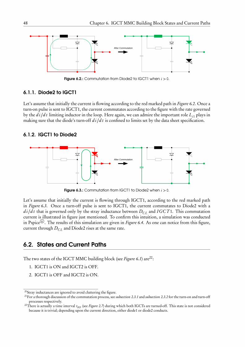
48 Chapter 6. IGCT MMC Building Block States and Current Paths
After Commutation
Figure 6.2.: Commutation from Diode2 to IGCT1 when i > 0.
6.1.1. Diode2 to IGCT1
Let’s assume that initially the current is flowing according to the red marked path in Figure 6.2. Once aturn-on pulse is sent to IGCT1, the current commutates according to the figure with the rate governedby the d i/d t limiting inductor in the loop. Here again, we can admire the important role Li1 plays inmaking sure that the diode’s turn-off d i/d t is confined to limits set by the data sheet specification.
6.1.2. IGCT1 to Diode2
After Commutation
Figure 6.3.: Commutation from IGCT1 to Diode2 when i > 0.
Let’s assume that initially the current is flowing through IGCT1, according to the red marked pathin Figure 6.3. Once a turn-off pulse is sent to IGCT1, the current commutates to Diode2 with ad i/d t that is governed only by the stray inductance between DC L and I GC T 1. This commutationcurrent is illustrated in figure just mentioned. To confirm this intuition, a simulation was conductedin Pspice R©. The results of this simulation are given in Figure 6.4. As one can notice from this figure,current through DC L and Diode2 rises at the same rate.
6.2. States and Current Paths
The two states of the IGCT MMC building block (see Figure 6.1) are22:
1. IGCT1 is ON and IGCT2 is OFF.
2. IGCT1 is OFF and IGCT2 is ON.
20Stray inductances are ignored to avoid cluttering the figure.21For a thorough discussion of the commutation process, see subsection 2.3.1 and subsection 2.3.2 for the turn-on and turn-off
processes respectively.22There is actually a time interval tBD (see Figure 2.7) during which both IGCTs are turned-off. This state is not considered
because it is trivial; depending upon the current direction, either diode1 or diode2 conducts.

6.2. States and Current Paths 49
emiT
3.005ms 3.007ms 3.009ms 3.011ms 3.013ms 3.015ms 3.017ms 3.019msIIGCT1 Idiode2 IDCL
0A
0.4KA
0.8KA
1.2KA
1.6KA
Figure 6.4.: Currents though IGCT1, Diode2 and DC L during IGCT1 turn-off
In each of these states the current can either be positive or negative. Table 6.1 summarizes all of thesestates and current paths.
Table 6.1.: IGCT MMC building block states and currents
State 1 State 2
IGCT1 ON and IGCT2 OFF If the current direction is positive than IGCT1 conducts and CDC Li nkis bypassed. The building block behaves as a short circuit in the ideal case. If however, the current is

50 Chapter 6. IGCT MMC Building Block States and Current Paths
direction is negative than Diode1 conducts and CDC Li nk is again bypassed.
IGCT1 OFF and IGCT2 ON If the current direction is positive than Diode2 conducts and CDC Li nkis charged; the building block is said to be connected. If however, the current direction is negative thanIGCT2 conducts and CDC Li nk is discharged.
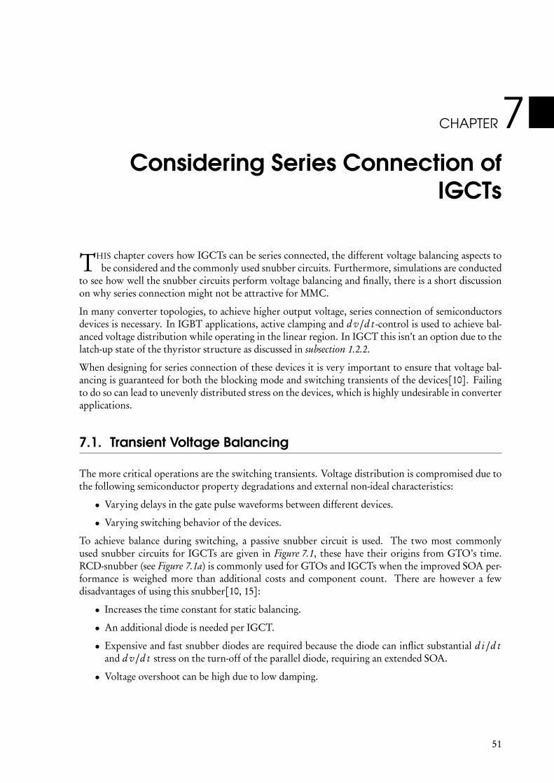
CHAPTER7Considering Series Connection of
IGCTs
THIS chapter covers how IGCTs can be series connected, the different voltage balancing aspects tobe considered and the commonly used snubber circuits. Furthermore, simulations are conducted
to see how well the snubber circuits perform voltage balancing and finally, there is a short discussionon why series connection might not be attractive for MMC.
In many converter topologies, to achieve higher output voltage, series connection of semiconductorsdevices is necessary. In IGBT applications, active clamping and d v/d t -control is used to achieve bal-anced voltage distribution while operating in the linear region. In IGCT this isn’t an option due to thelatch-up state of the thyristor structure as discussed in subsection 1.2.2.
When designing for series connection of these devices it is very important to ensure that voltage bal-ancing is guaranteed for both the blocking mode and switching transients of the devices[10]. Failingto do so can lead to unevenly distributed stress on the devices, which is highly undesirable in converterapplications.
7.1. Transient Voltage Balancing
The more critical operations are the switching transients. Voltage distribution is compromised due tothe following semiconductor property degradations and external non-ideal characteristics:
• Varying delays in the gate pulse waveforms between different devices.
• Varying switching behavior of the devices.
To achieve balance during switching, a passive snubber circuit is used. The two most commonlyused snubber circuits for IGCTs are given in Figure 7.1, these have their origins from GTO’s time.RCD-snubber (see Figure 7.1a) is commonly used for GTOs and IGCTs when the improved SOA per-formance is weighed more than additional costs and component count. There are however a fewdisadvantages of using this snubber[10, 15]:
• Increases the time constant for static balancing.
• An additional diode is needed per IGCT.
• Expensive and fast snubber diodes are required because the diode can inflict substantial d i/d tand d v/d t stress on the turn-off of the parallel diode, requiring an extended SOA.
• Voltage overshoot can be high due to low damping.
51

52 Chapter 7. Considering Series Connection of IGCTs
snubC
pR
snubD snubR
(a) RCD-snubber.
snubC
pRsnubR
(b) RC-snubber.
Figure 7.1.: IGCT commonly used snubbers with static voltage balancing resistor.
To avoid these issues a simple RC circuit can be used (see Figure 7.1b). These are common when theadditional losses are weighed less than the additional component count and SOA improvement.
When designing the snubber, i.e. finding suitable values for Rs nu b and Cs nu b there are few parametersthat should be taken into consideration[10]:
• DC-link voltage.
• Output phase current.
• switching behavior of the IGCT.
• Delay time between the gate pulses of IGCTs.
• Junction temperature and difference in junction temperature between IGCTs.
• Snubber tolerances.
There are some trade-offs that need to considered when selecting these values[10]. Capacitor Cs nu bshould be made small to lower the turn-on losses, however, to improve voltage sharing and losses dur-ing turn-off, Cs nu b should be made larger. Similar contradictory design constraints exist for designingRs nu b ; large values of Rs nu b reduce the turn-on losses but at the same time turn-off losses increase.Computer simulations in tandem with experimental tests can be used to find suitable combinations.
7.2. Static Voltage Balancing
To minimize FIT (Failures in Time) rates one needs to ensure that static voltage balance is guaranteed inthe blocking mode. Without external circuitry’s help it is difficult to eliminate voltage unbalance dueto different leakage currents of the semiconductors. This external circuitry can be a parallel resistorRp as illustrated in Figure 7.1 in its simplest form.
An approximate relationship between the leakage current Il eak and device blocking voltage VI GC Tbelow the breakdown voltage is[10]:

7.3. Simulations 53
Il eak = Il eak0
s
VI GC T
VI GC T 0(7.1)
here Ipeak0 represents leakage current at a blocking voltage of VI GC T 0. Furthermore, leakage currentsare strongly dependent on junction temperature, an equation representing this relationship is givenby[10]:
Il eak = Il eak0 · eln210K (ϑ j−ϑ j 0) (7.2)
where Il eak0 represents the leakage current at a junction temperature of ϑ j 0. From the equation aboveone can conclude that colder devices draw smaller leakage currents.
To find a suitable value for Rp , one needs to consider the worst possible voltage distribution scenario.Assuming a manufacturing tolerance of±∆Rp , the worst distribution occurs when the leakage currentof one of the semiconductors is zero and the value of its balancing resistor is Rp +∆Rp . The othersemiconductors draw maximum leakage current at highest junction temperature while their balancingresistors have a value of Rp −∆Rp . Taking the aforementioned condition into consideration, one canderive a equation using Figure 7.2 (assuming number of series connected devices to be two):
I1Rp+ Il eak2+ I2Rp
= 0⇒
VDC2 −∆V
Rp −∆Rp+ Il eak0
√
√
√
√
VDC2 −∆V
VI GC T 0=
VDC2 +∆V
Rp +∆Rp(7.3)
This equation can be solved numerically for Rp for a maximum allowed voltage deviation∆V .
pR
pR
1leakI
2leakI
1 pRI
2 pRI2leakI
DCI
DCV
Figure 7.2.: Equivalent circuit for static voltage balancing of two series connected semiconductor devices.
7.3. Simulations
To confirm that snubber circuits perform as promised in the theoretical analysis of this chapter, somesimulations were conducted using a similar circuit as in Figure 3.1 but by connecting two switches in

54 Chapter 7. Considering Series Connection of IGCTs
series23. Figure 7.3 shows turn-off switching of two series connected switches with different gate pulsedelay and leakage currents without RC-snubber or Rp resistor. As one can notice from this figure, thetransient response of the two IGCT is very poor. By including a RC-snubber the transient responseshould improve according to the discussion in the previous sections of this chapter.
emiT
2.990ms 3.000ms 3.010ms 3.020ms 3.030ms 3.040ms 3.050ms 3.060msVDUT1 VDUT2
0V
1.0KV
2.0KV
3.0KV
4.0KV
5.0KV
6.0KV
7.0KV
8.0KV
Figure 7.3.: Turn-off of two series connected switches with neither transient voltage balancing nor staticvoltage balancing.
The effect of including a RC-snubber can be seen in Figure 7.4. As one can notice from this figure, theturn-off transient maximum peak of both the switches is lowered considerably because of the d v/d tlimiting capacitor. However,∆V is quite large in steady state, a Rp was included to improve the staticbalancing and the effect of including this can be seen in Figure 7.5. There is a significant improvementin the waveform, however, this improvement comes with a cost in the form of higher total losses andincreased component count.
23The purpose of this simulation is only to illustrate the effect of including snubber circuit. The snubber circuit values weretaken directly from [15]

7.4. Series Connection Conclusion 55
emiT
2.990ms 3.000ms 3.010ms 3.020ms 3.030ms 3.040ms 3.050ms 3.060msVDUT1 VDUT2
0V
1.0KV
2.0KV
3.0KV
4.0KV
5.0KV
6.0KV
Figure 7.4.: Turn-off of two series connected switches with RC-snubber for transient voltage balancing.
emiT
2.990ms 3.000ms 3.010ms 3.020ms 3.030ms 3.040ms 3.050ms 3.060msVDDUT1 VDUT2
0V
1.0KV
2.0KV
3.0KV
4.0KV
5.0KV
Figure 7.5.: Turn-off of two series connected switches with RC-snubber for transient voltage balancing andRp for static voltage balancing.
7.4. Series Connection Conclusion
The turn-off unity gain of IGCT and other advantages mentioned in subsection 1.2.2 makes it moresuitable for series connection than GTOs. However, the design of passive voltage balancing is much less

56 Chapter 7. Considering Series Connection of IGCTs
robust than the active d v/d t control of IGBTs. This is mainly due to the fact that snubber componentvalues need to have very tight tolerances in order to meet performance requirements. Tight tolerancesimply in most cases, very expensive components. Performance can also be comprised partly due to thefact that the properties of semiconductors, such as leakage current, can change with time and passivevoltage balancing is not robust enough to counter-act these changes.
If the aim of series connection is to get SOA improvement by weighing component count and costsmore than the SOA improvement and large additional losses, then this can be achieved by an RC-circuit with static voltage balancing resistor Rp . If however, the aim of the series connection is to geta SOA improvement with smaller losses by putting less weight on component count and costs, then aRCD-snubber circuit with static voltage balancing resistor Rp is better suited[15].

Conclusion and Future Work
Conclusion
In order to grasp the turn-on and turn-off behavior of the IGCT, a simulation model in Pspice R©
is proposed. The GCT part of the RC-IGCT is modeled as a Sbreak in Pspice R©. This model isn’taccurate enough to simulate the exact behavior of the GCT turn-on and turn-off mode, however, itcan be used for clamp circuit design and to understand the commutation process between the GCT anddiode. Additionally, the model is used for numerous parameter sweeps which aid in understanding theinfluence of changing the values of a clamp component on the transients. From the parameter sweeps,a table is created; this table is used for making final adjustments to the clamp circuit component valuesto a design example.
It is found that the choke inductor value24 depends only on the maximum turn-off current derivativeallowed for the diode part, the maximum building block capacitor voltage and other stray inductancesin the circuit. The clamp diode must be chosen such that its forward recovery voltage is as smallas possible and at the same time should be of the same voltage class as the IGCT. The other clampcomponents i.e. the resistor and the capacitor must be chosen such that the IGCT is available forswitching as quickly as possible while at the same time, over-voltage must be kept within the limitsspecified in the IGCT data sheets. It is found that the aforementioned requirements are contradictoryand hence a trade-off has to be made in order to achieve the required switching performance.
A numerical method based on NLP and a graphical method based on contour curves are implementedin Matlab R© for designing the clamp circuit. These methods are based on the analytical analysis con-ducted on the clamp circuit. It is suggested that the graphical method be used as a starting point sinceit is intuitive, global- and local minimums are easily distinguishable and the trade-offs mentioned pre-viously are clearly visible. The numerical method requires initial guess for the resistor and capacitor inthe clamp circuit, these are however very difficult to guess. So the results from the graphical methodcan be used as initial guess for the numerical method in getting a more accurate optimization if de-sired. Additionally, in the numerical method, distinction between a local- or a global minimum isn’tpossible. To include the effect of stray inductances the simulation model is used. It is found that strayinductances can influence the current and voltage waveforms to the point that design needs to iterated.In this thesis, it is instead suggested to use the parameter sweep table for adjusting the values untildesired results are achieved.
Fault case analysis in terms of short-circuit and disconnection of clamp circuit components is con-ducted. This analysis reveals that some fault cases are more critical than others. For example; short-circuit of the choke inductor before IGCT turn-on will damage FWD while, short circuit before IGCTturn-off will not inflict any significant damage to the other components of the circuit.
A study regarding IGCT series connection reveals that snubber circuit for each IGCT needs to used inorder to achieve both dynamic and static voltage balancing. These snubber circuits also tend to improvethe IGCT SOA however, this improvement is accompanied by a penalty in terms of additional totallosses. If SOA improvement is weighed more than the additional costs and component count than aRCD snubber should be used, otherwise, the simpler and cheaper RC snubber can be used.24Also called clamp inductor.
57

58 Conclusion and Future Work
Future Work
The focus of this thesis was in the theoretical study of the RC-IGCT and general IGCTs, further workof a more practical nature is required, more specifically, following aspects should be investigated:
• A more realistic model of the IGCT in Pspice R© needs to be implemented in order to get anaccurate transient response. Specifically, to get a more reliable turn-off VDSP peak and to includethe effects of the tail current. There are few model suggestions available, one such is given in[23]. This is a tested physics based model implemented in Pspice R©which includes temperaturedependencies. Physics based models in general tend to be time consuming, however, this modeluses a Fourier solution method that gives faster simulations without losing too much accuracy.
• A power diode model of the diodes can be implemented in order to include the effects of thereverse-recovery on the IGCT turn-on current waveform and the effect of the clamp diode’sforward recovery on the VDSP peak. Once such model implemented in Pspice R© is suggested in[24].
• A possibility to improve the RC-IGCT’s diode’s maximum decay rate of on-state current shouldbe investigated. A larger allowed decay rate would require a smaller choke inductor which inturn would reduce clamp circuit losses, shorten td ynand lower the peak VDM .
• Detailed temperature dependent models of the IGCT and diodes can be used for detailed losscalculations which should save time and money compared with the experimental method.
• The suggested design procedure for the clamp components needs to be confirmed experimentallyusing a simple test circuit setup similar to the one used throughout this thesis.
• The consequences of the clamp circuit fault cases from the system point of view needs to inves-tigated.
• An analysis needs to conducted to determine the effects on the MMC if the CDC−l i nk connectorin Figure 6.1 should be moved to I GC T 1+ Di od e1. Making this change wouldn’t affect thecommutation process between IGCTs and diodes, however, it will mean that Li1 will be bypassedwhen the current is i > 0 and when I GC T 1 is turned on according to Figure 6.1.

References
[1] A. G. S. HVDC, It’s Time to Connect with Offshore Wind Supplement. ABB, 2010.
[2] M. Bahrman and B. Johnson, “The ABCs of HVDC Transmission Technologies,” Power andEnergy Magazine, IEEE, vol. 5, no. 2, pp. 32 –44, march-april 2007.
[3] M. Callavik, “HVDC Grids for Offshore and Onshore Transmission,” in EWEA Offshore Windconference in Amsterdam, 2011.
[4] M. Barnes and T. Beddard. Voltage Source HVDC - overview. The University of Manch-ester. [Online]. Available: http://www.sintef.no/project/Deepwind%202012/Deepwind%20presentations%202012/B1/Barnes_M.pdf/
[5] B. Jacobsen, P. Karlsson, G. Asplund, L. Harnefors, and T. Jonsson, “VSC-HVDC Transmissionwith Cascaded Two-Level Converters,” in CIGRE 2010 Technical Programme, 2010.
[6] T. Stiasny, P. Streit, and M. Rahimo, “Next Generation IGCTs: Setting a new Benchmark inSOA,” Power Systems World, 2005.
[7] P. Steimer, O. Apeldoorn, and E. Carroll, “IGCT Devices-Applications and Future Opportuni-ties,” in Power Engineering Society Summer Meeting, 2000. IEEE, vol. 2, 2000, pp. 1223 –1228 vol.2.
[8] E. Carroll and N. Galster, “IGBT or IGCT: Considerations for Very High Power Applications,”Fabrikstrasse 3, CH-5600 Lenzburg, Switzerland, Tech. Rep.
[9] P. Steimer, H. Gruning, J. Werninger, E. Carroll, S. Klaka, and S. Linder, “IGCT-A New Emerg-ing Technology for High Power, Low Cost Inverters,” Industry Applications Magazine, IEEE,vol. 5, no. 4, pp. 12 –18, jul/aug 1999.
[10] A. Nagel, S. Bernet, T. Bruckner, P. Steimer, and O. Apeldoorn, “Characterization of IGCTs forSeries Connected Operation,” in Industry Applications Conference, 2000. Conference Record of the2000 IEEE, vol. 3, 2000, pp. 1923 –1929 vol.3.
[11] B. Gemmell, J. Dorn, D. Retzmann, and D. Soerangr, “Prospects of Multilevel VSC Technolo-gies for Power Transmission,” in Transmission and Distribution Conference and Exposition, 2008D. IEEE/PES, april 2008, pp. 1 –16.
[12] T. Modeer, H.-P. Nee, and S. Norrga, “Loss Comparison of Different Sub-Module Implementa-tions for Modular Multilevel Converters in HVDC Applications,” in Power Electronics and Ap-plications (EPE 2011), Proceedings of the 2011-14th European Conference on, 30 2011-sept. 1 2011,pp. 1 –7.
[13] S. Linder, S. Klaka, M. Frecker, E. Carroll, and H. Zeller, “A New Range of Reverse ConductingGate-Commuted Thyristors for High-Voltage, medium power applications,” in ABB Semicon-ductors AG, Fabrikstrasse 3, CH-5600 Lenzburg, Switzerland, 1997.
[14] E. Simon, “The Transparent Anode GTO (TGTO), A New Low-Loss Power Switch.” Ph.D.dissertation, Swiss Federal Institute of Technology, Zurich, 1996.
[15] T. Setz and M. Lüscher, “Applying IGCTs,” ABB Switzerland Ltd Semiconductors, Tech. Rep.,2007.
59

60 References
[16] A. Semiconductors. Product Guide: Integrated Gate-Commuted Thyristors. Website. ABBSemiconductors. [Online]. Available: http://www.abb.com/product/us/9AAC30200135.aspx?country=SE
[17] Y. Li, “Innovative GTO Thyristor Based Switches Through Unity Gain Turn-off,” Ph.D. disser-tation, Virginia Polytechnic Institute and State University, 2000.
[18] N. Mohan, T. M. Undeland, and W. P. Robbins, Power Electronics: Converters, Applications andDesign, B. Zobrist and J. Yglecias, Eds. John Wiley & Sons, Inc, 2003.
[19] C. Wang, R. Zhang, Y. Gao, and T. An, “Analysis of Current Commutation Mechanism and De-sign Consideration of IGCT,” in Power Electronics and Motion Control Conference, 2009. IPEMC’09. IEEE 6th International, may 2009, pp. 1242 –1245.
[20] S. A. Hidalgo, “Characterization of 3.3kV IGCTs for Medium Power Applications,” Ph.D. dis-sertation, L’Institute National Polytechnique de Toulouse, 2005.
[21] N. Kaminski, “Theoretical Considerations About the Dimensioning of di/dt-Snubber andClamp Circuits of IGCTs,” ABB Internal Document.
[22] K. Svanberg, Optimization Compendium. Royal Institute of Technology (KTH), Stockholm,Sweden.
[23] X. Wang, A. Caiafa, J. Hudgins, E. Santi, and P. Palmer, “Implementation and Validation of aPhysics-based Circuit Model for IGCT with Full Temperature Dependencies,” in Power Electron-ics Specialists Conference, 2004. PESC 04. 2004 IEEE 35th Annual, vol. 1, june 2004, pp. 597 – 603Vol.1.
[24] G. Buiatti, F. Cappelluti, and G. Ghione, “Power PiN Diode Model for PSPICE Simulations,” inApplied Power Electronics Conference and Exposition, 2005. APEC 2005. Twentieth Annual IEEE,vol. 3, march 2005, pp. 1911 –1916 Vol. 3.

Acronyms and Terminology
Acronyms
CS Electrical command signal sent to GU. (page 11)
DUT Device Under Testing. (page 13)
FIT Failures in time. (page 52)
FWD Free-wheeling diode. (page 13)
GTO Gate Turn-off Thyristor. (page 7)
GU Gate unit. (page 11)
GUI Graphical User Interface. (page 21)
HVDC High Voltage Direct Current. (page 1)
IGBT Insulated-Gate Bipolar Transistor. (page 1)
IGCT Integrated Gate-Commuted Thyristor. (page 4)
KCL Kirchoffs Current Law (page 71)
KVL Kirchhoffs Voltage Law. (page 17)
MMC Modular Multilevel Converter. (page 3)
NLP Non-linear Programming (page 21)
ODE Ordinary Differential Equation (page 72)
OPWM Optimized Pulse-Width Modulation (page 2)
RC-IGCT Reverse Conducting Integrated Gate-Commuted Thyristor. (page 4)
SF Electrical status-feedback signal. (page 11)
SOA Safe Operating Area. (page 4)
VSC Voltage Source Converter. (page 1)
VSI Voltage Source Inverter. (page 13)
Terminology
βo f f Turn-off gain. (page 10)
61

62 Acronyms and Terminology
d iT
d tRate of rise of the forward load current. (page 11)
CC L Clamp capacitor. (page 13)
CDC Li nk DC-Link capacitor. (page 13)
DC L Clamp diode. (page 13)
d iT max/d t Maximum rate of rise of the forward load current. (page 18)
IA Anode Current. (page 10)
IT Constant forward load current. (page 11)
iF W D FWD current. (page 15)
IRM Maximum reverse recovery current of a diode. (page 15)
IT GQM The maximum current that the IGCT can turn-off. (page 11)
Ls Stray inductance of Rs . (page 13)
LC L Overall stray inductance of the loop CC L−DC L−DU T − F W D . (page 13)
Li1 Choke inductance used for limiting d iT /d t through the FWD. (page 13)
Li2 Stray inductance of the CDC Li nk . (page 13)
Ll oad Load inductance. (page 13)
Rs Clamp resistor. (page 13)
rT Slope resistance. (page 25)
Rl oad Load resistance. (page 13)
tr Anode voltage fall time. (page 11)
tBD Blocking delay time. It is the time interval during which both IGCTs in a MMCbuilding block are turned-off. (page 20)
tC L Is the discharge time of the RC-circuit created by Rc and CC L. (page 21)
td (on) Slope resistance. (page 25)
td on SF Turn-on status-feedback time. (page 11)
td on Is the turn-on delay time. (page 11)
td yn The sum of tC L and tend . (page 21)
tend The time it takes for the LC L current to become zero. (page 18)
tmax The time it takes for the voltage across CC L to reach its peak value. (page 18)

Acronyms and Terminology 63
VD Static on-state voltage. (page 11)
VG Gate voltage. (page 10)
VT Nominal on-state voltage. (page 25)
VC L Clamp capacitor voltage. (page 13)
VD max Maximum voltage of CDC Li nk . (page 18)
VDM Second peak of the IGCT turn-off voltage. (page 11)
VDRM Repetitive peak off-state voltage. (page 22)
VDSP First peak of the IGCT turn-off voltage. (page 11)


List of Figures
0.1. Simplified single-line diagram for HVDC with voltage source converters[2]. . . . . . . . 10.2. Simplified single-line diagram of a Two-level converter. . . . . . . . . . . . . . . . . . . . . . 20.3. Simplified single-line diagram of a Three-level converter. . . . . . . . . . . . . . . . . . . . . 30.4. Simplified single-line diagram of a MMC. . . . . . . . . . . . . . . . . . . . . . . . . . . . . . . 3
1.1. Schematic of the separation region of GCT and its diode part[13]. . . . . . . . . . . . . . . 81.2. RC-IGCT with its gate-unit mounted on the same circuit board[16]. . . . . . . . . . . . . 81.3. One-dimensional structure of GCT. . . . . . . . . . . . . . . . . . . . . . . . . . . . . . . . . . 91.4. Two-transistor equivalent model of the GCT and its turn-on stages. . . . . . . . . . . . . . 91.5. Two-transistor equivalent model of the GCT and its turn-off stages. . . . . . . . . . . . . . 101.6. Typical IGCT turn-on and turn-off waveforms[15]. . . . . . . . . . . . . . . . . . . . . . . . 11
2.1. Test circuit for the IGCT including all the modeled stray inductances. . . . . . . . . . . . 142.2. Motivating clamp circuit. This figure illustrates the need for inclusion of components
in steps in an IGCT circuit. . . . . . . . . . . . . . . . . . . . . . . . . . . . . . . . . . . . . . . . 152.3. Redrawn test circuit during commutation from FWD to IGCT excluding some stray
inductances for simplicity. . . . . . . . . . . . . . . . . . . . . . . . . . . . . . . . . . . . . . . . . 162.4. Redrawn test circuit during commutation from IGCT to FWD excluding some stray
inductances for simplicity. . . . . . . . . . . . . . . . . . . . . . . . . . . . . . . . . . . . . . . . . 172.5. Currents in the test circuit after commutation from IGCT to FWD. . . . . . . . . . . . . 172.6. The simplified clamp circuit based on the assumptions above. . . . . . . . . . . . . . . . . 192.7. Minimum dead times ton−mi n and to f f −mi n[15] . . . . . . . . . . . . . . . . . . . . . . . . . 20
3.1. Pspice R© model of the test circuit. . . . . . . . . . . . . . . . . . . . . . . . . . . . . . . . . . . . 263.2. Current through the IGCT (DUT) and the voltage across it during turn-on. . . . . . . . 273.3. Current through Li1, LC L and their derivatives during IGCT turn-on. . . . . . . . . . . . 273.4. Current through the IGCT (DUT) and the voltage across it during turn-off. . . . . . . . 283.5. Current through Li1, LC L and their derivatives during IGCT turn-off. . . . . . . . . . . . 293.6. Parameter sweep of Li1 at IGCT turn-off for checking the effects on the IGCT’s voltage
and current waveforms. . . . . . . . . . . . . . . . . . . . . . . . . . . . . . . . . . . . . . . . . . 30
4.1. OptimizeClamp program GUI. . . . . . . . . . . . . . . . . . . . . . . . . . . . . . . . . . . . . 324.2. Contour plot in the program used for clamp optimization. The red shaded area repre-
sents the undamped oscillation Rs and CC L pairing according to 2.6. This is the regionwe want to avoid. When the mouse is moved to this invalid area the values of Vmax andtd yn turn red as an indication to the user that these values are invalid. . . . . . . . . . . . . 33
4.3. Approximate optimal values using OptimizeClamp Program. . . . . . . . . . . . . . . . . . 344.4. Plot of iLi1
, iC L and vC L with some important points marked such as Vmax , tmax andtend marked. . . . . . . . . . . . . . . . . . . . . . . . . . . . . . . . . . . . . . . . . . . . . . . . . 35
4.5. IGCT turn-off transient plot including the voltage and current waveforms of the IGCT(DUT) and current waveform of DC L. Measured dynamic time td yn is marked withred. . . . . . . . . . . . . . . . . . . . . . . . . . . . . . . . . . . . . . . . . . . . . . . . . . . . . . . 36
65

66 List of Figures
5.1. Short circuit of Li1. Stray inductance are excluded to reduce clutter. . . . . . . . . . . . . . 405.2. Short circuit of Rs . Stray inductance Li2 is included since it plays a roll in the LC-
resonance circuit. . . . . . . . . . . . . . . . . . . . . . . . . . . . . . . . . . . . . . . . . . . . . . . 415.3. Short circuit failure of Rs simulation results before IGCT turn-on. As one can notice
from this figure, the CC L voltage keeps on oscillating. . . . . . . . . . . . . . . . . . . . . . . 425.4. Short Circuit failure Rs simulation results before IGCT turn-off. As one can notice
from this figure, the CC L voltage keeps on oscillating and the DC L doesn’t turn-off. . . 435.5. Disconnection failure result of Rs before IGCT turn-off. As one can notice from this
figure, both the capacitor and the IGCT voltage is very large. . . . . . . . . . . . . . . . . . 435.6. Disconnection failure CC L simulation result before IGCT turn-off. As one can notice
from this figure, IGCT VDSP is much larger than VDRM = 6.5[kV ] for this simulationcase. . . . . . . . . . . . . . . . . . . . . . . . . . . . . . . . . . . . . . . . . . . . . . . . . . . . . . . 44
6.1. IGCT MMC building block with marked positive current convention used throughoutthis chapter. . . . . . . . . . . . . . . . . . . . . . . . . . . . . . . . . . . . . . . . . . . . . . . . . . 47
6.2. Commutation from Diode2 to IGCT1 when i > 0. . . . . . . . . . . . . . . . . . . . . . . . . 486.3. Commutation from IGCT1 to Diode2 when i > 0. . . . . . . . . . . . . . . . . . . . . . . . . 486.4. Currents though IGCT1, Diode2 and DC L during IGCT1 turn-off . . . . . . . . . . . . . 49
7.1. IGCT commonly used snubbers with static voltage balancing resistor. . . . . . . . . . . . 527.2. Equivalent circuit for static voltage balancing of two series connected semiconductor
devices. . . . . . . . . . . . . . . . . . . . . . . . . . . . . . . . . . . . . . . . . . . . . . . . . . . . . 537.3. Turn-off of two series connected switches with neither transient voltage balancing nor
static voltage balancing. . . . . . . . . . . . . . . . . . . . . . . . . . . . . . . . . . . . . . . . . . 547.4. Turn-off of two series connected switches with RC-snubber for transient voltage bal-
ancing. . . . . . . . . . . . . . . . . . . . . . . . . . . . . . . . . . . . . . . . . . . . . . . . . . . . . . 557.5. Turn-off of two series connected switches with RC-snubber for transient voltage bal-
ancing and Rp for static voltage balancing. . . . . . . . . . . . . . . . . . . . . . . . . . . . . . 55
A.1. The simplified clamp circuit based on the assumptions in sec.2.7. . . . . . . . . . . . . . . . 71A.2. Triangle for simplifying trigonometric expression in A.21 . . . . . . . . . . . . . . . . . . . 74

List of Tables
3.1. Summary of the survey of suitable simulation programs. Orange marked header rep-resents the program of choice. . . . . . . . . . . . . . . . . . . . . . . . . . . . . . . . . . . . . . 23
3.2. Effect of IGCT turn-off. . . . . . . . . . . . . . . . . . . . . . . . . . . . . . . . . . . . . . . . . . 29
4.1. Summary of the results attained in the design procedure example . . . . . . . . . . . . . . . 37
5.1. Clamp circuit critical fault cases and their consequences. . . . . . . . . . . . . . . . . . . . . 44
6.1. IGCT MMC building block states and currents . . . . . . . . . . . . . . . . . . . . . . . . . . 49
67


Appendix
69


APPENDIXAClamp Circuit Analytic Analysis
sR
1iL
CLC
1iLi
CLCi
sRi
CLv
Figure A.1.: The simplified clamp circuit based on the assumptions in section 2.7.
THE simplified circuit mentioned in section 2.7 is provided here in Figure A.1 for convenience. Thisis obviously a damped parallel resonance circuit[18]. To avoid cluttering the equations, we set
Li1 = L, Rs = R, CC L =C and vC L = v. Based on this figure and using Kirchoff’s current law (KCL),Ohms law, capacitor current-voltage relationship and inductor current-voltage relationship, we get thefollowing equations:
iL+ iR+ iC = 0 (A.1)
iR =v
R(A.2)
ic =Cd v
d t(A.3)
v = Ld iL
d t(A.4)
A.1. Inductor Current
Substituting Equation A.4 into Equation A.3, Equation A.4 into Equation A.2 and then substitutingthese equations into Equation A.1 yields:
71

72 Appendix A. Clamp Circuit Analytic Analysis
iL+L
R
d iL
d t+ LC
d 2iL
d t 2= 0⇔
i ′′L +1
RCi ′L+
1
LCiL = 0 (A.5)
Equation A.5 is a second-order ordinary differential equation (ODE), its solution is of the form:
iL (t ) =Ae r1 t +Be r2 t (A.6)
where A and B are constants to be calculated using the initial values iL (0) and i ′L (0), while, r1 and r2are the solutions of the characteristic equation:
r 2+1
RCr +
1
LC= 0 (A.7)
A solution of Equation A.7 is given by:
r1,2 =−1
2RC±
s
1
2RC
2
−1
LC(A.8)
Depending upon the values of r1 and r2 the exponential terms of Equation A.6 will either be decreasingor increasing with time. We are only interested in damped oscillations and to ensure this behavior werequire that the term in the square root of Equation A.8 must satisfy the following inequality:
1
2RC
2
−1
LC< 0⇒
4C R2
L> 1 (A.9)
Now we define new variables to simplify the further analysis,
σ =1
2RC(A.10)
ωn =1p
LC(A.11)
ωd =q
ω2n −σ
2 (A.12)
and rewrite the inductor current Equation A.6,
iL (t ) =Ae(−σ+ jωd )t +Be(−σ− jωd )t ⇔
iL (t ) = e−σ t
Ae jωd t +Be− jωd t
(A.13)
We notice that Equation A.13 is a damped sinusoidal function as was required. A further simplificationcan be made to emphasize the sinusoidal behavior, this is accomplished using Euler’s formula,

A.2. Capacitor Voltage 73
e j x = cos (x)+ j sin (x)
and by introducing two new variables Γ=A+B and∆= j (A−B):
iL (t ) = e−σ t Γcos
ωd t
+∆ sin
ωd t
(A.14)
The values of Γ and ∆ can be found by using some initial values, namely, iL (0) and i ′L (0). VariableΓ can be calculated using the following equation (taking into account that the current through L isnegative of the load current in the test circuit of section 2.1):
iL (0) =−iT =Γ (A.15)
To find∆, we need to first find an expression for i ′L (t ),
i ′L (t ) = σ iT e−σ t cos
ωd t
+ iT e−σ tω0 sin
ωd t
−σ∆e−σ t sin
ωd t
+∆e−σ tωd cos
ωd t
(A.16)
Next, we need to calculate i ′L (0), this can be found using Equation A.4, assuming voltage across L tobe zero in steady-state, which gives i ′L (0) = 0. Now we substitute this into Equation A.16 and simplifythe expression to get:
σ iT +∆ωd = 0⇔∆=−σ iT
ωd(A.17)
Finally the expression for the current through L is:
iL (t ) = e−σ t¨
−iT cos
ωd t
−σ iT
ωdsin
ωd t
«
(A.18)
A.2. Capacitor Voltage
Voltage across the capacitor can be found by substituting Equation A.18 into Equation A.4:

74 Appendix A. Clamp Circuit Analytic Analysis
v (t ) = Ld iL
d t
= LiT
(
(((((((
(σ e−σ t cos
ωd t
+ e−σ tωd sin
ωd t
+σ2
ωde−σ t sin
ωd t
((((((((
(−σ e−σ t cos
ωd t
)
= LiT e−σ t
(
ωd +σ2
ωd
)
sin
ωd t
= LiT e−σ t
ω2n−σ2+σ
2
ωd
sin
ωd t
=LiT e−σ t¨
1
LCωd
«
sin
ωd t
=iT
Cωde−σ t sin
ωd t
(A.19)
A.3. Capacitor Peak Voltage and Peak Time
To find the peak voltage over the capacitor (which is also the peak voltage over IGCT in Figure 2.1during IGCT turn-off) can be found by maximizing Equation A.19:
d v
tmax
d t= 0=−
σ iT
Cωde−σ tmax sin
ωd tmax
+iT
Ce−σ tmax cos
ωd tmax
⇔
tmax =1
ωdtan−1
ωd
σ
(A.20)
To get the maximum voltage, tmax in the above equation is substituted into Equation A.19 and we get:
Vmax =iT
Cωde− σωd
tan−1ωd
σ
sin
¨
tan−1
ωd
σ
«
(A.21)
1tan d
d
22 d
Figure A.2.: Triangle for simplifying trigonometric expression in Equation A.21
To simplify trigonometric expression further, we use the triangle in Figure A.2 and get:

A.4. Zero Inductor Current Time 75
Vmax =iT
Ce− σωd+tan−1
ωdσ
1q
ω2d +σ
2
=iT
Ce− σωd
tan−1ωd
σ
pLC
= iT
È
L
Ce− σωd
tan−1ωd
σ
(A.22)
We have to keep in mind that Vmax here is the over voltage, to get the correct voltage across IGCT weneed to add voltage VD to Vmax as explained in section 2.7.
A.4. Zero Inductor Current Time
To calculate tend , which is the time it takes for the inductor current to become zero, we need to set theexpression in Equation A.18 equal to zero and solve for tend :
−ωd
σ= tan
ωd tend
⇔
ωd tend =π− tan−1
ωd
σ
⇔
tend =π
ωd−
1
ωdtan−1
ωd
σ
=π− tmax (A.23)


APPENDIXBExample Data sheet of an IGCT
77

ABB Switzerland Ltd, Semiconductors reserves the right to change specifications without notice.
VDRM = 5500 V
ITGQM = 1800 A
ITSM = 18×103 A
V(T0) = 1.9 V
rT = 0.9 m VDC = 3300 V
Reverse Conducting Integrated Gate-Commutated Thyristor
5SHX 19L6020
Doc. No. 5SYA1250-00 Feb. 12
High snubberless turn-off rating
Optimized for medium frequency
High electromagnetic immunity
Simple control interface with status feedback
AC or DC supply voltage
Option for series connection (contact factory)
Blocking Maximum rated values 1)
Parameter Symbol Conditions min typ max Unit
Repetitive peak off-state voltage
VDRM Gate Unit energized 5500 V
Permanent DC voltage for 100 FIT failure rate of RC-GCT
VDC Ambient cosmic radiation at sea level in open air. Gate Unit energized
3300 V
Characteristic values
Parameter Symbol Conditions min typ max Unit
Repetitive peak off-state current
IDRM VD = VDRM, Gate Unit energized 50 mA
Mechanical data (see Fig. 20, 21) Maximum rated values 1)
Parameter Symbol Conditions min typ max Unit
Mounting force Fm 42 44 46 kN Characteristic values
Parameter Symbol Conditions min typ max Unit
Pole-piece diameter Dp ± 0.1 mm 85 mmHousing thickness H clamped Fm =44kN 25.8 26.3 mmWeight m 2.9 kg Surface creepage distance Ds Anode to Gate 33 mmAir strike distance Da Anode to Gate 10 mmLength l ± 1.0 mm 439 mmHeight h ± 1.0 mm 41 mmWidth IGCT w ± 1.0 mm 173 mm
1) Maximum rated values indicate limits beyond which damage to the device may occur

5SHX 19L6020
ABB Switzerland Ltd, Semiconductors reserves the right to change specifications without notice.
Doc. No. 5SYA1250-00 Feb. 12 page 2 of 14
GCT Data
On-state (see Fig. 3 to 6, 23) Maximum rated values 1)
Parameter Symbol Conditions min typ max Unit
Max. average on-state current
IT(AV)M Half sine wave, TC = 85 °C, Double side cooled
840 A
Max. RMS on-state current IT(RMS) 1320 A Max. peak non-repetitive surge on-state current
ITSM 25.5×10³ A
Limiting load integral I2t
tp = 3 ms, Tj = 125 °C, sine wave after surge: VD = VR = 0 V
975×103 A2sMax. peak non-repetitive surge on-state current
ITSM 18×103 A
Limiting load integral I2t
tp = 10 ms, Tj = 125 °C, sine wave after surge: VD = VR = 0 V
1.62×10⁶ A2sMax. peak non-repetitive surge on-state current
ITSM 13.5×10³ A
Limiting load integral I2t
tp = 30 ms, Tj = 125 °C, sine wave after surge: VD = VR = 0 V
2.75×10⁶ A2sCritical rate of rise of on-state current
diT/dt(cr) For higher diT/dt and current lower than 100 A an external retrigger puls is required.
100 A/µs
Characteristic values
Parameter Symbol Conditions min typ max Unit
On-state voltage VT IT = 1800 A, Tj = 125 °C 2.75 2.95 3.45 V Threshold voltage V(T0) 1.9 V Slope resistance rT
Tj = 125 °C IT = 500...1800 A 0.9 m
5SHX 19L6020
ABB Switzerland Ltd, Semiconductors reserves the right to change specifications without notice.
Doc. No. 5SYA1250-00 Feb. 12 page 3 of 14
Turn-on switching (see Fig. 23, 25) Maximum rated values 1)
Parameter Symbol Conditions min typ max Unit
Critical rate of rise of on-state current
diT/dt(cr) f = 0..500 Hz,Tj = 125 °C, IT = 1800 A VD = 3300 V, ITM 2160 A, DCL = 5SDF 08H6005
510 A/µs
Characteristic values
Parameter Symbol Conditions min typ max Unit
Turn-on delay time td(on) 3.5 µs Turn-on delay time status feedback
td(on) SF 7 µs
Rise time tr 1 µs Turn-on energy per pulse Eon
VD = 3300 V, Tj = 125 °C IT = 1800 A, di/dt = VD / Li Li = 7.6 µH CCL = 10 µF, LCL = 0.3 µH, DCL = 5SDF 08H6005
1 J
Turn-off switching (see Fig. 2, 7, 8, 19, 23, 25) Maximum rated values 1)
Parameter Symbol Conditions min typ max Unit
Max. controllable turn-off current
ITGQM VDM VDRM, Tj = 125 °C, VD = 3300 V, RS = 0.65 , CCL = 10 µF, LCL 0.3 µH, DCL = 5SDF 08H6005
1800 A
Max. controllable turn-off current
ITGQM VDM VDRM, Tj = 125 °C, VD = 3900 V, RS = 0.65 , CCL = 10 µF, LCL 0.3 µH, DCL = 5SDF 08H6005
900 A
Characteristic values
Parameter Symbol Conditions min typ max Unit
Turn-off delay time td(off) 7 µs Turn-off delay time status feedback
td(off) SF 7 µs
Turn-off energy per pulse Eoff
VD = 3300 V, Tj = 125 °C VDM VDRM, RS = 0.65 ITGQ = 1800 A, Li = 7.6 µH CCL = 10 µF, LCL = 0.3 µH, DCL = 5SDF 08H6005 9 11 J

5SHX 19L6020
ABB Switzerland Ltd, Semiconductors reserves the right to change specifications without notice.
Doc. No. 5SYA1250-00 Feb. 12 page 4 of 14
Diode Data On-state (see Fig. 9 to 12, 24, 25) Maximum rated values 1)
Parameter Symbol Conditions min typ max Unit
Max. average on-state current
IF(AV)M Half sine wave, TC = 85 °C 340 A
Max. RMS on-state current IF(RMS) 530 A Max. peak non-repetitive surge current
IFSM 7.7×10³ A
Limiting load integral I2t
tp = 10 ms, Tvj = 125°C, VR = 0 V
296.5×10³ A2s Max. peak non-repetitive surge current
IFSM 11.6×10³ A
Limiting load integral I2t
tp = 3 ms, Tvj = 125°C, VR = 0 V
201.8×10³ A2s Characteristic values
Parameter Symbol Conditions min typ max Unit
On-state voltage VF IF = 1800 A, Tvj = 125°C 5.8 6.4 V Threshold voltage V(F0) 2.7 V Slope resistance rF
Tvj = 125°C IF = 200...1800 A 2.23 m
Turn-on Characteristic values
Parameter Symbol Conditions min typ max Unit
dIF/dt = 510 A/µs, Tvj = 125°C 200 V Peak forward recovery voltage
VFRM dIF/dt = 3000 A/µs, Tvj = 125°C 450 V
Turn-off (see Fig. 13 to 17, 24, 25) Maximum rated values 1)
Parameter Symbol Conditions min typ max Unit
Max. decay rate of on-state current
di/dt(cr) IFM = 900 A, Tvj = 125 °C VDClink = 3900 V
510 A/s
Max. decay rate of on-state current
di/dt(cr) IFM = 1800 A, Tvj = 125 °C VDClink = 3300 V
510 A/s
Characteristic values
Parameter Symbol Conditions min typ max Unit
Reverse recovery current IRM 780 A Reverse recovery charge Qrr 2800 µC Turn-off energy Erec
IFM = 1800 A, VD = 3300 V -dIF/dt = 510 A/µs, LCL = 300 nH CCL = 10 µF, RS = 0.65 , Tvj = 125°C, DCL = 5SDF 08H6005 3.0 4.5 J


![corporate.haynes.co.uk · condensator gewoon lampje autoradio ... circuit breaker circuitdiagram clamp clamp bolt] ... compression tester computer condenser (capacitor)](https://img.pdfslide.us/doc/110x75/5af936c47f8b9ad2208d917f/gewoon-lampje-autoradio-circuit-breaker-circuitdiagram-clamp-clamp-bolt-.jpg)