Embed Size (px)
Citation preview
Time and frequencymixed-domain analysis ofconducted emissions fortypes of diode
Takaaki Ibuchia) and Tsuyoshi FunakiOsaka University, Division of Electrical, Electronic and Information Engineering,
Graduate School of Engineering, Suita, Osaka 565–0871, Japan
Abstract: Electromagnetic interference (EMI) noise in time and frequency
mixed domains is analyzed to understand the influence of noise source
behavior on the conducted emissions in boost converters. The switching
characteristics of a sillicon PiN diode and a sillicon carbide Schottky barrier
diode in a boost converter are compared and evaluated as EMI noise sources,
and the influence of diode switching operation on the generation and
attenuation of conducted emissions are discussed on the basis of spectrogram
analysis.
Keywords: switching converter, conducted emissions, silicon carbide
Schottky barrier diode, spectrogram
Classification: Electromagnetic Compatibility (EMC)
References
[1] A. R. Hefner, R. Singh, J. Lai, D. Berning, S. Bouche, and C. Chapuy, “SiCpower diodes provide breakthrough performance for a wide range of applica-tions,” IEEE Trans. Power Electron., vol. 16, no. 2, pp. 273–280, Mar. 2001.DOI:10.1109/63.911152
[2] N. Oswald, P. Anthony, N. McNeill, and B. H. Stark, “An experimentalinvestigation of the tradeoff between switching losses and EMI generation withhard-switched all-Si, Si-SiC, and all-SiC Device Combinations,” IEEE Trans.Power Electron., vol. 29, no. 5, pp. 2393–2407, May 2014. DOI:10.1109/TPEL.2013.2278919
[3] T. Ibuchi and T. Funaki, “Effect of diode operating temperature on conductednoise spectrum for CCM DC–DC boost converter,” IEICE Commun. Express,vol. 3, no. 9, pp. 269–274, Sept. 2014. DOI:10.1587/comex.3.269
[4] J. Lutz, A. Schlangenotto, U. Scheuermann, and R. Doncker, SemiconductorPower Devices—Physics, Characteristics, Reliability, Springer, 2011.
[5] G. Spiazzi, S. Buso, M. Citron, M. Corradin, and R. Pierobon, “PerformanceEvaluation of a Schottky SiC Power Diode in a Boost PFC Application,” IEEETrans. Power Electron., vol. 18, no. 6, pp. 1249–1253, Nov. 2003. DOI:10.1109/TPEL.2003.818821
[6] T. Lobos, J. Rezmer, and P. Schegner, “Parameter estimation of distorted signalsusing Prony method,” Proc. IEEE Bologna Power Tech. Conf., vol. 4, pp. 23–26, June 2003. DOI:10.1109/PTC.2003.1304801
[7] T. Ibuchi and T. Funaki, “A study on modeling of dynamic characteristics of
© IEICE 2015DOI: 10.1587/comex.4.136Received March 28, 2015Accepted April 14, 2015Published May 15, 2015
136
IEICE Communications Express, Vol.4, No.5, 136–142
circuit component in TDR measurement based on Prony analysis,” IEICEElectron. Express, vol. 8, no. 18, pp. 1534–1540, Sept. 2011. DOI:10.1587/elex.8.1534
[8] M. Kuisma and P. Silventoinen, “Using spectrograms in EMI-analysis— anoverview,” 20th Annual IEEE Applied Power Electronics Conference andExposition (APEC ’05), vol. 3, pp. 1953–1958, Mar. 2005. DOI:10.1109/APEC.2005.1453323
[9] S. Braun, T. Donauer, and P. Russer, “A real-time time-domain EMI meas-urement system for full-compliance measurements according to CISPR 16-1-1,”IEEE Trans. Electromagn. Compat., vol. 50, no. 2, pp. 259–267, May 2008.DOI:10.1109/TEMC.2008.918980
1 Introduction
Silicon carbide (SiC) semiconductors’ material properties are more attractive than
conventional Si semiconductors for high-power, high-frequency, and high-temper-
ature operating applications [1, 2]. The fast switching of power devices with high
voltages and large currents results in high dv/dt and di/dt and leads to high-
frequency electromagnetic interference (EMI) noise by interacting with circuit
parasitic components [2]. Solving this EMI noise problem in power converters is
very important to meet standard electromagnetic compatibility (EMC) require-
ments.
The conventional approach for evaluating conducted and radiated emissions is
to analyze the noise spectrum amplitude in the frequency domain. However, the
EMI noise source in a switching power converter is the intermittent, transient
voltages and currents caused by the switching operations of power semiconductor
devices. Therefore, understanding the influence of switching voltages and currents
in the device on the EMI noise is necessary to clarify EMI noise generation
mechanism and to design a circuit with fast and high-frequency switching of high
voltages and large currents. Previous work [3] compared the temperature dependen-
cy of the reverse recovery behaviors of the Si PiN diode (PiND) and the SiC
Schottky barrier diode (SBD). The SiC SBD demonstrated an invariant switching
behavior and conducted the power converter’s emission levels to the operating
temperature. However, its fast turn-off causes lower damping of oscillation than Si
PiND, which results from having a lower Q in the resonance between the diode
terminal capacitance and circuit parasitic inductance. This study focuses on the
switching characteristics of Si PiND and SiC SBD as EMI noise sources in a
continuous-current-mode (CCM) DC–DC boost converter, and EMI noise gener-
ation will be discussed on the basis of a time and frequency mixed-domain analysis
of the conducted emissions.
An STTH8L06 (STMicrosemiconductors, 600V, 8A) Si PiND and a
TRS8E65C (Toshiba, 650V, 8A) and IDH08SG60C (Infineon, 600V, 8A) SiC
SBDs, with comparable voltages and current ratings, are used. These devices were
packaged in TO-220. Section 2 discusses these diodes’ static characteristics.
Section 3 evaluates their switching characteristics and investigates the influence
of those characteristics on conducted emissions in the tested converter on the basis© IEICE 2015DOI: 10.1587/comex.4.136Received March 28, 2015Accepted April 14, 2015Published May 15, 2015
137
IEICE Communications Express, Vol.4, No.5, 136–142
of a time and frequency mixed-domain analysis. The study’s conclusions are
presented in Section 4.
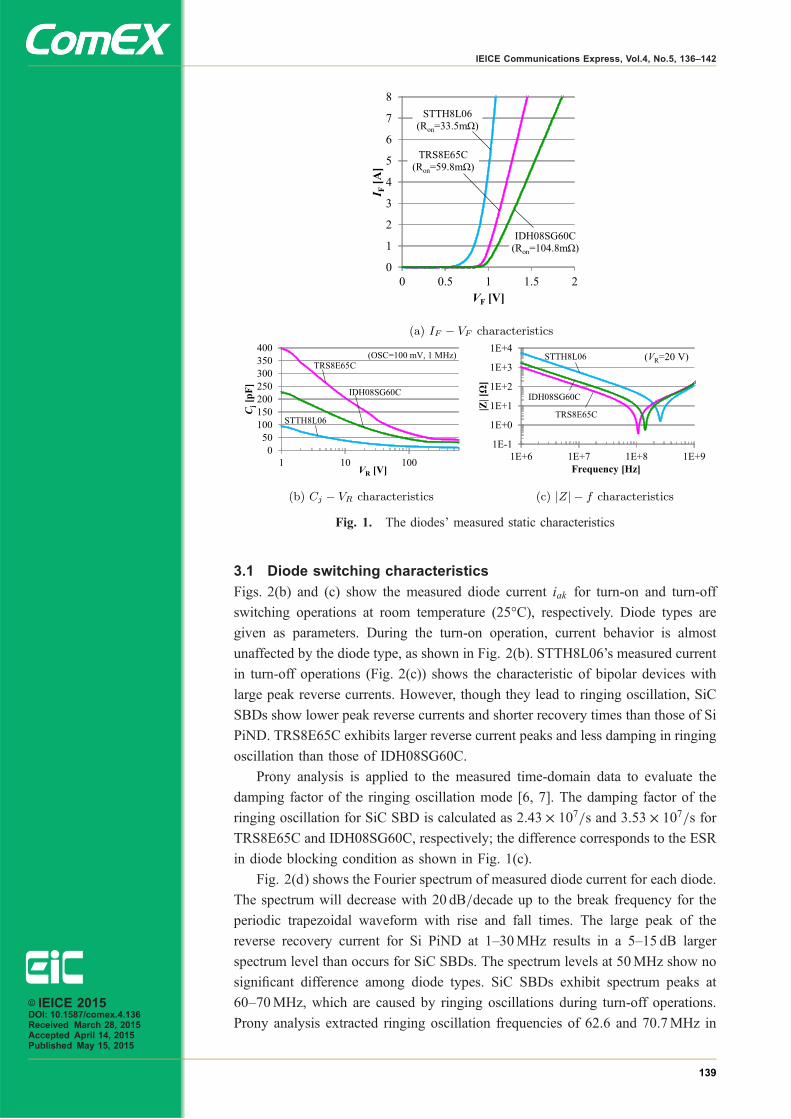
2 Temperature dependence in the static characteristics of diodes
Fig. 1(a) shows the measured forward current–voltage (IF–VF) characteristics of
the studied diodes at room temperature (25 °C) using a curve tracer (Agilent
B1505). Both Si PiND and SiC SBD have knee voltage and their forward
characteristics show almost the same tendency. The two SiC SBDs have almost
the same knee voltage; however, the on-resistance of IDH08SG60C is approxi-
mately 1.7 times larger than that of TRS8E65C.
Fig. 1(b) shows the measured capacitance–voltage (Cj–VR) characteristics of
the studied diodes in a blocking condition with a 100mV, 1MHz AC measurement
signal. The SiC SBDs have larger junction capacitances than Si PiND because of
higher impurity concentrations in the drift region [4]. The capacitance for
TRS8E65C is twice as large as that for IDH08SG60C in the lower reverse bias
voltage range, which corresponds to the difference in on-resistance.
Fig. 1(c) shows the measured frequency characteristics of the studied diodes’
impedance jZj in a blocking condition (VR ¼ 20V) using an impedance analyzer
(Keysight E4991B). All samples’ frequency responses show as RLC series equiv-
alent circuits. The equivalent series inductances are almost identical for the same
TO-220 package. The series resonance frequency of 100–300MHz corresponds
with the diodes’ junction capacitances. STTH8L06 shows a larger equivalent series
resistance (ESR) than that of the SiC SBDs, which are identified from minimum
impedance at the series resonance frequency. IDH08SG60C’s ESR is approxi-
mately 1.3 times larger than that of TRS8E65C.
3 Diode switching characteristics and conducted emissions for the
CCM boost converter
Fig. 2(a) depicts the CCM boost converter’s circuit diagram [5]. The MOSFET
(Infineon, IPP60R099CP) was operated at a 100 kHz switching frequency with
50% duty cycle for a 100V DC input voltage and 75Ω load resistance. Output
voltage was 200V DC. Si PiND induces large reverse recovery currents during
turn-off operations because of stored minority carriers, as shown in Fig. 2(a), which
results in large switching losses and noise in CCM converters. In contrast, SiC SBD
is free from the reverse recovery phenomena because it operates with the majority
carrier; thus, only the depletion charge is observed during turn-off operations.
Hence, SiC SBDs have less switching losses and their lower peak reverse currents
induce less surge voltages. However, their fast switching and small terminal
capacitances could cause high frequency oscillation and noticeable EMI noise in
high-frequency ranges. This section focuses on the turn-off operations of the
studied Si PiND and SiC SBDs and evaluates the switching characteristics of
diode currents during turn-off operations.
© IEICE 2015DOI: 10.1587/comex.4.136Received March 28, 2015Accepted April 14, 2015Published May 15, 2015
138
IEICE Communications Express, Vol.4, No.5, 136–142
3.1 Diode switching characteristics
Figs. 2(b) and (c) show the measured diode current iak for turn-on and turn-off
switching operations at room temperature (25°C), respectively. Diode types are
given as parameters. During the turn-on operation, current behavior is almost
unaffected by the diode type, as shown in Fig. 2(b). STTH8L06’s measured current
in turn-off operations (Fig. 2(c)) shows the characteristic of bipolar devices with
large peak reverse currents. However, though they lead to ringing oscillation, SiC
SBDs show lower peak reverse currents and shorter recovery times than those of Si
PiND. TRS8E65C exhibits larger reverse current peaks and less damping in ringing
oscillation than those of IDH08SG60C.
Prony analysis is applied to the measured time-domain data to evaluate the
damping factor of the ringing oscillation mode [6, 7]. The damping factor of the
ringing oscillation for SiC SBD is calculated as 2:43 � 107/s and 3:53 � 107/s for
TRS8E65C and IDH08SG60C, respectively; the difference corresponds to the ESR
in diode blocking condition as shown in Fig. 1(c).
Fig. 2(d) shows the Fourier spectrum of measured diode current for each diode.
The spectrum will decrease with 20 dB/decade up to the break frequency for the
periodic trapezoidal waveform with rise and fall times. The large peak of the
reverse recovery current for Si PiND at 1–30MHz results in a 5–15 dB larger
spectrum level than occurs for SiC SBDs. The spectrum levels at 50MHz show no
significant difference among diode types. SiC SBDs exhibit spectrum peaks at
60–70MHz, which are caused by ringing oscillations during turn-off operations.
Prony analysis extracted ringing oscillation frequencies of 62.6 and 70.7MHz in
Fig. 1. The diodes’ measured static characteristics
© IEICE 2015DOI: 10.1587/comex.4.136Received March 28, 2015Accepted April 14, 2015Published May 15, 2015
139
IEICE Communications Express, Vol.4, No.5, 136–142
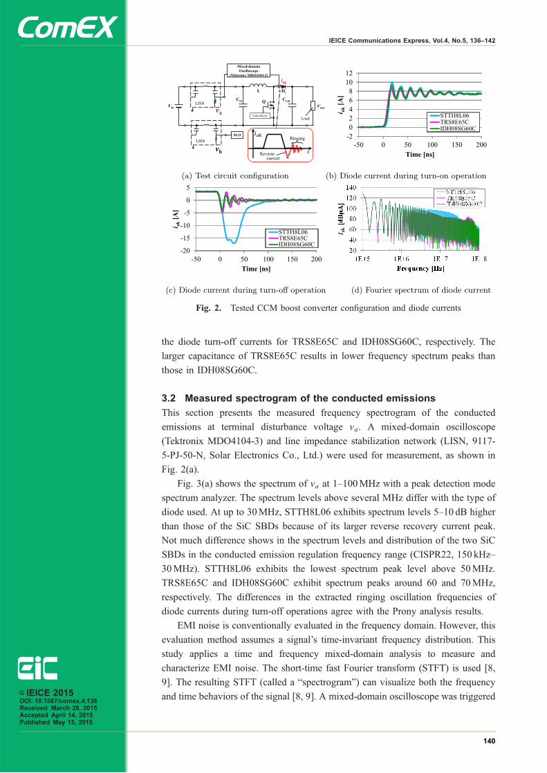
the diode turn-off currents for TRS8E65C and IDH08SG60C, respectively. The
larger capacitance of TRS8E65C results in lower frequency spectrum peaks than
those in IDH08SG60C.
3.2 Measured spectrogram of the conducted emissions
This section presents the measured frequency spectrogram of the conducted
emissions at terminal disturbance voltage va. A mixed-domain oscilloscope
(Tektronix MDO4104-3) and line impedance stabilization network (LISN, 9117-
5-PJ-50-N, Solar Electronics Co., Ltd.) were used for measurement, as shown in
Fig. 2(a).
Fig. 3(a) shows the spectrum of va at 1–100MHz with a peak detection mode
spectrum analyzer. The spectrum levels above several MHz differ with the type of
diode used. At up to 30MHz, STTH8L06 exhibits spectrum levels 5–10 dB higher
than those of the SiC SBDs because of its larger reverse recovery current peak.
Not much difference shows in the spectrum levels and distribution of the two SiC
SBDs in the conducted emission regulation frequency range (CISPR22, 150 kHz–
30MHz). STTH8L06 exhibits the lowest spectrum peak level above 50MHz.
TRS8E65C and IDH08SG60C exhibit spectrum peaks around 60 and 70MHz,
respectively. The differences in the extracted ringing oscillation frequencies of
diode currents during turn-off operations agree with the Prony analysis results.
EMI noise is conventionally evaluated in the frequency domain. However, this
evaluation method assumes a signal’s time-invariant frequency distribution. This
study applies a time and frequency mixed-domain analysis to measure and
characterize EMI noise. The short-time fast Fourier transform (STFT) is used [8,
9]. The resulting STFT (called a “spectrogram”) can visualize both the frequency
and time behaviors of the signal [8, 9]. A mixed-domain oscilloscope was triggered
Fig. 2. Tested CCM boost converter configuration and diode currents
© IEICE 2015DOI: 10.1587/comex.4.136Received March 28, 2015Accepted April 14, 2015Published May 15, 2015
140
IEICE Communications Express, Vol.4, No.5, 136–142
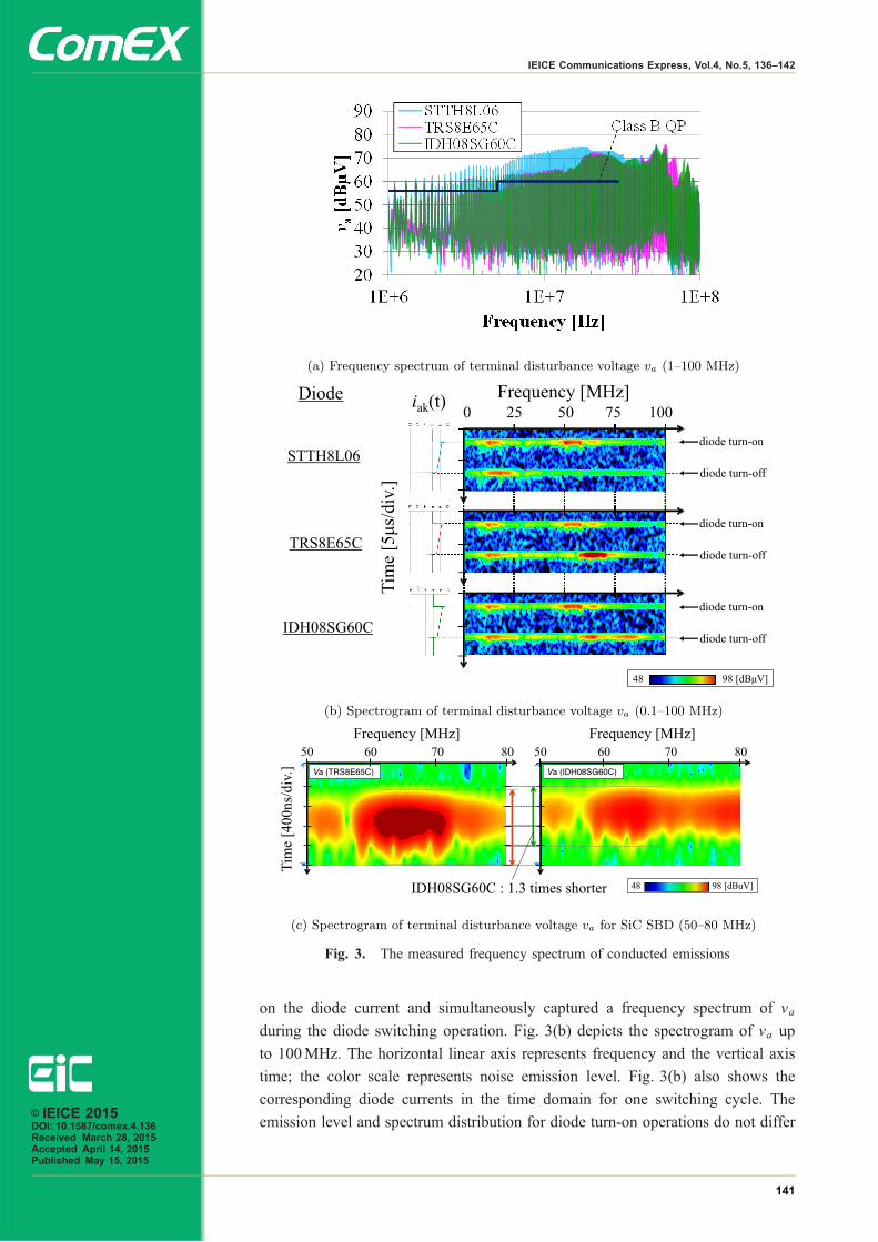
on the diode current and simultaneously captured a frequency spectrum of va
during the diode switching operation. Fig. 3(b) depicts the spectrogram of va up
to 100MHz. The horizontal linear axis represents frequency and the vertical axis
time; the color scale represents noise emission level. Fig. 3(b) also shows the
corresponding diode currents in the time domain for one switching cycle. The
emission level and spectrum distribution for diode turn-on operations do not differ
Fig. 3. The measured frequency spectrum of conducted emissions
© IEICE 2015DOI: 10.1587/comex.4.136Received March 28, 2015Accepted April 14, 2015Published May 15, 2015
141
IEICE Communications Express, Vol.4, No.5, 136–142
with the type of diode. STTH8L06 exhibits the highest spectrum level, stemming
from its larger reverse current peak, at 1–30MHz; it also exhibits the lowest
spectrum levels above 50MHz during diode turn-off operations (Fig. 3(b)). The
ringing oscillations during SiC SBD turn-offs cause conducted emissions at
60–80MHz. Fig. 3(c) is the spectrogram of va for diode turn-off operations
magnified from 50–80MHz. TRS8E65C results in higher levels and less damping
noise spectrums than IDH08SG60C at 60–70MHz. The damping time constant of
the noise spectrum for IDH08SG60C is approximately 1.3 times shorter than that
for TRS8E65C. These differences agree with the extracted ESR shown in Fig. 1(c)
and the extracted damping of ringing oscillations obtained through Prony analysis.
Thus, diode turn-off characteristics have significant influence on the conducted
emissions level and its dynamic behavior in frequency ranges of >50MHz.
4 Conclusion
This study elucidates the static and switching characteristics of diodes that could
affect the conducted emissions of CCM boost converters. Because of their smaller
recovery currents, SiC SBDs give less line-conducted emissions levels at up to
30MHz than does Si PiND. The ringing oscillation of diode currents during turn-
off operations and EMI noise levels at frequency ranges of >50MHz depend on the
ESR and junction capacitance of SiC SBDs. Prony analysis could evaluate the
switching characteristics of diode currents during turn-off operations. The extracted
damping factor and ringing oscillation frequency are in good agreement with the
results of the spectrogram for conducted emissions. The spectrogram demonstrates
the transient characterization of the noise spectrum. Analysis results show that
diode turn-off characteristics influence conducted emissions in CCM DC–DC boost
converters. Thus, the analysis of time and frequency mixed domains can character-
ize both noise sources and EMI noise emissions.
Acknowledgments
This work was partially supported by Grant-in-Aid for Japan Society for the
Promotion of Science (JSPS) Fellows (DC2), and by Council for Science, Tech-
nology and Innovation (CSTI), Cross-ministerial Strategic Innovation Promotion
Program (SIP), “Next-generation power electronics” (funding agency: NEDO).
© IEICE 2015DOI: 10.1587/comex.4.136Received March 28, 2015Accepted April 14, 2015Published May 15, 2015
142
IEICE Communications Express, Vol.4, No.5, 136–142
Configuration of MIMOsystem using single leakycoaxial cable for linear cellenvironments
Yafei Hou1,2a), Satoshi Tsukamoto2, Takahiro Maeda2,Masayuki Ariyoshi2, Kiyoshi Kobayashi2,Tomoaki Kumagai2, and Minoru Okada11 Graduate School of Information Science, Nara Institute of Science and Technology,
8916–5 Takayama, Ikoma, Nara 630–0195, Japan2 ATR Wave Engineering Laboratories,
2–2–2 Hikaridai, Keihanna Science City, Kyoto 619–0288, Japan
Abstract: It has been conventionally assumed that a single leaky coaxial
(LCX) cable only is utilized as one antenna to configure a multiple-input
multiple-output (MIMO) system. In this letter, we show one single LCX
cable can be used as two antennas to configure a MIMO system owing to the
designed intersection angle between the different radiation directivities of
both input signals. The measurement results of 2 × 2 LCX-MIMO channel
quality confirm that our proposed LCX-MIMO can realize a promising
channel condition over 5GHz frequency band. It also points out that the
intersection angle between radiation directivities of LCX cable needs to be
considered carefully to reduce the channel degradation at the both edge
portions of the LCX cable.
Keywords: leaky coaxial cable, multiple-input multiple-output, channel
quality
Classification: Wireless Communication Technologies
References
[1] J. Medbo and A. Nilsson, “Leaky coaxial cable MIMO performance in an indooroffice environment,” Proc. 23th IEEE international Symposium on Personal,Indoor and Mobile Radio Communications (PIMRC2012), Sydney, Australia,pp. 2061–2066, Sept. 2012. DOI:10.1109/PIMRC.2012.6362694
[2] Y. Hou, S. Tsukamoto, M. Okada, et al., “2 by 2 MIMO system using singleleaky coaxial cable for linear-cells,” Proc. 25th IEEE international Symposiumon Personal, Indoor and Mobile Radio Communications (PIMRC 2014),Washington, USA, pp. 408–412, Sept. 2014.
[3] Y. Hou, S. Tsukamoto, M. Ariyoshi, K. Kobayashi, T. Kumagai, and M. Okada,“Performance comparison for 2 by 2 MIMO system using single leaky coaxialcable over WLAN frequency band,” Proc. 25th Asia-Pacific Signal and Informa-tion Processing Association Annual Summit and Conference (APSIPA ASC2014), Siem Reap, Cambodia, pp. 1–6, Dec. 2014. DOI:10.1109/APSIPA.2014.7041735
© IEICE 2015DOI: 10.1587/comex.4.143Received March 26, 2015Accepted April 16, 2015Published May 19, 2015
143
IEICE Communications Express, Vol.4, No.5, 143–148
[4] S. Tsukamoto, T. Maeda, M. Ariyoshi, Y. Hou, K. Kobayashi, and T. Kumagai,“An experimental evaluation of 2 × 2 MIMO system using closely-spacedleaky coaxial cables,” Proc. 25th Asia-Pacific Signal and Information ProcessingAssociation Annual Summit and Conference (APSIPA ASC 2014), Siem Reap,Cambodia, pp. 1–6, Dec. 2014. DOI:10.1109/APSIPA.2014.7041676
[5] Y. Hou, S. Tsukamoto, M. Ariyoshi, K. Kobayashi, and M. Okada, “4-by-4MIMO channel using two leaky coaxial cables (LCXs) for wireless applicationsover linear-cell,” Proc. 3rd IEEE Global Conference on Consumer Electronics(GCCE 2014), Tokyo, Japan, pp. 125–126, Oct. 2014. DOI:10.1109/GCCE.2014.7031177
[6] Y. Hou, S. Tsukamoto, M. Okada, et al., “Realization of 4-by-4 MIMO channelusing one composite leaky coaxial cable,” Proc. 12th Annual IEEE ConsumerCommunications and Networking Conference (CCNC 2015), Las Vegas, USA,pp. 103–108, Jan. 2015.
[7] J. W. Huang and K. K. Mei, “Theory and analysis of leaky coaxial cables withperiodic slots,” IEEE Trans. Antennas Propag., vol. 49, no. 12, pp. 1723–1732,Dec. 2001. DOI:10.1109/8.982452
1 Introduction
One of the hottest topics among the global telecoms industry is of how to improve
the spectrum efficiency for specific wireless network scenarios. There are many
scenarios known as linear-cell environments where the wireless transmission is
operated over a long and shallow place such as tunnels, along railways, under-
ground shopping malls, and so on. For these environments, a wireless system using
leaky coaxial (LCX) cable as an antenna for radio communication is widely used
because LCX has many potential advantages compared with conventional Omni-
directional antenna. For example, its coverage is uniform and the antenna place-
ments to deduce an interference might be simpler. In addition, the handover process
of conventional cells can be avoided when users are moving.
Recently thin LCX has been developed to be utilized for higher frequency
such as 2.4GHz band, 5GHz band for WLAN systems. To improve the spectral
efficiency of WLAN system over linear-cell environments, LCX cable can be
utilized as antenna to configure the multiple-input multiple-output (MIMO) chan-
nel. In paper [1], two independent LCX cables were applied to configure a 2 � 2
indoor MIMO system for corridor scenario and office landscape scenario, which
can realize an channel quality close to an independent and identically distributed
(i:i:d:) one. However, utill now, these researches have assumed that one LCX cable
is singlely treated as one antenna. Therefore it needs more than one LCX cable
to configure an MIMO system. This requires more cost for configuration of
MIMO, and large spacing between LCX cables is also necessary to reduce channel
correlation.
We have recently proposed a method that one single LCX cable can be used as
two antennas [2, 3, 4, 5, 6]. When different RF transmit signals are fed to each end
of the cable, the single LCX can work as two antennas. The results in [2] confirm
that, over 2.4GHz frequency band, the proposed MIMO channel using a single
LCX cable can realize good 2 � 2 channel condition even within a highly correlated© IEICE 2015DOI: 10.1587/comex.4.143Received March 26, 2015Accepted April 16, 2015Published May 19, 2015
144
IEICE Communications Express, Vol.4, No.5, 143–148
propagation condition. The 2 � 2 MIMO performance comparison between that
using the LCX cable and using Omni-direction antenna has been reported with
simulated results in [3] and with experimental evaluation in [4]. It also showed that
by adjusting the period of slot, we can use one composite cable, which consists of a
pair of LCX cables with different radiation directivities, to configure a 4 � 4MIMO
channel. The measurement results using the proposed LCXs over 5GHz band
confirm that the proposed composite LCX cable can realize a good MIMO channel
condition even if the spacing between the pair of LCXs is just 2 cm [5, 6].
Therefore the proposed LCX cable can reduce the space requirement for MIMO
deployment over linear-cell environments.
In this letter, we show the measurement results about the 2 � 2 MIMO channel
quality using single LCX with different radiation directivities over 5GHz frequency
band. The results confirm that our proposed LCX-MIMO can realize better channel
quality than the i:i:d: channel. It also shows that the intersection angle between
dominant radiation directivities of the LCX cable needs to be designed carefully to
reduce the channel degradation at the both edge portions of LCX cable.
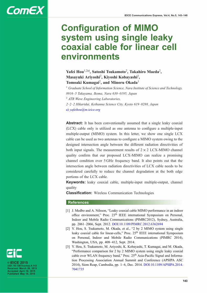
2 LCX cable and its propagation direction
Fig. 1(a) shows an example of LCX cable structure. Radio wave is radiated and
received from slots which are periodically located along the outer conductor in the
cable. Signal strength of radio waves at the far field region from LCX is related to
the sum of the radiated radio waves from the slots. Radiation angles with peak
directivity are
�m ¼ sin�1ffiffiffiffi�r
p þ m�RFP
� �; ðm ¼ �1;�2; . . .Þ ð1Þ
where m is an order of harmonic, �r is relative permittivity of insulator in LCX, �RFis the wavelength of input radio frequency (RF) signal, and P is the period of slots
[7]. �m are propagation angles. To avoid radiation of harmonics, LCX is typically
Fig. 1. LCX cable structure and its propagation direction
© IEICE 2015DOI: 10.1587/comex.4.143Received March 26, 2015Accepted April 16, 2015Published May 19, 2015
145
IEICE Communications Express, Vol.4, No.5, 143–148
designed as taking value m ¼ �1. By changing the period of slot P, the dominant
propagation angle of LCX ��1 is accordingly changed. Therefore, we can design
��1 as any nonzero value. As an example shown in Fig. 1(b), the dominant
propagation angles of two different input RF signal propagations from port 1
and 2 can have an intersection angle as 2��1. We can use this property to adjust the
value 2��1 to achieve a promising MIMO channel condition.
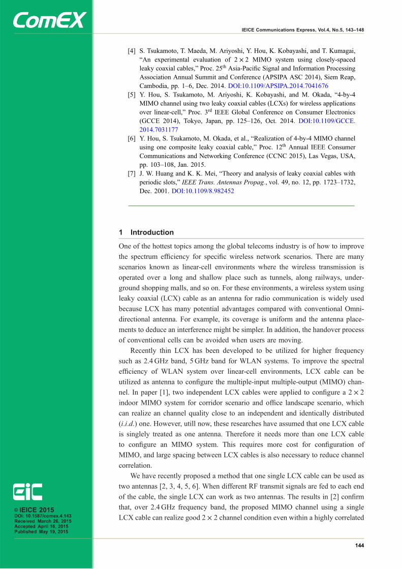
3 Proposed 2-by-2 LCX-MIMO system
3.1 Proposed 2-by-2 LCX-MIMO structure
On the basis of the previous explanation, we designed a 2 � 2 LCX MIMO system
using single LCX cable as shown in Fig. 2. Here station (STA) has two conven-
tional antennas. Since the LCX have dominant wave directions that is not 0 degree,
the access point (AP) exploits the MIMO technique using both ends of LCX cable
as the antenna inputs shown as port 1 and 2. Two different radiation wave
directivities are shown in the figure as A and B. The signal at one receiving
antenna can have low correlation compared with that at the other. If two receiving
antennas have appropriate spacing and keep an appropriate distance from center of
the LCX, two-stream MIMO can be achieved.
3.2 Measurement parameters
For the confirmation of the proposed LCX-MIMO performance over 5GHz
frequency band, 2 � 2 LCX-MIMO channel matrices between the LCX cable
and two receiving antennas were measured using a multi-ports vector network
analyzer in an anechoic chamber. The configuration of the measurement is also
shown with measurement points within the area in Fig. 2. Here X axis is the
direction along the LCX cable and Yaxis is the direction from the LCX cable to the
receiving antenna. An origin point is defined at the center of the LCX cable of 10
meters length. Each receiving antenna has omnidirectional radiation pattern. The
separation between the two receiving antennas is one wavelength or 6mm. Since
there are reduced reflection paths and the channel propagation is static in an
anechoic chamber, a shape of a cell that is formed by the LCX is assumed to be
symmetric against X axis and Y axis. We measure the channel with the equal
spacing of 25.4mm when STA is moving along X axis from 0 meter to 5 meter
which has 200 positions for each fixed Y.
Fig. 2. 2-by-2 MIMO system with proposed LCX cable
© IEICE 2015DOI: 10.1587/comex.4.143Received March 26, 2015Accepted April 16, 2015Published May 19, 2015
146
IEICE Communications Express, Vol.4, No.5, 143–148
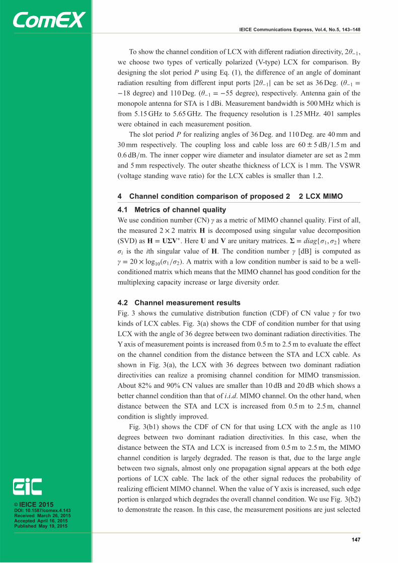
To show the channel condition of LCX with different radiation directivity, 2��1,we choose two types of vertically polarized (V-type) LCX for comparison. By
designing the slot period P using Eq. (1), the difference of an angle of dominant
radiation resulting from different input ports j2��1j can be set as 36Deg. (��1 ¼�18 degree) and 110Deg. (��1 ¼ �55 degree), respectively. Antenna gain of the
monopole antenna for STA is 1 dBi. Measurement bandwidth is 500MHz which is
from 5.15GHz to 5.65GHz. The frequency resolution is 1.25MHz. 401 samples
were obtained in each measurement position.
The slot period P for realizing angles of 36Deg. and 110Deg. are 40mm and
30mm respectively. The coupling loss and cable loss are 60 � 5 dB/1.5m and
0.6 dB/m. The inner copper wire diameter and insulator diameter are set as 2mm
and 5mm respectively. The outer sheathe thickness of LCX is 1mm. The VSWR
(voltage standing wave ratio) for the LCX cables is smaller than 1.2.
4 Channel condition comparison of proposed 2� 2 LCX MIMO
4.1 Metrics of channel quality
We use condition number (CN) γ as a metric of MIMO channel quality. First of all,
the measured 2 � 2 matrix H is decomposed using singular value decomposition
(SVD) as H ¼ U�V�. Here U and V are unitary matrices. � ¼ diagf�1; �2g where
�i is the ith singular value of H. The condition number γ [dB] is computed as
� ¼ 20 � log10ð�1=�2Þ. A matrix with a low condition number is said to be a well-
conditioned matrix which means that the MIMO channel has good condition for the
multiplexing capacity increase or large diversity order.
4.2 Channel measurement results
Fig. 3 shows the cumulative distribution function (CDF) of CN value γ for two
kinds of LCX cables. Fig. 3(a) shows the CDF of condition number for that using
LCX with the angle of 36 degree between two dominant radiation directivities. The
Y axis of measurement points is increased from 0.5m to 2.5m to evaluate the effect
on the channel condition from the distance between the STA and LCX cable. As
shown in Fig. 3(a), the LCX with 36 degrees between two dominant radiation
directivities can realize a promising channel condition for MIMO transmission.
About 82% and 90% CN values are smaller than 10 dB and 20 dB which shows a
better channel condition than that of i:i:d: MIMO channel. On the other hand, when
distance between the STA and LCX is increased from 0.5m to 2.5m, channel
condition is slightly improved.
Fig. 3(b1) shows the CDF of CN for that using LCX with the angle as 110
degrees between two dominant radiation directivities. In this case, when the
distance between the STA and LCX is increased from 0.5m to 2.5m, the MIMO
channel condition is largely degraded. The reason is that, due to the large angle
between two signals, almost only one propagation signal appears at the both edge
portions of LCX cable. The lack of the other signal reduces the probability of
realizing efficient MIMO channel. When the value of Y axis is increased, such edge
portion is enlarged which degrades the overall channel condition. We use Fig. 3(b2)
to demonstrate the reason. In this case, the measurement positions are just selected© IEICE 2015DOI: 10.1587/comex.4.143Received March 26, 2015Accepted April 16, 2015Published May 19, 2015
147
IEICE Communications Express, Vol.4, No.5, 143–148
from 0 to 2m. We find that the proposed LCX-MIMO can achieve a better channel
condition than that of i:i:d: MIMO channel. Therefore it needs to be considered
how to improve the MIMO channel condition of the LCX edge area by selecting an
appropriate ��1.
5 Conclusions
This letter has showed the measurement results about the 2 � 2 MIMO channel
quality using a single LCX with different radiation directivities over 5GHz
frequency band. The results confirm that the proposed LCX-MIMO can realize a
better channel condition than that of the i:i:d channel. It also showed that its
coverage area needs to be considered carefully to reduce the channel condition
degradation at the both edge portions of LCX cable.
Acknowledgments
This work is supported by the Ministry of Internal Affairs and Communications
SCOPE (Strategic Information and Communications R&D Promotion Programme)
2014 with grant number as 135007001.
Fig. 3. CDF of condition number of 2 � 2 LCX-MIMO
© IEICE 2015DOI: 10.1587/comex.4.143Received March 26, 2015Accepted April 16, 2015Published May 19, 2015
148
IEICE Communications Express, Vol.4, No.5, 143–148
Path loss model for the 2to 37GHz band in streetmicrocell environments
Minoru Inomata1a), Wataru Yamada1, Motoharu Sasaki1,Masato Mizoguchi1, Koshiro Kitao2, and Tetsuro Imai21 NTT Access Network Service Systems Laboratories, NTT Corporation,
1–1 Hikarinooka, Yokosuka, Kanagawa 239–0847, Japan2 NTT DOCOMO, INC., 3–6 Hikarino-oka, Yokosuka, Kanagawa 239–8536, Japan
Abstract: A path loss model based on the Rec. ITU-R P.1411 model, which
can cover the frequency range from microwave to millimeter-wave bands, is
presented. The path loss characteristics are analyzed on the basis of measure-
ment results obtained using the 2 to 37GHz band in street microcell
environments. It is clarified that the characteristics depend on distance from
transmitter to intersection and frequency dependency. By taking these
dependencies into account, the proposed model can decrease the root mean
square error of prediction results to within about 5 dB in the 2 to 37GHz
band.
Keywords: propagation, millimeter wave, street microcell environment
Classification: Antennas and Propagation
References
[1] NTT DOCOMO, INC., “DOCOMO 5G White Paper, 5G Radio Access:Requirements, Concept and Technologies”, July 2014.
[2] METIS, https://www.metis2020.com/.[3] Rep. ITU-R M.2135-1, “Guidelines for evaluation of radio interface technol-
ogies for IMT-Advanced,” ITU-R Report, vol. 1, M Series, ITU, Geneva, 2009.[4] Rec. ITU-R P.1411-7, “Propagation data and prediction methods for the
planning of short-range outdoor radiocommunication systems and radio localarea networks in the frequency range 300MHz to 100GHz,” ITU-R Report,vol. 7, P Series, ITU, Geneva, 2013.
[5] X. Zhao, T. Rautiainen, K. Kalliola, and P. Vainikainen, “Path-loss models forurban microcells at 5.3GHz,” IEEE Antennas Wireless Propag. Lett., vol. 5,pp. 152–154, Dec. 2006. DOI:10.1109/LAWP.2006.873950
[6] K. Sakawa, H. Masui, M. Ishii, H. Shimizu, and T. Kobayashi, “Microwavepath-loss characteristics in an urban area with base station antenna on top of atall building,” International Zurich Seminar on Broadband Communications,pp. 31-1–31-4, 2002. DOI:10.1109/IZSBC.2002.991774
© IEICE 2015DOI: 10.1587/comex.4.149Received March 31, 2015Accepted April 14, 2015Published May 19, 2015
149
IEICE Communications Express, Vol.4, No.5, 149–154
1 Introduction
Traffic in wireless communication systems has been rapidly increasing in recent
years and is assumed to reach 1000 times higher than the current traffic amount in
the next 10 years [1]. To cope with this growth, the application of both microwave
and millimeter-wave bands for the next generation mobile systems is being
examined since millimeter-wave bands can use wider frequency bandwidth that
can provide attractive higher throughput.
It is assumed that one of the possible service areas of mobile systems using
millimeter-wave bands is urban downtown areas, well known as street microcell
environments [2]. A lot of path loss models for street microcell environments have
been proposed; most of them can be categorized into two types. The first type is
two-slope models, of which the Rep. ITU-R M.2135 model [3] is the representative
example. However, the applicable frequency range of this model is only from 2 to
6GHz. The other is three-slope models, of which the Rec. ITU-R P.1411 model [4]
is the representative example. The applicable frequency range of this model is from
2 to 16GHz. However, no models covering millimeter-wave bands have yet been
reported.
A single path loss model that can cover the frequency range from microwave to
millimeter-wave bands is preferable in terms of measuring the consistency of
frequency characteristics, though to the authors’ knowledge no such models have
been reported. To address this deficiency, we propose a model that is based on the
Rec. ITU-R P.1411 model and can cover the frequency range from microwave to
millimeter-wave bands. Since the P.1411 model is constructed with parameters it
can extend the frequency range so as to cover bands from microwave to millimeter-
wave. However, since each of the coefficients of Rep. ITU-R M.2135 model are
optimized in the target frequency range, it will be necessary to reconstruct the
coefficients to extend the frequency range [5, 6].
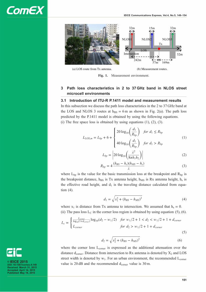
2 Measurement parameters and environments
The path loss measurements were taken in the environment shown in Fig. 1(a). The
measurements were taken in four frequency bands 2, 4.7, 26, and 37GHz in order
to ascertain the frequency dependence of the measurements. The transmitter (Tx)
antenna was set to a height of either 6 or 10m and used to transmit continuous
waves. A receiver (Rx) antenna was fixed on the roof of a measurement car whose
height was 2.5m. The antenna directivity was omni-directional. The received
power level was measured while driving the measurement car along the line-of-
sight (LOS), non-line-of-sight (NLOS) 1, NLOS 2, and NLOS 3 routes as shown
in Fig. 1(b). The measurement procedure was conducted in Tokyo, Japan. The
distance from Tx antenna to intersection was about 242m for NLOS 1, 57m for
NLOS 2, and 169m for NLOS 3. Tall buildings of about ten stories about 40m
height surrounded the street in the measurement site.
© IEICE 2015DOI: 10.1587/comex.4.149Received March 31, 2015Accepted April 14, 2015Published May 19, 2015
150
IEICE Communications Express, Vol.4, No.5, 149–154
3 Path loss characteristics in 2 to 37GHz band in NLOS street
microcell environments
3.1 Introduction of ITU-R P.1411 model and measurement results
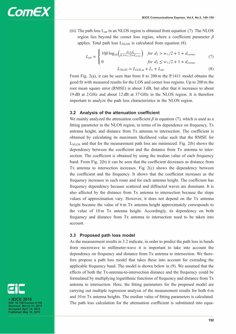
In this subsection we discuss the path loss characteristics in the 2 to 37GHz band at
the LOS and NLOS 3 routes at hBS ¼ 6m as shown in Fig. 2(a). The path loss
predicted by the P.1411 model is obtained by using the following equations.
(i) The free space loss is obtained by using equations (1), (2), (3).
LLOS;m ¼ Lbp þ 6 þ20 log10
d1Rbp
� �for d1 � Rbp
40 log10d1Rbp
� �for d1 > Rbp
8>>><>>>:
ð1Þ
Lbp ¼ 20 log10�2
8�h1h2
� ��������� ð2Þ
Rbp ¼ 4ðhBS � hsÞðhMS � hsÞ
�ð3Þ
where Lbp is the value for the basic transmission loss at the breakpoint and Rbp is
the breakpoint distance, hBS is Tx antenna height, hMS is Rx antenna height, hs is
the effective road height, and d1 is the traveling distance calculated from equa-
tion (4).
d1 ¼ffiffiffiffiffiffiffiffiffiffiffiffiffiffiffiffiffiffiffiffiffiffiffiffiffiffiffiffiffiffiffiffiffiffiffix21 þ ðhBS � hMSÞ2
qð4Þ
where x1 is distance from Tx antenna to intersection. We assumed that hs ¼ 0.
(ii) The pass loss LC in the corner loss region is obtained by using equation (5), (6).
Lc ¼Lcorner
log10ð1þdcornerÞ log10ðd2 � w1=2Þ for w1=2 þ 1 < d2 < w1=2 þ 1 þ dcorner
Lcorner for d2 > w1=2 þ 1 þ dcorner
(
ð5Þd2 ¼
ffiffiffiffiffiffiffiffiffiffiffiffiffiffiffiffiffiffiffiffiffiffiffiffiffiffiffiffiffiffiffiffiffiffiffix22 þ ðhBS � hMSÞ2
qð6Þ
where the corner loss Lcorner is expressed as the additional attenuation over the
distance dcorner. Distance from intersection to Rx antenna is denoted by X2 and LOS
street width is denoted by w1. For an urban environment, the recommended Lcorner
value is 20 dB and the recommended dcorner value is 30m.
(a) LOS route from Tx antenna. (b) Measurement routes.
Fig. 1. Measurement environment.
© IEICE 2015DOI: 10.1587/comex.4.149Received March 31, 2015Accepted April 14, 2015Published May 19, 2015
151
IEICE Communications Express, Vol.4, No.5, 149–154
(iii) The path loss Latt in an NLOS region is obtained from equation (7). The NLOS
region lies beyond the corner loss region, where a coefficient parameter β
applies. Total path loss LNLOS is calculated from equation (8).
Latt ¼10� log10
d1þd2d1þw1=2þdcorner
� �for d2 > w1=2 þ 1 þ dcorner
0 for d2 � w1=2 þ 1 þ dcorner
8<: ð7Þ
LNLOS ¼ LLOS;m þ Lc þ Latt ð8ÞFrom Fig. 2(a), it can be seen that from 0 to 200m the P.1411 model obtains the
good fit with measured results for the LOS and corner loss regions. Up to 200m the
root mean square error (RMSE) is about 3 dB, but after that it increases to about
19 dB at 2GHz and about 12 dB at 37GHz in the NLOS region. It is therefore
important to analyze the path loss characteristics in the NLOS region.
3.2 Analysis of the attenuation coefficient
We mainly analyzed the attenuation coefficient β in equation (7), which is used as a
fitting parameter in the NLOS region, in terms of its dependence on frequency, Tx
antenna height, and distance from Tx antenna to intersection. The coefficient is
obtained by calculating its maximum likelihood value such that the RMSE for
LNLOS and that for the measurement path loss are minimized. Fig. 2(b) shows the
dependency between the coefficient and the distance from Tx antenna to inter-
section. The coefficient is obtained by using the median value of each frequency
band. From Fig. 2(b) it can be seen that the coefficient decreases as distance from
Tx antenna to intersection increases. Fig. 2(c) shows the dependency between
the coefficient and the frequency. It shows that the coefficient increases as the
frequency increases in each route and for each antenna height. The coefficient has
frequency dependency because scattered and diffracted waves are dominant. It is
also affected by the distance from Tx antenna to intersection because the slope
values of approximation vary. However, it does not depend on the Tx antenna
height because the value of 6m Tx antenna height approximately corresponds to
the value of 10m Tx antenna height. Accordingly, its dependency on both
frequency and distance from Tx antenna to intersection need to be taken into
account.
3.3 Proposed path loss model
As the measurement results in 3.2 indicate, in order to predict the path loss in bands
from microwave to millimeter-wave it is important to take into account the
dependency on frequency and distance from Tx antenna to intersection. We there-
fore propose a path loss model that takes these into account for extending the
applicable frequency band. The model is shown below in (9). We assumed that the
effects of both the Tx-antenna-to-intersection distance and the frequency could be
formulated by multiplying logarithmic functions of frequency and distance from Tx
antenna to intersection. Here, the fitting parameters for the proposed model are
carrying out multiple regression analysis of the measurement results for both 6m
and 10m Tx antenna heights. The median value of fitting parameters is calculated.
The path loss calculation for the attenuation coefficient is substituted into equa-© IEICE 2015DOI: 10.1587/comex.4.149Received March 31, 2015Accepted April 14, 2015Published May 19, 2015
152
IEICE Communications Express, Vol.4, No.5, 149–154
tion (9). The fitting parameters are calculated for �const ¼ 4:15, �f ¼ 1:41, Cf ¼�7:82, �x ¼ 0:79, and Cx ¼ �1:00. The unit of frequency is MHz and unit of
distance is m.
� ¼ �const þ ð�f log10 f þ CfÞð�x log10 x1 þ CxÞ ð9Þ
(a) Comparison of measurement and prediction results with P.1411 model.
(b) Dependency on distance from Tx to intersection.
(c) Frequency dependency.
Fig. 2. Measurement results.
© IEICE 2015DOI: 10.1587/comex.4.149Received March 31, 2015Accepted April 14, 2015Published May 19, 2015
153
IEICE Communications Express, Vol.4, No.5, 149–154
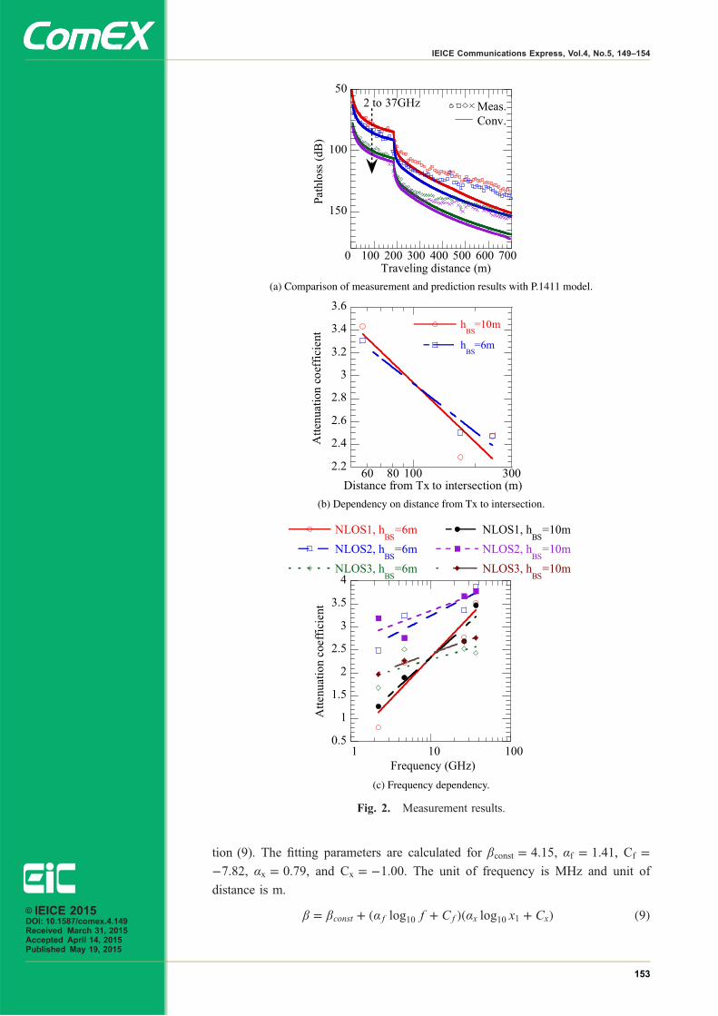
3.4 Verifying validity of proposed path loss model
Fig. 3(a) shows path loss measurement results, prediction results obtained with the
P.1411 model, and prediction results obtained with the proposed model for the LOS
and NLOS 3 routes at hBS ¼ 6m. Quantitative evaluation results are depicted in
Fig. 3(b), where RMSE values for each frequency band are calculated. Black dots
indicate NLOS 1 with hBS ¼ 6m, blue dots NLOS2 with hBS ¼ 6m, green dots
NLOS 3 with hBS ¼ 6m, red dots NLOS 1 with hBS ¼ 10m, purple dots NLOS 2
with hBS ¼ 10m, and brown dots NLOS 3 with hBS ¼ 10m. From Fig. 3(a) it can
be seen that better fitting between predicted and measured values is obtained with
the proposed model than with the P.1411 model, with the former reducing the mean
RMSE value to about 11 dB. Fig. 3(b) shows that with the P.1411 model the RMSE
values were about 6.6 dB at 37GHz and 23.9 dB at 2GHz. The values decrease as
the frequency increases because the recommended attenuation coefficient value is
six, which is a large value to apply to the high frequency band. Fig. 3(b) shows that
with the proposed model the RMSE values are about 2.2 dB at 2GHz and 4.7 dB at
37GHz. This shows that the proposed model can cover the frequency range from 2
to 37GHz.
4 Conclusion
We analyzed path loss characteristics in the 2 to 37GHz band in street microcell
environments with the aim of developing a path loss model that can cover the
frequency range from microwave to millimeter-wave bands. The measurement
results clarified that path loss depends on distance from Tx antenna to intersection
and on frequency. We proposed a frequency extension model that takes account of
these dependencies and confirmed its validity by evaluating the RMSE values of
prediction results obtained with it. The evaluations confirmed it can predict path
loss with RMSE of less than 5 dB in the 2 to 37GHz band.
(a) Path loss in the 2 to 37 GHz band. (b) RMSE in the 2 to 37 GHz band.
Fig. 3. Comparison of proposed and conventional model results.
© IEICE 2015DOI: 10.1587/comex.4.149Received March 31, 2015Accepted April 14, 2015Published May 19, 2015
154
IEICE Communications Express, Vol.4, No.5, 149–154
Performance improvement ofZF-precoded MU-MIMOtransmission by collaborativeinterference cancellation
Hidekazu Murataa) and Ryo ShinoharaGraduate School of Informatics, Kyoto University,
Yoshida-hommachi, Sakyo-ku, Kyoto 606–8501, Japan
Abstract: Multi-user multiple-input and multiple-output (MU-MIMO)
transmission has been extensively studied to enhance the spectral efficiency
of wireless communication systems. The performance of MU-MIMO suffers
due to the presence of residual multi-user interference. Linear interference
cancellation can offer excellent performance when a large number of
antennas are available. This, however, is impractical in a mobile station. In
this paper, we apply a collaborative interference cancellation scheme to a
precoded MU-MIMO system. In order to effect collaboration, we implement
received signal sharing among mobile stations using wireless local area
network connections. We carried out transmission experiments in an indoor
environment to test the performance of our precoded MU-MIMO system
with collaborative interference cancellation.
Keywords: multi-user MIMO, user cooperation, collaborative MIMO,
transmission experiment, interference canceller
Classification: Wireless Communication Technologies
References
[1] H. Murata, “Collaborative interference cancellation for multi-user MIMOcommunication systems,” IEICE Technical Report, RCS2013-201, pp. 159–164,Nov. 2013 (in Japanese).
[2] H. Murata, “Collaborative interference cancellation for future wirelesscommunications,” Proc. 2015 Vietnam–Japan International Symposium onAntennas and Propagation, Ho Chi Minh City, Vietnam, pp. 35–38, Jan. 2015.
[3] H. Kwon and J. M. Cioffi, “Multi-user MISO broadcast channel with user-cooperating decoder,” Proc. IEEE Vehicular Technology Conference, Sept.2008. DOI:10.1109/VETECF.2008.335
[4] J. Lee, S. Kim, H. Suman, T. Kwon, Y. Choi, J. Shin, and A. Park, “Downlink nodecooperation with node selection diversity,” Proc. IEEE Vehicular TechnologyConference, pp. 1494–1498, May 2005. DOI:10.1109/VETECS.2005.1543568
[5] M. Taniguchi, H. Murata, S. Yoshida, K. Yamamoto, D. Umehara, S. Denno,and M. Morikura, “Indoor experiment of multi-user MIMO user selection algo-rithm based on chordal distance,” Proc. Global Telecommunications Conference(GLOBECOM2013), Atlanta, GA, USA, Dec. 2013. DOI:10.1109/GLOCOM.2013.6831692
© IEICE 2015DOI: 10.1587/comex.4.155Received March 31, 2015Accepted April 16, 2015Published May 19, 2015
155
IEICE Communications Express, Vol.4, No.5, 155–160
1 Introduction
Multi-user multiple-input and multiple-output (MU-MIMO) transmission has been
extensively studied in order to improve the spectral efficiency of wireless commu-
nication systems. However, precoding techniques are inherently sensitive to chan-
nel variations. In other words, the performance of MU-MIMO is significantly
affected by the presence of residual multi-user interference. It is well-known that a
linear interference cancellation scheme with a large number of receive antennas can
offer satisfactory performance with reasonable computational complexity. How-
ever, it is impractical to expect such a number of antennas in mobile stations due to
size limitations.
In this paper, we apply collaborative interference cancellation (CIC) [1, 2] to a
precoded MU-MIMO system and test its performance through an experiment. We
employ received signal sharing among mobile stations [3, 4] in the proposed
scheme in order to enhance its interference cancellation capability. We conducted
transmission experiments using wireless local area network (LAN) links for
collaboration in an indoor environment in order to test the performance of our
collaborative interference cancellation scheme implemented on a MU-MIMO
testbed.
2 System model
2.1 Precoding
Consider downlink communication in a MU-MIMO system. For the sake of
simplicity, let us consider a single-carrier frequency in a single-coverage environ-
ment. The base station (BS) equipped with K antennas is serving M mobile stations
(MSs), each with a single antenna. We introduce a linear zero-forcing (ZF) precoder
by exploiting the downlink channel state information (CSI). The transmitted signal
to each MS is collected in the vector s 2 CM�1. In the context of our study, the
received signal of the MSs can be expressed as
y ¼ HWs þ n ¼ s þ n: ð1Þwhere H 2 C
M�K is a channel matrix and n 2 CM�1 is an additive white Gaussian
noise vector. The precoding matrix W 2 CK�M is given by
W ¼ Hy ¼ HHðHHHÞ�1: ð2ÞIf there exist channel variations �H 2 C
M�K , the off-diagonal elements of
ðI þ �HWÞ cause multi-user interference.
y ¼ ðH þ �HÞWs þ n ¼ ðI þ �HWÞs þ n ð3Þ
2.2 User selection algorithm
In order for the linear precoder to suppress interference, we need to select MSs (also
referred to as users) to serve simultaneously. The number of users cannot be greater
than the number of BS antennas. As a low-complexity user selection method
exploiting the CSI, we introduce the chordal distance-based user selection (CDUS)
algorithm [5].© IEICE 2015DOI: 10.1587/comex.4.155Received March 31, 2015Accepted April 16, 2015Published May 19, 2015
156
IEICE Communications Express, Vol.4, No.5, 155–160
The chordal distance is given by
dcdðHcand;HselÞ ¼ffiffiffiffiffiffiffiffiffiffiffiffiffiffiffiffiffiffiffiffiXJj¼1
sin2 �j
vuut
¼ffiffiffiffiffiffiffiffiffiffiffiffiffiffiffiffiffiffiffiffiffiffiffiffiffiffiffiffiffiffiffiffiffiffiffiffiffiffiffiffiffiffiffiffiffiffiffiffiffiffiffiJ � trð ~Hcand
~HHsel
~Hsel~HHcandÞ
qð4Þ
where Hcand 2 CJ�K is the downlink CSIs of candidate users, Hsel 2 C
NselectedJ�K is
the downlink CSIs of the selected users, �j is the principal angle between the two
subspaces spanned by row j of Hcand and the rows of Hsel, Nselected is the number of
selected users, J is the number of receive antennas of MS, ~½�� represents the Gram–
Schmidt orthonormalization of the rows.
Therefore, by selecting users with greater channel chordal distance among one
another, we can bring the channels of the selected users closer to the orthogonal,
hence improving the performance of linear precoding.
2.3 Collaborative interference cancellation
In order to suppress residual multi-user interference, we apply a collaborative
interference cancellation scheme by utilizing the short-range wireless interface of a
mobile station. In this paper, we employed a simple minimum mean squared error
(MMSE) weight WMMSE 2 CM�M. The weight is given by
WMMSE ¼ ðHWÞHRyy�1
¼ ðHWÞHðHWWHHH þ �Þ�1; ð5Þwhere Ryy 2 C
M�M and � 2 CM�M are autocorrelation matrices of the received
signals and the noise, respectively.
3 Transmission experiments
3.1 Equipment
The testbed used in this research consisted of a BS with four antennas (K ¼ 4) and
six MSs, both implemented using software-defined radio features. We employed
amplify-and-forward (AF) based channel estimation, CDUS, and linear spatial
precoding [5]. The major parameters of the experiment are shown in Table I.
The BS consisted of two instrument chassis and a radio frequency (RF) front
end that included RF amplifiers and RF switches. Power amplifiers (output power at
1 dB compression P1dB ¼ 34:6 dBm, typical) and low-noise amplifiers (noise figure
1.9 dB, typical) were connected to signal generators (SGs) and signal analyzers,
respectively. RF switches were used for duplexing. The control signals of the RF
switches were generated by a field-programmable gate array (FPGA). The trigger
signal was sent from an SG to the FPGA in order to synchronize the transmission
timing of the SGs with the control signals of the RF switches.
A universal software radio peripheral (USRP) was used as a mobile station. We
connected a general-purpose PC to a USRP N210, and carried out baseband signal
processing on the host PC. The motherboard of USRP N210 was equipped with 14-
bit analog-to-digital converters, 16-bit digital-to-analog converters, and an FPGA.
Digital signal processing, such as frequency translation, decimation, and interpo-
lation, was performed on the FPGA.
© IEICE 2015DOI: 10.1587/comex.4.155Received March 31, 2015Accepted April 16, 2015Published May 19, 2015
157
IEICE Communications Express, Vol.4, No.5, 155–160
3.2 Signaling format
A transmission frame was composed of three time slots. The BS first transmitted the
training sequences (TS1s) for round-trip channel estimation at time t ¼ 0. The TS1s
from the BS were orthogonal sequences, and were transmitted at the same time and
frequency. Each MS sent back the received round-trip TS1 using amplify-and-
forward relaying along with another training sequence (TS2) for uplink estimation
at t ¼ 2ms. The BS estimated the downlink channel using the two TSs, and then
transmitted the precoded data packet at t ¼ 10ms. The data packet consisted of the
synchronization word (SW) used for timing synchronization, the training sequence
(TS3) used for demodulation, the control signal used for measurement automation,
and the data sequence along with its cyclic redundancy check.
We established timing synchronization using the SW, which was transmitted by
the BS in the third timeslot. Each MS detected the timing of the SW by means of a
sliding correlator. Channel estimation, user selection, and precoding weight gen-
eration were carried out at every transmission frame. The duration of a transmission
frame was set to 50ms in order to ensure that the MSs had sufficient time to
calculate and display the measurement results.
3.3 Experimental setup
We tested the performance of our proposed collaborative interference cancellation
scheme through a transmission experiment in an indoor environment. The experi-
ment was conducted in the foyer of the faculty of engineering building no. 3. The
foyer and the plan for it are shown in Fig. 1. The four mobile stations MS1∼MS4
moved at 40 cm/s. The other mobile stations MS5 and MS6 remained stationary.
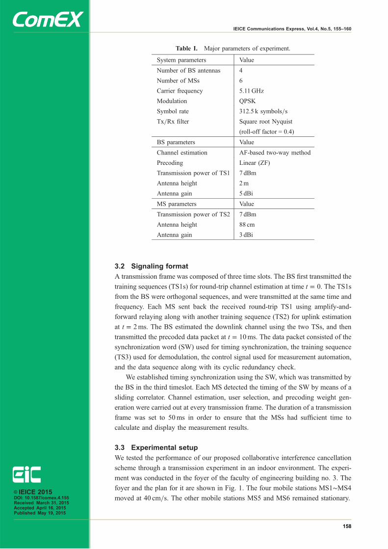
Table I. Major parameters of experiment.
System parameters Value
Number of BS antennas 4
Number of MSs 6
Carrier frequency 5.11GHz
Modulation QPSK
Symbol rate 312.5 k symbols/s
Tx/Rx filter Square root Nyquist
(roll-off factor = 0.4)
BS parameters Value
Channel estimation AF-based two-way method
Precoding Linear (ZF)
Transmission power of TS1 7 dBm
Antenna height 2m
Antenna gain 5 dBi
MS parameters Value
Transmission power of TS2 7 dBm
Antenna height 88 cm
Antenna gain 3 dBi
© IEICE 2015DOI: 10.1587/comex.4.155Received March 31, 2015Accepted April 16, 2015Published May 19, 2015
158
IEICE Communications Express, Vol.4, No.5, 155–160
Wireless LAN modules of the host PCs were employed as collaboration links
among mobile stations. The independent BSS mode channel 48 was used. The
received training signal (TS3) and the received data signal were sampled and
expressed in 20-bit I/Q data streams with 16-bit gain information. Due to possible
packet losses, the number of received signals available for interference cancellation
was not always six. Each MS independently demodulated the available signals. The
performance of the system was evaluated in terms of bit error rate (BER), and data
throughput is beyond the scope of this study.
3.4 Experimental results
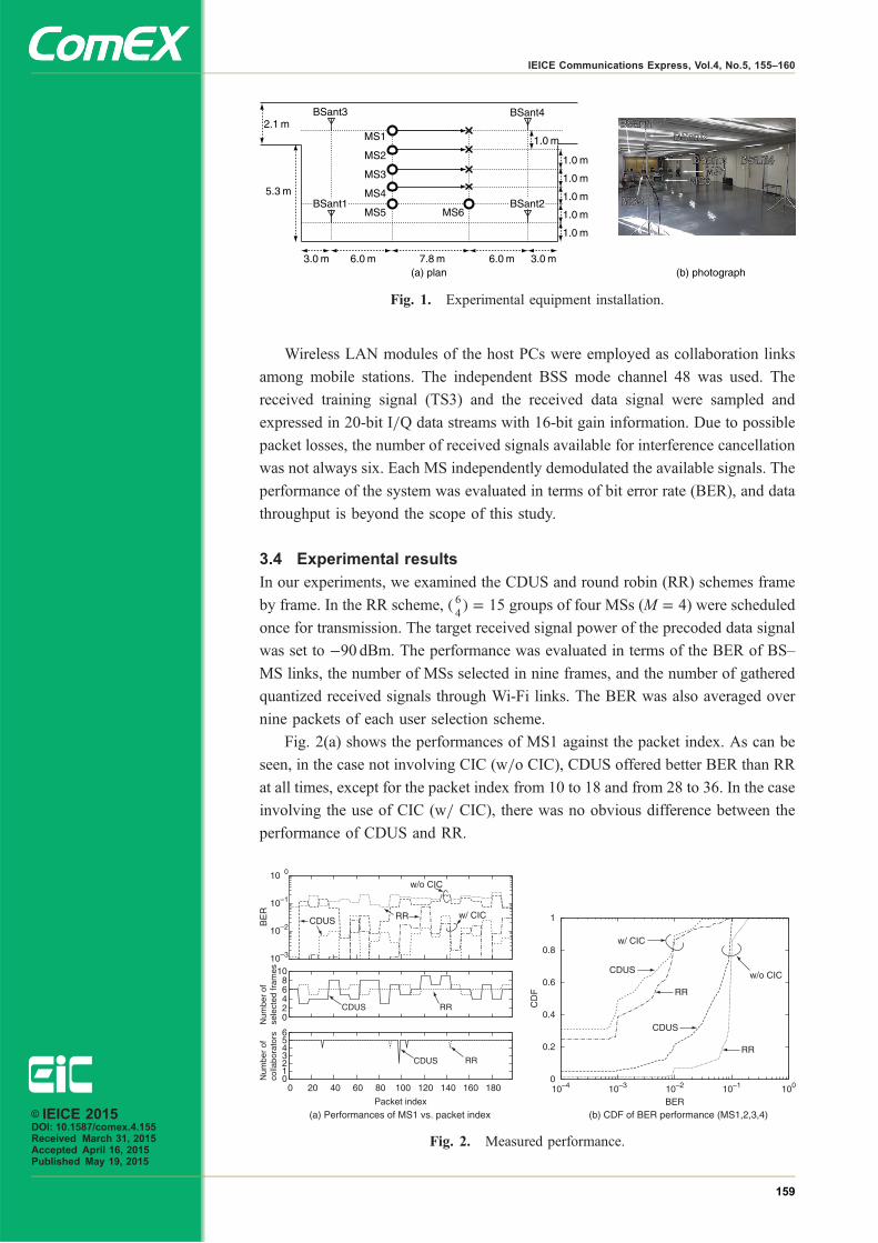
In our experiments, we examined the CDUS and round robin (RR) schemes frame
by frame. In the RR scheme, ð 64Þ ¼ 15 groups of four MSs (M ¼ 4) were scheduled
once for transmission. The target received signal power of the precoded data signal
was set to −90 dBm. The performance was evaluated in terms of the BER of BS–
MS links, the number of MSs selected in nine frames, and the number of gathered
quantized received signals through Wi-Fi links. The BER was also averaged over
nine packets of each user selection scheme.
Fig. 2(a) shows the performances of MS1 against the packet index. As can be
seen, in the case not involving CIC (w/o CIC), CDUS offered better BER than RR
at all times, except for the packet index from 10 to 18 and from 28 to 36. In the case
involving the use of CIC (w/ CIC), there was no obvious difference between the
performance of CDUS and RR.
Fig. 1. Experimental equipment installation.
Fig. 2. Measured performance.
© IEICE 2015DOI: 10.1587/comex.4.155Received March 31, 2015Accepted April 16, 2015Published May 19, 2015
159
IEICE Communications Express, Vol.4, No.5, 155–160
Fig. 2(b) shows the cumulative distribution function (CDF) of the measured
BER of MS1∼MS4. As can be seen from this figure, the collaborative interference
cancellation scheme clearly outperformed independent reception (w/o CIC) for
both the cases involving CDUS and RR. This also confirmed that CDUS is superior
to RR. Moreover, we confirmed that CIC was effective even when a user selection
scheme took orthogonality among users’ channels into account in a user mobility
scenario.
4 Conclusion
In this paper, we applied a collaborative interference cancellation scheme to a ZF-
precoded MU-MIMO system to eliminate residual multi-user interference. Through
a transmission experiment, we confirmed that received signal sharing among
mobile stations can enhance transmission performance, especially among dynamic
mobile stations.
Acknowledgments
This work was supported by the Strategic Information and Communications R&D
Promotion Programme (SCOPE) of the Ministry of Internal Affairs and Commu-
nications, Japan.
© IEICE 2015DOI: 10.1587/comex.4.155Received March 31, 2015Accepted April 16, 2015Published May 19, 2015
160
IEICE Communications Express, Vol.4, No.5, 155–160
Dual polarized open-endedwaveguide using 7-layerPTFE board
Takashi Maruyamaa), Satoshi Yamaguchi, Tomohiro Takahashi,Masataka Otsuka, and Hiroaki MiyashitaInformation Technology R&D Center, Mitsubishi Electric Corporation,
5–1–1 Ofuna, Kamakura, Kanagawa 247–8501, Japan
Abstract: We propose a wideband and dual polarized open-ended wave-
guide for planar array antennas. The proposal forms most of the antenna
structures including waveguide and feeding networks in the dielectric sub-
strates. This yields two advantages. First, it reduces the antenna dimensions
because the waveguide is filled with dielectric; this yields 30% bandwidth
and short element spacing without grating lobes. Second, it simplifies the
machining process, especially for the case of large scale arrays consisting of
several hundred elements. We design antenna elements and a four-element
array, and then fabricate the four-element array using a 7-layer board of
PTFE. Though the calculated and measured reflection characteristics diverge
slightly, the radiation patterns well match.
Keywords: dual polarization, open-ended waveguide, planar array, multi-
layer board
Classification: Antennas and Propagation
References
[1] S. Vaccaro, D. Llorens del Rio, J. Padilla, and R. Baggen, “Low cost Ku-bandelectronic steerable array antenna for mobile satellite communications,” Proc.5th EUCAP, pp. 2362–2366, Apr. 2011.
[2] J. M. Inclán-Alonso, A. García-Aguilar, L. Vigil-Herrero, J. M. FernandezGonzalez, J. SanMartín-Jara, and M. Sierra-Perez, “Portable low profile antennaat X band,” Proc. 5th EUCAP, pp. 2043–2047, Apr. 2011.
[3] H. Arai and T. Izumi, “Wideband dual-polarized small tapered slot antenna forMIMO emulator,” IEEE AP-S, pp. 438–439, 2013. DOI:10.1109/APS.2013.6710880
[4] T. Maruyama, S. Yamaguchi, T. Takahashi, and H. Miyashita, “Design andFabrication of Wideband and Dual Polarized Open-Ended Waveguide,” IEEETrans. Antennas Propag., vol. 62, no. 9, pp. 4872–4876, Sept. 2014. DOI:10.1109/TAP.2014.2333093
© IEICE 2015DOI: 10.1587/comex.4.161Received March 17, 2015Accepted April 21, 2015Published May 19, 2015
161
IEICE Communications Express, Vol.4, No.5, 161–166
1 Introduction
Active phased array antennas (APAA) are attractive for vehicular wireless commu-
nications because of their low profile and lack of moving parts [1]. However, gain
loss for beam scanning is unavoidable and the many RF components raise costs
excessively. Our solution is a mechanically driven planar array where all elements
are excited in phase. Our goal is to realize a mechanically driven planar array
yielding dual polarization and 30% frequency bandwidth. Because the array
antenna with several hundred elements is required for high gain, the antenna
structure must be easy to make. Because all elements are connected to a passive
beam forming network, low loss antenna elements are also required. This paper
proposes solutions to meet all of these requirements.
The first candidate for an array element with wideband and dual polarization is
the stacked patch antenna [2]. It has simple structure and it may achieve 30%
bandwidth. Unfortunately, relatively large conductor loss and dielectric loss are
unavoidable. The second candidate is the tapered slot antenna [3]. It is suitable for
array antennas because it can be fabricated on the dielectric substrate. Unfortu-
nately, its dimension on the boresight axis is relatively long. Moreover, large scale
arrays are hard to manufacture because the many substrates must be aligned in grid
pattern.
We focused on the open-ended waveguide in earlier work [4]. Our design
places strip lines in the substrate to feed the multiple elements. We designed the
antenna and confirmed that the calculated and measured results agree well.
However, it has two issues. The first one is antenna size. Waveguide size must
be 0:5�l or wider to pass the dominant mode, where �l is the wavelength at the
lower limit frequency. On the other hand, antenna spacing must be 1:0�h or shorter
to avoid grating lobes, where �h is the wavelength at the upper limit frequency. Our
design has difficulty in satisfying both constraints due to waveguide size. The
second issue is manufacturing complexity. The design stacks multiple metal parts
and dielectric substrates which raises machining and assembly costs. Additionally,
it was difficult to connect the signal line from the antenna bottom to the strip line
because the line must pass through metal parts and dielectric substrates. In this
paper, we drastically change the antenna structure. Most antenna structures,
including the waveguide and feeding circuits, are formed in the multi-layer board.
We fabricate 7-layer board of PTFE substrates to reduce dielectric loss. Though
PTFE multi-layer boards are not common due to their viscosity, this structure has
significant advantages. The antenna dimensions are reduced because the waveguide
is filled with dielectric. This achieves the 30% frequency bandwidth and the
antenna spacing of 1:0�h or shorter. Additionally, when several hundred elements
are required, the machining process can be reduced because etching is used. The
vertical signal line from the antenna bottom to the strip line is also easily realized
by through holes formed when fabricating the multi-layer board. We designed the
antenna element and four-element array with antenna spacing of 1:0�h or shorter.
We fabricated the four-element array. Though there was some discrepancy between
the calculated and measured reflection characteristics, the radiation patterns agreed
well.© IEICE 2015DOI: 10.1587/comex.4.161Received March 17, 2015Accepted April 21, 2015Published May 19, 2015
162
IEICE Communications Express, Vol.4, No.5, 161–166
2 Antenna structure
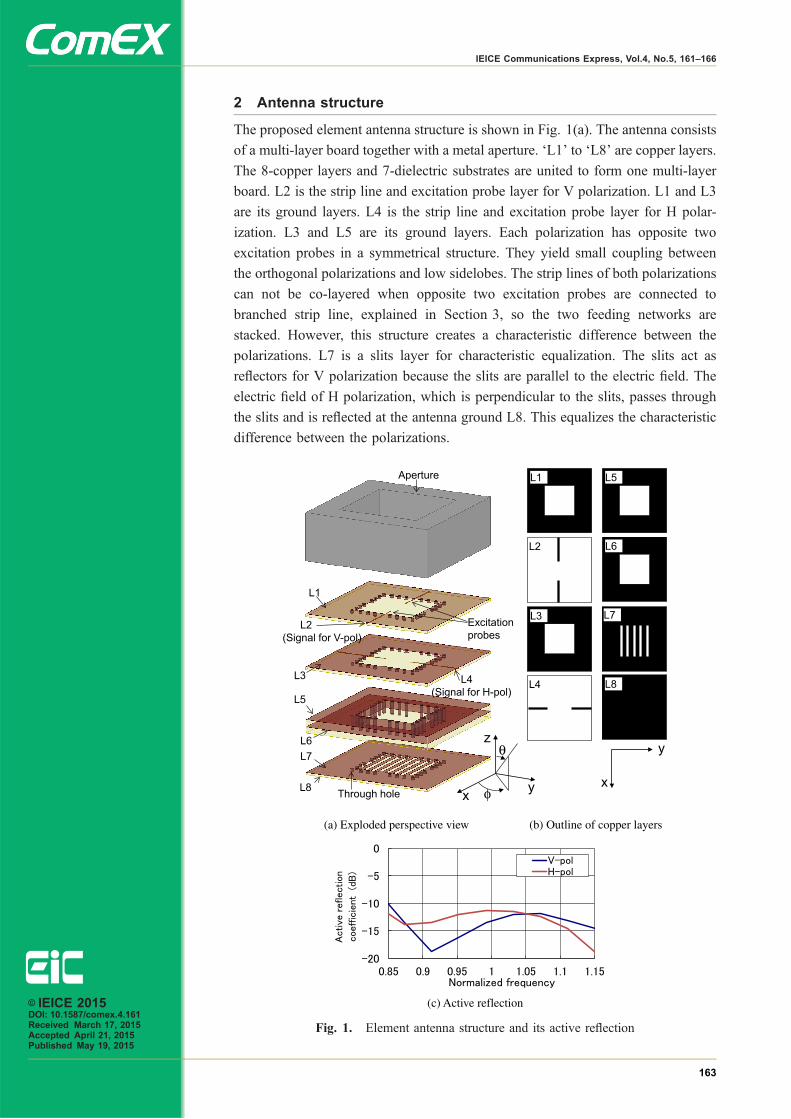
The proposed element antenna structure is shown in Fig. 1(a). The antenna consists
of a multi-layer board together with a metal aperture. ‘L1’ to ‘L8’ are copper layers.
The 8-copper layers and 7-dielectric substrates are united to form one multi-layer
board. L2 is the strip line and excitation probe layer for V polarization. L1 and L3
are its ground layers. L4 is the strip line and excitation probe layer for H polar-
ization. L3 and L5 are its ground layers. Each polarization has opposite two
excitation probes in a symmetrical structure. They yield small coupling between
the orthogonal polarizations and low sidelobes. The strip lines of both polarizations
can not be co-layered when opposite two excitation probes are connected to
branched strip line, explained in Section 3, so the two feeding networks are
stacked. However, this structure creates a characteristic difference between the
polarizations. L7 is a slits layer for characteristic equalization. The slits act as
reflectors for V polarization because the slits are parallel to the electric field. The
electric field of H polarization, which is perpendicular to the slits, passes through
the slits and is reflected at the antenna ground L8. This equalizes the characteristic
difference between the polarizations.
(a) Exploded perspective view (b) Outline of copper layers
(c) Active reflection
Fig. 1. Element antenna structure and its active reflection
© IEICE 2015DOI: 10.1587/comex.4.161Received March 17, 2015Accepted April 21, 2015Published May 19, 2015
163
IEICE Communications Express, Vol.4, No.5, 161–166
We designed the antenna element using HFSS, an electromagnetic field
simulator. The dielectric substrate is PTFE composite with the relative permittivity
of around 2.1. The calculation model has four feeding points at the edge of strip
lines. The aperture size is 0:79�, where λ is center frequency wavelength. This
corresponds to 0:91�h. The waveguide size, the white square in L1, 3, 5, 6, is 0:58�.
It corresponds to 0:49�l. In the proposed antenna, the waveguide size is mini-
aturized because the waveguide is filled with PTFE; the remaining space holds the
strip line. Its design is shown in Section 3. Through holes are placed to form the
conducting walls of the waveguide. The probe length is adjusted so as to decrease
reflection. The length was 0:29� for V polarization and 0:31� for H polarization.
Fig. 1(c) shows the active reflection plots. The plot of V-pol (H-pol) means the
active reflection yielded when the two signal lines of L2 (L4) are excited in
reversed phase. The two plots are similar due to L7 slits. The active reflection
value is −10 dB or lower for both polarizations in the 30% bandwidth.
3 Design of four-element array
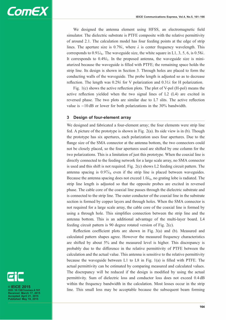
We designed and fabricated a four-element array; the four elements were strip line
fed. A picture of the prototype is shown in Fig. 2(a). Its side view is in (b). Though
the prototype has six apertures, each polarization uses four apertures. Due to the
flange size of the SMA connector at the antenna bottom, the two connectors could
not be closely placed, so the four apertures used are shifted by one column for the
two polarizations. This is a limitation of just this prototype. When the coaxial line is
directly connected to the feeding network for a large scale array, no SMA connector
is used and this shift is not required. Fig. 2(c) shows L2 feeding circuit pattern. The
antenna spacing is 0:97�h even if the strip line is placed between waveguides.
Because the antenna spacing does not exceed 1:0�h, no grating lobe is radiated. The
strip line length is adjusted so that the opposite probes are excited in reversed
phase. The cable core of the coaxial line passes through the dielectric substrate and
is connected to the strip line. The outer conductor of the coaxial line in the substrate
section is formed by copper layers and through holes. When the SMA connector is
not required for a large scale array, the cable core of the coaxial line is formed by
using a through hole. This simplifies connection between the strip line and the
antenna bottom. This is an additional advantage of the multi-layer board. L4
feeding circuit pattern is 90 degree rotated version of Fig. 2(c).
Reflection coefficient plots are shown in Fig. 3(a) and (b). Measured and
calculated pattern shapes agree. However the measured frequency characteristics
are shifted by about 5% and the measured level is higher. This discrepancy is
probably due to the difference in the relative permittivity of PTFE between the
calculation and the actual value. This antenna is sensitive to the relative permittivity
because the waveguide between L1 to L8 in Fig. 1(a) is filled with PTFE. The
actual permittivity can be estimated by comparing measured and calculated values.
The discrepancy will be reduced if the design is modified by using the actual
permittivity. Sum of dielectric loss and conductor loss does not exceed 0.4 dB
within the frequency bandwidth in the calculation. Most losses occur in the strip
line. This small loss may be acceptable because the subsequent beam forming© IEICE 2015DOI: 10.1587/comex.4.161Received March 17, 2015Accepted April 21, 2015Published May 19, 2015
164
IEICE Communications Express, Vol.4, No.5, 161–166
network is simplified even for large scale arrays. Fig. 3(c) and (d) are radiation
patterns at the center frequency when the V polarization feeding circuit is excited.
Fig. 3(e) and (f ) are radiation patterns at the upper limit frequency; they show that
no grating lobe is observed. Calculated and measured patterns approximately
agreed including the cross polarization pattern. The worst cross polarization value
on the boresight was −34 dB. Radiation patterns of H polarization were similar to
(but rotated) those of V polarization.
(a) Picture of four-element array (b) Side view
(Each polarization uses four apertures)
(c) Feeding circuit
Fig. 2. Four-element array
© IEICE 2015DOI: 10.1587/comex.4.161Received March 17, 2015Accepted April 21, 2015Published May 19, 2015
165
IEICE Communications Express, Vol.4, No.5, 161–166
4 Conclusion
We proposed a wideband and dual polarized open-ended waveguide for array
antennas. Most antenna structures including strip lines and waveguide cavity are
formed in a multi-layer board. A slits structure to equalize the frequency character-
istics of polarizations is also included. This structure enables both 30% bandwidth
and small antenna spacing because the waveguide is filled with dielectric. We
designed and fabricated a four-element array with no grating lobes within the 30%
bandwidth. Though the measured frequency characteristics of the reflection differed
by about 5% due to a difference in the relative permittivity value assumed, the
calculated and measured radiation patterns approximately agreed.
(a) Reflection of V polarization (b) Reflection of H polarization
(c) Radiation pattern (φ=0deg, Fc)
(e) Radiation pattern (φ=0deg, Fh)
(d) Radiation pattern (φ=90deg, Fc)
(f) Radiation pattern (φ=90deg, Fh)
Fig. 3. Measured and calculated results
© IEICE 2015DOI: 10.1587/comex.4.161Received March 17, 2015Accepted April 21, 2015Published May 19, 2015
166
IEICE Communications Express, Vol.4, No.5, 161–166
Feasibility of RSSI based60GHz WLAN discovery formulti-band WLAN
Sho Wadaa), Masahiro Umehirab), Shigeki Takedac),Teruyuki Miyajimad), and Kenichi Kagoshimae)
College of Engineering, Ibaraki University,
4–12–1 Nakanarusawa-cho, Hitachi-shi, Ibaraki, Japan
Abstract: This letter proposes RSSI (Received Signal Strength Indicator)
based 60GHz WLAN discovery for multiband WLAN (Wireless LAN),
which uses both 2.4/5GHz band and 60GHz band to achieve high trans-
mission speed, sufficient reliability and power-saving of a multiband WLAN
device. The proposed 60GHz WLAN discovery detects 60GHz WLAN
coverage by using RSSI of 2.4/5GHz WLAN signals. Space/time diversity
is employed to improve the false detection probability of 60GHz WLAN
discovery. Ray-tracing simulation results confirm that 60GHz WLAN dis-
covery is feasible and space/time diversity is effective to improve the
reliability of 60GHz WLAN discovery.
Keywords: RSSI, multiband WLAN, 60GHz, space/time diversity
Classification: Wireless Communication Technologies
References
[1] I. Toyoda, F. Nuno, Y. Shimizu, and M. Umehira, “Proposal of 5/25-GHz dualband OFDM-based wireless LAN for high-capacity broadband communica-tions,” PIMRC 2005, vol. 3, pp. 2104–2108, Sept. 2005. DOI:10.1109/PIMRC.2005.1651810
[2] M. de Courville, S. Zeisberg, M. Muck, and J. Schönthier, “IST Project:BroadWay—The way to broadband access at 60GHz,” PWC 2003, vol. 2775,pp. 219–221, Sept. 2003. DOI:10.1007/978-3-540-39867-7_24
[3] H. Singh, J. Hsu, L. Verma, S. S. Lee, and C. Ngo, “Green operation of multi-band wireless LAN in 60GHz and 2.4/5GHz,” CCNC 2011, pp. 787–792, Jan.2011. DOI:10.1109/CCNC.2011.5766599
[4] M. Umehira, G. Saito, S. Wada, S. Takeda, T. Miyajima, and K. Kagoshima,“Feasibility of RSSI based access network detection for multi-band WLANusing 2.4/5GHz and 60GHz,” WPMC 2014, pp. 243–248, Sept. 2014. DOI:10.1109/WPMC.2014.7014824
[5] EEM Inc., “EEM-RTM,” http://www.e-em.co.jp/rtm/eem_rtm.htm (2014/2/1access) (in Japanese).© IEICE 2015
DOI: 10.1587/comex.4.167Received April 3, 2015Accepted April 14, 2015Published May 28, 2015
167
IEICE Communications Express, Vol.4, No.5, 167–172
1 Introduction
Multiband WLAN using both 2.4/5GHz and 60GHz or other higher frequency
band has been proposed to achieve both high transmission speed and sufficient
reliability [1, 2, 3]. In the multiband WLAN, 60GHz is used to achieve high
transmission speed and 2.4/5GHz is used if 60GHz is unavailable due to human
body shadowing for example. Power-saving is an important issue for a battery-
operated multiband WLAN device because power consumption of the multiband
WLAN device can be very large if both 2.4/5GHz and 60GHz radio parts are
always turned on. Therefore, a novel power saving technique is needed to turn on
60GHz radio only if the multiband WLAN device is within 60GHz WLAN
coverage. This is a spectrum efficient approach if 60GHz is used instead of
2.4/5GHz as far as 60GHz can be used. This usage scenario requires a multiband
WLAN device to detect 60GHz WLAN coverage using 2.4/5GHz WLAN radio
instead of 60GHz WLAN radio [4].
This letter proposes RSSI based 60GHz WLAN discovery for multi-band
WLAN, by using 2.4/5GHz WLAN signals without using 60GHz WLAN radio.
Assuming that a line-of-sight (LOS) path is available in 60GHz WLAN, we can
expect LOS path is also available in 2.4/5GHz, thus, 60GHz RSSI is in proportion
to 2.4/5GHz RSSI. However, multi-path propagation in 2.4/5GHz WLAN can
cause 2.4/5GHz RSSI variation, and degrade miss- and false-detection of 60GHz
WLAN coverage. To solve this problem, we introduce space/time diversity to
improve the reliability of 60GHz WLAN discovery. Ray-tracing simulation results
confirm that 60GHz WLAN discovery is feasible and space/time diversity is
effective to improve the reliability of 60GHz WLAN discovery.
2 Operation of multiband WLAN
We assume that multiband WLAN AP (Access Point) and STA (Station) have both
2.4/5GHz and 60GHz radio parts. As 2.4/5GHz WLAN has wider coverage than
60GHz WLAN, 2.4/5GHz WLAN can be used whenever 60GHz WLAN can be
used. A multiband WLAN AP always uses both 2.4/5GHz and 60GHz radio parts,
however 60GHz radio part needs to be turned-off or in a sleep mode when a
multiband WLAN STA is out of 60GHz WLAN coverage. 60GHz radio part is
turned on or waked up as soon as 60GHz WLAN coverage is detected and 60GHz
link is used to provide high transmission rate as far as 60GHz link is available. If
60GHz link is blocked due to moving human body for example, wireless con-
nection is immediately switched from 60GHz to 2.4/5GHz to maintain the
wireless connection. This operation strategy of multiband WLAN enables to
efficiently utilize valuable 2.4/5GHz spectrum in combination with 60GHz.
3 Principle of RSSI based 60GHz WLAN discovery
Since a directional antenna is used and LOS is maintained in 60GHz WLAN, we
can assume that propagation of 60GHz WLAN is almost free space propagation,
where a direct wave is dominant and received level of other reflected waves are
much smaller than that of a direct wave. Friis formula can be used to calculate
received signal power of 60GHz, Pr60G, which is given by:
© IEICE 2015DOI: 10.1587/comex.4.167Received April 3, 2015Accepted April 14, 2015Published May 28, 2015
168
IEICE Communications Express, Vol.4, No.5, 167–172
Pr60G ¼ �60G4�r
� �2
Pt60GGt60GGr60G; ð1Þ
where r is the distance between a transmitter and a receiver, �60G is wavelength of
60GHz and Pt60G is transmission power. Gt60G and Gr60G are antenna gain of a
transmitter and a receiver.
In a multiband WLAN STA using 2.4GHz and 60GHz, LOS is maintained and
a direct wave is dominant in 2.4GHz if STA is within 60GHz WLAN coverage.
However, as omni-directional antenna is generally used in 2.4GHz WLAN,
2.4GHz RSSI can vary more than 60GHz RSSI due to multi-path propagation.
In this case, the instantaneous received power at 2.4GHz, P is given by:
P ¼ 1
2ErðtÞErðtÞ� ¼ 1
2
Xkm¼0
Amej!ðt��mÞ
! Xkm¼0
Amej!ðt��mÞ
!�
¼Xkm¼0
Am2
2þXk�1m0¼0
Xkm¼m0
AmAm0 cos!ð�m0 � �mÞ;ð2Þ
where ErðtÞ is electric field strength at the receiver, Am is amplitude of the m-th
path, �m is delay time of the m-th path, k is the number of multi-paths, and m ¼ 0
means a direct wave. In this equation, the first term means averaged RSSI and the
second term means RSSI variation due to multi-path propagation. The second term
becomes zero if averaging is performed with sufficiently large number of samples.
Averaged received signal power of 2.4GHz, Pr2:4G is approximated by:
Pr2:4G ¼ Pt2:4GGt2:4GGr2:4G
Xkm¼0
�2:4G4�rm
� �2
R2m
!ffi Pt2:4GGt2:4GGr2:4G
�2:4G4�r0
� �2
; ð3Þ
where �2:4G is wavelength of 2.4GHz and Pt2:4G is transmission power. Gt2:4G and
Gr2:4G are antenna gain of a transmitter and a receiver, and Rm is reflection
coefficient of the m-th path. In LOS propagation condition in 2.4GHz WLAN,
received level of a direct wave is assumed to be larger than that of other reflected
waves. As Pt60G, Gt60G, Gr60G, Pt2:4G, Gt2:4G, and Gr2:4G are known design parame-
ters, we obtain the following equation from the Eq. (1) and (3):
Pr60G ¼ Pr2:4G�260GPt60GGt60GGr60G
�22:4GPt2:4GGt2:4GGr2:4Gð4Þ
This equation indicates that 60GHz RSSI can be estimated by averaging multiple
samples of 2.4GHz RSSI in LOS condition. However, we need various 2.4GHz
RSSI samples in various propagation conditions for averaging. We propose to apply
diversity techniques for this purpose. Supposing that N is the number of space
diversity branches and M is the number of time diversity branches, the total number
of diversity branches, L is given by N �M and L samples of 2.4GHz RSSI can be
averaged to estimate 60GHz RSSI. Based on Eq. (4), the estimated received power
Pr2:4G is given by:
Pr2:4G ¼ 10 log101
L
XLi¼1
10PR2:4GðiÞ
10
!½dB� ð5Þ
where PR2:4GðiÞ is the measured RSSI at each diversity branch i.© IEICE 2015DOI: 10.1587/comex.4.167Received April 3, 2015Accepted April 14, 2015Published May 28, 2015
169
IEICE Communications Express, Vol.4, No.5, 167–172
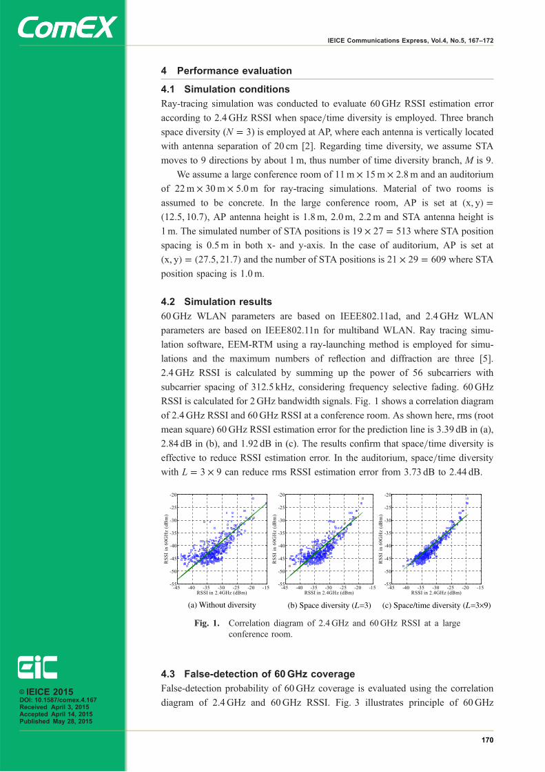
4 Performance evaluation
4.1 Simulation conditions
Ray-tracing simulation was conducted to evaluate 60GHz RSSI estimation error
according to 2.4GHz RSSI when space/time diversity is employed. Three branch
space diversity (N ¼ 3) is employed at AP, where each antenna is vertically located
with antenna separation of 20 cm [2]. Regarding time diversity, we assume STA
moves to 9 directions by about 1m, thus number of time diversity branch, M is 9.
We assume a large conference room of 11m � 15m � 2:8m and an auditorium
of 22m � 30m � 5:0m for ray-tracing simulations. Material of two rooms is
assumed to be concrete. In the large conference room, AP is set at ðx; yÞ ¼ð12:5; 10:7Þ, AP antenna height is 1.8m, 2.0m, 2.2m and STA antenna height is
1m. The simulated number of STA positions is 19 � 27 ¼ 513 where STA position
spacing is 0.5m in both x- and y-axis. In the case of auditorium, AP is set at
ðx; yÞ ¼ ð27:5; 21:7Þ and the number of STA positions is 21 � 29 ¼ 609 where STA
position spacing is 1.0m.
4.2 Simulation results
60GHz WLAN parameters are based on IEEE802.11ad, and 2.4GHz WLAN
parameters are based on IEEE802.11n for multiband WLAN. Ray tracing simu-
lation software, EEM-RTM using a ray-launching method is employed for simu-
lations and the maximum numbers of reflection and diffraction are three [5].
2.4GHz RSSI is calculated by summing up the power of 56 subcarriers with
subcarrier spacing of 312.5 kHz, considering frequency selective fading. 60GHz
RSSI is calculated for 2GHz bandwidth signals. Fig. 1 shows a correlation diagram
of 2.4GHz RSSI and 60GHz RSSI at a conference room. As shown here, rms (root
mean square) 60GHz RSSI estimation error for the prediction line is 3.39 dB in (a),
2.84 dB in (b), and 1.92 dB in (c). The results confirm that space/time diversity is
effective to reduce RSSI estimation error. In the auditorium, space/time diversity
with L ¼ 3 � 9 can reduce rms RSSI estimation error from 3.73 dB to 2.44 dB.
4.3 False-detection of 60GHz coverage
False-detection probability of 60GHz coverage is evaluated using the correlation
diagram of 2.4GHz and 60GHz RSSI. Fig. 3 illustrates principle of 60GHz
(a) Without diversity (c) Space/time diversity (L =3×9)(b) Space diversity (L =3)
Fig. 1. Correlation diagram of 2.4GHz and 60GHz RSSI at a largeconference room.
© IEICE 2015DOI: 10.1587/comex.4.167Received April 3, 2015Accepted April 14, 2015Published May 28, 2015
170
IEICE Communications Express, Vol.4, No.5, 167–172
coverage estimation by using 2.4GHz RSSI. Supposing that 60GHz coverage
needs the received power more than −45 dBm, the correlation diagram is divided
into four areas. Area (2) and (3) mean correct detections, i.e. “within 60GHz
coverage” and “out of 60GHz coverage”. Area (1) means miss detection, i.e.
“60GHz cannot be used though it can be used”, and area (4) means false-detection,
i.e. “60GHz can be used though it cannot be used”. If false detection happens,
60GHz RF part is turned on though 60GHz WLAN is unavailable, thus battery
power is wasted. False detection probability can be reduced by introducing
detection threshold margin as shown in Fig. 3. Large detection margin can reduce
false detection but increase miss detection. Miss detection and false detection is a
trade-off issue and larger detection margin makes 60GHz coverage effectively
smaller. Therefore, detection margin should be as small as possible.
Fig. 3 shows false detection probability as a function of detection threshold
margin. The results show that space/time diversity decreases the detection thresh-
old margin by 2 dB in the conference room and by 1.5 dB in the auditorium. This
means that 60GHz coverage can be increased by 41%∼58% while the false-
detection probability is maintained at 0.05 or 0.02.
Fig. 2. Principle of 60GHz coverage estimation by 2.4GHz RSSI.
Fig. 3. False detection probability as a function of detection thresholdmargin.
© IEICE 2015DOI: 10.1587/comex.4.167Received April 3, 2015Accepted April 14, 2015Published May 28, 2015
171
IEICE Communications Express, Vol.4, No.5, 167–172
5 Conclusion
This letter proposes RSSI based 60GHz WLAN discovery for multi-band WLAN.
Ray-tracing simulation results confirm that RSSI based 60GHz WLAN discovery
is feasible and space/time diversity is effective to improve detection reliability.
Acknowledgments
This work is supported by the Ministry of Internal Affairs and Communications of
Japan, under the grant of research and development for radio resource enhance-
ment, “multi-band/multi-mode sensor wireless communications technologies”.
© IEICE 2015DOI: 10.1587/comex.4.167Received April 3, 2015Accepted April 14, 2015Published May 28, 2015
172
IEICE Communications Express, Vol.4, No.5, 167–172


![IEICE Communications Society GLOBAL NEWSLETTER Vol. 6[IEICE Sponsored Conference] IEICE Communications Society – GLOBAL NEWSLETTER Vol. 6 lecturers are invited to introduce recent](https://img.pdfslide.us/doc/110x75/5feb39fbc31fbc18b814ecc5/ieice-communications-society-global-newsletter-vol-6-ieice-sponsored-conference.jpg)


![IEICE Communications Society GLOBAL NEWSLETTER Vol… · · 2005-06-27[From IEICE Communications Society Fellows] IEICE Communications Society – GLOBAL NEWSLETTER Vol. 2](https://img.pdfslide.us/doc/110x75/5ade06827f8b9aa5088d9d36/ieice-communications-society-global-newsletter-vol-from-ieice-communications.jpg)
![IEICE Communications Society GLOBAL … 2011,IEICE [Contents] IEICE Communications Society – GLOBAL NEWSLETTER Vol. 35, No. 1 IEICE Communications Society GLOBAL NEWSLETTER Vol](https://img.pdfslide.us/doc/110x75/5ae27cfe7f8b9a5d648cc037/ieice-communications-society-global-2011ieice-contents-ieice-communications.jpg)