Embed Size (px)
Citation preview

Design Note DN 2013-01
V1.0 January 2013
CCM PFC Boost Converter Design
Sam Abdel-Rahman
Infineon Technologies North America (IFNA) Corp.

CCM PFC Boost Converter Design
2
Design Note DN 2013-01
V1.0 January 2013
Edition 2013-01-01 Published by Infineon Technologies North America 27703 Emperor Blvd, suite 310, Durham, NC 27703 © Infineon Technologies North America Corp. 2013 All Rights Reserved.
Attention please!
THE INFORMATION GIVEN IN THIS APPLICATION NOTE IS GIVEN AS A HINT FOR THE IMPLEMEN-TATION OF THE INFINEON TECHNOLOGIES COMPONENT ONLY AND SHALL NOT BE REGARDED AS ANY DESCRIPTION OR WARRANTY OF A CERTAIN FUNCTIONALITY, CONDITION OR QUALITY OF THE INFINEON TECHNOLOGIES COMPONENT. THE RECIPIENT OF THIS APPLICATION NOTE MUST VERIFY ANY FUNCTION DESCRIBED HEREIN IN THE REAL APPLICATION. INFINEON TECHNOLOGIES HEREBY DISCLAIMS ANY AND ALL WARRANTIES AND LIABILITIES OF ANY KIND (INCLUDING WITHOUT LIMITATION WARRANTIES OF NON-INFRINGEMENT OF INTELLECTUAL PROPERTY RIGHTS OF ANY THIRD PARTY) WITH RESPECT TO ANY AND ALL INFORMATION GIVEN IN THIS APPLICATION NOTE.
Information
For further information on technology, delivery terms and conditions and prices please contact your
nearest Infineon Technologies Office (www.infineon.com).
Warnings
Due to technical requirements components may contain dangerous substances. For information on the
types in question please contact your nearest Infineon Technologies Office. Infineon Technologies
Components may only be used in life-support devices or systems with the express written approval of
Infineon Technologies, if a failure of such components can reasonably be expected to cause the failure of
that life-support device or system, or to affect the safety or effectiveness of that device or system. Life
support devices or systems are intended to be implanted in the human body, or to support and/or maintain
and sustain and/or protect human life. If they fail, it is reasonable to assume that the health of the user or
other persons may be endangered.
DN 2013-01
Subjects: CCM PFC Boost Converter Design Author: Sam Abdel-Rahman (IFNA PMM SMD AMR PMD 2) We Listen to Your Comments
Any information within this document that you feel is wrong, unclear or missing at all? Your feedback will help us to continuously improve the quality of this document. Please send your proposal (including a reference to this document) to: [[email protected]]
CCM PFC Boost Converter Design
3
Design Note DN 2013-01
V1.0 January 2013
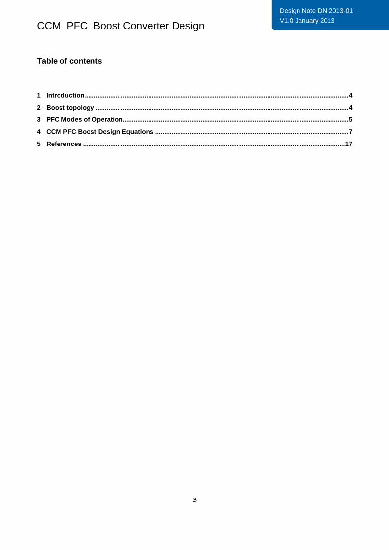
Table of contents
1 Introduction .................................................................................................................................................. 4
2 Boost topology ............................................................................................................................................ 4
3 PFC Modes of Operation ............................................................................................................................. 5
4 CCM PFC Boost Design Equations ........................................................................................................... 7
5 References ................................................................................................................................................. 17
CCM PFC Boost Converter Design
4
Design Note DN 2013-01
V1.0 January 2013
1 Introduction
Power Factor Correction (PFC) shapes the input current of the power supply to be in synchronization with the mains voltage, in order to maximize the real power drawn from the mains. In a perfect PFC circuit, the input current follows the input voltage as would an equivalent resistor, with no added input current harmonics. This document is intended to discuss the topology and operational mode for high power PFC applications (>300W), and provide detailed design equations with examples.
2 Boost topology
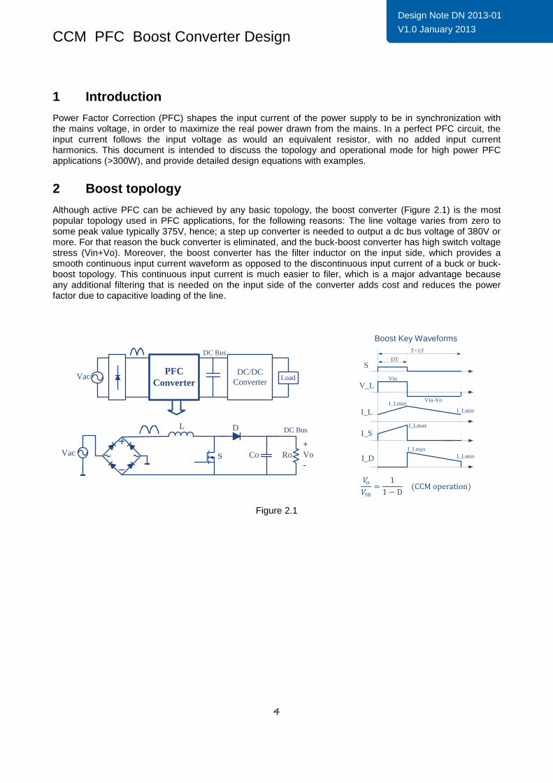
Although active PFC can be achieved by any basic topology, the boost converter (Figure 2.1) is the most popular topology used in PFC applications, for the following reasons: The line voltage varies from zero to some peak value typically 375V, hence; a step up converter is needed to output a dc bus voltage of 380V or more. For that reason the buck converter is eliminated, and the buck-boost converter has high switch voltage stress (Vin+Vo). Moreover, the boost converter has the filter inductor on the input side, which provides a smooth continuous input current waveform as opposed to the discontinuous input current of a buck or buck-boost topology. This continuous input current is much easier to filer, which is a major advantage because any additional filtering that is needed on the input side of the converter adds cost and reduces the power factor due to capacitive loading of the line.
Boost Key Waveforms
Figure 2.1
AC
PFC
Converter
DC/DC
ConverterLoad
DC Bus
Vac
AC
L D
RoVac CoS
+
Vo
-
DC Bus
S
V_L
I_L
I_S
I_D
T=1/f
DT
Vin
Vin-VoI_Lmax
I_Lmin
I_Lmax
I_Lmax
I_Lmin
CCM PFC Boost Converter Design
5
Design Note DN 2013-01
V1.0 January 2013
3 PFC Modes of Operation
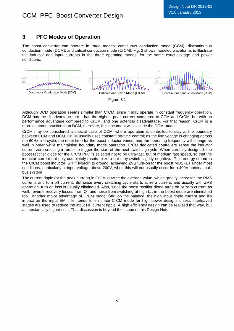
The boost converter can operate in three modes: continuous conduction mode (CCM), discontinuous conduction mode (DCM), and critical conduction mode (CrCM). Fig. 2 shows modeled waveforms to illustrate the inductor and input currents in the three operating modes, for the same exact voltage and power conditions.
0 1 104-
2 104-
3 104-
4 104-
0
5
10
15
Iin t( )
IL t( )
tContinuous Conduction Mode (CCM)
0 1 104-
2 104-
3 104-
4 104-
0
5
10
15
Iin t( )
IL t( )
tDiscontinuous Conduction Mode (DCM)
Figure 3.1
Although DCM operation seems simpler than CrCM, since it may operate in constant frequency operation, DCM has the disadvantage that it has the highest peak current compared to CCM and CrCM, but with no performance advantage compared to CrCM, and one potential disadvantage. For that reason, CrCM is a more common practice than DCM, therefore, this document will exclude the DCM mode.
CrCM may be considered a special case of CCM, where operation is controlled to stay at the boundary between CCM and DCM. CrCM usually uses constant on-time control; as the line voltage is changing across the 60Hz line cycle, the reset time for the boost inductor varies, and the operating frequency will change as well in order while maintaining boundary mode operation. CrCM dedicated controllers sense the inductor current zero crossing in order to trigger the start of the next switching cycle. When carefully designed, the boost rectifier diode for the CrCM PFC is selected not to be ultra-fast, but of medium fast speed, so that the inductor current not only completely resets to zero but may switch slightly negative. This energy stored in the CrCM boost inductor will “Flyback” to ground, achieving ZVS turn-on for the boost MOSFET under most conditions, particularly at input voltage above 200V, when this will not usually occur for a 400V nominal bulk bus system.
The current ripple (or the peak current) in CrCM is twice the average value, which greatly increases the RMS currents and turn off current. But since every switching cycle starts at zero current, and usually with ZVS operation, turn on loss is usually eliminated. Also, since the boost rectifier diode turns off at zero current as well, reverse recovery losses from Qrr and noise from switching at high Irrm in the boost diode are eliminated too, another major advantage of CrCM mode. Still, on the balance, the high input ripple current and it’s impact on the input EMI filter tends to eliminate CrCM mode for high power designs unless interleaved stages are used to reduce the input HF current ripple. A high efficiency design can be realized that way, but at substantially higher cost. That discussion is beyond the scope of this Design Note.
0 1 104-
2 104-
3 104-
4 104-
0
5
10
15
Iin t( )
IL t( )
tCritical Conduction Mode (CrCM)
CCM PFC Boost Converter Design
6
Design Note DN 2013-01
V1.0 January 2013
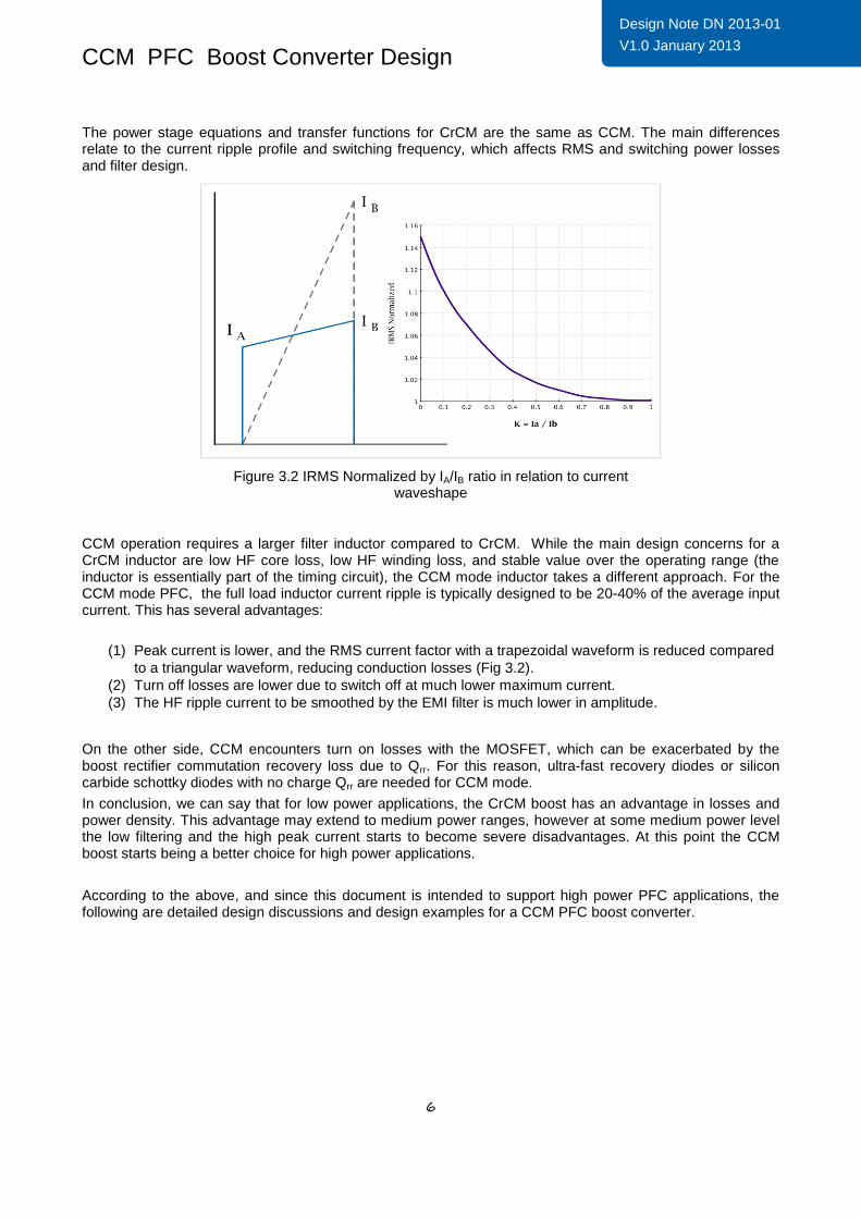
The power stage equations and transfer functions for CrCM are the same as CCM. The main differences relate to the current ripple profile and switching frequency, which affects RMS and switching power losses and filter design.
Figure 3.2 IRMS Normalized by IA/IB ratio in relation to current waveshape
CCM operation requires a larger filter inductor compared to CrCM. While the main design concerns for a CrCM inductor are low HF core loss, low HF winding loss, and stable value over the operating range (the inductor is essentially part of the timing circuit), the CCM mode inductor takes a different approach. For the CCM mode PFC, the full load inductor current ripple is typically designed to be 20-40% of the average input current. This has several advantages:
(1) Peak current is lower, and the RMS current factor with a trapezoidal waveform is reduced compared
to a triangular waveform, reducing conduction losses (Fig 3.2).
(2) Turn off losses are lower due to switch off at much lower maximum current.
(3) The HF ripple current to be smoothed by the EMI filter is much lower in amplitude.
On the other side, CCM encounters turn on losses with the MOSFET, which can be exacerbated by the boost rectifier commutation recovery loss due to Qrr. For this reason, ultra-fast recovery diodes or silicon carbide schottky diodes with no charge Qrr are needed for CCM mode.
In conclusion, we can say that for low power applications, the CrCM boost has an advantage in losses and power density. This advantage may extend to medium power ranges, however at some medium power level the low filtering and the high peak current starts to become severe disadvantages. At this point the CCM boost starts being a better choice for high power applications.
According to the above, and since this document is intended to support high power PFC applications, the following are detailed design discussions and design examples for a CCM PFC boost converter.
CCM PFC Boost Converter Design
7
Design Note DN 2013-01
V1.0 January 2013
4 CCM PFC Boost Design Equations
The following are design equations for the CCM operated boost, with a design example integrated to further clarify the usage of all equations. The boost converter encounters the maximum current stress and power
losses at the minimum line voltage condition ( ); hence, all design equations and power losses will be
calculated using the low line voltage condition.
Table 1 Specifications
Input voltage 85-265 VAC 60Hz
Output voltage 390V
Maximum power steady state 400W
Switching frequency 100kHz
Inductor current ripple 30%
Output voltage ripple (2x line frequency) 10 Vp-p
Hold-up time 16.6ms @ VO.min=350V
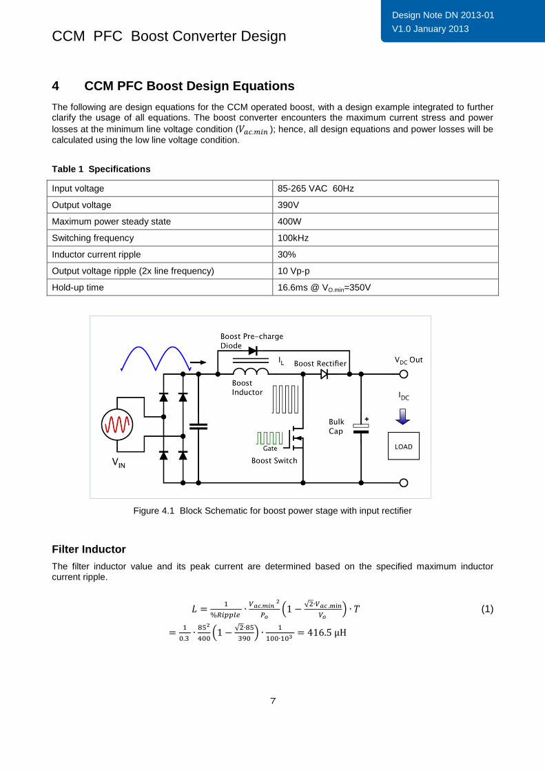
Figure 4.1 Block Schematic for boost power stage with input rectifier
Filter Inductor
The filter inductor value and its peak current are determined based on the specified maximum inductor current ripple.
(1)
CCM PFC Boost Converter Design
8
Design Note DN 2013-01
V1.0 January 2013
(2)
→ Inductor saturation current, rectifier bridge, MOSFET and boost diode, must all be rated at > 7.5A . One practical design would suggest 12A current ratings.
(3)
(4)
Off the shelf inductors are available and usable for a first pass design, typically with single layer windings and a permeability droop of 30% or less [ ].
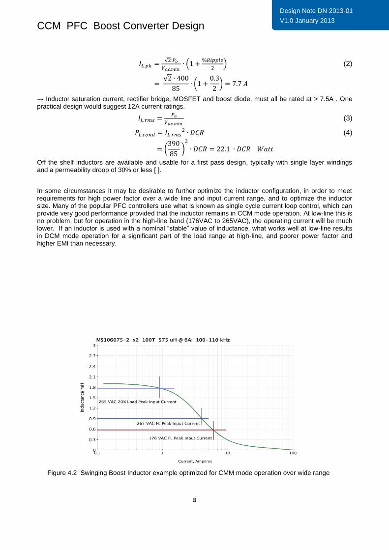
In some circumstances it may be desirable to further optimize the inductor configuration, in order to meet requirements for high power factor over a wide line and input current range, and to optimize the inductor size. Many of the popular PFC controllers use what is known as single cycle current loop control, which can provide very good performance provided that the inductor remains in CCM mode operation. At low-line this is no problem, but for operation in the high-line band (176VAC to 265VAC), the operating current will be much lower. If an inductor is used with a nominal “stable” value of inductance, what works well at low-line results in DCM mode operation for a significant part of the load range at high-line, and poorer power factor and higher EMI than necessary.
Figure 4.2 Swinging Boost Inductor example optimized for CMM mode operation over wide range
CCM PFC Boost Converter Design
9
Design Note DN 2013-01
V1.0 January 2013
A swinging choke design can address this, by using a medium permeability core (75-125μ) of core types such as Arnold/Micrometals Sendust and Magnetics Inc. Kool Mu, of the right energy capability and designing for full load permeability droop by 75-80%, so that with lighter load the inductance swings up. The full details of this technique are beyond the scope of this design note, but it can be facilitated with available design tools from core manufacturers [2]. An example of this with operating current points referenced key line voltage points in one design example is shown in Figure 4.2.
Rectifier Bridge
The bridge total power loss is calculated using the average input current flowing through two of the bridge rectifying diodes.
(5)
Recommendation: GBJ1006-BP. Using a higher rated current bridge can reduce the forward VF, lowering the total power dissipation at a small incremental cost. This is often a sound strategy, as with modern components, the bridge rectifier usually has the highest total semiconductor loss for the PFC stage.
MOSFET
In order to select the the optimum MOSFET, one must understand the MOSFET requirements in a CCM boost converter. High voltage MOSFETS have several families based on different technologies, which each target a specific application, topology or operation. For a boost converter, the following are some major MOSFET selection considerations:
Low FOMs - Ron*Qg and Ron*Eoss
Fast Turn-on/off switching, gate plateau near middle of gate drive range (which balances turn-on and turn-off losses)
Low Output capacitance Coss for low switching energy, to increase light load efficiency- this relates to the Ron*Eoss metric.
Switching and conduction losses must be balanced for minimum total loss - this is typically optimized at the low line condition (if best thermals area desired), where worse case losses and temperature rise occur. In other cases, it may be desired to optimize efficiency at a mid load condition, and ensure that the thermal design is adequate for the worst case low-line dissipation. This varies with overall system targets.
VDS rating to handle spikes/overshoots
Low thermal resistance RthJC. Package selection must consider the resulting total thermal resistance from junction to ambient, and the worst case surge dissipation- this is typically under low-line cycle skip and recovery into highline while ramping the bulk voltage back up.
Body diode speed and reverse recovery charge are not important, since body diode never conducts in a boost converter.
CCM PFC Boost Converter Design
10
Design Note DN 2013-01
V1.0 January 2013
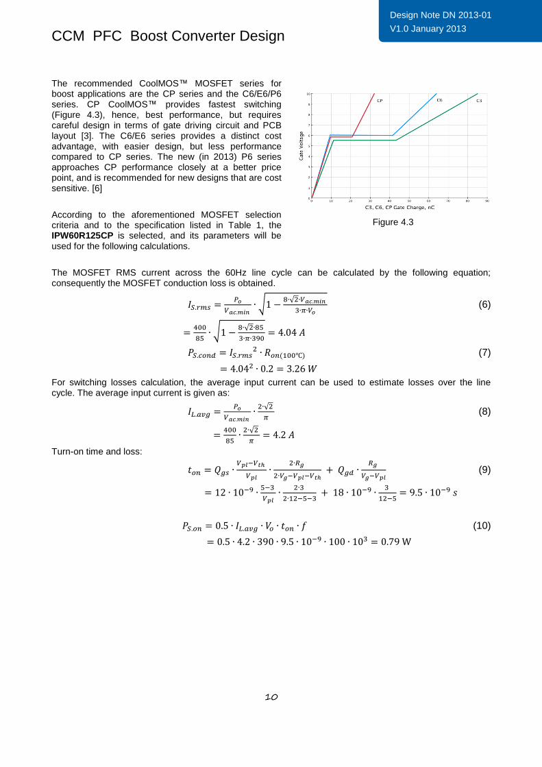
The recommended CoolMOS™ MOSFET series for boost applications are the CP series and the C6/E6/P6 series. CP CoolMOS™ provides fastest switching (Figure 4.3), hence, best performance, but requires careful design in terms of gate driving circuit and PCB layout [3]. The C6/E6 series provides a distinct cost advantage, with easier design, but less performance compared to CP series. The new (in 2013) P6 series approaches CP performance closely at a better price point, and is recommended for new designs that are cost sensitive. [6]
According to the aforementioned MOSFET selection criteria and to the specification listed in Table 1, the IPW60R125CP is selected, and its parameters will be used for the following calculations.
The MOSFET RMS current across the 60Hz line cycle can be calculated by the following equation; consequently the MOSFET conduction loss is obtained.
(6)
(7)
For switching losses calculation, the average input current can be used to estimate losses over the line cycle. The average input current is given as:
(8)
Turn-on time and loss:
(9)
(10)
Figure 4.3
CCM PFC Boost Converter Design
11
Design Note DN 2013-01
V1.0 January 2013
Turn-off time and loss:
(11)
(12)
This is the “classic” format for calculating turn-off time and loss; due to the high Qoss of SJ MOSFETs, the Coss acts like a nonlinear capacitive snubber, and actual turn-off losses with fast switching can be up to 50% lower than calculated. The current flow through the drain during turn-off under these conditions is non-dissipative capacitive current, and with fast drive, the channel may be completely turned off by the onset of drain voltage rise.
Output capacitance Coss switching loss:
(13)
Gate drive loss:
(14)
Boost Diode
Selection of the boost diode is a major design decision in CCM boost, since the diode is hard commutated at a high current, and reverse recovery can cause significant power loss, noise and current spikes. Reverse recovery can be a bottle neck for high switching frequency and high power density power supplies. Additionally, at low line, the available diode conduction duty cycle is quite low, and the forward current quite high in proportion to the average current. For that reason, the first criteria for selecting a diode in CCM boost are fast recovery with low reverse recovery charge, followed by VF operating at high forward current.
CCM PFC Boost Converter Design
12
Design Note DN 2013-01
V1.0 January 2013
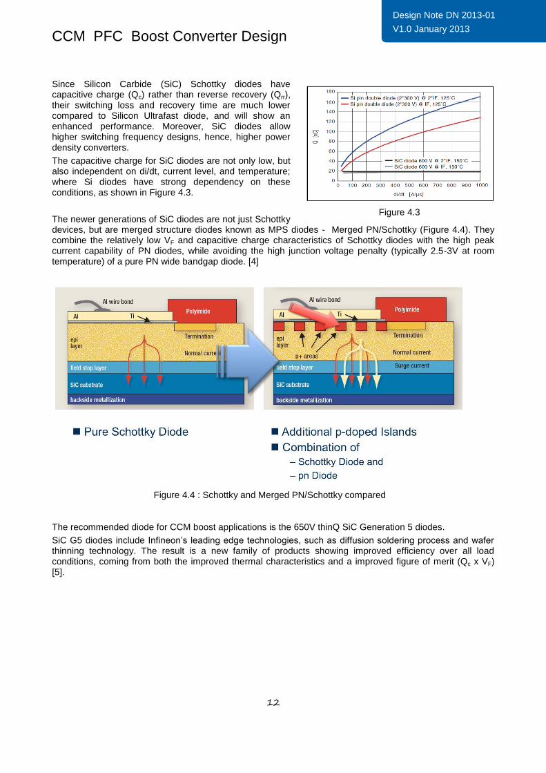
Since Silicon Carbide (SiC) Schottky diodes have capacitive charge (Qc) rather than reverse recovery (Qrr), their switching loss and recovery time are much lower compared to Silicon Ultrafast diode, and will show an enhanced performance. Moreover, SiC diodes allow higher switching frequency designs, hence, higher power density converters.
The capacitive charge for SiC diodes are not only low, but also independent on di/dt, current level, and temperature; where Si diodes have strong dependency on these conditions, as shown in Figure 4.3.
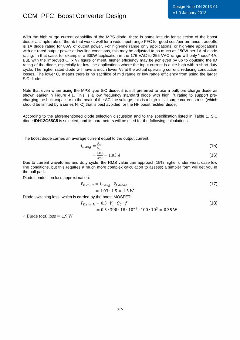
The newer generations of SiC diodes are not just Schottky devices, but are merged structure diodes known as MPS diodes - Merged PN/Schottky (Figure 4.4). They combine the relatively low VF and capacitive charge characteristics of Schottky diodes with the high peak current capability of PN diodes, while avoiding the high junction voltage penalty (typically 2.5-3V at room temperature) of a pure PN wide bandgap diode. [4]
The recommended diode for CCM boost applications is the 650V thinQ SiC Generation 5 diodes.
SiC G5 diodes include Infineon’s leading edge technologies, such as diffusion soldering process and wafer thinning technology. The result is a new family of products showing improved efficiency over all load conditions, coming from both the improved thermal characteristics and a improved figure of merit (Qc x VF) [5].
Figure 4.3
Figure 4.4 : Schottky and Merged PN/Schottky compared
CCM PFC Boost Converter Design
13
Design Note DN 2013-01
V1.0 January 2013
With the high surge current capability of the MPS diode, there is some latitude for selection of the boost diode- a simple rule of thumb that works well for a wide input range PFC for good cost/performance tradeoffs is 1A diode rating for 80W of output power. For high-line range only applications, or high-line applications with de-rated output power at low-line conditions, this may be adjusted to as much as 150W per 1A of diode rating. In that case, for example, a 600W application in the 176 VAC to 255 VAC range will only “need” 4A. But, with the improved Qc x VF figure of merit, higher efficiency may be achieved by up to doubling the ID rating of the diode, especially for low-line applications where the input current is quite high with a short duty cycle. The higher rated diode will have a much lower VF at the actual operating current, reducing conduction losses. The lower Qc means there is no sacrifice of mid range or low range efficiency from using the larger SiC diode.
Note that even when using the MPS type SiC diode, it is still preferred to use a bulk pre-charge diode as shown earlier in Figure 4.1. This is a low frequency standard diode with high I
2t rating to support pre-
charging the bulk capacitor to the peak of the AC line voltage; this is a high initial surge current stress (which should be limited by a series NTC) that is best avoided for the HF boost rectifier diode.
According to the aforementioned diode selection discussion and to the specification listed in Table 1, SiC diode IDH12G65C5 is selected, and its parameters will be used for the following calculations.
The boost diode carries an average current equal to the output current.
(15)
(16)
Due to current waveforms and duty cycle, the RMS value can approach 15% higher under worst case low line conditions, but this requires a much more complex calculation to assess; a simpler form will get you in the ball park.
Diode conduction loss approximation:
(17)
Diode switching loss, which is carried by the boost MOSFET:
(18)
CCM PFC Boost Converter Design
14
Design Note DN 2013-01
V1.0 January 2013
Output Capacitor
The output capacitor is sized to meet the hold-up time and voltage ripple requirements, the capacitor is selected to have the larger value of the two equations below.
(19)
(20)
→
The capacitor RMS current across the 60Hz line cycle can be calculated by the following equation, consequently the capacitor ESR loss is obtained.
(21)
(22)
Recommendation: 2 parallel EET-UQ2S331KF
CCM PFC Boost Converter Design
15
Design Note DN 2013-01
V1.0 January 2013
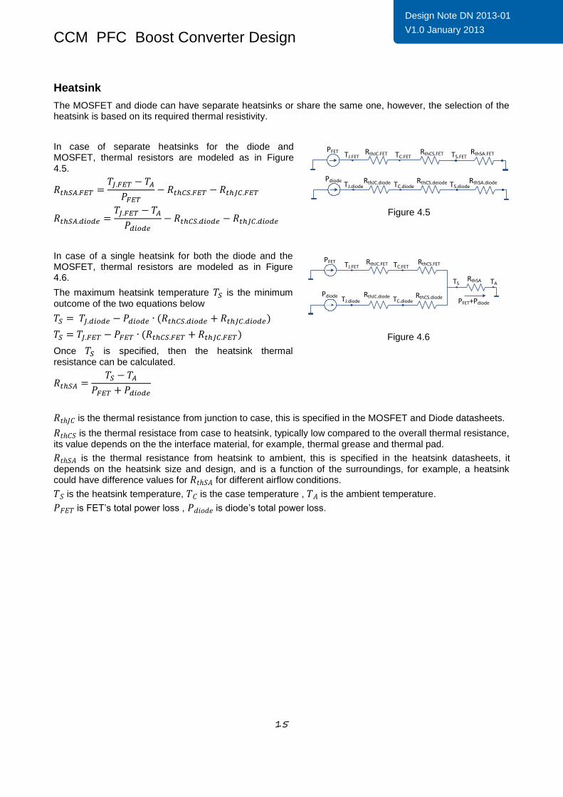
Heatsink
The MOSFET and diode can have separate heatsinks or share the same one, however, the selection of the heatsink is based on its required thermal resistivity.
In case of separate heatsinks for the diode and MOSFET, thermal resistors are modeled as in Figure 4.5.
In case of a single heatsink for both the diode and the MOSFET, thermal resistors are modeled as in Figure 4.6.
The maximum heatsink temperature is the minimum
outcome of the two equations below
Once is specified, then the heatsink thermal resistance can be calculated.
is the thermal resistance from junction to case, this is specified in the MOSFET and Diode datasheets.
is the thermal resistace from case to heatsink, typically low compared to the overall thermal resistance, its value depends on the the interface material, for example, thermal grease and thermal pad.
is the thermal resistance from heatsink to ambient, this is specified in the heatsink datasheets, it depends on the heatsink size and design, and is a function of the surroundings, for example, a heatsink could have difference values for for different airflow conditions.
is the heatsink temperature, is the case temperature , is the ambient temperature.
is FET’s total power loss , is diode’s total power loss.
Figure 4.5
PFET RthJC.FET RthCS.FET
RthJC.diode RthCS.diode
RthSA
TJ.FET
TJ.diode
TS TA
TC.FET
TC.diodePdiode
PFET+Pdiode
Figure 4.6
PFET RthJC.FET RthCS.FET RthSA.FET
TJ.FET TS.FETTC.FET
Pdiode RthJC.diode RthCS.deiode RthSA.diode
TJ.diode TS.diodeTC.diode
CCM PFC Boost Converter Design
16
Design Note DN 2013-01
V1.0 January 2013
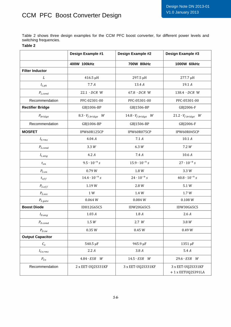
Table 2 shows three design examples for the CCM PFC boost converter, for different power levels and switching frequencies.
Table 2
Design Example #1 Design Example #2 Design Example #3
400W 100kHz 700W 80kHz 1000W 60kHz
Filter Inductor
Recommendation PFC-02301-00 PFC-05301-00 PFC-05301-00
Rectifier Bridge GBJ1006-BP GBJ1506-BP GBJ2006-F
Recommendation GBJ1006-BP GBJ1506-BP GBJ2006-F
MOSFET IPW60R125CP IPW60R075CP IPW60R045CP
Boost Diode IDH12G65C5 IDW20G65C5 IDW30G65C5
Output Capacitor
Recommendation 2 x EET-UQ2S331KF 3 x EET-UQ2S331KF 3 x EET-UQ2S331KF
+ 1 x EETUQ2S391LA
CCM PFC Boost Converter Design
17
Design Note DN 2013-01
V1.0 January 2013
5 References
[1] Precision, Inc., Vertical Mount toroidal inductors.
http://www.precision-inc.com/power-factor-correction-inductor-vertical-mount-toroid-p-691-l-en.html
[2] Micrometals Arnold Powder Core Inductor Design Software.
http://www.micrometalsarnoldpowdercores.com/software.php
[3] F. Bjoerk, J. Hancock, G. Deboy, Infineon Technologies Application Note: “CoolMOS CP - How to make most beneficial use of the latest generation of super junction technology devices”. February 2007. http://www.infineon.com/dgdl/Aplication+Note+CoolMOS+CP+(+AN_CoolMOS_CP_01_Rev.+1.2).pdf?folderId=db3a304412b407950112b408e8c90004&fileId=db3a304412b407950112b40ac9a40688
[4] R. Rupp, J. Hancock, F. Bjoerk, M. Treu, “Silicon Carbide Merged PN/Schottky Diodes for PFC Applications”, Infineon Technologies NA, V. 1.2, 2008; upon request.
[5] Product Brief, 650V SiC thinQ!™ Generation 5 diodes.
http://www.infineon.com/dgdl/Infineon+-+Product+Brief+-+650V+SiC+Generation+5+diodes.pdf?folderId=db3a304314dca38901152836c5a412ab&fileId=db3a3043399628450139b06e16a721d0
[6] CoolMOSTM
Selection Guide.
http://www.infineon.com/dgdl/infineon_CoolMOS_Selection-Guide.pdf?folderId=db3a304314dca389011528372fbb12ac&fileId=db3a30432f91014f012f95fc7c24399d
CCM PFC Boost Converter Design
18
Design Note DN 2013-01
V1.0 January 2013
Symbols used in formulas
Vac.min: Minimum input voltage Vo: Output voltage Vac.min: Minimum input voltage Vo: Output voltage Po: Output power f: Switching frequency T: Switching time period fline: line frequency L: Filter inductor %Ripple: Inductor current ripple percentage to input current DCR: Inductor DC resistance IL.avg: Inductor average current across the line cycle IL.pk: Inductor peak current PL.cond: Inductor conduction loss VF.bridge: Bridge diode forward voltage drop Pbridge: Bridge power loss Ron(100C): MOSFET on resistance at 100
oC
Qgs: MOSFET gate-source charge Qgd: MOSFET gate-drain charge Qg: MOSFET total gate charge Rg: MOSFET gate resistance Vpl: MOSFET gate plateau voltage Vth: MOSFET gate threshold voltage ton: MOSFET switching on time toff: MOSFET switching off time Eoss: MOSFET output capacitance switching energy IS.rms: MOSFET rms current across the line cycle PS.cond: MOSFET conduction loss PS.on: MOSFET switching on power loss PS.off: MOSFET switching off power loss PS.oss: MOSFET output capacitance switching loss PS.gate: MOSFET gate drive loss ID.avg: Boost diode average current VF.diode: Boost diode forward voltage drop Qrr: Boost diode reverse recovery charge PDcond: Boost diode conduction loss PD.sw: Boost diode switching loss Co: Output capacitor ESR: Output capacitor resistance thold: Hold-up time Vo.min: Hold up minimum output voltage ∆Vo: Output voltage ripple ICo.rms: Output capacitor rms current PCo: Output capacitor conduction loss