Embed Size (px)
Citation preview

4/18/2016
1
Recent Advances and New Trends in
Semiconductor Packaging
by
John H Lau [email protected]
TI Auditorium, April 12, 2016 1
IEEE/CMPT Society Lecture in the Santa Clara Valley
PURPOSES To present the recent advances and new trends
in the following semiconductor packaging technologies:
Fan-Out Wafer/Panel-Level Packaging
3D IC Integration with TSVs
2.5D IC Integration/TSV-less Interposers
2

4/18/2016
2
Fan-Out Wafer/Panel-Level Packaging
(1) PATENTS IMPACTING THE SEMICONDUCTOR PACKAGING
(2) FAN-OUT WAFER/PANEL-LEVEL PACKAGING FORMATIONS (A) Chip-First (Die-Down) (B) Chip-First (Die-Up) (C) Chip-Last (RDL-First)
(3) RDL FABRICATIONS (A) Polymer Method (B) PCB/LDI Method (C) Cu Damascene Method
(4) TSMC InFO-WLP and InFO-PoP vs. Samsung ePoP (5) WAFER vs. PANEL CARRIER (6) NOTES ON DIRECTRIC AND EPOXY MOLD COMPOUND (7) SEMICONDUCTOR and PACKAGING FOR IoTs (SiP) (8) WAFER-LEVEL SYSTEM-in-PACKAGE (WLSiP) (9) PACKAGE-FREE LED (EMBEDDED LED CSP) (10) SUMMARY
3
Typical PCB Assemblies in Electronic Products
Printed Circuit Board
IC Chip B Package
Substrate Solder Joint
Lead-frame Solder Joint
Au/Cu wire Underfill
Solder Bump Molding Compound
IC Chip A
Cu Trace
Via
Lau, ECTC-PDC-2005 4

4/18/2016
3
Patents Impacting the Semiconductor Packaging
(Even there are many important patents such as flip chip and TSV, however I think the following 4 impact the semiconductor packaging the most.)
Lead-Frame Organic Substrate with Solder Balls Fan-In Wafer Level Packaging Fan-Out Wafer Level Packaging
5
The first lead-frame patent! Lau, CSR, 19(6), 2015
6

4/18/2016
4
Chip Circuitry Fan-Out by Lead-Frame Silicon Chip
Gold Wires
Silicon Chip
Gull-wing Lead
Chip Circuitry is Fanned-Out by Lead-Frame to PCB.
PCB
J- Lead
Lead-Frame
Lau, CSR, 19(6), 2015 7
Lead-Frame is replaced by package substrate and solder balls to fan-out the chip circuitry to PCB. Lau, CSR, 19(6), 2015
8

4/18/2016
5
Chip: 4 to 625mm2 Solder ball: ranging from 10s to 1000s Pitch: ranging from 0.5, 0.65, 0.8, 1, to 1.27mm PBGA package size: range from 10mmx10mm, to as large as 55mmx55mm
Chip
Wire bond
Package Substrate
Over Mold
Printed Circuit Board
Die Attach
Solder Joint
Printed Circuit Board
Chip
Solder Joint Solder bump
Package Substrate
Underfill Chip face down (flip chip)
The circuitry of Chip is Fan-Out Through Substrate and Solder Balls
1993, AMKOR led OSATs to license this technology
from Motorola.
BGA (ball grid array) era began!
Lau, CSR, 19(6), 2015 9
Fan-in WLP (WLCSP) to eliminate package substrate and underfill. Lau, CSR, 19(6), 2015
10

4/18/2016
6
Wafer-Level Chip Size Packages (WLCSP) In the past 15 years, WLCSP has been used mainly for low pin-counts (≤ 200) with pitch ranges from 0.5, 0.4, 0.35, and 0.3mm, small die size (≤ 6mm x 6mm), low-cost, low-end, low-profile, and high-volume applications. Semiconductor ICs such as the electrostatic discharge / electromagnetic interference protection, radio frequency (RF) filtering, power management, power amplifiers, surface acoustic wave / bulk acoustic wave filters, DC/DC converters, light-emitting diodes, battery and display driver, audio/video codecs and amplifiers, logic gates, electrically erasable programmable read-only memory (EEPROM), microcontrollers, Bluetooth + frequency modulation (FM) + Wi-Fi combos, global positioning system (GPS), baseband, and radio frequency transceivers have been packaged with various WLCSPs for various electronic products such as cell-phones, smartphones and tablets, and wearables. For internet of things (IoTs), the CMOS image sensors and MEMS sensors will also be packaged with WLCSPs.
Chip 2001, AMKOR led OSATs and Foundries to license this technology from Flip Chip
Technologies.
WLP (wafer-level packaging) era began!
Lau, CSR, 19(6), 2015 11
Metal wire (RDL)
Metal pad
Over Mold Encapsulant
Dielectric
Solder Ball
PCB
Solder Mask (Polyimide)
CHIP
Chip Edge
RDLs to fan-out the circuitry beyond the chip edges without using a lead-frame or substrate.
Lau, CSR, 19(6), 2015 12

4/18/2016
7
26a 36a
22 34c
40
f
14b
36a
(Chip)
(Chip Edge)
Fan-Out Wafer-Level Packaging
RDLs to fan-out the circuitry beyond the chip edges.
(RDL)
Lau, CSR, 19(6), 2015 13
Infineon’s US 6,727,576
Lau, CSR, 19(6), 2015 14

4/18/2016
8
Advantages of Fan-Out Wafer/Panel Level Packaging over FCPBGA
Chip
Organic Substrate Underfill
Solder Bumps Solder Balls
Molded Compound
(1) lower cost (2) lower profile (3) eliminating the substrate (4) eliminating the wafer bumping (5) eliminating the flip chip reflow (6) eliminating the flux cleaning (7) eliminating the underfill (8) better electrical performance (9) better thermal performance (10) easier to go for system-in-package (SiP) and 3D IC packaging
Chip Mold
Compound
Lau, CSR, 19(6), 2015 15
(1) the use of known good die (KGD) (2) better wafer-level yield (3) using the best of silicon (4) multichip (5) embedded integrated passive devices (6) more than one RDL (7) higher pin counts (or die shrink) (8) better thermal performance (9) easier to go for SiP and 3D IC packaging (10) higher PCB level reliability.
Chip Mold
Compound
Advantages of Fan-Out Wafer/Panel Level Packaging over Fan-In Wafer Level Packaging
Chip
Lau, CSR, 19(6), 2015 16

4/18/2016
9
Chip-First (Die-Up) Chip-First (Die-Down)
Most of the fan-out wafer/panel-level
packages in manufacturing today use either one of these formations for portable, mobile,
and wearable products.
The reconfigured carrier is neither wafer or panel!
Lau, et al., CSR 20(3), 2016 17
Temporary (wafer or panel) carrier
2-side (thermal release ) tape
KGDKGDKDG
Remove carrier and tape
Dice the molded wafer or panel into individual packages
Die face-down
Over mold the reconfigured
carrier
Test for KGD and Dice
Passivation
Device Wafer
CHIPCHIPKGDRDLs
Solder balls
Al or Cu Pad
CHIP
Build RDLs and mount solder balls
RDLsSolder balls
CHIPCHIPKGD CHIPCHIPKGDEMC
EMC (epoxy mold compound)
FOW/PLP Formation: Chip-First (Die-Down)
Lau, et al., CSR 20(3), 2016 18

4/18/2016
10
Lau, et al., CSR 20(3), 2016 19
TSMC’s InFO (Integrated Fan-Out) WLP for Apple’s
A10 Application Processor Chip-Frist (Die-Up)
Lau, et al., CSR 20(3), 2016 20
4/18/2016
11
US 9,000,584 B2 (Publication Date: April 7, 2015) PACKAGED SEMICONDUCTOR DEVICE WITH A MOLDING COMPOUND AND A
METHOD OF FORMING THE SAME Jing-Cheng Lin, Hsinchu County (TW); Jui-Pin Hung, Hsinchu (TW); Nai-Wei Liu, Fengshan (TW); Yi-Chao
Mao, Zhongli (TW); Wan-Ting Shih, Touwu Township (TW); and Tsan-Hua Tung, Hsinchu (TW) Assigned to Taiwan Semiconductor Manufacturing Company, Ltd., (TW)
FIG. 1I also shows a more detailed view of the die 104 and the wiring layer 108, in accordance with some embodiments. The view of the die 104 and wiring layer 108 are exemplary; alternatively, the die 104 and wiring layer 108 may comprise other configurations, layouts and/or designs. In the embodiment shown, the die 104 includes a substrate 124 comprising silicon or other semiconductive materials. Insulating layers 126 a and 126 b may comprise passivation layers disposed on the substrate 124. Contact pads 128 of the die 104 may be formed over conductive features of the substrate such as metal pads 127, plugs, vias, or conductive lines to make electrical contact with electrical components of the substrate 124, which are not shown.
Lau, CSR, 19(6), 2015 21
Temporary (wafer or panel) carrier 2-side tape
KGD KGD KGD
Build RDLs on contact pads and
mount solder balls
Solder balls RDLs
Remove carrier and tape and then dice the molded wafer or panel into individual packages
Die face-up
Test for KGD
Device Wafer
RDLs Solder balls
CHIP
Passivation
UBM
Al or Cu Pad
Contact pad
KGD KGD KGD
Passivation
UBM
Al or Cu Pad
Contact pad
CHIP
Polymer
Over mold the reconfigured
carrier
EMC
Backgrind the over-mold to expose the contact pad
Sputter UBM and electroplate contact pad
Spin coat a polymer and dice the wafer
FOW/PLP Formation: Chip-First (Die-Up)
Lau, et al., CSR 20(3), 2016 22

4/18/2016
12
Forecast Fan-Out Wafer-Level Packaging (FOWLP) Revenues ($M)
Jan, 2016
23
Key Components in iPhone 6 Plus
2GB LPDDR4
A9 application processor fabricated by 14/16nm Fin-FET process technology
Package Substrate for LPDDR4
iPhone 6S/6S Plus
A9
LPDDR4 3-layer Coreless substrate
A9
2-2-2 build-up
substrate
150µm-pitch staggered C4 bumps
90µm
Wirebond
Wirebond
3-layer Coreless
2-2-2 Build-up Package Substrate for A9 processor
Lau, CSR, 19(6), 2015 24

4/18/2016
13
TSMC’s InFO_PoP Conventional PoP for
Application Processor (AP) chipset
Eliminated wafer bumping, solder reflow, flux cleaning, underfilling,
and package substrate. Lower Profile!
TSMC’s PoP for Application Processor (AP)
chipset
TMV
TIV
AP AP
TSMC SEMIEURO, 2014
Lau, CSR, 19(6), 2015 25
Samsung’s ePoP
26
4/18/2016
14
10-layer PCB
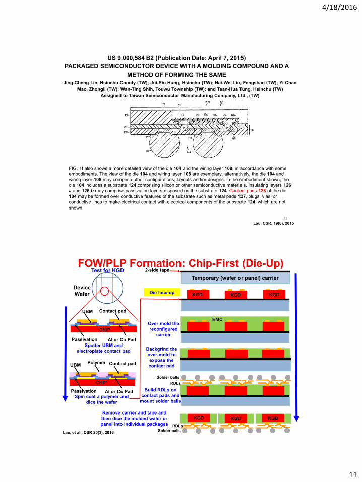
Wire bonding Nand Flash chips
Molding Coreless Substrate
SK Hynix’s MLC (Multi Level Cell) 128Gb (Gigabit) or 8GB (Gigabyte) NAND Flash in iPhone
FBGA (Fine-pitch Ball Grid Array)
27
Exynos 7 Octa
On February 17, 2015, Samsung announced that their Exynos 7 Octa application processor (AP) has been in production using their 14nm FinFET technology process (the first in the world for AP.)
Package substrate
Package substrate
ePoP
PCB
Samsung’s Application Processor Chip-Set and Memory chip-Set
28

4/18/2016
15
Exynos AP
ePoP (Flash and LPDDR4
combination)
Conventional Solution
Samsung’s Next Generation High-End Smartphones
A 40% saving!
ePoP Solution ePoP
PCB
NAND Controller
4@64Gb MLC flash 4@6Gb LPDDR4
Exynos AP
PCB
eMMC Flash
29
Embedded Fan-Out Panel Wafer-Level Packaging
(FOPLP)
30

4/18/2016
16
Wafer vs. Panel
(610mm x 457mm) Area > 3.8 X 12”-wafer
12” wafer carrier
24”x18” carrier
Lau, CSR, 19(6), 2015 31
For fan-out wafer/panel packaging, why use panel leads to lower cost?
Because the RDLs of the panel are fabricated by
PCB/LDI technology and P&P of dies and passives are by SMT equipment.
Since the area of panel is larger than that of wafer, thus more packages can be made. It should be noted that, fan-out panel wafer level packaging is applied to low-end, low-performance, low pin-count, and small devices. The line width/spacing of the RDLs are >10µm.
Lau, CSR, 19(6), 2015 32

4/18/2016
17
IZM Fan-Out Panel-Level Packaging Integration line
IZM ECTC 2015 33
Lau, et al., CSR 20(3), 2016 34

4/18/2016
18
> 10µm
< 2 - 5µm
5 - 10µm
Reconfigured carrier width/spacing Appl.
Middle-end
High-end
Low-end
thick.
≤ 2µm
≥ 3µm
≥ 5µm
Laser direct
imaging
Stepper
Mask aligner or Stepper
_Cu damascene _Semi. Equip. _High-Precision P&P
_Cu plating _Packaging Equip. _Ordinary P&P
_PCB Cu plating _PCB Equip. _SMT P&P
Litho.
Proc./Equip. Dielectric Mat.(Thick.)
SiO2 (1µm)
Polymers (4 - 8µm)
Resin (15 - 30µm)
Redistribution Layer
KGD KGD EMC
RDLs Pad
Pad
Solder mask, polymer, or SiO2
Dielectric
Solder ball
The geometry, material, process, equipment, and application of fan-out wafer/panel-level packaging
Lau, CSR, 19(6), 2015 35
Chip-Last (RDL-First)
For very high-density and high-performance
applications, e.g., high-end servers, computers, and networking.
The reconfigured carrier is wafer!
Lau, et al., CSR 20(3), 2016 36

4/18/2016
19
Chip-Last (RDL-First) Fan-Out Wafer-Level Packaging (FOWLP)
Since 2006, NEC Electronics Corporation (now Renesas Electronics Corporation) has been developing a novel SMAFTI (SMArt chip connection with FeedThrough Interposer) packaging technology for:
inter-chip wide-band data transfer 3D stacked memory integrated on a logic devices system in wafer-level package (SiWLP) (2010) and “RDL-first” fan-out wafer-level packaging (2011)
The FTI (feedthrough interposer) of SMAFTI is a film with ultra-fine line width and spacing RDLs. The dielectric of the FTI is usually SiO2 or polymer and the conductor wiring of the RDLs is Cu. The FTI not only supports the RDLs underneath within the chip, it also supports beyond the edges of the chip. Area array solder balls are mounted at the bottom-side of the FTI which are to be connected to the PCB. Epoxy mold compound (EMC) is used to embed the chip and support the RDLs and solder balls. In 2015, Amkor announced a very similar technology called “SWIFTTM” (silicon wafer integrated fan-out technology). Lau, et al., CSR 20(3), 2016
37
A 3D Stacked Memory Integrated on a Logic Device Using SMAFTI Technology
Yoichiro Kurita, Satoshi Matsui, Nobuaki Takahashi, Koji Soejima, Masahiro Komuro, Makoto Itou, Chika Kakegawa, Masaya Kawano, Yoshimi Egawa, Yoshihiro Saeki, Hidekazu Kikuchi, Osamu Kato, Azusa Yanagisawa,
Toshiro Mitsuhashi, Masakazu Ishino, Kayoko Shibata, Shiro Uchiyama, Junji Yamada, and Hiroaki Ikeda NEC Electronics, Oki Electric Industry, and Elpida Memory
1120 Shimokuzawa, Sagamihara, Kanagawa 229-1198, Japan
NEC ECTC2007 38
4/18/2016
20
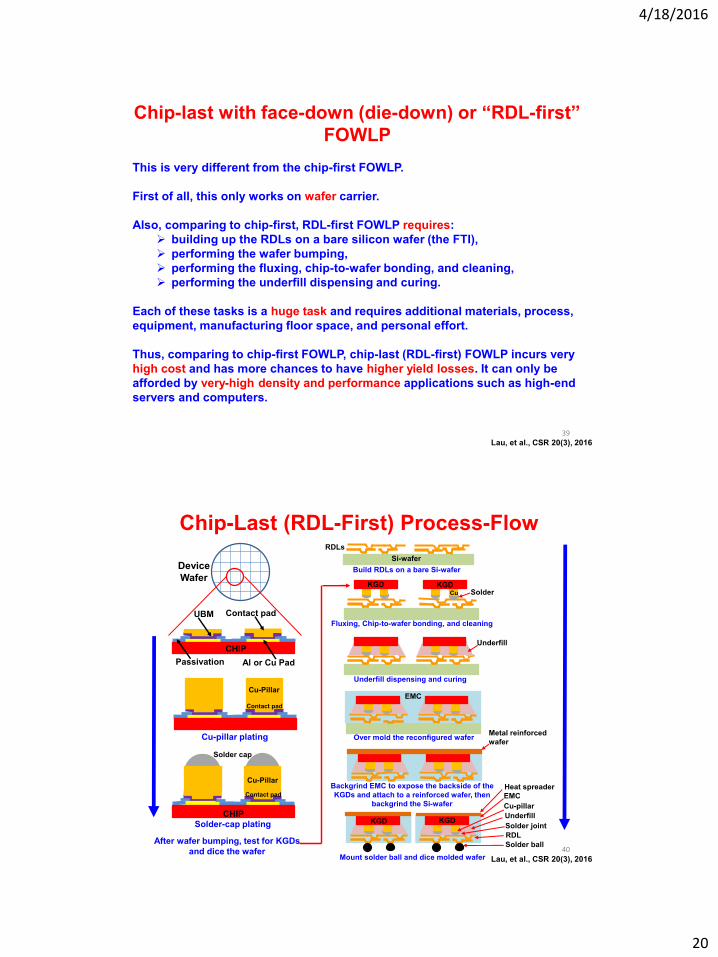
Chip-last with face-down (die-down) or “RDL-first” FOWLP
This is very different from the chip-first FOWLP. First of all, this only works on wafer carrier. Also, comparing to chip-first, RDL-first FOWLP requires:
building up the RDLs on a bare silicon wafer (the FTI), performing the wafer bumping, performing the fluxing, chip-to-wafer bonding, and cleaning, performing the underfill dispensing and curing.
Each of these tasks is a huge task and requires additional materials, process, equipment, manufacturing floor space, and personal effort. Thus, comparing to chip-first FOWLP, chip-last (RDL-first) FOWLP incurs very high cost and has more chances to have higher yield losses. It can only be afforded by very-high density and performance applications such as high-end servers and computers.
Lau, et al., CSR 20(3), 2016 39
Chip-Last (RDL-First) Process-Flow
Build RDLs on a bare Si-wafer
RDLs
Device Wafer
After wafer bumping, test for KGDs and dice the wafer
CHIPPassivation
UBM
Al or Cu Pad
Contact pad
Cu-pillar plating
Cu-Pillar
Solder-cap plating
Solder cap
Cu-Pillar
Contact pad
Contact pad
CHIP
Mount solder ball and dice molded wafer
Fluxing, Chip-to-wafer bonding, and cleaning
Underfill dispensing and curing
Backgrind EMC to expose the backside of the KGDs and attach to a reinforced wafer, then
backgrind the Si-wafer
KGD KGD
Underfill
Over mold the reconfigured wafer
EMC
RDLSolder ball
Solder joint
Cu-pillarUnderfill
EMC
KGDKGD
Cu Solder
Metal reinforced wafer
Heat spreader
Si-wafer
Lau, et al., CSR 20(3), 2016 40
4/18/2016
21
Passivation pad
Cu
(1) Redef. Passivation
(2) Sputter Ti/Cu (4) Patterning
(3) Spin Resist
Mask Ti
UV
Solder Cu
(5) ECD Cu, Solder
(6) Strip Resist
(7) Etch Cu/Ti
(8) Flux, Reflow
Cu Solder
(5) ECD Cu, Solder
(6) Strip Resist
(7) Etch Cu/Ti
(8) Flux, Reflow
Solder
Solder
Cu Cu
Solder
Si
Si
Solder
Passivation
Passivation
C4 (controlled collapsed chip connection) bump
C2 (chip connection) bump
TiCu
TiCu
Pad
Pad
Cu
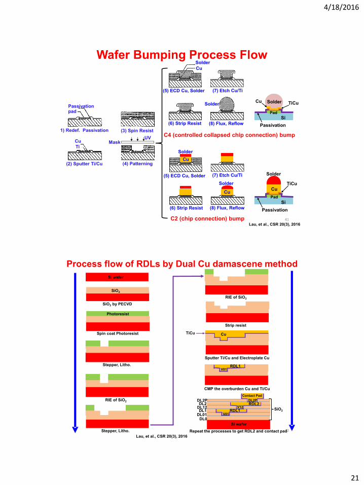
Wafer Bumping Process Flow
Lau, et al., CSR 20(3), 2016 41
Process flow of RDLs by Dual Cu damascene method Si wafer
SiO by PECVD
SiO 2
2
Spin coat Photoresist
Stepper, Litho.
Stepper, Litho.
RIE of SiO2
Photoresist
RIE of SiO2
Strip resist
Sputter Ti/Cu and Electroplate Cu
CMP the overburden Cu and Ti/Cu
Repeat the processes to get RDL2 and contact pad
RDL1 V01
TiCu
RDL1 V12
V01
Contact Pad
Si wafer
RDL2 SiO2 DL1
DL2
DL0 DL01 DL12 DL2P
Cu
DL2P
Lau, et al., CSR 20(3), 2016 42
4/18/2016
22
V01RDL1
RDL2RDL3
V12
V23
Contact PadUBM
Si wafer
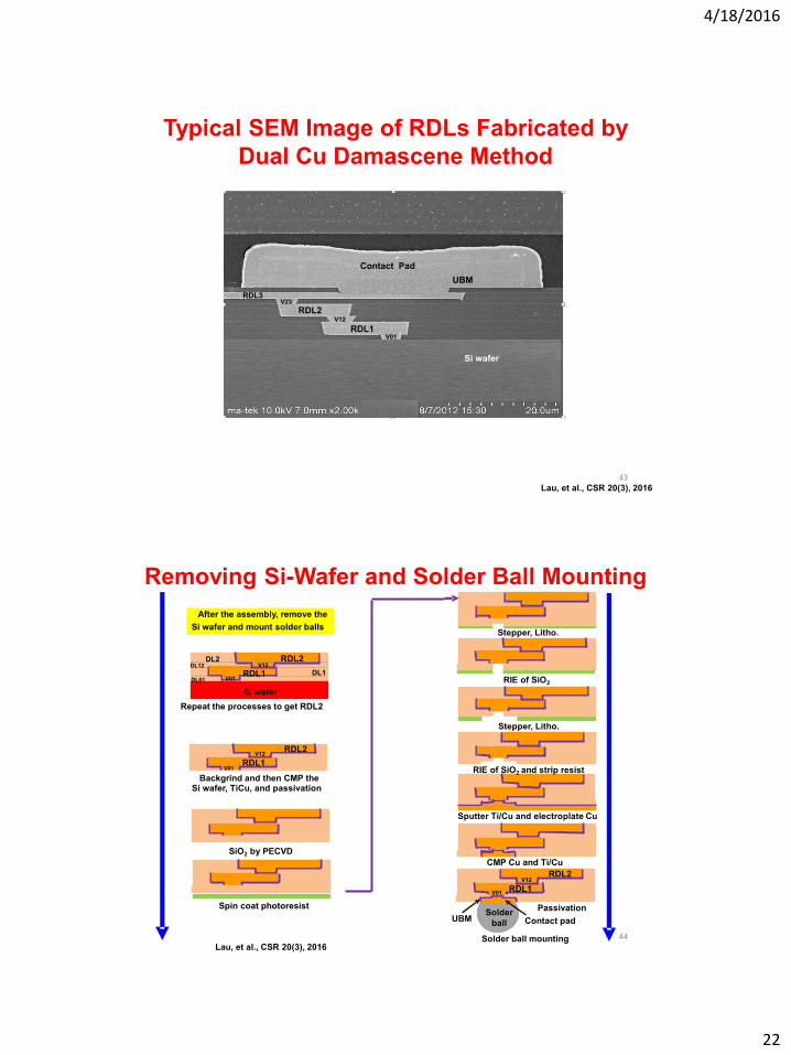
Typical SEM Image of RDLs Fabricated by Dual Cu Damascene Method
Lau, et al., CSR 20(3), 2016 43
Removing Si-Wafer and Solder Ball Mounting
Repeat the processes to get RDL2
Si wafer, TiCu, and passivation
After the assembly, remove the Si wafer and mount solder balls
RDL2 RDL1 V01
V12
Si wafer
DL1
DL2 DL12
DL01
Backgrind and then CMP the
SiO 2 by PECVD
Spin coat photoresist
V01 RDL1
RDL2 V12
Solder ball mounting
CMP Cu and Ti/Cu
Sputter Ti/Cu and electroplate Cu
Stepper, Litho.
RIE of SiO 2
Stepper, Litho.
RIE of SiO 2 and strip resist
RDL2 RDL1
V12
UBM Contact pad Solder
ball Passivation
V01
Lau, et al., CSR 20(3), 2016 44

4/18/2016
23
AMKOR’s SWIFT
R. Huemoeller, and C. Zwenger, “Silicon wafer integrated fan-out technology”, Chip Scale Review, March/April Issue, 2015. 45
AMKOR’s SWIFT (Silicon Wafer Integrated Fan-out Technology)
Conventional Fan-out Technology SWIFT
Cu Solder Cu-pad
46
4/18/2016
24
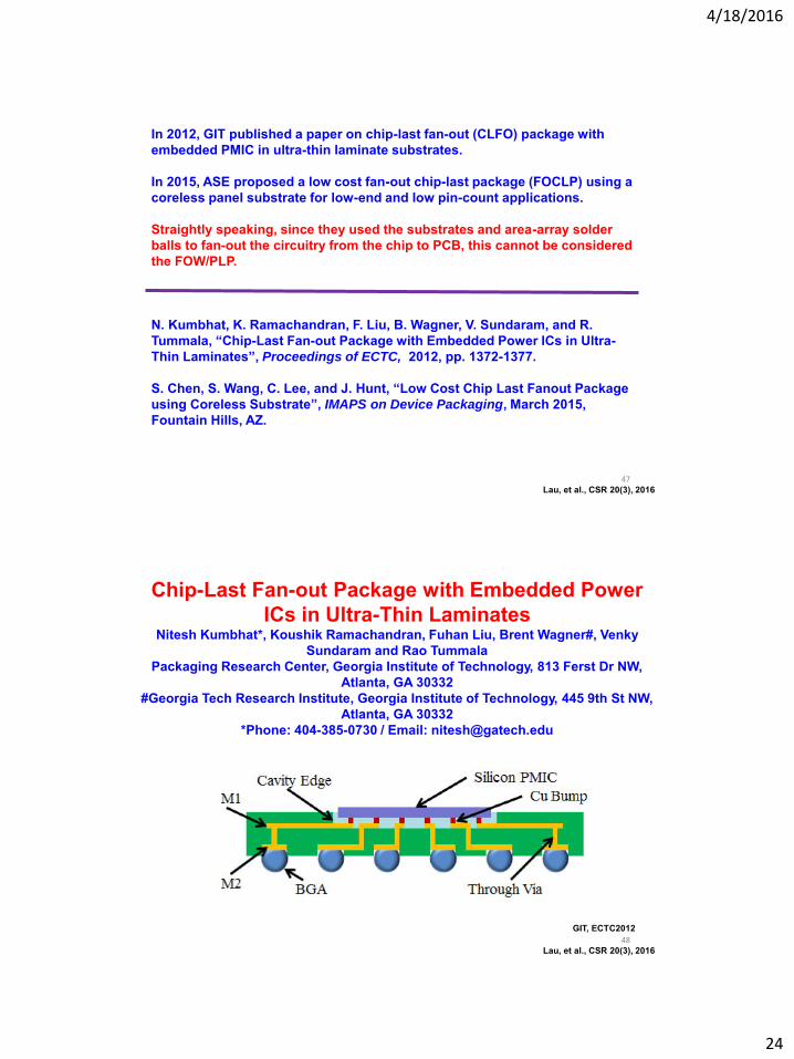
In 2012, GIT published a paper on chip-last fan-out (CLFO) package with embedded PMIC in ultra-thin laminate substrates. In 2015, ASE proposed a low cost fan-out chip-last package (FOCLP) using a coreless panel substrate for low-end and low pin-count applications. Straightly speaking, since they used the substrates and area-array solder balls to fan-out the circuitry from the chip to PCB, this cannot be considered the FOW/PLP. N. Kumbhat, K. Ramachandran, F. Liu, B. Wagner, V. Sundaram, and R. Tummala, “Chip-Last Fan-out Package with Embedded Power ICs in Ultra-Thin Laminates”, Proceedings of ECTC, 2012, pp. 1372-1377. S. Chen, S. Wang, C. Lee, and J. Hunt, “Low Cost Chip Last Fanout Package using Coreless Substrate”, IMAPS on Device Packaging, March 2015, Fountain Hills, AZ.
Lau, et al., CSR 20(3), 2016 47
Chip-Last Fan-out Package with Embedded Power ICs in Ultra-Thin Laminates
Nitesh Kumbhat*, Koushik Ramachandran, Fuhan Liu, Brent Wagner#, Venky Sundaram and Rao Tummala
Packaging Research Center, Georgia Institute of Technology, 813 Ferst Dr NW, Atlanta, GA 30332
#Georgia Tech Research Institute, Georgia Institute of Technology, 445 9th St NW, Atlanta, GA 30332
*Phone: 404-385-0730 / Email: [email protected]
GIT, ECTC2012
Lau, et al., CSR 20(3), 2016 48

4/18/2016
25
Low Cost Chip Last Fanout Package using Coreless Substrate
Scott Chen, Simon Wang, Coltrane Lee, John Hunt
ASE Group, Chung-Li, Taiwan ROC
IMAPS, Mar 2015 Lau, et al., CSR 20(3), 2016
49
NOTES ON DIELECTRIC MATERIALS For the RDLs in Chip-First FOWLP with very fine line width/space, the dielectric layer (SiO2) is fabricated by the low-temperature PECVD (<200oC) or SACVD (sub-atmosphere chemical vapor deposition) (170oC), which are less than the critical temperature (230oC) of the compression molded EMC. For polymer dielectric layer, low curing temperature polymers such as BCB and PBO are required. For example, the curing temperature of DOW’s BCB is 200oC and for Sumitomo’s PBO, 220oC. For low warpage and high reliability Chip-First and Chip-Last FOWLP, the Young’s modulus and elongation of the dielectric materials must be, respectively, low and high. For example, the Young’s modulus and elongation of DOW’s BCB are 2GPa and 28, while Sumitomo’s PBO, 2.7GPa and 55.
Lau, et al., CSR 20(3), 2016 50

4/18/2016
26
NOTES ON MOLDING MATERIALS The molding of FOWLP is by the compression method with EMC. For Chip-First FOWLP, the curing temperature of the EMC must be lower than the release temperature of the 2-side tape. For Chip-First and Chip-Last FOWLP:
There are at least two forms of EMC, namely liquid and solid. The advantages of liquid EMC are better handling, good flowability, fewer voids, better fill, and less flow marks. The advantages of solid EMC are less cure shrinkage, better stand-off, and less die drift.
High filler content (>85%) EMC will shorten the time in mold, lower the mold shrinkage, and reduce the mold warpage.
Uniform filler distribution and filler size of the EMC will reduce flow marks/fill and enhance flowability.
Filler content (wt%)
Maximum filler size
(µm)
Mold condition
(m/oC)
Post cure (h/oC)
Tg (oC)
Bending stiffness
(GP)
Sumitomo (solid) 90 55 7/125 1/150 170 30
Nagase (liquid) 89 75 10/125 1/150 165 22
Lau, et al., CSR 20(3), 2016 51
NOTES ON EQUIPMENT Pick and Place (P&P)
SMT/chip shooter P&P for large-pitch KGDs and thus large line width/spacing RDLs, e.g. Universal, Panasonic, and ASM.
High precision P&P for fine-pitch KGDs and thus fine line width/spacing RDLs, e.g. Toray, Datacon, and ASM.
RDLs
The seed/adhesion layer by PVD, e.g., Applied Materials, SPTS (now Orbotech) and NEXX.
The dielectric layer by PECVD, e.g., Applied Materials, Lam Research, and Tokyo Electron.
The conductor wiring by ECD, e.g., Semitool (now Applied Materials), Novellus (now Lam Research), and NEXX.
Molding Compression with EMC, e.g., Yamada, TOWA, and ASM. Solder Ball Mounting The equipment suppliers are, e.g., Shibuya, PacTech, and ASM. Packaging Handling Inspection, test, and laser marking are, e.g., DISCO, Kulicke & Soffa, and ASM.
Lau, et al., CSR 20(3), 2016 52

4/18/2016
27
Internet of Things (IoTs)
Internet of
Things
Smart Car
Smart Phones/ Tablets
Smart City
Smart Health
Smart Wearables
Smart Energy
Smart Home
Smart Transpor-
tation
Smart PC/Note
book
Smart Security
Smart Society
Smart Country
Smart Life
Smart Lighting
Smart Grids
Smart Factory
Lau, CSR, 19(3), 2015 53
Semiconductor Drivers for IoTs
Cost, Cost, Cost
Ultra Low Power (long battery life)
Small Form Factor
(miniaturization)
Low Heat Dissipation for wearables
(touch to the skin)
Security Lau, CSR, 19(3), 2015
54

4/18/2016
28
Potential semiconductors for IoTs are: Sensors Microcontroller unit (MCU) Power management IC (PMIC) CMOS image sensor (CIS) Memory/Embedded flash Micro-electromechanical system (MEMS) Fingerprint identification sensor (FIS) Radio frequency identification (RFID)/RFIC Global positioning system (GPS) IC Microprocessors to control the devices Digital signal processor (DSP) IC Wireless (e.g., Blue-tooth, Wi-Fi) connectivity IC Near field communication (NFC) IC Security for authentication and anti-counterfeiting IC
Unlike smartphones, the process technologies don’t need to go down to 14nm and
0.18µm (at most 45nm) are more than adequate. Also, most semiconductors for IoTs don’t need 12” wafers and 8” wafers are enough! Furthermore, unlike NB and smartphones that have a very simple product platform
and very large manufacturing volumes, the products associated with IoT applications will have more platforms, but smaller manufacturing volumes.
The key is to integrate some of the above into a very small form factor SoC (System-on-Chip)/SiP (System-in-Package).
Some of the simple SiP can be assembled by the SMT or wire bonding chip on board.
Semiconductor and Packaging for IoTs
Lau, CSR, 19(3), 2015 55
Apple Watch
The processor is integrated with the DRAM into a SoC.
Apple then integrated the SoC, NAND flash, wireless connectivity chip, PMIC, sensors, and some special-purpose chips into a SiP called S1 for their Apple Watch.
ABI Research
Lau, CSR, 19(3), 2015 56

4/18/2016
29
Intel’s Tiny Curie Module The Intel Curie module can enable efficient and intelligent wearable solutions for a broad range of form factors – from rings, bags, bracelets, pendants, fitness trackers to even buttons. The Intel Curie Module includes: The integration of the low-power 32-bitx86 processor with 80kB SRAM and
384kB flash into Intel Quark SE SoC.
The integration of the Quark SE SoC MCU, low power DSP, Blue-tooth low energy wireless connectivity, PMIC, and a 6-axes combo sensor with accelerometer and gyroscope MEMS into a SiP (called Curie module) for wearable applications.
Intel’s smallest-ever SoC/SiP
Lau, CSR, 19(3), 2015 57
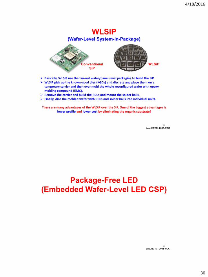
WLSiP (Wafer-Level System-in-Package)
Lau, ECTC- 2015-PDC 58
4/18/2016
30
Basically, WLSiP use the fan-out wafer/panel-level packaging to build the SiP. WLSiP pick up the known-good dies (KGDs) and discrete and place them on a
temporary carrier and then over mold the whole reconfigured wafer with epoxy molding compound (EMC).
Remove the carrier and build the RDLs and mount the solder balls. Finally, dice the molded wafer with RDLs and solder balls into individual units.
There are many advantages of the WLSiP over the SiP. One of the biggest advantages is
lower profile and lower cost by eliminating the organic substrate!
WLSiP (Wafer-Level System-in-Package)
Conventional SiP
WLSiP
Lau, ECTC- 2015-PDC 59
Package-Free LED (Embedded Wafer-Level LED CSP)
Lau, ECTC- 2015-PDC 60

4/18/2016
31
Package-Free LED (Embedded LED CSP)
Lau, ECTC- 2015-PDC 61
SUMMARY AND RECOMMENDATIONS
Out of the three methods in forming the FOWLP, chip-first with die-down is the most simple and low cost while chip-last (RDL-first) is the most complex and high cost. Chip-first with die-up requires slightly more process steps (and thus is slightly costly) than chip-first with die-down.
Chip-first FOWLP can perform more than what fan-in wafer-level packaging (WLP) can do. However, some of the things that PBGA (plastic ball grid array) package can do, but chip-first FOWLP cannot are: (1) larger die size (≥12mm x 12mm) and (2) larger package size (≥25mm x 25mm). This is due to the thermal expansion mismatch and warpage limitations of the chip-first FOWLP. In this case, chip-last (RDL-first) FOWLP can extend the application boundary to die size with the range of ≤15mm x 15mm and fan-out package size (≤32mm x 32mm). With the heat spreader wafer option, the boundary can even be stretched to die size of <20mm x 20mm and fan-out package size of <42mm x 42mm.
Chip-first FOWLP is just right for packaging semiconductor ICs such as baseband, RF/analog, PMIC, AP, low-end ASIC, CPUs (central processing units) and GPUs (graphics processing units) for portable, mobile, and wearable products. While chip-last (RDL-first) FOWLP is suitable for packaging the very high density and performance IC devices such as high-end CPUs, GPUs, ASIC, and FPGA (field programmable grid array) for high-end servers, computer, networking, and telecommunication products.
Lau, et al., CSR 20(3), 2016 62

4/18/2016
32
SUMMARY AND RECOMMENDATIONS
Out of the three methods for fabricating the RDLs, PCB technology with LDI is the cheapest, while Cu damascene is the most expensive. The method used will depend on the Cu line width/spacing and thickness of the RDLs. Usually, if the line width/spacing and thickness are <5µm and ≤2µm respectively, then Cu damascene is the preferred option; if they are ≥5µm and ≥3µm, then use polymer with ECD; and for >10µm and ≥5µm, PCB with LDI should be used.
For chip-first FOWLP, the choice of reconfigured wafer or panel depends on the Cu line width/spacing of RDLs. If it is >10µm, then use large (610mm x 457mm) panel, and combine with PCB/LDI and SMT P&P to increase throughput and to save cost.
For chip-first FOWLP, the curing temperature of polymers for RDL’s dielectric layer should be less than the critical temperature (230oC) of the compression molded EMC.
For chip-first FOWLP, the curing temperature of the EMC must be lower than the release temperature of the 2-side tape. For chip-first and chip-last FOWLP, high filler content EMC will shorten the time in mold, lower the mold shrinkage, and reduce the mold warpage. Uniform filler distribution and filler size of the EMC will reduce flow marks/fill and enhance flowability.
WLSiP is a cost-effective way to build low-profile and low-cost SiPs.
Embedded Wafer-level packaging is a low-cost and high throughput solution for package-free LED CSPs. Lau, et al., CSR 20(3), 2016
63
3D IC Integration
64

4/18/2016
33
CONTENTS Memory chip stacking
Wide I/O DRAM, Wide I/O2, or Hybrid
Memory Cube (HMC)
High Bandwidth Memory (HBM)
3D MEMS/IC Integration
65
3D IC Integration (The right thing to do!) Said the 1965 Nobel Physics laureate, Richard Feynman at the Gakushuin University (Tokyo) in 1985: “Another direction of improvement (of computing power) is to make physical machines three dimensional instead of all on a surface of a chip (2D). That can be done in stages instead of all at once – you can have several layers and then add many more layers as time goes on.” Thin
Chip
Micro Bumps
TSV
TSVs straight through the same memory chips to: enlarge the memory capacity lower the power consumption increase the bandwidth lower the latency (enhance electrical performance) reduce the form factor
will be the major applications of 3D IC Integration! Lau, ECTC-2008-PDC
66
4/18/2016
34
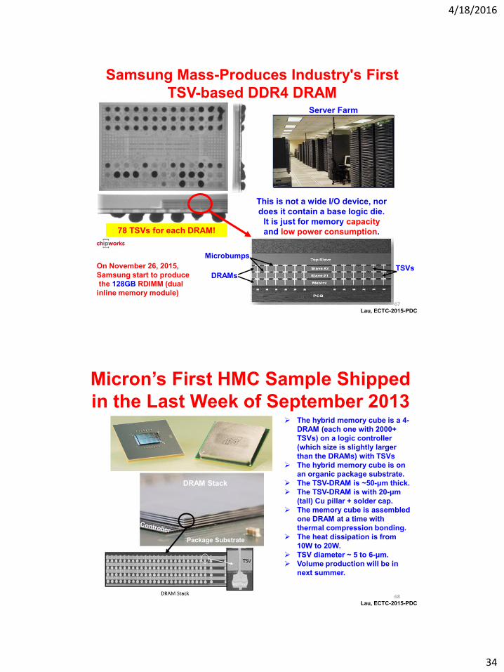
TSVs Microbumps
DRAMs
Samsung Mass-Produces Industry's First TSV-based DDR4 DRAM
This is not a wide I/O device, nor does it contain a base logic die.
It is just for memory capacity and low power consumption.
On November 26, 2015, Samsung start to produce the 128GB RDIMM (dual inline memory module)
78 TSVs for each DRAM!
Server Farm
Lau, ECTC-2015-PDC 67
Micron’s First HMC Sample Shipped in the Last Week of September 2013
The hybrid memory cube is a 4-DRAM (each one with 2000+ TSVs) on a logic controller (which size is slightly larger than the DRAMs) with TSVs
The hybrid memory cube is on an organic package substrate.
The TSV-DRAM is ~50-μm thick. The TSV-DRAM is with 20-μm
(tall) Cu pillar + solder cap. The memory cube is assembled
one DRAM at a time with thermal compression bonding.
The heat dissipation is from 10W to 20W.
TSV diameter ~ 5 to 6-μm. Volume production will be in
next summer.
DRAM Stack
Package Substrate
Lau, ECTC-2015-PDC 68
4/18/2016
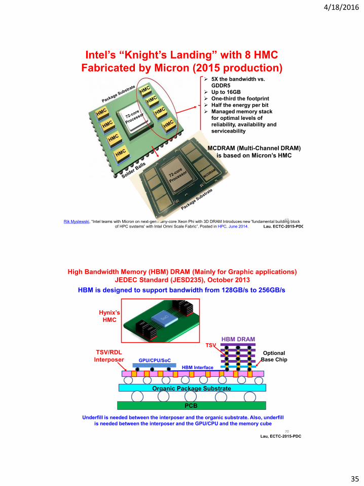
35
5X the bandwidth vs. GDDR5
Up to 16GB One-third the footprint Half the energy per bit Managed memory stack
for optimal levels of reliability, availability and serviceability
Intel’s “Knight’s Landing” with 8 HMC Fabricated by Micron (2015 production)
Rik Myslewski, “Intel teams with Micron on next-gen many-core Xeon Phi with 3D DRAM Introduces new 'fundamental building block of HPC systems' with Intel Omni Scale Fabric”, Posted in HPC, June 2014.
MCDRAM (Multi-Channel DRAM) is based on Micron’s HMC
Lau, ECTC-2015-PDC 69
Underfill is needed between the interposer and the organic substrate. Also, underfill is needed between the interposer and the GPU/CPU and the memory cube
GPU/CPU/SoC
Organic Package Substrate
PCB PCB
TSV/RDL Interposer
HBM Interface
HBM DRAM
Optional Base Chip
TSV
Hynix’s HMC
High Bandwidth Memory (HBM) DRAM (Mainly for Graphic applications) JEDEC Standard (JESD235), October 2013
HBM is designed to support bandwidth from 128GB/s to 256GB/s
Lau, ECTC-2015-PDC 70

4/18/2016
36
PTH
C4
GPU
HBM HBM
HBM HBM
TSV-Interposer
Build-up organic substrate
TSV
C4
GPU with microbumps Cu Solder
Microbump
4-2-4 Build-up substrate
Cu
Cu
TSV-Interposer
TSV-Interposer
1st DRAM
4th DRAM 3rd DRAM 2nd DRAM
AMD’s graph card made by Hynix’s HBM, which is TCB of the NCF DRAM chips one by one
71
Cu-pillar with solder cap
covered with NCF NCF Blade
Removing based film and dicing the bumped wafer with NCF
Chip
Substrate
Chip
Cu
Cu Solder
Chip
Chip
Chip
Substrate TCB with NCF (one chip at a time)
Heat and Pressure
Cutting to wafer size and backgringing
Base Film NCF
NCF Lamination for wafer Wafer
Chip Cu-pillar with solder cap Chip
Cu Solder cap
Wafer Bumping with Nonconductive Film (NCF) and FC bonding with NCF
Lau, et al., CSR, 19(5), 2015 72

4/18/2016
37
Conventional Stepwise Process of Stacked Chips by
Thermocompression Bonding (TCB)
It takes about 10 sec to cure the NCF and at the same time melt a solder and connect to an electrode on the substrate.
Toray, Sept. 2015, IEEE/3DIC conference 73
Peripheral portion Area portion
Stage temperature = 80oC
: Bond-force = 30N; Temp. = 150oC
1st step (3s): Bond-force = 50N Temp. = 220-260oC 2nd step (7s): Bond-force = 70N Temp. = 280oC
Toray’s Collective TCB of Stacked Chips
Toray, Sept. 2015, IEEE/3DIC conference 74

4/18/2016
38
SUMMARY TSVs straight through the same DRAMs is the right way to:
enlarge the memory capacity lower the power consumption increase the bandwidth lower the latency (enhance electrical performance) reduce the form factor
Unfortunately, due to the high-cost in making the TSVs and stacking the DRAMs, currently, it is used only for high-end servers, graphics and computers.
75
2.5D IC Integration and
TSV-Less Interposers
76

4/18/2016
39
CONTENTS
TSMC/Xilinx’s CoWoS
Xilinx/SPIL’s TSV-less SLIT
Amkor’s TSV-less SLIM
Intel’s TSV-less EMIB
ITRI’s TSV-less TSH
Shinko’s TSV-less i-THOP
77
Xilinx/SPIL’s TSV-less SLIT (Silicon-Less Interconnect Technology)
78

4/18/2016
40
4RDLs
TSV
Interposer
Cu Pillar
Solder
Si Chip
Devices (Cannot see)
Metal Layers
Metal Contacts
Micro Bump
C4
Xilinx/TSMC’s CoWoS
C4
C4
Si Chip
Cu Pillar Solder
4RDLs
Xilinx/SPIL’s SLIT
Package Substrate
Solder Ball
TSV and most interposer are eliminated! Only
RDLs remained.
Lower cost Better performance Lower profile
No entire TSV fabrication module
No thin wafer handling technology
No novel backside TSV revealing process
No multiple inspection & metrology steps for TSV fabrication & backside TSV revealing steps.
Micro-bump
65nm RDLs
C4/Contact via
Xilinx/SPIL IMAPS Oct 2014 79
(a) RDLs build-up on a Si-wafer
(b) Chip to wafer bonding (d) Over molding the whole wafer
(c) Underfilling
Si-wafer
Si-wafer Si-wafer
Si-wafer
RDL
Pad
CHIP CHIP
CHIP
Molding Compound
Passivation
Cu-Pillar Solder Solder
TSV-Less Interconnect Technology
80

4/18/2016
41
CHIP Molding Compound
Passivation (e) Reinforced wafer and Backgrind the Si-wafer
CHIP
(g) Cu plating
CHIP CHIP
Passivation
(f) Passivation, photoresist, mask, litho, etch passivation, sputter Ti/Cu, photoresist, mask, litho. (h) Strip photoresist, etch Ti/Cu, C4 bumping
C4
Reinforcement Wafer (Heat Spreader)
Cu Contact pad Ti/Cu UBM
Reinforcement (Heat Spreader)
Molding Compound
Underfill Cu-Pillar Solder Pad
RDL RDL
TSV-Less Interconnect Technology
81
CHIP
Passivation
C4
Package Substrate
PCB
Underfill
Molding Compound
Cu-Pillar Solder Solder
Solder Ball
TSV-Less Interconnect Technology Reinforcement (Heat Spreader)
Contact pad UBM
RDL RDL
Pad
82

4/18/2016
42
Amkor’s TSV-less SLIM (Silicon-Less Integrated Module)
83
Foundry BEOL layers retained Same CuP bond pads Same UBM and solder bump No TSV Much thinner
Amkor’s SLIM (Silicon-Less Integrated Module)
Interposer
TSV
RDLs
Amkor, 11th International Conference and Exhibition on Device Packaging, 2015.
4/18/2016
43
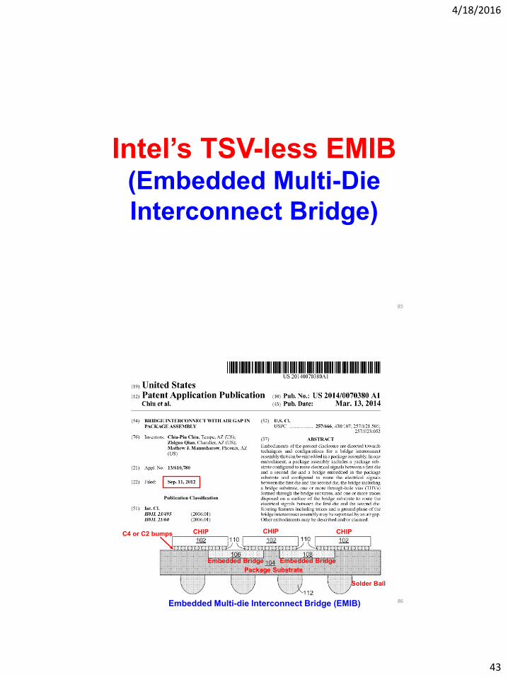
Intel’s TSV-less EMIB (Embedded Multi-Die Interconnect Bridge)
85
CHIP CHIP CHIP C4 or C2 bumps
Package Substrate
Solder Ball
Embedded Bridge Embedded Bridge
Embedded Multi-die Interconnect Bridge (EMIB) 86

4/18/2016
44
PCB Solder Ball
Package Substrate EMIB EMIB
FPGA HBM HBM
Microbump/C4 bumps
Heterogeneous Integration using Intel’s EMIB and Altera’s FPGA Technology
RDL RDL
87 Intel/Altera, November 2015
Package Substrate
Solder Ball
C4 or C2 Bumps
Embedded Bridge
Bare Si-wafer with RDLs and Contact Pads
Contact Pad
RDLs SiO2
Cross-section view Top view
CHIP B CHIP A
Intel’s Embedded Multi-die Interconnect Bridge (EMIB)
Embedded Multi-die Interconnect Bridge (EMIB) 88
4/18/2016
45
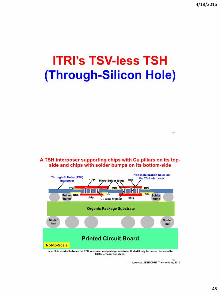
ITRI’s TSV-less TSH (Through-Silicon Hole)
89
Organic Package Substrate
Solder bump
RDL RDL RDL
RDL RDL
Cu wire or pillar
Micro Solder joints
RDL
chip Through-Si Holes (TSH)
Interposer
Non-metallization holes on the TSH interposer
chip chip
chip
Solder bump
Solder ball
Solder ball
Printed Circuit Board Not-to-Scale Underfill is needed between the TSH interposer and package substrate. Underfill may be needed between the
TSH interposer and chips.
A TSH interposer supporting chips with Cu pillars on its top-side and chips with solder bumps on its bottom-side
Lau et al., IEEE/CPMT Transactions, 2014 90

4/18/2016
46
PCB
Top Chip
TSH Interposer
Package Substrate
Underfill Cu-Pillars
Holes in the TSH Interposer
Solder bumps between TSH
Interposer and package substrate
Solder bumps between TSH
Interposer and Top- Chip and Bottom-Chip
(a) (b)
Top Chip Cu Pillar
PCB
Bottom Chip
Non-metallization holes on the TSH interposer
Package Substrate
TSV-Less Interposer – TSH Interposer
Lau et al., IEEE/CPMT Transactions, 2014 91
Shinko’s TSV-less i-THOP (Integrated Thin film High density Organic Package)
92

4/18/2016
47
Chip Chip
Chip-to-chip interconnection through 2µm width traces
Thin Film (2 layers + FC Pad)
Conventional Build-up
Substrate (1-2-2)
40µm-pitch Pads
Chip1
Chip2
2µm line width/spacing (C2C connection)
Chip1 Chip2
Chip1 Chip2
Shinko’s 2.5D IC Integration without TSVs
Shinko, ECTC 2014 93
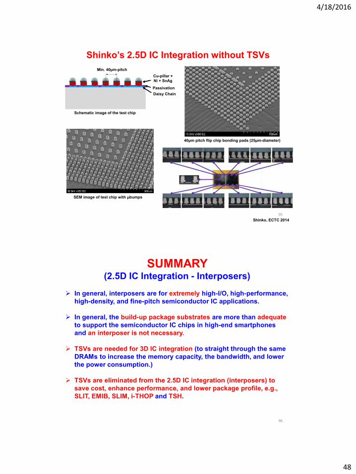
Passivation
Min. 40µm-pitch Cu-pillar + Ni + SnAg
Daisy Chain
Cu-OSP (Organic Solderability Preservation)
ENEPIG (Electro-less Ni/Pd/Au plating)
SEM image of test chip
Schematic image of the test chip
40μm pitch flip chip bonding pads (25µm-diameter)
Shinko’s 2.5D IC Integration without TSVs
Shinko, ECTC 2014 94
4/18/2016
48
SEM image of test chip with µbumps
Passivation
Min. 40µm-pitch Cu-pillar + Ni + SnAg
Daisy Chain
Schematic image of the test chip
40μm pitch flip chip bonding pads (25µm-diameter)
Shinko’s 2.5D IC Integration without TSVs
Shinko, ECTC 2014 95
SUMMARY (2.5D IC Integration - Interposers)
In general, interposers are for extremely high-I/O, high-performance,
high-density, and fine-pitch semiconductor IC applications.
In general, the build-up package substrates are more than adequate to support the semiconductor IC chips in high-end smartphones and an interposer is not necessary.
TSVs are needed for 3D IC integration (to straight through the same DRAMs to increase the memory capacity, the bandwidth, and lower the power consumption.)
TSVs are eliminated from the 2.5D IC integration (interposers) to save cost, enhance performance, and lower package profile, e.g., SLIT, EMIB, SLIM, i-THOP and TSH.
96

4/18/2016
49
Thank you very much for your attention!
97