Embed Size (px)
Citation preview

ICECS, Athens , December 2010 1/18
From nanoscale technology scenarios to compact device models for
ambipolar devices
Sébastien Frégonèse, Cristell Maneux, Thomas Zimmer
CNRS,
Université Bordeaux,
UMR 5218, Laboratoire IMS, Bordeaux

2/18ICECS, Athènes , December 2010
• Introduction
• Development of a dual-gate compact model– Material parameter
– Drain current modeling
– Charge modeling
– Equivalent circuit and self-consistent potential calculation
• Comparison of compact model with measurement of the literature
• Circuit simulation
• Conclusion
Outline

3/18ICECS, Athènes , December 2010
• New materials: – Nanowire
– Carbon nanotube (single wall : 1993)
– Graphene and graphene nanoribbon (2004)
(Nobel Prize 2010)
Introduction
New transistors
4/18ICECS, Athènes , December 2010
Introduction
Y.-M. Lin, J. Appenzeller, J. Knoch, and Ph. Avouris, “High performance carbon nanotube field-effect
transistor with tunable polarities,” IEEE Trans. On Nanotech., vol. 4, N° 5, pp. 481–489, September 2005
New transistor development using emerging material
Open new design paradigm

5/18ICECS, Athènes , December 2010
I. O’Connor, J. Liu, F. Gaffiot, F. Prégaldiny, C. Lallement, C. Maneux, J. Goguet, S. Frégonèse, T. Zimmer, L. Anghel, TT Dang, R. Leveugle, “CNTFET Modeling and Reconfigurable
Logic-Circuit Design”, IEEE Trans. On Circuits And Systems I, Vol. 54, No. 11, November 2007 pp 2365-2379
IntroductionPossibility to develop new reconfigurable logic cells
Needs an accurate compact model to :
- validate the approach
- evaluate the performances
-develop new structures

6/18ICECS, Athènes , December 2010
Tunneling (SB)
Inner partSource access
Drain access
D
Si (P++)
SiO2
S DCNT
DG-CNTFET
Al
Al2 O3
Introduction
Vdi
Vsi
source
drain
Sn
DnVCNTS
VCNTD
VCNTi
Thermionic transport
Electrostatic control with back-gate
Electrostatic control with front-gate
Schottky barrier
Carrier Charge
Valence Band
Conduction Band
FG D
BG
Ti

7/18ICECS, Athènes , December 2010
J. C. Charlier et al. , Rev. Mod. Phys., Vol. 79, No. 2, April–June 2007
Density of statesBand structure
Zone Folding model of a (10,0) nanotubeNumerical calculation
Analytical model for Density of states• subband value• effective mass• non-parabolicity parameter
Material parameter
Input data for charge model and drain current model
8/18ICECS, Athènes , December 2010
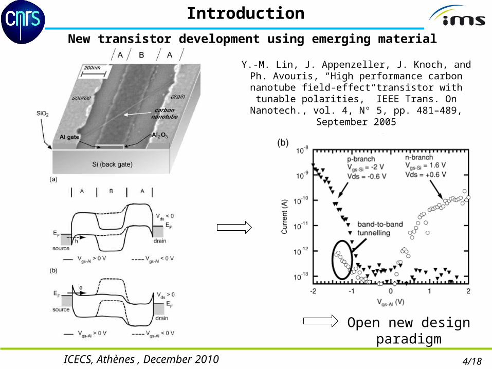
DEF
DEF
q(VSi-VCNT)-sbbd[1]
qVSi
qVDi
Current spectrum in a MOS-like CNTFET using NEGF simulation *
VCNTi
IDS
60mV/decOhmic behavior
Slope > 60mV/decSchottky behavior
Source exhaustion
BTBT behavior
0 0
2S S D D
eI M f E T E dE f E T E dE
h
Thermionic contribution
BTBT
• Thermionic contribution : T(E) = 1 above conduction band = 0 otherwise
• BTBT contribution : T(E) = for E =[CB access, VB channel]
0 otherwise
, ,
, , , ,
BTBT S BTBT D
BTBT S BTBT D BTBT S BTBT D
T T
T T T T
* NEGF simulator is originally created in Purdue University
Drain current modeling

9/18ICECS, Athènes , December 2010
Charge modeling
MAX ,
MAX ,
_MAX , ,
MAX ,
MAX , ,
MAX ,
2
2
2
2
Sn I
I Dn
Sn I Dn
I Dn
Sn I D
I Sn
SCB
DCB
IP eCB
DCB
CB CB
SCB
D Ef E dE
D Ef E dE
Q eD E
f E dE
D Ef E dE
Analytical approximate solution proposed in IEEE Trans Elec. Devices
Vdi
Vsi
source
drain
Sn
Dn
Dp
Sp
integration limits for carrier coming from source
integration from Sn to
integration limits for carrier coming from drain
:CBi inner
conduction band
integration from CBi to
integration from SnCBi to
Carriers from the drain are reflected on the source SB
valence band
VCNTSVCNTD
VCNTi
Same method is applied for electrons and holes and in each region

10/18ICECS, Athènes , December 2010
CNTi
Si
Di
VD
VS
FG FGx FGi
,IP DdQ
dt
,IP SdQ
dt
VFB-FG CFGRG
RS
RD
CDEi
CSEi
IDS IBTBT
CNTd
CNTs
FGi BG
BGix
,SA DdQ
dt
,DA DdQ
dt
,SA SdQ
dt
,DA SdQ
dt
CBGS
BGiD
BGiS
CBGD
RBGD
RBGS
VFB-BG
CNTs
CNTd CDEx
CSEx
CG_coup. /2
CG_coup. /2
CNTi
0.5*CBGi
CNTi
0.5*CBGi
Optional elementsCore of the model
Equivalent circuit
, , ,,
, , ,,
, , ,,
SEi CNTi S SEx Si S BGiS S BGS S SCNTs S
BGS S SEi SEx
DEi CNTd S SEi CNTs S Gi S FG I iCNTi S
FG I SEi DEi
DEi CNTi S DEx Di S BGiD S BGD D DCNTd S
BGD D DEi DEx
C V C V V C L QV
C L C C
C V C V V C L QV
C L C C
C V C V V C L QV
C L C C
Self consistent potential
calculation in each region
Thermionic, SB, BTBT current
Charge in inner part from Source
Charge in inner part from Drain
Charge in Source and Drain access
from Drain
Charge in Source and Drain access
from Source

11/18ICECS, Athènes , December 2010
Validation of the model: comparison with the IBM device
1.E-14
1.E-13
1.E-12
1.E-11
1.E-10
1.E-09
1.E-08
1.E-07
1.E-06
-1.50 -1.00 -0.50 0.00
I DS
[A]
VFGS [V]
measurement
simulation
VDS
Y.-M. Lin, J. Appenzeller, J. Knoch, and Ph. Avouris, vol. 4, N° 5, pp. 481–489, September 2005
1.E-14
1.E-13
1.E-12
1.E-11
1.E-10
1.E-09
1.E-08
1.E-07
1.E-06
-1.50 -1.00 -0.50 0.00
I DS
[A]
VFGS [V]
measurement
simulation
VBGS
1.E-14
1.E-13
1.E-12
1.E-11
1.E-10
1.E-09
1.E-08
1.E-07
1.E-06
-2.00 -1.50 -1.00 -0.50 0.00I D
S[A
]
VFGS [V] (VFGS=VBGS)
measurement
simulation

12/18ICECS, Athènes , December 2010
0
2
4
6
8
10
12
14
0.00 0.50 1.00
-I DS
[µA]
-VDS [V]
measurement
Simulation
Validation of the model: comparison with the Stanford device
1.E-12
1.E-11
1.E-10
1.E-09
1.E-08
1.E-07
1.E-06
-1.00 0.00 1.00 2.00
I DS
[A]
VBGS [V]
measurement
simulation
VDS=10mV
1.E-11
1.E-10
1.E-09
1.E-08
1.E-07
1.E-06
1.E-05
1.E-04
-2.00 -1.50 -1.00 -0.50 0.00
I DS
[A]
VFGS [V]
measurement, VBG=-2 V
simulation, VBG=-2V
measurement, VBG=-2.5V
simulation, VBG= -2.5V
VBG=-2.5V VDS=300mV
VDS, VBG=-2V
A. Javey, et al., Nano Letters, vol. 4, Mar.
2004, p. 447-450
Prior front gate fabrication

13/18ICECS, Athènes , December 2010
D
S
FG BG
Evaluation of parasitic element with TCAD
Parasitic parameter extractionto metal 1
Finite element
simulation

14/18ICECS, Athènes , December 2010
+VBG
-VBG
+VBG
-VBG
+VBG
-VBG
+VDD
Circuit application: voltage controlled ring oscillator
Parameters used in the simulation are the one obtained from the IBM
technology except VFB which is reduced to have a better symmetry of the CMOS
like inverter
5 stages ring oscillatortime [s] [E-6]
Vou
t [V
], V
bg=+/-3V
V
out [V
], V
bg=+/-2.
5V V
out [V
], V
bg=+/-2.
25V
[E
-3]
8 10 12 14 16 18 20-200
0
200
400
600
800
[µS]
[mV]

ICECS, Athènes , December 2010 15/18
• A compact model dedicated to dual gate device – Drain current modeling
– Charge modeling
– Equivalent circuit
• Validation with measurement from 2 different technologies– Stanford University
– IBM
• Circuit simulation– Parasitic element
– Voltage controlled oscillator
• Outlook– Main limitation for technology developpement: control of nanotube chirality
and density• Technological breakthrough needed
Conclusion

16/18ICECS, Athènes , December 2010
Outlooks
“Dual-gate Graphene FETs With fT of 50 GHz”, LIN et al., IEEE EDL, VOL. 31, NO. 1, JANUARY 2010
“Dual-gate silicon nanowire transistors with nickel silicide contacts”J. Appenzeller et al.1IBM, 2Institute for Thin Film and Interfaces,Julich
Alternative solutions for dual gate devices
Model can be easily extended to graphene nanoribbon and very small nanowire (1D and ballistic)
17/18ICECS, Athènes , December 2010
• Work was supported by the French National Research Agency ANR through ARPEGE “NANOGRAIN” project.
• The authors would also like to thank all partners of this project for the fruitful discussions.
Acknowledgement
ICECS, Athènes , December 2010 18/18
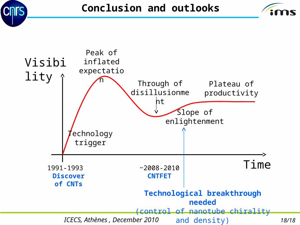
Conclusion and outlooks
Time
Visibility
Technology trigger
Peak of inflated
expectation
Through of disillusionment
Plateau of productivity
Slope of enlightenment
1991-1993Discover of
CNTs
~2008-2010CNTFET
Technological breakthrough needed(control of nanotube chirality and density)
19/18ICECS, Athènes , December 2010
J ds / per tube [LOG] fT
with
12
tube
s / 50
nm fT
with
6 tub
es / 5
0nm
fT
with
1 tub
e / 50
nm [E
+9]
1E-8 1E-7 1E-6 1E-50
200
400
600
800
Performance of an optimized structure
20nm
50nm
50nm
• SB height is optimized to get ambipolar symmetric behavior
• Optimize ION current for both N an P behavior
• Back-gate insulator is optimized to improve the tradeoff between parasitic and SB thickness control (ION current)
1 tube /50 nm
12 tubes /50 nm(Optimum theoretical limit with this configuration)
6 tubes /50 nm

20/18ICECS, Athènes , December 2010
Calculation of the Schottky barrier
Z. Chen, J. Appenzeller, J. Knoch, Y. Lin, and P. Avouris, “The Role of Metal-Nanotube Contact in
the Performance of Carbon Nanotube Field-Effect Transistors”, Nano Letters, 2005, Vol. 5,
No. 7, 1497-1502
0.123meV on Valence band
side
21/18ICECS, Athènes , December 2010
Modeling: Tunneling through Schottky barrier
_ / 1 / , exp / 1 / ,SBeff S D SB tunnelsbbd V cnts cntd si d sbbd V cnts cntd si
Fitting parameter
Effective Schottky barrier model
WKB calculation
• Tunneling through barrier is usually performed using WKB approximation
• WKB is too complex to obtain analytical expression of current
=> Effective Schottky barrier approach*
*Knoch, J.; Appenzeller, J., physica status solidi (a), vol. 205, issue 4, pp. 679-694
(2008).
22/18ICECS, Athènes , December 2010
_max , 1 ,Sn SBeff S sbbd V cnts si
Thermionic / Schottky Current modeling
_
1
max , [ ] ( , ),ln 1 exp
4
max , [ ] ( , ), ( , )ln 1 exp
Sn Dn
nb sbbdBB
DS ep Sn Dn
B
sbbd p V cnti s
k Tek TI
h sbbd p V cnti s V di si
k T
Transition between Thermionic /Schottky behavior:
Vdi
Vsi
source
drain
Sn
Dn
DpSp
:CBi conduction band
Thermionic contribution
SB tunnel contribution
:VBi valence banda)
VCNTi
Log IDS
60mV/decMos-like behavior
Slope > 60mV/decSchottky behavior
Source exhaustion
b)
Landauer equation
Electron contribution:

23/18ICECS, Athènes , December 2010
MAX ,
_
MAX ,
2I
Sn Dn
I
Sn Dn
VB
Sn
BTBT e BTBT VB
Dn
f E dEMq
I Th f E dE
, ,
, , , ,
BTBT S BTBT DBTBT
BTBT S BTBT D BTBT S BTBT D
T TT
T T T T
* 3/ 2
,
4 2 (2 [ ])exp
3
S D
BTBT S DS D
m sbbd pT
q V
D
VCNTi
IDS
60mV/decOhmic behavior
Slope > 60mV/decSchottky behavior
Source exhaustion
BTBT behavior
BTBT Current modeling
Analytical model:
Analytical solution is straightforward
DEF
DEF
q(VSi-VCNT)-sbbd[1]
qVSi
qVDi
Current spectrum in a MOS-like CNTFET using NEGF simulation *
* NEGF simulator is originally created in Purdue University