Embed Size (px)
Citation preview

IC manufacturing test cost estimation at early stages of the design cycle
Tom Chena,* , Von-Kyoung Kim a, Mick Tegethoffb,1
aDepartment of Electrical Engineering, Colorado State University, Fort Collins, CO 80523, USAbManufacturing Test Division, Hewlett-Packard Company, Loveland, CO, USA
Accepted 20 November 1998
Abstract
This article presents a test cost prediction model as a planning tool at an early stage of the design cycle to estimate manufacturing test costof ICs. The proposed cost model estimates the IC manufacturing test cost based on test throughput. The model calculates test throughput byincorporating IC yield and fault coverage. Chip manufacturing information was used to predict the test cost and test quality in ICmanufacturing test. The objective of the cost model is to better plan IC product design and reduce cost by predicting the IC manufacturingtest cost at an early stage of the design cycle without relying on detailed information such as layout or even netlist. The proposed model wasapplied to a commercial ASIC product. The model estimation result showed an acceptable accuracy as a first order approximation tool.q 1999 Elsevier Science Ltd. All rights reserved.
Keywords:Manufacturing test cost; Cost model; Cost prediction; Test time
1. Introduction
VLSI technology has undergone a rapid growth of inte-gration density. The increasing complexity and the decreas-ing geometries make it common to integrate millions ofcomponents on a single silicon die. However, the ever-increasing scale of integration causes many difficultproblems in the testing of highly integrated ASICs. Increas-ing chip’s complexity without employing correct DFT tech-niques usually results in a significant degradation in productquality later on in the manufacturing phase or costly rede-sign. A correct design methodology based on a correct testcost prediction nearly on in the design cycle can shorten thedesign cycle, stay within the budget, and meet the evertightening time-to-market requirement. To achieve thisgoal, a method to estimate manufacturing test cost earlyon in the design cycle is essential. The test cost predictionmodel must not rely on detailed circuit information such aslayout or even netliet.
The idea of modelling the cost of manufacturing test hasbeen explored by others in the past. Dislis et al. [1,2] andDear et al. [3] proposed a test strategy selection tool, which
helps to find the optimum test strategy for a given set ofcircuit characteristics. Although their tools can select theoptimum test strategy based on the characteristics of agiven circuit, finding the absolute metrics for the cost andquality of a manufacturing test remains to be a challengingproblem. Abadir et al. [4] developed Hi-TEA, a multi-chipmodule (MCM) testing strategy selection tool, which helpsto select the cost-effective test strategy for MCMs. Theirtool requires cost parameters such as die test cost andwafer yield, which are difficult to obtain in the early stageof a design cycle. Therefore, their tool may not be practicalto predict a chip test cost early on. Druckerman et al. [5]investigated the cost trade-offs of popular DFT techniques.Their results can also be used for selecting the DFT strategy,however their method does not provide an early testing costestimation. Dick et al. [6] did sensitivity analysis overdifferent test cost parameters. Their result showed that fivecircuit parameters dominate prediction accuracy while themodel was relatively insensitive to the other cost para-meters. The five important parameters are the productionunit cost, the sequential depth, the production volume, thegate count, and the required fault coverage. Unfortunately,some of these parameters, such as the sequential depth, aredifficult to obtain in the early stage of the design processwhere the circuit netlist may not even be available.
We propose a new IC test cost model which can be usedas a planning tool for predicting IC manufacturing test costearly in the design cycle. The model takes basic test cost
Microelectronics Journal 30 (1999) 733–738
MicroelectronicsJournal
MEJ 546
0026-2692/99/$ - see front matterq 1999 Elsevier Science Ltd. All rights reserved.PII: S0026-2692(98)00159-1
* Corresponding author. Tel.:11-970-491-6574; fax:11-970-491-2249.
E-mail addresses:[email protected] (T. Chen), [email protected] (M. Tegethoff)
1 Tel.: 11-970-679-5580

parameters from manufacturing environments. In order tofacilitate early predictions, the cost parameters were simpleenough so that they are easy to obtain in the early stage ofthe design process. The proposed prediction model also usesa set of design parameters such as the number of IOs andflip-flops of the circuit under test. With ever increasingamount of design reuse, these parameters can be easily esti-mated without having to generate detailed netlists orlayouts.
This article is organized as follows: Section 2 discussesthe basic elements of IC test economics and the proposed ICmanufacturing test cost model. Section 2.1 gives an over-view of the cost model, Section 2.2 and 2.3 describe the ICyield prediction and fault coverage prediction. A new testthroughput model is shown in Section 2.4. Section 3discusses an example of model application to a commercialproduct. Finally, Section 4 concludes the article.
2. Manufacturing test cost model
2.1. Overview
The proposed ASIC test cost model consists of two majorparts, test time prediction model and test cost rate (TCR)model. Fig.1 shows the inputs and outputs of the model,while Fig. 2 shows the organization of the model. The testtime model predicts an approximate chip testing time usingthe fault coverage estimation from a fault coverage model[7]. ASIC chip yields can be predicted using the sensitivearea estimation through sensitive area models [8,9]. A sensi-tive area is the area, which is sensitive to the processingdefects. The sensitive area affects IC manufacturing yield.It is also referred to as a critical area or an effective area inother studies. We use sensitive area and critical area inter-changeably in this article. The fault coverage modelemploys three different test strategies, which are randomtesting, IDDQ testing, and full scan testing. The estimatedfault coverage depends on the selected test strategy andother circuit parameters, such as the gate count and the IOcount. The TCR model is relatively simple compared to thetest time model, because the TCR is usually determined bythe test platform and it would not change significantlywithin the same platform. Once the test time and TCR areestimated, the test cost can be calculated.
2.2. Yield estimation
The chip yield is one of the most dominant factors todetermine the overall chip manufacturing cost. Chip’smanufacturing yield can be estimated using one of themany available yield prediction models [10–16]. A detaileddiscussion on IC yield models can be found in [17]. Each ofthe IC yield models has its own strengths as well as limita-tions. Selecting an incorrect yield model often causes a largeerror in IC yield prediction. Therefore, a correct yieldformula selection is important to make the prediction
T. Chen et al. / Microelectronics Journal 30 (1999) 733–738734
Fig. 1. Test time and TCR.
Fig. 2. Test cost estimation.

valid. Maly [18] and Gaitonde et al. [19] found that ASICyield prediction using a whole chip area is inaccurate andmisleading, and often yields too pessimistic predictions.The chip yield prediction using a whole chip area in alarge die often results in pessimistic yield projection,because the large chip area exaggerates the probability ofhaving fatal defects. Using a sensitive area model, a moreaccurate IC yield prediction is possible.
More and more VLSI ASICs are employing embeddedmemory cores. On a single chip, maximizing the perfor-mance by eliminating the data transfer bottlenecks betweenmemory and logic. Recognizing the different characteristicsbetween the logic and memory portions on the same chip,two different types of sensitive areas are estimated sepa-rately. The two sensitive area models for logic and memorywere discussed in the previous articles [8,9], and shown herein Eqs. (1) and (2). The sensitive area for the logic portion,SALOGIC, is a function of the gate count, the net count, andthe underlining technology; while the sensitive area for thememory portion, SAMEMORY, is a function of the memoryarray size and the underlining technology. The total sensi-tive area (TSA) is the summation of the two sensitive areas.The parameters of the proposed sensitive area predictionmodels are easy to obtain in the early stage of the designcycles. The sensitive area model for logic is
SALOGIC � c0 1 c1 × G2 1 c2 ×���Np
; �1�where,G is the gate count,N is the net count, andc0, c1, c2
are model coefficients. The sensitive area model for memoryis
SAMEMORY � �c3 1 c4 × P� × M; �2�where,P is the underlining process technology (minimum
feature size),M is the memory capacity, andc3, c4 are modelcoefficients. Finally, the TSA of the chip is
TSA� SALOGIC 1 SAMEMORY: �3�The yield of an ASIC chip yield can be estimated using
the fabrication defect density, DD, and the sensitive area,SA, of the ASIC chip. Consequently, the number of passeddies, NPD, and the number of failed dies, NFD, can beestimated with the projected chip yield,Y. Eqs. (4)–(6)show the relationship betweenY and NPD/NFD.
Y � e2DD×SA; �4�
NPD� NDW × NWL×Y; �5�
NFD� NDW × NWL × �1 2 Y�; �6�where, NDW and NWL are the number of dies per wafer,and the number of wafers per lot, respectively.
2.3. Fault coverage estimation
The fault coverage model used to estimate the overall testcost is shown in Eq. (7) and illustrated in Fig. 3. Fig. 3 showstwo different fault coverages of Chipn and Chipm. Let LBbe the fault coverage lower bound as the starting fault cover-age, and UB be the fault coverage upper bound as the satur-ating fault coverage. Also, definea and A as the rate ofincrease, and the difference between LB and UB. Forexample, fault coverage comparison of two ISCAS bench-mark circuits, C5315 and C6288, is given in Table 1. Bothcircuits have about the same UB value, but C6288 has ahigher a value than that of C5315. Therefore, the faultcoverage of C6288 would be saturated faster than C5315.The details of the fault coverage model can be found in [7].
C �F�test_length� � C0 2 A × e2a×test_length: �7�
Finding the optimum test pattern length, TLopt, iscritical in test economics. The first derivative of faultcoverage model, shown in Eq. (8), represents the rate ofchange in fault coverage with regard to the test length.Theoretically, TLopt can be found when dC/dtest_lengthis zero. However, practically, when fault coveragereaches a saturation point (i.e. T1 and T2 points inFig. 3), dC/dtest_length can be a very small valuebut not zero. Therefore, we set TLopt to be where dC/dtest_length becomes just below the user-setting thresh-old valueCth. Eq. (9) is obtained by solving Eq. (8) forTLopt. Further, the actual test used in manufacturing isoften longer than the theoretical TLopt value. Therefore,we added an adjustment factor,b , so that TLactual �b × TLopt.
dCdtest_length
� a × A × e2atest_length# Cth; �8�
TLopt � 21a
� �ln
Cth
aA
� �: �9�
T. Chen et al. / Microelectronics Journal 30 (1999) 733–738 735
Fig. 3. Chip fault coverage model.
Table 1Fault coverage comparison of C5315 and C7552
Circuit Gate IO UB LB a A
C5315 1145 301 0.9571 0.2772 0.1970 0.8280C6288 1848 64 0.9650 0.3889 0.2903 0.7702

Knowing the chip yield and fault coverage, one canpredict the chip defect level. Williams and Brown [20]proposed the well-known defect level formula which isshown in Eq. (10). The defect level reflects the overall testquality of a given chip.
DL �F�Y;C� � 1 2 Y12C: �10�
2.4. Testing time estimation
The intrinsic chip test time is the time required for testinga single chip. The use of intrinsic test time as a measure forchip testing cost in a manufacturing environment is oftenmisleading and inaccurate, because intrinsic test time doesnot consider test setup time (TST). In practice, test through-put is much more meaningful than the intrinsic testing time,because it reflects real manufacturing test situations byincorporating TST and extra time required for the manufac-turing test. The test throughput is defined as the averagenumber of chips processed by a testing platform during aunit time period. The test cost is proportional to the testingtime, while chip testing time is inversely proportional to thethroughput. Therefore, a higher throughput reduces testingcost in a manufacturing environment, ensures cost-effectiveproduction. The test throughput is affected by many para-meters. Among the parameters, the TST, the wafer loadingtime (WLT), the number of wafers per processing lot(NWL), the number of dies per wafer (NDW), the chipyield (Y), the chip testing time for a good die, TPASS, andthe average chip testing time to screen a bad chip, TFAIL arerecognized as the important parameters to estimate the testthroughput.
The main advantage of calculating the test throughput isthe capability of identifying the different testing environ-ments in the manufacturing. In practice, two different
testing situations may exist. The first situation is for testinglarge quantity, but small number of products, and the secondsituation is for testing small quantity, large number ofproducts. The typical products in the first situation mayinclude semiconductor memories and microprocessorchips, and the typical products in the second situation mayinclude ASIC products. In the first situation, the testthroughput is close to the intrinsic testing time. However,in the second situation, the test throughput significantlydiffers from the intrinsic testing time, because of the extraTST for different products. As a result, the selection of testplatform, the selection of products to be tested, and themanufacturing test strategy should be optimized in orderto maximize the test throughput.
where,g is the fraction of TFAIL to TPASS.
COST� TCHIP × TCR �13�The average testing time of a chip can be approximated
using a set of parameters. Table 2 summarizes the test envir-onment data used in our model for test time estimation. Eq.(11) gives the average testing time. The numerator of Eq.(11) is the total testing time for an wafer lot, and the denomi-nator is the total number of chips tested. TST is the TST toload test program and test patterns. WLT× NWL representstotal wafer loading time, where WLT is the wafer loadingtime and NWL is the number of wafers per lot. DST×NDW × NWL represents total die stepping time , whereDST is the unit die stepping time, NDW× NWL is thetotal number of dies per lot.TPASS × NPD is the total testtime for passing good dies, andTFAIL × NFD is the total testtime for screening bad dies. The total testing time for atesting lot can be estimated if TST, TLT,TPASS, TFAIL,NPD, and NFD are known. Among them, the intrinsic test-ing time of a good chip,TPASScan be estimated by the faultcoverage model using a given set of circuit parameters. NPDand NFD also can be estimated by the chip yieldY, which ispredicted by the sensitive area model. TST and WLT can beeasily obtained for a given test platform and test environ-ment.TPASS can be estimated by Eq. (9). If a set of severaldifferent tests were used,TPASS would be the summation oftest times for all tests. For example, a set of three tests,functional, scan, andIDDQ tests were applied for testing anIC. TPASSfor this IC is the summation of test time for func-tional, scan, andIDDQ tests. The average test time to screen abad chip,TFAIL is left as an unknown parameter, because itdepends on the test flow, type of the test, and manufacturingline characteristics. In practice, test engineers rearrange thetest flow to detect maximum number of defective parts inthe earliest stage of the test flow. Therefore, initialTFAIL
T. Chen et al. / Microelectronics Journal 30 (1999) 733–738736
Table 2Testing environment data
NWL Net wafer per lotNDW Net die per waferNPD Net passed dieNFD Net failed dieTST Test setup timeWLT Wafer loading timeDST Die stepping timeSTR Scan test rateMTR Memory test rateITR Iddq test rateFDD Fab defect densityMTA Memory test algorithmTCR Test cost rate
TCHIP � TST1 WLT × NWL 1 DST× NDW × NWL 1 TPASS× NPD1 TFAIL × NFDNDW × NWL
� TST1 WLT × NWL 1 DST× NDW × NWL 1 TPASS× NPD1 NFD=gÿ �
NDW × NWL�11�
value may be significantly larger than the final, optimizedTFAIL value. Hirase [21] approximated TFAIL to a quarter ofTPASS. In our model,g is the ratio of the testing time for abad die to the testing time for a good die. Finally, the aver-age chip testing cost in a manufacturing environment can beestimated byTCHIP and TCR. Eqs. (11) summarize theproposed IC manufacturing test cost model.
3. Application of the model
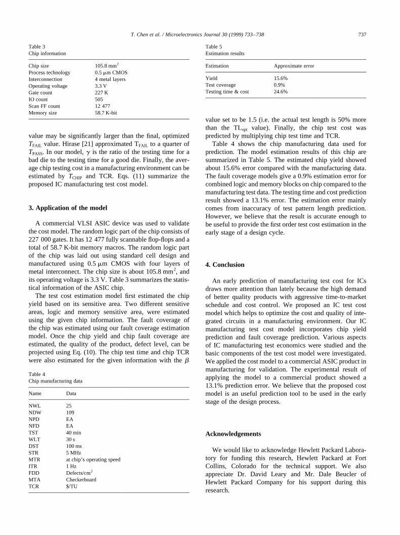
A commercial VLSI ASIC device was used to validatethe cost model. The random logic part of the chip consists of227 000 gates. It has 12 477 fully scannable flop-flops and atotal of 58.7 K-bit memory macros. The random logic partof the chip was laid out using standard cell design andmanufactured using 0.5mm CMOS with four layers ofmetal interconnect. The chip size is about 105.8 mm2, andits operating voltage is 3.3 V. Table 3 summarizes the statis-tical information of the ASIC chip.
The test cost estimation model first estimated the chipyield based on its sensitive area. Two different sensitiveareas, logic and memory sensitive area, were estimatedusing the given chip information. The fault coverage ofthe chip was estimated using our fault coverage estimationmodel. Once the chip yield and chip fault coverage areestimated, the quality of the product, defect level, can beprojected using Eq. (10). The chip test time and chip TCRwere also estimated for the given information with theb
value set to be 1.5 (i.e. the actual test length is 50% morethan the TLopt value). Finally, the chip test cost waspredicted by multiplying chip test time and TCR.
Table 4 shows the chip manufacturing data used forprediction. The model estimation results of this chip aresummarized in Table 5. The estimated chip yield showedabout 15.6% error compared with the manufacturing data.The fault coverage models give a 0.9% estimation error forcombined logic and memory blocks on chip compared to themanufacturing test data. The testing time and cost predictionresult showed a 13.1% error. The estimation error mainlycomes from inaccuracy of test pattern length prediction.However, we believe that the result is accurate enough tobe useful to provide the first order test cost estimation in theearly stage of a design cycle.
4. Conclusion
An early prediction of manufacturing test cost for ICsdraws more attention than lately because the high demandof better quality products with aggressive time-to-marketschedule and cost control. We proposed an IC test costmodel which helps to optimize the cost and quality of inte-grated circuits in a manufacturing environment. Our ICmanufacturing test cost model incorporates chip yieldprediction and fault coverage prediction. Various aspectsof IC manufacturing test economics were studied and thebasic components of the test cost model were investigated.We applied the cost model to a commercial ASIC product inmanufacturing for validation. The experimental result ofapplying the model to a commercial product showed a13.1% prediction error. We believe that the proposed costmodel is an useful prediction tool to be used in the earlystage of the design process.
Acknowledgements
We would like to acknowledge Hewlett Packard Labora-tory for funding this research, Hewlett Packard at FortCollins, Colorado for the technical support. We alsoappreciate Dr. David Leary and Mr. Dale Beucler ofHewlett Packard Company for his support during thisresearch.
T. Chen et al. / Microelectronics Journal 30 (1999) 733–738 737
Table 3Chip information
Chip size 105.8 mm2
Process technology 0.5mm CMOSInterconnection 4 metal layersOperating voltage 3.3 VGate count 227 KIO count 505Scan FF count 12 477Memory size 58.7 K-bit
Table 4Chip manufacturing data
Name Data
NWL 25NDW 109NPD EANFD EATST 40 minWLT 30 sDST 100 msSTR 5 MHzMTR at chip’s operating speedITR 1 HzFDD Defects/cm2
MTA CheckerboardTCR $/TU
Table 5Estimation results
Estimation Approximate error
Yield 15.6%Test coverage 0.9%Testing time & cost 24.6%

References
[1] C. Dislis, I. Dear, J. Miles, S. Lau, A. Ambler., Cost analysis of testmethod environments, in: International Test Conference, 1989, pp.875–883.
[2] C. Dislis, J. Dick, A. Ambler, Algorithms for cost optimized teststrategy selection, in: International Test Conference, 1993, pp.383–391.
[3] I. Dear, C. Dislis, J. Dick, A. Ambler, Test strategy planning usingeconomic analysis, Journal of Electronic Testing Theory and Practice4 (2/3) (1994) 137–156.
[4] M. Abadir, A. Parikh, L. Bal, P. Sandborn, C. Murphy, High level testeconomics advisor (Hi-TEA), Journal of Electronic Testing Theoryand Practice 5 (2/3) (1994) 195–206.
[5] H. Druckerman, M. Kusco, S. Peteras, P. Shephard III, Cost trade-offsof various design for test techniques, in: Proc. of Econo. Des. Test.Manuf., 1993, pp. 45–50.
[6] J. Dick, E. Trischler, C. Dislis, A. Ambler, Sensitivity analysis ineconomics based test strategy planning, Journal of Electronic TestingTheory and Practice 5 (2/3) (1994) 239–252.
[7] V. Kin, Manufacturing test simulator for chips, Ph.D. thesis, Depart-ment of Electrical Engineering, Colorado State University, 1997.
[8] V. Kim, M. Tegethoff, T. Chen, ASIC yield estimation at early designcycle, in: International Test Conference, 1996, pp. 22–27.
[9] V. Kim, T. Chen, SRAM yield estimation at early design cycle, in:Memory Technology Design and Testing, 1997.
[10] B. Murphy, Cost-size optima of monolithic integrated circuits,Proceedings of IEEE 52 (1964) 1537–1545.
[11] R. Seeds, Yield and cost analysis of bipolar LSI, in: InternationalElectron Device Meeting, 1967.
[12] A. Dingwall, High-yield-processed bipolar LSI arrays, in: Interna-tional Electron Device Meeting, 1968.
[13] G. Moore, What level of LSI is best for you?, Electronics 43 (1970)126–130.
[14] J. Price, A new look at yield of integrated circuits, Proceedings ofIEEE 58 (1970) 1290–1291.
[15] M. Nagata, T. Okabe, S. Shimada, Analysis of yield of integratedcircuits and new expression for the yield, Electrical Engineering inJapan 92 (1972) 135–141.
[16] C. Stapper, Defect density distribution for LSI yield calculations,IEEE Transactions on Electron Device ED-20 (1973) 655–657.
[17] J. Cunningham, The use and evaluation of yield models in integrated
circuit manufacturing, IEEE Transactions on SemiconductorManufacturing 3 (2) (1990) 60–71.
[18] W. Maly, Computer-aided design for VLSI circuit manufacturability,Proceedings of IEEE 78 (2) (1990) 356–392.
[19] D. Gaitonde, W. Maly, D. Walker, Fault Probability prediction forarray based designs, in IEEE Workshop on Defect and Fault Toler-ance, 1996, pp. 30–38.
[20] T. Williams, N. Brown, Defect levels as a function of fault coverage,IEEE Transactions on computers C-30 (12) (1981) 987–988.
[21] J. Hirase, Study on the costs of on-site VLSI testing, in: InternationalTest Conference, 1995, pp. 438–443.
T. Chen et al. / Microelectronics Journal 30 (1999) 733–738738
Von-Kyoung Kim was born in Seoul, Korea in 1966. He received theB.S. degree in Physics from Sogang University at Seoul, Korea in 1989.He also received the M.S. degree in Electrical Engineering from Cali-fornia State University at Fullerton, CA in 1993 and Ph.D. degree inElectrical Engineering from ColoradoState University at Fort Collins,CO in 1997. He designed high density non-volatile memories at Semi-conductor Research and Development Center of Samsung Electronics,Kiheung, Korea from 1989 to 1991.
Tom W. Chen is an associate professor in the Department of ElectricalEngineering at Colorado State university. His research interests arenovel computation and signal processing architectures, VLSI designand test and real-time computer vision systems. In previous positions,he worked for Philips Semiconductors in Hamburg, Germany and forthe New Jersey Institute of Technology. He received the B.Sc. in Elec-tronic Engineering from Shanghai Jiao-Tong University and the Ph.D.in Electrical Engineering from the University of Edinburgh.
Mick M.V. Tegethoff is a member of the technical staff at Hewlett-Packard’s Manufacturing Test Division. He is also a faculty affiliateat Colorado State University. He has over 10 y of design and testexperience and has published several papers on test. Tegethoff holdsa BSEE and an MSEE from the University of Arizona and a Ph.D. inElectrical Engineering from Colorado State University. He is a memberof the IEEE Computer Society.