Embed Size (px)
Citation preview
Chip Implementation Center – Design Service Department – Digital Technology Section 1
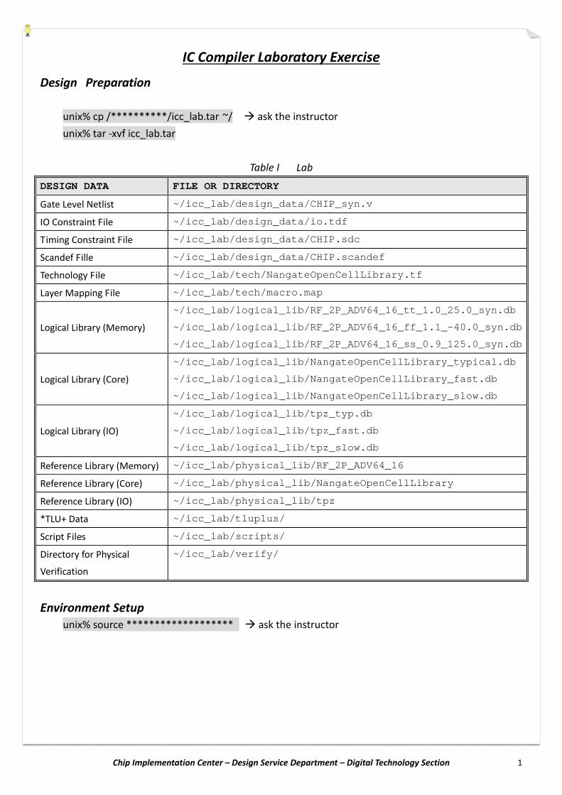
IC Compiler Laboratory Exercise
Design Preparation
unix% cp /**********/icc_lab.tar ~/ ask the instructor
unix% tar ‐xvf icc_lab.tar
Table I Lab
DESIGN DATA FILE OR DIRECTORY
Gate Level Netlist ~/icc_lab/design_data/CHIP_syn.v
IO Constraint File ~/icc_lab/design_data/io.tdf
Timing Constraint File ~/icc_lab/design_data/CHIP.sdc
Scandef Fille ~/icc_lab/design_data/CHIP.scandef
Technology File ~/icc_lab/tech/NangateOpenCellLibrary.tf
Layer Mapping File ~/icc_lab/tech/macro.map
Logical Library (Memory)
~/icc_lab/logical_lib/RF_2P_ADV64_16_tt_1.0_25.0_syn.db
~/icc_lab/logical_lib/RF_2P_ADV64_16_ff_1.1_-40.0_syn.db
~/icc_lab/logical_lib/RF_2P_ADV64_16_ss_0.9_125.0_syn.db
Logical Library (Core)
~/icc_lab/logical_lib/NangateOpenCellLibrary_typical.db
~/icc_lab/logical_lib/NangateOpenCellLibrary_fast.db
~/icc_lab/logical_lib/NangateOpenCellLibrary_slow.db
Logical Library (IO)
~/icc_lab/logical_lib/tpz_typ.db
~/icc_lab/logical_lib/tpz_fast.db
~/icc_lab/logical_lib/tpz_slow.db
Reference Library (Memory) ~/icc_lab/physical_lib/RF_2P_ADV64_16
Reference Library (Core) ~/icc_lab/physical_lib/NangateOpenCellLibrary
Reference Library (IO) ~/icc_lab/physical_lib/tpz
*TLU+ Data ~/icc_lab/tluplus/
Script Files ~/icc_lab/scripts/
Directory for Physical
Verification
~/icc_lab/verify/
Environment Setup unix% source ******************* ask the instructor
Chip Implementation Center – Design Service Department – Digital Technology Section 2
Lab1 Design Setup
1. Change directory to ~/run and invoke IC Compiler
unix% cd ~/icc_lab/run
unix% icc_shell –gui&
2. “ File > Create Library ”
在Input reference libraries項目點選視窗 Add
在Select Directory視窗選擇 ../physical_lib/NangateOpenCellLibrary 按 OK
../ physical_lib /RF_2P_ADV64_16 按 OK
../ physical_lib /tpz 按 OK 選擇完成。
按OK關閉視窗。
3. “ File > Import Designs ”
點選視窗 Add
在Select File視窗選擇 ../design_data/CHIP_syn.v 按 Open 選擇。
按OK。
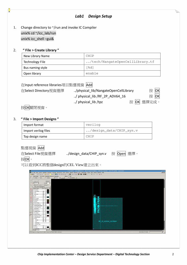
可以看到ICC將整個design的CEL View建立出來。
New Library Name CHIP
Technology File ../tech/NangateOpenCellLibrary.tf
Bus naming style [%d]
Open library enable
Import format verilog
Import verilog files ../design_data/CHIP_syn.v
Top design name CHIP
Chip Implementation Center – Design Service Department – Digital Technology Section 3
4. “ File > Set TLU+… ”
Max TLU+ file ../tluplus/NangateOpenCellLibrary.tluplus
Layer name mapping file between
technology library and ITF file ../tluplus/NangateOpenCellLibrary.map
5. “ File > Import >Read SDC…”
Input file name ../design_data/CHIP.sdc
Version Latest
Other default value
6. “ File > Save Design ”
點選Save All
“ File > Save Design ”
點選Show advanced options
Save As Enable
Save As Name design_setup
按OK。
7. “ File > Close Design ”
“ File > Close Library ”
※若 lab1無法完成,可在Message/Input Area輸入 source “../scripts/01_design_setup.tcl” 以
利後面的 lab進行。
p.s. 執行前請先將 CHIP 資料夾刪除(在 Terminal利用 rm –rf * 指令)
Chip Implementation Center – Design Service Department – Digital Technology Section 4
Lab2 Design Planning
1. Invoke IC Compiler (@path “~/icc_lab/run “)
unix% icc_shell –gui&
2. “ File > Open Library”
Library Name CHIP
open library as read‐only disable
open reference library for writing disable
按 OK。
“ File > Open Design”
選擇 CHIP
按 OK。
3. 我們要加入 IO及 Core 的 P/G pad, POC pad 及 Corner pad
在Message/Input Area輸入
source ../scripts/create_phy_cell.tcl
按 enter。
4. Read TDF file,先切換至 LayoutWindows
“ Floorplan > Read Pin/Pad Physical Constraints ”
Input file name ../design_data/io.tdf
按 OK。
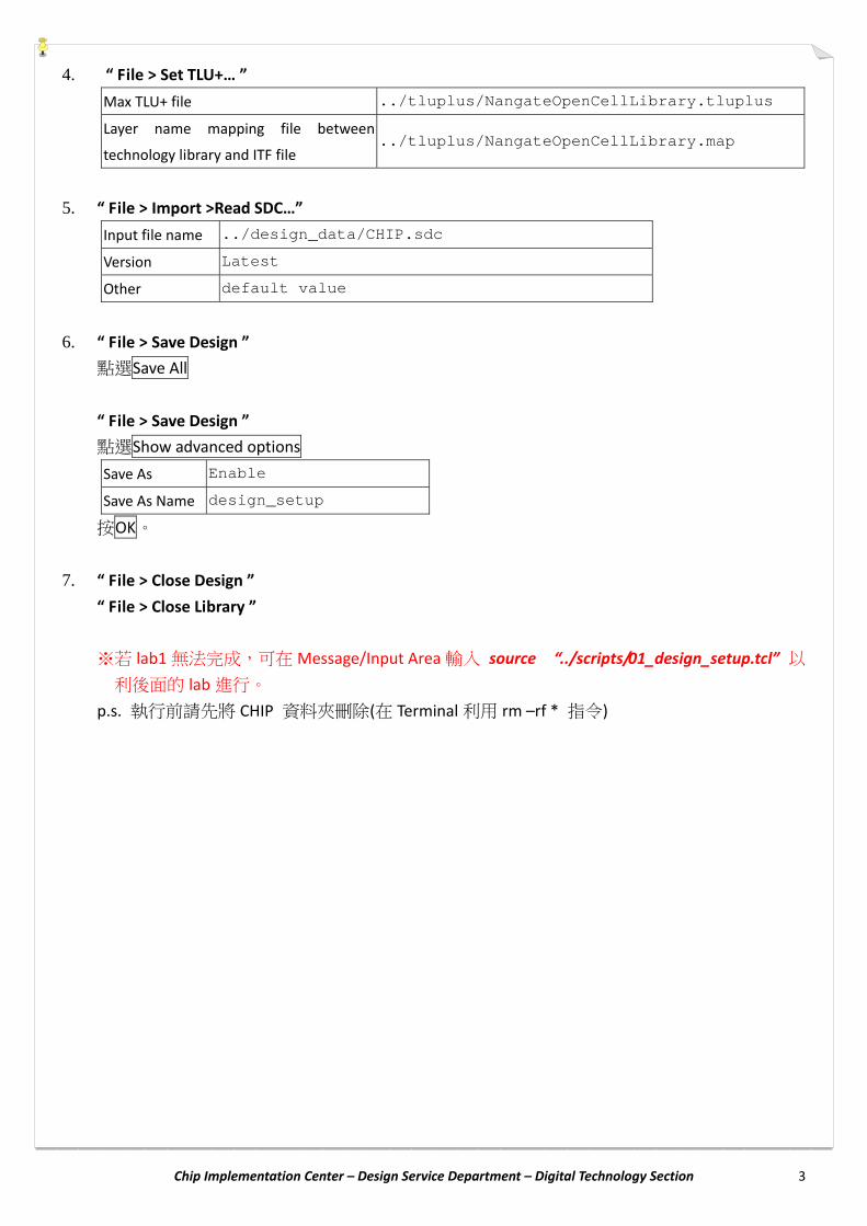
“ Floorplan > Create Floorplan… ”
Control type Aspect ratio
Core utilization 0.4
Aspect ratio (H/W) 1
Horizontal row Enable
Double back Enable
Start first row Disable
Flip first row Enable
Core to left 80
Core to bottom 80
Core to right 80
Core to top 80
按 OK。
Chip Implementation Center – Design Service Department – Digital Technology Section 5
5. Insert pad filler
“ Finishing > Insert Pad Filler ”
Pin/Blockage cells PADFILLER20 PADFILLER10 \
PADFILLER5 PADFILLER1 \
PADFILLER05 PADFILLER0005 (由大至小排序)
Pin/Blockage overlap cells PADFILLER0005
Boundary placement (Top) Enable
Boundary placement (Bottom) Enable
Boundary placement (Left) Enable
Boundary placement (Right) Enable
Other Default value
按 OK。
6. “ File > Save Design ”
點選 Save All
Chip Implementation Center – Design Service Department – Digital Technology Section 6
“ File > Save Design ”
點選Show advanced options
Save As Enable
Save As Name die_init
按OK。
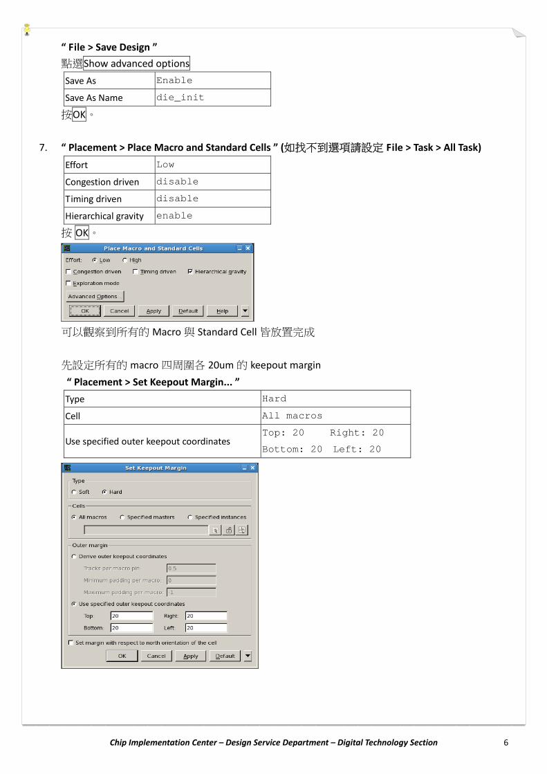
7. “ Placement > Place Macro and Standard Cells ” (如找不到選項請設定 File > Task > All Task)
Effort Low
Congestion driven disable
Timing driven disable
Hierarchical gravity enable
按 OK。
可以觀察到所有的Macro與 Standard Cell 皆放置完成
先設定所有的 macro四周圍各 20um的 keepout margin
“ Placement > Set Keepout Margin... ”
Type Hard
Cell All macros
Use specified outer keepout coordinates Top: 20 Right: 20
Bottom: 20 Left: 20
Chip Implementation Center – Design Service Department – Digital Technology Section 7
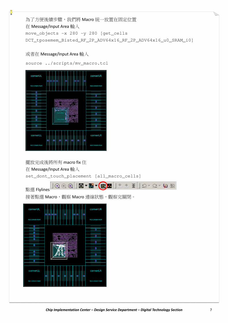
為了方便後續步驟,我們將Macro統一放置在固定位置
在Message/Input Area輸入
move_objects -x 280 -y 280 [get_cells
DCT_tposemem_Bisted_RF_2P_ADV64x16_RF_2P_ADV64x16_u0_SRAM_i0]
或者在Message/Input Area輸入
source ../scripts/mv_macro.tcl
擺放完成後將所有 macro fix 住
在Message/Input Area輸入
set_dont_touch_placement [all_macro_cells]
點選 Flylines
接著點選Macro,觀察Macro連線狀態,觀察完關閉。
Chip Implementation Center – Design Service Department – Digital Technology Section 8
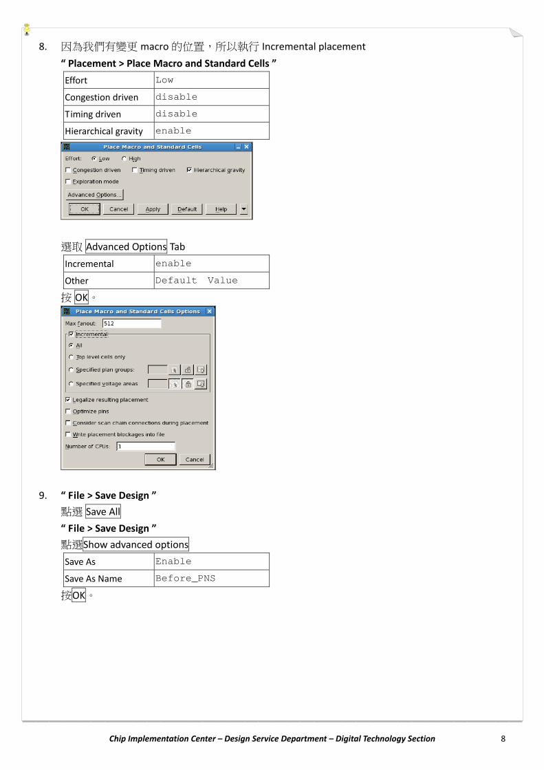
8. 因為我們有變更 macro的位置,所以執行 Incremental placement
“ Placement > Place Macro and Standard Cells ”
Effort Low
Congestion driven disable
Timing driven disable
Hierarchical gravity enable
選取 Advanced Options Tab
Incremental enable
Other Default Value
按 OK。
9. “ File > Save Design ”
點選 Save All
“ File > Save Design ”
點選Show advanced options
Save As Enable
Save As Name Before_PNS
按OK。
Chip Implementation Center – Design Service Department – Digital Technology Section 9
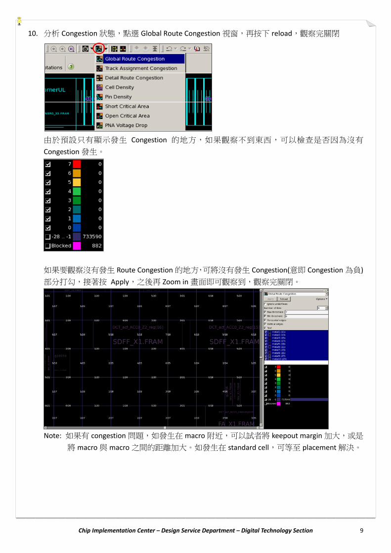
10. 分析 Congestion 狀態,點選 Global Route Congestion 視窗,再按下 reload,觀察完關閉
由於預設只有顯示發生 Congestion 的地方,如果觀察不到東西,可以檢查是否因為沒有
Congestion 發生。
如果要觀察沒有發生 Route Congestion的地方,可將沒有發生 Congestion(意即 Congestion為負)
部分打勾,接著按 Apply,之後再 Zoom in 畫面即可觀察到,觀察完關閉。
Note: 如果有 congestion問題,如發生在 macro附近,可以試者將 keepout margin加大,或是
將 macro與 macro之間的距離加大。如發生在 standard cell,可等至 placement解決。
Chip Implementation Center – Design Service Department – Digital Technology Section 10
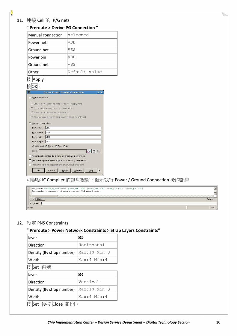
11. 連接 Cell 的 P/G nets
“ Preroute > Derive PG Connection ”
Manual connection selected
Power net VDD
Ground net VSS
Power pin VDD
Ground net VSS
Other Default value
按 Apply
按OK。
可觀察 IC Compiler的訊息視窗,顯示執行 Power / Ground Connection後的訊息
12. 設定 PNS Constraints
“ Preroute > Power Network Constraints > Strap Layers Constraints”
layer M5
Direction Horizontal
Density (By strap number) Max:10 Min:3
Width Max:4 Min:4
按 Set 再選
layer M4
Direction Vertical
Density (By strap number) Max:10 Min:3
Width Max:4 Min:4
按 Set 後按 Close 離開。
Chip Implementation Center – Design Service Department – Digital Technology Section 11
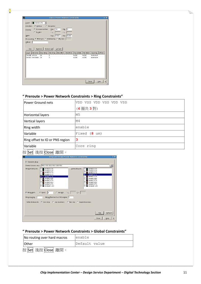
“ Preroute > Power Network Constraints > Ring Constraints”
Power Ground nets VDD VSS VDD VSS VDD VSS
(6圈共 3對)
Horizontal layers M5
Vertical layers M4
Ring width enable
Variable Fixed (8 um)
Ring offset to IO or PNS region 3
Variable Core ring
按 Set 後按 Close 離開。
“ Preroute > Power Network Constraints > Global Constraints”
No routing over hard macros enable
Other Default value
按 Set 後按 Close 離開。
Chip Implementation Center – Design Service Department – Digital Technology Section 12
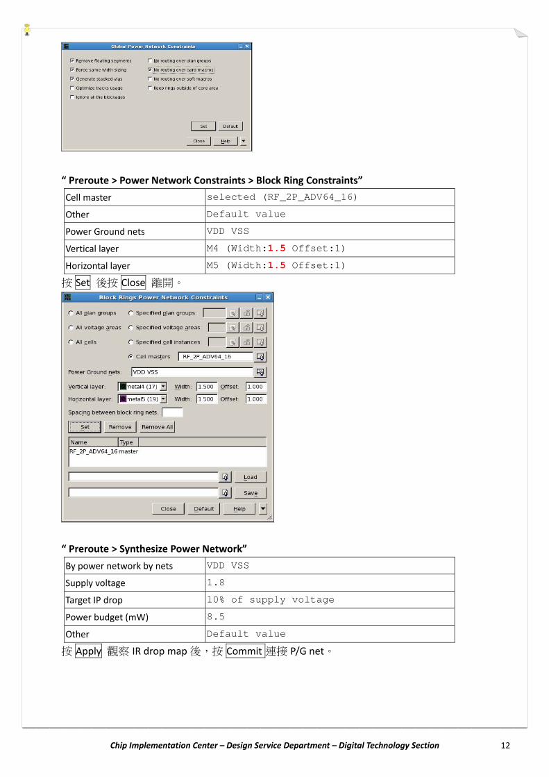
“ Preroute > Power Network Constraints > Block Ring Constraints”
Cell master selected (RF_2P_ADV64_16)
Other Default value
Power Ground nets VDD VSS
Vertical layer M4 (Width:1.5 Offset:1)
Horizontal layer M5 (Width:1.5 Offset:1)
按 Set 後按 Close 離開。
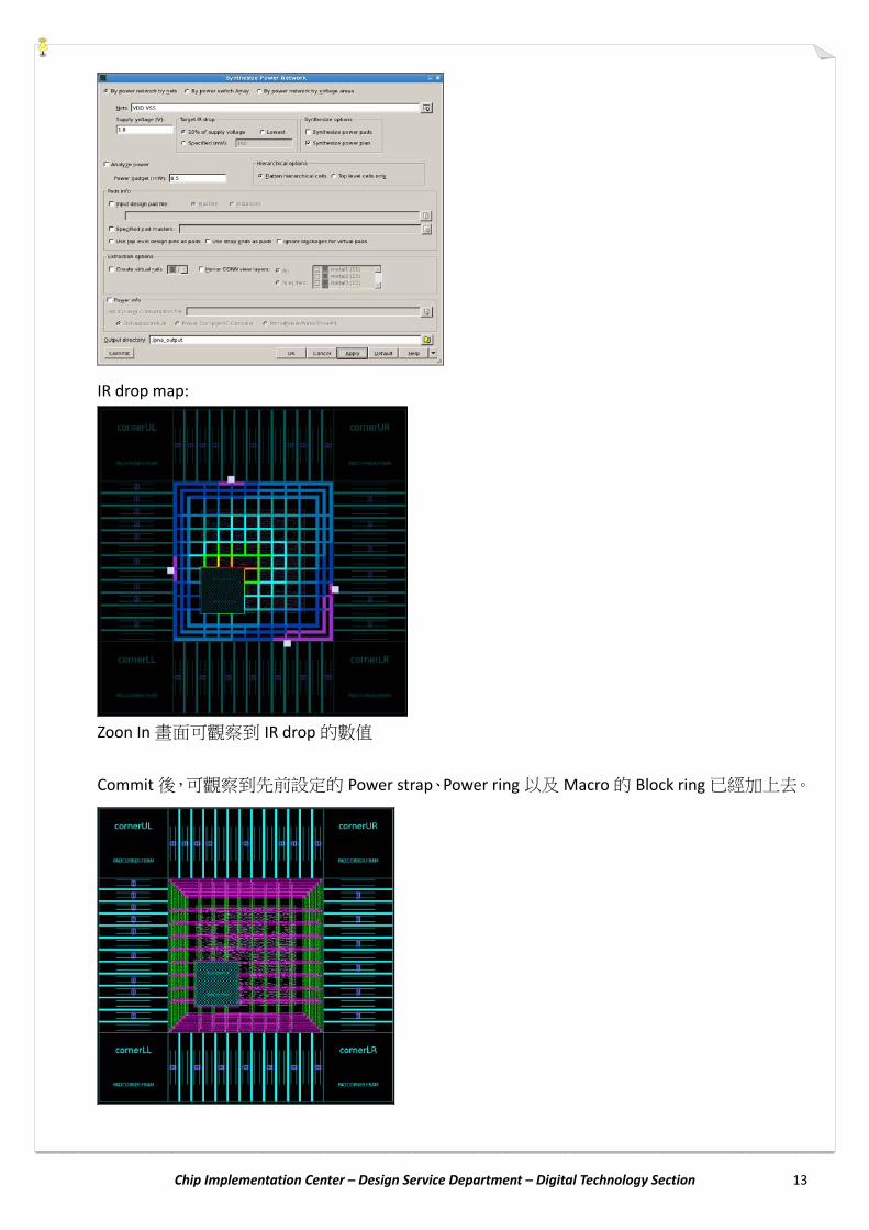
“ Preroute > Synthesize Power Network”
By power network by nets VDD VSS
Supply voltage 1.8
Target IP drop 10% of supply voltage
Power budget (mW) 8.5
Other Default value
按 Apply 觀察 IR drop map後,按 Commit 連接 P/G net。
Chip Implementation Center – Design Service Department – Digital Technology Section 13
IR drop map:
Zoon In畫面可觀察到 IR drop的數值
Commit後,可觀察到先前設定的 Power strap、Power ring以及Macro的 Block ring已經加上去。
Chip Implementation Center – Design Service Department – Digital Technology Section 14
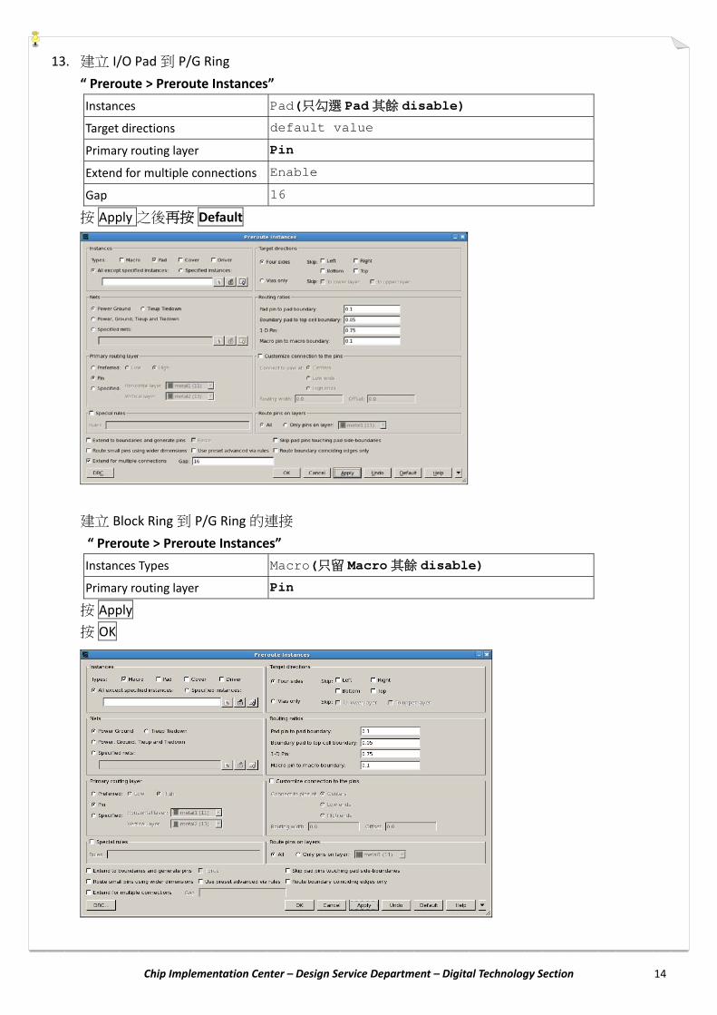
13. 建立 I/O Pad到 P/G Ring
“ Preroute > Preroute Instances”
Instances Pad(只勾選 Pad其餘 disable)
Target directions default value
Primary routing layer Pin
Extend for multiple connections Enable
Gap 16
按 Apply 之後再按 Default
建立 Block Ring到 P/G Ring的連接
“ Preroute > Preroute Instances”
按 Apply
按 OK
Instances Types Macro(只留 Macro其餘 disable)
Primary routing layer Pin
Chip Implementation Center – Design Service Department – Digital Technology Section 15
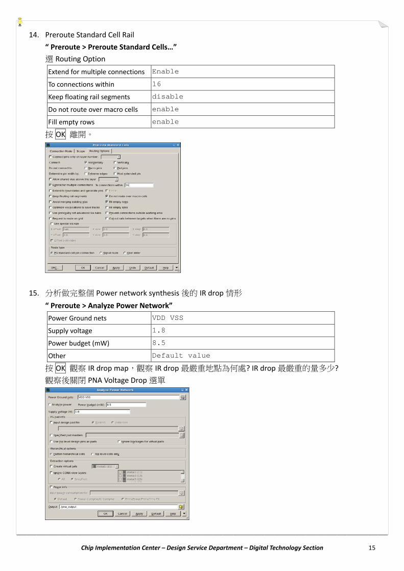
14. Preroute Standard Cell Rail
“ Preroute > Preroute Standard Cells…”
選 Routing Option
Extend for multiple connections Enable
To connections within 16
Keep floating rail segments disable
Do not route over macro cells enable
Fill empty rows enable
按 OK 離開。
15. 分析做完整個 Power network synthesis後的 IR drop情形
“ Preroute > Analyze Power Network”
Power Ground nets VDD VSS
Supply voltage 1.8
Power budget (mW) 8.5
Other Default value
按 OK 觀察 IR drop map,觀察 IR drop最嚴重地點為何處? IR drop最嚴重的量多少?
觀察後關閉 PNA Voltage Drop選單
Chip Implementation Center – Design Service Department – Digital Technology Section 16
16. 設定 Strap下不要擺放 Standard Cell
在Message/Input Area輸入
set_pnet_options -partial "metal4 metal5"
create_fp_placement -incremental all
17. “ File > Save Design ”
點選 Save All
“ File > Save Design ”
點選Show advanced options
Save As Enable
Save As Name design_planning
按OK。
18. “ File > Close Design ”
“ File > Close Library ”
※若 lab2無法完成,可在Message/Input Area輸入 source “../scripts/02_design_planning.tcl”
以利後面的 lab進行。
Chip Implementation Center – Design Service Department – Digital Technology Section 17
Lab3 Placement 1. Invoke IC Compiler
unix% icc_shell –gui&
2. “ File > Open Library”
Library Name CHIP
open library as read‐only disable
open reference library for writing disable
按 OK。
“ File > Open Design”
選擇 CHIP
按 OK。
3. “ File > Import >Read SDC…”
Input file name ../design_data/CHIP.sdc
Version Latest
Other default value
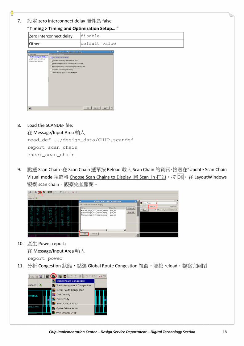
4. 設定 zero interconnect delay 屬性為 true
“Timing > Timing and Optimization Setup… ”
Zero Interconnect delay enable
Other default value
5. Report timing
在Message/Input Area輸入
report_timing
6. Check all constraint violations:
在Message/Input Area輸入
report_constraint –all
Chip Implementation Center – Design Service Department – Digital Technology Section 18
7. 設定 zero interconnect delay 屬性為 false
“Timing > Timing and Optimization Setup… ”
Zero Interconnect delay disable
Other default value
8. Load the SCANDEF file:
在Message/Input Area輸入
read_def ../design_data/CHIP.scandef
report_scan_chain
check_scan_chain
9. 點選 Scan Chain,在 Scan Chain選單按 Reload載入 Scan Chain的資訊,接著在”Update Scan Chain
Visual mode視窗將 Choose Scan Chains to Display 將 Scan_In打勾,按 OK。在 LayoutWindows
觀察 scan chain,觀察完並關閉。
10. 產生 Power report:
在Message/Input Area輸入
report_power
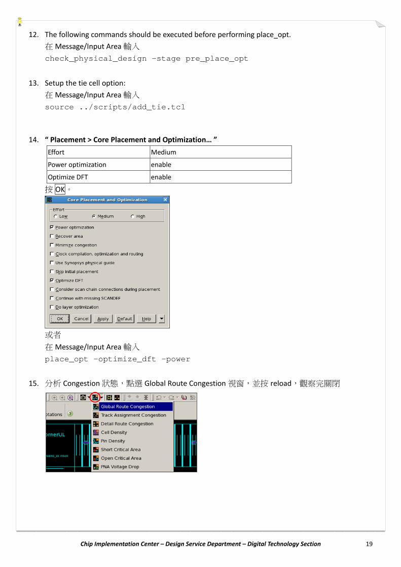
11. 分析 Congestion 狀態,點選 Global Route Congestion 視窗,並按 reload,觀察完關閉
Chip Implementation Center – Design Service Department – Digital Technology Section 19
12. The following commands should be executed before performing place_opt.
在Message/Input Area輸入
check_physical_design –stage pre_place_opt
13. Setup the tie cell option:
在Message/Input Area輸入
source ../scripts/add_tie.tcl
14. “ Placement > Core Placement and Optimization… ”
Effort Medium
Power optimization enable
Optimize DFT enable
按 OK。
或者
在Message/Input Area輸入
place_opt -optimize_dft -power
15. 分析 Congestion 狀態,點選 Global Route Congestion 視窗,並按 reload,觀察完關閉
Chip Implementation Center – Design Service Department – Digital Technology Section 20
16. Report timing
在Message/Input Area輸入
report_timing
Note: 如果有 timing問題請下 place_opt
如果有 congestion問題,請參考講義第 4-63頁流程
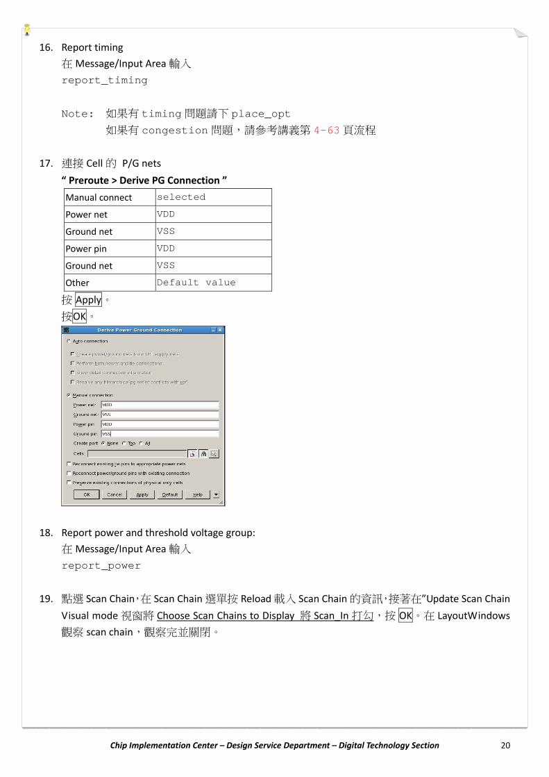
17. 連接 Cell 的 P/G nets
“ Preroute > Derive PG Connection ”
Manual connect selected
Power net VDD
Ground net VSS
Power pin VDD
Ground net VSS
Other Default value
按 Apply。
按OK。
18. Report power and threshold voltage group:
在Message/Input Area輸入
report_power
19. 點選 Scan Chain,在 Scan Chain選單按 Reload載入 Scan Chain的資訊,接著在”Update Scan Chain
Visual mode視窗將 Choose Scan Chains to Display 將 Scan_In打勾,按 OK。在 LayoutWindows
觀察 scan chain,觀察完並關閉。
Chip Implementation Center – Design Service Department – Digital Technology Section 21
20. “ File > Save Design
點選 Save All
“ File > Save Design ”
點選Show advanced options
Save As Enable
Save As Name placement
按 OK。
21. “ File > Close Design ”
“ File > Close Library ”
※若 lab3無法完成,可在Message/Input Area輸入 source “../scripts/03_placement.tcl” 以利
後面的 lab進行。
Chip Implementation Center – Design Service Department – Digital Technology Section 22
Lab4 CTS 1. Invoke IC Compiler
unix% icc_shell –gui&
2. “ File > Open Library”
Library Name CHIP
open library as read‐only disable
open reference library for writing disable
按 OK。
“ File > Open Design”
選擇 CHIP
按 OK。
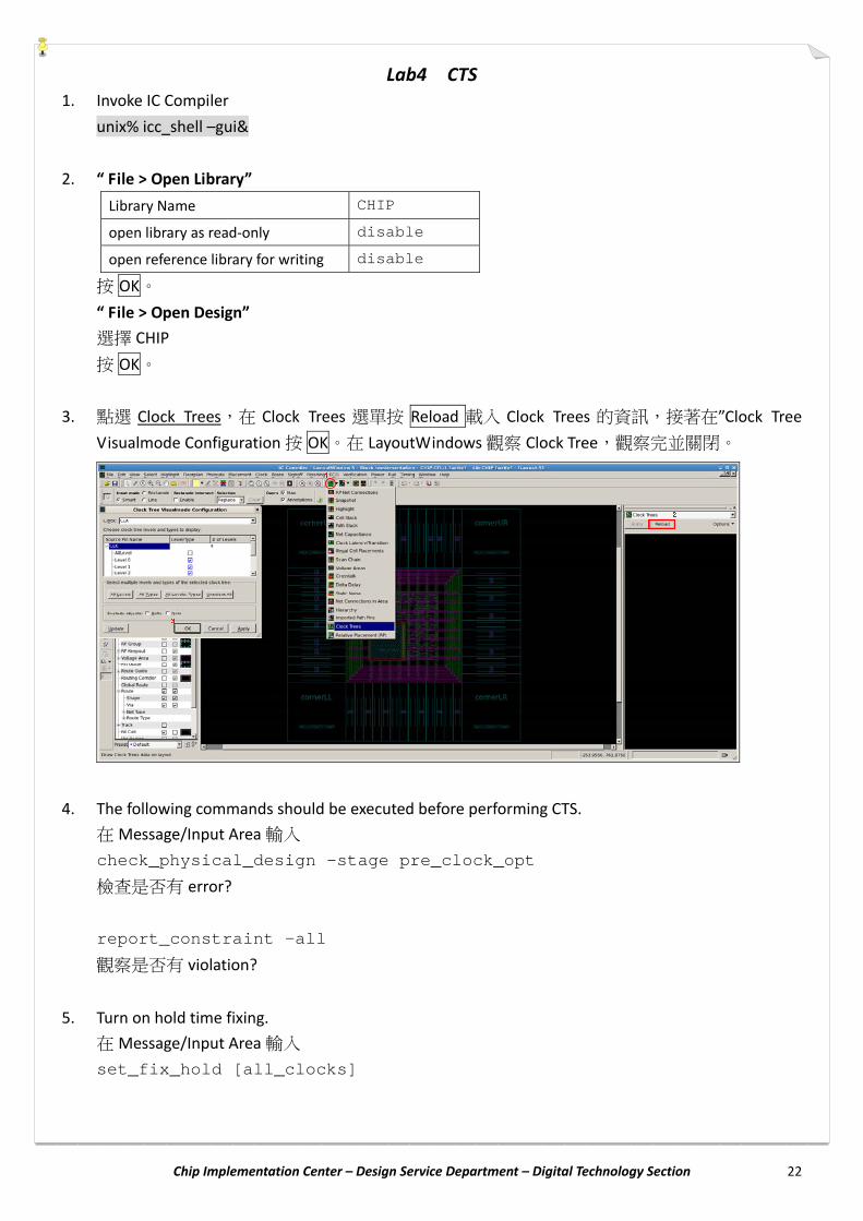
3. 點選 Clock Trees,在 Clock Trees 選單按 Reload 載入 Clock Trees 的資訊,接著在”Clock Tree
Visualmode Configuration 按 OK。在 LayoutWindows觀察 Clock Tree,觀察完並關閉。
4. The following commands should be executed before performing CTS.
在Message/Input Area輸入
check_physical_design –stage pre_clock_opt
檢查是否有 error?
report_constraint -all
觀察是否有 violation?
5. Turn on hold time fixing.
在Message/Input Area輸入
set_fix_hold [all_clocks]
Chip Implementation Center – Design Service Department – Digital Technology Section 23
6. Report timing
在Message/Input Area輸入
report_timing
7. Perform CTS optmization:
在Message/Input Area輸入
clock_opt -fix_hold_all_clocks -no_clock_route
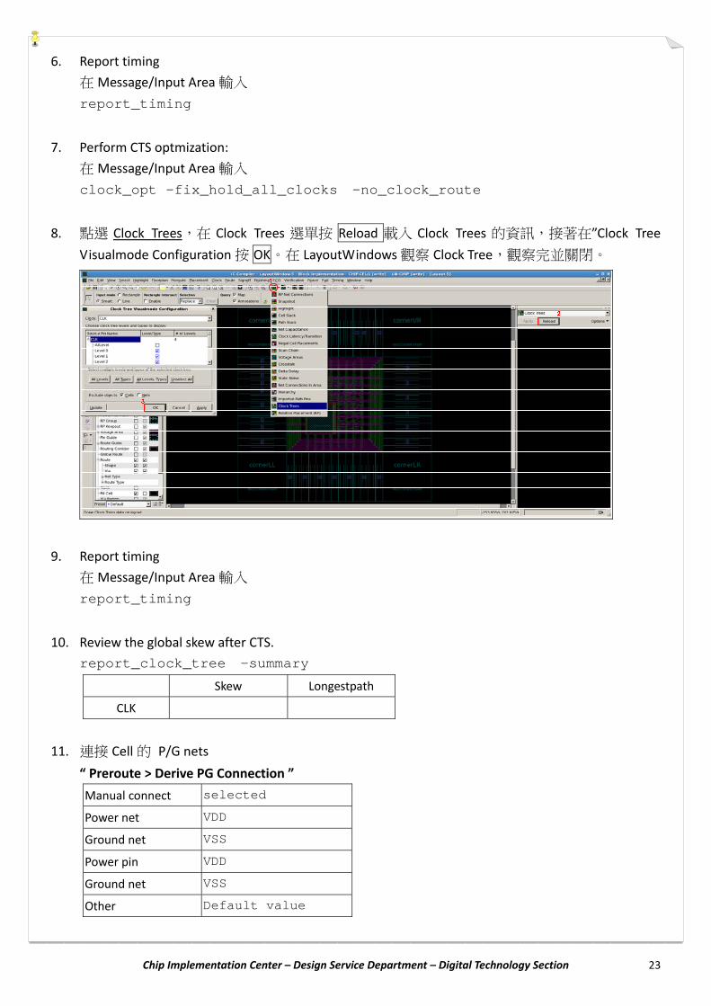
8. 點選 Clock Trees,在 Clock Trees 選單按 Reload 載入 Clock Trees 的資訊,接著在”Clock Tree
Visualmode Configuration 按 OK。在 LayoutWindows觀察 Clock Tree,觀察完並關閉。
9. Report timing
在Message/Input Area輸入
report_timing
10. Review the global skew after CTS.
report_clock_tree -summary
Skew Longestpath
CLK
11. 連接 Cell 的 P/G nets
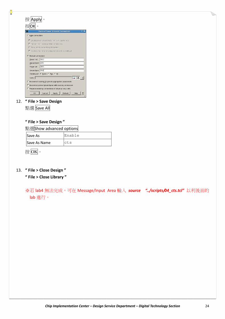
“ Preroute > Derive PG Connection ”
Manual connect selected
Power net VDD
Ground net VSS
Power pin VDD
Ground net VSS
Other Default value
Chip Implementation Center – Design Service Department – Digital Technology Section 24
按 Apply。
按OK。
12. “ File > Save Design
點選 Save All
“ File > Save Design ”
點選Show advanced options
Save As Enable
Save As Name cts
按 OK。
13. “ File > Close Design ”
“ File > Close Library ”
※若 lab4 無法完成,可在Message/Input Area輸入 source “../scripts/04_cts.tcl” 以利後面的
lab進行。
Chip Implementation Center – Design Service Department – Digital Technology Section 25
Lab5 Route 1. Invoke IC Compiler
unix% icc_shell –gui&
2. “ File > Open Library”
Library Name CHIP
open library as read‐only disable
open reference library for writing disable
按 OK。
“ File > Open Design”
選擇 CHIP
按 OK。
3. Analyze the design for timing (setup and hold)
在Message/Input Area輸入
report_timing
觀察 Timing有無 violation?
4. Check the routeability of the design
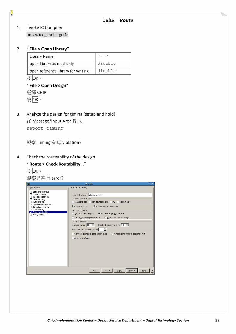
“ Route > Check Routability…”
按 OK。
觀察是否有 error?
Chip Implementation Center – Design Service Department – Digital Technology Section 26
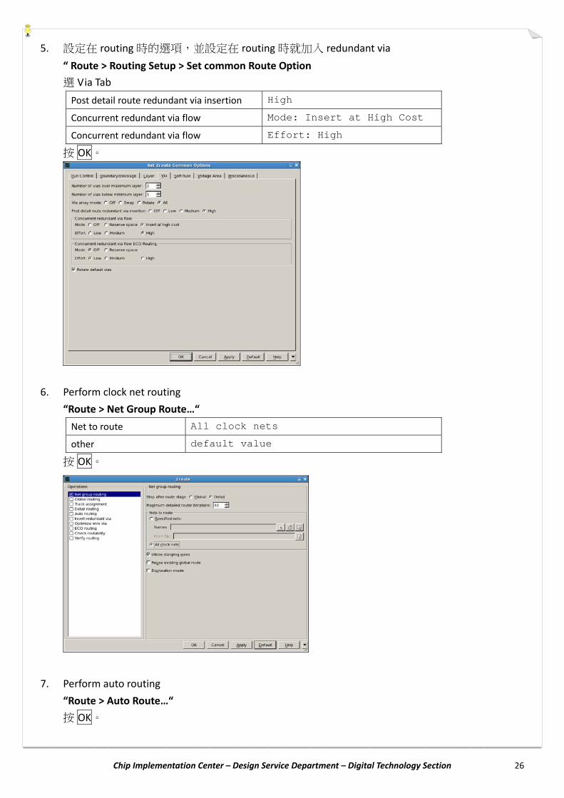
5. 設定在 routing時的選項,並設定在 routing時就加入 redundant via
“ Route > Routing Setup > Set common Route Option
選 Via Tab
Post detail route redundant via insertion High
Concurrent redundant via flow Mode: Insert at High Cost
Concurrent redundant via flow Effort: High
按 OK。
6. Perform clock net routing
“Route > Net Group Route…“
Net to route All clock nets
other default value
按 OK。
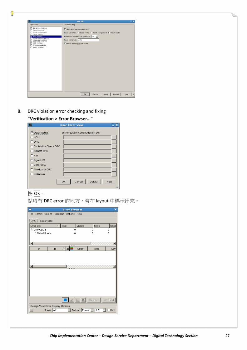
7. Perform auto routing
“Route > Auto Route…“
按 OK。
Chip Implementation Center – Design Service Department – Digital Technology Section 27
8. DRC violation error checking and fixing
“Verification > Error Browser…”
按 OK。
點取有 DRC error的地方,會在 layout中標示出來。
Chip Implementation Center – Design Service Department – Digital Technology Section 28
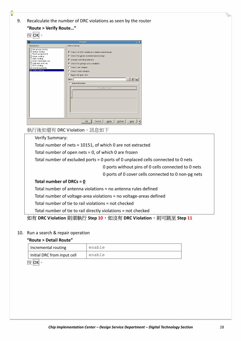
9. Recalculate the number of DRC violations as seen by the router
“Route > Verify Route…”
按 OK。
執行後如還有 DRC Violation,訊息如下
Verify Summary:
Total number of nets = 10151, of which 0 are not extracted
Total number of open nets = 0, of which 0 are frozen
Total number of excluded ports = 0 ports of 0 unplaced cells connected to 0 nets
0 ports without pins of 0 cells connected to 0 nets
0 ports of 0 cover cells connected to 0 non‐pg nets
Total number of DRCs = 0
Total number of antenna violations = no antenna rules defined
Total number of voltage‐area violations = no voltage‐areas defined
Total number of tie to rail violations = not checked
Total number of tie to rail directly violations = not checked
如有 DRC Violation則須執行 Step 10,如沒有 DRC Violation,則可跳至 Step 11
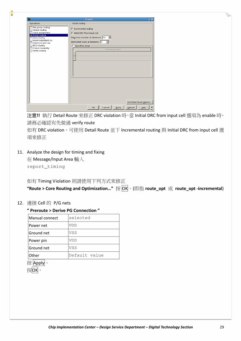
10. Run a search & repair operation
“Route > Detail Route”
Incremental routing enable
Initial DRC from input cell enable
按 OK。
Chip Implementation Center – Design Service Department – Digital Technology Section 29
注意!! 執行 Detail Route來修正 DRC violation時,當 Initial DRC from input cell選項為 enable時,
請務必確認有先做過 verify route
如有 DRC violation,可使用 Detail Route 並下 Incremental routing與 Initial DRC from input cell 選
項來修正
11. Analyze the design for timing and fixing
在Message/Input Area輸入
report_timing
如有 Timing Violation 則請使用下列方式來修正
“Route > Core Routing and Optimization…” 按 OK。(即指 route_opt 或 route_opt ‐incremental)
12. 連接 Cell 的 P/G nets
“ Preroute > Derive PG Connection ”
Manual connect selected
Power net VDD
Ground net VSS
Power pin VDD
Ground net VSS
Other Default value
按 Apply。
按OK。
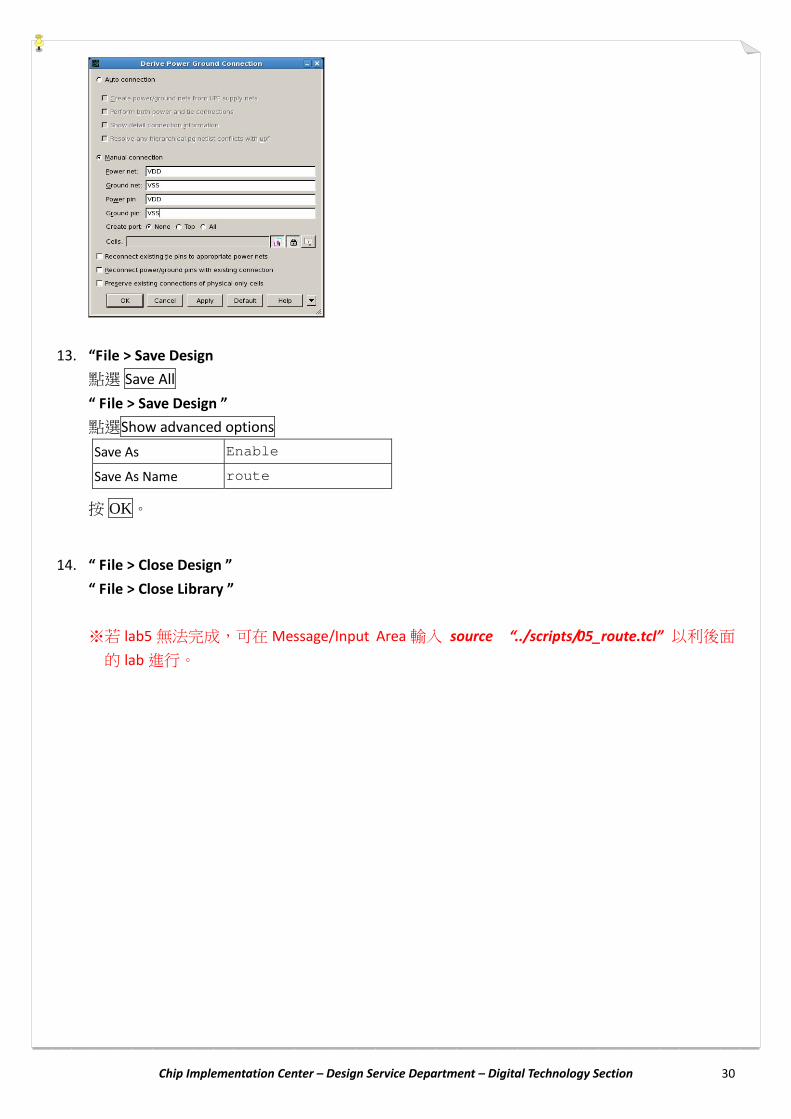
Chip Implementation Center – Design Service Department – Digital Technology Section 30
13. “File > Save Design
點選 Save All
“ File > Save Design ”
點選Show advanced options
Save As Enable
Save As Name route
按 OK。
14. “ File > Close Design ”
“ File > Close Library ”
※若 lab5無法完成,可在Message/Input Area輸入 source “../scripts/05_route.tcl” 以利後面
的 lab進行。
Chip Implementation Center – Design Service Department – Digital Technology Section 31
Lab6 DFM 1. Invoke IC Compiler
unix% icc_shell ‐gui&
2. “ File > Open Library”
Library Name CHIP
open library as read‐only disable
open reference library for writing disable
按 OK。
“ File > Open Design”
選擇 CHIP
按 OK。
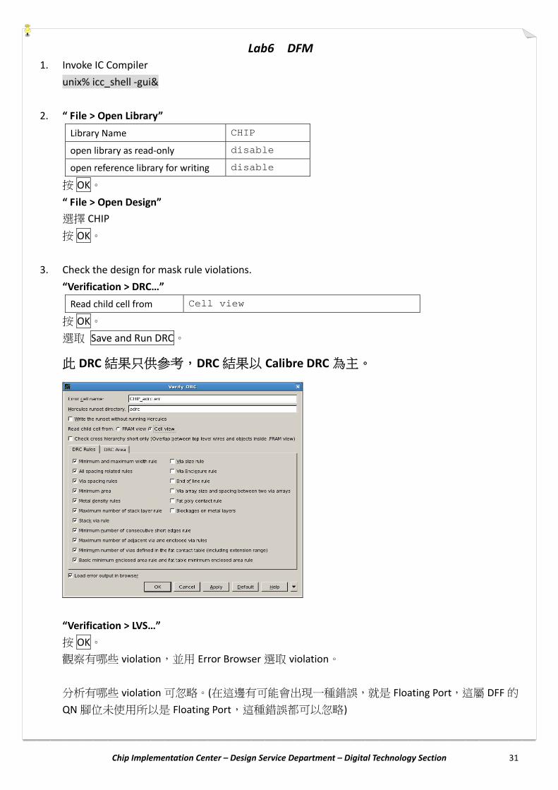
3. Check the design for mask rule violations.
“Verification > DRC…”
Read child cell from Cell view
按 OK。
選取 Save and Run DRC。
此 DRC結果只供參考,DRC 結果以 Calibre DRC 為主。
“Verification > LVS…”
按 OK。
觀察有哪些 violation,並用 Error Browser選取 violation。
分析有哪些 violation 可忽略。(在這邊有可能會出現一種錯誤,就是 Floating Port,這屬 DFF的
QN腳位未使用所以是 Floating Port,這種錯誤都可以忽略)
Chip Implementation Center – Design Service Department – Digital Technology Section 32
4. Insert standard cell filler
在Message/Input Area輸入
source ../scripts/addCoreFiller.cmd
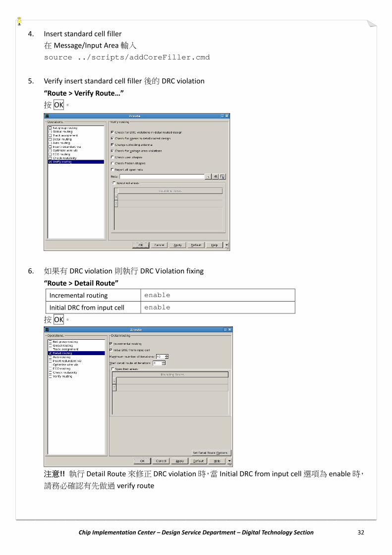
5. Verify insert standard cell filler 後的 DRC violation
“Route > Verify Route…”
按 OK。
6. 如果有 DRC violation 則執行 DRC Violation fixing
“Route > Detail Route”
Incremental routing enable
Initial DRC from input cell enable
按 OK。
注意!! 執行 Detail Route來修正 DRC violation時,當 Initial DRC from input cell選項為 enable時,
請務必確認有先做過 verify route
Chip Implementation Center – Design Service Department – Digital Technology Section 33
7. Analyze the design for timing and fixing
在Message/Input Area輸入
report_timing
但如果有 timing violation 時,則請使用下列方式來修正
“Route > Core routing and Optimization…” 按 OK。(即指 route_opt or route_opt ‐incremental)
8. 如有 Antenna Violation 則需插入 antenna diode,沒有即可跳過此步驟
先設定插入 antenna diode 的設定
“ Route > Routing Setup > Set Detail Route Options… ”
選擇 Antenna Tab
Diode library cells for antenna fixing ANTENNA_X1
Insert diode during routing to fix antenna violations enable
Other Default value
按 OK 離開。
再執行 Antenna Violation Fixing
“Route > Verify Route…”
按 OK。
“Route > Detail Route”
Incremental routing enable
Initial DRC from input cell enable
按 OK。
Chip Implementation Center – Design Service Department – Digital Technology Section 34
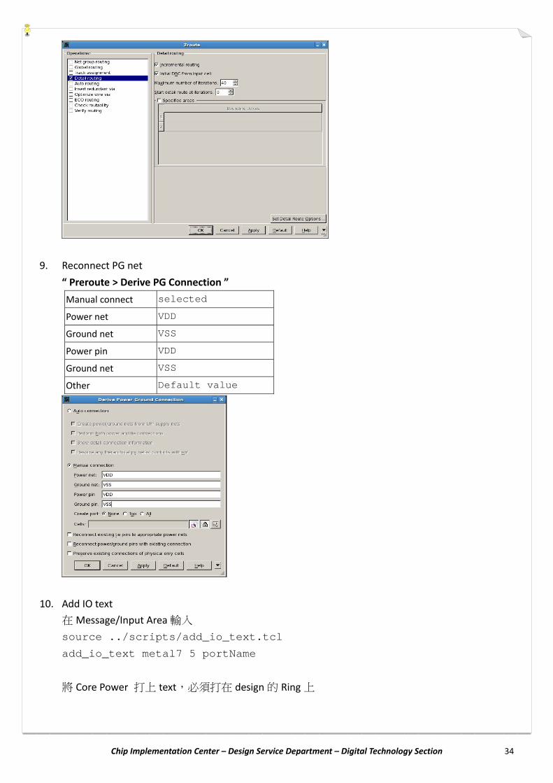
9. Reconnect PG net
“ Preroute > Derive PG Connection ”
Manual connect selected
Power net VDD
Ground net VSS
Power pin VDD
Ground net VSS
Other Default value
10. Add IO text
在Message/Input Area輸入
source ../scripts/add_io_text.tcl
add_io_text metal7 5 portName
將 Core Power 打上 text,必須打在 design的 Ring上
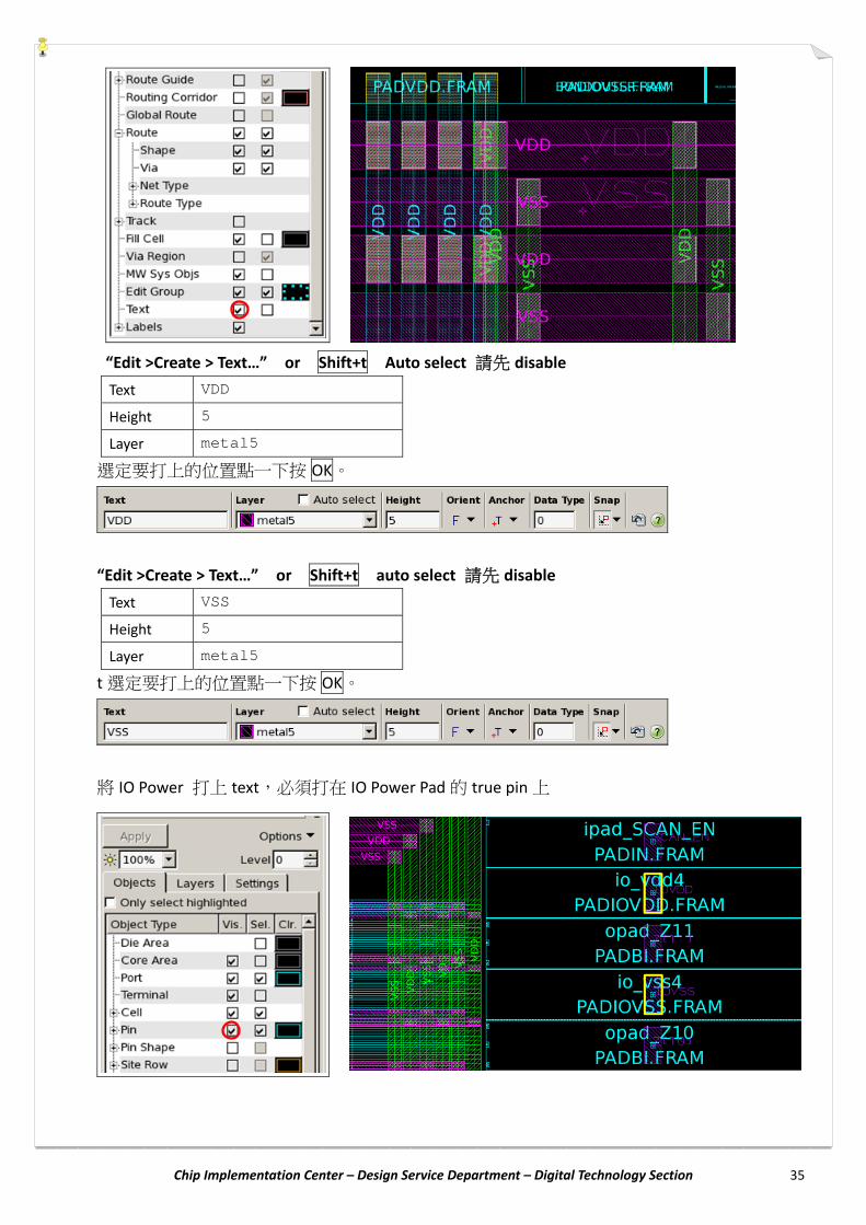
Chip Implementation Center – Design Service Department – Digital Technology Section 35
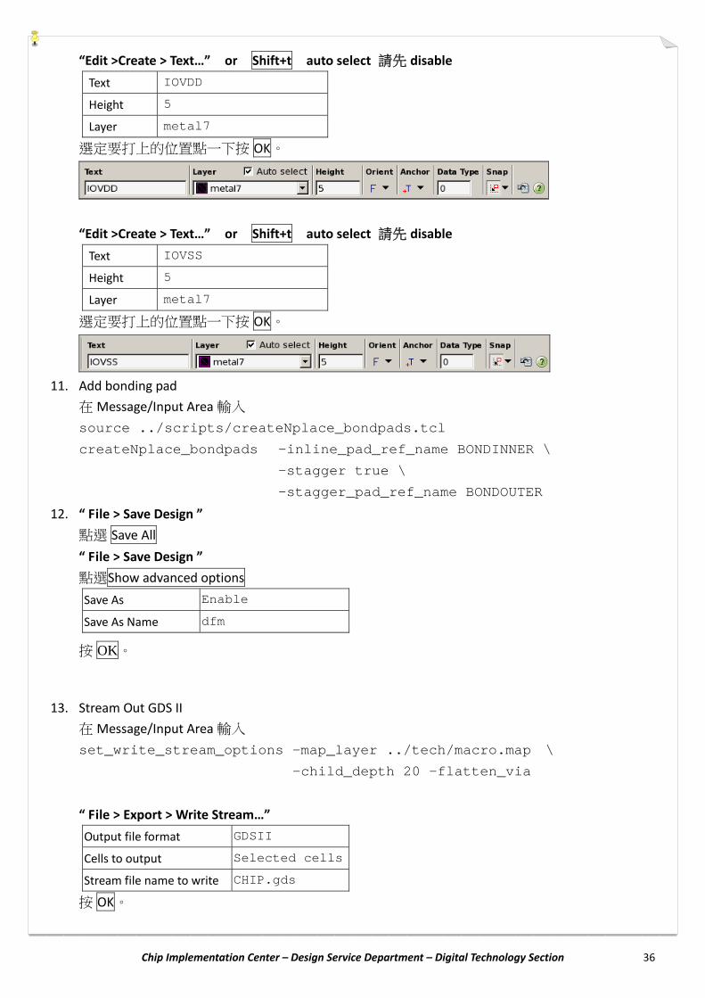
“Edit >Create > Text…” or Shift+t Auto select 請先 disable
Text VDD
Height 5
Layer metal5
選定要打上的位置點一下按 OK。
“Edit >Create > Text…” or Shift+t auto select 請先 disable
Text VSS
Height 5
Layer metal5
t選定要打上的位置點一下按 OK。
將 IO Power 打上 text,必須打在 IO Power Pad的 true pin上
Chip Implementation Center – Design Service Department – Digital Technology Section 36
“Edit >Create > Text…” or Shift+t auto select 請先 disable
Text IOVDD
Height 5
Layer metal7
選定要打上的位置點一下按 OK。
“Edit >Create > Text…” or Shift+t auto select 請先 disable
Text IOVSS
Height 5
Layer metal7
選定要打上的位置點一下按 OK。
11. Add bonding pad
在Message/Input Area輸入
source ../scripts/createNplace_bondpads.tcl
createNplace_bondpads -inline_pad_ref_name BONDINNER \
-stagger true \
-stagger_pad_ref_name BONDOUTER
12. “ File > Save Design ”
點選 Save All
“ File > Save Design ”
點選Show advanced options
Save As Enable
Save As Name dfm
按 OK。
13. Stream Out GDS II
在Message/Input Area輸入
set_write_stream_options -map_layer ../tech/macro.map \
-child_depth 20 -flatten_via
“ File > Export > Write Stream…”
Output file format GDSII
Cells to output Selected cells
Stream file name to write CHIP.gds
按 OK。
Chip Implementation Center – Design Service Department – Digital Technology Section 37
將 GDS檔 copy 至 verify資料夾內
unix% cp ./CHIP.gds ../verify/drc
unix% cp ./CHIP.gds ../verify/lvs
14. 輸出 SDF檔
在Message/Input Area輸入
write_sdf -version 1.0 -context verilog -load_delay net CHIP.sdf
15. Verilog Out for post‐layout simulation & LVS
“ File > Export > Write Verilog…”
先按 Default
Output verilog file name CHIP_route.v
Output physical only cells disable
Unconnected ports enable
Diode ports enable
Wire declaration enable
Backslash before Hierarchy Separator enable
按 OK
將 verilog檔 copy 至資料夾內
unix% cp ./CHIP_route.v ../verify/lvs
Chip Implementation Center – Design Service Department – Digital Technology Section 38
16. File > Save Design
點選 Save All
15. “ File > Close Design ”
“ File > Close Library ”
Chip Implementation Center – Design Service Department – Digital Technology Section 39
Lab7 Calibre DRC & LVS & Post‐Layout Simulation
1. Change directory to ~/icc_lab/verify/drc
unix% cd ~/icc_lab/verify/drc
2. 修改 calibreDRC.rul檔
LAYOUT PATH "./CHIP.gds"
LAYOUT PRIMARY "CHIP"
3. 執行 Calibre DRC
unix% calibre –drc –hier calibreDRC.rul
觀察 DRC.summary 檔看看是否有 drc error,應該會看到幾個 DRC error,所有的 density 相關
violation 都可以忽略,可以不予理會這個 DRC error
若有 error,利用 Calibre RVE 可找到 drc 錯誤的數量、原因、坐標等資訊,再回到 IC Compiler
去做修正。
unix% calibre –rve DRC.results
4. 在 ICC 讀入 Calibre DRC的結果
在 ICC Layout window 下
“ Verification > Read Third‐party DRC Error File…
Error file ../verify/drc/DRC.results
Other default value
觀察有 Violation 的地方在哪,以及有哪些是 ICC 沒看到而 Calibre DRC 有看到的 violation
5. Change directory to ~/icc_lab/verify/lvs
unix% cd ~/icc_lab/verify/lvs
6. 產生 RAM Black Box 的 Verilog和 Spice 檔
修改原來的 RF_2P_ADV64_16.v檔,只留下module和 input、output的宣告,如還有其他Memory
以此類推。
Chip Implementation Center – Design Service Department – Digital Technology Section 40
RF_2P_ADV64_16.v (已編輯完畢)
利用 v2lvs 產生 RF_2P_ADV64_16.spi檔(已產生)
unix% v2lvs –v RF_2P_ADV64_16.v –o RF_2P_ADV64_16.spi
RF_2P_ADV64_16.spi
$ Spice netlist generated by v2lvs
$ v2013.4_26.18
.SUBCKT RF_2P_ADV64_16 QA[15] QA[14] QA[13] QA[12] QA[11] QA[10] QA[9] QA[8]
VDD VSS
+ QA[7] QA[6] QA[5] QA[4] QA[3] QA[2] QA[1] QA[0] CLKA CENA AA[5] AA[4] AA[3]
+ AA[2] AA[1] AA[0] CLKB CENB AB[5] AB[4] AB[3] AB[2] AB[1] AB[0] DB[15] DB[14]
+ DB[13] DB[12] DB[11] DB[10] DB[9] DB[8] DB[7] DB[6] DB[5] DB[4] DB[3] DB[2]
+ DB[1] DB[0] EMAA[2] EMAA[1] EMAA[0] EMAB[2] EMAB[1] EMAB[0]
.ENDS
7. 修改 CHIP_route.v將所有 Power pad關鍵字註解
//PADIOVSS io_vss7 (.VSSIO (SYNOPSYS_UNCONNECTED_189));
//PADIOVDD io_vdd6 (.VDDIO (SYNOPSYS_UNCONNECTED_196));
//PADIOVDDPOC io_vdd7 (.VDDIO (SYNOPSYS_UNCONNECTED_202));
8. 將 CHIP_route.v轉換成 spice 格式
v2lvs ‐v ./CHIP_route.v ‐l NangateOpenCellLibrary_lvs.v ‐l RF_2P_ADV64_16_lvs.v ‐l tpz_lvs.v ‐s
NangateOpenCellLibrary_lvs.spi ‐s RF_2P_ADV64_16_lvs.spi ‐s tpz_lvs.spi ‐o CHIP.spi ‐s1 VDD ‐s0
VSS
或
unix% ./v2lvs_lab.sh
module RF_2P_ADV64_16(QA, CLKA, CENA, AA, CLKB, CENB, AB, DB, EMAA, EMAB);
output [15:0] QA;
input CLKA;
input CENA;
input [5:0] AA;
input CENB;
input [5:0] AB;
input [15:0] DB;
input [2:0] EMAA;
input [2:0] EMAB;
endmodule
Chip Implementation Center – Design Service Department – Digital Technology Section 41
9. 修改 calibreLVS.rul
LAYOUT PRIMARY "CHIP"
LAYOUT PATH "./CHIP.gds"
LAYOUT CASE YES(加上) Lab中已加入,請確認
SOURCE PRIMARY "CHIP"
SOURCE PATH "./CHIP.spi"
SOURCE CASE YES(加上) Lab中已加入,請確認
VIRTUAL CONNECT BOX NAME "?"(加上) Lab中已加入,請確認
移除 IO Power & Ground相關
//LVS BOX PADIOVDD
//LVS BOX PADIOVSS
//LVS BOX PADIOVDDPOC
移除 CORE Power & Ground相關
//LVS BOX PADVDD
//LVS BOX PADVSS
移除 FILL與 PADFILL 相關
//LVS BOX FILLCELL_X1
//LVS BOX FILLCELL_X2
//LVS BOX FILLCELL_X4
//LVS BOX FILLCELL_X8
//LVS BOX FILLCELL_X16
//LVS BOX FILLCELL_X32
//LVS BOX PADFILLER0005
//LVS BOX PADFILLER05
//LVS BOX PADFILLER1
//LVS BOX PADFILLER5
//LVS BOX PADFILLER10
//LVS BOX PADFILLER20
並在最後新增一行
LVS BOX RF_2P_ADV64_16
Chip Implementation Center – Design Service Department – Digital Technology Section 42
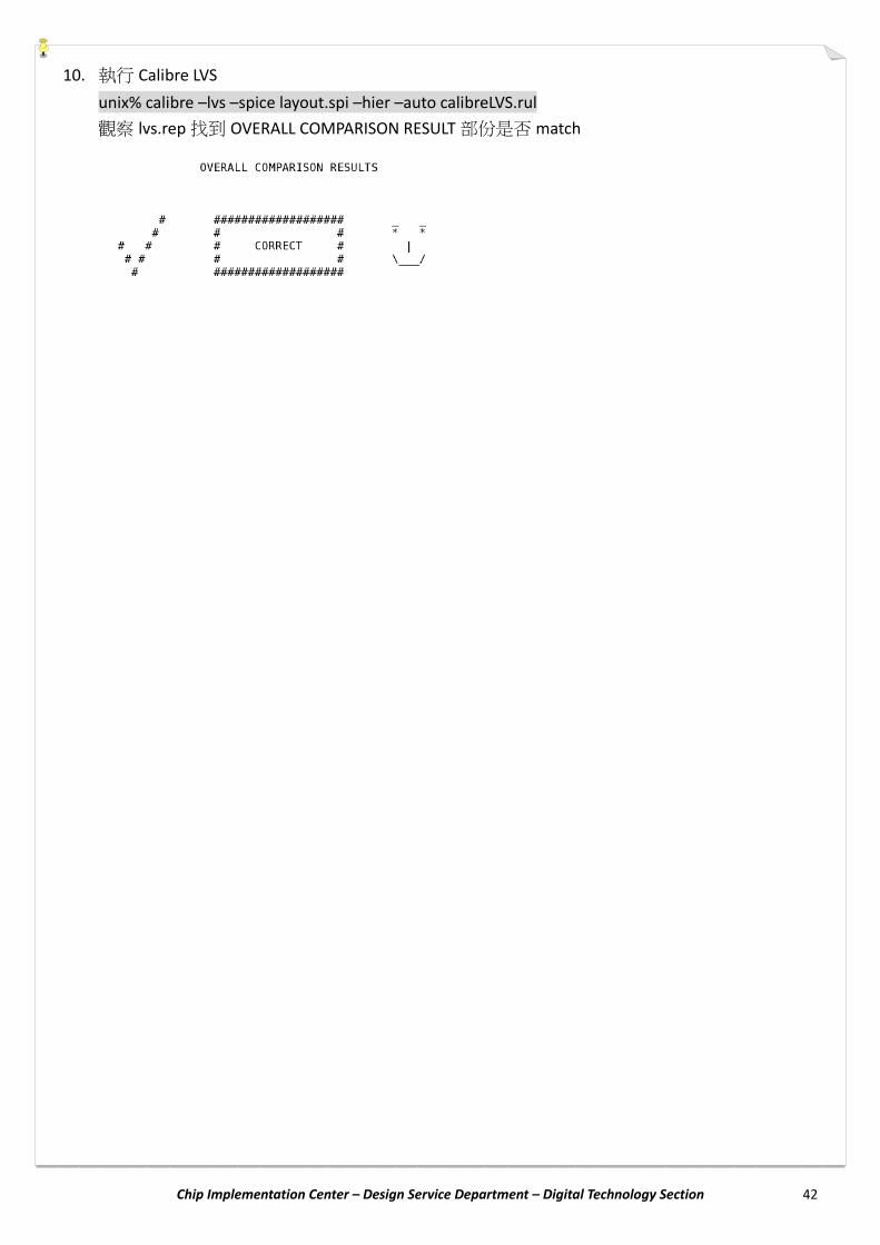
10. 執行 Calibre LVS
unix% calibre –lvs –spice layout.spi –hier –auto calibreLVS.rul
觀察 lvs.rep找到 OVERALL COMPARISON RESULT部份是否 match


![[ASM] Lab2](https://img.pdfslide.us/doc/110x75/588121881a28abb9388b7069/asm-lab2.jpg)