Embed Size (px)
Citation preview

ELEC3342: Digital System Designs
First Semester, 2021–22
Homework3 (r1.1)
Due:
• Part (A) -- 26 Nov, 2021, 11:59pm
• Part (B) -- 26 Nov, 2021, 11:59pm
Instruction: Submit your answers electronically through Moodle.
There are 2 major parts in this homework. Part A includes questions that aim to help you with under-standing the lecture materials. They resemble the kind of questions you will encounter in quizzes andthe final exam. Some of these questions may also ask you to implement and test small designs in VHDL.This part of homework must be completed individually.
Part B of this homework contains a part of the project that you should work in groups of 4. Yoursubmitted work will be graded by an auto tester and therefore you should make sure your submittedfiles conform to the required format.
The following summarize the 2 parts.
Part Type Indv/Grp
A Basic problem set IndividualB Project Group of 4 (same
as HW2)
In all cases, you are encouraged to discuss the homework problems offline or online using Piazza. However,you should not ask for or give out solution directly as that defeat the idea of having homework exercise.Giving out answers or copying answers directly will likely constitute an act of plagiarism, which is aserious offense.

Part A: Problem Set
A.1 Registered Circuit
The following shows a circuit that computes a registered six-input AND function.
A0
A1
A2
A3
A4Y
A5
Figure A.1: A registered 6-input AND gate
Each two-input AND gate has a propagation delay of 100 ps and a contamination delay of 45 ps. Eachflip-flop has a setup time of 57 ps, a hold time of 17 ps, a clock-to-Q maximum delay of 60 ps, and aclock-to-Q minimum delay of 40 ps. Determine the following:
A.1.1 If there is no clock skew, what is the maximum operating frequency of the circuit?
A.1.2 How much clock skew can the circuit tolerate if it must operate at 1.6 GHz?
A.1.3 How much clock skew can the circuit tolerate before it might experience a hold time violation?
A.1.4 Redesign the combinational logic between the registers so they perform the same 6-input ANDfunction but are able to allow the circuit to run faster and tolerate more clock skew.
What is the maximum frequency that your improved circuit can run at? How much clock skew can ittolerate before it might experience a hold time violation?
A.2 Synchronizer MTBF
For your next design, you would like to build a synchronizer that can receive asynchronous inputs withan MTBF of 1 year. You are building the synchronizer using a sampling flip-flop with τ = 100 ps,T0 = 110 ps, and tsetup = 70 ps. The synchronizer receives a new asynchronous input on average 4 timesper second. What is the required probability of failure to satisfy this MTBF? How long would you haveto wait before reading the sampled input signal to give that probability of error? [based on DDCA 3.37 ]
r1.1 Page 2 of 13
ELEC3342: Digital System Designs Homework 3, Part A
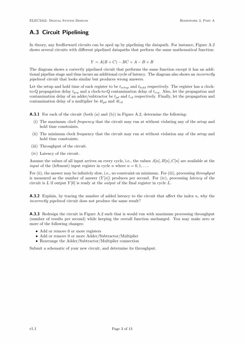
A.3 Circuit Pipelining
In theory, any feedforward circuits can be sped up by pipelining the datapath. For instance, Figure A.2shows several circuits with different pipelined datapaths that perform the same mathematical function:
Y = A(B + C)−BC +A−B ×B
The diagram shows a correctly pipelined circuit that performs the same function except it has an addi-tional pipeline stage and thus incurs an additional cycle of latency. The diagram also shows an incorrectlypipelined circuit that looks similar but produces wrong answers.
Let the setup and hold time of each register to be tsetup and thold respectively. The register has a clock-to-Q propagation delay tpcq and a clock-to-Q contamination delay of tccq. Also, let the propagation andcontamination delay of an adder/subtractor be tpd and tcd respectively. Finally, let the propagation andcontamination delay of a multiplier be 4tpd and 4tcd
A.3.1 For each of the circuit (both (a) and (b)) in Figure A.2, determine the following:
(i) The maximum clock frequency that the circuit may run at without violating any of the setup andhold time constraints.
(ii) The minimum clock frequency that the circuit may run at without violation any of the setup andhold time constraints.
(iii) Throughput of the circuit.
(iv) Latency of the circuit.
Assume the values of all input arrives on every cycle, i.e., the values A[n], B[n], C[n] are available at theinput of the (leftmost) input register in cycle n where n = 0, 1, . . ..
For (ii), the answer may be infinitely slow, i.e., no constraint on minimum. For (iii), processing throughputis measured as the number of answer (Y [n]) produces per second. For (iv), processing latency of thecircuit is L if output Y [0] is ready at the output of the final register in cycle L.
A.3.2 Explain, by tracing the number of added latency to the circuit that affect the index n, why theincorrectly pipelined circuit does not produce the same result?
A.3.3 Redesign the circuit in Figure A.2 such that is would run with maximum processing throughput(number of results per second) while keeping the overall function unchanged. You may make zero ormore of the following changes:
• Add or remove 0 or more registers• Add or remove 0 or more Adder/Subtractor/Multiplier• Rearrange the Adder/Subtractor/Multiplier connection
Submit a schematic of your new circuit, and determine its throughput.
r1.1 Page 3 of 13
ELEC3342: Digital System Designs Homework 3, Part A
A
B
CY
(a) Original Circuit
(b) Pipelined Circuit
(c) Incorrectly Pipelined Circuit
A
B
CY
A
B
CY
Figure A.2: Pipelining a feedforward circuit. (a) original circuit; (b) with 1 pipeline register; (c) incor-rectly pipelined circuit.
r1.1 Page 4 of 13
ELEC3342: Digital System Designs Homework 3, Part A
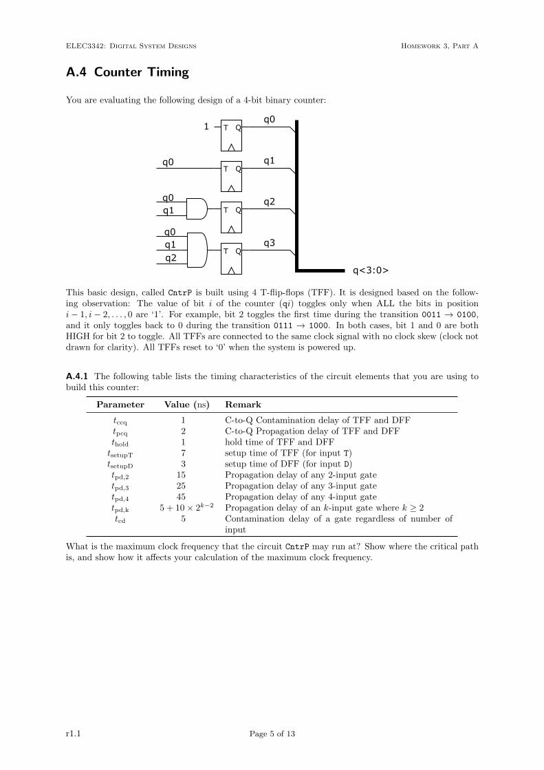
A.4 Counter Timing
You are evaluating the following design of a 4-bit binary counter:
T Q
T Q
T Q
T Q
q01
q0
q0q1
q0q1q2
q1
q2
q3
q<3:0>
This basic design, called CntrP is built using 4 T-flip-flops (TFF). It is designed based on the follow-ing observation: The value of bit i of the counter (qi) toggles only when ALL the bits in positioni− 1, i− 2, . . . , 0 are ‘1’. For example, bit 2 toggles the first time during the transition 0011 → 0100,and it only toggles back to 0 during the transition 0111 → 1000. In both cases, bit 1 and 0 are bothHIGH for bit 2 to toggle. All TFFs are connected to the same clock signal with no clock skew (clock notdrawn for clarity). All TFFs reset to ‘0’ when the system is powered up.
A.4.1 The following table lists the timing characteristics of the circuit elements that you are using tobuild this counter:
Parameter Value (ns) Remark
tccq 1 C-to-Q Contamination delay of TFF and DFFtpcq 2 C-to-Q Propagation delay of TFF and DFFthold 1 hold time of TFF and DFFtsetupT 7 setup time of TFF (for input T)tsetupD 3 setup time of DFF (for input D)tpd,2 15 Propagation delay of any 2-input gatetpd,3 25 Propagation delay of any 3-input gatetpd,4 45 Propagation delay of any 4-input gatetpd,k 5 + 10× 2k−2 Propagation delay of an k-input gate where k ≥ 2tcd 5 Contamination delay of a gate regardless of number of
input
What is the maximum clock frequency that the circuit CntrP may run at? Show where the critical pathis, and show how it affects your calculation of the maximum clock frequency.
r1.1 Page 5 of 13
ELEC3342: Digital System Designs Homework 3, Part A
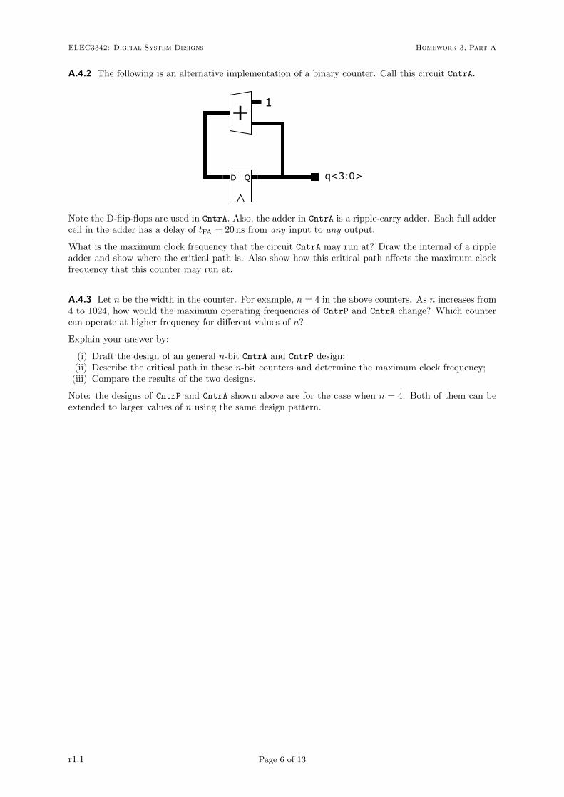
A.4.2 The following is an alternative implementation of a binary counter. Call this circuit CntrA.
D Q q<3:0>
+ 1
Note the D-flip-flops are used in CntrA. Also, the adder in CntrA is a ripple-carry adder. Each full addercell in the adder has a delay of tFA = 20 ns from any input to any output.
What is the maximum clock frequency that the circuit CntrA may run at? Draw the internal of a rippleadder and show where the critical path is. Also show how this critical path affects the maximum clockfrequency that this counter may run at.
A.4.3 Let n be the width in the counter. For example, n = 4 in the above counters. As n increases from4 to 1024, how would the maximum operating frequencies of CntrP and CntrA change? Which countercan operate at higher frequency for different values of n?
Explain your answer by:
(i) Draft the design of an general n-bit CntrA and CntrP design;(ii) Describe the critical path in these n-bit counters and determine the maximum clock frequency;
(iii) Compare the results of the two designs.
Note: the designs of CntrP and CntrA shown above are for the case when n = 4. Both of them can beextended to larger values of n using the same design pattern.
r1.1 Page 6 of 13
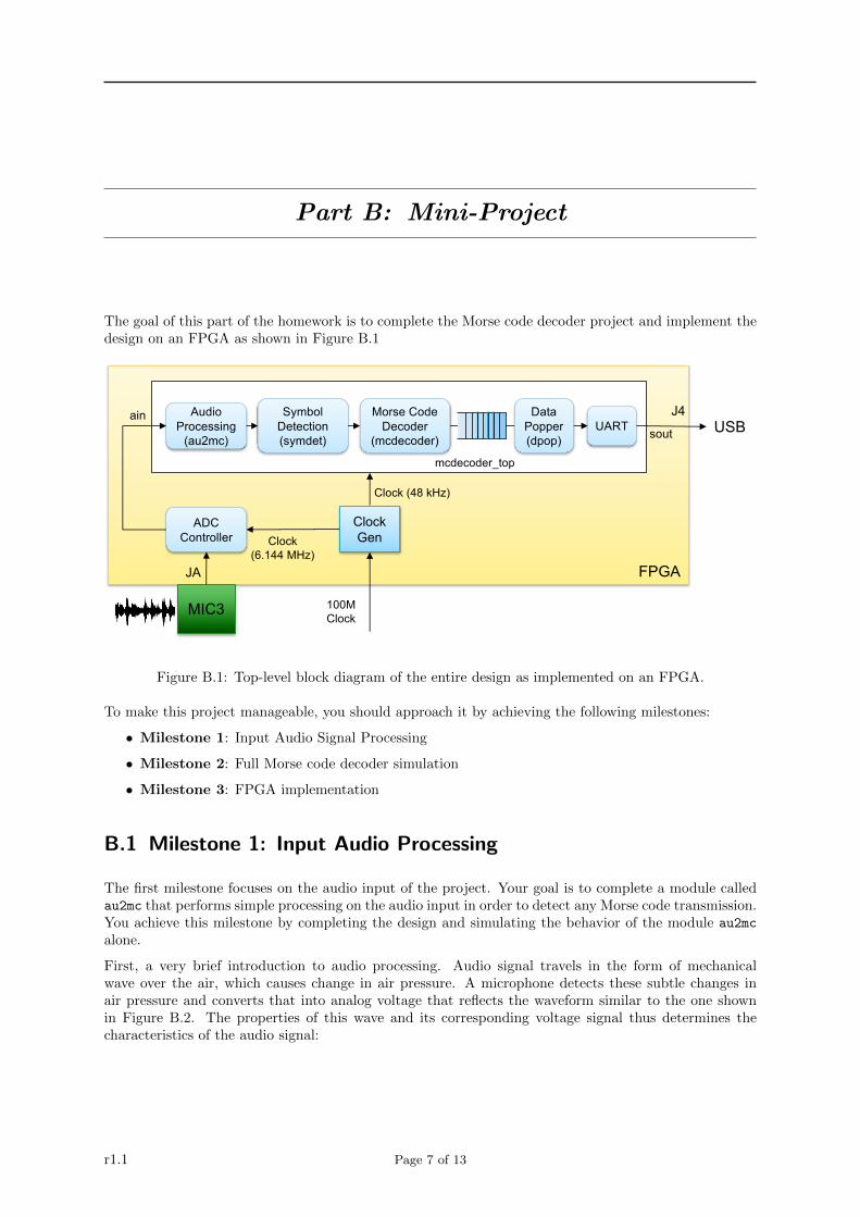
Part B: Mini-Project
The goal of this part of the homework is to complete the Morse code decoder project and implement thedesign on an FPGA as shown in Figure B.1
FPGA
J4
100MClock
Clock (48 kHz)
ADCController Clock
(6.144 MHz)
MIC3
JA
SymbolDetection(symdet)
Morse CodeDecoder
(mcdecoder)UART
AudioProcessing
(au2mc)
Data Popper(dpop)
Clock Gen
USB
mcdecoder_top
ainsout
Figure B.1: Top-level block diagram of the entire design as implemented on an FPGA.
To make this project manageable, you should approach it by achieving the following milestones:
• Milestone 1: Input Audio Signal Processing
• Milestone 2: Full Morse code decoder simulation
• Milestone 3: FPGA implementation
B.1 Milestone 1: Input Audio Processing
The first milestone focuses on the audio input of the project. Your goal is to complete a module calledau2mc that performs simple processing on the audio input in order to detect any Morse code transmission.You achieve this milestone by completing the design and simulating the behavior of the module au2mc
alone.
First, a very brief introduction to audio processing. Audio signal travels in the form of mechanicalwave over the air, which causes change in air pressure. A microphone detects these subtle changes inair pressure and converts that into analog voltage that reflects the waveform similar to the one shownin Figure B.2. The properties of this wave and its corresponding voltage signal thus determines thecharacteristics of the audio signal:
r1.1 Page 7 of 13

ELEC3342: Digital System Designs Homework 3, Part B
Wave Property Audio Property
frequency pitchamplitude volume
shape timbre
For instances, a pure square wave will sound differently from a pure sine wave (timbre). A high frequencysine wave will result in a high pitch, and a loud voice will have wave with high amplitude.
Figure B.2: A typical audio waveform.
In your project, the input Morse code will be transmitted as on-off pulses of audio tones. In the simplestform, these tones are simply pure sine wave of a particular frequency. Figure B.3 shows an ideal inputMorse code waveform to your circuit.
B.1.1 Data Transmission & Encoding In this project, you will use an analog-to-digital convertor (ADC)to convert the analog voltage produced by the microphone into digital signals (numbers) for processingon the FPGA. The external ADC is included in a small board called MIC3. Details can be found fromthe course website.
The sampled data from the ADC are encoded as simple binary numbers from 0000 0000 0000 to1111 1111 1111. A study of the MIC3 schematics show that the code 0000 0000 0000 represents themost negative air pressure while 1111 1111 1111 represents the most positive pressure. In other word,when there is no sound (0 air pressure, the reading is around 0111 1111 1111. It is just an estimate asit depends on actual calibration of the circuit.
Figure B.3: Sample input waveform with Morse code transmitted. The input will be a tone around 50 Hzsine wave. The tone is pulsed as Morse code.
r1.1 Page 8 of 13
ELEC3342: Digital System Designs Homework 3, Part B
In other words, the data values you are receiving from the ADC are not represented by the usual 2scomplement representation. You will need to subtract 1000 0000 0000 from the input to obtain the 2scomplement representation of the data values.
B.1.2 Detecting Sound Source There are many ways you can process the audio samples to determineif there is a valid sound input. Here, a very simple thresholding scheme is shown. You are free to imagineyour own scheme, or to apply sophisticated audio signal processing schemes here if you wish.
In this simple scheme, the central idea is to notice that in the ideal Morse code waveform (similar tothat shown in Figure B.3), all your circuit needs to perform is to detect if there is any sound. If thereis NO sound (silence), then it should output ‘0’. If there is ANY sound, it should output ‘1’.
Since the amplitude of a wave represents the level of sound, this simple scheme essentially performs amoving average of the input voltage amplitude over a small sampling window. If the average is abovecertain threshold, it regards there is audio input. If the average amplitude is below the threshold, itshould be treated as silence.
B.1.3 Average Amplitude Let a[n] be the sampled value (amplitude) at time step n. Then the movingaverage of the amplitude at step n over a window size of W is defined as:
a =1
W
W−1∑i=0
|a[n− i]| (B.1)
For your project, set W to a suitable value that is power of 2 and you will then be able to compute (B.1)with simple add and shift operations without performing divisions.
Note that there is an absolute operation in (B.1). You may consider either implementing a true absolutefunction (which is not difficult), or you may additionally use an approximation:
|a| ≈ max(0, a) (B.2)
You should explore different values of W or different ways to compute moving average to obtain betterresults.
B.1.4 Audio Processing Output The goal for the audio processing module au2mc is to produce thenecessary dbin signal, which is the input to the symdet module. As mentioned, you should processaudio signals with the clk 48k clock, which results in a 1 or 0 at 48 kHz. As you will be sampling at48 kHz, it means you simply need to determine the output every cycle, possibly based on the result ofthe moving average computation and a threshold that you set internally.
B.1.5 Testing & submission A testbench program tb au2mc has been provided to you. Note: althoughthe testbench program is written in VHDL, just as any other testbench programs, it is NOT part of thefinal hardware design.
In this case, the code inside tb au2mc reads an audio file from your computer and send the audio sampledata to your hardware module au2mc for simulation. You can check the output of au2mc in the simulatorto make sure it produces the expected output, i.e., sequence of 1 and 0 representing Morse code.
3 audio files are provided to you for testing. You can also record your own if you wish. Ask on Piazzafor the procedures to create these audio files1.
Submit the simulation waveform output in your report for this Milestone.
1The process is basically to convert standard WAV files with integer encoding using standard audio processing tools.
r1.1 Page 9 of 13
ELEC3342: Digital System Designs Homework 3, Part B
B.2 Milestone 2: Full Morse code decoder simulation
The target of this milestone is to complete the full Morse code decoder and to simulate the function ofthe full system. Specifically, you will implement and simulate the function of the block mcdecoder top
shown in Figure B.1.
Except for the clk and clr signals, mcdecoder top simply takes audio samples as input (ain) and pro-duces a serial signal (sout) for UART transmission. To complete this milestone, you need to demonstratethrough simulation, that your mcdecoder top design can take in the audio sample from a testbench (sameas the ones in Milestone 1), decode the signal to a valid ASCII character, and produce the necessaryserial output from the UART.
Since most of the blocks needed to implement mcdecoder top have already been designed in HW1, HW2and Milestone 1, you only need the following to achieve Milestone 2:
• Create a new VHDL module mcdecoder top that instantiate all the blocks;
• Modify symdet from HW2 such that it works with input with a large base unit u;
• Design a small data popper (dpop to connect the output of the FIFO to the input of UART.
B.2.1 Top level module To design and simulate the top-level module mcdecoder top, you need to createa new project that includes all the modules that you will needed. A few notes about this integration:
• You need to create your own top level VHDL file, mcdecoder top, that combines all the modules.This top level VHDL entity has the same input as au2mc (i.e., audio sample, clock and clear), andproduces output the same as the UART (a single bit).
• The modules symdet and mcdecoder are from Homework 1 and 2. You need to include the designfrom your own group from homework 1 and 2. You may, and you should, improve the functionalityof these modules if they were not fully functional when you turned in homework 1 and 2. You mayuse the posted sample answer as a starting point to help improve your original design.
• You can assume your entire system operates on a 48 kHz clock, which will be passed to your systemthrough the clock port (clk).
To simulate the behavior of the system, you need to build a new testbench file tb mcdecoder top, whichis mostly the same as tb au2mc, except you need to make sure you can reset (clr) the system correctlyin the simulation. See below section about FIFO.
B.2.2 Modify Symbol Detector In homework 2, you had the choice to implement symdet at differentlevels. When working with real-world input, you need a symdet module at L3 in theory. For this project,the audio test input will always have a fixed value of u. As a result, you will need only a L2 symdet witha large but almost fixed value of u. The exact value of u depends on your au2mc, but should be around3000. That is, a dot will be about 3000 cycles and a dash is about 9000 cycles. The value of u will notbe exact even when the input audio is produced by a computer due to factors such as how the audio isrecorded, what is the phase of the audio wave, how your au2mc is implemented etc. For this homework,you will need to modify your symdet from homework to work with this range of u values.
B.2.3 Data popper In mcdecoder top, there is a FIFO between the output of mcdecoder and theUART. If you use a standard or built-in FIFO (like in HW2), the data that you have pushed into theFIFO will simply reside inside the FIFO until they are externally popped. At the same time, the UARTwould passively wait for data to be transmitted.
As a result, you need to implement a simple circuit that connect the two. In this project, we call it a“data popper” (dpop). The design of dpop is quite straightforward:
r1.1 Page 10 of 13
ELEC3342: Digital System Designs Homework 3, Part B
dpop should monitor the control signals (e.g. empty from the FIFO and the UART (e.g. ready), andwhen both of them are asserted (FIFO is not empty and UART is ready, then it should pop a data fromthe FIFO and send the data to the UART.
Implement dpop and use it in mcdecoder top. To help with your debugging effort, you probably wantto design and test it separately before using it in the over system.
B.2.4 FIFO If you use the built-in FIFO from the Vivado tools, then you must do the following in orderto simulate the operation of the FIFO:
• Make sure you have the following library included (uncomment them if you produced your top levelVHD file from Vivado) in your top level module mcdecoder top:
library UNISIM;
use UNISIM.VComponents.all;
• Instantiate the FIFO in your design. HINT: You can copy-and-paste the port definition from theproduced VHDL (fifo generator 0) for your convenience.
• IMPORTANT: Make sure you RESET the system in the beginning of your simulation (by settingyour clr signal high for a short time before turning it back to ‘0’. The Xilinx produced FIFOMUST be initially reset at least once for it to behave correctly in simulation.
If you designed your own FIFO, then you may ignore the part about the use of UNISIM library.
B.2.5 Simulating Whole System With all the pieces, you should now be able to simulate the functionof the entire system in Vivado. Remember to change the simulation duration to a larger value so youcan simulate the operation of the system for the complete audio input.
B.2.6 Milestone Submission Show the simulation waveform using the 3 provided audio files as inputs.Make sure you highlight (i) the output from the module mcdecoder with correctly decoded ASCIIcharacters, and (ii) the serial output from the UART when the corresponding character is sent to thecomputer. Hint: If you fail to implement the whole system, try to demonstrate at least part of thesystems. For example, if you fail to implement an improved symdet that works with large values ofu, then you may consider simulating a design without au2mc and use the L0 testbench from HW2 tosimulate the rest of the design.
r1.1 Page 11 of 13

ELEC3342: Digital System Designs Homework 3, Part B
B.3 Milestone 3: Implementation on FPGA
In this part of the project, your task is to implement your design from homework 2 on the actual FPGAboard. For your reference, the board you will be using is the Digilent Basys 3 board. The main FPGA onyour board is a Xilinx Artix-7 FPGA (XC7A35T- 1CPG236C). For details of the board, please refer tothe Basys 3 FPGA Board Reference Manual. (Note: on Digilent website the link is labeled as Datasheet.)
A sample project, called au2mcdecoder is provided to you with all of the necessary additional circuitsand configurations correctly setup to help you implement the design on the FPGA board.
B.3.1 Clock An important part of a real project, as oppose to a simulation project, is that you need torun with an actual clock signal. On the Basys 3 board, a 100 MHz clock source is available and you willuse that as the main clock course in your design.
In your design, you will need 2 clock signals to drive different parts of the circuits:
• clk 6144: A 6.144 MHz clock used in the audio ADC controller;
• clk 48k: A 48 kHz clock used for the main design.
For those of you who are curious, the above clock frequencies are chosen specifically for ease-of-implementationin your design: 48 kHz is a common audio processing sampling rate, and is also 5 times higher than the9600 baud rate needed for UART communication. 6.144 MHz is 128 times higher than the main clockfrequency, and can be precisely produced from the 100 MHz clock source with the FPGA’s on-boardmulti-mode clock management (MMCM) circuit.
The circuits required to produce these clock signals are already provided to you. Feel free to explore howthey work but DO NOT modify any of these circuits.
B.3.2 Audio Input On the actual FPGA board, an external microphone is used to listen to your realworld audio input. The audio module you will used is the Digilent Pmod MIC3 modules, which containsa Knowles Acoustics SPA2410LR5H-B microphone and a Texas Instruments ADCS7476 analog-to-digitalconverter.
A basic controller (adccntlr is provided to you. It’s job is to communicate with the ADC to commandthe ADC to produce an audio sample. For this project, the controller sample the audio signal at a fixedrate of 48 kHz with 12− bit accuracy. In other words, it produces a 12-bit sample every 1/48000 seconds.These audio data sample will then become the digital audio samples that can be processed in later steps.Recall that your system is also running at 48 kHz by design. Therefore, it means the module is produceexactly 1 sample every cycle. It is designed specifically this way to make your design simple, and tomake it matches the expected behavior from Milestone.
B.3.3 Implement Design Once you have all the files set up, click the “Run Synthesis” button to startthe synthesis process. If your synthesis runs correctly (check for Error and Warning messages), youshould also run the “Generate Bitstream” step of the Vivado tool flow.
B.3.4 Configure FPGA To test your design on the Basys 3 FPGA board, do the following:
• Connect your Basys 3 board to your computer with a micro-USB cable. Connect your cable toconnector J4 (labeled as PROG on the board).
• Turn on the FPGA board. By default you will see numbers showing up on the 7-segment displayand increases every second. It is the default designs shipped from the factory.
• To configure the FPGA, select “Open Hardware Manager” from Vivado. Your FPGA boardshould show up under the Hardware pane.
r1.1 Page 12 of 13
ELEC3342: Digital System Designs Homework 3, Part B
• Right click on the FPGA showed up (Artix-7) and select “Program Device. . .”. Select thebitstream that you have just created (usually with the same name as your project with a .bit
extension.)
B.3.5 Serial Terminal In order to receive data from your Basys 3 board, you need to run a serialterminal program on your host computer. Make sure you set up your serial terminal with 9600 baudrateand 8-N-1 configuration. Refer to homework 2 handout for more details.
The default configuration for the Basys 3 board will send a text string to the host computer when it firststarts up through its UART. You should use this as a test of your serial connection before you test yourown design.
If you set up is correct, when the Basys 3 starts up you should see a text string show on your computerscreen.
Congratulation! If you can see the correctly decoded message on your computer screen, your Morse codedecoder’s decoding logic is completed!
B.4 Submission
For Part B of this homework, turn in, as a group, a report describing your design. Include a top-levelblock diagram of your audio processing module. Include all the items mentioned from each Milestoneabove. Specifically, explain (i) the algorithm that you have implemented to perform audio detection, (ii)any modification of symdet from hw2 (iii) your data popper at the output of the FIFO.
Then during project demo, be prepared to show a working design. Before you attend the interview,setup the board and load the correct bitstream to the board for demo.
r1.1 Page 13 of 13


![Homework 3]](https://img.pdfslide.us/doc/110x75/55b6ace7bb61eba5488b459c/homework-3-55bd3bece5fe2.jpg)