Embed Size (px)
Citation preview

Highly Sensitive Light-induced Memory Effect withAmorphous Se-SnO2 Heterojunction
Masahiro Okuda, Tatsuhiko Matsushita, Teiichi Yamagami, and Koichi Yamamoto
The light-induced memory effect in amorphous selenium films is studied by fabricating them into a sortof heterojunction (Se-SnO2) so as to be able to apply the bias voltage together with the laser beam irra-diation for memory. Under the reverse bias voltage, a region of high electric field is formed in the seleni-um film near the junction. Remarkable enhancement in the photo-induced image spot is achieved if anappropriate bias voltage is applied simultaneously, indicating the sensitization of the memory effect dueto the photocurrent induced by the high electric field in the selenium film.
1. Introduction
Photo-induced effects that occur in thin films ofamorphous materials under the illumination of thelaser light of appropriate intensity and duration havebeen studied for a number of chalcogen-based sys-tems. For the systems Ge-Te-Sb-S,' Ge-As-Te,2,3and Ge-As-Se,4 the effect has been interpreted asdue to a structural change of the irradiated areafrom the amorphous state to a crystalline one. Inother chalcogenide systems based on long chainpolymeric glasses, Ovshinsky and Klose5 and Fein-leib et al.6 have found a similar optical effect, whichshould, however, be ascribed to a mechanism differ-ent from that based on the amorphous-crystallinetransformation.
Recently, Maruyama et al. 7 have shown that a re-markable sensitization in the light-induced memoryeffect can be achieved by the simultaneous applica-tion of the pulses of laser radiation and bias voltageto the samples consisting of four layers of SnO2,CdS, amorphous chalcogenide, and Au successivelydeposited onto the glass substrates. Further, anelectrical enhancement for hologram memory hasbeen found on the amorphous semiconductor belong-ing to Ge-As-Te.8
In this report, the light-induced effect is examinedwith amorphous selenium films fabricated into aform of diode by successive deposition of Se and Auonto the SnO2-coated class substrates. The junctionis formed at the interface between the p-type Se filmand the degenerated n-type SnO2 layer, and imagingby a focused laser beam is thus performed with orwithout applying the bias voltage across the junc-
The authors are with the College of Engineering, University ofOsaka Prefecture, Mozu, Sakai, Osaka, Japan 591.
Received 27 August 1973.
tion. When the specimen is subjected to an appro-priate bias voltage, the diameter of the image spotbecomes appreciably larger. 9 "10 The observed re-sults of such a sensitization will be described with adiscussion on the possible mechanism for it.
11. Experimental Procedures and ResultsA schematic construction of the specimens is
shown in Fig. 1. The Se film, 1-10,4m thick, is de-posited on the SnO2 layer of NESA glass substrate,being followed by another deposition of an Au layer1000-2000 A thick and 1 2 mm2 in size, to yieldthe electrode of ohmic contact to the Se film. Forthe image formation, the pulsed light irradiated at6328 A from a He-Ne laser is focused by an objectivelens of a microscope onto the Se film through theglass substrate. The peak power of the focusedbeam can be changed from 1 mW to 10 mW at theimage spot about 2 ,um in diameter and the pulseduration of light is adjustable in the range from 1 to1000 msec.
Figure 2 shows image spots formed in a specimen,4.6 m thick, after irradiation at light power of6.6 mW and duration of 1 msec without applyingany bias voltage to the junction. The experimentalresults obtained, without applied bias voltage, undervarious radiation intensities and durations are sum-marized in Fig. 3. For the upper right region of thefigure, the radiation energy is too high to avoid evap-oration of the film at the illuminated spot, while thelower left region shows a shortage of power. Theshaded area corresponds to the successful write-inconditions. Moreover, the spot diameter obtained ata constant laser energy depends on the thickness ofSe film, as shown by an example in Fig. 4 (laserpower 6.6 mW, pulse duration 1 msec). From theseresults, it is seen that the spot diameter becomes amaximum for the Se films 3-6 im in thickness, and
April 1974 / Vol. 13, No. 4 / APPLIED OPTICS 799

Au Se
-G~las l~l~l~lfl11 11 I.: ., ,,,,,,,,,,,,,,,,,,-.-.
Glass SnO2substrate Focused beam
_r'_-g1.C srcinfsmlFig. 1. Construction of sample.
0 0 0
thus the optimum film thickness should be takeninto account to obtain a high sensitivity for laserwriting.
The current-voltage characteristics. of the samplewith Se films, 1.0 m, 4.6 Am, and 10 Am in thick-ness, respectively, are shown in Fig. 5. All sampleshave a good rectification property and the ratio ofrectification is about 10-30.
For the writing operation on the sample with itsAu electrode biased positively or negatively, namely,with the heterojunction forwardly biased or reverselybiased, it is recognized that the diameter of spots in-creases appreciably in comparison with that ob-tained without the applied bias voltage.
An example for such an enhancement effect isshown in Fig. 6, where the thickness of Se film is 10Am. Here, it is worth noting that the diameter of
l(pA) 1(pA)
10
Fig. 2. Image spots obtained by laser irradiation with no biasvoltage (radiation time 1 msec and radiation power 6.6 mW).
0.1
Radiation
Fig. 3. Conditions for laser writing foundbias voltage.
0_L_10° 10IFilm thickness(um)
io time(sec)
without applying any
1urm 10
10 100 500 V(V) 10Forward
1umI10 PM
100 500 V(V)Reverse
Fig. 5. Current-voltage characteristics of samples (selenium filmthickness 1.0 um, 4.6 am, and 10 Mm; area of electrode 1 x 2
mm2
).
*-500V
+400
0 ~4+300
) X:f0O
10Z
Fig. 4. Relation between the spot diameter nd the film thick-ness (radiation power 6.6 mW and radiation time 1 msec).
Fig. 6. Image spots obtained under various bias voltages (radia-tion time 1 msec radiation power 6.6 mW, and selenium film
thickness 10 um).
800 APPLIED OPTICS / Vol. 13, No. 4 / April 1974
6
E 5
3r 400.
(A 3.
2
0
8
E
U)
U1)ECU2ii
0R
6
4
2
n-1
10
Spot diameter( um)p-i
4.6,um
_L ,4 1
-16 V-2
damage
)um
-8 -4
8
6 10,um 4.6,um 1pm
4
-2
0 4 8 12 16 x 10E( V/cm)
Fig. 7. Relation between the spot diameter and the intensity ofthe applied electric field.
A-
10 -
81
6-
4-
2
-600 -400 -200 C
8
Au (eI
200 400 600V(V)
Fig. 8. Sensitization for the memory effect in selenium films ofvarious thicknesses, A is the sensitizing region and B the burn-
out region.
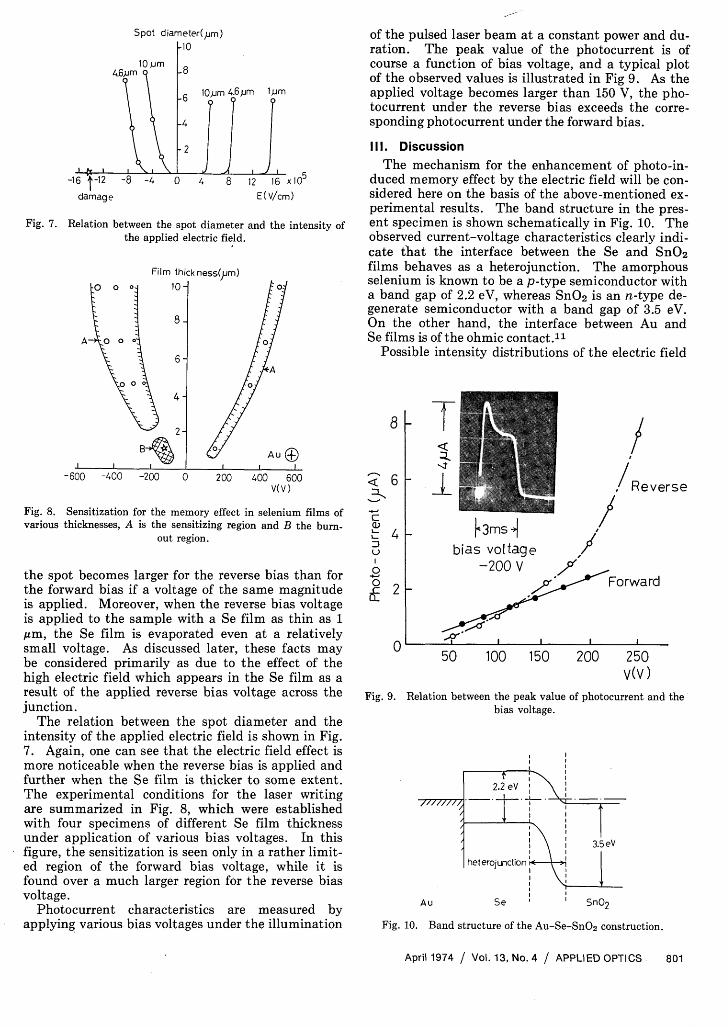
the spot becomes larger for the reverse bias than forthe forward bias if a voltage of the same magnitudeis applied. Moreover, when the reverse bias voltageis applied to the sample with a Se film as thin as 1Am, the Se film is evaporated even at a relativelysmall voltage. As discussed later, these facts maybe considered primarily as due to the effect of thehigh electric field which appears in the Se film as aresult of the applied reverse bias voltage across thejunction.
The relation between the spot diameter and theintensity of the applied electric field is shown in Fig.7. Again, one can see that the electric field effect ismore noticeable when the reverse bias is applied andfurther when the Se film is thicker to some extent.The experimental conditions for the laser writingare summarized in Fig. 8, which were establishedwith four specimens of different Se film thicknessunder application of various bias voltages. In thisfigure, the sensitization is seen only in a rather limit-ed region of the forward bias voltage, while it isfound over a much larger region for the reverse biasvoltage.
Photocurrent characteristics are measured byapplying various bias voltages under the illumination
of the pulsed laser beam at a constant power and du-ration. The peak value of the photocurrent is ofcourse a function of bias voltage, and a typical plotof the observed values is illustrated in Fig 9. As theapplied voltage becomes larger than 150 V, the pho-tocurrent under the reverse bias exceeds the corre-sponding photocurrent under the forward bias.
111. Discussion
The mechanism for the enhancement of photo-in-duced memory effect by the electric field will be con-sidered here on the basis of the above-mentioned ex-perimental results. The band structure in the pres-ent specimen is shown schematically in Fig. 10. Theobserved current-voltage characteristics clearly indi-cate that the interface between the Se and SnO2films behaves as a heterojunction. The amorphousselenium is known to be a p-type semiconductor witha band gap of 2.2 eV, whereas SnO2 is an n-type de-generate semiconductor with a band gap of 3.5 eV.On the other hand, the interface between Au andSe films is of the ohmic contact.'
Possible intensity distributions of the electric field
50 100 150 200 250V(V)
Fig. 9. Relation between the peak value of photocurrent and thebias voltage.
Au Se
Fig. 10. Band structure of the Au-Se-SnO 2 construction.
=I
C:PL.
U
0
6
4
2
0
April 1974 / Vol. 13, No. 4 / APPLIED OPTICS 801
: --
B_I I %
I I
I71 I
Sno2

Reverse
Au ESeSn
(a) ( b)
Fig. 11. Intensity distributions of the electric field in the seleni-um film. (a) Selenium film thickness 4.6 pm. (b) Selenium film
thickness 1.0 im.
generated in the Se films are depicted schematicallyin Fig. 11(a) for a thick Se film (4.6 Am) and in Fig.11(b) for a thin Se film (1.0 Mim). In Fig. 11(a), thedistribution is rather uniform for the forward bias,while for the reverse bias the region of high field in-tensity localized near the heterojunction should beformed corresponding to the presence of the deple-tion layer. On the other hand, in Fig. 11(b), the Sefilm is so thin that the width of the depletion layerbecomes comparable to the Se film thickness whenthe reverse bias is applied.
If the sample is subjected to the illumination of alaser pulse under an applied forward bias, electronsand holes generated in the Se film will travel, re-spectively, toward the Au and SnO2 electrodes.However, the drift velocity of the carriers cannot bevery high since the field intensity is rather uniformin the Se film. Therefore, the electric field effect forthe light-induced memory is not so significant in thiscase.
In the reverse bias, in contrast, the drift velocity ofthe carriers must be very high since the carriersshould be accelerated by the high field intensity inthe Se film.
Such a point of view is actually supported by theresults obtained from the photocurrent measure-ments as shown in Fig. 9. In fact, for the specimenin Fig. 9, the photocurrent at the reverse bias voltageof 250 V amounts. to 7.9 MA in spite of the fact thatthe static reverse current at the same bias voltage isonly 0.1 MiA (Fig. 5).
The observed sensitization in the light-inducedmemory effect under the reverse bias voltage is thusconsidered to originate from this photocurrent pro-duced by the high electric field in the depletionlayer. Therefore, a highly sensitive amorphous pho-toconductor is desirable for the construction of amemory device described here.
Finally, it should be added that the photo-inducedimage spot in the present specimen can be erased atan elevated temperature by flowing the current
through the SnO2 film. The erasing current is about60 mA in the case of a SnO2 film, 2 mm in widthand 600 A thick.
IV. Summary
The light-induced memory effect in amorphous se-lenium film is studied by fabricating them into a sortof heterojunction so as to be able to apply the biasvoltage together with the laser beam irradiation formemory. Under the reverse bias condition, the re-gion of high electric field is formed in the seleniumfilms near the junction. Remarkable enhancementin the photo-induced image spot is achieved if an ap-propriate bias voltage is applied simultaneously.The mechanism for the enhancement of photo-in-duced memory effect by the electric field is consid-ered on the bases of the current-voltage characteris-tics and photocurrent-voltage characteristics. Thephotocurrent induced by the high electric field in thedepletion layer is considered as the most responsiblefor the enhancement of the memory effect. Thelight-induced image spot can be erased thermally byflowing the electric current through the SnO2 film.
The authors are happy to thank S. Saito for sever-al discussions.
References1. J. Feinleib, J. de Neufville, S. C. Moss, and S. R. Ovshinsky,
Appl. Phys. Lett. 18, 254 (1971).2. S. Asai and E. Maruyama, in Proceedings of the 2nd Confer-
ence on Solid State Devices (Jap. Soc. Appl. Phys., Tokyo,1970), p. 172.
3. A. Hamada, T. Kurosu, M. Saito, and M. Kikuchi, Appl.Phys. Lett. 20, 9 (1972).
4. T. Igo and Y. Toyoshima, in Proceedings of the 3rd Confer-ence on Solid State Devices (Jap. Soc. Appl. Phys., Tokyo,1971), p. 61.
5. S. R. Ovshinsky and P. H. Klose, J. Non-Cryst. Solids, 8-10,892 (1972).
6. J. Feinleib, S. Iwasa, S. C. Moss, J. P. de Neufville, and S. R.Ovshinsky, J. Non-Cryst. Solids, 8-10, 909 (1972).
7. M. Terao, H. Yamamoto, and E. Maruyama, Proceedings ofthe 4th Conference on Solid State Devices (Jap. Soc. Appl.Phys., Tokyo, 1972), p. 233.
8. K. Sakurai, T. Morikawa, and T. Nakajima, Lecture 950 inAnnual Meeting of Electronics and Communication of Japan(April 1973).
9. M. Okuda, T. Matsushita, T. Yamagami, and K. Yamamoto,Jap. J. Appl. Phys. 12, 481 (1973).
10. M. Okuda, T. Matsushita, T. Yamagami, and K. Yamamoto,Jap. J. Appl. Phys. 12, 769 (1973).
11. J. L. Hartke, Phys. Rev. 125, 1177 (1962).
802 APPLIED OPTICS / Vol. 13, No. 4 / April 1974