Embed Size (px)
Citation preview

Oxide Aperture Heterojunction Bipolar
Transistors
James G. Champlain
Ph.D. DefenseUniversity of California, Santa Barbara
February 22, 2002
PhDDefenseAcknowledgements
Advisor Umesh MishraCommittee Art Gossard, Evelyn Hu, and Jim SpeckMishra Group (old and new)
Ale, Ariel, Can, Dan, Dario, DJ, Gia, Haijiang, Huili, Ilan, Jae, Jason, Jeff, Lee,Likun, Mary, Naiqain, Nguyen, Peter, Prashant, Primit, Rama, Rob C., Rob U.,Sten, Tim, Yifeng, and Yingda
Yee Kwang for all the discussions on HBTs and his excellent simulationsYork Group
Amit, Angelos, Baki, Bruce, Chris, Hongtao, Jim, Joe, Justine, Nadia, Nick, Paolo,Pengcheng, Pete, Troy, and Vicki
MBEJohn English
System B Eric, Prashant, Richard, SheilaFriends
Todd, Dave, and JohnNick, Omer, Cathy, Fay, Rex, Fereshteh, Neil, Heather, and Stefanie
Peter, Lee, and Rama
Eric, Prashant, Richard, Sheila, Borys, Can, Dave, and Max

PhDDefenseOverview
Introduction
Oxide Aperture HBTs
Growth as related to bipolar transistors Growth of GaAs0.49Sb0.51, AlAs0.56Sb0.44, and AlxGa1-xAsySb1-y
n-type doping of arsenide-antimonides
Current density: area versus perimeter Aperture placement Diode Selection Rules
Generation Ø Generation I Generation II RF results
Transistor Design and Growth
Oxide Aperture Diodes
Conclusions and Future Work

PhDDefenseIntroduction
device circuit system
device circuit system
complexity
device circuit system
requiredoperatingfrequency
complexity
The ever-growing demand in communication and radar technology for increased bit-rates and frequency resolution requires systems capable of providing increased bandwidth and clock rates
Requires increased bandwidth from the devices, which are the building block of the system
As complexity increases, the max operating frequency decreases
A given system frequency, a higher device operating frequency is required
Given that these systems are built from circuits, which in turn are built from basic devices and passive elements
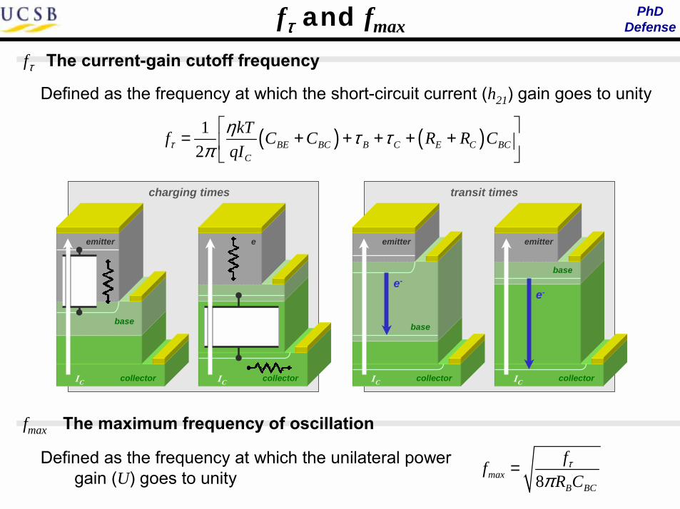
PhDDefensefττττ and fmax
fτ The current-gain cutoff frequency
fmax The maximum frequency of oscillation
Defined as the frequency at which the short-circuit current (h21) gain goes to unity
Defined as the frequency at which the unilateral power gain (U) goes to unity
( ) ( )12 BE BC B C E C BC
C
kTf C C R R CqIτη τ τ
π
= + + + + +
transit times
IC
emitter
collector
base
e-
IC
emitter
collector
base
e-
base
collector
emitter
IC IC
e
collector
charging times
8maxB BC
ffR C
τ
π=
PhDDefense
selective regrowth techniques
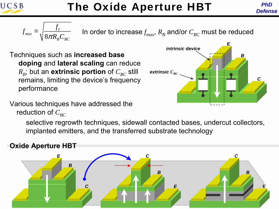
The Oxide Aperture HBT
8maxB BC
ffR C
τ
π= In order to increase fmax, RB and/or CBC must be reduced
Techniques such as increased base doping and lateral scaling can reduce RB; but an extrinsic portion of CBC still remains, limiting the devices frequency performance
intrinsic deviceE
B
Cextrinsic CBC
Various techniques have addressed the reduction of CBC
E
B
C
B
E
C
E
C
B
Oxide Aperture HBT
selective regrowth techniques, sidewall contacted basesselective regrowth techniques, sidewall contacted bases, undercut collectorsselective regrowth techniques, sidewall contacted bases, undercut collectors, implanted emittersselective regrowth techniques, sidewall contacted bases, undercut collectors, implanted emitters, and the transferred substrate technology

PhDDefenseOverview
Introduction
Oxide Aperture HBTs
Growth as related to bipolar transistors Growth of GaAs0.49Sb0.51, AlAs0.56Sb0.44, and AlxGa1-xAsySb1-y
n-type doping of arsenide-antimonides
Current density: area versus perimeter Aperture placement Diode Selection Rules
Generation Ø Generation I Generation II RF results
Transistor Design and Growth
Oxide Aperture Diodes
Conclusions and Future Work
Introduction
Oxide Aperture HBTs
Current density: area versus perimeter Aperture placement Diode Selection Rules
Generation Ø Generation I Generation II RF results
Oxide Aperture Diodes
Conclusions and Future Work

PhDDefenseTransistor Design: Materials
The majority of high-speed HBTs produced today have been InP emitter-up transistors
n+ InGaAs emitter contact
n+ AlInAs emitter
n grade from InGaAsto AlInAs
p+ InGaAs base
n- InGaAs collector
n+ InGaAs sub-collector
AlInAs does not readily oxidize and cannot be easily used to form an oxide apertureRox,AlInAs = 2.4 µm/hr @ 520 °C
substrate
emitter
emitt
er
base
base
collector
colle
ctor
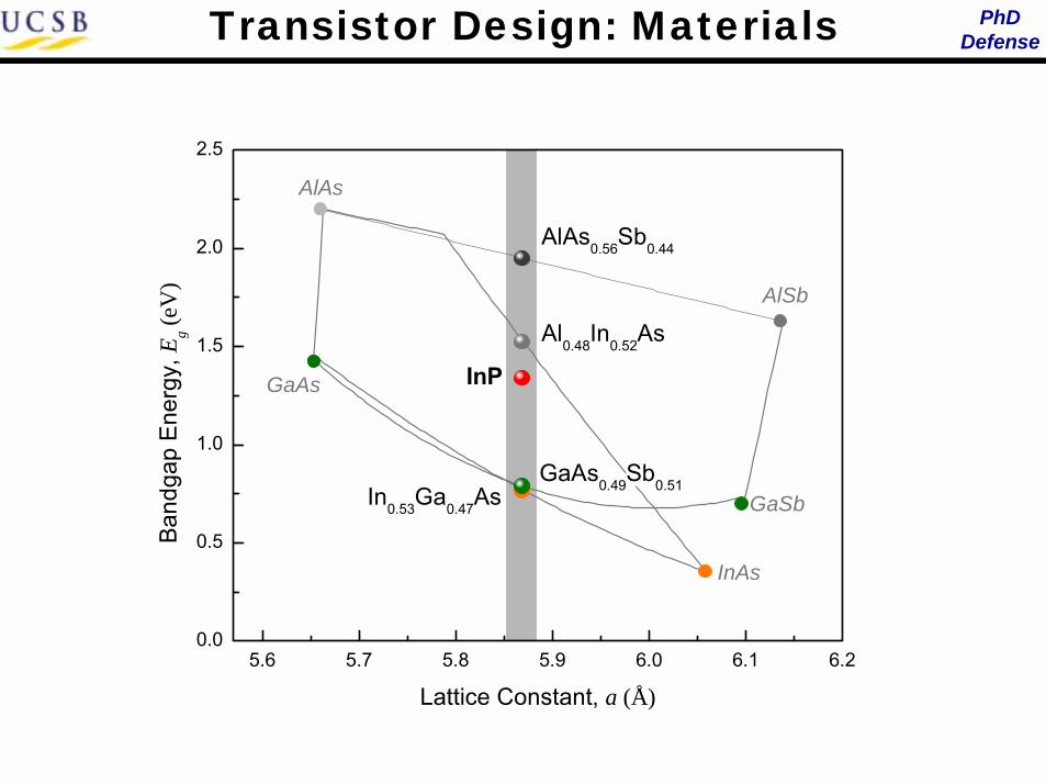
PhDDefenseTransistor Design: Materials
5.6 5.7 5.8 5.9 6.0 6.1 6.20.0
0.5
1.0
1.5
2.0
2.5
Band
gap
Ener
gy, E
g (eV
)
Lattice Constant, a (Å)5.6 5.7 5.8 5.9 6.0 6.1 6.2
0.0
0.5
1.0
1.5
2.0
2.5
InAs
AlAs
GaAs
Band
gap
Ener
gy, E
g (eV
)
Lattice Constant, a (Å)5.6 5.7 5.8 5.9 6.0 6.1 6.2
0.0
0.5
1.0
1.5
2.0
2.5
InP
InAs
AlAs
GaAs
Band
gap
Ener
gy, E
g (eV
)
Lattice Constant, a (Å)5.6 5.7 5.8 5.9 6.0 6.1 6.2
0.0
0.5
1.0
1.5
2.0
2.5
InP
InAs
AlAs
GaAs
Band
gap
Ener
gy, E
g (eV
)
Lattice Constant, a (Å)5.6 5.7 5.8 5.9 6.0 6.1 6.2
0.0
0.5
1.0
1.5
2.0
2.5
InP
InAs
AlAs
GaAs
Band
gap
Ener
gy, E
g (eV
)
Lattice Constant, a (Å)5.6 5.7 5.8 5.9 6.0 6.1 6.2
0.0
0.5
1.0
1.5
2.0
2.5
InP
In0.53Ga0.47As
Al0.48In0.52As
InAs
AlAs
GaAs
Band
gap
Ener
gy, E
g (eV
)
Lattice Constant, a (Å)5.6 5.7 5.8 5.9 6.0 6.1 6.2
0.0
0.5
1.0
1.5
2.0
2.5
InP
In0.53Ga0.47As
Al0.48In0.52AsAlSb
GaSb
InAs
AlAs
GaAs
Band
gap
Ener
gy, E
g (eV
)
Lattice Constant, a (Å)5.6 5.7 5.8 5.9 6.0 6.1 6.2
0.0
0.5
1.0
1.5
2.0
2.5
InP
In0.53Ga0.47As
Al0.48In0.52AsAlSb
GaSb
InAs
AlAs
GaAs
Band
gap
Ener
gy, E
g (eV
)
Lattice Constant, a (Å)5.6 5.7 5.8 5.9 6.0 6.1 6.2
0.0
0.5
1.0
1.5
2.0
2.5
InP
In0.53Ga0.47AsGaAs0.49Sb0.51
Al0.48In0.52As
AlAs0.56Sb0.44
AlSb
GaSb
InAs
AlAs
GaAs
Band
gap
Ener
gy, E
g (eV
)
Lattice Constant, a (Å)
PhDDefense
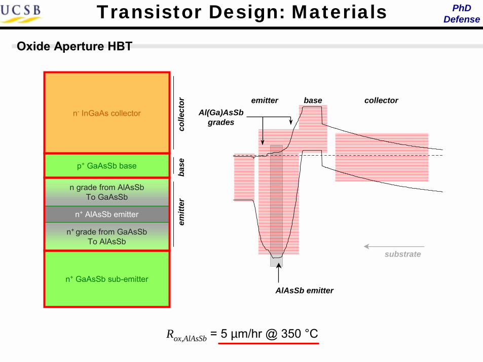
AlAsSb emitter
Transistor Design: MaterialsOxide Aperture HBT
n- InGaAs collector
p+ GaAsSb base
n grade from AlAsSbTo GaAsSb
n+ AlAsSb emitter
n+ grade from GaAsSbTo AlAsSb
n+ GaAsSb sub-emitter
baseemitterAl(Ga)AsSb
grades
collector
substrate
Rox,AlAsSb = 5 µm/hr @ 350 °C
emitt
erba
seco
llect
or

PhDDefenseGrowth of GaAsSb/AlAsSb
Two methods to grow GaAsSb/AlAsSb
Digital Alloy of III-As/III-Sb Analog Alloy
Shutter Cycles
III-As
III-Sb
Sb Sb
III III
xx
Φ∝Φ
Pros: Highly reproducibleCons: Heavy wear & tear
Pros: Greatly reduced wear & tearCons: Requires growth
calibrations, maintenance
Growth of AlxGa1-xAsySb1-y
A fully digital growth (III-As/III-Sb) is undesirable due to the wear & tearA fully analog growth is practically impossible, requiring cals for each compositionTherefore, a digital alloy of the analog alloys GaAsSb/AlAsSb is used to form the
grades between GaAsSb and AlAsSb
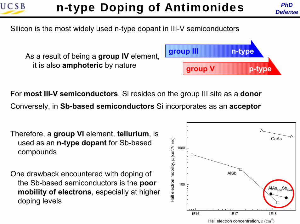
PhDDefensen-type Doping of Antimonides
Silicon is the most widely used n-type dopant in III-V semiconductors
group III n-type
group V p-typeAs a result of being a group IV element,
it is also amphoteric by nature
For most III-V semiconductors, Si resides on the group III site as a donorConversely, in Sb-based semiconductors Si incorporates as an acceptor
Therefore, a group VI element, tellurium, is used as an n-type dopant for Sb-based compounds
One drawback encountered with doping of the Sb-based semiconductors is the poor mobility of electrons, especially at higher doping levels
1E16 1E17 1E18
100
1000
AlAs0.56Sb0.44
AlSb
GaAs
Hal
l ele
ctro
n m
obilit
y, µ
(cm
2 /V se
c)
Hall electron concentration, n (cm-3)

PhDDefense
Introduction
Oxide Aperture HBTs
Growth as related to bipolar transistors Growth of GaAs0.49Sb0.51, AlAs0.56Sb0.44, and AlxGa1-xAsySb1-y
n-type doping of arsenide-antimonides
Current density: area versus perimeter Aperture placement Diode Selection Rules
Generation Ø Generation I Generation II RF results
Transistor Design and Growth
Oxide Aperture Diodes
Conclusions and Future Work
Introduction
Oxide Aperture HBTs
Growth as related to bipolar transistors Growth of GaAs0.49Sb0.51, AlAs0.56Sb0.44, and AlxGa1-xAsySb1-y
n-type doping of arsenide-antimonides
Generation Ø Generation I Generation II RF results
Transistor Design and Growth
Conclusions and Future Work
Overview
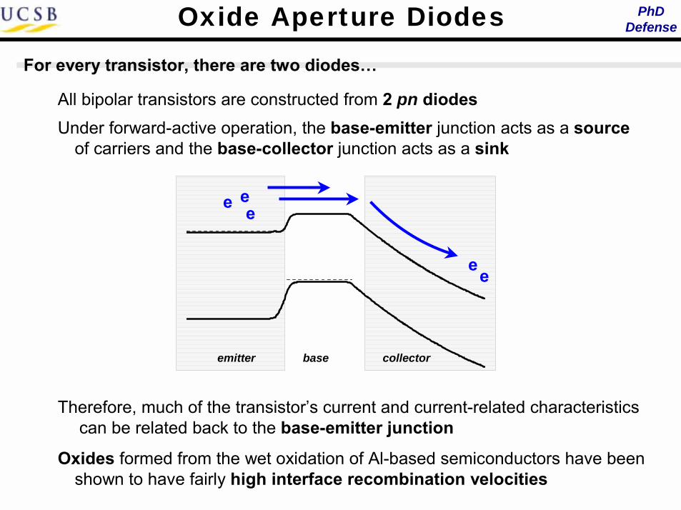
PhDDefenseOxide Aperture Diodes
For every transistor, there are two diodes
All bipolar transistors are constructed from 2 pn diodesUnder forward-active operation, the base-emitter junction acts as a source
of carriers and the base-collector junction acts as a sink
Therefore, much of the transistors current and current-related characteristics can be related back to the base-emitter junction
Oxides formed from the wet oxidation of Al-based semiconductors have been shown to have fairly high interface recombination velocities
ee e
ee
emitter base collector

PhDDefenseOxide Aperture Diodes
Oxide aperture diodes were fabricated to understand the potential effect of the oxide aperture on the current-voltage characteristics of the BE junction of the HBT
p+ GaAsSb base
n grade from AlAsSbTo GaAsSb
n+ AlAsSb emitter
n+ grade from GaAsSbTo AlAsSb
n+ GaAsSb sub-emitter
SI InP substrate
BE grade
emitter grade
tBE
2000 1500 1000 500 0-2.0
-1.6
-1.2
-0.8
-0.4
0.0
0.4
0.8
1.2
emittersub-emitter emittergrade BE grade base
E - E
F (eV
)
Distance from surface (Å)
Layer Structure Band Diagram
Three thickness of BE grade were examined: 100 Å, 500 Å, 1000 Å

PhDDefense
0.00 0.25 0.50 0.751E-16
1E-15
1E-14
1E-13
1E-12
1E-11
1E-10
1E-9
1E-8
1E-7
1E-6
1E-5
1E-4
K J
K (A
/µm
) and
J (A
/µm
2 )
V (V)
Current Density: A versus PIn addition to the ideality factor (η), the geometric dependence of the current
provides information on the nature of current conduction within a pn junction
In actual diodes, the total current can be written as a sum of an area dependent and perimeter dependent current measured j jI J A K P= ⋅ + ⋅
jmeasuredmeasured
j j
PIJ J KA A
= = + ⋅
0.1 0.2 0.3 0.4 0.5 0.6 0.7 0.8 0.90
5
10
15
20
25
increasing V
Vapp = 0.24 V Vapp = 0.30 V Vapp = 0.36 V
J = 0.15 nA/µm2
K = 3.02 nA/µm
J = 0.49 nA/µm2
K = 8.91 nA/µm
J = 1.87 nA/µm2
K = 28.6 nA/µm
I mea
sure
d / A
(nA
/µm
2 )
P / A (1/µm)0.0 0.1 0.2 0.3 0.4 0.5
0
2
4
ηk η j
Idea
lity
Fact
or
V (V)
For a given bias with Pj / Aj as the independent variable, J corresponds to the y-intercept and K to the slope of the equation
( )1j TV VSJ J e η= −
( )1k TV VSK K e η= −
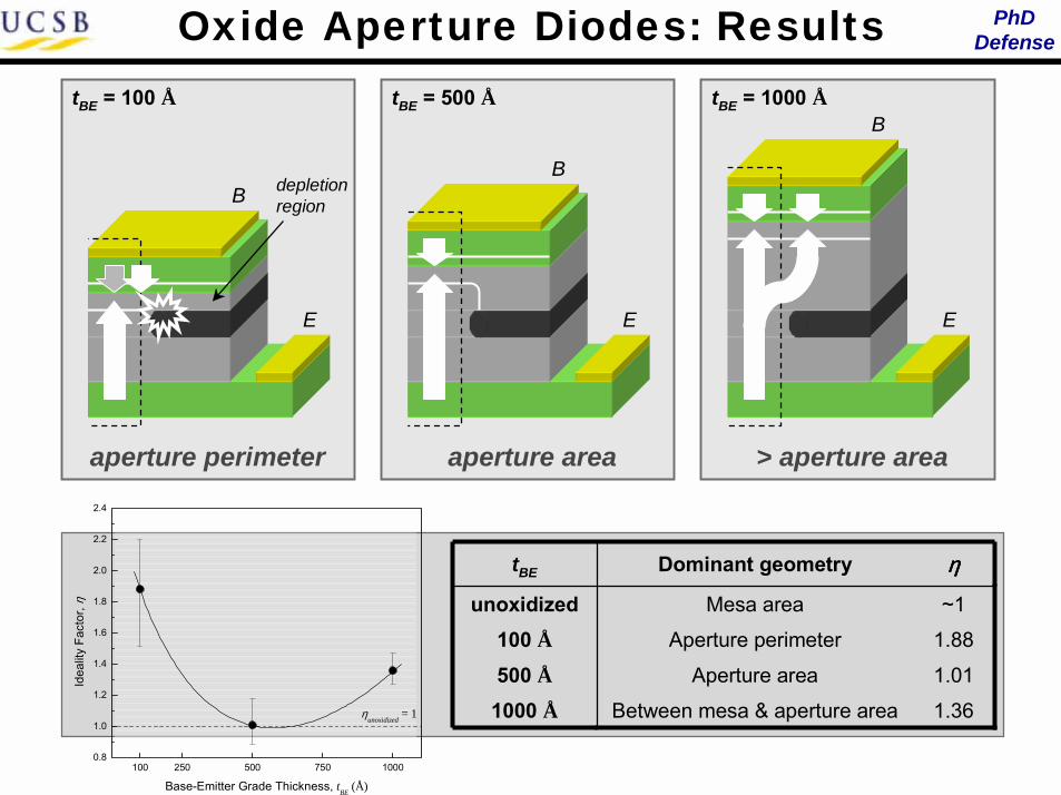
PhDDefenseOxide Aperture Diodes: Results
tBE = 100 Å
B
E
depletionregion
tBE = 500 Å
B
E
tBE = 1000 ÅB
E
100 250 500 750 10000.8
1.0
1.2
1.4
1.6
1.8
2.0
2.2
2.4
ηunoxidized = 1
Idea
lity
Fact
or, η
Base-Emitter Grade Thickness, tBE (Å)
aperture perimeter aperture area > aperture area
1.36Between mesa & aperture area1000 Å1.01Aperture area500 Å1.88Aperture perimeter100 Å~1Mesa areaunoxidized
ηηηηDominant geometrytBE

PhDDefenseOxide Aperture Diodes: Sims
Simulations performed using ATLAS simulation software generally agree with the experimental results
tBE = 1000 ÅtBE = 500 ÅtBE = 100 Å
Simulations performed without interface recombination
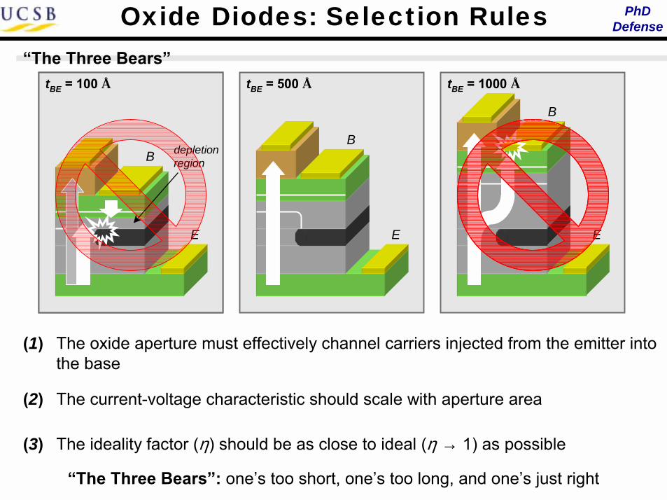
PhDDefenseOxide Diodes: Selection Rules
The Three Bears
(1) The oxide aperture must effectively channel carriers injected from the emitter into the base
(2) The current-voltage characteristic should scale with aperture area
(3) The ideality factor (η) should be as close to ideal (η → 1) as possible
The Three Bears:The Three Bears: ones too shortThe Three Bears: ones too short, ones too longThe Three Bears: ones too short, ones too long, and ones just right
B
E
depletionregion
tBE = 100 Å
B
E
tBE = 500 Å
B
E
tBE = 1000 Å
B
E
depletionregion
tBE = 100 Å

PhDDefenseOverview
Introduction
Oxide Aperture HBTs
Growth as related to bipolar transistors Growth of GaAs0.49Sb0.51, AlAs0.56Sb0.44, and AlxGa1-xAsySb1-y
n-type doping of arsenide-antimonides
Current density: area versus perimeter Aperture placement Diode Selection Rules
Generation Ø Generation I Generation II RF results
Transistor Design and Growth
Oxide Aperture Diodes
Conclusions and Future Work
Introduction
Growth as related to bipolar transistors Growth of GaAs0.49Sb0.51, AlAs0.56Sb0.44, and AlxGa1-xAsySb1-y
n-type doping of arsenide-antimonides
Current density: area versus perimeter Aperture placement Diode Selection Rules
Transistor Design and Growth
Oxide Aperture Diodes
Conclusions and Future Work

PhDDefenseOxide Aperture HBTs
Three generations of oxide aperture HBTs were fabricated:
Generation Ø: The first generation of oxide aperture HBTs, fabricated before the oxide aperture diode study
Generation I: The first generation of HBTs to show true transistor action, fabricated after the oxide aperture diode study
Generation II: The first generation of oxide aperture HBTs to produce high-frequency results
-2.0
-1.5
-1.0
-0.5
0.0
0.5
1.0 InGaAs collectorGa(Al)AsSb
emitterGaAsSb
base
E - E
F (eV
)
n- InGaAs collector
p+ GaAsSb base
n grade from AlAsSbTo GaAsSb
n+ AlAsSb emittern+ grade from GaAsSb
To AlAsSb
n+ GaAsSb sub-emitter
Laye
r Str
uctu
re
Ban
d D
iagr
am
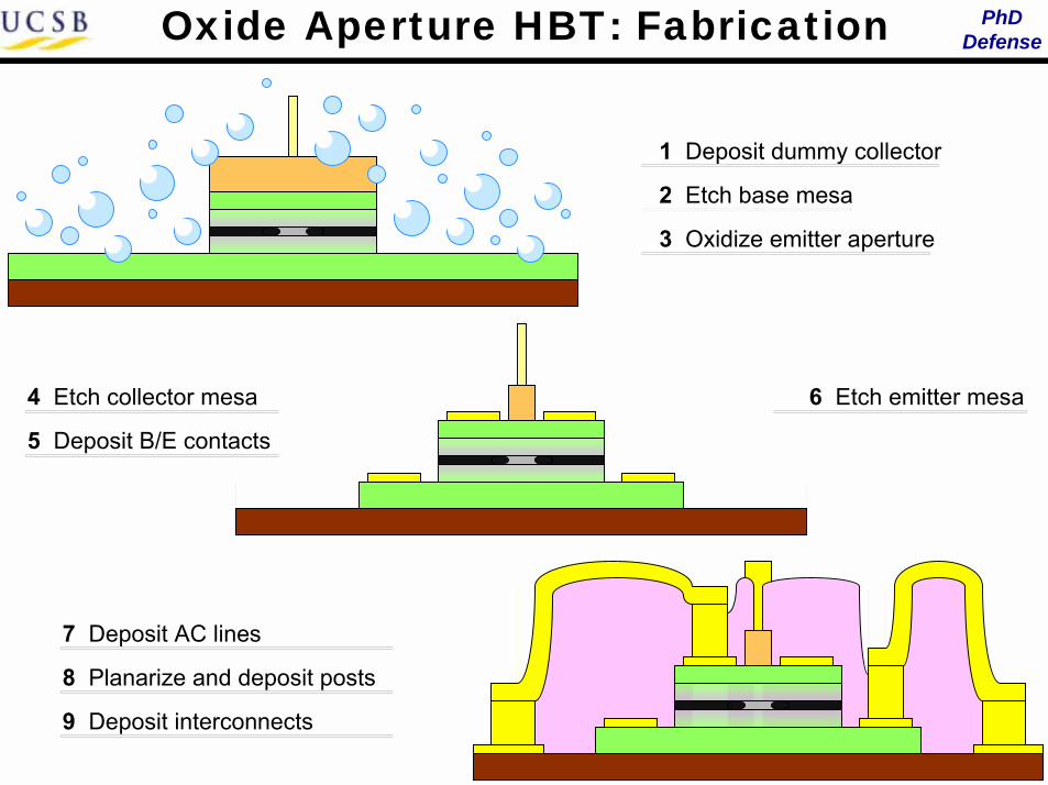
PhDDefenseOxide Aperture HBT: Fabrication
SiO2 dummy collector
1 Deposit dummy collector
2 Etch base mesa
3 Oxidize emitter aperture
4 Etch collector mesa
5 Deposit B/E contacts
6 Etch emitter mesa
7 Deposit AC lines
8 Planarize and deposit posts
9 Deposit interconnects
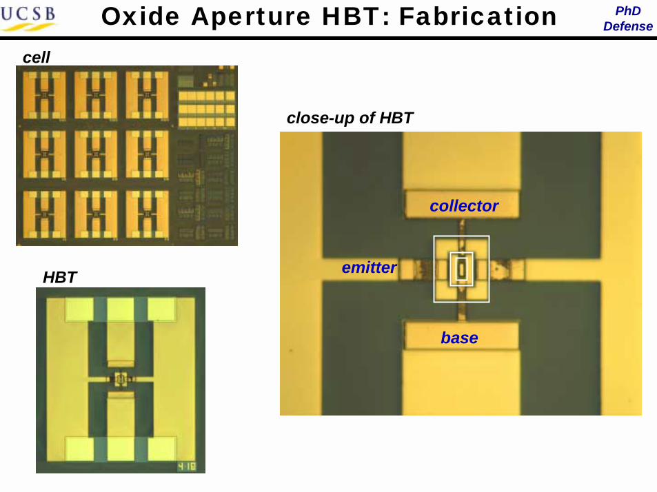
PhDDefenseOxide Aperture HBT: Fabrication
HBTs of various sizes
Misaligned HBTsTLMs
cell
CPW lines
HBT
cell
HBT
close-up of HBT
emitter
base
collector

PhDDefense
-1.5
-1.0
-0.5
0.0
0.5
1.0
1.5
2.0
Ga(Al)AsSbgrade
Ga(Al)AsSbemitter InGaAs collectorInGaAs
base
E - E
F (eV
)
Oxide HBTs: Generation Ø
Key Differences of Gen Ø HBT
InGaAs base Abrupt BE junction 2000 Å collector
η ≈ 1.7 β on the order of 10-6 ~ 10-5
Non-existent IC, low ββββ, and high ηηηη all suggest that the characteristic is recombination dominated
Results prompted the oxide diode study0.0 0.5 1.0 1.5 2.0 2.51E-11
1E-10
1E-9
1E-8
1E-7
1E-6
1E-5
1E-4
1E-3
0.01
0.1
IB IC
I B and
I C (A)
VBE (V)
0
2
4
6
8
10
12
14
β (10-6)
β

PhDDefenseOxide HBTs: Generation I
-2.0
-1.5
-1.0
-0.5
0.0
0.5
1.0 InGaAs collectorGa(Al)AsSb
emitterGaAsSb
base
E - E
F (eV
)
0.0 0.5 1.0 1.51E-7
1E-6
1E-5
1E-4
1E-3
0.01
I B and
I C (A)
VBE (V)
IB IC
0
25
50
75
100
β
β
0.00 0.25 0.50 0.75 1.00 1.25 1.50 1.750
2
4
6
8
10IB = 0 ~ 90 µA IB, step = 10 µA
I C (mA
)
VCE (V)
Key Differences of Gen I HBT
Lower doping in base and emitter 2000 Å collector
β ≈ 90
η ≈ 2.95
η ≈ 3.34
Fabricated from same material as the oxide diodes

PhDDefenseVoffset and Vknee
Voffset : VCE at which IC = 0
Vknee : VCE at which the device switches between forward-saturation and forward-active operation (VBC ≈ 0)
( ),
,
ln 1bc sat bc bcoffset bc BE B B B B
F be sat be be
IkTV V I R I Rq I
η ηηα η η
+ − − + !
( ) ( ), ,
ln ln1 1
be E R C bc F E Cknee E E C C
be sat F R bc sat F R
kT I I kT I IV I R I Rq I q I
η α η αα α α α
− −− + + − − !
Definitions
Vbkd
VoffsetVknee
VCE
IC
Modified Ebers-Moll Model
RB
RE RC
intrinsic model

PhDDefense
VCE
IC
VCE
IC
VCE
IC
VCE
IC
increasing RE
VCE
IC
The Knee Voltage: Vknee
( ) ( ), ,
ln ln1 1
be E R C bc F E Cknee E E C C
be sat F R bc sat F R
kT I I kT I IV I R I Rq I q I
η α η αα α α α
− −− + + − − !
0.00 0.25 0.50 0.75 1.00 1.25 1.50 1.750
2
4
6
8
10IB = 0 ~ 90 µA IB, step = 10 µA
I C (mA
)
VCE (V)
REVknee
Model Measured

PhDDefense
0.0 0.5 1.0 1.5 2.0 2.50.0
0.1
0.2
0.3
0.4
0.5
0.6
0.7
0.8
V CE (V
)
IB (mA)
Generation I HBT
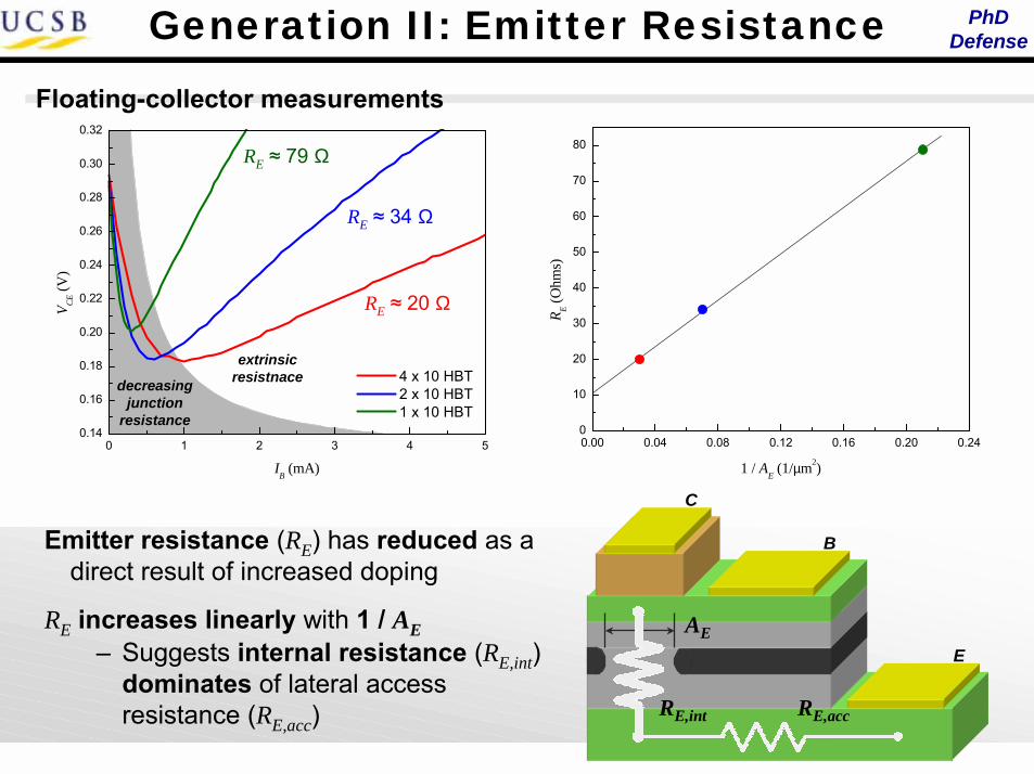
Generation I: Emitter Resistance
The emitter resistance (RE) of a bipolar transistor can be measured by floating-collector measurements
RE
RC
RB
IB
VCE
IB
VCE
REIB
0.0 0.5 1.0 1.5 2.0 2.50.0
0.1
0.2
0.3
0.4
0.5
0.6
0.7
0.8
V CE (V
)
IB (mA)
0
200
400
600
800
1000
RE (O
hms)
Generation I HBT
RE ≈ 85 ΩΩΩΩ
0.0 0.5 1.0 1.51E-11
1E-10
1E-9
1E-8
1E-7
1E-6
1E-5
1E-4
1E-3
0.01
0.1
I (A
)
V (V)
0
200
400
600
800
1000
rd (Ohm
s)
oxide diode
rd ≈ 75 ΩΩΩΩ
At a current level of ~4 mA with RE ≈ 85 ΩΩΩΩ ! Vknee ≥ 0.34 V

PhDDefenseOxide HBTs: Generation II
-2.0
-1.5
-1.0
-0.5
0.0
0.5
1.0 InGaAs collectorGa(Al)AsSb
emitterGaAsSb
base
E - E
F (eV
)
What have we learned so far
Generation Ø and oxide diodesOxide aperture placement is critical
Generation IResistance in the emitter due to the low electron mobility in AlAs0.56Sb0.44
is a problem (high Vknee)
Generation II
Oxide aperture is located 500 Å from the pn junction (same as Gen I)
Increased doping in the emitter and base
Increased collector width to 3000 Å
The Three Bears: cant be too close, cant be too far, has to be just right

PhDDefense
4 x 10 HBT2 x 10 HBT1 x 10 HBTAE = 3.5 x 9.5 µm2
AC = 4 x 10 µm2
Generation II: Gummel and CE
0.00 0.25 0.50 0.75 1.00 1.25 1.501E-11
1E-10
1E-9
1E-8
1E-7
1E-6
1E-5
1E-4
1E-3
0.01
0.1
IB IC
I B and
I C (A)
VBE (V)
0
1
2
3
4
β
β
0.0 0.2 0.4 0.6 0.8 1.0 1.20
1
2
3
4
IB = 0 ~ 1.5 mA IB, step = 150 µA
I C (mA
)
VCE (V)
0.00 0.25 0.50 0.75 1.00 1.25 1.501E-11
1E-10
1E-9
1E-8
1E-7
1E-6
1E-5
1E-4
1E-3
0.01
0.1
IB IC
I B and
I C (A)
VBE (V)
0
2
4
6
8
10
12
14
16
β
β
0.0 0.2 0.4 0.6 0.8 1.0 1.20
2
4
6
8
10
12
14
16IB = 0 ~ 1.25 mA IB, step = 125 µA
I C (mA
)
VCE (V)
0.00 0.25 0.50 0.75 1.001E-11
1E-10
1E-9
1E-8
1E-7
1E-6
1E-5
1E-4
1E-3
0.01
0.1 IB IC
I B and
I C (A)
VBE (V)
0
10
20
30
40
50
60
β
β
0.0 0.2 0.4 0.6 0.8 1.0 1.20
5
10
15
20
25
30IB = 0 ~ 0.5 mA IB, step = 50 µA
I C (mA
)
VCE (V)
AE = 0.5 x 9.5 µm2
AC = 1 x 10 µm2AE = 1.5 x 9.5 µm2
AC = 2 x 10 µm2
ββββ ≈ 2.6
ηηηη ≈ 1
ββββ ≈ 11
ηηηη ≈ 1
ββββ ≈ 40
ηηηη ≈ 1ηηηη ≈ 1.18ηηηη ≈ 1.18 ηηηη ≈ 1.18
PhDDefense
B
E
C
0.00 0.04 0.08 0.12 0.16 0.20 0.240
10
20
30
40
50
60
70
80
R E (Ohm
s)
1 / AE (1/µm2)
Generation II: Emitter Resistance
0 1 2 3 4 50.14
0.16
0.18
0.20
0.22
0.24
0.26
0.28
0.30
0.32
4 x 10 HBT 2 x 10 HBT 1 x 10 HBT
V CE (V
)
IB (mA)0 1 2 3 4 5
0.14
0.16
0.18
0.20
0.22
0.24
0.26
0.28
0.30
0.32
4 x 10 HBT 2 x 10 HBT 1 x 10 HBT
V CE (V
)
IB (mA)
Floating-collector measurements
RE ≈ 20 Ω
RE ≈ 34 Ω
RE ≈ 79 Ω
0.00 0.04 0.08 0.12 0.16 0.20 0.240
10
20
30
40
50
60
70
80
R E (Ohm
s)
1 / AE (1/µm2)
0.00 0.04 0.08 0.12 0.16 0.20 0.240
10
20
30
40
50
60
70
80
R E (Ohm
s)
1 / AE (1/µm2)
0.00 0.04 0.08 0.12 0.16 0.20 0.240
10
20
30
40
50
60
70
80
R E (Ohm
s)
1 / AE (1/µm2)
decreasing junction
resistance
extrinsic resistnace
RE,int RE,acc
Emitter resistance (RE) has reduced as a direct result of increased doping
RE increases linearly with 1 / AE Suggests internal resistance (RE,int)
dominates of lateral access resistance (RE,acc)
AE
PhDDefense
emitter
base
coll
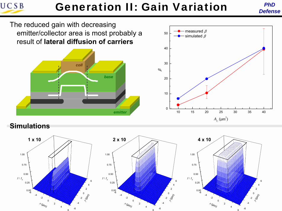
Generation II: Gain VariationThe reduced gain with decreasing
emitter/collector area is most probably a result of lateral diffusion of carriers
10 15 20 25 30 35 400
10
20
30
40
50
β
AC (µm2)
measured β
10 15 20 25 30 35 400
10
20
30
40
50
β
AC (µm2)
measured β simulated β
Simulations
-6-4
-20
24
6
0.00
0.25
0.50
0.75
1.00
-6
-4
-2
0
2
46
J / JE
y (µm
)
x (µm)
1 x 10
-6-4
-20
24
6
0.00
0.25
0.50
0.75
1.00
-6
-4
-2
0
2
46
J / JE
y (µm
)
x (µm)
2 x 10
-6-4
-20
24
6
0.00
0.25
0.50
0.75
1.00
-6
-4
-2
0
2
46
J / JE
y (µm
)
x (µm)
4 x 10

PhDDefense
Impact Ionization
Generation II: Output Conductance
0.0 0.5 1.0 1.50
5
10
15
20
25
30
I C (mA
)
VCE (V)
The output conductance (go) of the oxide aperture HBT is much higher than expected
The common-emitter breakdown voltage (Vbkd) is lower than expected
Early Effect
Early Effect
The Early effect (AKA base-width modulation) describes the increase in output current due to a change in the minority carrier profile in the base as a result of depletion at the BC junction
Only transistors with fairly low doped bases suffer from the Early Effect
-0.6 -0.4 -0.2 0.0 0.2 0.4 0.6 0.8 1.00.0
0.2
0.4
0.6
0.8
1.0
1.2
1.4
I C (A)
VCE (V)-0.6 -0.4 -0.2 0.0 0.2 0.4 0.6 0.8 1.0
0.0
0.2
0.4
0.6
0.8
1.0
1.2
1.4
I C (A)
VCE (V)-0.6 -0.4 -0.2 0.0 0.2 0.4 0.6 0.8 1.0
0.0
0.2
0.4
0.6
0.8
1.0
1.2
1.4
I C (A)
VCE (V)-0.6 -0.4 -0.2 0.0 0.2 0.4 0.6 0.8 1.0
0.0
0.2
0.4
0.6
0.8
1.0
1.2
1.4
I C (A)
VCE (V)
-VA
1E-4 1E-3
1
10
4 x 10 HBT 2 x 10 HBT 1 x 10 HBT
Extra
cted
VA (V
)
IB (A)
2 4 6 8 10101
102
103
104
105
GaAs InP InGaAs
α n (cm
-1)
Inverse electric field, 1/E (10-6 cm/V)
-0.8
-0.6
-0.4
-0.2
0.0
0.2
0.4
0.6
0.8
1.0
1.2
E - E
F (eV
)
e-
0.31 eVCE∆ !e- e-
h+
Impact Ionization

PhDDefense
E
B
C
E
B
C
Generation II: Misaligned HBTsIn conventional HBTs, the active collector area is larger than the active
emitter area
In oxide aperture HBTs, the active collector area and emitter area are roughly the same size
E
C
B
E
C
B
Aligned Misaligned
Aligned Misaligned

PhDDefense
+ 2 µµµµm
0.0 0.2 0.4 0.6 0.8 1.0 1.20.0
0.2
0.4
0.6
0.8
1.0
1.2
1.4
IB = 0 ~ 0.5 mA IB, step = 50 µA
I C (mA
)
VCE (V)
+ 1 µµµµm
0.0 0.2 0.4 0.6 0.8 1.0 1.20.0
0.2
0.4
0.6
0.8
1.0
1.2
1.4
IB = 0 ~ 0.5 mA IB, step = 50 µA
I C (mA
)
VCE (V)
Generation II: Misaligned HBTs
+ 0 µµµµm
0.00 0.25 0.50 0.75 1.001E-11
1E-10
1E-9
1E-8
1E-7
1E-6
1E-5
1E-4
1E-3
0.01
0.1 IB IC
I B and
I C (A)
VBE (V)
0
10
20
30
40
50
60
β
β
ββββ ≈ 400.00 0.25 0.50 0.75 1.00 1.25 1.50
1E-11
1E-10
1E-9
1E-8
1E-7
1E-6
1E-5
1E-4
1E-3
0.01
0.1 IB IC
I B and
I C (A)
VBE (V)
0.0
0.5
1.0
1.5
2.0
β
β
ββββ ≈ 1.250.00 0.25 0.50 0.75 1.00 1.25
1E-11
1E-10
1E-9
1E-8
1E-7
1E-6
1E-5
1E-4
1E-3
0.01
0.1 IB IC
I B and
I C (A)
VBE (V)
0.0
0.1
0.2
0.3
0.4
0.5
β
β
ββββ ≈ 0.25
0.0 0.2 0.4 0.6 0.8 1.0 1.20
5
10
15
20
25
30IB = 0 ~ 0.5 mA IB, step = 50 µA
I C (mA
)
VCE (V)0.0 0.2 0.4 0.6 0.8 1.0 1.2
0
5
10
15
20
25
30IB = 0 ~ 0.5 mA IB, step = 50 µA
I C (mA
)
VCE (V)
0.0 0.2 0.4 0.6 0.8 1.0 1.20.0
0.2
0.4
0.6
0.8
1.0
1.2
1.4
IB = 0 ~ 0.5 mA IB, step = 50 µA
I C (mA
)
VCE (V)0.0 0.2 0.4 0.6 0.8 1.0 1.2
0.0
0.2
0.4
0.6
0.8
1.0
1.2
1.4
IB = 0 ~ 0.5 mA IB, step = 50 µA
I C (mA
)
VCE (V)
AC = 4 x 10 µm2 and AE = 3.5 x 10 µm2 for all HBTsΙΒ = 0 ~ 0.5 mA at 50 µA steps

PhDDefenseRF Measurements
Scattering parameter (S-parameter) measurements were performed on the Generation II HBTs in order to evaluate the transistor's frequency performance
a1 a2
b1 b2
DUT
From S-parameters, characteristics like the short-circuit current gain (h21) and unilateral power gain (U) can be extracted
Subsequently, the current-gain cutoff frequency (fτ) and maximum frequency of oscillation (fmax) can be determined
1E8 1E9 1E100
2
4
6
8
10
12
14
16
18
20
22
h 21 a
nd U
(dB)
f (Hz)1E8 1E9 1E10
0
2
4
6
8
10
12
14
16
18
20
22
h 21 a
nd U
(dB)
f (Hz)
fττττ ≈ 8.3 GHzfmax ≈ 17.76 GHz
h21
U
PhDDefense
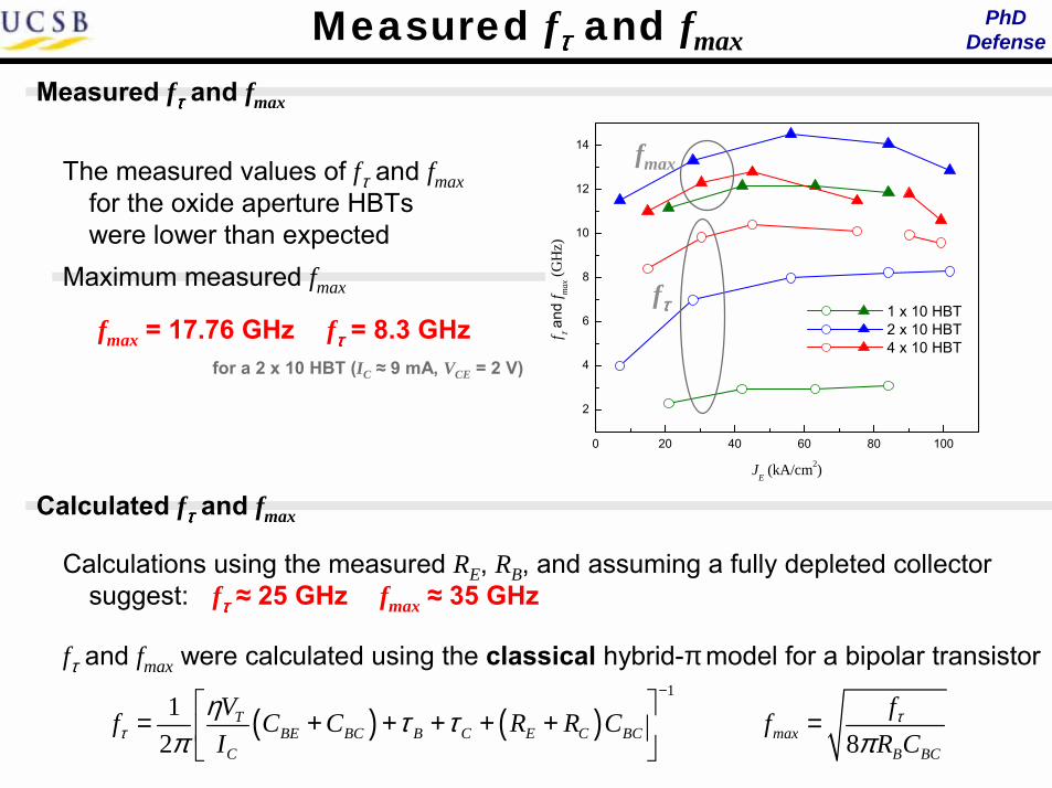
0 20 40 60 80 100
2
4
6
8
10
12
14
1 x 10 HBT 2 x 10 HBT 4 x 10 HBT
f τ and
f max
(GH
z)
JE (kA/cm2)
Measured fττττ and fmax
fmax
fττττ
The measured values of fτ and fmaxfor the oxide aperture HBTs were lower than expected
Measured fττττ and fmax
fττττ = 8.3 GHzfmax = 17.76 GHz
Maximum measured fmax
for a 2 x 10 HBT (IC ≈ 9 mA, VCE = 2 V)
Calculated fττττ and fmax
Calculations using the measured RE, RB, and assuming a fully depleted collector suggest: fττττ ≈ 25 GHz fmax ≈ 35 GHz
fτ and fmax were calculated using the classical hybrid-πmodel for a bipolar transistor
( ) ( )1
12
TBE BC B C E C BC
C
Vf C C R R CIτ
η τ τπ
−
= + + + + + 8max
B BC
ffR C
τ
π=
PhDDefense
B
E
CRCRB
RE
CBC
CDCBErπ
intrinsic
standard
gmvπ
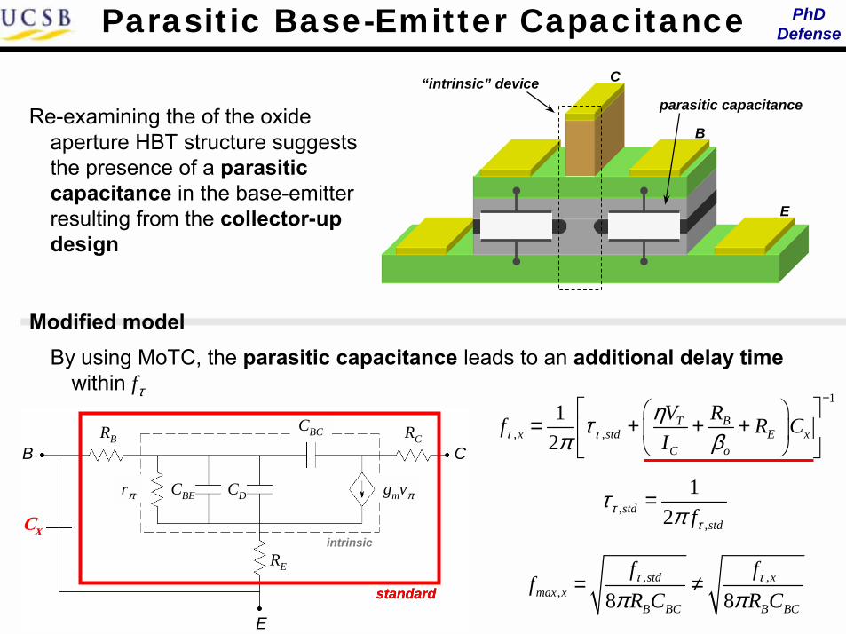
Parasitic Base-Emitter Capacitance
Re-examining the of the oxide aperture HBT structure suggests the presence of a parasitic capacitance in the base-emitter resulting from the collector-up design
E
C
B
“intrinsic” deviceparasitic capacitance
Modified modelBy using MoTC, the parasitic capacitance leads to an additional delay time
within fτ 1
, ,1
2T B
x std E xC o
V Rf R CIτ τ
ητπ β
−
= + + +
, ,, 8 8
std xmax x
B BC B BC
f ff
R C R Cτ τ
π π= ≠
,,
12std
stdfττ
τπ
=Cx
standard

PhDDefense
C
B
E
( ) ( )1
12
TBE BC B C E C BC
C
Vf C C R R CIτ
η τ τπ
−
= + + + + +
( )1
12
T E CBE E BC C B C BC C
C C E C
V r rf c A c A c AJ A A Aτη τ τ
π
−
= + + + + +
fττττ ScalingIn a transistor where AC ≈ AE, fτ should be essentially independent of emitter size
( ) ( )1
12
TBE BC B C E C BC
C
Vf c c r r cJτ
η τ τπ
−
= + + + + +
In the oxide aperture HBT, this is not true1
, ,1
2T B
x std E xC o
V Rf R CIτ τ
ητπ β
−
= + + +
0 5 10 15 20 25 30 352
4
6
8
10
12
measured
f t (GH
z)
AE (µm2)
Cx
wE
lE
0 5 10 15 20 25 30 352
4
6
8
10
12
measured modeled
f t (GH
z)
AE (µm2)
By applying the above equation, fτ,std = 1/2πττ,std ≈ 26.3 GHz and Cx ≈ 345 fF

PhDDefenseRF Device Modeling
Circuit designers require device models in order to design accurately and model circuits
Device models are useful to device engineers because they can lend insight into the operation of the device, in addition to verifying proposed phenomenon
Proper high-frequency model extraction requires:
(1) A well-behaved, stable device
(2) Y-parameters that accurately represent the device
Model Extraction
Y-parameters that accurately represent the transistor require prior knowledge of the model ??

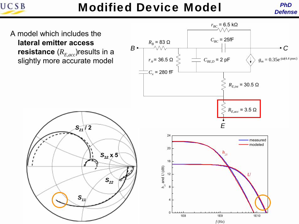
PhDDefenseDevice Model
Using measured characteristics (RB, RE, βo, gm) and initial estimates of other characteristics (rBC, CBC, Cx) a simple model was generated
rBC = 6.5 kΩ
RB = 83 Ω
RE = 34 Ω
Cx = 250 fF
rπ = 36.5 Ω CBE,D = 2 pF gm = 0.35e-jω(4.4 psec)
B C
E
CBC = 25fF
S11
S22
S21 / 2
S12 x 5
1E8 1E9 1E100
4
8
12
16
20
24
U
h21
measured
h 21 a
nd U
(dB)
f (Hz)1E8 1E9 1E10
0
4
8
12
16
20
24
U
h21
measured modeled
h 21 a
nd U
(dB)
f (Hz)
PhDDefense
1E8 1E9 1E100
4
8
12
16
20
24
U
h21
measured
h 21 a
nd U
(dB)
f (Hz)1E8 1E9 1E10
0
4
8
12
16
20
24
U
h21
measured modeled
h 21 a
nd U
(dB)
f (Hz)
Modified Device Model
S11
S22
S21 / 2
S12 x 5
rBC = 6.5 kΩ
RB = 83 Ω
RE,int = 30.5 Ω
Cx = 280 fF
rπ = 36.5 Ω CBE,D = 2 pF gm = 0.35e-jω(4.4 psec)
B C
E
CBC = 25fF
RE,acc = 3.5 Ω
A model which includes the lateral emitter access resistance (RE,acc)results in a slightly more accurate model
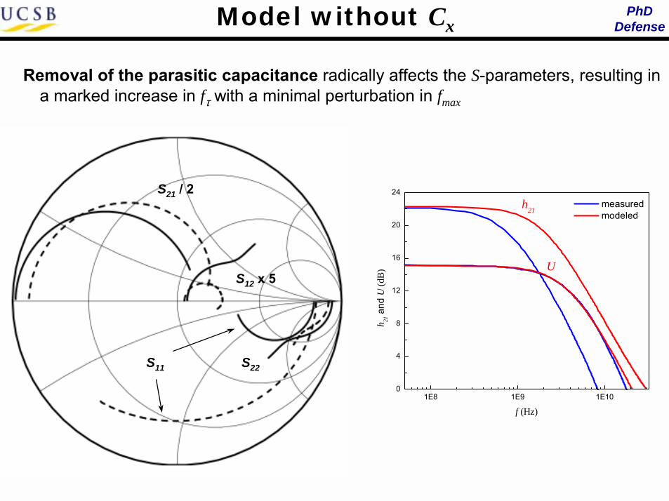
PhDDefenseModel without Cx
Removal of the parasitic capacitance radically affects the S-parameters, resulting in a marked increase in fτ with a minimal perturbation in fmax
S21 / 2
S12 x 5
S11 S22
1E8 1E9 1E100
4
8
12
16
20
24
U
h21 measured
h 21 a
nd U
(dB
)
f (Hz)1E8 1E9 1E10
0
4
8
12
16
20
24
U
h21 measured modeled
h 21 a
nd U
(dB
)
f (Hz)

PhDDefenseOverview
Introduction
Oxide Aperture HBTs
Growth as related to bipolar transistors Growth of GaAs0.49Sb0.51, AlAs0.56Sb0.44, and AlxGa1-xAsySb1-y
n-type doping of arsenide-antimonides
Current density: area versus perimeter Aperture placement Diode Selection Rules
Generation Ø Generation I Generation II RF results
Transistor Design and Growth
Oxide Aperture Diodes
Conclusions and Future Work
Introduction
Oxide Aperture HBTs
Growth as related to bipolar transistors Growth of GaAs0.49Sb0.51, AlAs0.56Sb0.44, and AlxGa1-xAsySb1-y
n-type doping of arsenide-antimonides
Current density: area versus perimeter Aperture placement Diode Selection Rules
Generation Ø Generation I Generation II RF results
Transistor Design and Growth
Oxide Aperture Diodes

PhDDefenseConclusions
The validity and application of the oxide aperture HBT design for high maximum frequency of oscillation (fmax) was examined
The work culminated with the fabrication of an oxide aperture HBT with an fτ on the order of 8 ~ 10 GHz and fmax of 12 ~ 17 GHz, with the maximum measured fmax being 17.76 GHz
Two critical aspects concerning the design and fabrication of the oxide aperture HBT became apparent:
(1) The impact of the oxide aperture on the DC operation of the BE junction and thereby the HBT
(2) The effect of the parasitic BE capacitance on the high-frequency performance of the HBT
The Three Bears
1
, ,1
2T B
x std E xC o
V Rf R CIτ τ
ητπ β
−
= + + +
PhDDefenseFuture Work
The research presented here represents a foundation
Suggested areas of research:
for reduced base-collector capacitance and increased fmax
sub-micron scaling
for reduced base transit times and increased fτbandgap graded base layers
Specific areas that must be examined in future research:
(1) collector designfor reduced output conductance and increased common-emitter breakdown
(2) base-emitter junction optimizationfor reduced emitter resistance and improved performance
(3) self-limiting oxidationfor sub-micron scaling and reduced parasitic base-emitter capacitance

PhDDefenseFuture Work
collector designThe high output conductance in the devices in this
work were attributed to impact ionization in the InGaAs collector
-1.2
-0.9
-0.6
-0.3
0.0
0.3
0.6
0.9
1.2
E - E
F (eV
)
-1.2
-0.9
-0.6
-0.3
0.0
0.3
0.6
0.9
1.2
E - E
F (eV
)A simple solution is to use an InP collector
Experiments by other groups have shown devices fabricated with this BC combination have increased output resistances and breakdown voltages
base-emitter junction designThe BE junction in this work is not the
optimum design
High RE due to low mobility AlAsSb in the emitterAlternatives:
InP-based emitterAlternative oxide source material: AlInAs
-2.0
-1.6
-1.2
-0.8
-0.4
0.0
0.4
0.8
1.2 Ga(Al)AsSbgrades
GaAsSbsub-emitter
GaAsSbbase
E - E
F (eV
)
-2.0
-1.6
-1.2
-0.8
-0.4
0.0
0.4
??
emitter GaAsSbbaseInPInP AlAsSb
E - E
F (eV
)

PhDDefenseFuture Work
self-limiting oxidationThe only means to control oxidation depth currently
is time and temperature
0 10 20 30 40 50 60 70 80 900
5
10
15
20
25
30
35
40
45 325 °C 350 °C 360 °C 375 °C
Oxi
datio
n de
pth,
d (µ
m)
Oxidation time, t (min)
This required the base mesa to be similar to and centered on the collector mesa
As a result, the oxide depth is equidistant from the outside edge of the oxidation mesa
oxide aperture HBT conventional HBT Possible Solutions
dox
dox
Stress/Strain Engineering:By inducing strain selectively under
the collector, it may be possible to alter the oxidation conditions
Selective Disordering:By generating disorder only outside
of the collector, it may be possible to increase the oxidation outside of the collector