Embed Size (px)
Citation preview

Highly integrated power electronic convertersusing active devices embedded in
printed-circuit board
Chenjiang YU1, Cyril BUTTAY2, Éric LABOURÉ1,Vincent BLEY3, Céline COMBETTES3
1GEEPS (LGEP), Paris, France2Laboratoire Ampère, Lyon, France
3 LAPLACE, Toulouse, France
17/4/15
1 / 23

Outline
Introduction
Review of PCB-based packaging
Proposed Embedding Technique
Summary and Conclusion
2 / 23
Outline
Introduction
Review of PCB-based packaging
Proposed Embedding Technique
Summary and Conclusion
3 / 23

Advantages of die embedding
The Printed-Circuit-Board technology (PCB) enables:
I higher interconnect densityI multi-layerI small pitch (down to 25 µm linewidth)
I Low inductance [1]I small sizeI laminated busbar structure
I batch-processed manufacturingI all interconnects are processed at once
E. Hoene, “Ultra Low Inductance Package for SiC” ECPEworkshop on power boards, 2012
4 / 23

Outline
Introduction
Review of PCB-based packaging
Proposed Embedding Technique
Summary and Conclusion
5 / 23

Literature Review – Converter on a flex substrate
Delft TU “folded” converter [2, 3]
images from ECPE Seminar “Power PCBs and Busbars”, Delft, 2008
I Use of a flex substrate to form windings,I wrapping around the larger componentsI thermal management might prove difficult
6 / 23

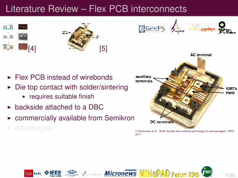
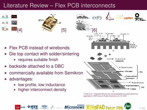
Literature Review – Flex PCB interconnects
[4]
[5] [6]
I Flex PCB instead of wirebondsI Die top contact with solder/sintering
I requires suitable finishI backside attached to a DBCI commercially available from SemikronI advantages:
I low profile, low inductanceI higher interconnect density
S. Dieckerhoff et al., “Electric Characteristics of Planar Interconnect Technologies forPower MOSFETs” PESC 2007
7 / 23
Literature Review – Flex PCB interconnects
[4] [5]
[6]
I Flex PCB instead of wirebondsI Die top contact with solder/sintering
I requires suitable finishI backside attached to a DBCI commercially available from SemikronI advantages:
I low profile, low inductanceI higher interconnect density
T. Stockmeier et al. “SKiN: Double side sintering technology for new packages”, ISPD2011
7 / 23
Literature Review – Flex PCB interconnects
[4] [5] [6]
I Flex PCB instead of wirebondsI Die top contact with solder/sintering
I requires suitable finishI backside attached to a DBCI commercially available from SemikronI advantages:
I low profile, low inductanceI higher interconnect density
Y. Xiao et al., “Integrated flip-chip flex-circuit packaging for power electronicsapplications”, IEEE trans on Power Electronics vol. 19, 2004
7 / 23

Literature Review – “PCB-like” 3D structures
P. Ning et al. “A novel high-temperature planar package for SiC multichip phase-leg powermodule”, IEEE Trans on PE vol 25, 2010, 25, 2059
Silver-sintered interconnects andEpoxy/Kapton insulation [7]
Weidner, et al. “Planar Interconnect Technology for Power Module System Integration”, CIPS2012
SiPLIT Copper electroplating,laminated isolation laser-structuredin-situ [8]
8 / 23

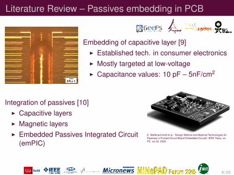
Literature Review – Passives embedding in PCB
Andresakis, J. “Embedded Capacitors” Oak-Mitsui Technologies,2005
Embedding of capacitive layer [9]I Established tech. in consumer electronicsI Mostly targeted at low-voltageI Capacitance values: 10 pF – 5nF/cm2
Integration of passives [10]I Capacitive layersI Magnetic layersI Embedded Passives Integrated Circuit
(emPIC)
E. Waffenschmidt et al. “Design Method and Material Technologies forPassives in Printed Circuit Board Embedded Circuits” IEEE Trans. onPE, vol 20, 2005
9 / 23
Literature Review – Passives embedding in PCB
Andresakis, J. “Embedded Capacitors” Oak-Mitsui Technologies,2005
Embedding of capacitive layer [9]I Established tech. in consumer electronicsI Mostly targeted at low-voltageI Capacitance values: 10 pF – 5nF/cm2
Integration of passives [10]I Capacitive layersI Magnetic layersI Embedded Passives Integrated Circuit
(emPIC)E. Waffenschmidt et al. “Design Method and Material Technologies forPassives in Printed Circuit Board Embedded Circuits” IEEE Trans. onPE, vol 20, 2005
9 / 23
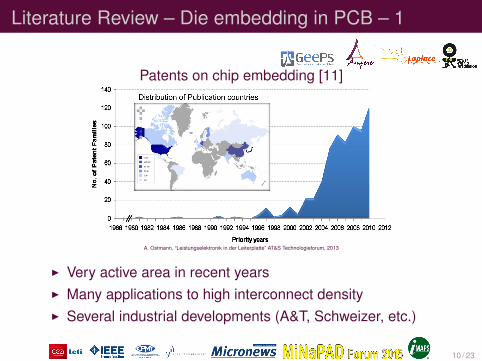
Literature Review – Die embedding in PCB – 1
Patents on chip embedding [11]
A. Ostmann, “Leistungselektronik in der Leiterplatte” AT&S Technologieforum, 2013
I Very active area in recent yearsI Many applications to high interconnect densityI Several industrial developments (A&T, Schweizer, etc.)
10 / 23

Literature Review – Die embedding in PCB – 2
Low-inductance packaging for SiC [1]I Half bridge moduleI 0.8 nH loop inductanceI Embedding die using stud bumps
E. Hoene, “Ultra Low Inductance Package for SiC” ECPE workshop on powerboards, 2012
I Power module development through germanproject Hi-LEVEL [12]
I 10 kW and 50 kW demonstratorsI Thick copper or DBC for thermal management
http://www.pcdandf.com/pcdesign/index.php/editorial/menu-features/9257-component-packaging-1405
11 / 23

Literature Review – Considerations on CAD tools
CAD tools with embedding capability [13]I Automatic placement of partsI Design rules (cavity size, height check, etc.)I Generation of the manufacturing data
I Position of dies, cavities, laser drilling, etc.
source: M. Brizoux et al. “Development of a Design& Manufacturing Environment for Reliable andCost-Effective PCB Embedding Technology” IPCApex, 2011
12 / 23
Outline
Introduction
Review of PCB-based packaging
Proposed Embedding Technique
Summary and Conclusion
13 / 23

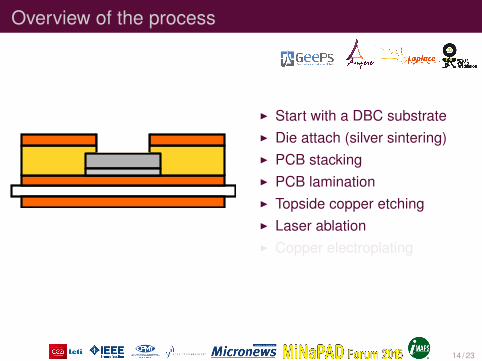
Overview of the process
I Start with a DBC substrateI Die attach (silver sintering)I PCB stackingI PCB laminationI Topside copper etchingI Laser ablationI Copper electroplating
14 / 23

Overview of the process
I Start with a DBC substrateI Die attach (silver sintering)I PCB stackingI PCB laminationI Topside copper etchingI Laser ablationI Copper electroplating
14 / 23

Overview of the process
I Start with a DBC substrateI Die attach (silver sintering)I PCB stackingI PCB laminationI Topside copper etchingI Laser ablationI Copper electroplating
14 / 23

Overview of the process
I Start with a DBC substrateI Die attach (silver sintering)I PCB stackingI PCB laminationI Topside copper etchingI Laser ablationI Copper electroplating
14 / 23

Overview of the process
I Start with a DBC substrateI Die attach (silver sintering)I PCB stackingI PCB laminationI Topside copper etchingI Laser ablationI Copper electroplating
14 / 23
Overview of the process
I Start with a DBC substrateI Die attach (silver sintering)I PCB stackingI PCB laminationI Topside copper etchingI Laser ablationI Copper electroplating
14 / 23

Overview of the process
I Start with a DBC substrateI Die attach (silver sintering)I PCB stackingI PCB laminationI Topside copper etchingI Laser ablationI Copper electroplating
14 / 23

Overview of the process – significant points
I Backside die attach with silver sintering:I The die does not move during assemblyI Accurate positioning
I Ablation using a CO2 laserI Very good selectivity (metal layers insensitive to laser light)I Use of the copper layer as an alignment mask
I Prototype-scale equipment usedI Can manufacture prototypes from 4x4 cm2 up to 21x28 cm2
I Affordable, useful for process development.
15 / 23

Effect of die finish
DieMask
PVD
Two die finishes evaluatedI standard Al topsideI Ti/Cu PVD with a shadow
mask 0.0 0.5 1.0 1.5 2.0 2.5 3.0Displacement [mm]
−5
0
5
10
15
20
25
30
Hei
ght[
µm
]
initial10 mins electroplating on Cu10 mins electroplating
16 / 23
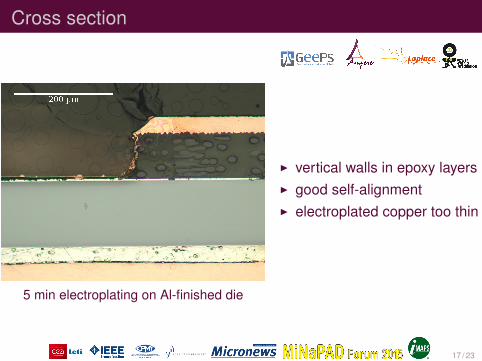
Cross section
5 min electroplating on Al-finished die
I vertical walls in epoxy layersI good self-alignmentI electroplated copper too thin
17 / 23

Electrical Characterization
0.0 0.5 1.0 1.5 2.0Forward Voltage [V]
0
10
20
30
40
50
60
Forw
ard
Cur
rent
[A]
Die with Al finish, 20 min electroplating
−1200 −1000 −800 −600 −400 −200 0Reverse voltage [V]
10−8
10−7
10−6
10−5
Rev
erse
curr
ent[
A]
I Tests performed in air, without additional passivationI die finish and electroplating time have a strong effect on
characteristic
18 / 23

Electrical Characterization
0.0 0.5 1.0 1.5 2.0Forward Voltage [V]
0
10
20
30
40
50
60
Forw
ard
Cur
rent
[A]
Die with Al finish, 20 min electroplatingDie with Cu finish, 20 min electroplatingDie with Al finish, 5 min electroplating
−1200 −1000 −800 −600 −400 −200 0Reverse voltage [V]
10−8
10−7
10−6
10−5
Rev
erse
curr
ent[
A]
I Tests performed in air, without additional passivationI die finish and electroplating time have a strong effect on
characteristic
18 / 23

Outline
Introduction
Review of PCB-based packaging
Proposed Embedding Technique
Summary and Conclusion
19 / 23

Summary and Conclusion
I Active developments on PCB-embeddingI Scalable technologyI Allows for more compact systemsI Attractive for fast, wide-bandgap devices
I Presentation of a prototype-scale processI Full details in the paper!I First results on large-die diode embedding
I Developments to come: embedding of an IGBT/diode halfbridge:
I Simple generation of all files from CAD (prepreg cutouts,dies opening. . . )
I Validation of alignment accuracy with the gate of the IGBTI Patterning of topside, mounting of SMT components
20 / 23

Bibliography I
E. Hoene, “Ultra Low Inductance Package for SiC,” in ECPE workshop on powerboards, ECPE, 2012.
E. de Jong, E. de Jong, B. Ferreira, and P. Bauer, “Toward the Next Level of PCBUsage in Power Electronic Converters,” Power Electronics, IEEE Transactions on,vol. 23, no. 6, pp. 3151–3163, 2008.
B. Ferreira, “PCB Integration Technology Overview,” in ECPE Seminar “PowerPCBs and Busbars”, (Delft), 2008.
S. Dieckerhoff, T. Kirfe, T. Wernicke, C. Kallmayer, A. Ostmann, E. Jung,B. Wunderle, and H. Reichl, “Electric Characteristics of Planar InterconnectTechnologies for Power MOSFETs,” in Power Electronics Specialists Conference,2007. PESC 2007. IEEE, pp. 1036 –1042, jun 2007.
T. Stockmeier, P. Beckedahl, C. Gobl, and T. Malzer, “SKiN: Double side sinteringtechnology for new packages,” in Power Semiconductor Devices and ICs(ISPSD), 2011 IEEE 23rd International Symposium on, pp. 324–327, May 2011.
Y. Xiao, H. Shah, R. Natarajan, E. J. Rymaszewski, T. Chow, and R. Gutmann,“Integrated flip-chip flex-circuit packaging for power electronics applications,”Power Electronics, IEEE Transactions on, vol. 19, pp. 515–522, March 2004.
21 / 23

Bibliography II
P. Ning, T. G. Lei, F. Wang, G.-Q. Lu, K. D. Ngo, and K. Rajashekara, “A novelhigh-temperature planar package for SiC multichip phase-leg power module,”Power Electronics, IEEE Transactions on, vol. 25, no. 8, pp. 2059–2067, 2010.
K. Weidner, M. Kaspar, and N. Seliger, “Planar Interconnect Technology forPower Module System Integration,” in Integrated Power Electronics Systems(CIPS), 2012 7th International Conference on, pp. 1–5, IEEE, 2012.
J. Andresakis, “Embedded Capacitors,” presentation, Oak-Mitsui Technologies,nov 2005.
E. Waffenschmidt, B. Ackermann, and J. A. Ferreira, “Design Method andMaterial Technologies for Passives in Printed Circuit Board Embedded Circuits,”IEEE Transactions on Power Electronics, vol. 20, pp. 576–584, may 2005.
A. Ostmann, “Leistungselektronik in der Leiterplatte,” in AT&S Technologieforum,2013.
A. Ostmann, L. Boettcher, D. Manessis, S. Karaszkiewicz, and K.-D. Lang,“Power modules with embedded components,” in Microelectronics PackagingConference (EMPC) , 2013 European, pp. 1–4, Sept 2013.
M. Brizoux, A. Grivon, W. Maia Filho, et al., “Development of a Design &Manufacturing Environment for Reliable and Cost-Effective PCB EmbeddingTechnology,” in IPC Apex Expo conference, 2011.
22 / 23
Thank you for your attention
This work was funded by the French National Research Agency(ANR) under the grant name ETHAER.The authors thank Mr Gilles BRILLAT for his technical help.
23 / 23