Embed Size (px)
Citation preview

Innovative solutions for tomorrows challenges
©2012 Renesas Mobile Corporation. All rights reserved.1
High Speed Mixed Signal PCB DesignSome Practical Considerations
Séminaire Telecom ParisTech, Paris, France03/05/2012
Renesas Mobile Corporation
Yann Le Guillou, PhDRF Platform Lead [email protected]

©2012 Renesas Mobile Corporation. All rights reserved.2
Renesas Mobile is well placed to help customers maximise the potential of the wireless revolution by delivering ground breaking solutions that drive the wide adoption of LTEmulti-mode devices into high volume segments from smartphones and tablets to embedded devices
Our portfolio of solutions to OEMs and ODMs worldwide includes:-
Versatile and flexible Mobile Platforms High performance Application processors Highly integrated Slim multi-mode cellular modems
Renesas Mobile - What We Do…
©2012 Renesas Mobile Corporation. All rights reserved.3
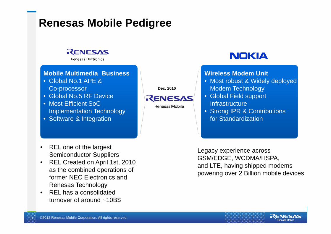
Renesas Mobile Pedigree
Dec. 2010
• REL one of the largest Semiconductor Suppliers
• REL Created on April 1st, 2010 as the combined operations of former NEC Electronics and Renesas Technology
• REL has a consolidated turnover of around ~10B$
Legacy experience across GSM/EDGE, WCDMA/HSPA, and LTE, having shipped modems powering over 2 Billion mobile devices
Mobile Multimedia Business• Global No.1 APE &
Co-processor• Global No.5 RF Device• Most Efficient SoC
Implementation Technology• Software & Integration
Wireless Modem Unit• Most robust & Widely deployed
Modem Technology• Global Field support
Infrastructure• Strong IPR & Contributions
for Standardization

©2012 Renesas Mobile Corporation. All rights reserved.4
Renesas Mobile’s Worldwide Presence
FINLANDHelsinki
OuluTampere
Salo
INDIABangalore
USASan Diego
Irving
TAIWANTaipei
DENMARKCopenhagen
UKFarnborough
CHINABeijing
Shanghai
GERMANYMunich
JAPANTokyo, RMC HQ
TakasakiKodairaNagoya
FRANCERennesParis
KOREASeoul
©2012 Renesas Mobile Corporation. All rights reserved.5
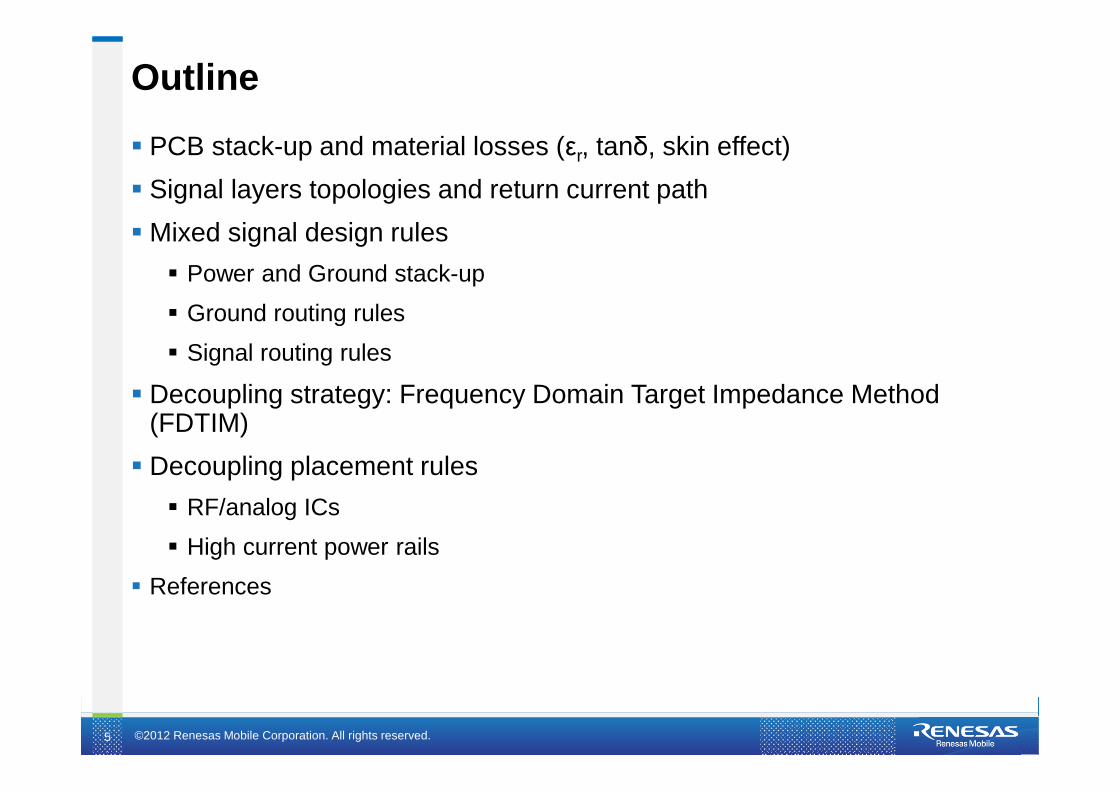
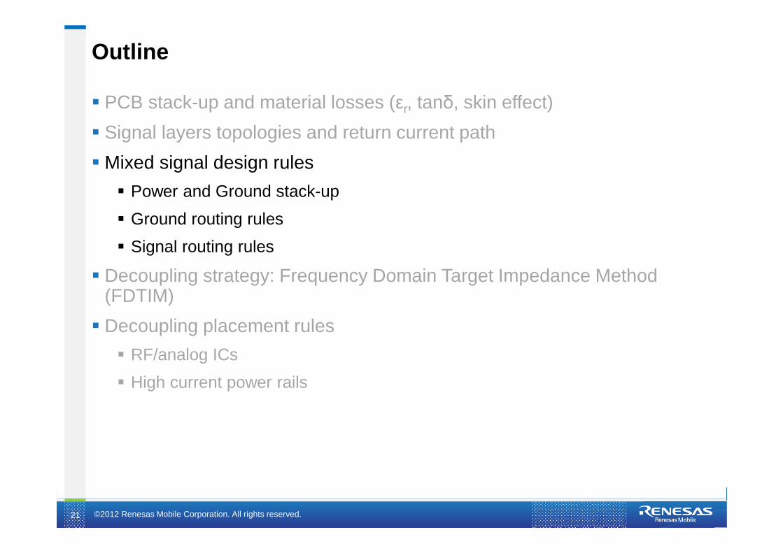
Outline
PCB stack-up and material losses (εr, tanδ, skin effect)
Signal layers topologies and return current path
Mixed signal design rules
Power and Ground stack-up
Ground routing rules
Signal routing rules
Decoupling strategy: Frequency Domain Target Impedance Method (FDTIM)
Decoupling placement rules
RF/analog ICs
High current power rails
References

©2012 Renesas Mobile Corporation. All rights reserved.6
PCB constructed from multiple alternating layers of core, prepreg and copper foil materials heat-pressed and glued together.
Example of a 10-layers PCB stack-up
Core: hardened fiber glass-
weaves material with epoxy resin. It acts as an insulation layer between the copper foils.
Prepreg: non-hardened fiber
glass-weaves material with epoxy resin. It acts as an insulation layer between core layers and is the gluing agent for the cores
PCB stack-up construction

©2012 Renesas Mobile Corporation. All rights reserved.7
Signal layers: Layer count estimation
In high density BGAs, many signal layers are required to achieve full break of all available IOs
Estimation of the minimum number of layers Nmin required for a balancedPCB stack-up:
( ) ( )
( ) ( )
+
=oddis
2columndepth,rowdepthmax
if,12
columndepth,rowdepthmax
evenis2
columndepth,rowdepthmaxif,
2columndepth,rowdepthmax
Nmin
Example: Xilinx Virtex 5 SXT in a FF665 BGA package:
Nmin=8
13 columns deep
13 rows deep
©2012 Renesas Mobile Corporation. All rights reserved.8
Material loss consideration: Relative dielectric constant εr εr is a measure of material’s ability :
to be polarized by an electric field and store electrostatic energy to facilitate signal propagation. The higher the relative dielectric constant:
• the slower a signal travels on a wire,• the lower the impedance of a given trace geometry • the larger the stray capacitance along a transmission line.
εr is generally an inverse function of its frequency. Digital signals are comprised of many harmonics The impedance of a transmission line goes down as frequency goes up
resulting in faster edges reflecting more than slower ones. Differences in impedance for RF Broadband can cause signal loss from both
reflections and phase distortion (phase jitter) arising from the different frequencies arriving at the destination at different times
Always choose lower εr material with flat frequency response for best signal performance and to minimize signal dist ortion and phase jitter especially for broadband RF and high speed a pplications

©2012 Renesas Mobile Corporation. All rights reserved.9
Material loss consideration : loss tangent tan( δ)
tan(δ) is a measure of signal loss as the signal propagatesdown the trasmission line.
It is the result of electromagnetic wave absorption by the dielectric material and depends on the material’s structure and glass-resin composition
A lower tan( δ) results in more of the original transmittedsignal getting through to its destination.
Attenuation can be calculated according to:
[ ] ( ) r.tan.f.4.23.2
cm.dBnAttenuatio εδ=
f is the frequency in GHz tan(δ) is the dimensionless loss tangent εr is the relative dielectric constant of the material

©2012 Renesas Mobile Corporation. All rights reserved.10
Comparison of loss tangent attenuation
Example: Trace length 10 cm Design running at 240MSps (I,Q data time interleaved) Nyquist equivalent frequency is 120MHz Loss due to the dielectric absorption of :
• Typical FR4 is 0.0046dB per cm and ≈0.05dB for 10cm trace length• Hitachi MCL-LX-67Y is 5 times smaller and ≈0.01dB for 10cm trace length.
Material εεεεr tan( δδδδ)Typical FR4 4 0,02GETEK 3,9 0,01Isola 370HR 4,17 0,016Isola FR406 4,29 0,014Isola FR08 3,7 0,011Hitachi MCL-LX-67Y 3,4 0,005Megtron 6 3,4 0,002Nelco 4000-6 4,12 0,012Nelco 4000-13 EP 3,7 0,009Nelco 4000-13 EP SI 3,2 0,008Rogers 4350B 3,48 0,0037
©2012 Renesas Mobile Corporation. All rights reserved.11
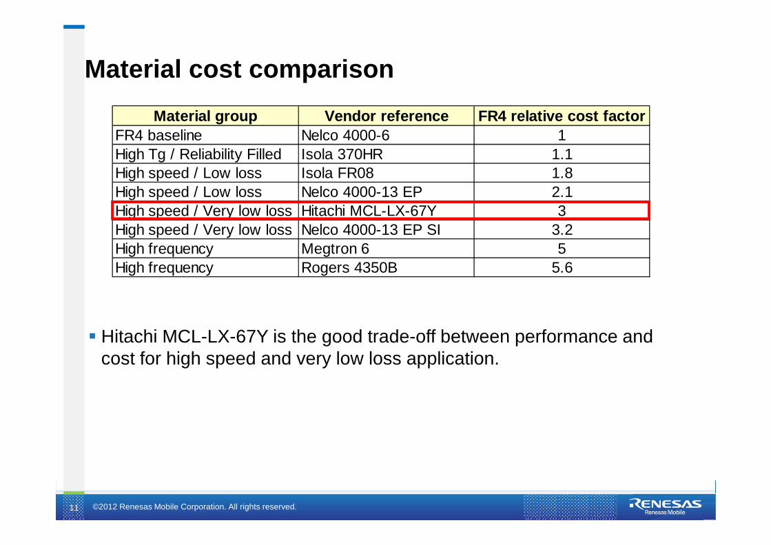
Material cost comparison
Hitachi MCL-LX-67Y is the good trade-off between performance and cost for high speed and very low loss application.
Material group Vendor reference FR4 relative cost fac torFR4 baseline Nelco 4000-6 1High Tg / Reliability Filled Isola 370HR 1.1High speed / Low loss Isola FR08 1.8High speed / Low loss Nelco 4000-13 EP 2.1High speed / Very low loss Hitachi MCL-LX-67Y 3High speed / Very low loss Nelco 4000-13 EP SI 3.2High frequency Megtron 6 5High frequency Rogers 4350B 5.6
©2012 Renesas Mobile Corporation. All rights reserved.12
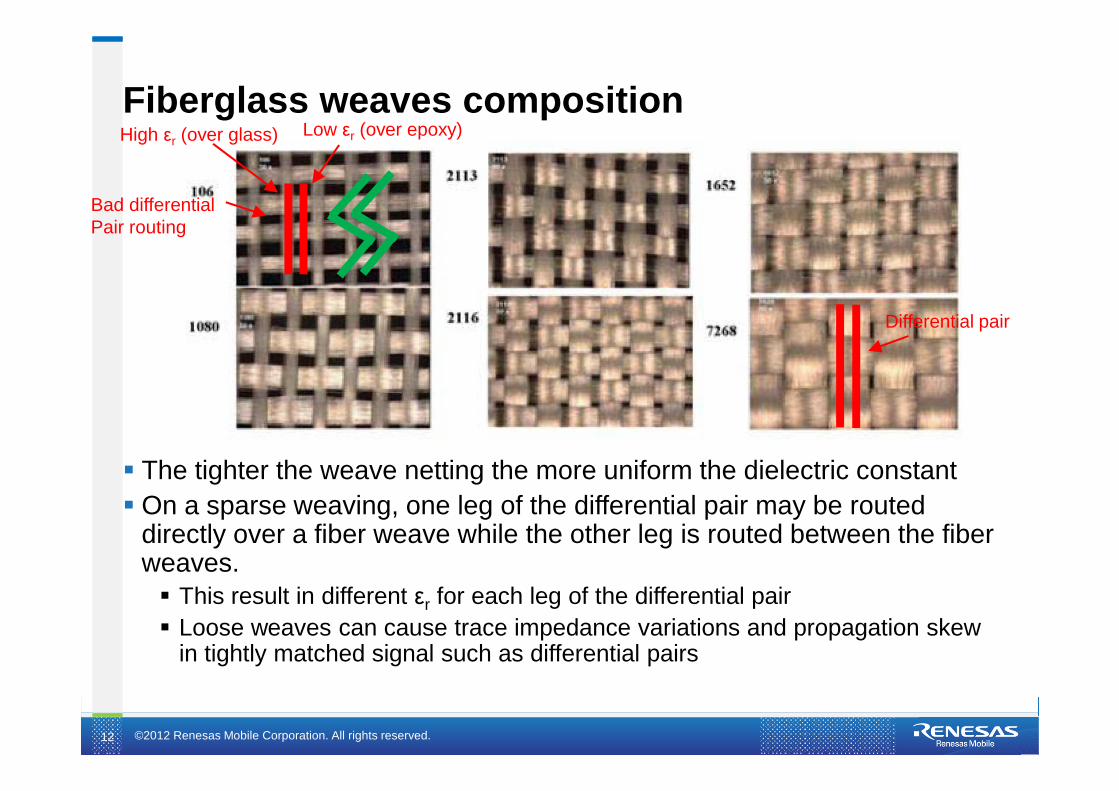
Fiberglass weaves composition
The tighter the weave netting the more uniform the dielectric constant On a sparse weaving, one leg of the differential pair may be routed
directly over a fiber weave while the other leg is routed between the fiber weaves. This result in different εr for each leg of the differential pair Loose weaves can cause trace impedance variations and propagation skew
in tightly matched signal such as differential pairs
Bad differentialPair routing
Differential pair
High εr (over glass) Low εr (over epoxy)
©2012 Renesas Mobile Corporation. All rights reserved.13
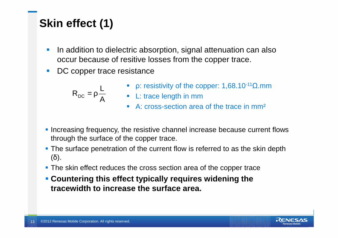
Skin effect (1)
In addition to dielectric absorption, signal attenuation can alsooccur because of resitive losses from the copper trace.
DC copper trace resistance
AL
RDC ρ= ρ: resistivity of the copper: 1,68.10-11Ω.mm L: trace length in mm A: cross-section area of the trace in mm²
Increasing frequency, the resistive channel increase because current flowsthrough the surface of the copper trace.
The surface penetration of the current flow is referred to as the skin depth(δ).
The skin effect reduces the cross section area of the copper trace
Countering this effect typically requires widening the tracewidth to increase the surface area.

©2012 Renesas Mobile Corporation. All rights reserved.14
2 062,88
652,34
206,29
65,23
20,63
6,52
2,061
10
100
1000
10000
1E+3 10E+3 100E+3 1E+6 10E+6 100E+6 1E+9
δ [µ
m]
frequency [Hz]
Skin effect (2) Skin depth
f1
10.23,65f1
...
3
r0
−≈µµπ
ρ=δ
δ: skin depth in mm f: frequency in MHz ρ: resistivity of the copper: 1,68.10-10Ω. mm µ0=4.π.10-10H.mm-1
µr=1 relative permeability of nonmagnetic material
Copper trace resistance
WL
RAC δρ= δ: skin depth in mm
ρ: resistivity of the copper: 1,68.10-11Ω. mm
L: trace length in mm W: trace width in mm
Based on the skin depth value for a signal frequency f, signal traces must be sized appropriately to reduce losses because of the skin effect
122,79
38,83
12,28
3,88
1,23
0,39
0,120
1
10
100
1000
1E+3 10E+3 100E+3 1E+6 10E+6 100E+6 1E+9(L
/W).
10-6
ratio
, R
AC=1
mΩΩ ΩΩ
frequency [Hz]
©2012 Renesas Mobile Corporation. All rights reserved.15
Outline
PCB stack-up and material losses (εr, tanδ, skin effect)
Signal layers topologies and return current path
Mixed signal design rules
Power and Ground stack-up
Ground routing rules
Signal routing rules
Decoupling strategy: Frequency Domain Target Impedance Method (FDTIM)
Decoupling placement rules
RF/analog ICs
High current power rails
References
©2012 Renesas Mobile Corporation. All rights reserved.16
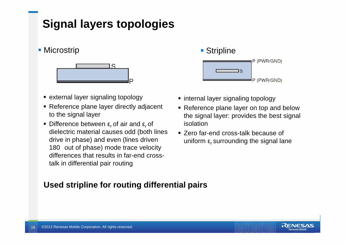
Signal layers topologies
Microstrip Stripline
external layer signaling topology Reference plane layer directly adjacent
to the signal layer Difference between εr of air and εr of
dielectric material causes odd (both lines drive in phase) and even (lines driven 180 out of phase) mode trace velocity differences that results in far-end cross-talk in differential pair routing
internal layer signaling topology Reference plane layer on top and below
the signal layer: provides the best signal isolation
Zero far-end cross-talk because of uniform εr surrounding the signal lane
Used stripline for routing differential pairs
©2012 Renesas Mobile Corporation. All rights reserved.17
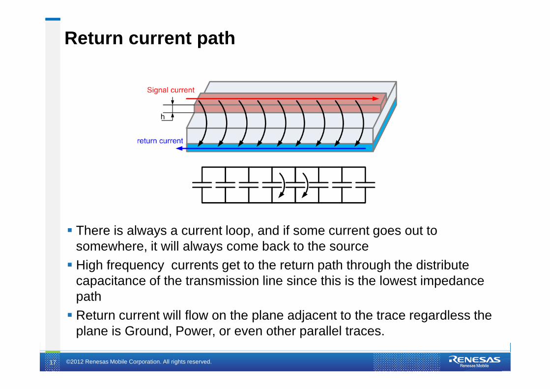
Return current path
There is always a current loop, and if some current goes out to somewhere, it will always come back to the source
High frequency currents get to the return path through the distribute capacitance of the transmission line since this is the lowest impedance path
Return current will flow on the plane adjacent to the trace regardless the plane is Ground, Power, or even other parallel traces.
©2012 Renesas Mobile Corporation. All rights reserved.18
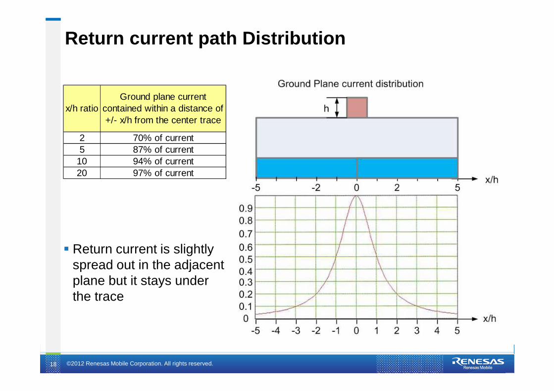
Return current path Distribution
Return current is slightly spread out in the adjacent plane but it stays under the trace
x/h ratioGround plane current
contained within a distance of +/- x/h from the center trace
2 70% of current5 87% of current
10 94% of current20 97% of current

©2012 Renesas Mobile Corporation. All rights reserved.19
High speed signal layer differential pairs
Plan the differential pair routing during the stack-up definition
microstrip stripline

©2012 Renesas Mobile Corporation. All rights reserved.20
Different via technology
For high density routing PCB due to high channel count FPGA and RF, mixed signal and digital signal domain insulation laser via must be used for the best signal integrity performance
Through via
burried via
laser via blind via
©2012 Renesas Mobile Corporation. All rights reserved.21
Outline
PCB stack-up and material losses (εr, tanδ, skin effect)
Signal layers topologies and return current path
Mixed signal design rules
Power and Ground stack-up
Ground routing rules
Signal routing rules
Decoupling strategy: Frequency Domain Target Impedance Method (FDTIM)
Decoupling placement rules
RF/analog ICs
High current power rails

©2012 Renesas Mobile Corporation. All rights reserved.22
Power & Ground layers
Segmented Power planes Power shared as much as possible on any designated power layer to reduce the total layer count
Solid Ground planes Fill the entire layer
Power placed next to a ground Creates planar capacitance
• Aids high frequency decoupling• Reduces electromagnetic Interference (EMI) radiation• Enhance electromagnetic compliance (EMC) robusness
Given a choice between ground plane or power plane as return current path always choose ground plane Using power plane as return current path for high speed routing layers allows switching noise to
couple to the power plane. This must be avoided especially for sensitive power plane such as:• RF and analog transceivers• PLLs• ADCs / DACs
To avoid this situation sensitive power plane must be isolated from signal layers by sandwiching segmented power layers between solid ground layers
©2012 Renesas Mobile Corporation. All rights reserved.23
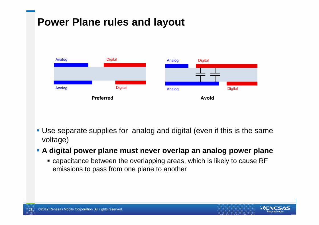
Power Plane rules and layout
Use separate supplies for analog and digital (even if this is the same voltage)
A digital power plane must never overlap an analog power plane capacitance between the overlapping areas, which is likely to cause RF
emissions to pass from one plane to another
©2012 Renesas Mobile Corporation. All rights reserved.24
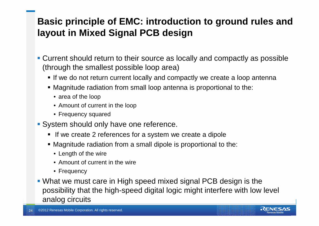
Basic principle of EMC: introduction to ground rule s and layout in Mixed Signal PCB design
Current should return to their source as locally and compactly as possible (through the smallest possible loop area) If we do not return current locally and compactly we create a loop antenna Magnitude radiation from small loop antenna is proportional to the:
• area of the loop• Amount of current in the loop• Frequency squared
System should only have one reference. If we create 2 references for a system we create a dipole Magnitude radiation from a small dipole is proportional to the:
• Length of the wire• Amount of current in the wire• Frequency
What we must care in High speed mixed signal PCB design is the possibility that the high-speed digital logic might interfere with low level analog circuits

©2012 Renesas Mobile Corporation. All rights reserved.25
Separate Analog and Digital grounds ?
Trace crossing over the split between the isolated analog and digital ground plane connected together only at the power supply. High frequency return current have to flow in a large loop producing radiation and high
ground inductance Low levels analog current flowing in a large loop are susceptible to interference Analog ground and digital ground planes are at different RF potentials and connected
together with long wires: this is a very effective dipole
Never ever separate analog and digital grounds when designing a mixed signal PCB

©2012 Renesas Mobile Corporation. All rights reserved.26
Ground rule: use one solid ground plane
Digital ground signal have no desire to flow through the analog portion of the ground plane and corrupt the analog signal
Use one solid ground plane for Mixed PCB design and partition the PCB routing in analog and digital sections
©2012 Renesas Mobile Corporation. All rights reserved.27
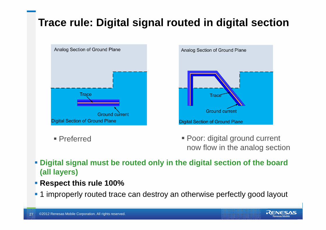
Trace rule: Digital signal routed in digital sectio n
Digital signal must be routed only in the digital s ection of the board (all layers)
Respect this rule 100% 1 improperly routed trace can destroy an otherwise perfectly good layout
Poor: digital ground current now flow in the analog section
Preferred

©2012 Renesas Mobile Corporation. All rights reserved.28
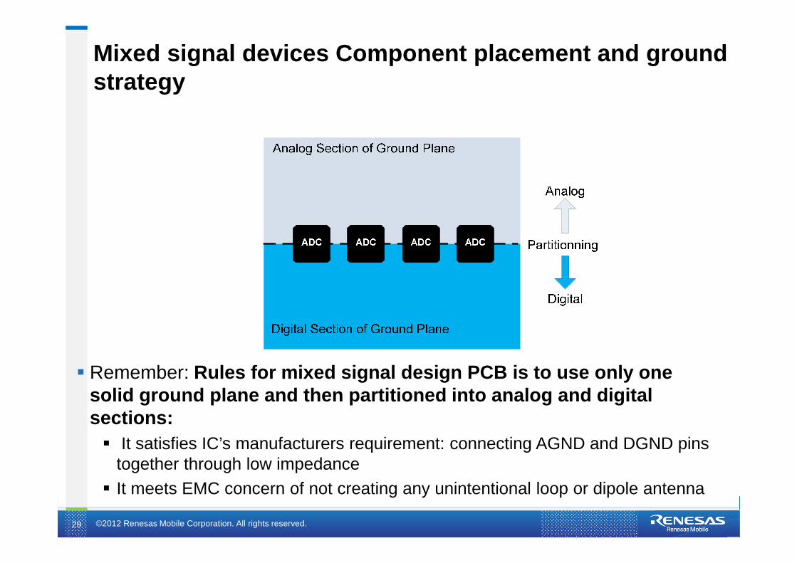
Mixed signal devices Component placement and ground strategy
How to connect ADC analog and digital ground pins ADC manufacturers suggest the following: “The AGND and DGND pins must be connected together externally to the same low impedance ground plane with minimum lead length. Any extra impedance in the DGND connection will couple more digital noise into the analog circuit through the stray capacitance internal to the IC”
©2012 Renesas Mobile Corporation. All rights reserved.29
Mixed signal devices Component placement and ground strategy
Remember: Rules for mixed signal design PCB is to use only on e solid ground plane and then partitioned into analog and digital sections: It satisfies IC’s manufacturers requirement: connecting AGND and DGND pins
together through low impedance It meets EMC concern of not creating any unintentional loop or dipole antenna

©2012 Renesas Mobile Corporation. All rights reserved.30
Summary: Mixed signal PCB partitioning and routing rules
Do not split the ground plane, use one solid planeunder both analog and digital sections of the board Use large area ground planes for low impedance
current return paths Keep over 75% board area for the ground plane Separate analog and digital power planes Use solid ground planes next to power planes Locate all analogue components and lines over the analogue power plane and
all digital components and lines over the digital power plane Do not route traces over the split in the power planes, unless if traces that must
go over the power plane split must be on layers adjacent to the solid ground plane Think about where and how the ground return currents are actually flowing Partition your PCB with separate analog and digital sections Place components properly
Analog Section of Ground Plane
Digital Section of Ground Plane
Analog
Digital
PartitionningADC ADC ADC ADC
©2012 Renesas Mobile Corporation. All rights reserved.31
Outline
PCB stack-up and material losses (εr, tanδ, skin effect)
Signal layers topologies and return current path
Mixed signal design rules
Power and Ground stack-up
Ground routing rules
Signal routing rules
Decoupling strategy: Frequency Domain Target Impedance Method (FDTIM)
Decoupling placement rules
RF/analog Ics
High current power rails
©2012 Renesas Mobile Corporation. All rights reserved.32
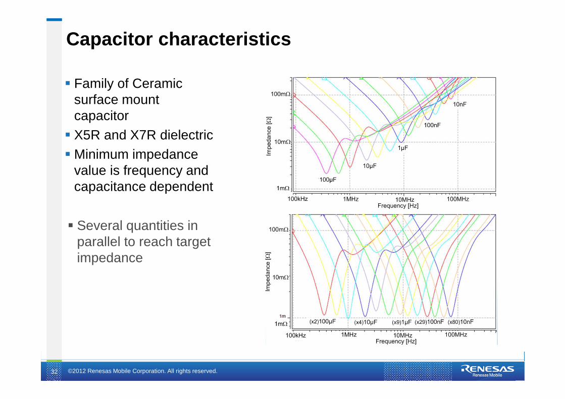
Capacitor characteristics
Family of Ceramic surface mount capacitor
X5R and X7R dielectric Minimum impedance
value is frequency and capacitance dependent
Several quantities in parallel to reach target impedance

©2012 Renesas Mobile Corporation. All rights reserved.33
Target impedance definition
Must Guarantee that supply will not exceed specified tolerance with given transient current
Based on Ohms Law Transient current are important
Ω=−
=−
= m25A1.0A1
02.0Vx1II
xToleranceVZ
MINMAX
DDTARGET

©2012 Renesas Mobile Corporation. All rights reserved.34
System that meet target impedance
Flat in frequency domain Acceptable regulation in time domain
Voltage 1 V
Power 1 W
Max current 1 A 1 ΩTransient current 50 %Min current 0.2 A 5 ΩRipple 2 %Target impedance 25 mΩ
Voltage drop @ Min current, ZTARGET 0.005 V
Voltage drop @ Max current, ZTARGET 0.025 V
0.015 V1.5 %
0.985 V
IR Drop=Voltage drop average, ZTARGET
Voltage average, ZTARGET

©2012 Renesas Mobile Corporation. All rights reserved.35
System with resonant peak
Peak in frequency domain Excessive noise in time domain
Fail to meet ± 2%
Resonant peak must be avoided
©2012 Renesas Mobile Corporation. All rights reserved.36
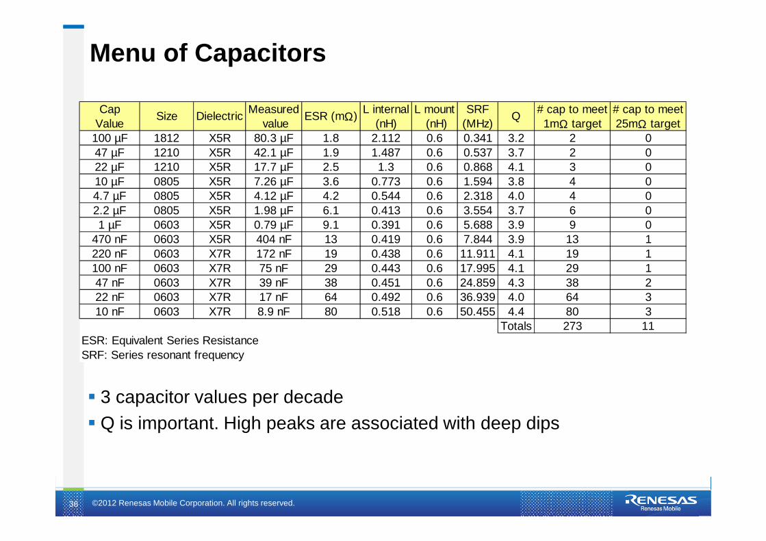
Menu of Capacitors
3 capacitor values per decade Q is important. High peaks are associated with deep dips
CapValue
Size DielectricMeasured
valueESR (mΩ)
L internal(nH)
L mount (nH)
SRF(MHz)
Q# cap to meet
1mΩ target# cap to meet 25mΩ target
100 µF 1812 X5R 80.3 µF 1.8 2.112 0.6 0.341 3.2 2 047 µF 1210 X5R 42.1 µF 1.9 1.487 0.6 0.537 3.7 2 022 µF 1210 X5R 17.7 µF 2.5 1.3 0.6 0.868 4.1 3 010 µF 0805 X5R 7.26 µF 3.6 0.773 0.6 1.594 3.8 4 04.7 µF 0805 X5R 4.12 µF 4.2 0.544 0.6 2.318 4.0 4 02.2 µF 0805 X5R 1.98 µF 6.1 0.413 0.6 3.554 3.7 6 01 µF 0603 X5R 0.79 µF 9.1 0.391 0.6 5.688 3.9 9 0
470 nF 0603 X5R 404 nF 13 0.419 0.6 7.844 3.9 13 1220 nF 0603 X7R 172 nF 19 0.438 0.6 11.911 4.1 19 1100 nF 0603 X7R 75 nF 29 0.443 0.6 17.995 4.1 29 147 nF 0603 X7R 39 nF 38 0.451 0.6 24.859 4.3 38 222 nF 0603 X7R 17 nF 64 0.492 0.6 36.939 4.0 64 310 nF 0603 X7R 8.9 nF 80 0.518 0.6 50.455 4.4 80 3
Totals 273 11ESR: Equivalent Series ResistanceSRF: Series resonant frequency

©2012 Renesas Mobile Corporation. All rights reserved.37
FDTIM
Frequency Domain Target Impedance Method (FDTIM) attributes: Use many different capacitor values
• Perhaps a dozen• 3 values per decade (10, 22, 47)
Usually the least expensive BOM• Standard capacitor (1205, 0805, 0603, 0402 sizes)• Smaller capacitor size
Usually the least board area• Only use large size capacitors where necessary
Uses capacitor that are readily available
CapValue
Size DielectricMeasured
valueESR (mΩ)
L internal(nH)
L mount (nH)
SRF(MHz)
Q# cap to meet 25mΩ target
470 nF 0603 X5R 404 nF 13 0.419 0.6 7.844 3.9 1220 nF 0603 X7R 172 nF 19 0.438 0.6 11.911 4.1 1100 nF 0603 X7R 75 nF 29 0.443 0.6 17.995 4.1 147 nF 0603 X7R 39 nF 38 0.451 0.6 24.859 4.3 222 nF 0603 X7R 17 nF 64 0.492 0.6 36.939 4.0 310 nF 0603 X7R 8.9 nF 80 0.518 0.6 50.455 4.4 3
Totals 11

©2012 Renesas Mobile Corporation. All rights reserved.38
Outline
PCB stack-up and material losses (εr, tanδ, skin effect)
Signal layers topologies and return current path
Mixed signal design rules
Power and Ground stack-up
Ground routing rules
Signal routing rules
Decoupling strategy: Frequency Domain Target Impedance Method (FDTIM)
Decoupling placement rules
RF/analog Ics
High current power rails
©2012 Renesas Mobile Corporation. All rights reserved.39
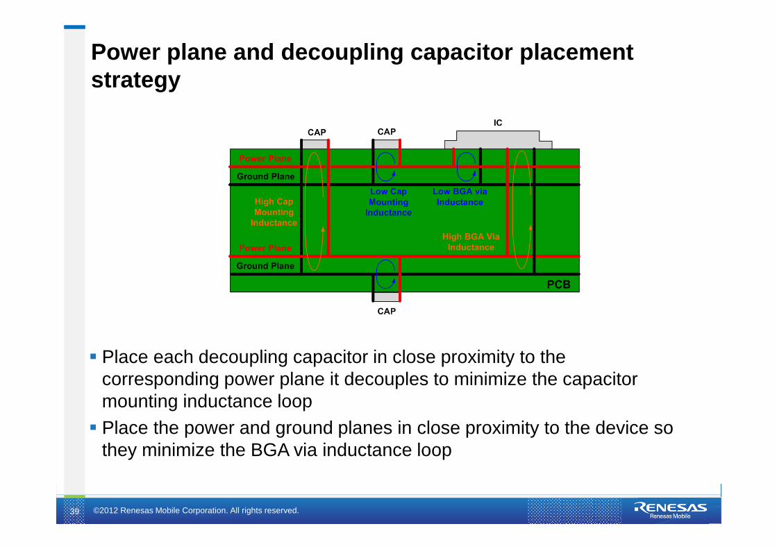
Power plane and decoupling capacitor placement strategy
Place each decoupling capacitor in close proximity to the corresponding power plane it decouples to minimize the capacitor mounting inductance loop
Place the power and ground planes in close proximity to the device so they minimize the BGA via inductance loop

©2012 Renesas Mobile Corporation. All rights reserved.40
Rules for RF, Analog Power plane placement
RF and analog (including PLL and ADC) power rails are susceptible to noise/spurious that can directly impact sensitivity performances.
RF and analog power planes have the highest priority in the power plane stack-up placement over other power rails unless: RF/analog ICs have internal regulation that helps isolate from on-board noise.
Internally regulated power rails can be placed further away from the RF/analog device Current demand of the RF/analog ICs power rails are low enough to yield a high
impedance target that is easily decoupled even when their power planes are placed further away from the IC
General rule: Place RF/analog power rails closest to the RF/analog ICs
©2012 Renesas Mobile Corporation. All rights reserved.41
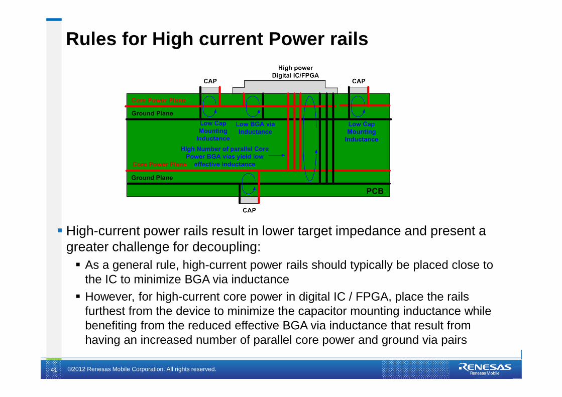
Rules for High current Power rails
High-current power rails result in lower target impedance and present a greater challenge for decoupling: As a general rule, high-current power rails should typically be placed close to
the IC to minimize BGA via inductance However, for high-current core power in digital IC / FPGA, place the rails
furthest from the device to minimize the capacitor mounting inductance while benefiting from the reduced effective BGA via inductance that result from having an increased number of parallel core power and ground via pairs

©2012 Renesas Mobile Corporation. All rights reserved.42
Glossary ADC Analogue to Digital Converter
BGA Ball Grid Array
EMC Electromagnetic conformance
EMI Electromagnetic Interference
ESR Effective Series Resistance
FDTIM
Frequency Domain Target Impedance Method
FPGA Field Programmable Gate Array
GND Ground
IC Integrated Circuit
IOs Inputs/Outputs
PCB Printed Circuit Board
PLL Phase Locked Loop
PWR Power
Q Quality factor
RF Radiofrequency
SI Signal Integrity
SRF Series Resonant Frequency
tan(δ) Loss tangent
δ Skin depth
εr Dielectric constant

©2012 Renesas Mobile Corporation. All rights reserved.43
PCB Stackup Design Considerations for Altera FPGAs, AN-613, Oct. 2010, http://www.altera.com/literature/an/an613.pdf
H.W. Ott, “Partitioning and Layout of a Mixed-Signal PCB”, Printed Circuit Design, June 2001.http://www.hottconsultants.com/pdf_files/june2001pcd_mixedsignal.pdf
Guidelines for Designing High-Speed FPGA PCBs, AN-315, Jul. 2002, http://www.altera.com/literature/an/an315.pdf
L.D. Smith, “Frequency Domain Target Impedance Method for Bypass Capacitor Selection for Power Distribution Systems”, DesignCon2006. http://www.ipblox.com/pubs/DesignCon_2006/DC06_PDN-design_panel-slides.pdf
References

©2012 Renesas Mobile Corporation. All rights reserved.
www.renesasmobile.com


![HMO2024 - SOS · [HMO2024] HMO1522 [HMO1524], Mixed Signal Mixed Signal 2](https://img.pdfslide.us/doc/110x75/606a26e1cd05047284562add/hmo2024-sos-hmo2024-hmo1522-hmo1524-mixed-signal-mixed-signal-2.jpg)