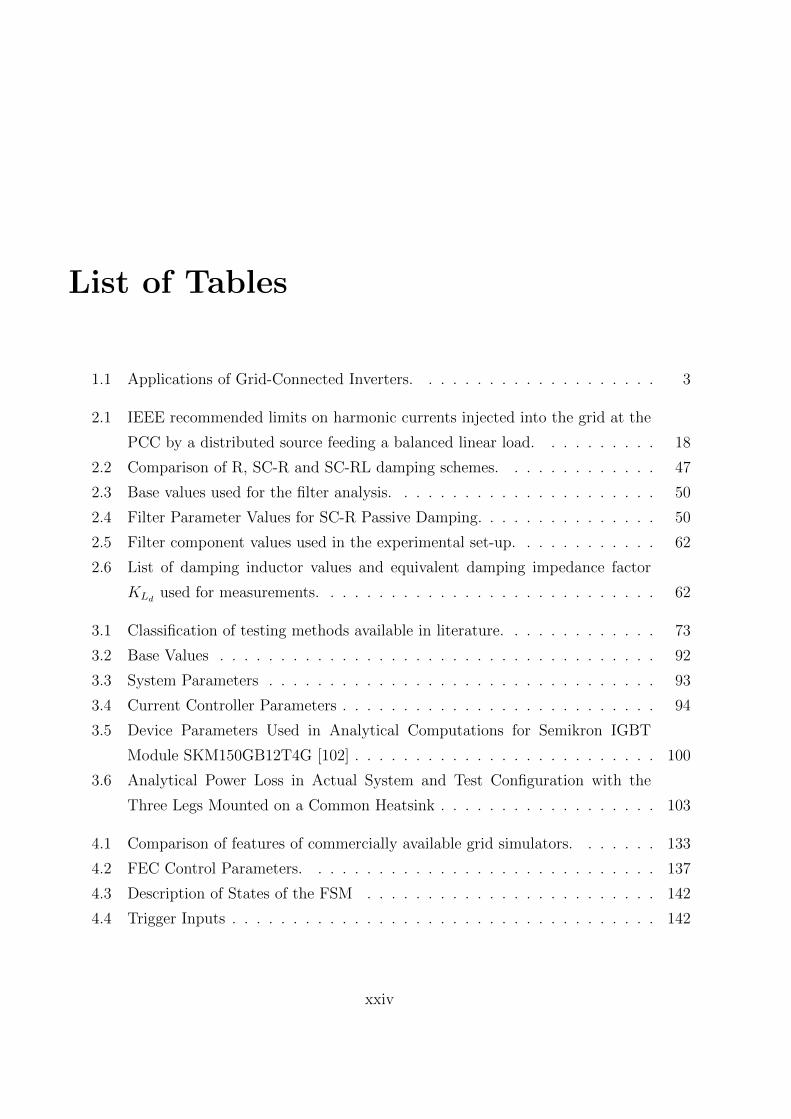
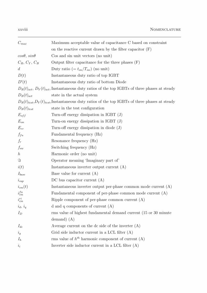
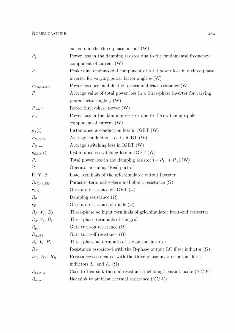
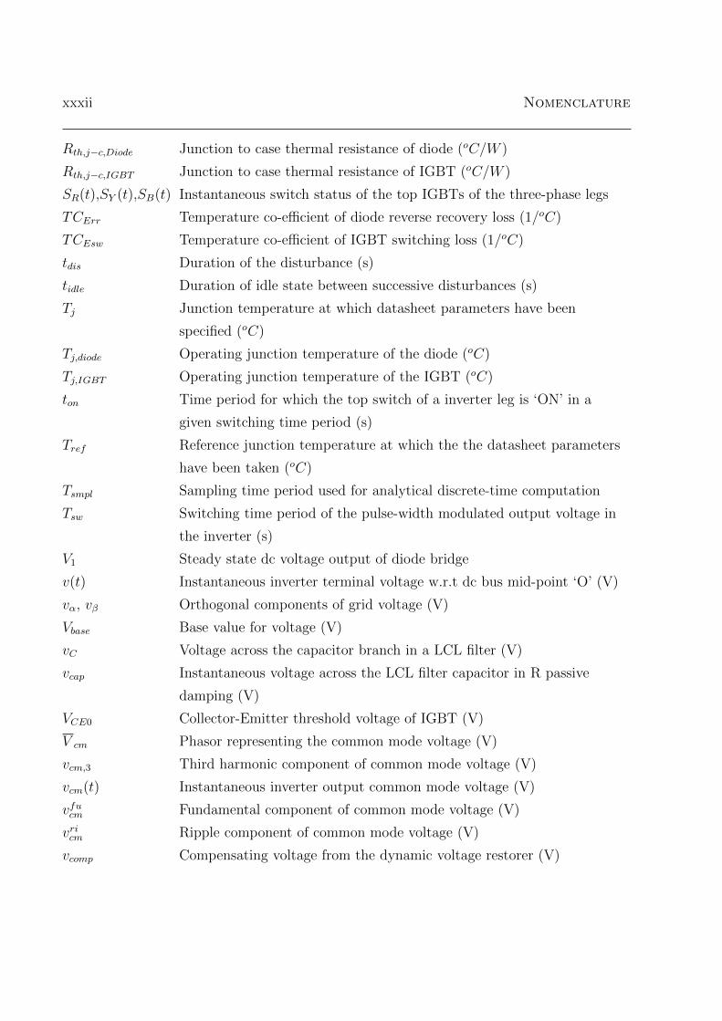
Embed Size (px)
Citation preview
Design and Performance Evaluation of
Sub-Systems of Grid-Connected Inverters
A thesis
submitted for the degree of
Doctor of Philosophy
in the Faculty of Engineering
By
Arun Karuppaswamy B
Department of Electrical Engineering
Indian Institute of Science
Bangalore - 560 012
India
July 2014


To my school teachers...


Acknowledgements
I thank Dr.Vinod John for guiding my Ph.D work. Our technical discussions helped enhance
my knowledge in Power Electronics. His inputs in writing technical manuscripts helped hone
my skill in conveying technical ideas to others in a lucid way. Further, my sincere thanks to
him for allowing me to do the research at my own pace, to have made funds available for
building the hardware and to have provided financial support through project associateship
during the final stages of Ph.D.
I would like to extend my thanks to (Retd.) Prof.V.Ramanarayanan, (Late) Prof.V.T.
Ranganathan and Dr.G.Narayanan for the knowledge they shared with me through the course
work. I would always remember (Retd.)Prof.V.Ramanarayanan for showing the simplicity of
engineering design and for making a better engineer out of me. I would remember the inter-
esting lectures on Electric Drives by (Late)Prof.V.T.Ranganathan. His inputs on practical
issues one would face implementing the theoretical concepts in hardware and the solutions
to the same makes his lectures on Electric Drives unique. I would always be reminded of
the PWM lectures by Dr.G.Narayanan. His lectures threw light on how new concepts can
be taught in a way which makes it simpler for every student to understand.
I thank the IISc administration for making the stay at the institute memorable and com-
fortable. I also thank the Ministry of Human Resource Development (MHRD), Government
of India for their financial support.
I thank all the members associated with the Power Electronics Group, Department of
Electrical Engineering during the period August 2007 to July 2014 for the fruitful discussions
and support. I would like to specifically thank Mr.Srinivas Gulur for helping with parts of
i

ii Acknowledgements
my experimental work. His help speeded up the progress of the experimental work during
the final stages of Ph.D. I also thank all the support staff from the office, workshop, stores,
labs and computer administration of the Department of Electrical Engineering, IISc during
my stay at the institute. Further, I would always remember the Institute Gymkhana and
my association with the sports enthusiasts - especially of Badminton.
Finally, I extend my thanks to my parents, wife, sister, sister’s family and wife’s parents
for their patience, support, encouragement and understanding. Also, my daughter kept up
my spirits with her smiles and acts of innocence during the final stages of my Ph.D. Further,
I thank my friends and relatives for their encouragement and understanding.
Abstract
Grid-connected inverters have wide application in the field of distributed generation and
power quality. As the power level demanded by these applications increase, the design
and performance evaluation of these converters become important. In this thesis, this is
considered from the perspective of power quality, efficiency, thermal performance evaluation,
reliability and control performance evaluation.
The first part of the work focuses on passive damping network design for LCL filters of
grid-connected inverters. Passive damping is considered as it is simple and more reliable.
The work explores a split-capacitor resistive-inductive (SC-RL) passive damping scheme for
use in high power applications. A method for component selection for the SC-RL scheme
that minimises the power loss in the damping resistors while keeping the system well damped
is proposed. Analytical results show the losses and quality factor to be in the range of 0.05-
0.1% and 2.0-2.5 respectively, which are validated experimentally.
In the second part of the work, a test method to evaluate the thermal performance of the
semiconductor devices of a three-phase grid-connected inverter is proposed. Semiconductor
device junction temperatures have to be maintained within datasheet specified limits to avoid
failure in power converters. Thermal time constants can be large and inverters need to be run
for long durations during thermal tests. This consumes a lot of energy and requires sources
and loads that can handle high power. The proposed method eliminates the need for high
power sources and loads. Only energy corresponding to the losses in the test configuration
is consumed. The capability of the method to evaluate the thermal performance of the dc
bus capacitors and the output filter components of the inverter has also been studied. The
method has been experimentally validated for a 4-wire configuration that uses sine-triangle
pulse width modulation and a 3-wire configuration that uses conventional space vector pulse
width modulation.
iii

iv Abstract
In the third part of the work, a test set-up to evaluate the control performance of grid-
connected inverters has been developed. Grid standards require high power grid-connected
inverters to remain connected to the grid under short time grid disturbances like voltage
sags, voltage swells and the like. To test the grid-connected inverter for proper operation
under these disturbances, it is required to re-create them in a controlled manner in the
testing laboratory. A back-to-back connected three-phase inverter has been programmed as
a hardware grid simulator for this purpose. A novel disturbance generation algorithm has
been developed, analysed and implemented in digital controller using finite state machine
model for control of the grid simulator. A wide range of disturbance conditions can be created
using the developed algorithm. Experimental tests have been done on a linear purely resistive
load, a non-linear diode-bridge load and a current-controlled inverter load to validate the
programmed features of the grid simulator.
In the present work, a 50 kVA three-phase back-to-back connected inverter with output
LCL filter is built to study design and performance aspects of subsystems of grid-connected
inverters. The various contributions in the work can be used to improve the reliability and
performance of grid-connected inverters.

Contents
Acknowledgements i
Abstract iii
List of Figures xii
List of Tables xxiv
Acronyms xxv
Nomenclature xxvii
List of Publications xxxv
1 Introduction 1
1.1 Grid-Connected Inverters . . . . . . . . . . . . . . . . . . . . . . . . . . . . . 3
1.1.1 Applications . . . . . . . . . . . . . . . . . . . . . . . . . . . . . . . . 4
1.1.1.1 Power Quality Applications . . . . . . . . . . . . . . . . . . 4
1.1.1.2 Distributed Generation Applications . . . . . . . . . . . . . 6
1.1.1.3 Front End Conversion (FEC) Applications . . . . . . . . . . 6
1.2 Research in the Area of Grid-Connected Inverters: An Overview . . . . . . . 8
1.2.1 Design Aspects . . . . . . . . . . . . . . . . . . . . . . . . . . . . . . 8
1.2.1.1 Topology . . . . . . . . . . . . . . . . . . . . . . . . . . . . 8
1.2.1.2 DC Bus Capacitor Selection . . . . . . . . . . . . . . . . . . 9
1.2.1.3 Busbar and Snubber Design . . . . . . . . . . . . . . . . . . 9
1.2.1.4 Output Filter Design . . . . . . . . . . . . . . . . . . . . . . 10
v

vi Contents
1.2.1.5 Output Filter Damping . . . . . . . . . . . . . . . . . . . . 10
1.2.1.6 Electro-Magnetic Interference (EMI) Filter Design . . . . . 10
1.2.1.7 Thermal Design . . . . . . . . . . . . . . . . . . . . . . . . . 10
1.2.2 Control Aspects . . . . . . . . . . . . . . . . . . . . . . . . . . . . . . 11
1.2.2.1 Modulation Techniques . . . . . . . . . . . . . . . . . . . . 11
1.2.2.2 Phase Locked Loops . . . . . . . . . . . . . . . . . . . . . . 11
1.2.2.3 Current Control . . . . . . . . . . . . . . . . . . . . . . . . 11
1.2.2.4 Voltage Control . . . . . . . . . . . . . . . . . . . . . . . . . 12
1.2.3 Grid Connection Standards . . . . . . . . . . . . . . . . . . . . . . . 12
1.3 Scope of the Thesis . . . . . . . . . . . . . . . . . . . . . . . . . . . . . . . . 12
1.4 Experimental Set-up . . . . . . . . . . . . . . . . . . . . . . . . . . . . . . . 13
1.5 Organisation of the Thesis . . . . . . . . . . . . . . . . . . . . . . . . . . . . 14
1.6 Summary . . . . . . . . . . . . . . . . . . . . . . . . . . . . . . . . . . . . . 15
2 LCL Filter Design 17
2.1 Regulations on Power Sources Connected to the Grid . . . . . . . . . . . . . 18
2.1.1 Need for LCL Filter in Grid-Connected Inverters . . . . . . . . . . . 19
2.2 LCL Filter Design . . . . . . . . . . . . . . . . . . . . . . . . . . . . . . . . . 20
2.2.1 Choice of L . . . . . . . . . . . . . . . . . . . . . . . . . . . . . . . . 21
2.2.2 Choice of L1 and L2 . . . . . . . . . . . . . . . . . . . . . . . . . . . 24
2.2.3 Selection of C . . . . . . . . . . . . . . . . . . . . . . . . . . . . . . . 26
2.3 Resonance in LCL Filters . . . . . . . . . . . . . . . . . . . . . . . . . . . . 26
2.3.1 Parallel Resonance . . . . . . . . . . . . . . . . . . . . . . . . . . . . 26
2.3.2 Series Resonance . . . . . . . . . . . . . . . . . . . . . . . . . . . . . 27
2.4 Damping Design for LCL Filter . . . . . . . . . . . . . . . . . . . . . . . . . 28
2.4.1 Passive Damping Schemes . . . . . . . . . . . . . . . . . . . . . . . . 28
2.4.1.1 Purely Resistive (R) Damping Scheme . . . . . . . . . . . . 28
2.4.1.2 Split-Capacitor Resistive (SC-R) Damping Scheme . . . . . 30
2.4.1.3 Split-Capacitor Resistive-Inductive (SC-RL) Damping Scheme 30
2.4.1.4 Focus of Work . . . . . . . . . . . . . . . . . . . . . . . . . 30
2.4.2 Modelling and Analysis of SC-RL Damped LCL Filter . . . . . . . . 31
2.4.2.1 Modelling of SC-RL Damped LCL Filter . . . . . . . . . . . 31
2.4.2.2 Quality Factor (QF) . . . . . . . . . . . . . . . . . . . . . . 34

Contents vii
2.4.2.3 Power Loss . . . . . . . . . . . . . . . . . . . . . . . . . . . 37
2.4.2.4 Computation of iRd,rms . . . . . . . . . . . . . . . . . . . . . 38
2.4.3 Comparison of Damping Schemes . . . . . . . . . . . . . . . . . . . . 46
2.4.4 SC-RL Damping Circuit Design . . . . . . . . . . . . . . . . . . . . . 48
2.4.4.1 Selection of Ideal LCL Filter Components: Choice of Reso-
nance Frequency, ωr . . . . . . . . . . . . . . . . . . . . . . 48
2.4.4.2 Selection of Components for SC-R Damping Scheme . . . . 49
2.4.4.3 Selection of Ld for SC-RL Damping Scheme . . . . . . . . . 54
2.4.4.4 Damping Impedance Factor (KLd) - Physical Implication and
Some Observations . . . . . . . . . . . . . . . . . . . . . . . 54
2.4.5 Summary of Component Selection Procedure for an SC-RL Damped
LCL Filter . . . . . . . . . . . . . . . . . . . . . . . . . . . . . . . . . 61
2.4.6 Experimental Results . . . . . . . . . . . . . . . . . . . . . . . . . . . 62
2.4.6.1 Measurement of QF . . . . . . . . . . . . . . . . . . . . . . 63
2.4.6.2 Measurement of Power Loss (Pfu and Pri) . . . . . . . . . . 63
2.4.6.3 Filtering Performance . . . . . . . . . . . . . . . . . . . . . 65
2.5 Summary . . . . . . . . . . . . . . . . . . . . . . . . . . . . . . . . . . . . . 68
3 Thermal Performance Evaluation of High Power Grid-Connected Inverters 71
3.1 Inverter Testing Methods - A Survey . . . . . . . . . . . . . . . . . . . . . . 72
3.1.1 Regenerative Method . . . . . . . . . . . . . . . . . . . . . . . . . . . 73
3.1.2 Opposition Method . . . . . . . . . . . . . . . . . . . . . . . . . . . . 75
3.1.3 Focus of Work . . . . . . . . . . . . . . . . . . . . . . . . . . . . . . . 76
3.2 Proposed Test Method . . . . . . . . . . . . . . . . . . . . . . . . . . . . . . 77
3.2.1 Actual System and Test Configuration . . . . . . . . . . . . . . . . . 77
3.2.2 Test Method . . . . . . . . . . . . . . . . . . . . . . . . . . . . . . . . 79
3.2.3 Choice of Current References . . . . . . . . . . . . . . . . . . . . . . 80
3.3 Phasor Analysis . . . . . . . . . . . . . . . . . . . . . . . . . . . . . . . . . . 81
3.3.1 Operation of the Actual System and Test Configuration – A Physical
Insight . . . . . . . . . . . . . . . . . . . . . . . . . . . . . . . . . . . 83
3.4 Common Mode and Differential Mode Equivalent Circuits . . . . . . . . . . 84
3.4.1 Common Mode and Differential Mode Voltages and Currents - Defined 86
3.4.2 Equivalent Circuits of the Actual System . . . . . . . . . . . . . . . . 86

viii Contents
3.4.2.1 For Low Fundamental Frequency Component . . . . . . . . 87
3.4.2.2 For High Frequency Switching Ripple Components . . . . . 87
3.4.3 Equivalent Circuits of the Proposed Test Configuration . . . . . . . . 87
3.4.3.1 For Low Fundamental Frequency Component . . . . . . . . 87
3.4.3.2 For High Frequency Switching Ripple Components . . . . . 88
3.5 Current Control for the Proposed Test Configuration . . . . . . . . . . . . . 88
3.6 Base Values, System Parameters and Control Parameters . . . . . . . . . . . 90
3.7 Analysis of Low Frequency Voltage Ripple in DC Bus Capacitor . . . . . . . 92
3.7.1 Low Frequency Ripple due to Output Fundamental CM Component . 94
3.7.2 Low Frequency Ripple due to Output Fundamental DM Component . 95
3.8 Analysis and Experimental Results – 4-Wire Configuration . . . . . . . . . . 96
3.8.1 Current Control . . . . . . . . . . . . . . . . . . . . . . . . . . . . . . 96
3.8.2 Thermal Testing of Semiconductor Devices . . . . . . . . . . . . . . . 96
3.8.2.1 Heatsink Temperature . . . . . . . . . . . . . . . . . . . . . 97
3.8.2.2 Power Loss in Individual Semiconductor Devices . . . . . . 105
3.8.2.3 Input Power . . . . . . . . . . . . . . . . . . . . . . . . . . . 105
3.8.3 Testing of DC Bus Capacitors . . . . . . . . . . . . . . . . . . . . . . 106
3.8.3.1 Instantaneous Switch States . . . . . . . . . . . . . . . . . . 107
3.8.3.2 Instantaneous Output Grid-Side Inductor Currents . . . . . 112
3.8.4 Testing of Output Filter Components . . . . . . . . . . . . . . . . . . 113
3.8.4.1 Fundamental Frequency Currents in the Output Filter Com-
ponents . . . . . . . . . . . . . . . . . . . . . . . . . . . . . 114
3.8.4.2 Ripple Currents in the Output Filter Components . . . . . . 114
3.9 Analysis and Experimental Results – 3-Wire Configuration . . . . . . . . . . 116
3.9.1 Current Control . . . . . . . . . . . . . . . . . . . . . . . . . . . . . . 117
3.9.1.1 Effect of Third Harmonic Common Mode on Voltage References120
3.9.2 Thermal Testing of Semiconductor Devices . . . . . . . . . . . . . . . 123
3.9.3 Testing of DC Bus Capacitors . . . . . . . . . . . . . . . . . . . . . . 125
3.9.4 Testing of Output Filter Components . . . . . . . . . . . . . . . . . . 126
3.10 Summary . . . . . . . . . . . . . . . . . . . . . . . . . . . . . . . . . . . . . 126
4 Control Performance Evaluation of Grid-Connected Inverters 129
4.1 Grid Simulators - A Survey . . . . . . . . . . . . . . . . . . . . . . . . . . . 130
Contents ix
4.1.1 Grid Simulation Methods Available in Literature . . . . . . . . . . . 130
4.1.2 Commercially Available Grid Simulators . . . . . . . . . . . . . . . . 132
4.1.3 Focus of Work . . . . . . . . . . . . . . . . . . . . . . . . . . . . . . . 132
4.2 Grid Simulator Topology . . . . . . . . . . . . . . . . . . . . . . . . . . . . . 135
4.3 Grid Simulator Controls . . . . . . . . . . . . . . . . . . . . . . . . . . . . . 135
4.3.1 Front-End Converter Control . . . . . . . . . . . . . . . . . . . . . . 135
4.3.2 Output Inverter Control . . . . . . . . . . . . . . . . . . . . . . . . . 137
4.4 Grid Simulator Operation . . . . . . . . . . . . . . . . . . . . . . . . . . . . 137
4.4.1 Start-Up Sequence of Grid Simulator . . . . . . . . . . . . . . . . . . 138
4.4.2 Modes during Disturbance Generation . . . . . . . . . . . . . . . . . 138
4.5 Voltage Disturbance Generation Algorithm . . . . . . . . . . . . . . . . . . . 141
4.6 Grid Simulator Parameters and Test Loads . . . . . . . . . . . . . . . . . . . 143
4.7 Experimental Results . . . . . . . . . . . . . . . . . . . . . . . . . . . . . . . 145
4.7.1 Modes of Operation of Grid Simulator . . . . . . . . . . . . . . . . . 145
4.7.2 Sag, Swell and Frequency Deviation . . . . . . . . . . . . . . . . . . . 145
4.7.3 Load Testing . . . . . . . . . . . . . . . . . . . . . . . . . . . . . . . 145
4.7.3.1 Linear Purely Resistive Load . . . . . . . . . . . . . . . . . 145
4.7.3.2 Non-Linear Diode-Bridge Load . . . . . . . . . . . . . . . . 145
4.7.3.3 Current Controlled Inverter Load . . . . . . . . . . . . . . . 149
4.8 Future Scope of Work . . . . . . . . . . . . . . . . . . . . . . . . . . . . . . . 151
4.9 Summary . . . . . . . . . . . . . . . . . . . . . . . . . . . . . . . . . . . . . 156
5 Conclusion 157
5.1 LCL Filter Damping Design . . . . . . . . . . . . . . . . . . . . . . . . . . . 157
5.2 Thermal Testing . . . . . . . . . . . . . . . . . . . . . . . . . . . . . . . . . 158
5.3 Grid Simulator . . . . . . . . . . . . . . . . . . . . . . . . . . . . . . . . . . 159
5.4 Future Scope of Work . . . . . . . . . . . . . . . . . . . . . . . . . . . . . . . 159
5.5 Summary . . . . . . . . . . . . . . . . . . . . . . . . . . . . . . . . . . . . . 160
Appendix A Details of Experimental Set-Up 161
Appendix B Harmonic Limits: Terminology, Definitions and Test Method 163
B.1 Point of Common Coupling (PCC) . . . . . . . . . . . . . . . . . . . . . . . 163
B.2 Harmonic Measures . . . . . . . . . . . . . . . . . . . . . . . . . . . . . . . . 164

x Contents
B.2.1 Total Harmonic Distortion (THD) . . . . . . . . . . . . . . . . . . . . 165
B.2.2 Total Demand Distortion (TDD) . . . . . . . . . . . . . . . . . . . . 165
B.2.3 Total Rated current Distortion (TRD) . . . . . . . . . . . . . . . . . 166
B.3 Design Test for Conformance to Harmonic Standards . . . . . . . . . . . . . 167
Appendix C Quality factor in the context of LCL filter design 169
C.1 Quality factor in second-order series RLC circuits . . . . . . . . . . . . . . . 169
C.1.1 Important observations on QF . . . . . . . . . . . . . . . . . . . . . . 171
C.2 Quality factor in higher order systems . . . . . . . . . . . . . . . . . . . . . . 172
C.2.1 Application in LCL filter design . . . . . . . . . . . . . . . . . . . . . 172
Appendix D Quality Factor and Power Loss Expressions 173
D.1 State Space Model . . . . . . . . . . . . . . . . . . . . . . . . . . . . . . . . 173
D.1.1 R Passive Damping . . . . . . . . . . . . . . . . . . . . . . . . . . . . 173
D.1.2 SC-R Passive Damping . . . . . . . . . . . . . . . . . . . . . . . . . . 174
D.2 Quality Factor . . . . . . . . . . . . . . . . . . . . . . . . . . . . . . . . . . . 175
D.2.1 R Passive Damping . . . . . . . . . . . . . . . . . . . . . . . . . . . . 175
D.2.2 SC-R Passive Damping . . . . . . . . . . . . . . . . . . . . . . . . . . 176
D.3 Power Loss . . . . . . . . . . . . . . . . . . . . . . . . . . . . . . . . . . . . 176
D.3.1 R Passive Damping . . . . . . . . . . . . . . . . . . . . . . . . . . . . 176
D.3.2 SC-R Passive Damping . . . . . . . . . . . . . . . . . . . . . . . . . . 177
Appendix E Computation of Semiconductor Power Losses in Inverter 179
E.1 Conduction Loss . . . . . . . . . . . . . . . . . . . . . . . . . . . . . . . . . 180
E.1.1 IGBT Conduction Loss . . . . . . . . . . . . . . . . . . . . . . . . . . 180
E.1.2 Diode Conduction Loss . . . . . . . . . . . . . . . . . . . . . . . . . . 181
E.1.3 IGBT and Diode Conduction Losses in CSVPWM . . . . . . . . . . . 182
E.2 Switching Loss . . . . . . . . . . . . . . . . . . . . . . . . . . . . . . . . . . 182
E.2.1 IGBT Turn-on and Turn-off Losses . . . . . . . . . . . . . . . . . . . 182
E.2.2 Diode Reverse Recovery Loss . . . . . . . . . . . . . . . . . . . . . . 183
E.3 Module Terminal Loss . . . . . . . . . . . . . . . . . . . . . . . . . . . . . . 184
References 185

List of Figures
1.1 Grid-connected inverter. Solid lines indicate a 3-wire configuration and dashed
lines indicate a 4-wire configuration. Control inputs depend on the application. 2
1.2 A STATCOM providing reactive power support to the load. The losses in
transmitting the reactive current from the grid to the load terminal is reduced.
The power factor is near unity for the fundamental frequency current drawn
from the grid. . . . . . . . . . . . . . . . . . . . . . . . . . . . . . . . . . . . 5
1.3 An active power filter providing reactive and harmonic current support to
the load. The active power filter has the same topology as a STATCOM.
The difference lies mainly in the control. The active power filter compensates
for the fundamental frequency reactive current and the harmonic frequency
current requirements of the load. . . . . . . . . . . . . . . . . . . . . . . . . 5
1.4 A dynamic voltage restorer (DVR) to maintain quality voltage (vload) at the
load terminal. The DVR compensates for the deviations in the grid voltage
(vg) by injecting a compensating voltage ‘vcomp’ in series with the grid voltage
through a series injection transformer. . . . . . . . . . . . . . . . . . . . . . 7
1.5 An unified power quality conditioner (UPQC). The UPQC unifies the capa-
bilities of a APF and a DVR. Besides ensuring a sinusoidal near unity power
factor current to be drawn from the grid, it maintains quality voltage at the
load terminals. . . . . . . . . . . . . . . . . . . . . . . . . . . . . . . . . . . 7
2.1 Harmonic spectrum of terminal voltage measured with respect to dc bus mid-
point in a 3-phase 2-level inverter for a fundamental output voltage of 240
V and dc bus voltage of 800 V. The spectrum is valid for the case when the
inverter just balances the grid. Switching frequency fsw considered is 10kHz. 19
xii
List of Figures xiii
2.2 3-phase 2-level inverter connected to the grid through a LCL filter in a 3-wire
configuration (solid lines) and 4-wire configuration (dashed lines). . . . . . . 21
2.3 Per-phase circuit equivalent of the LCL filter connected between a 3-phase
2-level inverter and the grid in a 4-wire configuration. The grid impedance is
lumped along with L2. . . . . . . . . . . . . . . . . . . . . . . . . . . . . . . 22
2.4 A typical bode plot of the transfer functionIg(s)
Vi(s)for an ideal LCL filter. The
pass band and stop band frequencies are decided by the chosen resonance
frequency. All frequencies above the resonance frequency are attenuated. . . 23
2.5 Harmonic spectrum of terminal voltage measured with respect to dc bus mid-
point in a 3-phase 2-level inverter for a fundamental output voltage of 240
V and dc bus voltage of 800 V. The spectrum is valid for the case when the
inverter just balances the grid. Switching frequency fsw considered is 9.75kHz. 25
2.6 Passive damping schemes. (a) Purely Resistive (R) damping scheme. (b)
Split-Capacitor Resistive (SC-R) damping scheme. (c) Split-Capacitor Resistive-
Inductive (SC-RL) passive damping scheme. . . . . . . . . . . . . . . . . . . 29
2.7 Conceptual view of SC-RL damping scheme showing the predominant current
flow paths in the filter capacitor branch at different frequencies. . . . . . . . 30
2.8 An SC-RL damped LCL filter at the output of one phase of a three-phase
4-wire inverter, showing the various state variables used to model the system. 32
2.9 A typical bode plot of the transfer function VC(s)Vi(s)
for a SC-RL damped LCL
filter. The quality factor is a measure of the resonance peak of the plot with
respect to the flat portion of the curve extending from dc to near resonance
frequency. . . . . . . . . . . . . . . . . . . . . . . . . . . . . . . . . . . . . . 35
2.10 Variation of rms value of ripple component of iRdwith duty ratio for Ld =
500µH. The rms ripple current for a sine output voltage is also shown for the
3-phase 3-wire and 3-phase 4-wire cases. . . . . . . . . . . . . . . . . . . . . 45
2.11 Variation of minimum QF with aC = Cd/C1 including the effect of resonance
frequency shift. The plot uses ωr =√ωfu · ωsw, rated 3-phase power (power
base) of 250 kVA for the inverter and nominal grid voltage (voltage base,
frequency base) = 240 V, 50 Hz. The minimum quality factor curve does not
change with switching frequency. . . . . . . . . . . . . . . . . . . . . . . . . 51

xiv List of Figures
2.12 Variation of PT with aC = Cd/C1 for varying values of switching frequency.
The plot uses ωr =√ωfu · ωsw, inverter rated 3-phase power (power base) =
250 kVA and nominal grid voltage (voltage base, frequency base) = 240 V, 50
Hz. . . . . . . . . . . . . . . . . . . . . . . . . . . . . . . . . . . . . . . . . . 52
2.13 Pole-Zero plot of SC-R damped LCL filter for varying Rd. Rd is varied from
0.5√L/C to 10
√L/C. The system has maximum damping when Rd is around√
L/C. The dashed arrows indicate pole movement for increasing Rd. The
solid arrows indicate poles and zeros for the component selection C1 = Cd and
Rd =√L/C. . . . . . . . . . . . . . . . . . . . . . . . . . . . . . . . . . . . 53
2.14 Variation of different components of power loss in the damping resistors versus
damping impedance factor KLd. . . . . . . . . . . . . . . . . . . . . . . . . . 55
2.15 QF determined numerically from the magnitude bode plot versus damping
impedance factor KLdincluding the effect of resonance frequency shift. . . . 56
2.16 Variation of QF with KLdincluding the effect of resonance frequency shift
for varying values of switching frequency. The plot uses ωr =√ωfu · ωsw,
inverter rated 3-phase power (power base) = 250 kVA and nominal grid voltage
(voltage base, frequency base) = 240 V, 50 Hz. . . . . . . . . . . . . . . . . . 58
2.17 Variation of PT with KLdfor varying values of switching frequency. The plot
uses ωr =√ωfu · ωsw, inverter rated 3-phase power (power base) = 250 kVA
and nominal grid voltage (voltage base, frequency base) = 240 V, 50 Hz. . . 59
2.18 Pole-Zero plot of SC-RL damped LCL filter for varying KLd. KLd
is varied
from 0.5×[
1
2· ωrωfu
]to 10×
[1
2· ωrωfu
].The system has maximum damping
whenKLdis
1
2· ωrωfu
. The dashed arrows indicate pole movement for increasing
KLd. The solid arrows indicate poles and zeros for KLd
=1
2· ωrωfu
. . . . . . . 60
2.19 Theoretical and experimental quality factor curves as a function of the damp-
ing impedance factor KLd. . . . . . . . . . . . . . . . . . . . . . . . . . . . . 63
2.20 Theoretical and experimental power loss comparison as a function of the
damping impedance factor KLd. Curves for the fundamental loss component,
switching loss component and total loss are indicated. . . . . . . . . . . . . . 64

List of Figures xv
2.21 Operation of the inverter with LCL filter at an output of 100 V (rms), 40 A
(rms) at unity power factor. Ch1: Inverter-side inductor current (100 A/div);
Ch2: Grid-side inductor current (100 A/div); Ch3: voltage across capacitor
Vc (100 V/div). . . . . . . . . . . . . . . . . . . . . . . . . . . . . . . . . . . 65
2.22 Power converter waveforms and spectrum at an output of 100 V (rms), 40 A
(rms) and unity power factor at the inverter output terminal without the SC-
RL passive damping circuitry. (a) Operation of the inverter with undamped
LCL filter. Ch1: Grid-side inductor current (100 A/div); Ch2: Inverter-side
inductor current (100 A/div); Ch4: voltage across capacitor Vc (100 V/div).
(b) Spectrum of waveforms in (a). . . . . . . . . . . . . . . . . . . . . . . . . 66
2.23 Power converter waveforms and spectrum at an output of 100 V (rms), 40 A
(rms) and unity power factor at the inverter output terminal with the SC-
RL passive damping circuitry. (a) Operation of the inverter with damped
LCL filter. Ch1: Grid-side inductor current (100 A/div); Ch2: Inverter-side
inductor current (100 A/div); Ch4: voltage across capacitor Vc (100 V/div).
(b) Spectrum of waveforms in (a). . . . . . . . . . . . . . . . . . . . . . . . . 67
3.1 Regenerative and opposition test methods. (a) Regenerative configuration for
inverter testing where either an ac source or a dc source shown in dashed lines
will supply the losses in the system. (b) Regenerative configuration for UPS
testing where only an ac source can be used for supplying the losses as both
the input and output of the UPS are ac. (c) Opposition method for testing
an inverter. The three legs of the inverter are tested one at a time. . . . . . 74
3.2 Actual system and test configurations. Solid lines indicate a 3-wire system
and dashed lines indicate a 4-wire system. (a) Actual system consisting of
a generic three-phase grid-connected inverter with output LCL filter. (b)
Proposed test configuration consisting of a three-phase inverter with output
LCL filter shorted. R-phase leg is considered to be the Leg Under Test (LUT).
A low power ac-dc converter feeds the losses at UPF. . . . . . . . . . . . . . 78
3.3 Alternative test configuration consisting of a three-phase inverter with output
LCL filter synchronized to a single-phase grid. This configuration is applicable
only to 4-wire systems. . . . . . . . . . . . . . . . . . . . . . . . . . . . . . . 79
xvi List of Figures
3.4 Equivalent circuit of test configuration under proposed method of operation.
LR1, LY 1 and LB1 represent the inverter-side output inductors of the three
phases, LR2, LY 2 and LB2 represent the grid-side output inductors of the three
phases and CR, CY and CB represent the output filter capacitors of the three
phases. . . . . . . . . . . . . . . . . . . . . . . . . . . . . . . . . . . . . . . . 80
3.5 Phasor representations corresponding to the fundamental frequency when R-
phase is the LUT. (a) For the actual system. (b) For the proposed test config-
uration. The phasor diagram has been drawn for a lagging grid power factor
angle of 30o. The small fundamental frequency current through the output
filter capacitors has been neglected in drawing this phasor diagram. . . . . . 82
3.6 Per-phase common mode and differential mode equivalent circuits of the in-
verter output filter for a three-phase 4-wire configuration. (a) For the actual
system. (b) For the proposed test configuration. R-phase has been used as a
representative phase. The circuits are applicable for the other phases also. . 85
3.7 Differential mode equivalent circuit for controller design of test configuration.
LR = LR1 + LR2; LY = LY 1 + LY 2; LB = LB1 + LB2. RR, RY , RB are the
resistances associated with LR, LY and LB respectively. . . . . . . . . . . . . 88
3.8 Block diagram for current control shown for Y phase. The current control is
implemented for two phases of the inverter. . . . . . . . . . . . . . . . . . . . 91
3.9 Complete control block diagram for the test configuration. R-phase is assumed
to be the LUT. vRiO is an open loop voltage. vRiO is set to be the same as
the voltage at the R-phase output terminal of the inverter in the actual system. 91
3.10 Three phase currents CH1: iR, CH2: iY , CH3: iB and R-phase LCL filter
capacitor voltage CH4: vC in the test configuration while emulating a grid-
connected inverter that injects (a) a 90o lagging current (b) an in-phase current
(c) a 90o leading current (d) an 180o out-of-phase current at the point of
common coupling with the grid. Experimental parameters are as shown in
Table. 3.3. CH1, CH2, CH3: 50A/div; CH4: 100V/div. . . . . . . . . . . . . 97

List of Figures xvii
3.11 Thermal model of the three-phase inverter shown in Fig. 3.2. The detailed
model of one leg is shown. The blocks ‘Y Phase Leg’ and ‘B Phase Leg’ also
have the same thermal model as the R-phase leg. Rth,h−a, Rth,c−h, Rth,j−c,IGBT ,
Rth,j−c,Diode are the thermal resistances of heatsink, case to heatsink including
heatsink paste, IGBT junction to case and Diode junction to case respectively.
PS1, PD1, PS2 and PD2 are the average power loss in the devices S1, D1, S2
and D2 shown in Fig. 3.2. . . . . . . . . . . . . . . . . . . . . . . . . . . . . 98
3.12 Analytical power loss curves for varying grid power factor angle, φ. (a) Power
loss in actual system shown in Fig. 3.2(a). The power loss components in one
leg has been shown. The power loss curves are the same for all the legs. (b) A
magnified view of the total power loss encircled in dashed lines in Fig. 3.12(a). 101
3.13 Analytical power loss curves in test configuration shown in Fig. 3.2(b) for the
phases R,Y and B. The power loss has been shown for varying grid power
factor angle, φ. . . . . . . . . . . . . . . . . . . . . . . . . . . . . . . . . . . 102
3.14 Plot of analytical and experimental heatsink temperature rise over ambient
for varying φ with the three legs of the inverter mounted on the same heatsink
and modulated using sine-triangle PWM. . . . . . . . . . . . . . . . . . . . . 104
3.15 Three-phase inverter voltages (vRi, vYi and vBi
) and three-phase grid-side
inductor currents (iR, iY and iB) for a lagging grid power factor angle of 30o.
(a) In the actual system. (b) In the test configuration. . . . . . . . . . . . . 108
3.16 Switching cycle at the 60o line shown in Fig. 3.15. The switching states SR, SY
and SB during the different intervals are indicated in the format (SR, SY , SB).
(a) For actual system. (b). For test configuration. . . . . . . . . . . . . . . . 109
3.17 Analytical dc bus rms current of the actual system for varying grid power
factor angles at a dc bus voltage of 800 V, analytical dc bus rms current
of the test configuration for a lagging inverter power factor angle of 90o at
a dc bus voltage of 800 V and experimental dc bus rms current of the test
configuration for a lagging inverter power factor angle of near 90o at a reduced
dc bus voltage of 60 V. . . . . . . . . . . . . . . . . . . . . . . . . . . . . . . 112
3.18 Analytical and experimental rms ripple currents in the output filter capacitors
of the three legs in the test configuration at rated operating conditions. R-
phase is the LUT. . . . . . . . . . . . . . . . . . . . . . . . . . . . . . . . . . 115
xviii List of Figures
3.19 Three-phase sinusoidal modulating signals and the common mode required to
generate the references in the case of CSVPWM. The common mode signal
can be approximated using a triangular waveform of peak equal to one-fourth
of the peak of the sine waveform. Further, the triangular waveform can itself
be approximated using its fundamental frequency component as shown. . . . 117
3.20 Modulating signals for CSVPWM. The actual and the approximated wave-
forms using the common mode approximation shown in Fig. 3.19 have been
shown. . . . . . . . . . . . . . . . . . . . . . . . . . . . . . . . . . . . . . . . 118
3.21 Three phase currents CH1: iR, CH2: iY , CH3: iB and R-phase LCL filter
capacitor voltage CH4: vC in the test configuration while emulating a grid-
connected inverter in a 3-wire configuration that injects (a) a 90o lagging
current (b) an in-phase current (c) a 90o leading current (d) an 180o out-of-
phase current at the point of common coupling with the grid. Experimental
parameters are as shown in Table. 3.3. CH1, CH2, CH3: 50A/div; CH4:
100V/div. . . . . . . . . . . . . . . . . . . . . . . . . . . . . . . . . . . . . . 119
3.22 Simulated three-phase voltage references for the test configuration in a 3-wire
configuration using CSVPWM modulation scheme. The references have been
simulated for a grid power factor angle of 30o lag. . . . . . . . . . . . . . . . 120
3.23 Experimental three-phase skewed voltage references in the test configuration
for CSVPWM at (a) 90o lagging grid power factor (b) unity grid power factor
(c) 90o leading grid power factor. The experimental conditions are as men-
tioned in Table. 3.3. R-phase leg is the LUT. The modulating signals have
been scaled to -1 V to +1 V, the usual range used in a triangle comparison
method of gate signal generation. . . . . . . . . . . . . . . . . . . . . . . . . 121
3.24 Y1 axis (left Y axis): Modulation peak at different operating grid power
factors for the actual system (solid line) and the test configuration (dashed
line). Y2 axis (right Y axis): Percentage of modulation peak for the test
configuration as compared to that of the actual system when operated at
different grid power factors (dashed line) and when designed for the entire
grid power factor range (solid line). The plots are the simulated results for
the parameters given in Table. 3.3. . . . . . . . . . . . . . . . . . . . . . . . 122
List of Figures xix
3.25 Simulated total power loss for three-legs in a three-phase 3-wire configuration
that uses CSVPWM scheme for varying grid power factor angles. The total
power loss has been shown for the actual system and the test configuration.
Also, the total power loss for sine triangle modulation scheme for the actual
system and test configuration have been shown. The total power loss can be
seen to be very close in case of Sine-triangle and CSVPWM schemes. The
parameters used are as in Table 3.3. The dc bus voltage is 700V for all the
plots. . . . . . . . . . . . . . . . . . . . . . . . . . . . . . . . . . . . . . . . . 124
3.26 Plot of analytical and experimental heatsink temperature rise over ambient
for varying φ with the three legs of the inverter mounted on the same heatsink
and modulated using CSVPWM scheme. . . . . . . . . . . . . . . . . . . . . 125
4.1 Grid Simulator Topology. The front-end converter is a three-phase inverter
connected to the grid through an L filter. The output inverter is a three-phase
inverter configurable as a 3-wire connection shown in solid lines or as a 4-wire
with dc bus mid-point connection shown in dashed lines. A LC filter is used to
filter the switching ripple component at the output. Passive resistive damping
(Rd) is used to damp the resonance of the LC filter. . . . . . . . . . . . . . . 134
4.2 Synchronous Reference Frame Phase Locked Loop (SRF-PLL) for single-phase
FEC. The Second Order Generalized Integrator (SOGI) has been used in the
generation of orthogonal components. References [128] and [127] discuss the
SOGI and SRF-PLL respectively. . . . . . . . . . . . . . . . . . . . . . . . . 136
4.3 FEC Controls. The parameters used for control are listed in Table. 4.2. (a)
Inner current loop structure. PR controller is used. It acts directly on the ac
current reference. L, R are the filter inductance and the resistance associated
with the filter. ωr = 2.π.50 (b) Outer voltage loop structure. PI controller is
used. vrms is the rms grid voltage. . . . . . . . . . . . . . . . . . . . . . . . . 136
4.4 Grid Simulator modes during voltage disturbance generation. tidle is the du-
ration of idle state between successive disturbances, tdis is the time duration
of the voltage disturbance. Vnom, Vdis indicate the nominal and disturbance
voltage magnitudes. . . . . . . . . . . . . . . . . . . . . . . . . . . . . . . . . 139
xx List of Figures
4.5 Moore model based finite state machine for the voltage disturbance generation
algorithm. The FSM assumes that the voltage disturbance has already been
referenced to a chosen phase. The FSM is the same for any referenced phase.
Only the combination ‘BC’ in Table. 4.4 varies with the referenced phase. In
the figure, combinations 000 to 111 indicate the value of ‘ABC’. . . . . . . . 141
4.6 Three-phase 3-wire loads used for experimental testing of the grid simulator.
(a) A linear purely resistive load. (b) A non-linear diode-bridge load. . . . . 144
4.7 A three-phase 3-wire inverter load used for experimental testing of the grid
simulator. The inverter is programmed as a current controlled STATCOM.
The inverter is rated for 10kVA and switches at 10kHz. . . . . . . . . . . . . 144
4.8 Three-phase voltage references from the DSP during initial voltage ramp-up.
The ramp up time is programmed to 0.14s. The experimental ramp up time
matches closely with the programmed time. Ch1, Ch2, Ch4: R,Y,B phase
voltage references. Magnitude scale for Ch1, Ch2, Ch4: 80V/div, Time scale:
20ms/div. . . . . . . . . . . . . . . . . . . . . . . . . . . . . . . . . . . . . . 146
4.9 Three-phase voltage references from the DSP for a 50% voltage sag for 5
cycles. The voltage sag is referenced to R-phase at an angle of 30o. Ch1, Ch2,
Ch4: R,Y,B phase voltage references, scaling is 80V/div. Ch3 indicates the
trigger status. (a) A complete sag disturbance cycle. Time scale: 20ms/div.
(b) Enlarged view of a sag occurring at 30o of R-phase. Time scale: 10ms/div. 146
4.10 Three-phase voltage references from the DSP for different types of disturbance
voltages. The disturbances are referenced to R-phase at an angle of 30o.
Ch1, Ch2, Ch4: R,Y,B phase voltage references, scaling is 80V/div. Time
scale: 20ms/div. Ch3 indicates the trigger status. (a) A 50% voltage sag for
5 fundamental cycles (b) A 15% voltage swell for 5 fundamental cycles (c)
Frequency deviation from 50 Hz to 75 Hz for 5 disturbance frequency cycles.
The frequency deviation has been set to a higher value for visibility. It can
be set to values closely around 50 Hz also. . . . . . . . . . . . . . . . . . . . 147

List of Figures xxi
4.11 Response of a linear purely resistive load shown in Fig. 4.6(a) to a 50% voltage
sag for 5 fundamental cycles. The sag has been referenced to 30o of R-phase.
(a) R-phase voltage and current. Ch1: Trigger status, Ch2: R phase voltage
80V/div, Ch4: R phase current 5A/div, Time scale: 20ms/div. (b) Three
phase currents. Ch1: Trigger status, Ch2, Ch3, Ch4: R, Y and B phase
currents 2A/div. Time scale: 20ms/div. . . . . . . . . . . . . . . . . . . . . . 148
4.12 Response of a non-linear diode-bridge load shown in Fig. 4.6(b) to a 50%
voltage sag for 5 fundamental cycles. The sag has been referenced to 30o of
R-phase. (a) R-phase voltage and current. Ch1: Trigger status, Ch2: R phase
voltage 80V/div, Ch4: R phase current 5A/div, Time scale: 20ms/div. (b)
Three phase currents from the grid simulator. Ch1: Trigger status, Ch2, Ch3,
Ch4: R, Y and B phase currents 5A/div. Time scale: 20ms/div. . . . . . . . 148
4.13 (a) The PLL control ensures that vd tracks the peak of vα and vq tracks zero.
Ch1, Ch2, Ch4: vd, vq, vα. Ch1, Ch2, Ch4: 200 V/div, Time scale: 20ms/div.
(b) The cos unit vector can be observed to get locked to the R-phase grid
voltage due to the action of the PLL control. Ch1, Ch2, Ch3, Ch4: sin unit
vector, cos unit vector, vq and vr. Ch3: 400 V/div, Ch4: 200 V/div, Time
scale: 20ms/div. . . . . . . . . . . . . . . . . . . . . . . . . . . . . . . . . . . 150
4.14 (a) The PLL control ensures that vd tracks the peak of vα and vq tracks zero.
Ch1, Ch3, Ch4: vd, vq, vα. Ch1, Ch3, Ch4: 200 V/div, Time scale: 10ms/div.
(b) The cos unit vector can be observed to get locked to the R-phase grid
voltage due to the action of the PLL control. Ch1, Ch2, Ch3, Ch4: sin unit
vector, cos unit vector, vq and vr. Ch3, Ch4: 200 V/div, Time scale: 10ms/div.150
4.15 Step response of q-axis current controller. The controller output has also been
shown. Ch1, Ch2, Ch4: i∗q, iq and q-axis current controller output. Magnitude
scale for Ch1, Ch2: 6A/div, Ch4: 200V/div, Time scale: 10ms/div. . . . . . 152
4.16 Step response of dc bus voltage controller. The d-axis current has also been
shown. The d-axis current is high when the dc bus voltage is being boosted.
Once the set reference voltage is reached, the d-axis current falls down to a
small value as only the losses in the system needs to be supplied thereafter.
The reactive current reference during the same time is set to 4A/phase. Ch1,
Ch2, Ch4: V ∗dc, Vdc and id. Magnitude scale for Ch1, Ch2: 200 V/div, Ch4:
12A/div, Time scale: 50ms/div. . . . . . . . . . . . . . . . . . . . . . . . . . 152

xxii List of Figures
4.17 STATCOM operation under voltage sag. The reactive current reference has
been set to 4A/phase or i∗q = 8.5A. Ch1, Ch2, Ch3, Ch4: Trigger status,
R-phase reference voltage, R-phase current from the STATCOM to the grid
simulator, iq of STATCOM. The STATCOM control can be seen to be effective
under voltage sag. Time scale: 20ms/div. (a) A 20% sag for 5 cycles referenced
to 30o of R-phase. Magnitude scale for Ch2: 80V/div, Ch3: 5A/div, Ch4:
12A/div. (b) A 40% sag for 5 cycles referenced to 60o of R-phase. Magnitude
scale for Ch2: 80V/div, Ch3: 5A/div, Ch4: 12A/div. (c) A 70% sag for 5
cycles referenced to 90o of R-phase.Magnitude scale for Ch2: 80V/div, Ch3:
5A/div, Ch4: 6A/div. . . . . . . . . . . . . . . . . . . . . . . . . . . . . . . 153
4.18 STATCOM operation under a voltage swell of 15% for 5 cycles referenced to
45o of R-phase. The reactive current reference has been set to 4A/phase or
i∗q = 8.5A. Ch1, Ch2, Ch3, Ch4: Trigger status, R-phase reference voltage,
R-phase current from the STATCOM to the grid simulator, iq of STATCOM.
Ch2: 80V/div, Ch3: 5A/div, Ch4: 12A/div. Time scale: 20ms/div. The
STATCOM control can be seen to be effective under voltage swell. . . . . . . 154
4.19 STATCOM operation under a 20% voltage sag with phase jump. The sag is
for 5 cycles and referenced to 30o of R-phase. The phase jumps from 30o to 90o
on entering the disturbance and from 90o to 30o on exiting the disturbance.
The reactive current reference has been set to 4A/phase or i∗q = 8.5A. Ch1,
Ch2, Ch3, Ch4: Trigger status, R-phase reference voltage, R-phase current
from the STATCOM to the grid simulator, iq of STATCOM. Ch2: 80V/div,
Ch3: 5A/div, Ch4: 12A/div. Time scale: 20ms/div. The STATCOM control
can be seen to be effective under the phase jump. . . . . . . . . . . . . . . . 154
4.20 Fundamental frequency current control based on state observer to improve
the output voltage of the grid simulator. The controller has been shown for
the R phase. The control is similar for the other phases. LR and RR are the
output filter inductance and associated resistance for the R phase output of
the grid simulator. The estimated voltage drop across the filter inductor is to
be added to the open loop voltage reference. . . . . . . . . . . . . . . . . . . 155
B.1 Point of Common Coupling. . . . . . . . . . . . . . . . . . . . . . . . . . . . 164
B.2 Design test set-up. . . . . . . . . . . . . . . . . . . . . . . . . . . . . . . . . 167

List of Figures xxiii
C.1 Series RLC circuit. . . . . . . . . . . . . . . . . . . . . . . . . . . . . . . . . 170
D.1 Passive damping schemes. (a) Purely Resistive (R) damping scheme. (b)
Split-Capacitor Resistive (SC-R) damping scheme. . . . . . . . . . . . . . . . 174
E.1 Conventions used for power loss computations. (a) One leg of the inverter
showing conventions used in power loss computations. (b) Current and voltage
waveform at the output of the inverter describing angle ψ and conduction
periods of top and bottom IGBTs and diodes. . . . . . . . . . . . . . . . . . 180
List of Tables
1.1 Applications of Grid-Connected Inverters. . . . . . . . . . . . . . . . . . . . 3
2.1 IEEE recommended limits on harmonic currents injected into the grid at the
PCC by a distributed source feeding a balanced linear load. . . . . . . . . . 18
2.2 Comparison of R, SC-R and SC-RL damping schemes. . . . . . . . . . . . . 47
2.3 Base values used for the filter analysis. . . . . . . . . . . . . . . . . . . . . . 50
2.4 Filter Parameter Values for SC-R Passive Damping. . . . . . . . . . . . . . . 50
2.5 Filter component values used in the experimental set-up. . . . . . . . . . . . 62
2.6 List of damping inductor values and equivalent damping impedance factor
KLdused for measurements. . . . . . . . . . . . . . . . . . . . . . . . . . . . 62
3.1 Classification of testing methods available in literature. . . . . . . . . . . . . 73
3.2 Base Values . . . . . . . . . . . . . . . . . . . . . . . . . . . . . . . . . . . . 92
3.3 System Parameters . . . . . . . . . . . . . . . . . . . . . . . . . . . . . . . . 93
3.4 Current Controller Parameters . . . . . . . . . . . . . . . . . . . . . . . . . . 94
3.5 Device Parameters Used in Analytical Computations for Semikron IGBT
Module SKM150GB12T4G [102] . . . . . . . . . . . . . . . . . . . . . . . . . 100
3.6 Analytical Power Loss in Actual System and Test Configuration with the
Three Legs Mounted on a Common Heatsink . . . . . . . . . . . . . . . . . . 103
4.1 Comparison of features of commercially available grid simulators. . . . . . . 133
4.2 FEC Control Parameters. . . . . . . . . . . . . . . . . . . . . . . . . . . . . 137
4.3 Description of States of the FSM . . . . . . . . . . . . . . . . . . . . . . . . 142
4.4 Trigger Inputs . . . . . . . . . . . . . . . . . . . . . . . . . . . . . . . . . . . 142
xxiv

Acronyms
ADC Analog to Digital Converter
APF Active Power Filter
CM Common Mode
CSVPWM Conventional Space Vector Pulse Width Modulation
DM Differential Mode
DSP Digital Signal Processor
DSTATCOM Distribution STATic synchronous COMpensator
DVR Dynamic Voltage Restorer
EMI Electro Magnetic Interference
ESR Equivalent Series Resistance
FEC Front End Converter
FSM Finite State Machine
HF High Frequency
HFCM High Frequency Common Mode
HFDM High Frequency Differential Mode
HVRT High Voltage Ride-Through
IEC International Electro-technical Commission
IEEE Institute of Electrical and Electronics Engineers
IGBT Insulated Gate Bi-polar Transistor
KCL Kirchhoff’s Current Law
KVL Kirchhoff’s Voltage Law
LF Low Frequency
LFCM Low Frequency Common Mode
LFDM Low Frequency Differential Mode
xxv

xxvi Acronyms
LUT Leg Under Test
LVRT Low Voltage Ride-Through
PCC Point of Common Coupling
PI Proportional Integral
PLL Phase Locked Loop
PR Proportional Resonant
PWM Pulse Width Modulation
QF Quality Factor
SC-R Split-Capacitor Resistive damping
SC-RL Split-Capacitor Resistive-Inductive damping
SOGI Second Order Generalized Integrator
SRF-PLL Synchronous Reference Frame Phase-Locked Loop
STATCOM STATic synchronous COMpensator
SUT System Under Test
SVC Static Var Compensator
TCR Thyristor Controlled Rectifier
TDD Total Demand Distortion
THD Total Harmonic Distortion
TRD Total Rated current Distortion
UPF Unity Power Factor
UPQC Unified Power Quality Conditioner
UPS Uninterrupted Power Supply
VSI Voltage Source Inverter

Nomenclature
∆ω Control frequency output from PLL controller (rad/s)
ω Grid frequency (rad/s)
ωbase Base value for radian frequency (rad/s)
ωd Resonance frequency of the LCL filter with damping components
included (rad/s)
ωdom Frequency of the dominant harmonic in the inverter output voltage
spectrum (rad/s)
ωff Grid frequency feed-forward (rad/s)
ωfu Fundamental grid frequency (rad/s)
ωp LCL filter parallel resonance frequency (rad/s)
ωr Natural frequency of oscillation of the LCL filter (rad/s)
ωs LCL filter series resonance frequency (rad/s)
ωsw Switching frequency (rad/s)
φ Power factor angle at the point of common coupling with the grid (rad)
ψ Power factor angle at the output terminal of the inverter (rad)
θ Grid phase angle (rad)
θ∗ Desired phase angle at which the disturbance is to be triggered (rad)
aC Ratio Cd/C1 (no unit)
aL Ratio L1/L2 (no unit)
C Capacitor of the inverter output LCL filter (F)
C1 Switching ripple by-pass capacitor of the LCL filter (F)
Cbase Base value for capacitance (F)
Cd Damping branch capacitor of the LCL filter (F)
CDC DC bus capacitance (F)
xxvii
xxviii Nomenclature
Cmax Maximum acceptable value of capacitance C based on constraint
on the reactive current drawn by the filter capacitor (F)
cosθ, sinθ Cos and sin unit vectors (no unit)
CR, CY , CB Output filter capacitance for the three phases (F)
d Duty ratio (= ton/Tsw) (no unit)
D(t) Instantaneous duty ratio of top IGBT
D′(t) Instantaneous duty ratio of bottom Diode
DR(t)act, DY (t)act, Instantaneous duty ratios of the top IGBTs of three phases at steady
DB(t)act state in the actual system
DR(t)test,DY (t)test,Instantaneous duty ratios of the top IGBTs of three phases at steady
DB(t)test state in the test configuration
Eoff Turn-off energy dissipation in IGBT (J)
Eon Turn-on energy dissipation in IGBT (J)
Err Turn-off energy dissipation in diode (J)
ffu Fundamental frequency (Hz)
fr Resonance frequency (Hz)
fsw Switching frequency (Hz)
h Harmonic order (no unit)
= Operator meaning ‘Imaginary part of’
i(t) Instantaneous inverter output current (A)
Ibase Base value for current (A)
icap DC bus capacitor current (A)
icm(t) Instantaneous inverter output per-phase common mode current (A)
ifucm Fundamental component of per-phase common mode current (A)
iricm Ripple component of per-phase common current (A)
id, iq d and q components of current (A)
ID rms value of highest fundamental demand current (15 or 30 minute
demand) (A)
Idc Average current on the dc side of the inverter (A)
ig Grid side inductor current in a LCL filter (A)
Ih rms value of hth harmonic component of current (A)
ii Inverter side inductor current in a LCL filter (A)

Nomenclature xxix
iLdCurrent through the damping inductor Ld (A)
ilink DC link current (A)
Im Peak value of inverter output current (A)
i∗q q-axis current reference (A)
ir Instantaneous R-phase grid current (A)
iR, iY ,iB Instantaneous current through the grid side inductors of the three
phase output LCL filter (A)
IR rms value of fundamental rated current of the equipment or unit under
study (A)
IR, IY, IB Phasors representing the fundamental frequency three-phase grid-side
output currents of the inverter (A)
iRdCurrent through the damping resistor Rd (A)
iR,dm, iY,dm, iB,dm Differential mode components of the three-phase currents iR, iY and
iB (A)
IR,rated Current phasor of the R-phase inverter rated output current (A)
irated Rated per-phase inverter current (A)
iRi, iYi , iBi
Instantaneous three-phase currents at the inverter output terminal (A)
iRi,dm(t) Instantaneous R-phase inverter output differential mode current (A)
irms rms per-phase inverter current (A)
itest Current at which datasheet parameters has been taken (A)
i∗Y,dm, i∗B,dm Y and B phase set reference differential mode inverter output
currents (A)
Imaginary math operator
Ki Gain of the integral controller
KI,diode Exponent for current dependency of diode reverse recovery loss
(no unit)
KLdDamping impedance factor (= Rd/ωfu · Ld) (no unit)
Kp Gain of the proportional controller
Kr Gain of the resonant controller
Krn Gain for the nth harmonic controller in multi-resonant control
KV,diode Exponent for voltage dependency of diode reverse recovery loss
(no unit)

xxx Nomenclature
KV,IGBT Exponent for voltage dependency of IGBT switching loss (no unit)
L Front-end converter input filter inductance in the grid simulator (H)
L Total inductance of the inverter side and grid side inductors (H),
L = L1 + L2
L1 Inverter side inductor of the inverter output LCL filter (H)
L2 Grid side inductor of the inverter output LCL filter (H)
Lbase Base value for inductance (H)
Ld Damping inductor of the LCL filter (H)
Lmax Maximum value of L (H)
Lmin1 Minimum required L value (H)
Lmin2 Minimum required L value (H)
Lp Parallel inductance of L1 and L2 (H), Lp = L1L2/(L1 + L2)
LR R-phase output LC filter inductance (H)
LR, LY , LB Three phase combined inductances (L1 + L2) of the inverter output
filter (H)
LR1, LY 1, LB1 Inverter-side output filter inductance for the three phases (H)
LR2, LY 2, LB2 Grid-side output filter inductance for the three phases (H)
m Modulation index
mact Modulation index in the actual system (no unit)
mtest Modulation index in the test configuration (no unit)
Ng Neutral connection of the grid
O Mid-point of the dc bus
P (φ) Total power loss in a three-phase inverter at a given power factor
angle φ (W)
Pbase Base value for three-phase power (W)
pcm(t) Instantaneous ac side power due to common mode voltages and
currents in the three-phase output (W)
pD(t) Instantaneous conduction loss in diode (W)
PD cond Average conduction loss in diode (W)
PD rr Average reverse recovery loss in diode (W)
pD,rr(t) Instantaneous reverse recovery loss in diode (W)
pdm(t) Instantaneous ac side power due to differential mode voltages and
Nomenclature xxxi
currents in the three-phase output (W)
Pfu Power loss in the damping resistor due to the fundamental frequency
component of current (W)
Pm Peak value of sinusoidal component of total power loss in a three-phase
inverter for varying power factor angle φ (W)
PMod term Power loss per module due to terminal lead resistance (W)
Po Average value of total power loss in a three-phase inverter for varying
power factor angle φ (W)
Prated Rated three-phase power (W)
Pri Power loss in the damping resistor due to the switching ripple
component of current (W)
pS(t) Instantaneous conduction loss in IGBT (W)
PS cond Average conduction loss in IGBT (W)
PS sw Average switching loss in IGBT (W)
pS,sw(t) Instantaneous switching loss in IGBT (W)
PT Total power loss in the damping resistor (= Pfu + Pri) (W)
< Operator meaning ‘Real part of’
R, Y, B Load terminals of the grid simulator output inverter
RCC′+EE′ Parasitic terminal-to-terminal ohmic resistance (Ω)
rCE On-state resistance of IGBT (Ω)
Rd Damping resistance (Ω)
rF On-state resistance of diode (Ω)
Rf , Yf , Bf Three-phase ac input terminals of grid simulator front-end converter
Rg, Yg, Bg Three-phase terminals of the grid
Rg,on Gate turn-on resistance (Ω)
Rg,off Gate turn-off resistance (Ω)
Ri, Yi, Bi Three-phase ac terminals of the output inverter
RR Resistance associated with the R-phase output LC filter inductor (Ω)
RR, RY , RB Resistances associated with the three-phase inverter output filter
inductors L1 and L2 (Ω)
Rth,c−h Case to Heatsink thermal resistance including heatsink paste (oC/W )
Rth,h−a Heatsink to ambient thermal resistance (oC/W )
xxxii Nomenclature
Rth,j−c,Diode Junction to case thermal resistance of diode (oC/W )
Rth,j−c,IGBT Junction to case thermal resistance of IGBT (oC/W )
SR(t),SY (t),SB(t) Instantaneous switch status of the top IGBTs of the three-phase legs
TCErr Temperature co-efficient of diode reverse recovery loss (1/oC)
TCEsw Temperature co-efficient of IGBT switching loss (1/oC)
tdis Duration of the disturbance (s)
tidle Duration of idle state between successive disturbances (s)
Tj Junction temperature at which datasheet parameters have been
specified (oC)
Tj,diode Operating junction temperature of the diode (oC)
Tj,IGBT Operating junction temperature of the IGBT (oC)
ton Time period for which the top switch of a inverter leg is ‘ON’ in a
given switching time period (s)
Tref Reference junction temperature at which the the datasheet parameters
have been taken (oC)
Tsmpl Sampling time period used for analytical discrete-time computation
Tsw Switching time period of the pulse-width modulated output voltage in
the inverter (s)
V1 Steady state dc voltage output of diode bridge
v(t) Instantaneous inverter terminal voltage w.r.t dc bus mid-point ‘O’ (V)
vα, vβ Orthogonal components of grid voltage (V)
Vbase Base value for voltage (V)
vC Voltage across the capacitor branch in a LCL filter (V)
vcap Instantaneous voltage across the LCL filter capacitor in R passive
damping (V)
VCE0 Collector-Emitter threshold voltage of IGBT (V)
V cm Phasor representing the common mode voltage (V)
vcm,3 Third harmonic component of common mode voltage (V)
vcm(t) Instantaneous inverter output common mode voltage (V)
vfucm Fundamental component of common mode voltage (V)
vricm Ripple component of common mode voltage (V)
vcomp Compensating voltage from the dynamic voltage restorer (V)

Nomenclature xxxiii
vd Voltage across the damping branch capacitor Cd (V)
vd, vq dq components of grid voltage (V)
Vdc Operating dc bus voltage of the inverter (V)
Vdc,reduced Reduced dc bus voltage at which the dc bus capacitor test is
performed (V)
Vdc,test DC bus voltage at which datasheet parameters has been taken (V)
V ∗dc DC bus voltage reference (V)
Vdis Grid voltage during disturbance (V)
VF0 Threshold voltage of diode (V)
Vfu rms value of fundamental frequency component of voltage (V)
vg Grid voltage (V)
vgrid Instantaneous single phase grid voltage (V)
Vh rms value of hth harmonic component of voltage (V)
vi Inverter output voltage (V)
vload Voltage at the load terminals (V)
vLR, vLY
, vLBThree-phase voltage drops across the output filter inductors (V)
VLR, VLY
, VLBFundamental frequency voltage phasors representing the voltage drop
across the output inductors in the three-phases (V)
Vm Peak grid voltage (V)
Vnom Nominal grid voltage (V)
v∗q q-axis grid voltage reference (V)
vr Instantaneous R-phase grid voltage (V)
VR Voltage phasor of the R-phase inverter output voltage (V)
V R,dm Phasor representing the R-phase differential mode voltage (V)
V R,rated Voltage phasor of the R-phase inverter rated output voltage (V)
vRg , vYg , vBg Three-phase grid voltages (V)
VRg , VYg , VBg Three phase fundamental frequency grid voltage phasors (V)
VRi, VYi
, VBiThree phase fundamental frequency inverter output voltage phasors (V)
vRiO(t), vYiO(t), Instantaneous three-phase inverter output voltages (V)
vBiO(t)
vRiO,dm, vYiO,dm, Differential mode components of the inverter three-phase output
vBiO,dm voltages (V)
xxxiv Nomenclature
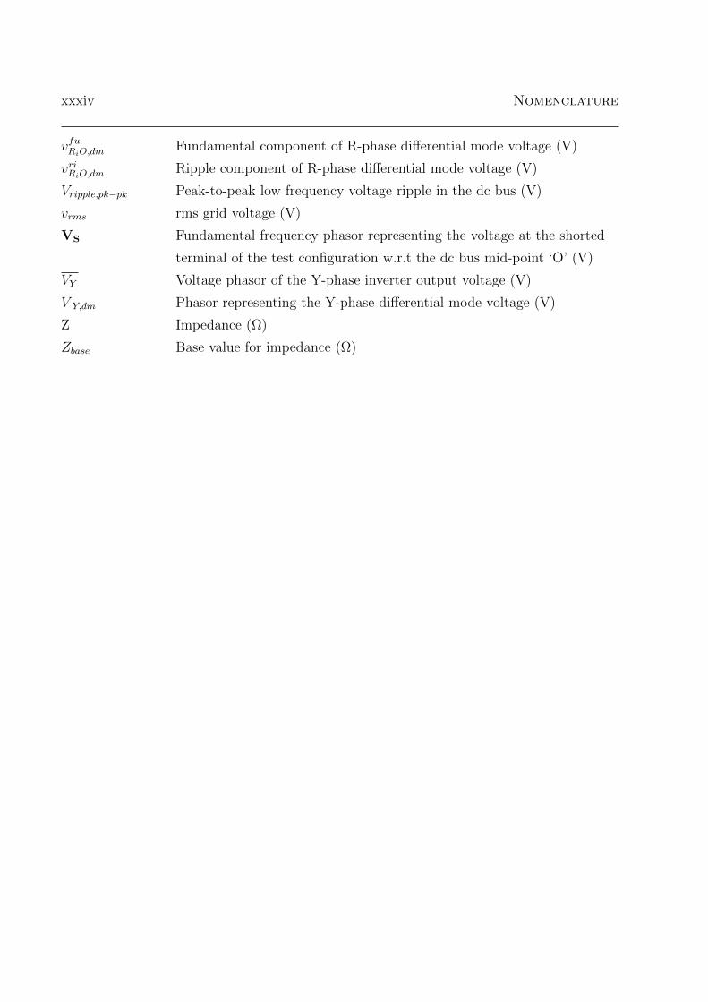
vfuRiO,dmFundamental component of R-phase differential mode voltage (V)
vriRiO,dmRipple component of R-phase differential mode voltage (V)
Vripple,pk−pk Peak-to-peak low frequency voltage ripple in the dc bus (V)
vrms rms grid voltage (V)
VS Fundamental frequency phasor representing the voltage at the shorted
terminal of the test configuration w.r.t the dc bus mid-point ‘O’ (V)
VY Voltage phasor of the Y-phase inverter output voltage (V)
V Y,dm Phasor representing the Y-phase differential mode voltage (V)
Z Impedance (Ω)
Zbase Base value for impedance (Ω)
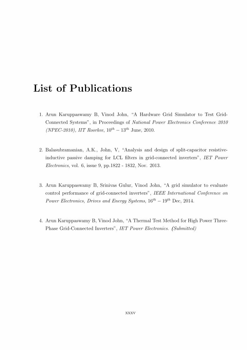
List of Publications
1. Arun Karuppaswamy B, Vinod John, “A Hardware Grid Simulator to Test Grid-
Connected Systems”, in Proceedings of National Power Electronics Conference 2010
(NPEC-2010), IIT Roorkee, 10th − 13th June, 2010.
2. Balasubramanian, A.K., John, V, “Analysis and design of split-capacitor resistive-
inductive passive damping for LCL filters in grid-connected inverters”, IET Power
Electronics, vol. 6, issue 9, pp.1822 - 1832, Nov. 2013.
3. Arun Karuppaswamy B, Srinivas Gulur, Vinod John, “A grid simulator to evaluate
control performance of grid-connected inverters”, IEEE International Conference on
Power Electronics, Drives and Energy Systems, 16th − 19th Dec, 2014.
4. Arun Karuppaswamy B, Vinod John, “A Thermal Test Method for High Power Three-
Phase Grid-Connected Inverters”, IET Power Electronics. (Submitted)
xxxv

xxxvi List of Publications

Chapter 1
Introduction
The last two decades has seen a phenomenal change in the way power is generated and
utilised. The use of grid-connected inverters is on the increase both at the point of generation
and utilisation. On the generation end, they are used to integrate renewable sources of power
with the ac grid. On the utility end, they find use in power factor correction, mitigation of
harmonics drawn from the grid and to improve the quality of voltage at the load terminals. In
all the above applications, it must be ensured that the switching frequency ripple injected into
the grid by the grid-connected inverter is within limits specified by the grid standards. This
requires a properly designed filter at the output of the inverter. Further, the grid-connected
inverter is expected to witness common grid disturbances like voltage sags, voltage swells
and the like. It should have controls that ensure its operation under these disturbances.
In this regard, the grid-connected inverters are expected to have good control performance.
Also, the required power handling capabilities of the grid-connected inverters has increased
and stands at a few MWs in the present day. This has necessitated research on general issues
related to grid-connected inverters and on specific issues related to their operation at high
power levels. As more of these converters are put to use, the research is towards making
these inverters more reliable.
In this thesis, the focus of studies has been on issues related to grid-connected inverters
and their operation at high power levels in the order of a few hundreds of kW and up into
the MW range in the contexts mentioned above.
Section 1.1 discusses the topology of grid-connected inverter considered in this thesis and
elaborates on its various applications. In Section 1.2, a survey of research in the area of
grid-connected inverters is provided. The relevant standards are also listed. The scope of
research in this thesis is discussed in Section 1.3. Section 1.4 provides the details of the
1

2
Gri
d
O
C
Dig
ital C
ontr
oller
G
rid
Voltages
Invert
er
Curr
ents
DC
Bus
Voltage
Load C
urr
ents
Inver
ter
Filte
rP
rote
ctio
n
Cir
cuits
Digital
Control
Fig
ure
1.1:
Gri
d-c
onnec
ted
inve
rter
.Sol
idlines
indic
ate
a3-
wir
eco
nfigu
rati
onan
ddas
hed
lines
indic
ate
a4-
wir
e
configu
rati
on.
Con
trol
inputs
dep
end
onth
eap
plica
tion
.
Chapter 1. Introduction 3
hardware set-up developed for the experimental evaluation. The organisation of the thesis
is outlined in Section 1.5. Section 1.6 summarises the Chapter.
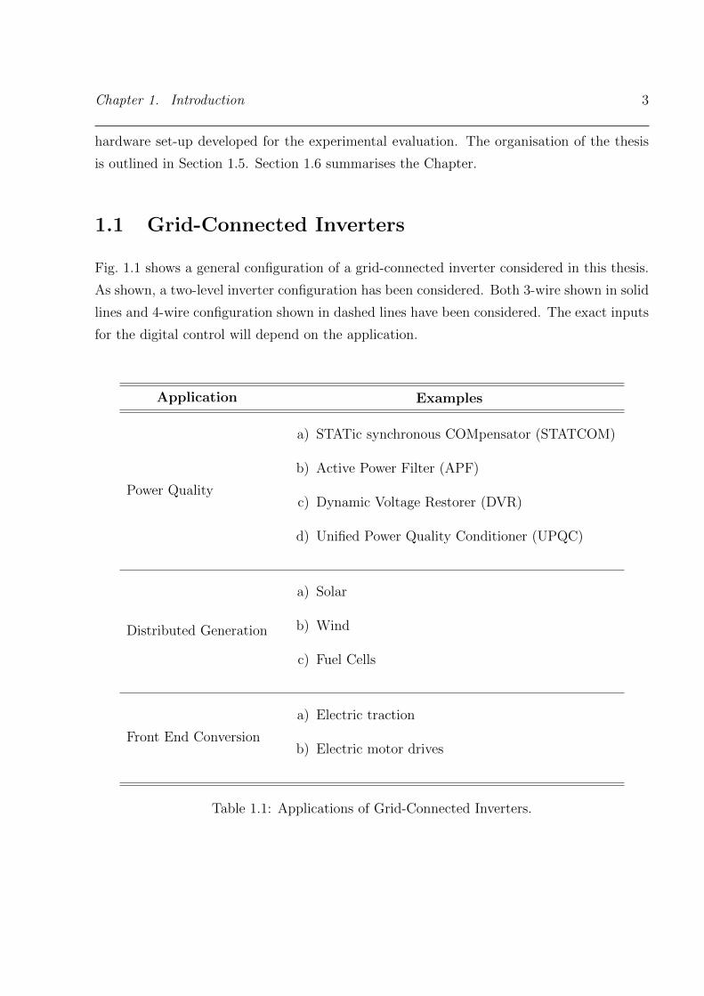
1.1 Grid-Connected Inverters
Fig. 1.1 shows a general configuration of a grid-connected inverter considered in this thesis.
As shown, a two-level inverter configuration has been considered. Both 3-wire shown in solid
lines and 4-wire configuration shown in dashed lines have been considered. The exact inputs
for the digital control will depend on the application.
Application Examples
Power Quality
a) STATic synchronous COMpensator (STATCOM)
b) Active Power Filter (APF)
c) Dynamic Voltage Restorer (DVR)
d) Unified Power Quality Conditioner (UPQC)
Distributed Generation
a) Solar
b) Wind
c) Fuel Cells
Front End Conversion
a) Electric traction
b) Electric motor drives
Table 1.1: Applications of Grid-Connected Inverters.

4 1.1. Grid-Connected Inverters
1.1.1 Applications
The simple configuration shown in Fig. 1.1 has a wide variety of applications which makes
it an important area of research in Power Electronics. The various applications have been
listed in Table 1.1:
1.1.1.1 Power Quality Applications
The grid-connected inverter can be used in shunt or series with the grid to solve several
power quality issues like power factor problems, voltage sags, voltage swells and harmonic
issues. The various power quality applications are described in detail below.
STATic synchronous COMpensator (STATCOM) Fig. 1.2 shows a grid-connected
inverter used as a STATCOM. In an application as a STATCOM [1, 2], the grid-connected
inverter is connected in shunt to the grid. The STATCOM dynamically supplies the reactive
power demanded by the load while only the real power is drawn from the grid. This reduces
the transmission losses incurred in transferring reactive currents from the generation point
to the load. Since the consumer is billed only for the real power drawn, the supplier usually
restricts the reactive currents that can be drawn by specifying power factor limits. The
superior dynamic performance of a STATCOM makes it more preferable than other power
factor correction alternatives such as fixed capacitor banks and Static Var Compensators
(SVCs).
Active Power Filter (APF) Fig. 1.3 shows an active power filter [3]. As can be ob-
served, the active power filter or a shunt active filter has a similar inverter configuration
as a STATCOM. The difference lies mainly in the control. The APF compensates for both
the fundamental frequency reactive current and the harmonic frequency currents demanded
by the load. While the STATCOM is useful for linear loads, the APF is more generic and
can maintain the current drawn from the grid to be near sinusoidal and at near unity power
factor for non-linear loads also.
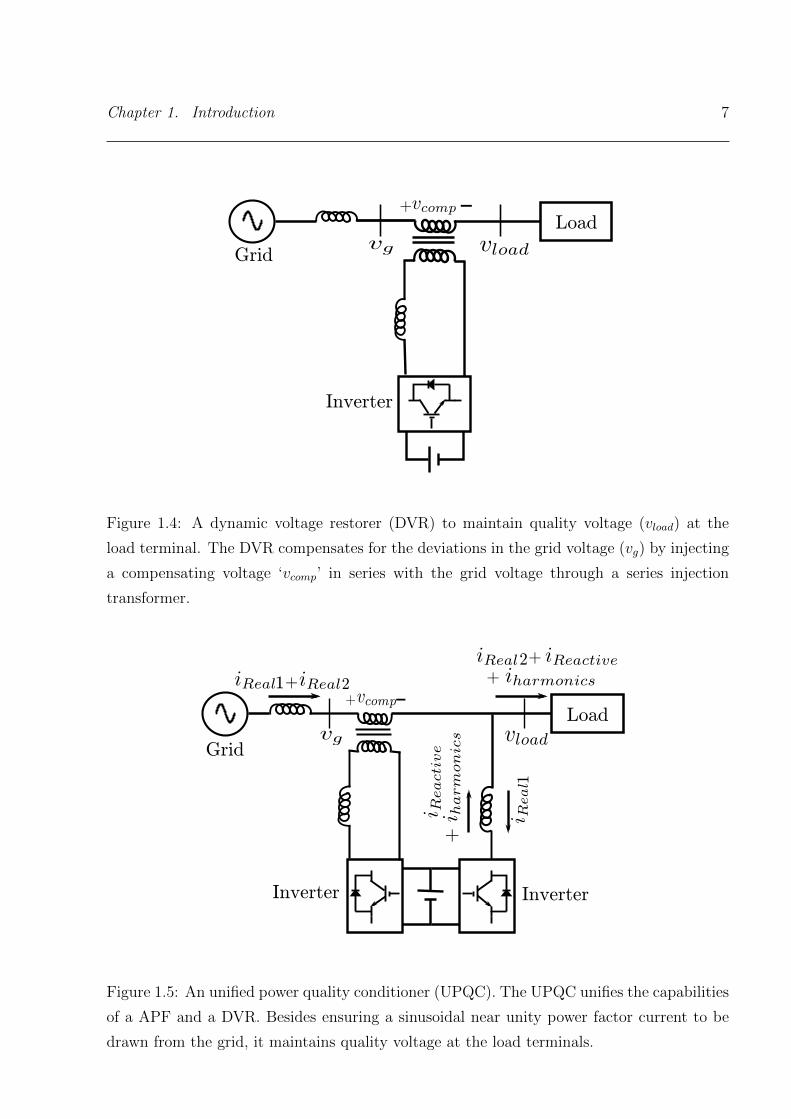
Dynamic Voltage Restorer (DVR) Fig. 1.4 shows a dynamic voltage restorer [4,5]. As
shown in the figure, the DVR is a series-connected inverter. The output voltage of the DVR,
‘vcomp’, is added in series with the grid voltage (vg) through a series-injection transformer.

Chapter 1. Introduction 5
Load
Grid
Inverter
Grid impedance
Outp
ut
filter
Figure 1.2: A STATCOM providing reactive power support to the load. The losses in
transmitting the reactive current from the grid to the load terminal is reduced. The power
factor is near unity for the fundamental frequency current drawn from the grid.
Load
Grid
Inverter
Grid impedance
Outp
ut
filter
Figure 1.3: An active power filter providing reactive and harmonic current support to the
load. The active power filter has the same topology as a STATCOM. The difference lies
mainly in the control. The active power filter compensates for the fundamental frequency
reactive current and the harmonic frequency current requirements of the load.
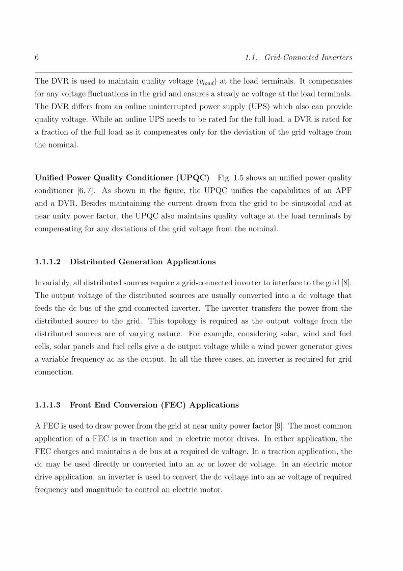
6 1.1. Grid-Connected Inverters
The DVR is used to maintain quality voltage (vload) at the load terminals. It compensates
for any voltage fluctuations in the grid and ensures a steady ac voltage at the load terminals.
The DVR differs from an online uninterrupted power supply (UPS) which also can provide
quality voltage. While an online UPS needs to be rated for the full load, a DVR is rated for
a fraction of the full load as it compensates only for the deviation of the grid voltage from
the nominal.
Unified Power Quality Conditioner (UPQC) Fig. 1.5 shows an unified power quality
conditioner [6, 7]. As shown in the figure, the UPQC unifies the capabilities of an APF
and a DVR. Besides maintaining the current drawn from the grid to be sinusoidal and at
near unity power factor, the UPQC also maintains quality voltage at the load terminals by
compensating for any deviations of the grid voltage from the nominal.
1.1.1.2 Distributed Generation Applications
Invariably, all distributed sources require a grid-connected inverter to interface to the grid [8].
The output voltage of the distributed sources are usually converted into a dc voltage that
feeds the dc bus of the grid-connected inverter. The inverter transfers the power from the
distributed source to the grid. This topology is required as the output voltage from the
distributed sources are of varying nature. For example, considering solar, wind and fuel
cells, solar panels and fuel cells give a dc output voltage while a wind power generator gives
a variable frequency ac as the output. In all the three cases, an inverter is required for grid
connection.
1.1.1.3 Front End Conversion (FEC) Applications
A FEC is used to draw power from the grid at near unity power factor [9]. The most common
application of a FEC is in traction and in electric motor drives. In either application, the
FEC charges and maintains a dc bus at a required dc voltage. In a traction application, the
dc may be used directly or converted into an ac or lower dc voltage. In an electric motor
drive application, an inverter is used to convert the dc voltage into an ac voltage of required
frequency and magnitude to control an electric motor.
Chapter 1. Introduction 7
Load
Grid
Inverter
+-
Figure 1.4: A dynamic voltage restorer (DVR) to maintain quality voltage (vload) at the
load terminal. The DVR compensates for the deviations in the grid voltage (vg) by injecting
a compensating voltage ‘vcomp’ in series with the grid voltage through a series injection
transformer.
Load
Grid
Inverter
+-
Inverter
1 2
1
2
Figure 1.5: An unified power quality conditioner (UPQC). The UPQC unifies the capabilities
of a APF and a DVR. Besides ensuring a sinusoidal near unity power factor current to be
drawn from the grid, it maintains quality voltage at the load terminals.
8 1.2. Research in the Area of Grid-Connected Inverters: An Overview
1.2 Research in the Area of Grid-Connected Inverters:
An Overview
The wide application of grid-connected inverters in recent years as elaborated in Section 1.1
has spurred research interest on inverters in general and grid-connected inverters in particu-
lar. The research primarily focuses on improving the reliability and performance of inverters.
Also, issues related to integration of inverters to the grid and their operation at high power
levels are of interest. Section 1.2.1 and Section 1.2.2 presents a survey of research in the field
of grid-connected inverters. The increased inter-connection of inverter with the grid and the
increasing power levels of these inverters have led to newer issues in the power grid. This
has initiated the development of new standards to ensure the stability and voltage quality in
the power grid. Section 1.2.3 discusses some standards relevant to grid-connected inverters.
The research work in this thesis focuses on certain aspects listed in this Section, the details
of which appears in Section 1.3.
1.2.1 Design Aspects
A survey of research on the design aspects of inverters when used as grid-connected converters
is presented below:
1.2.1.1 Topology
A wide variety of inverter topologies have been explored in literature [10–15]. Both single
phase [12,14] and three phase topologies [10,11,13] have been presented. Four leg topology
has been proposed [10] to eliminate the common mode voltage and for better utilisation of
the dc bus. Multi-level inverters have been developed for use at medium voltage levels [13].
The use of multi-level inverters has the advantage of requiring a lower blocking voltage across
the device during off-state and lower output voltage ripple [15]. Some of the topologies have
been suggested specifically for grid integration of renewable sources [11,12,14]. The two-level
inverter is the most commonly used topology of grid-connected inverters and is considered
in this thesis.

Chapter 1. Introduction 9
1.2.1.2 DC Bus Capacitor Selection
The ripple currents at the dc link, the connecting link between the dc bus capacitors and
the inverter IGBT modules, are supplied by the dc bus capacitors. The capacitance, ripple
current rating and lifetime of the dc bus capacitors are dependent on various parameters
such as the converter topology, modulation method, rating, operating dc bus voltage and
the load. A proper selection of dc bus capacitors is essential to ensure reliability of the
inverter. Reference [16] discusses the analytical computation of dc bus capacitor current to
aid the selection of dc bus capacitors for two level inverters. Reference [17] discusses the
same for a three level neutral point clamped inverter. Prediction of the lifetime of the dc
bus capacitors is of practical importance for inverter manufacturers and has been presented
in [18]. Analytical studies of current in dc bus capacitor can be used along with novel test
method proposed in this thesis to validate the design of the dc bus capacitors.
1.2.1.3 Busbar and Snubber Design
Busbars are used in power converters to minimize the inductance in the path connecting
the dc bus and the device terminals [19]. The inductance leads to voltage spikes across the
IGBTs during switching. The voltage spikes can damage the device. Further, the dv/dt
is a source of Electro Magnetic Interference (EMI) issues [20, 21]. The busbar design is
based on the nature and magnitude of the current flowing in the busbar, the temperature
rise of the bus plates and the power connections required at the modules and at the dc bus
capacitors. Further, the busbar design should ensure the inductance to be within allowable
limits. References [19,20,22] discuss some simple modelling techniques based on the busbar
geometry to compute the inductance while [21,23,24] discuss more accurate methods based
on electro-magnetics and finite element analysis. Some methods [21,22,24] in literature have
been developed for specific topologies like three-level topologies.
Snubbers are required in IGBT based inverters especially at high power levels to reduce
the stress on the device due to dv/dt, di/dt, over-voltage and short-circuit [25]. The main
purpose of snubber is to absorb the energy in the busbar inductance during switching.
The snubber provides an alternative path for the energy during switching thereby avoiding
voltage spikes across the device terminals. Snubbers may be associated with power losses as
most snubber topologies dissipate energy in resistors. Some designs attempt to lower this
loss [26]. Some other designs even attempt to develop inverter topologies that do not require

10 1.2. Research in the Area of Grid-Connected Inverters: An Overview
a snubber [27]. An effective busbar design and appropriate dc bus capacitor selection can be
used to eliminate the need for snubbers.
1.2.1.4 Output Filter Design
The IEEE has stringent recommendations [28] on the harmonics that can be injected into the
grid. This necessitates the use of a higher order LCL filter for grid-connected inverters. The
design of LCL filter depends on several factors such as the damping method used to suppress
the resonance introduced by the LCL filter, the switching frequency of the converter, the
modulation scheme and the operating dc bus voltage. Several LCL filter design methods
have been proposed in literature [29–33].
1.2.1.5 Output Filter Damping
The use of a third-order LCL filter introduces resonance which needs to be damped through
active or passive means. Passive damping is simple and robust but requires additional
components. Also, it leads to additional power loss in the filter. Active damping does not
require additional components and is lossless but adds control complexity. Both passive
damping [31,34] and active damping [35–37] are areas of active research.
1.2.1.6 Electro-Magnetic Interference (EMI) Filter Design
Electromagnetic interference issues arise due to high frequency switching. This can lead to
issues such as ground leakage currents, conducted EMI and radiated EMI. Both active [38,
39] and passive methods [40] of EMI filtering are proposed in literature. EMI models of
inverter [41] have also been developed to help device techniques that can mitigate EMI.
1.2.1.7 Thermal Design
The semiconductor devices in the inverter are sensitive to temperature. High temperatures
can lead to device failure. It must be ensured that the device junction temperatures are
maintained within datasheet specified limits. Research is aimed at developing thermal models
for inverters [42], developing closed form expressions and analytical methods to compute
conduction and switching losses [43] and study of materials used in the IGBT modules
that would lead to less junction temperature rise [44].The various models and analytical
expressions are generally used to optimize the inverter design from a thermal perspective [45].
Chapter 1. Introduction 11
1.2.2 Control Aspects
A survey of research on the control aspects of grid-connected inverters is presented below:
1.2.2.1 Modulation Techniques
Modulation techniques are used to convert the reference voltages of an inverter into the actual
output voltages. Modulation techniques are aimed at maximum utilization of the available
dc bus voltage and at reducing the instantaneous voltage error associated with the output
voltage. Sine triangle [46, 47], harmonic injection based pulse width modulation [46] and
various space vector based techniques [47,48] have been discussed in literature. Some Pulse
Width Modulation (PWM) methods are developed specifically for multi-level topologies [49,
50]. Carrier interleaved methods [51] help reduce common mode voltages and have also been
discussed in literature. Modulation techniques still remain an active area of research.
1.2.2.2 Phase Locked Loops
A Phase Locked Loop (PLL) is a vital control loop in grid-connected systems. The PLL
is required to synchronize the inverter to the grid and to keep it locked to the grid. Unit
vectors generated by the PLL are usually required for proper operation of the current control
loop. So, the PLL control is of importance. Research on PLLs [52–54] aim at improving the
operation of the PLL under real-time conditions like grid disturbances and sensor introduced
offsets.
1.2.2.3 Current Control
Current control in an inverter with output LCL filter is complex due to the presence of three
energy storage elements and the resonance associated with them. Several control methods
have been proposed in literature [33, 55–60]. Different controls such as a two current loop
control with an outer inductor current loop and an inner output capacitor current regulation
loop [55,59], model predictive method [58] and Proportional-Resonant (PR) controller based
control [60] have been investigated. Some controls aim at achieving balanced currents even
during unbalanced voltage dips [56].
12 1.3. Scope of the Thesis
1.2.2.4 Voltage Control
A fixed dc bus voltage is required in grid-connected inverters. Usually, a dc bus voltage
control loop is used to ensure this. For a two-level three-phase inverter topology with 3-wire
configuration, the dc bus voltage control is usually simple [2, 61]. However, in multi-level
inverter topologies the issue of balancing the individual dc bus capacitor voltages needs
attention. Several methods of dc bus voltage balancing have been suggested for multi-level
inverters [62–64]. While some methods achieve voltage balance through control [63,64], some
others suggest new topologies [62] to eliminate the problem.
1.2.3 Grid Connection Standards
IEEE and IEC have laid down several guidelines related to grid-connection. IEEE Standards
1547-2003 [28] and 519-1992 [65] specify limits on the harmonic currents that can be pumped
into the grid. Also, the increasing use of grid-connected inverters has initiated the develop-
ment of a new IEEE standard [66] for voltage sag and interruption ride-through testing of
electrical equipment.
The IEC has several standards for grid-connected systems. To mention a few, it has
recommendations for harmonic current limits [67], testing and measurement techniques for
voltage dips, short interruptions and voltage variation immunity [68, 69], testing and mea-
surement techniques for harmonics, interharmonics and low frequency immunity [70], specific
recommendations for wind turbines [71] and specific recommendations for photo voltaic in-
verters [72].
1.3 Scope of the Thesis
In this thesis, design and performance evaluation of sub-systems of grid-connected inverters
have been researched. The work touches upon areas discussed in Section 1.2.1.5 and Sec-
tion 1.2.1.7. Also, a test set-up to evaluate the compliance of grid-connected inverters to
some standards mentioned in Section 1.2.3 has been developed. An overview of the areas of
detailed investigation are:
1. LCL filter damping design
LCL filters are required in grid-connected inverters to comply with the IEEE recom-
mended harmonic limits [28, 65] on the current injected into the grid. LCL filters
Chapter 1. Introduction 13
introduce resonance. To damp it, either passive or active methods can be used. Pas-
sive methods are generally robust. Many passive damping networks are suggested in
literature [31,34]. However, a systematic component selection procedure has not been
developed for these networks. A simple and practical component selection procedure
would have wide industry application and is a focus of study in this thesis.
2. Thermal performance evaluation of high power grid-connected inverters
For reliability, grid-connected inverters need to be subjected to burn-in tests before
commissioning. To save energy during burn-in tests and to avoid the need for high
power sources and loads, regenerative methods have been developed [73–82]. However,
the available methods either require two converters of similar rating [73–80] or require
individual legs of the inverters to have independent cooling arrangement [81, 82]. A
method that addresses these issues would be of practical use. Also, methods for thermal
testing of the filter components and dc bus capacitors are not available currently. At
high power levels, these passive components also require attention. A test method for
thermal performance evaluation of grid-connected inverters and the associated passive
elements is a focus of study in this thesis.
3. Verification of control performance of grid-connected inverters
Present day grid-connected inverters are expected to have control capabilities to remain
in operation under short time grid disturbance conditions like voltage sags, voltage
swells and frequency deviations. To test these capabilities, a hardware that can gener-
ate the mentioned disturbance conditions in a controlled manner is required. Besides
generating sags, swells, unbalance and frequency deviations, the hardware should be
programmed to create point of fault conditions like phase jumps. A simple yet power-
ful algorithm is required for this. Available literatures focus on the topology [83–88]
used rather than the algorithm required for disturbance generation. Developing a test
set-up to generate grid disturbances in a controlled manner using a powerful algorithm
is a focus of study in this thesis.
1.4 Experimental Set-up
A 50kVA back-to-back connected inverter sharing a common dc bus has been custom-built for
the experimental studies. The output filters have been designed and fabricated to required
14 1.5. Organisation of the Thesis
specifications. The inverter set-up uses protection and gate drive circuits developed earlier,
in-house. The inverters are controlled using a common digital signal processor (DSP) board.
Texas Instrument’s TMS320F2812 has been used for digital control. Appendix A tabulates
the hardware details and provides some pictures of the experimental set-up.
1.5 Organisation of the Thesis
Chapter 1 discusses the relevance of research on grid-connected inverters. The topology used
and its wide application in power quality and distributed generation is detailed. A survey
of research in the area of grid-connected inverters is presented and the scope of the present
work is explained. The details of the experimental set-up developed for the work is provided
and the flow of the thesis is explained.
Chapter 2 discusses the design of output LCL filter and develops a component selection
procedure for a chosen passive damping topology. The Chapter begins with introducing the
relevant IEEE standard. The need for LCL filters in grid-connected inverters to comply
with the IEEE standards is brought out. The selection of ideal LCL filter components is
detailed. The issue of resonance is explained. Passive damping is suggested as a robust
means to damp the resonance. A comparison of the level of damping and damping resistor
power loss for three different passive damping topologies is provided. The SC-RL method
is chosen as a suitable topology for high power grid-connected inverters based on the power
loss. The state space model is developed for the SC-RL method using which its power loss
and damping are analysed. A component selection procedure is developed for the SC-RL
damping method with the goal of minimizing the losses in the damping resistor yet achieving
an effective damping. Experimental results are shown to have close match with the analytical
predictions.
Chapter 3 discusses the thermal performance evaluation of high-power grid-connected
inverters. The need for thermal testing of semiconductor devices and the passive components
associated with a grid-connected inverter is explained. The different methods available in
literature are discussed and the shortcomings of the available methods are pointed out. A new
method is proposed. Phasor diagrams are developed to give better insight into the operation
of the proposed method. Then, common mode and differential mode equivalent circuits
are developed and used for control design. Finally, the method is analysed in detail for the
thermal testing of semiconductor switches, dc bus capacitors and output filter components for
Chapter 1. Introduction 15
both three-phase 3-wire configuration and three-phase 4-wire configuration. Experimental
validation has also been provided.
In Chapter 4, a test set-up to study the control performance of grid-connected invert-
ers has been developed. The requirement of a test set-up to create grid disturbances in a
controlled manner in the laboratory environment is explained first. Then, the features of
simulators available in literature are explained and the focus in the present work is detailed.
The topology and controls used in the work are elaborated. A novel voltage disturbance
generation algorithm is developed and analysed using finite state machine model. Experi-
mental results of the grid simulator for linear, non-linear and inverter loads are provided to
practically validate the developed algorithm.
Chapter 5 summarises the contributions of the work done in this thesis. The implications
of the research work in terms of grid-connected inverter design is detailed.
1.6 Summary
In this Chapter, the wide application of grid-connected inverters is highlighted in the context
of power quality improvement and distributed generation applications. The topology of the
grid-connected inverter researched in this thesis has been briefed. A survey of research in the
area of grid-connected inverters is detailed and the specific areas of research touched upon
in this thesis is explained. An overview of the set-up built for the experimental validations
has been provided and the flow of the thesis has been detailed.

16 1.6. Summary
Chapter 2
LCL Filter Design
Electrical equipment have limits on the harmonic currents they can inject into the grid. IEEE
Standard 519–1992 [65] and IEEE Standard 1547–2003 [28] are some relevant standards that
specify the current harmonic limits. Usually, in case of distributed generation, power quality
applications and in front-end converter applications, an inverter connects to the grid. Hence,
this grid-connected inverter is expected to meet the mentioned standards in these cases. The
stringent requirements of these standards necessitate the use of a third order LCL filter at
the output of grid-connected inverters, which otherwise might use a simple L filter. In this
chapter, the design of LCL filter is discussed in detail with specific focus and contributions
on passive damping design for LCL filters.
Section 2.1 discusses the IEEE standards for connection of power sources to the grid.
The discussion brings out the need for LCL filters at the output of grid-connected inverters.
Section 2.2 explains the selection of LCL filter components based on the current harmonic
limits suggested by the IEEE standards. Section 2.3 details the issue of resonance associated
with LCL filters. The need for damping in LCL filters is shown. Section 2.4 analyses a
suitable passive damping method for LCL filter in high power grid-connected inverters. A
damping component selection procedure that maintains the damping circuit loss at a low
level and also provides adequate damping is proposed. Experimental results are provided to
support the analytical predictions. Section 2.5 summarises the Chapter.
17
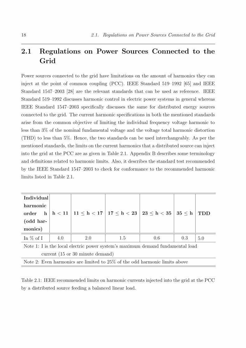
18 2.1. Regulations on Power Sources Connected to the Grid
2.1 Regulations on Power Sources Connected to the
Grid
Power sources connected to the grid have limitations on the amount of harmonics they can
inject at the point of common coupling (PCC). IEEE Standard 519–1992 [65] and IEEE
Standard 1547–2003 [28] are the relevant standards that can be used as reference. IEEE
Standard 519–1992 discusses harmonic control in electric power systems in general whereas
IEEE Standard 1547–2003 specifically discusses the same for distributed energy sources
connected to the grid. The current harmonic specifications in both the mentioned standards
arise from the common objective of limiting the individual frequency voltage harmonic to
less than 3% of the nominal fundamental voltage and the voltage total harmonic distortion
(THD) to less than 5%. Hence, the two standards can be used interchangeably. As per the
mentioned standards, the limits on the current harmonics that a distributed source can inject
into the grid at the PCC are as given in Table 2.1. Appendix B describes some terminology
and definitions related to harmonic limits. Also, it describes the standard test recommended
by the IEEE Standard 1547–2003 to check for conformance to the recommended harmonic
limits listed in Table 2.1.
Individual
harmonic
order h
(odd har-
monics)
h < 11 11 ≤ h < 17 17 ≤ h < 23 23 ≤ h < 35 35 ≤ h TDD
In % of I 4.0 2.0 1.5 0.6 0.3 5.0
Note 1: I is the local electric power system’s maximum demand fundamental load
current (15 or 30 minute demand)
Note 2: Even harmonics are limited to 25% of the odd harmonic limits above
Table 2.1: IEEE recommended limits on harmonic currents injected into the grid at the PCC
by a distributed source feeding a balanced linear load.

Chapter 2. LCL Filter Design 19
2.1.1 Need for LCL Filter in Grid-Connected Inverters
For pulse-width modulated (PWM) inverters with high carrier frequency, the ripple pre-
dominantly has frequency components at and around the switching frequency (ωsw) and its
multiples. Fig. 2.1 shows a typical voltage spectrum observed at the output terminals of
a 3-phase 2-level grid-connected inverter. Considering switching frequencies of 2 kHz and
above, the voltage harmonics appear at the harmonic order of h > 35. Hence, from Table 2.1,
it can be stated that all individual odd and even harmonic components should be limited
to 0.3% and 0.075% of the fundamental rated current respectively and the TDD should be
limited to 5%.
0 50 100 150 200 250 300 350 4000
0.1
0.2
0.3
0.4
0.5
0.6
0.7
0.8
0.9
1
1.1
1.2
Harmonic number (h)
rms
magn
itude
in p
.u w
ith fundam
enta
l rm
s vol
tage
as
the
bas
e
Output voltage = 240 V
Switching frequency = 10 kHz
DC bus voltage = 800 V
Sine triangle modulation, m = 0.85
Figure 2.1: Harmonic spectrum of terminal voltage measured with respect to dc bus mid-
point in a 3-phase 2-level inverter for a fundamental output voltage of 240 V and dc bus
voltage of 800 V. The spectrum is valid for the case when the inverter just balances the grid.
Switching frequency fsw considered is 10kHz.
20 2.2. LCL Filter Design
Let us attempt to use a simple first order L filter to achieve the required individual
harmonic limit for the spectrum shown in Fig. 2.1. Considering a 4-wire connection with
the neutral connected to the dc bus mid-point, the predominant harmonic component is
at h = 200. If the chosen filter limits the 200th harmonic component of current to within
0.075%, all the other individual harmonic components will surely be within the limits as the
impedance offered by the filter to all other harmonic components would almost be the same
or higher. For the 200th harmonic, V (p.u) = 0.9 and I (p.u) = 0.00075 (as per limits). So,
the required fundamental frequency impedance Z (p.u) is,
Z (p.u) = ω(p.u) · L(p.u) =V (p.u)
I(p.u) · 200= 6.0 p.u.
The p.u impedance of 6.0 is too high. Besides being bulky and costly, the high filter
impedance will increase the dc bus voltage requirement to impractical levels. The dc bus
voltage is chosen such that the maximum ac voltage that can be produced at the output of
the inverter will be able to balance the phasor sum of the grid voltage and the output filter
drop. An increase in the switching frequency can be thought of as a solution to maintain the
inductance value to be less and still maintaining the harmonic current limits. However, the
increased switching losses and the limitations on the maximum switching frequency of the
available devices will make it impossible. A higher order filter is the only viable solution.
A second order LC filter is not usually opted as both the inverter considered and the grid
are voltage sources and connecting a capacitor in parallel to a voltage source is redundant.
Hence, a third order LCL filter is generally used. The next Section explains the LCL filter
design.
2.2 LCL Filter Design
Fig. 2.2 shows the 3-phase 2-level inverter connected to the grid through a LCL filter. The
4-wire configuration gives the worst-case current ripple and is considered for the LCL filter
design. The design outcome can be used for a 3-wire configuration also though it would be
conservative. Reference [89] discusses a method of choosing the ideal LCL filter components
L1, L2 and C shown in Fig. 2.2. The design of the ideal LCL filter components used in
this work follows a similar methodology as [89]. However, there are significant differences
in the method developed in this thesis. This Section explains the selection of ideal LCL
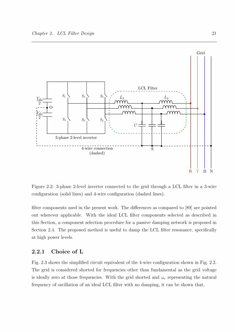
Chapter 2. LCL Filter Design 21
R Y B N
O
3-phase 2-level inverter
LCL Filter
Grid
S4-wire connection
(dashed)
Figure 2.2: 3-phase 2-level inverter connected to the grid through a LCL filter in a 3-wire
configuration (solid lines) and 4-wire configuration (dashed lines).
filter components used in the present work. The differences as compared to [89] are pointed
out wherever applicable. With the ideal LCL filter components selected as described in
this Section, a component selection procedure for a passive damping network is proposed in
Section 2.4. The proposed method is useful to damp the LCL filter resonance, specifically
at high power levels.
2.2.1 Choice of L
Fig. 2.3 shows the simplified circuit equivalent of the 4-wire configuration shown in Fig. 2.2.
The grid is considered shorted for frequencies other than fundamental as the grid voltage
is ideally zero at those frequencies. With the grid shorted and ωr representing the natural
frequency of oscillation of an ideal LCL filter with no damping, it can be shown that,
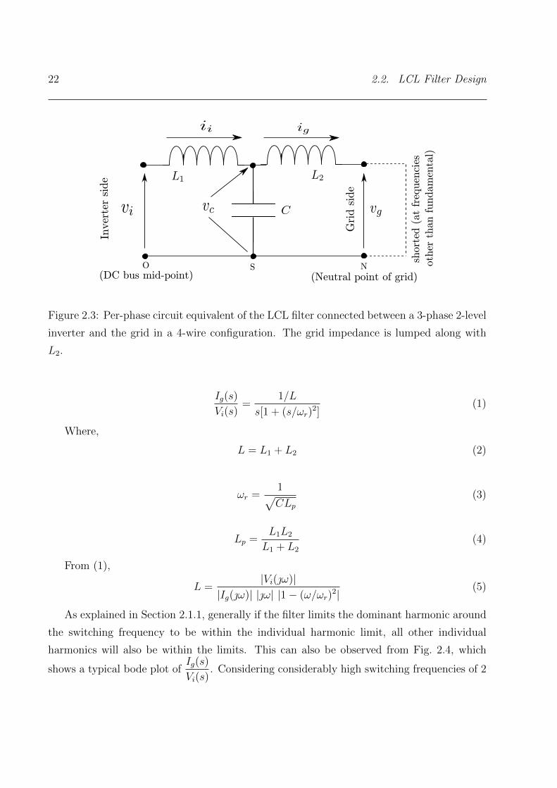
22 2.2. LCL Filter Design
Inver
ter
side
Gri
d s
ide
NO S(DC bus mid-point) (Neutral point of grid)
short
ed (
at
freq
uen
cies
oth
er t
han fundam
enta
l)
Figure 2.3: Per-phase circuit equivalent of the LCL filter connected between a 3-phase 2-level
inverter and the grid in a 4-wire configuration. The grid impedance is lumped along with
L2.
Ig(s)
Vi(s)=
1/L
s[1 + (s/ωr)2]
(1)
Where,
L = L1 + L2 (2)
ωr =1√CLp
(3)
Lp =L1L2
L1 + L2
(4)
From (1),
L =|Vi(ω)|
|Ig(ω)| |ω| |1− (ω/ωr)2|
(5)
As explained in Section 2.1.1, generally if the filter limits the dominant harmonic around
the switching frequency to be within the individual harmonic limit, all other individual
harmonics will also be within the limits. This can also be observed from Fig. 2.4, which
shows a typical bode plot ofIg(s)
Vi(s). Considering considerably high switching frequencies of 2
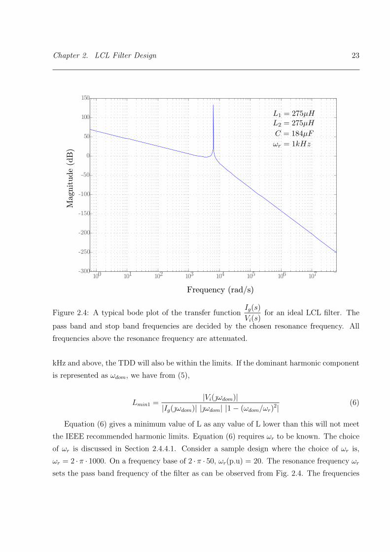
Chapter 2. LCL Filter Design 23
100 101 102 103 104 105 106 107-300
-250
-200
-150
-100
-50
0
50
100
150
Magnitude
(dB
)
Frequency (rad/s)
Figure 2.4: A typical bode plot of the transfer functionIg(s)
Vi(s)for an ideal LCL filter. The
pass band and stop band frequencies are decided by the chosen resonance frequency. All
frequencies above the resonance frequency are attenuated.
kHz and above, the TDD will also be within the limits. If the dominant harmonic component
is represented as ωdom, we have from (5),
Lmin1 =|Vi(ωdom)|
|Ig(ωdom)| |ωdom| |1− (ωdom/ωr)2|
(6)
Equation (6) gives a minimum value of L as any value of L lower than this will not meet
the IEEE recommended harmonic limits. Equation (6) requires ωr to be known. The choice
of ωr is discussed in Section 2.4.4.1. Consider a sample design where the choice of ωr is,
ωr = 2 · π · 1000. On a frequency base of 2 · π · 50, ωr(p.u) = 20. The resonance frequency ωr
sets the pass band frequency of the filter as can be observed from Fig. 2.4. The frequencies
24 2.2. LCL Filter Design
above the resonance frequency will be strongly attenuated. From, Fig. 2.1, the dominant
frequency is 200 p.u and its magnitude is 0.9 p.u. Reference [89] considers an approximate
value for the magnitude of the dominant frequency. In this thesis, an accurate actual p.u
magnitude from the spectral analysis is used. The dominant frequency being an even har-
monic greater than 35, the IEEE recommended harmonic current limit from Table 2.1 is
25% of 0.3%. Substituting the values of the various parameters in (6), we have,
Lmin1 =0.9
(0.25 ∗ 0.003) · (200) ·
∣∣∣∣∣1−(
200
20
)2∣∣∣∣∣
= 0.0606 (7)
The maximum value of L is limited to say 0.1 p.u, to avoid too high a value of dc bus
voltage requirement. Thus,
Lmax = 0.1 p.u (8)
Lmin1 and Lmax sets limits for L of the LCL filter. Observing (7), it can be seen that the
value of Lmin1 can be considerably reduced if even harmonics are not present in the voltage
spectrum as the current harmonic limits are too stringent for even harmonics. A proper
choice of switching frequency can remove the presence of even harmonics. For example,
the voltage harmonic spectrum for a switching frequency of 9.75 kHz is shown in Fig. 2.5.
Here, unlike in Fig. 2.1, the dominant harmonic is h = 195 which is odd. There are no even
harmonics present in the voltage spectrum. The value of Lmin1 in this case is 0.0167 p.u.
2.2.2 Choice of L1 and L2
Let,
L1 = aL · L2 (9)
Then, from (3) and (4),
L =(1 + aL)2
ω2r · aL · C
(10)
Reference [89] does not consider any limits on the reactive power requirement of the filter
capacitor. A lesser reactive power requirement of the filter capacitor at the fundamental
frequency or equivalently a lesser value of filter capacitance C is desirable. Hence a reactive
power limit for the capacitor is also used as a filter design constraint in this work. Also,
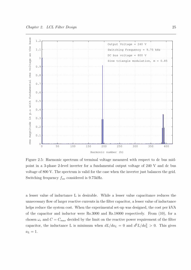
Chapter 2. LCL Filter Design 25
0 50 100 150 200 250 300 350 4000
0.1
0.2
0.3
0.4
0.5
0.6
0.7
0.8
0.9
1
1.1
1.2
Harmonic number (h)
rms magnitude in p.u with fundamental rms voltage as the base
Output Voltage = 240 V Switching Frequency = 9.75 kHz DC bus voltage = 800 V Sine triangle modulation, m = 0.85
Figure 2.5: Harmonic spectrum of terminal voltage measured with respect to dc bus mid-
point in a 3-phase 2-level inverter for a fundamental output voltage of 240 V and dc bus
voltage of 800 V. The spectrum is valid for the case when the inverter just balances the grid.
Switching frequency fsw considered is 9.75kHz.
a lesser value of inductance L is desirable. While a lesser value capacitance reduces the
unnecessary flow of larger reactive currents in the filter capacitor, a lesser value of inductance
helps reduce the system cost. When the experimental set-up was designed, the cost per kVA
of the capacitor and inductor were Rs.3000 and Rs.18000 respectively. From (10), for a
chosen ωr and C = Cmax decided by the limit on the reactive power requirement of the filter
capacitor, the inductance L is minimum when dL/daL = 0 and d2L/da2L > 0. This gives
aL = 1.

26 2.3. Resonance in LCL Filters
So,
L1 = L2 =L
2(11)
L2 includes the grid inductance. Using (10), based on the constraint on the reactive
current drawn by the capacitor, we have for aL = 1,
Lmin2 =4
ω2rCmax
(12)
L is chosen such that,
max(Lmin1, Lmin2) ≤ L ≤ Lmax (13)
As outlined in [89], L can be optimized for the power loss at this stage. Once it is
optimized at this stage, the selection of damping elements will not alter the power loss in
L significantly. This is because, the resonance frequency component of current is negligible
compared to the fundamental frequency and switching ripple components of current through
them and do not contribute much to their total power loss. Also, the damping elements do
not significantly alter the fundamental and switching ripple components of current through
L1 and L2.
2.2.3 Selection of C
Using (4) and (11), Lp = L/4. So, for the L chosen using (13), we have from (3),
C =4
ω2rL
(14)
2.3 Resonance in LCL Filters
Two resonances exist in an LCL filter that is connected at the output of a grid-connected
inverter. This section explains the origin of these resonances and the need for damping.
The resonances can be understood from the simplified per-phase equivalent circuit shown in
Fig. 2.3.
Chapter 2. LCL Filter Design 27
2.3.1 Parallel Resonance
This occurs when the parallel impedance of L2 and C becomes infinite at some frequency
ωp. ωp is the parallel resonance frequency. Ideally, this leads to zero current flow for any
voltage of that frequency present at the inverter output terminal since L2 ‖ C now appears
as a virtual open circuit.
We have,
ωpL2 ·1
ωpC
ωpL2 +1
ωpC
=∞ (15)
From (15), ωp =1√L2C
2.3.2 Series Resonance
This occurs when the parallel impedance of L2 and C gets cancelled by the impedance of L1
at some frequency ωs. ωs is the series resonance frequency. Under ideal circuit conditions,
this leads to infinite current flow for any voltage of that frequency present at the inverter
output terminal since the filter appears as a virtual short.
We have,
ωsL1 +
ωsL2 ·1
ωsC
ωsL2 +1
ωsC
= 0 (16)
From (16), ωs =1√LpC
It is desirable that the inverter output voltage should not contain components of voltage
at the resonance frequencies ωp and ωs. But, the switching transients and non-idealities
such as the dead-time can cause resonance frequency voltage components to appear at the

28 2.4. Damping Design for LCL Filter
inverter output terminals. So, the effect of resonances cannot be ignored. However, only
the series resonance is the one of concern as the current flow is zero in the case of parallel
resonance. It may be noted that this is because of the fact that a voltage source inverter
(VSI) is being considered currently.
The series resonance needs to be damped in order to avoid excessive current flow due to
excitation of the series resonance frequency. The damping can be done through active or
passive means. Passive damping does not require any complex control and is more reliable.
Hence, in the present work, a novel component selection procedure is developed for a passive
damping method and is used to contain the series resonance. The next Section discusses the
passive damping method in detail.
2.4 Damping Design for LCL Filter
Several passive damping methods have been suggested in literature. References [31] and [34]
give an almost exhaustive list of possible passive damping schemes. In this Section, some
selected schemes based on the simplicity of the circuitry are briefed. Then, a detailed anal-
ysis of the Split-Capacitor Resistive-Inductive (SC-RL) scheme is presented. The better
suitability of the SC-RL scheme as compared to the other schemes for use in high power
inverters is shown. The hardware being of higher power, the SC-RL scheme is chosen. A
novel component selection procedure is developed for the SC-RL passive damping scheme.
The proposed method performs the design selection of the damping network components one
at a time, optimizing the circuit parameters at each stage of addition of the components.
The method thus relies on a practical engineering method to passive network design rather
than on a purely multi-parametric mathematical optimization approach. The power loss in
the damping network and the level of damping are the cost functions used for optimization
at every stage.
2.4.1 Passive Damping Schemes
2.4.1.1 Purely Resistive (R) Damping Scheme
The purely resistive (R) damping scheme is the simplest of the damping schemes where a
damping resistor (Rd) is connected in series with the capacitor as shown in Fig. 2.6(a). The
drawback of this scheme is that all the components of current - fundamental, resonance and

Chapter 2. LCL Filter Design 29
L1 L2
vinverterRd
vgrid
C
(a)
Rd
Cd
C1
L1 L2
vinverter vgrid
(b)
L1
Cd
RdLd
L2
C1vgridvinverter
(c)
Figure 2.6: Passive damping schemes. (a) Purely Resistive (R) damping scheme. (b) Split-
Capacitor Resistive (SC-R) damping scheme. (c) Split-Capacitor Resistive-Inductive (SC-
RL) passive damping scheme.

30 2.4. Damping Design for LCL Filter
RdLd
C1
Ld Rd
C1
frequency)(at resonancefrequency)
(at switchingfrequency, itsmultiples andsidebands)
(at fundamental
CdCd Cd
Figure 2.7: Conceptual view of SC-RL damping scheme showing the predominant current
flow paths in the filter capacitor branch at different frequencies.
switching flow through the damping resistor Rd. So, the loss in Rd is high. However, this
method is suitable for low power inverters up to a few kVA due to the less component count.
2.4.1.2 Split-Capacitor Resistive (SC-R) Damping Scheme
Fig. 2.6(b) shows the Split-Capacitor Resistive (SC-R) damping scheme. Here, the switching
ripple gets predominantly by-passed through capacitor C1 and Rd finds only the fundamental
and resonance components flowing through it. So, the loss in Rd is moderate. This method
is suitable for inverter power levels in the range of a few kVA to few tens of kVA.
2.4.1.3 Split-Capacitor Resistive-Inductive (SC-RL) Damping Scheme
In the SC-RL damping scheme shown in Fig. 2.6(c), the fundamental frequency component of
current is largely by-passed through the damping inductor, Ld, the switching ripple currents
are largely by-passed through C1 and only the resonance current flows predominantly through
Rd. So, SC-RL damping scheme has very less loss in Rd and hence is suitable for high power
inverters ranging from a few tens of kVA up to around 1 MVA. Fig. 2.7 shows the conceptual
view of the SC-RL damping scheme.
It can be observed that the SC-RL damping scheme is an evolution over the R and SC-R
damping schemes in an attempt to reduce the loss in the damping resistor.
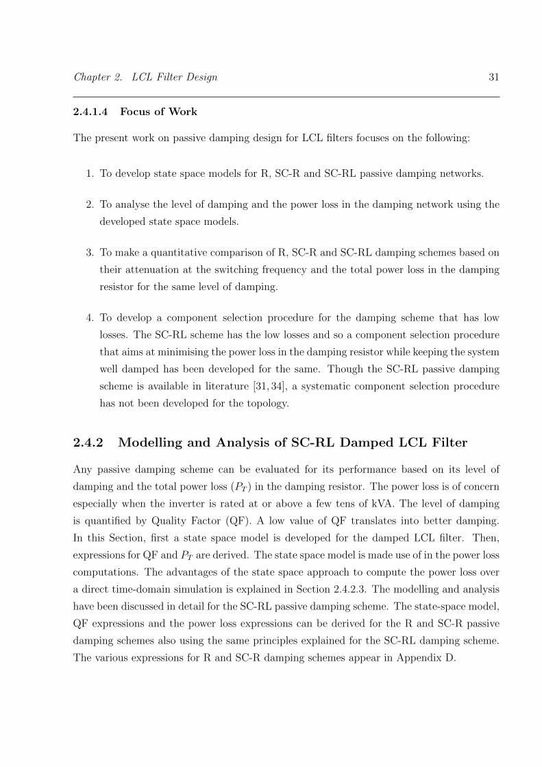
Chapter 2. LCL Filter Design 31
2.4.1.4 Focus of Work
The present work on passive damping design for LCL filters focuses on the following:
1. To develop state space models for R, SC-R and SC-RL passive damping networks.
2. To analyse the level of damping and the power loss in the damping network using the
developed state space models.
3. To make a quantitative comparison of R, SC-R and SC-RL damping schemes based on
their attenuation at the switching frequency and the total power loss in the damping
resistor for the same level of damping.
4. To develop a component selection procedure for the damping scheme that has low
losses. The SC-RL scheme has the low losses and so a component selection procedure
that aims at minimising the power loss in the damping resistor while keeping the system
well damped has been developed for the same. Though the SC-RL passive damping
scheme is available in literature [31, 34], a systematic component selection procedure
has not been developed for the topology.
2.4.2 Modelling and Analysis of SC-RL Damped LCL Filter
Any passive damping scheme can be evaluated for its performance based on its level of
damping and the total power loss (PT ) in the damping resistor. The power loss is of concern
especially when the inverter is rated at or above a few tens of kVA. The level of damping
is quantified by Quality Factor (QF). A low value of QF translates into better damping.
In this Section, first a state space model is developed for the damped LCL filter. Then,
expressions for QF and PT are derived. The state space model is made use of in the power loss
computations. The advantages of the state space approach to compute the power loss over
a direct time-domain simulation is explained in Section 2.4.2.3. The modelling and analysis
have been discussed in detail for the SC-RL passive damping scheme. The state-space model,
QF expressions and the power loss expressions can be derived for the R and SC-R passive
damping schemes also using the same principles explained for the SC-RL damping scheme.
The various expressions for R and SC-R damping schemes appear in Appendix D.
32 2.4. Damping Design for LCL Filter
+
_
+
+
_
_
+
_
at f
undam
enta
lfr
equen
cy
at a
ll f
requen
cies
oth
er t
han
fundam
enta
l
C1 vg
id
Rd
ig
vi
vd
ii
vC
Grid
O N(DC bus mid point) (Neutral)
L2L1
Cd
Ld iRdiLd
Inverter
Figure 2.8: An SC-RL damped LCL filter at the output of one phase of a three-phase 4-wire
inverter, showing the various state variables used to model the system.
2.4.2.1 Modelling of SC-RL Damped LCL Filter
The SC-RL damped LCL filter is modelled by considering one leg of a three-phase 4-wire
inverter as shown in Fig. 2.8. The state variables are chosen to be ii, ig, vC , vd and iLd.
From Fig. 2.8, the state equations and the output equation considering iRdas the output are
as follows:
diidt
=1
L1
vi −1
L1
vC (17)
digdt
=1
L2
vC −1
L2
vg (18)
dvCdt
=1
C1
[ii − ig − (iLd+vC − vdRd
)] (19)
dvddt
=1
Cd[iLd
+ (vC − vdRd
)] (20)
diLd
dt=
1
Ld(vC − vd) (21)
iRd=
1
Rd
[vC − vd] (22)
The state equations (17) to (21) and the output equation (22) can be represented in the

Chapter 2. LCL Filter Design 33
matrix form as,
x(t) = Ax(t) + Bu(t)
y(t) = Cx(t) + Du(t)(23)
Where,
A=
0 0 − 1
L1
0 0
0 01
L2
0 0
1
C1
− 1
C1
− 1
C1Rd
1
C1Rd
− 1
C1
0 01
CdRd
− 1
CdRd
1
Cd
0 01
Ld− 1
Ld0
; B=
1
L1
0
0 − 1
L2
0 0
0 0
0 0
; x=
ii
ig
vC
vd
iLd
;
u=
[vi
vg
]; C=
[0 0
1
Rd
− 1
Rd
0
]; D= [0 0]; y= iRd
;
The inputs to the model are the inverter output voltage, vi, and the grid voltage, vg. The
inverter voltage vi is either +Vdc/2 or −Vdc/2 depending on whether the top switch of the
inverter leg is ON or OFF respectively.
vi =
+Vdc2, 0 < t < ton
−Vdc2, ton < t < Tsw
(24)
where, ton is the time duration in a switching cycle when the top switch of the inverter leg
is ON and Tsw is the switching time period. The output of the model has been selected to
be iRdso that it can be used for loss evaluation in the damping circuit.
34 2.4. Damping Design for LCL Filter
Based on the above filter model, the quality factor and power loss of the SC-RL damped
LCL filter for a three-phase 4-wire configuration are derived in Section 2.4.2.2 and Sec-
tion 2.4.2.3 respectively. It may be noted that the model can be used even for a three-phase
3-wire case if vi is modified suitably to include the dc bus mid-point to output neutral voltage.
Equivalently, only the differential mode component of vi at every instant is to be considered
for a 3-wire case. The differential mode component of voltage is the actual voltage at the
inverter output terminal w.r.t the dc bus mid-point less the common mode component. The
common mode component of voltage at every instant can be computed as the average of the
three phase instantaneous voltages at the output terminals of the inverter.
2.4.2.2 Quality Factor (QF)
In Fig. 2.8, VC(s)/Vi(s) – the capacitor voltage to inverter leg voltage, is the representative
transfer function that is used to study the damping of the series resonance in the present work.
Fig. 2.9 shows a typical plot of the transfer function VC(s)/Vi(s). The difference in magnitude
between the resonance peak of the curve and the flat portion of the curve defines the quality
factor (QF). The flat portion of the curve extends from dc to near resonance frequency. The
nature of the bode plot explains the choice of the transfer function VC(s)/Vi(s). The QF
can be easily defined using this transfer function rather than for example, using the transfer
function Ig(s)/Vi(s) shown for an ideal LCL filter in Fig. 2.4.
Mathematically, the QF can be expressed as,
QF =
∣∣∣∣VC(jω)
Vi(jω)
∣∣∣∣at ω = ωd∣∣∣∣VC(jω)
Vi(jω)
∣∣∣∣ω → 0
(25)
where, ωd is the resonance frequency of the LCL filter with the damping components
included. ωd is that value of ω for which the magnitude of the transfer function (26) peaks.
A detailed discussion of QF in the context of LCL filter design appears in Appendix C.
From Fig. 2.8, considering the grid side voltage source as a short, VC(s)/Vi(s) can be
shown to be,
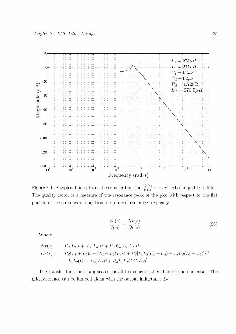
Chapter 2. LCL Filter Design 35
100
101
102
103
104
105
106
107
-140
-120
-100
-80
-60
-40
-20
0
20
Magnitude
(dB
)
Frequency (rad/s)
Figure 2.9: A typical bode plot of the transfer function VC(s)Vi(s)
for a SC-RL damped LCL filter.
The quality factor is a measure of the resonance peak of the plot with respect to the flat
portion of the curve extending from dc to near resonance frequency.
VC(s)
Vi(s)=Nr(s)
Dr(s)(26)
Where,
Nr(s) = Rd L2 s+ L2 Ld s2 +Rd Cd L2 Ld s
3;
Dr(s) = Rd(L1 + L2)s+ (L1 + L2)Lds2 +Rd[L1L2(C1 + Cd) + LdCd(L1 + L2)]s
3
+L1L2(C1 + Cd)Lds4 +RdL1L2C1CdLds
5.
The transfer function is applicable for all frequencies other than the fundamental. The
grid reactance can be lumped along with the output inductance L2.
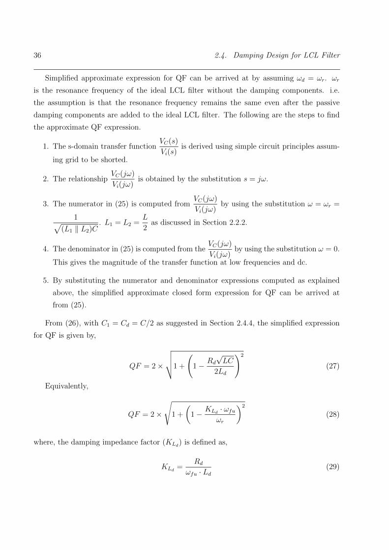
36 2.4. Damping Design for LCL Filter
Simplified approximate expression for QF can be arrived at by assuming ωd = ωr. ωr
is the resonance frequency of the ideal LCL filter without the damping components. i.e.
the assumption is that the resonance frequency remains the same even after the passive
damping components are added to the ideal LCL filter. The following are the steps to find
the approximate QF expression.
1. The s-domain transfer functionVC(s)
Vi(s)is derived using simple circuit principles assum-
ing grid to be shorted.
2. The relationshipVC(jω)
Vi(jω)is obtained by the substitution s = jω.
3. The numerator in (25) is computed fromVC(jω)
Vi(jω)by using the substitution ω = ωr =
1√(L1 ‖ L2)C
. L1 = L2 =L
2as discussed in Section 2.2.2.
4. The denominator in (25) is computed from theVC(jω)
Vi(jω)by using the substitution ω = 0.
This gives the magnitude of the transfer function at low frequencies and dc.
5. By substituting the numerator and denominator expressions computed as explained
above, the simplified approximate closed form expression for QF can be arrived at
from (25).
From (26), with C1 = Cd = C/2 as suggested in Section 2.4.4, the simplified expression
for QF is given by,
QF = 2×
√√√√1 +
(1− Rd
√LC
2Ld
)2
(27)
Equivalently,
QF = 2×
√1 +
(1− KLd
· ωfuωr
)2
(28)
where, the damping impedance factor (KLd) is defined as,
KLd=
Rd
ωfu · Ld(29)
Chapter 2. LCL Filter Design 37
KLdis a function of Ld and it can be interpreted as that multiple of fundamental frequency
(ωfu) at which the damping resistance equals the impedance of the damping inductor. It
can be observed later that KLdis unitless and serves as a generalized design parameter.
It can be seen from (28) that the minimum QF occurs for KLd= ωr/ωfu = ωr(p.u.).
However, the addition of the damping circuit will actually alter the resonance frequency of
the LCL filter. The refined value of KLddue to the modified resonance frequency is obtained
numerically as described in Section 2.4.4.3. The usefulness of (28) is that it indicates a
possible relationship between KLdand ωr(p.u.). A detailed discussion on this appears in
Section 2.4.4.4.
2.4.2.3 Power Loss
The power loss primarily consists of two components - the fundamental frequency component,
Pfu, and the switching ripple component, Pri. The switching frequency is well separated
from the resonance frequency and does not excite any resonance component in steady state.
However, in the hardware small resonance components that are excited by the transients
and other sources such as switch non-idealities are usually observed. The QF being low, the
current and hence the power loss due to this is negligible and is not considered for the total
power loss (PT ) computations.
Loss due to fundamental frequency current: From Fig. 2.8, the fundamental power
loss component, Pfu, in the damping resistor of the filter can be obtained as follows:
Pfu = <VC I∗d|ω=ωfu(30)
From the circuit analysis of Fig. 2.8, we can express Pfu as,
Pfu = <
VC V
∗C[
jωfu Ld Rd
Rd + jωfu Ld+
1
jωfu Cd
]∗ (31)
At fundamental frequency, the voltage magnitude at the inverter and the grid are close to 1
p.u. So, VC can be approximated to be 1 p.u as the voltage drop in the filter inductors L1

38 2.4. Damping Design for LCL Filter
and L2 is less. Substituting all quantities in per unit, we have,
Pfu(p.u.) =C2dRd
K2Ld− 2CdRdKLd
+ (1 + C2dR
2d)
(32)
The denominator function in (32) represents a parabola with a symmetry parallel to the
y-axis when KLdis plotted in the x-axis and the value of the function is plotted along the
y-axis. Since the magnitude of a parabola increases rapidly with x-axis value, Pfu which is
an inverse function falls to a low value quickly and changes very less there after. This can be
observed in the fundamental frequency power loss curve of Fig. 2.14 shown in Section 2.4.4.
The fundamental frequency power loss curve has a knee point as expected. After the knee
point, the power loss almost remains a constant. So, any value of KLdafter the knee point
is a good choice from the perspective of Pfu.
Loss due to switching ripple current: Using the state space model given by (23),
the loss due to the switching ripple component of current that comprises of the switching
frequency, its multiples and sidebands can be computed. The computation of iRdand iRd,rms
is given in detail in Section 2.4.2.4. The ripple current is dependent on the duty ratio d,
which varies every switching cycle. The worst-case condition of switching that leads to high
rms ripple current is that of a square wave, which occurs for the case of zero fundamental
voltage. This corresponds to a duty ratio, d = 0.5 and has been used in the computation of
Pri from a worst case power loss consideration.
By substituting quantities in p.u, the power loss due to the ripple component of current
can be computed as,
Pri(p.u.) = (iRd,rms)2 ·Rd (33)
Total power loss in the damping resistor: Using (32) and (33), the total power loss
in the damping resistor can be computed as,
PT (p.u.) = Pfu(p.u.) + Pri(p.u.) (34)
2.4.2.4 Computation of iRd,rms
From (23), it can be observed that iRdis a linear combination of the state variables. So,
the computation of iRdand hence iRd,rms for a given duty ratio d requires solving the state
equation (23). Since the ripple current is the parameter of interest, the computation need

Chapter 2. LCL Filter Design 39
to be done over a switching time interval, Tsw only. Following is the step-by-step procedure
to compute iRdfor a given duty ratio d:
1. The solution for (23) is given by [90],
x(t) = eAtx(0) +
∫ t
0
eA(t−τ)Bu(τ)dτ (35)
From (23), ‘A’ is a 5x5 matrix for the LCL filter with SC-RL damping. So, to simplify
the computations and to avoid matrix inversion error in the computation of the initial
condition for the solution in later steps, the actual model in terms of x(t) is transformed
into its diagonal form in terms of x(t) using similarity transformation. The similarity
transformation helps break down the vector x(t) of larger dimension into multiple
vectors x(t) of smaller dimensions which can be solved easily. Numerical values of the
filter parameters are used for the transformation.
Let us consider a numerical example with L1 = 275µH, L2 = 275µH, C1 = 92µF ,
Cd = 92µF , Rd = 1.728Ω and Ld = 500µH. For the chosen set of filter values, we have
from (23),
A=
0 0 −3636.4 0 0
0 0 3636.4 0 0
10869.6 −10869.6 −6290.3 6290.3 −10869.6
0 0 6290.3 −6290.3 10869.6
0 0 2000 −2000 0
;
B=
3636.4 0
0 −3636.4
0 0
0 0
0 0
; x=
ii
ig
vC
vd
iLd
; u=
[vi
vg
];

40 2.4. Damping Design for LCL Filter
C= [0 0 0.579 − 0.579 0]; D= [0 0]; y= iRd;
Similarity Transformation:
The eigen values of the above system are λ1,2 = −4094.6 ± 6242.5, λ3 = 0, λ4,5 =
−2195.8± 5100.4 and the eigen vector matrix is,
Q=
−0.25 + 0.07 −0.25− 0.07 −0.707 −0.18 + 0.19 −0.18− 0.19
0.25− 0.07 0.25 + 0.07 −0.707 0.18− 0.19 0.18 + 0.19
−0.17 + 0.50 −0.17− 0.50 0 0.15 + 0.37 0.15− 0.37
0.72 0.72 0 0.80 0.80
0.24 + 0.13 0.24− 0.13 0 0.21 + 0.16 0.21− 0.16
;
Comparing Q with, Q= [q1 q2 q3 q4 q5], let, P−1 = [<(q1) =(q1) q3 <(q4) =(q4)].
Then,
P=
−1.72 1.72 −1.26 −2.37 6.80
−3.33 3.33 2.24 −2.62 2.53
−0.71 −0.71 0 0 0
1.55 −1.55 1.14 3.39 −6.14
3.097 −3.10 −1.36 1.09 2.16
;
The similarity transformation equations, A = PAP−1, B = PB, C = CP−1, D = D
and X = PX give,

Chapter 2. LCL Filter Design 41
A=
−4094.6 6242.5 0 0 0
−6242.5 −4094.6 0 0 0
0 0 0 0 0
0 0 0 −2195.8 5100.4
0 0 0 −5100.4 −2195.8
=
A1 0 0
0 A2 0
0 0 A3
;
B=
−6257.19 −6257.19
−12090.12 −12090.12
- - - - - - - - - - - - - - - - - - -
−2571.32 2571.32
- - - - - - - - - - - - - - - - - - -
5651.56 5651.56
11261.17 11261.17
=
B1
B2
B3
;
C= [−0.51 0.29 : 0 : − 0.38 0.21] =[C1C2C3
]; D= [0 0];
x=
−1.72 1.72 −1.26 −2.37 6.80
−3.33 3.33 2.24 −2.62 2.53
−0.71 −0.71 0 0 0
1.55 −1.55 1.14 3.39 −6.14
3.097 −3.10 −1.36 1.09 2.16
ii
ig
vC
vd
iLd
=
x1
x2
x3
; u=
[vi
vg
];
Matrix A shows that the fifth order system has been transformed into three systems
– two of second order and one of first order. The state space representation of the
reduced order systems is given by,

42 2.4. Damping Design for LCL Filter
˙xl(t) = Alxl(t) + Blu(t)(36)
where, l = 1,2,3 and the output equation is given by,
y(t) = Cx(t) + Du(t)(37)
2. The number of independent reduced order systems resulting from the similarity trans-
formation depend on the nature of the poles. Each real pole and each set of complex
conjugate poles lead to an independent system. For a SC-RL damped LCL filter, there
can be one real pole and two sets of complex conjugate poles or three real poles and
a set of complex conjugate poles depending on the choice of parameters. This can be
observed from the pole-zero plot, Fig. 2.18. So, there are either 3 or 4 sets of indepen-
dent equations for the SCRL damped LCL filter. The solution for each of the simpler
vectors xl(t) is given by,
xl(t) = eAltxl(0) +
∫ t
0
eAl(t−τ)Blu(τ)dτ (38)
where, l = 1,2,3 or l = 1,2,3,4 depending on the nature of the poles.
3. Considering the switching time period, Tsw, to be divided into n small sampling time
intervals of duration Tsmpl, the discrete-time equivalent of (38) is [90],
xl[m + 1] = eAlTsmplxl[m]−(∫ Tsmpl
0
eAlαdα
)Blu[m] (39)
with, n = sample points in one switching cycle =TswTsmpl
.
n has been taken to be 200 for the numerical computations in the present work.
4. Using (39), xl[m] is computed at intervals of Tsmpl for the required duty ratio, d. The
computation of xl[m] requires the initial condition xl[0] and the inputs vi and vg. xl[0]
is taken to be the equilibrium point at the desired duty ratio d. The computation
and use of equilibrium point as the initial condition for solving the state equations is
Chapter 2. LCL Filter Design 43
explained after Step 5. Input vi is given by (24) with ton = dTsw. Input vg is the
grid voltage corresponding to the chosen duty ratio and is given by, Vdc · (d − 0.5).
This choice of vg assumes that there is no current flowing between the inverter and the
grid. i.e. the inverter just balances the grid. Since the switching ripple current is the
parameter of interest and as the voltage drop in the filter is negligible, this assumption
is considered valid.
5. From xl[m], x[m] is found using inverse transformation. Then, using (23), iRd[m] can
be computed as,
iRd[m] =
(x3[m]− x4[m])
Rd
=vC [m]− vd[m]
Rd
(40)
Equilibrium Points: For a given time period of computation, the equilibrium point gives
the initial value for which the state would return to the same value at the end of the compu-
tation. The switching ripple component of currents and voltages are the parameters being
computed. In steady state, assuming the fundamental component of currents and voltages
to be constant over a switching time period, the switching ripple component will be at equi-
librium. i.e. the switching ripple components of currents and voltages return to their initial
value at the end of the switching time period. This is equivalent to invoking the inductor
volt-sec balance and the capacitor charge-balance [91] over a switching cycle. The equilib-
rium points can be used as initial condition to compute successive discrete time values using
(39) for a given duty ratio d. It may be noted that an approximation is made in the above
discussion as the fundamental component of currents and voltages do change slightly though
insignificantly over a switching time period. So, actually a quasi-steady state approximation
is used.
Using (38) and considering Tsw to be the switching time period, we have
xl(Tsw) = eAlTsw xl(0) +
∫ dTsw
0
eAl(Tsw−τ)Blu(τ)dτ
+
∫ Tsw
dTsw
eAl(Tsw−τ)Blu(τ)dτ (41)
In steady state – for a given duty ratio d – by invoking equilibrium, we have, xl(Tsw) = xl(0).

44 2.4. Damping Design for LCL Filter
Using this in (41) and solving for xl(0), the equilibrium points can be obtained as,
xl(0) = [I− eAlTsw ]−1
∫ dTsw
0
eAl(Tsw−τ)Blu(τ)dτ
+
∫ Tsw
dTsw
eAl(Tsw−τ)Blu(τ)dτ
(42)
From (42), it can be observed that there is a possibility of matrix inversion error due
to poles present at origin. The damped LCL filter has one pole at the origin. So, in the
transformed state equations, one of the equations would lead to matrix inversion error. For
the LCL filter with the proposed damping method, the inversion problem occurs always for
the state variable which is a scaled sum of the currents through L1 and L2. This can be
observed from the matrix A and the vector x.
Let us assume an intial condition that,
iL1 + iL2 = 0 (43)
Then, the state variable with the inversion problem has an initial condition of zero and,
iL1 = −iL2 (44)
From Step 4 in the computation of iRd,rms, vi = vg. So, by symmetry, since L1 = L2, iL1
should be equal to −iL2 . So, our assumption of initial condition is valid. So, we can solve
the system. It may be noted that we are avoiding the matrix inversion error through our
knowledge of the physical circuit.
Computation of iRd,rms: The rms value of iRdfor a given duty ratio d is,
iRd,rms =
√√√√ 1
n
n∑m=0
(iRd[m])2 (45)
Knowing iRd,rms for d = 0 to 1 for a quasi-steady state condition, the rms switching
ripple current in the damping resistor over one fundamental cycle of time period T, for a
sinusoidally varying inverter output voltage is given by,
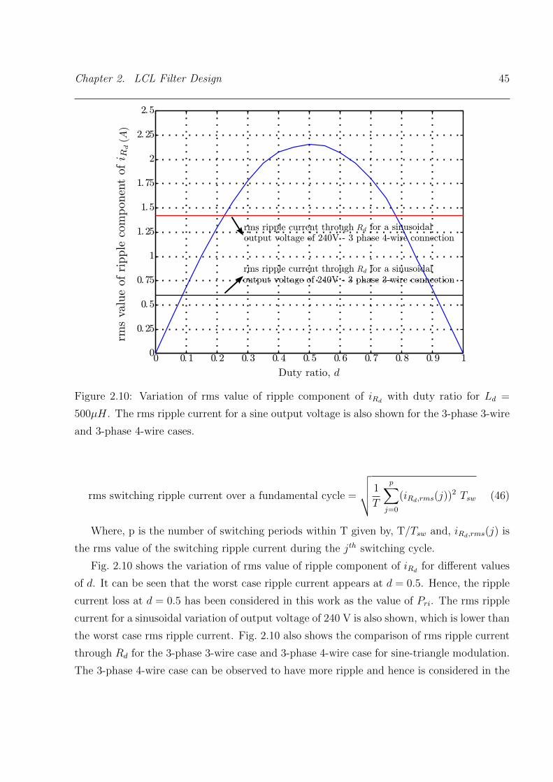
Chapter 2. LCL Filter Design 45
0 0.1 0.2 0.3 0.4 0.5 0.6 0.7 0.8 0.9 10
0.25
0.5
0.75
1
1.25
1.5
1.75
2
2.25
2.5
rms ripple current through for a sinusoidal
output voltage of 240V - 3 phase 4-wire connection
rms ripple current through for a sinusoidal
output voltage of 240V - 3 phase 3-wire connection
Figure 2.10: Variation of rms value of ripple component of iRdwith duty ratio for Ld =
500µH. The rms ripple current for a sine output voltage is also shown for the 3-phase 3-wire
and 3-phase 4-wire cases.
rms switching ripple current over a fundamental cycle =
√√√√ 1
T
p∑j=0
(iRd,rms(j))2 Tsw (46)
Where, p is the number of switching periods within T given by, T/Tsw and, iRd,rms(j) is
the rms value of the switching ripple current during the jth switching cycle.
Fig. 2.10 shows the variation of rms value of ripple component of iRdfor different values
of d. It can be seen that the worst case ripple current appears at d = 0.5. Hence, the ripple
current loss at d = 0.5 has been considered in this work as the value of Pri. The rms ripple
current for a sinusoidal variation of output voltage of 240 V is also shown, which is lower than
the worst case rms ripple current. Fig. 2.10 also shows the comparison of rms ripple current
through Rd for the 3-phase 3-wire case and 3-phase 4-wire case for sine-triangle modulation.
The 3-phase 4-wire case can be observed to have more ripple and hence is considered in the
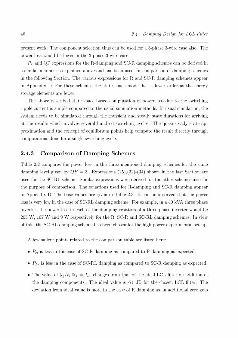
46 2.4. Damping Design for LCL Filter
present work. The component selection thus can be used for a 3-phase 3-wire case also. The
power loss would be lower in the 3-phase 3-wire case.
PT and QF expressions for the R-damping and SC-R damping schemes can be derived in
a similar manner as explained above and has been used for comparison of damping schemes
in the following Section. The various expressions for R and SC-R damping schemes appear
in Appendix D. For these schemes the state space model has a lower order as the energy
storage elements are fewer.
The above described state space based computation of power loss due to the switching
ripple current is simple compared to the usual simulation methods. In usual simulation, the
system needs to be simulated through the transient and steady state durations for arriving
at the results which involves several hundred switching cycles. The quasi-steady state ap-
proximation and the concept of equilibrium points help compute the result directly through
computations done for a single switching cycle.
2.4.3 Comparison of Damping Schemes
Table 2.2 compares the power loss in the three mentioned damping schemes for the same
damping level given by QF = 3. Expressions (25),(32)-(34) shown in the last Section are
used for the SC-RL scheme. Similar expressions were derived for the other schemes also for
the purpose of comparison. The equations used for R-damping and SC-R damping appear
in Appendix D. The base values are given in Table 2.3. It can be observed that the power
loss is very low in the case of SC-RL damping scheme. For example, in a 40 kVA three phase
inverter, the power loss in each of the damping resistors of a three-phase inverter would be
205 W, 107 W and 9 W respectively for the R, SC-R and SC-RL damping schemes. In view
of this, the SC-RL damping scheme has been chosen for the high power experimental set-up.
A few salient points related to the comparison table are listed here:
• Pri is less in the case of SC-R damping as compared to R-damping as expected.
• Pfu is less in the case of SC-RL damping as compared to SC-R damping as expected.
• The value of |ig/vi|@f = fsw changes from that of the ideal LCL filter on addition of
the damping components. The ideal value is -71 dB for the chosen LCL filter. The
deviation from ideal value is more in the case of R damping as an additional zero gets
Chapter 2. LCL Filter Design 47
Parameter R Damping SC-R Damping SC-RL Damping
fsw 9.75kHz 9.75kHz 9.75kHz
fr 1kHz 1kHz 1kHz
L1(p.u.) 0.02 0.02 0.02
L2(p.u.) 0.02 0.02 0.02
C(p.u.) 0.25 - -
C1(p.u.) - 0.125 0.125
Cd(p.u.) - 0.125 0.125
Rd(p.u.) 0.0718 0.484 0.4
Ld(p.u.) - - 0.0201
|ig/vi|@f = fsw -59 dB -65 dB -65 dB
QF 3.0 3.0 3.0
Pfu(%) 0.45 0.75 0.0016
Pri(%) 1.09 0.05 0.065
PT (%) 1.54 0.80 0.0666
Table 2.2: Comparison of R, SC-R and SC-RL damping schemes.
48 2.4. Damping Design for LCL Filter
added into the system in R damping which changes the nature of the high frequency
attenuation characteristics.
• The minimum required attenuation is -63.33 dB for the chosen LCL filter to follow the
IEEE standards. It can be seen that SC-R and SC-RL damping satisfies this.
2.4.4 SC-RL Damping Circuit Design
The system under consideration being of higher order, adding one component at a time to the
design would lead to a simplified procedure of component selection. Also, a multi-parameter
numerical optimization approach to the damping circuit may not provide adequate design
insight. So, the approach of adding damping components in steps to the ideal LCL filter
has been used. At each step, the selection of the component being added is based on the
objective of maintaining both QF and PT to be low. First, L1, L2 and C are chosen for
an ideal LCL filter as explained in Section 2.2. Then, the filter capacitor C is split into
C1, Cd and the damping resistance Rd is added in series with Cd to get a SC-R damped
LCL filter as described in Section 2.4.4.2. Finally, the damping inductor Ld is added to
the SC-R scheme to convert it into SC-RL damping scheme using the method given in
Section 2.4.4.3. The procedure takes into account the influence of switching frequency,
resonance frequency and the choice of inductance and capacitance values of the LCL filter
on the damping component selection. The proposed method damps the additional resonance
due to the damping components also.
The inverter power level and the ac per phase grid voltage are chosen as the base values.
The frequency base is chosen to be the fundamental grid frequency. These are used to nor-
malize the filter parameters. Table 2.3 lists the base values used. The inverter is considered
to have a dc bus voltage of 800 V and switching at 9.75 kHz.
2.4.4.1 Selection of Ideal LCL Filter Components: Choice of Resonance Fre-
quency, ωr
The selection of L1, L2 and C has been discussed in Section 2.2. The selection procedure
requires a choice of ωr. The choice of ωr depends on the fundamental frequency, ωfu, and
switching frequency, ωsw. A good choice of resonance frequency would be to set it in between
the fundamental frequency and switching frequency. This frequency separation ensures that
Chapter 2. LCL Filter Design 49
the various components of current - the fundamental, resonance and ripple at switching
frequency, multiples and sidebands - do flow primarily as shown in Fig. 2.7. For example, in
an inverter switching at 9.75 kHz and interfaced to a 50 Hz grid, a resonance frequency of
1 kHz would be a reasonable choice as the resonance frequency is about a decade below the
switching frequency and well above the fundamental frequency.
Ideally, the resonance frequency can be selected to be, ωr =√ωfu · ωsw. However, it
should be noted that a lower value of resonance frequency would require a higher value of
L or C or both as can be observed from (3). This increases the filter size and cost. So,
practically, one might want to set ωr to be higher than√ωfu · ωsw. Further, the control
bandwidth is set to less than the resonance frequency in case of passive damping. This
requires the resonance frequency to be as high as possible. From this perspective too, the
designer might want to set ωr to be higher than√ωfu · ωsw.
2.4.4.2 Selection of Components for SC-R Damping Scheme
With the selected ideal LCL filter parameters, we proceed to find C1, Cd and Rd. As
explained earlier, the QF and PT should both be kept low. Let, Cd = aC · C1. Fig. 2.11
shows the QF curve for varying values of aC . For every value of aC , Rd has been varied to
get the minimum possible QF. Using the Rd that gives the minimum QF for a given aC , PT
is computed. Fig. 2.12 shows the PT curves for varying switching frequencies. ωr has been
taken to be the geometric mean of the fundamental and switching frequency in all cases.
The QF curve is the same for varying switching and resonance frequencies.
From Fig. 2.11 and Fig. 2.12, it can be seen that both QF and PT are low around aC = 1.
The ratio in which C is split into C1 and Cd is a trade-off between damping and power loss
in the damping resistor. An aC value in the range 0.75 to 1.5 would be a good choice. For
the present work, aC is taken to be 1. The corresponding value of Rd is very close to√L/C
and can be approximated to it. The chosen filter parameters are listed in Table 2.4.
The SC-R damped LCL filter has four poles. Two of the four poles are real and the other
two are complex conjugates. The complex conjugate pair is the one that decides QF. For
the suggested choice of C1 = Cd and Rd =√L/C, the complex conjugate pair can be shown
to be s = ωr(−0.225± 1.113). This implies that, for the suggested design methodology, the
complex conjugate poles always lie along a line of constant damping. Hence, the choice of
switching and resonance frequency does not affect the quality factor for the SC-R passive
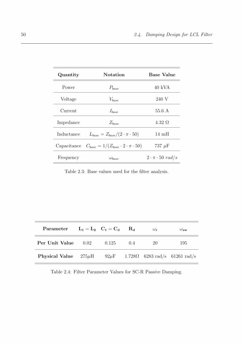
50 2.4. Damping Design for LCL Filter
Quantity Notation Base Value
Power Pbase 40 kVA
Voltage Vbase 240 V
Current Ibase 55.6 A
Impedance Zbase 4.32 Ω
Inductance Lbase = Zbase/(2 · π · 50) 14 mH
Capacitance Cbase = 1/(Zbase · 2 · π · 50) 737 µF
Frequency ωbase 2 · π · 50 rad/s
Table 2.3: Base values used for the filter analysis.
Parameter L1 = L2 C1 = Cd Rd ωr ωsw
Per Unit Value 0.02 0.125 0.4 20 195
Physical Value 275µH 92µF 1.728Ω 6283 rad/s 61261 rad/s
Table 2.4: Filter Parameter Values for SC-R Passive Damping.

Chapter 2. LCL Filter Design 51
01
23
45
02468
10
12
a
MinimumQualityFactor
C
Fig
ure
2.11
:V
aria
tion
ofm
inim
um
QF
wit
haC
=Cd/C
1in
cludin
gth
eeff
ect
ofre
sonan
cefr
equen
cysh
ift.
The
plo
tuse
s
ωr
=√ωfu·ω
sw,
rate
d3-
phas
ep
ower
(pow
erbas
e)of
250
kV
Afo
rth
ein
vert
eran
dnom
inal
grid
volt
age
(vol
tage
bas
e,
freq
uen
cybas
e)=
240
V,
50H
z.T
he
min
imum
qual
ity
fact
orcu
rve
does
not
chan
gew
ith
swit
chin
gfr
equen
cy.

52 2.4. Damping Design for LCL Filter
01
23
45
0
0.02
0.04
0.06
0.08
0.1
0.12
0.14
a
TotalPowerLoss(p.u)
fsw=2.25kHz
fsw=4.75kHz
fsw=7.25kHz
fsw=9.75kHz
C
Fig
ure
2.12
:V
aria
tion
ofPT
wit
haC
=Cd/C
1fo
rva
ryin
gva
lues
ofsw
itch
ing
freq
uen
cy.
The
plo
tuse
sωr
=√ωfu·ω
sw,
inve
rter
rate
d3-
phas
ep
ower
(pow
erbas
e)=
250
kV
Aan
dnom
inal
grid
volt
age
(vol
tage
bas
e,fr
equen
cybas
e)=
240
V,
50H
z.

Chapter 2. LCL Filter Design 53
damping component selection method provided above. This also explains the QF curve in
Fig. 2.11 remaining the same for varying switching and resonance frequencies.
Fig. 2.13 shows the pole-zero plot for a SC-R damped LCL filter with C1 = Cd and
Rd varying from 0.5√L/C to 10
√L/C. It can be observed that the system has maximum
damping when Rd is around√L/C. The solid arrows in the figure indicate the poles and
zeros corresponding to the component selection C1 = Cd and Rd =√L/C.
Pole-Zero Map
Imagin
ary
Axis
Real Axis
0.72 0.58 0.4 0.20.830.91
0.96
0.99
2e+04 1.5e+04 1e+04 5e+03
0.72 0.58 0.4 0.20.830.91
0.96
0.99
-2.5 -2 -1.5 -1 -0.5 0
0.8
0.6
0.4
0.2
0
-0.2
-0.4
-0.6
-0.8
-1
1
Pole
Pole
Pole
Zero
Pole
Zer
o
Figure 2.13: Pole-Zero plot of SC-R damped LCL filter for varying Rd. Rd is varied from
0.5√L/C to 10
√L/C. The system has maximum damping when Rd is around
√L/C. The
dashed arrows indicate pole movement for increasing Rd. The solid arrows indicate poles
and zeros for the component selection C1 = Cd and Rd =√L/C.

54 2.4. Damping Design for LCL Filter
2.4.4.3 Selection of Ld for SC-RL Damping Scheme
The QF and PT are the determining factors for selection of Ld also. As indicated in Sec-
tion 2.4.2.2, KLd= ωr/ωfu = ωr(p.u) = 20 gives the minimum QF. Using the expressions
(32) - (34), power loss can be plotted as a function of damping impedance factor KLdas
shown in Fig. 2.14. The power loss curve shows that KLd= 20 is a good choice in terms of
PT also. This suggests a relationship between KLdand ωr.
The choice of KLd= 20 assumes that the resonance frequency does not vary after the
ideal LCL filter is modified to include the passive damping components. So, the value of KLd
is tuned numerically to capture the effect of the shift in the resonance frequency. To tune
the value of KLdnumerically, a bode plot of the transfer function VC/Vi given by (26) was
plotted for KLd= 1 to 30. From the peaks of the bode plots computed numerically for KLd
= 1 to 30, an exact plot of quality factor as a function of damping impedance factor KLdis
obtained and is shown in Fig. 2.15. A numerical approach by plotting the exact bode gain
plots is used because an analytical solution would need solving a fifth order characteristic
equation.
The plot shows the tuned value of KLdthat gives the lowest QF to be 10.5 including the
effect of shift in the resonance frequency due to the addition of the damping components.
Fig. 2.14, KLd= 10.5 is suitable in terms of PT also. The choice of KLd
= 10.5 yields the
value of the damping inductor, Ld = 0.04 p.u. All the computations being in per-unit, the
value arrived at is valid for converters for a wide range of power rating and switching at
9.75 kHz with resonance frequency being set at 1 kHz. The proposed component selection
method for SC-RL damping scheme is useful for the power range of a few tens of kVA to
around 1 MVA. At higher power levels, it might not be possible to switch the inverter at
9.75 kHz. The effect of use of lower switching frequencies is considered in the next Section.
2.4.4.4 Damping Impedance Factor (KLd) - Physical Implication and Some Ob-
servations
The damping impedance factor is,
KLd=
Rd
ωfu · Ld(47)
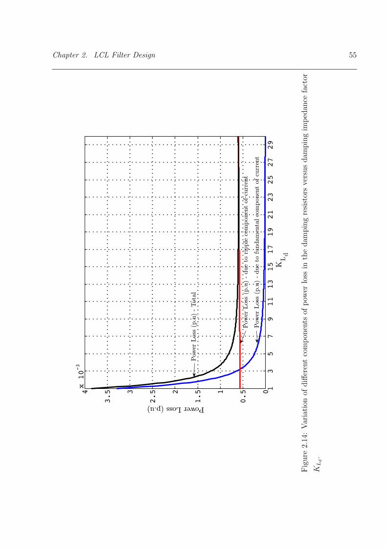
Chapter 2. LCL Filter Design 55
13
57
911
13
15
17
19
21
23
25
27
29
0
0.51
1.52
2.53
3.54x10⁻³
PowerLoss(p.u)
K
PowerLoss(p.u)-Total
PowerLoss(p.u)-duetofundamentalcomponentofcurrent
PowerLoss(p.u)-duetoripplecomponentofcurrent
Ld
Fig
ure
2.14
:V
aria
tion
ofdiff
eren
tco
mp
onen
tsof
pow
erlo
ssin
the
dam
pin
gre
sist
ors
vers
us
dam
pin
gim
ped
ance
fact
or
KLd.

56 2.4. Damping Design for LCL Filter
05
10
15
20
25
30
2
2.53
3.54
4.55
K
Qualityfactor
Ld
Fig
ure
2.15
:Q
Fdet
erm
ined
num
eric
ally
from
the
mag
nit
ude
bode
plo
tve
rsus
dam
pin
gim
ped
ance
fact
orKLd
incl
udin
g
the
effec
tof
reso
nan
cefr
equen
cysh
ift.

Chapter 2. LCL Filter Design 57
The physical implication of varying KLdis that it changes the impedance offered at
resonance frequency by the parallel combination of Rd and Ld. For example, a choice of KLd
= ωr/ωfu means that the impedance of Ld equals the value of Rd at ωr. Thus the effective
impedance at ωr is Rd/2. As KLddecreases, the effective impedance at ωr moves close to
Rd which is desirable. But, the value of KLdcannot be reduced arbitrarily as it would soon
lead to an increase in the fundamental frequency losses as can be observed from Fig. 2.14.
Also, QF does not vary linearly with KLdwhich can be observed from Fig 2.15.
It is numerically observed that KLdcan practically be chosen to be,
KLd=
1
2· ωrωfu
(48)
The value of KLdthat gives the minimum QF and low PT is observed to be close to (48)
and can be approximated to it. This has been seen to hold good for a wide range of switching
frequencies and wide choice of inductance and capacitance values. Fig. 2.16 and Fig. 2.17
plot QF vs KLdand PT vs KLd
respectively for switching frequencies in the range 2 kHz to
10 kHz. It can be seen that with KLdchosen using (48), the QF is very close to minimum
and power loss does not exceed the knee point of the curve. This can readily be applied to
inverters of power level up to around 1 MW and operating at switching frequencies in the
range 2 kHz to 10 kHz with voltage drop across the inductors (L1 + L2) ranging from 4%
to 17.5%.
The minimum QF obtained using the choice of KLdgiven by (48) can be reasoned out
using the pole zero plot. The SC-RL damped LCL filter has five poles. Apart from the one
pole at origin, the other four poles can be two sets of complex conjugates or a set of complex
conjugates and a set of real poles. For the suggested choice of KLdgiven by (48) and other
parameters as in Section 2.4.4.2, the four poles turn out to be two sets of complex conjugates
that are equal given by s = ωr[−(1/2)± (√
3/2)] – twin poles at each location. These poles
always lie along a constant damping line irrespective of the choice of resonance and switching
frequency. Also, the zeros of (26) can also be shown to always lie along constant damping
lines. This leads to a fixed and minimum quality factor as can be observed from Fig. 2.16.
So, the validity of the design is based only on PT curve. As far as the suggested value of KLd
is at or below the knee of the PT curve, the power loss does not become excessive and the
design holds good. For switching frequencies from 2 kHz and above, the suggested KLdvalue
is at or below the knee point of the PT curve as shown in Fig. 2.17 and hence results in a valid
design. Further, the twin complex conjugate poles indicate that the additional resonance

58 2.4. Damping Design for LCL Filter
12
34
56
78
910
11
2
2.53
3.54
4.55
5.56
K
ExactQualityFactor
ωfur
ω0.5x
fsw=4.75kHz
fsw=7.25kHz
fsw=2.25kHz
Ld
fsw=9.75kHz
Fig
ure
2.16
:V
aria
tion
ofQ
Fw
ithKLd
incl
udin
gth
eeff
ect
ofre
sonan
cefr
equen
cysh
ift
for
vary
ing
valu
esof
swit
chin
g
freq
uen
cy.
The
plo
tuse
sωr
=√ωfu·ω
sw,
inve
rter
rate
d3-
phas
ep
ower
(pow
erbas
e)=
250
kV
Aan
dnom
inal
grid
volt
age
(vol
tage
bas
e,fr
equen
cybas
e)=
240
V,
50H
z.

Chapter 2. LCL Filter Design 59
12
34
56
78
910
11
12
13
14
15
0
0.002
0.004
0.006
0.008
0.01
0.012
0.014
0.016
0.018
0.02
0.022
0.024
K
TotalPowerLoss(p.u)
Ld
ω ωfur
fsw=9.75kHz
fsw=4.75kHz
fsw=7.25kHz
fsw=2.25kHz
0.5x
Fig
ure
2.17
:V
aria
tion
ofPT
wit
hKLd
for
vary
ing
valu
esof
swit
chin
gfr
equen
cy.
The
plo
tuse
sωr
=√ωfu·ω
sw,
inve
rter
rate
d3-
phas
ep
ower
(pow
erbas
e)=
250
kV
Aan
dnom
inal
grid
volt
age
(vol
tage
bas
e,fr
equen
cybas
e)=
240
V,
50H
z.
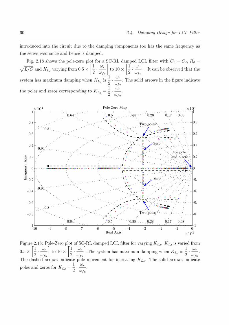
60 2.4. Damping Design for LCL Filter
introduced into the circuit due to the damping components too has the same frequency as
the series resonance and hence is damped.
Fig. 2.18 shows the pole-zero plot for a SC-RL damped LCL filter with C1 = Cd, Rd =√L/C and KLd
varying from 0.5×[
1
2· ωrωfu
]to 10×
[1
2· ωrωfu
]. It can be observed that the
system has maximum damping when KLdis
1
2· ωrωfu
. The solid arrows in the figure indicate
the poles and zeros corresponding to KLd=
1
2· ωrωfu
.
Real Axis
Imagin
ary
Axis
Pole-Zero Map
0.2
0.4
0.6
0.8
1
-0.2
-0.4
-0.6
-0.8
-1-10 -9 -8 -7 -6 -5 -4 -3 -2 -1 0
0.080.170.280.380.50.64
0.8
0.94
0.080.170.280.380.50.64
0.8
0.94
0
0.2
0.4
0.6
0.8
1
-0.2
-0.4
-0.6
-0.8
-1
0
Two poles
One pole
and a zero
Two poles
Zero
Zero
Figure 2.18: Pole-Zero plot of SC-RL damped LCL filter for varying KLd. KLd
is varied from
0.5×[
1
2· ωrωfu
]to 10×
[1
2· ωrωfu
].The system has maximum damping when KLd
is1
2· ωrωfu
.
The dashed arrows indicate pole movement for increasing KLd. The solid arrows indicate
poles and zeros for KLd=
1
2· ωrωfu
.

Chapter 2. LCL Filter Design 61
2.4.5 Summary of Component Selection Procedure for an SC-RL
Damped LCL Filter
The following steps summarize the selection procedure for the various components of an
output SC-RL damped LCL filter in a grid-connected inverter. The system is assumed to
be connected in a 3-phase 4-wire configuration.
1. Select a desired ωsw based on the device restrictions and thermal considerations. A
ωsw that does not result in even harmonics in the output voltage spectrum can reduce
the minimum value of inductance required.
2. Choose a resonance frequency, ωr which is well separated from both ωfu and ωsw.
Ideally, ωr can be chosen to be, ωr =√ωfu · ωsw . However, a slightly higher value of
ωr might be used to reduce the system size and cost.
3. Compute Lmin1(p.u.) using the relation, Lmin1 =|Vi(ωdom)|
|Ig(ωdom)| |ωdom| |1− (ωdom/ωr)2|
.
This is required for the ideal LCL filter without the damping components to comply
with the IEEE standards.
4. Lmax = 0.1 p.u. This is required for a practical choice of dc bus voltage.
5. L1 = L2 = L/2 from the inductor cost perspective. L2 includes the grid inductance.
6. Choose a value of Cmax based on the desired limit on the reactive power requirement
of the filter capacitor.
7. Lmin2 =4
ω2rCmax
.
8. Choose any value of L that satisfies, max(Lmin1, Lmin2) ≤ L ≤ Lmax.
9. C =4
ω2rL
.
10. C1 = Cd = C/2 and Rd =√L/C. This selection of C1, Cd and Rd gives a low value of
QF and PT in an SC-R damped LCL filter.
11. KLd=
1
2· ωrωfu
for QF and PT to be very low in a SC-RL damped LCL filter. Corre-
spondingly, Ld =Rd
KLd· ωfu
or Ld = L1 + L2 = L.
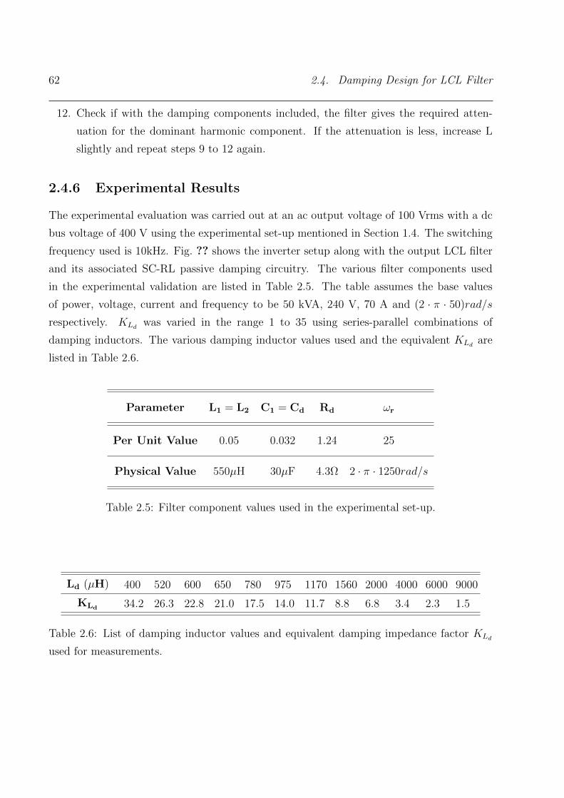
62 2.4. Damping Design for LCL Filter
12. Check if with the damping components included, the filter gives the required atten-
uation for the dominant harmonic component. If the attenuation is less, increase L
slightly and repeat steps 9 to 12 again.
2.4.6 Experimental Results
The experimental evaluation was carried out at an ac output voltage of 100 Vrms with a dc
bus voltage of 400 V using the experimental set-up mentioned in Section 1.4. The switching
frequency used is 10kHz. Fig. ?? shows the inverter setup along with the output LCL filter
and its associated SC-RL passive damping circuitry. The various filter components used
in the experimental validation are listed in Table 2.5. The table assumes the base values
of power, voltage, current and frequency to be 50 kVA, 240 V, 70 A and (2 · π · 50)rad/s
respectively. KLdwas varied in the range 1 to 35 using series-parallel combinations of
damping inductors. The various damping inductor values used and the equivalent KLdare
listed in Table 2.6.
Parameter L1 = L2 C1 = Cd Rd ωr
Per Unit Value 0.05 0.032 1.24 25
Physical Value 550µH 30µF 4.3Ω 2 · π · 1250rad/s
Table 2.5: Filter component values used in the experimental set-up.
Ld (µH) 400 520 600 650 780 975 1170 1560 2000 4000 6000 9000
KLd 34.2 26.3 22.8 21.0 17.5 14.0 11.7 8.8 6.8 3.4 2.3 1.5
Table 2.6: List of damping inductor values and equivalent damping impedance factor KLd
used for measurements.
Chapter 2. LCL Filter Design 63
0 4 8 12 16 20 24 28 32 352
2.5
3
3.5
4
4.5
Damping Impedance Factor (K
QualityFactor(Q)
Experimental
Theoretical
dL )
Figure 2.19: Theoretical and experimental quality factor curves as a function of the damping
impedance factor KLd.
2.4.6.1 Measurement of QF
A network analyser (AP Instruments - Model 200) is used to experimentally determine the
quality factors for various values of KLd. Fig. 2.19 shows the theoretical and experimental
quality factor curves. The deviations in the quality factor from the theoretical values can
be attributed to the component tolerances and the non-idealities associated with the circuit
elements. In particular, it can be observed that the experimental curve shows the damping to
have improved over the theoretical prediction which is expected as the ESR of the inductor
and capacitor and the wire resistances give additional damping.
2.4.6.2 Measurement of Power Loss (Pfu and Pri)
To experimentally validate the fundamental frequency power loss Pfu in the filter damping
resistor, the inverter should be connected to the grid through the SC-RL damped LCL filter.

64 2.4. Damping Design for LCL Filter
Equivalently, the current circulation procedure developed in Chapter 3 can also be used as
only the fundamental frequency component of current in the damping resistor is of interest.
Hence, the current circulation procedure is used in the present work. A digital power meter
(Yokogawa - WT1600) is used to experimentally measure the power loss due to fundamental
frequency component of current through the damping resistor (Rd).
The worst case ripple current power loss is to be calculated at a duty ratio of d = 0.5. To
experimentally validate the power loss in the damping resistor due to the worst case ripple
current Pri, the grid is shorted i.e. the grid is disconnected and the grid-side inductors are
connected to mid-point of the dc bus capacitor. Then, a 50% duty cycle pulse is applied at
the output of the inverter and the loss due to the worst case ripple current in the damping
resistor is measured using the data of current from high bandwidth LEM current sensors
captured through LeCroy WaveRunner 6050 oscilloscope.
0 4 8 12 16 20 24 28 32 350
0.25
0.5
0.75
1
1.25
1.5
1.75
2x 10⁻⁴
Damping Impedance Factor (K
Power
Loss
(p.u.)
Total power loss - Experimental
Total power loss - Theoretical
Power loss due to worst-case switching ripple current - Theoretical
Power loss due to worst-case switching ripple current - Experimental
Power loss at fundamental frequency - Experimental
Power loss at fundamental frequency - Theoretical
dL)
Figure 2.20: Theoretical and experimental power loss comparison as a function of the damp-
ing impedance factor KLd. Curves for the fundamental loss component, switching loss com-
ponent and total loss are indicated.
Chapter 2. LCL Filter Design 65
Figure 2.21: Operation of the inverter with LCL filter at an output of 100 V (rms), 40 A
(rms) at unity power factor. Ch1: Inverter-side inductor current (100 A/div); Ch2: Grid-side
inductor current (100 A/div); Ch3: voltage across capacitor Vc (100 V/div).
Fig. 2.20 shows the theoretical and experimental power loss curves for fundamental com-
ponent, ripple component and the total power loss. The experimental power loss curves
closely match the values from the theoretical analysis for both fundamental and switching
frequency components. As suggested in Section 2.4.4.4, a selection of KLd= 12.5 based
on (48) is a good choice in terms of QF and PT as observed from Fig. 2.19 and Fig. 2.20
respectively.
Fig. 2.21 shows the inverter-side inductor current, filtered grid-side inductor current and
output filter capacitor voltage, vC . The waveform was captured with the inverter giving a
sinusoidal output of 100V rms at unity power factor and carrying a line current of 40A. The
damping inductor used was 390µH.
2.4.6.3 Filtering Performance
Fig. 2.22(a) and Fig. 2.23(a) show the inverter-side inductor current, filtered grid-side in-
ductor current and output filter capacitor voltage, vC without and with the passive damping
circuitry respectively. The waveforms have been captured with the inverter giving a sinu-
soidal output of 100 V and unity power factor at the inverter output terminals. The line
current is 40 A. In the case of damped LCL filter, the damping inductor used was 1.17 mH

66 2.4. Damping Design for LCL Filter
(a)
0 2.5 5 7.5 10 12.5 15 17.5 20 22.5 25−20
0
20
40
Frequency in kHz
MagnitudeindB
0 2.5 5 7.5 10 12.5 15 17.5 20 22.5 25
-20
0
20
40
Frequency in kHz
MagnitudeindB
0 2.5 5 7.5 10 12.5 15 17.5 20 22.5 25
-20
0
20
40
Frequency in kHz
MagnitudeindB
Voltage across filter capacitor
Grid side inductor current
Inverter side inductor current
Presence of resonance frequency component
Undamped resonance frequency component
Switching frequency components
(b)
Figure 2.22: Power converter waveforms and spectrum at an output of 100 V (rms), 40 A
(rms) and unity power factor at the inverter output terminal without the SC-RL passive
damping circuitry. (a) Operation of the inverter with undamped LCL filter. Ch1: Grid-side
inductor current (100 A/div); Ch2: Inverter-side inductor current (100 A/div); Ch4: voltage
across capacitor Vc (100 V/div). (b) Spectrum of waveforms in (a).
Chapter 2. LCL Filter Design 67
(a)
0 2.5 5 7.5 10 12.5 15 17.5 20 22.5 25−2002040
Frequency in kHz
Magnitude(dB)
0 2.5 5 7.5 10 12.5 15 17.5 20 22.5 25
-20
0
20
40
Frequency in kHz
Magnitude(dB)
0 2.5 5 7.5 10 12.5 15 17.5 20 22.5 25
-20
0
20
40
Frequency in kHz
Magnitude(dB)
Inverter side inductor current
Grid side inductor current
Voltage across filter capacitor
Switching frequency components
Absence of resonance frequency component
Damped resonance frequency component
(b)
Figure 2.23: Power converter waveforms and spectrum at an output of 100 V (rms), 40
A (rms) and unity power factor at the inverter output terminal with the SC-RL passive
damping circuitry. (a) Operation of the inverter with damped LCL filter. Ch1: Grid-side
inductor current (100 A/div); Ch2: Inverter-side inductor current (100 A/div); Ch4: voltage
across capacitor Vc (100 V/div). (b) Spectrum of waveforms in (a).
68 2.5. Summary
which gives very low QF as shown in Fig. 2.19 corresponding to KLd= 11.7.
Fig. 2.22(b) and Fig. 2.23(b) show the FFT spectrum of the waveforms in Fig. 2.22(a)
and Fig. 2.23(a) respectively. The FFT spectrums show the filtering performance of the LCL
filter and the effect of the passive damping circuitry at the resonance frequency. With damp-
ing, the grid side current ripple is 0.085 A and the inverter side current ripple is 4.01 A at the
switching frequency. The corresponding filter attenuation (ig/vi) at the switching frequency
is -64.25 dB. The experimentally obtained attenuation is close to the analytically computed
attenuation of -66.8 dB. The capacitor voltage has oscillations of magnitude 2.58 V at the
resonance frequency without damping. With the SC-RL damping network, the magnitude is
reduced to 0.28 V. The rms switching ripple current in the damping resistor analytically ob-
tained under the mentioned operating conditions is 0.484 A. The experimental measurement
is 0.479 A which has an error of 1.03%.
2.5 Summary
A detailed study of LCL filter design with specific emphasis on passive damping network de-
sign has been presented. SC-RL passive damping is the passive damping network considered
for the study. The SC-RL damped LCL filter has been modelled using state space approach.
Using this model, expressions have been derived for quality factor and total power loss in the
damping resistor. The expressions are used to show the lower total power loss in the damping
resistors in the SC-RL damping method as compared to the purely resistive damping and
SC-R damping cases. This makes the SC-RL damping a good choice of LCL filter damping
method for high power inverters connected to the grid. Also, the normalised quantitative
total power loss evaluated for the same level of damping is useful for the designers to make
a choice on the passive damping method that can be employed.
A procedure for SC-RL damping circuit design has been proposed with the intent of
keeping the QF low in the range of 2.0 to 2.5 and while maintaining the total power loss in the
damping resistor to be in the range of 0.05% to 0.1%. The trade-off involved in systematically
designing the passive damping circuit, with choice for C1, Cd and Rd, is provided. A damping
impedance factor, KLd, has been introduced in the process of developing the design procedure
and is used to select Ld. An expression for a suitable value of KLdis provided. This value of
KLdis shown to give a low quality factor along with low losses in the damping resistors. This
is verified analytically over a wide range of switching frequencies, power levels and choice

Chapter 2. LCL Filter Design 69
of inductance and capacitance values of the filter. The outlined method is useful for high
power inverters connected to the grid. Experimental measurements were made using a large
number of inductors to vary KLdfor practical evaluation of its impact on the filter damping
performance. The filter was used in a power converter at an output of 100 Vrms, 40 Arms,
50 Hz and the filtering performance closely matched the analysis.

70 2.5. Summary

Chapter 3
Thermal Performance Evaluation of
High Power Grid-Connected Inverters
For improved reliability, it is desirable to evaluate the thermal performance of grid-connected
inverters at their rated operating conditions. It is particularly useful in the present day sce-
nario where power levels of grid-connected inverters have increased to MW range. With
this motivation, a novel test method to test high power grid-connected inverters has been
developed. In an inverter, the semiconductor devices are prone to frequent failures compared
to the associated passive components. So, thermal performance evaluation generally focuses
on the thermal testing of the semiconductor switches [82, 92] only. In the proposed method
too, the primary focus is on thermal testing of the semiconductor switches. However, the
method being developed for high power inverters, the thermal response of the output filter
inductors, the dc bus capacitors and the output filter capacitors also need attention. While
high temperatures can lead to insulation failure in inductors, the operating life of the capac-
itors depend on the thermal effects of the current through them [16]. So, the usefulness of
the proposed method to test the dc bus capacitors and output filter inductors and capacitors
has also been studied.
This Chapter discusses the thermal test method in detail. In Section 3.1, the various
inverter testing methods available in literature are explained. Section 3.2 details the proposed
test method. Phasor analysis has been provided in Section 3.3 to get a better physical insight
into the operation of the proposed test method. In Section 3.4, Common Mode (CM) and
Differential Mode (DM) equivalent circuits are developed for the actual system and the
proposed test configuration. Section 3.5 uses the equivalent circuits to design the closed
loop control for the proposed test method. Section 3.6 gives the details of the hardware
configuration used to validate the method experimentally. In Section 3.7, the low frequency
71
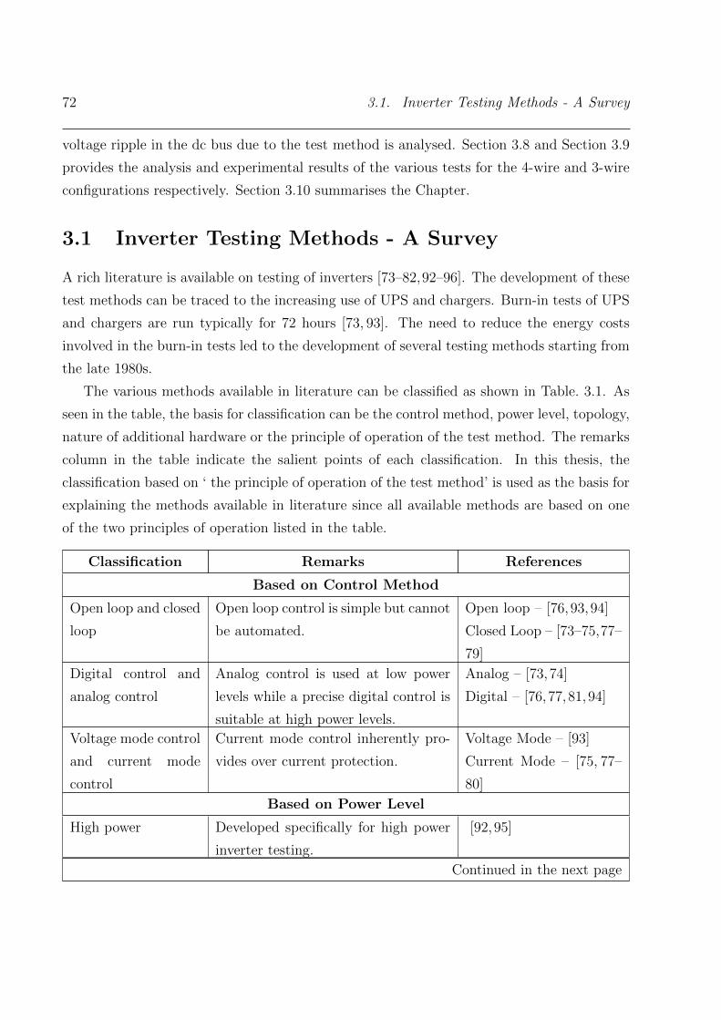
72 3.1. Inverter Testing Methods - A Survey
voltage ripple in the dc bus due to the test method is analysed. Section 3.8 and Section 3.9
provides the analysis and experimental results of the various tests for the 4-wire and 3-wire
configurations respectively. Section 3.10 summarises the Chapter.
3.1 Inverter Testing Methods - A Survey
A rich literature is available on testing of inverters [73–82,92–96]. The development of these
test methods can be traced to the increasing use of UPS and chargers. Burn-in tests of UPS
and chargers are run typically for 72 hours [73, 93]. The need to reduce the energy costs
involved in the burn-in tests led to the development of several testing methods starting from
the late 1980s.
The various methods available in literature can be classified as shown in Table. 3.1. As
seen in the table, the basis for classification can be the control method, power level, topology,
nature of additional hardware or the principle of operation of the test method. The remarks
column in the table indicate the salient points of each classification. In this thesis, the
classification based on ‘ the principle of operation of the test method’ is used as the basis for
explaining the methods available in literature since all available methods are based on one
of the two principles of operation listed in the table.
Classification Remarks References
Based on Control Method
Open loop and closed
loop
Open loop control is simple but cannot
be automated.
Open loop – [76,93,94]
Closed Loop – [73–75,77–
79]
Digital control and
analog control
Analog control is used at low power
levels while a precise digital control is
suitable at high power levels.
Analog – [73,74]
Digital – [76,77,81,94]
Voltage mode control
and current mode
control
Current mode control inherently pro-
vides over current protection.
Voltage Mode – [93]
Current Mode – [75, 77–
80]
Based on Power Level
High power Developed specifically for high power
inverter testing.
[92,95]
Continued in the next page
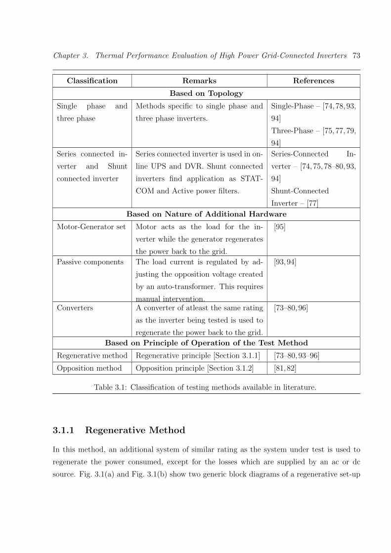
Chapter 3. Thermal Performance Evaluation of High Power Grid-Connected Inverters 73
Classification Remarks References
Based on Topology
Single phase and
three phase
Methods specific to single phase and
three phase inverters.
Single-Phase – [74,78,93,
94]
Three-Phase – [75, 77, 79,
94]
Series connected in-
verter and Shunt
connected inverter
Series connected inverter is used in on-
line UPS and DVR. Shunt connected
inverters find application as STAT-
COM and Active power filters.
Series-Connected In-
verter – [74, 75, 78–80, 93,
94]
Shunt-Connected
Inverter – [77]
Based on Nature of Additional Hardware
Motor-Generator set Motor acts as the load for the in-
verter while the generator regenerates
the power back to the grid.
[95]
Passive components The load current is regulated by ad-
justing the opposition voltage created
by an auto-transformer. This requires
manual intervention.
[93,94]
Converters A converter of atleast the same rating
as the inverter being tested is used to
regenerate the power back to the grid.
[73–80,96]
Based on Principle of Operation of the Test Method
Regenerative method Regenerative principle [Section 3.1.1] [73–80,93–96]
Opposition method Opposition principle [Section 3.1.2] [81,82]
Table 3.1: Classification of testing methods available in literature.
3.1.1 Regenerative Method
In this method, an additional system of similar rating as the system under test is used to
regenerate the power consumed, except for the losses which are supplied by an ac or dc
source. Fig. 3.1(a) and Fig. 3.1(b) show two generic block diagrams of a regenerative set-up
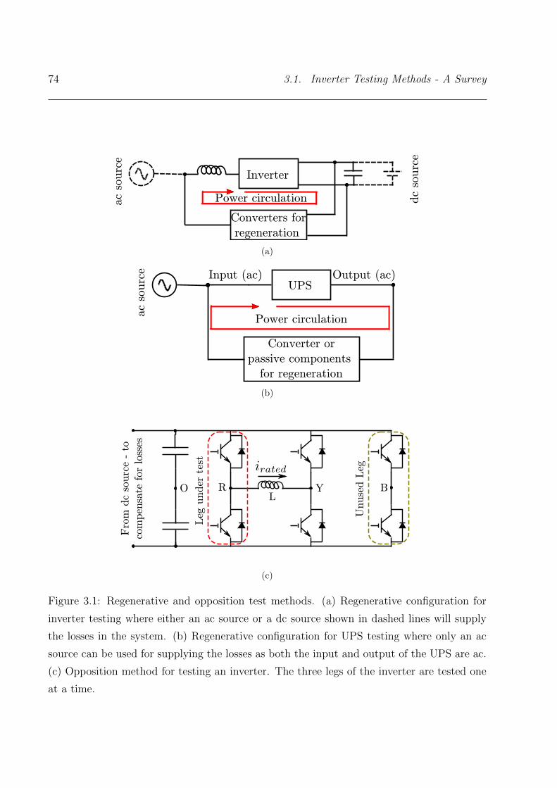
74 3.1. Inverter Testing Methods - A Survey
Inverter
Converters for
regeneration
ac
sourc
e
dc
sourc
e
Power circulation
(a)
UPS
Converter or
passive components
for regeneration
ac
sourc
e
Power circulation
Input (ac) Output (ac)
(b)
Fro
m d
c so
urc
e -
to
com
pen
sate
for
loss
es
O R Y B
Leg
under
tes
t
Unuse
d L
eg
(c)
Figure 3.1: Regenerative and opposition test methods. (a) Regenerative configuration for
inverter testing where either an ac source or a dc source shown in dashed lines will supply
the losses in the system. (b) Regenerative configuration for UPS testing where only an ac
source can be used for supplying the losses as both the input and output of the UPS are ac.
(c) Opposition method for testing an inverter. The three legs of the inverter are tested one
at a time.

Chapter 3. Thermal Performance Evaluation of High Power Grid-Connected Inverters 75
where the power circulates within the two systems - the inverter under test and the addi-
tional hardware used to regenerate the power. References [73–80,93–96] use the regenerative
method. References [93] and [94] suggest using simple passive components for regeneration.
References [73–80] all use additional converters for regeneration with differences in their
topology. References [73,74] and [76] achieve unity power factor (UPF) along with regener-
ation. References [95] and [96] discuss regenerative methods developed specifically for high
power inverters. While [95] uses a motor-generator set to regenerate power, [96] uses two
back-to-back connected inverters for regeneration.
The drawback of this method is that it requires additional systems – converters or passive
components – that are rated equal or higher than the system under test.
3.1.2 Opposition Method
In this method, one leg of the inverter is tested at a time. As shown in Fig. 3.1(c) an
inductive filter is connected between two legs of the inverter and the third leg is left unused.
First, rated voltage is set at the output of the leg under test. Then, the voltage at the output
of the other leg is adjusted to set a differential voltage that drives the rated current.
For example, let R-phase leg be the leg under test as shown in Fig. 3.1(c). Let the rated
voltage and rated current at its output for a given grid power factor angle, φ be represented
by the phasors V R,rated and IR,rated respectively. ‘φ’ is the angle between the voltage and
current at the point of common coupling with the grid. Then, first vR is set to V R,rated. So,
we have – assuming rated current to flow between R and Y phases,
VR = V R,rated = VY + ωL · IR,rated (49)
where, VR, VY are the voltage phasors of the voltages at R and Y with respect to dc bus
mid-point ‘O’ respectively.
From (49), to achieve rated current at the output of the R-phase leg, the Y-phase voltage
has to be,
VY = V R,rated − ωL · IR,rated (50)
From, (49) and (50), the common mode and differential mode components of voltages
can be found to be,

76 3.1. Inverter Testing Methods - A Survey
V cm = V R,rated −1
2· ωL · IR,rated (51)
V R,dm =1
2· ωL · IR,rated (52)
V Y,dm = −1
2· ωL · IR,rated (53)
By applying the common mode and differential mode voltages as given by (51), (52) and
(53), rated voltage and rated current can be obtained at the output of the leg under test at
a given grid power factor angle φ.
Since the load is an inductor, the power drawn from the source compensates only for
the semiconductor losses and the losses in the small resistance associated with the inductor.
Hence, the power drawn is minimal. References [81] and [82] use the opposition method.
As one leg is not switched at all during the test, with a common cooling arrangement, the
temperature rise in the heatsink over ambient will not match that of the actual system where
all three legs are switching. So, this method can be used only when the three legs of the
inverter have independent cooling arrangement. Apart from the regenerative and opposition
methods, [92] explores the use of series-resonance principle for inverter testing.
From the above discussion, it can be seen that all regenerative methods require passive
components [93,94] or converters [73–80,95,96] of similar or higher rating than the inverter
under test. This may suit testing of low power mass-produced inverters but can be imprac-
tical for high power converters, especially the ones that are custom built. The opposition
method, also known as the two leg test [81,82], and the series resonant approach [92] are the
two available self-test methods that do not require additional systems of similar or higher
power rating as the inverter under test. However, the usefulness of the opposition method
and series-resonance approach are limited to systems where each leg is mounted on a sep-
arate heatsink or where the thermal cooling loop for each phase leg is independent. Also,
like the regenerative methods discussed in Section 3.1.1, these have been developed only for
thermal testing of the semiconductor devices. The possibility of using the methods to test
the dc bus capacitors and output filter components has not been studied.

Chapter 3. Thermal Performance Evaluation of High Power Grid-Connected Inverters 77
3.1.3 Focus of Work
The test method proposed in this thesis aims at addressing the issues in the methods available
in literature while retaining their advantages. The focus of the work can be listed as given
below:
1. To develop a test method that can evaluate the thermal performance of the semicon-
ductor switches.
2. To ensure that the proposed method meets the following requirements:
• It does not require high power source or load. Only the losses in the system is
required to be supplied during the test.
• It does not require any additional converters or passive components of high power
for power circulation.
• It can be used in either case of the IGBT modules mounted on a common heatsink
or separate individual heatsinks.
• It can be used for testing of both three-phase 4-wire and three-phase 3-wire sys-
tems. This would make it useful for a wide variety of PWM techniques.
• It can be used without significant changes in the hardware.
3. To study the usefulness of the proposed method to evaluate the thermal performance
of the dc bus capacitors and the output filter components.
3.2 Proposed Test Method
3.2.1 Actual System and Test Configuration
Fig. 3.2(a) shows the actual system to be tested - a generic high power three-phase grid-
connected inverter. An LCL filter is considered at the output as it is generally required [33,89]
to meet the IEEE standards [28, 65] for grid-connection. Both 3-wire connection shown in
solid lines and 4-wire connection shown in dashed lines are possible. The configuration shown
represents a wide range of practical systems such as a DSTATCOM, shunt active filter, front-
end converter, inverter interfacing a distributed source with the grid and the like. In case of
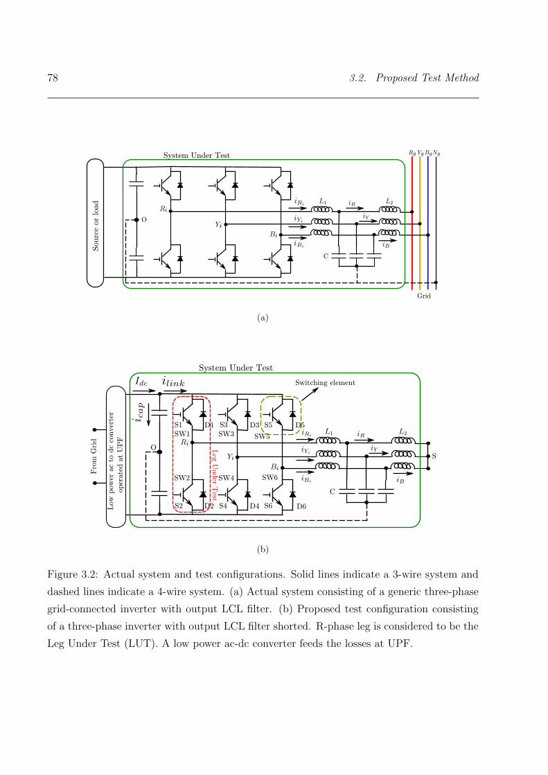
78 3.2. Proposed Test Method
Grid
Sourc
e or
load
System Under Test
O
C
(a)
L
ow
pow
er a
c to
dc
conver
ter
oper
ate
d a
t U
PF
Fro
m G
rid
S1
S2
S3
S4
S5
S6
D1
D2
D3
D4
D5
D6
SW1
SW2
SW3
SW4
SW5
SW6
Switching element
System Under Test
C
Leg
Under T
est
SO
(b)
Figure 3.2: Actual system and test configurations. Solid lines indicate a 3-wire system and
dashed lines indicate a 4-wire system. (a) Actual system consisting of a generic three-phase
grid-connected inverter with output LCL filter. (b) Proposed test configuration consisting
of a three-phase inverter with output LCL filter shorted. R-phase leg is considered to be the
Leg Under Test (LUT). A low power ac-dc converter feeds the losses at UPF.
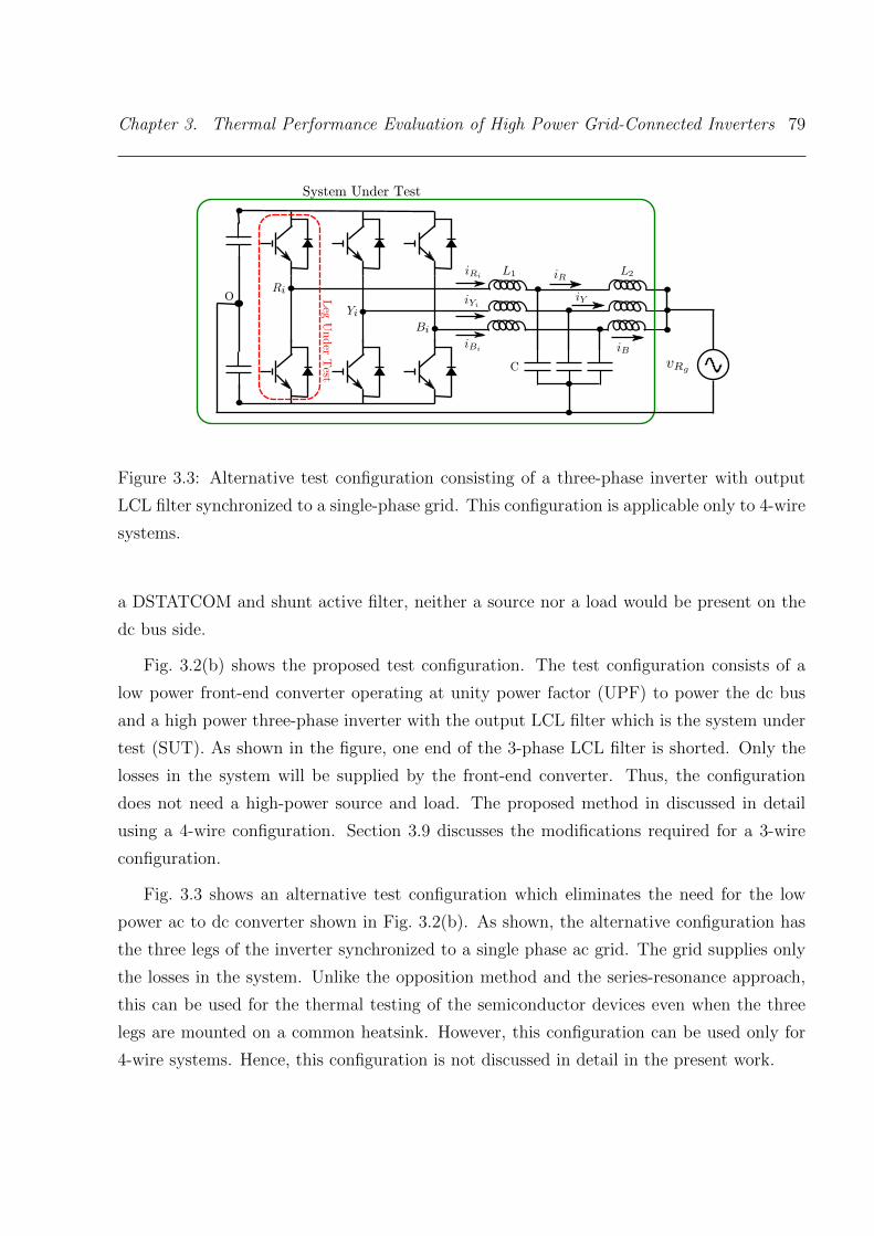
Chapter 3. Thermal Performance Evaluation of High Power Grid-Connected Inverters 79
System Under Test
C
Leg
Under T
est
O
Figure 3.3: Alternative test configuration consisting of a three-phase inverter with output
LCL filter synchronized to a single-phase grid. This configuration is applicable only to 4-wire
systems.
a DSTATCOM and shunt active filter, neither a source nor a load would be present on the
dc bus side.
Fig. 3.2(b) shows the proposed test configuration. The test configuration consists of a
low power front-end converter operating at unity power factor (UPF) to power the dc bus
and a high power three-phase inverter with the output LCL filter which is the system under
test (SUT). As shown in the figure, one end of the 3-phase LCL filter is shorted. Only the
losses in the system will be supplied by the front-end converter. Thus, the configuration
does not need a high-power source and load. The proposed method in discussed in detail
using a 4-wire configuration. Section 3.9 discusses the modifications required for a 3-wire
configuration.
Fig. 3.3 shows an alternative test configuration which eliminates the need for the low
power ac to dc converter shown in Fig. 3.2(b). As shown, the alternative configuration has
the three legs of the inverter synchronized to a single phase ac grid. The grid supplies only
the losses in the system. Unlike the opposition method and the series-resonance approach,
this can be used for the thermal testing of the semiconductor devices even when the three
legs are mounted on a common heatsink. However, this configuration can be used only for
4-wire systems. Hence, this configuration is not discussed in detail in the present work.

80 3.2. Proposed Test Method
3.2.2 Test Method
In the proposed method, each leg of the three-phase inverter is tested one at a time. Fig. 3.4
represents the equivalent circuit of the test configuration shown in Fig. 3.2(b) under the
proposed method of operation. As shown in the figure, the Leg Under Test (LUT) is operated
as an open loop voltage source and the other two legs are operated in closed loop current
control mode. Since the LCL filters are shorted at one end as shown in Fig. 3.2(b) and the
LCL filter capacitors draw only a small amount of current at the fundamental frequency, the
current through the LUT is almost the sum of the currents through the current controlled
legs. Thus, by appropriate choice of open loop voltage and closed loop currents, rated
terminal voltage and rated current can be set at the LUT, thus emulating that leg of the
actual system. Detailed test procedures for thermal testing of semiconductor devices, dc bus
capacitors and output filter components appear in Sections 3.8 and 3.9.
The alternative method shown in Fig. 3.3 also tests one leg at a time. Here, the synchro-
nization with the single phase grid ensures rated voltage at the output of the LUT. All the
three legs are current controlled to get a set of balanced rated currents. An outer dc bus
voltage control loop is used to draw a small in-phase current from the single phase mains to
supply the losses in the inverter.
LUT
SO
Figure 3.4: Equivalent circuit of test configuration under proposed method of operation.
LR1, LY 1 and LB1 represent the inverter-side output inductors of the three phases, LR2, LY 2
and LB2 represent the grid-side output inductors of the three phases and CR, CY and CB
represent the output filter capacitors of the three phases.

Chapter 3. Thermal Performance Evaluation of High Power Grid-Connected Inverters 81
3.2.3 Choice of Current References
From Fig. 3.4,
iR(t) = −(iY (t) + iB(t)) (54)
From (54), by forcing iY and iB to follow appropriately set current references, iR can be
controlled to be the same as in the actual system. There are theoretically infinite possible
combinations of iY and iB that give the required iR. In the proposed method, iY and iB are
chosen so as to form a three-phase balanced system of currents with iR. As can be seen in
Section 3.8.2, this selection of currents help in semiconductor device thermal test even when
the power semiconductor devices or modules are mounted on a common heatsink. Also,
from Section 3.8.3, this particular selection of current references can be seen to be useful
for the testing of dc bus capacitors. It may be noted that the two-leg test [81, 82] shown in
Fig. 3.1(c) is a particular case of the proposed test method with iB = 0 and iY = −iR. So,
the proposed test method can be viewed as a ‘generalized opposition method’.
3.3 Phasor Analysis
Let, VRg , VYg , VBg , VRi, VYi
, VBiand VS represent the fundamental frequency voltage
phasors at the respective nodes Rg, Yg, Bg, Ri, Yi, Bi and S with respect to the dc bus mid-
point O in Fig. 3.2(a) and Fig. 3.2(b). Further, let VLR, VLY
and VLBbe the fundamental
frequency phasors representing the phasor sum of the voltage drops across the two output
filter inductors in R, Y and B phase respectively.
Then, from Fig. 3.2(a), we have for the actual system,
VRi= VRg + VLR
(55)
And, from Fig. 3.2(b), we have for the test configuration,
VRi= VS + VLR
(56)
Similar phasor expressions can be written for the other legs of the actual system and the
test configuration. In the test configuration, to achieve the same voltage as the actual system
at the inverter output terminal of the LUT, VS is made equal to the grid-side voltage of the
LUT in the actual system. For example, when R-phase leg is the LUT, VS is set to VRg , so

82 3.3. Phasor Analysis
(a)
=
(b)
Figure 3.5: Phasor representations corresponding to the fundamental frequency when R-
phase is the LUT. (a) For the actual system. (b) For the proposed test configuration. The
phasor diagram has been drawn for a lagging grid power factor angle of 30o. The small
fundamental frequency current through the output filter capacitors has been neglected in
drawing this phasor diagram.
Chapter 3. Thermal Performance Evaluation of High Power Grid-Connected Inverters 83
that the test configuration represented by (56) is identical to the actual system represented
by (55). VS = VRg is a common mode voltage.
Fig. 3.5 shows the fundamental frequency phasor representation of the actual system and
the test configuration. Vectors corresponding to VLR, VLY
and VLBhave been shown greater
in magnitude than they actually are, for the sake of clarity of the diagrams. Their magnitudes
are typically around 10% of the grid voltage magnitude at the rated current [33, 89]. The
fundamental frequency component of current through the output LCL filter capacitors is
small and has not been included in these phasor diagrams. Fig. 3.5 is used to get better
physical understanding of the actual and test circuits. It may be noted that the fundamental
frequency current through the output filter capacitors depend on the nominal fundamental
frequency grid voltage and the LCL filter capacitance. It does not depend directly on the
power level. The only influence of power level comes through the chosen value of capacitance
as the capacitor value varies with the power level. For, the range of switching frequencies
and resonant frequencies considered in this thesis, the fundamental frequency component of
current is usually negligible. Also, though it has been neglected in the phasor analysis, it
has been included in the experiments by computing the current through the capacitor at
fundamental frequency and adding the same vectorially with the set reference current for
more accuracy.
In Fig. 3.5, the phasor diagrams have been drawn for a lagging grid power factor angle of
30o when R-phase is the LUT. As the grid current phase angle varies, the three-phase grid
currents trace the circumference of the bigger circle and the inverter terminal voltages trace
the circumference of the smaller circles in the figure.
3.3.1 Operation of the Actual System and Test Configuration – A
Physical Insight
In the actual system, the three-phase grid voltages (vRg , vYg , vBg) appear on the grid side
of the LCL filters. The grid can be balanced by maintaining the same voltage as the grid
voltages on the inverter side of the LCL filters. Ideally, zero fundamental frequency current
flows from the inverter into the grid under this balanced condition. Now, rated three-
phase balanced currents can be made to flow from the inverter to the grid by adding a
set of balanced three-phase voltages of small magnitude to the inverter side. The three-
phase balanced voltages to be added correspond to the voltage drop in the filter inductors
84 3.4. Common Mode and Differential Mode Equivalent Circuits
(vLR, vLY
, vLB) at the rated current. This can be observed from Fig. 3.5(a).
In the test configuration, to achieve the same voltage as the actual system in the LUT, a
common mode voltage corresponding to the grid voltage at the LUT in the actual system is
maintained at the output of all three legs of the inverter. For example, when R phase leg is
the LUT, vRg is produced at the output of all the three legs of the inverter as common mode
voltage. This ideally leads to zero fundamental frequency current in the shorted inductors as
voltage at the output of the three legs balance each other. Now, rated currents can be made
to flow in the shorted inductors by adding a set of balanced three-phase voltages of small
magnitude to the common mode voltage at the inverter outputs. The three-phase balanced
voltages to be added corresponds to the voltage drop in the filter inductors (vLR, vLY
, vLB)
at the rated current. This can be observed from Fig. 3.5(b).
The common mode and differential mode analysis gives an intuitive understanding of the
actual system and test configuration. So, the common mode and differential mode equivalent
circuits have been developed in the next Section and used in the rest of the analysis.
3.4 Common Mode and Differential Mode Equivalent
Circuits
In Fig. 3.5(a), the inverter terminal voltages are balanced. So, the fundamental frequency
common mode voltage at the inverter output terminals is zero. The fundamental frequency
voltage is completely a differential mode component only. However, high frequency common
mode voltages at switching frequency, their multiples and sidebands can be present depending
on the PWM switching method used [97]. Differential mode voltages are also present at
these frequencies. In Fig. 3.5(b), VS is a fundamental frequency common mode voltage. A
fundamental frequency differential mode component is also present at the inverter terminals
and helps drive a balanced system of currents suggested in Section 3.2.3. As in the actual
system, at high frequencies both common mode and differential mode voltages can be present
depending on the PWM switching method used.
In general, besides the reference low frequency (LF) fundamental voltage, PWM inverter
output contains high frequency (HF) ripple voltages at the switching frequency, their multi-
ples and side-bands. At every frequency, the voltage can further have common mode (CM)
and differential mode (DM) components. Combining the two different classifications of volt-
age components, there can be low frequency common mode (LFCM), low frequency differen-
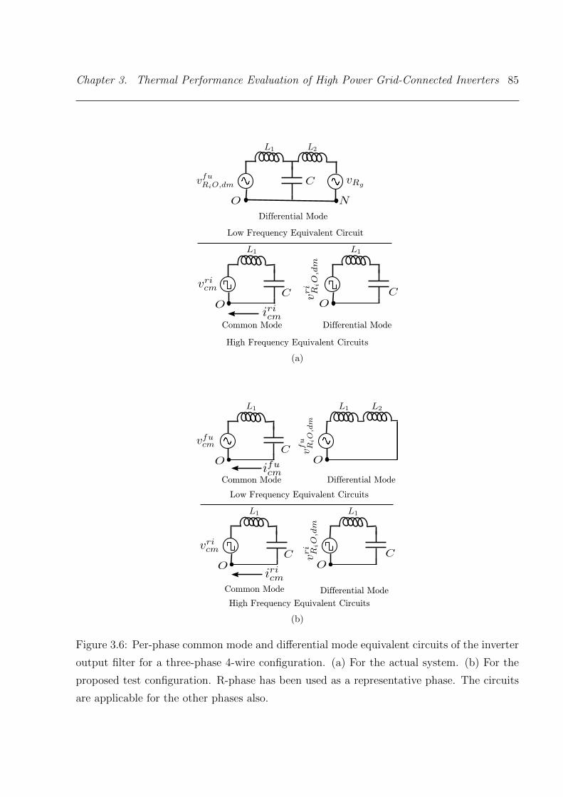
Chapter 3. Thermal Performance Evaluation of High Power Grid-Connected Inverters 85
Common Mode Differential Mode
Differential Mode
Low Frequency Equivalent Circuit
High Frequency Equivalent Circuits
(a)
Common Mode Differential Mode
Low Frequency Equivalent Circuits
High Frequency Equivalent Circuits
Common Mode Differential Mode
(b)
Figure 3.6: Per-phase common mode and differential mode equivalent circuits of the inverter
output filter for a three-phase 4-wire configuration. (a) For the actual system. (b) For the
proposed test configuration. R-phase has been used as a representative phase. The circuits
are applicable for the other phases also.
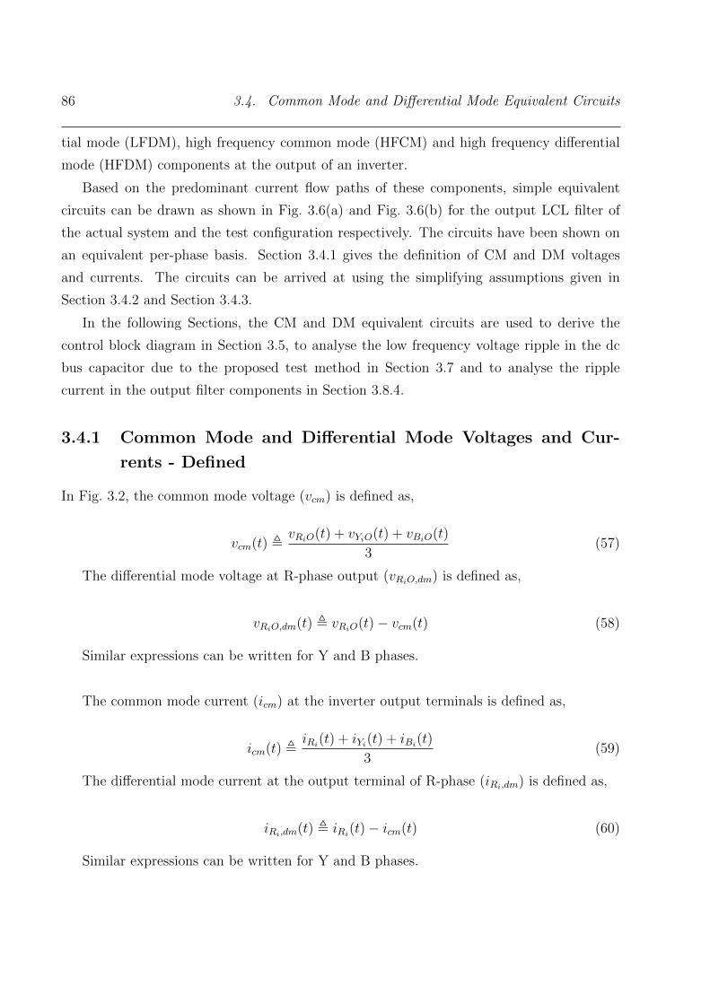
86 3.4. Common Mode and Differential Mode Equivalent Circuits
tial mode (LFDM), high frequency common mode (HFCM) and high frequency differential
mode (HFDM) components at the output of an inverter.
Based on the predominant current flow paths of these components, simple equivalent
circuits can be drawn as shown in Fig. 3.6(a) and Fig. 3.6(b) for the output LCL filter of
the actual system and the test configuration respectively. The circuits have been shown on
an equivalent per-phase basis. Section 3.4.1 gives the definition of CM and DM voltages
and currents. The circuits can be arrived at using the simplifying assumptions given in
Section 3.4.2 and Section 3.4.3.
In the following Sections, the CM and DM equivalent circuits are used to derive the
control block diagram in Section 3.5, to analyse the low frequency voltage ripple in the dc
bus capacitor due to the proposed test method in Section 3.7 and to analyse the ripple
current in the output filter components in Section 3.8.4.
3.4.1 Common Mode and Differential Mode Voltages and Cur-
rents - Defined
In Fig. 3.2, the common mode voltage (vcm) is defined as,
vcm(t) ,vRiO(t) + vYiO(t) + vBiO(t)
3(57)
The differential mode voltage at R-phase output (vRiO,dm) is defined as,
vRiO,dm(t) , vRiO(t)− vcm(t) (58)
Similar expressions can be written for Y and B phases.
The common mode current (icm) at the inverter output terminals is defined as,
icm(t) ,iRi
(t) + iYi(t) + iBi(t)
3(59)
The differential mode current at the output terminal of R-phase (iRi,dm) is defined as,
iRi,dm(t) , iRi(t)− icm(t) (60)
Similar expressions can be written for Y and B phases.
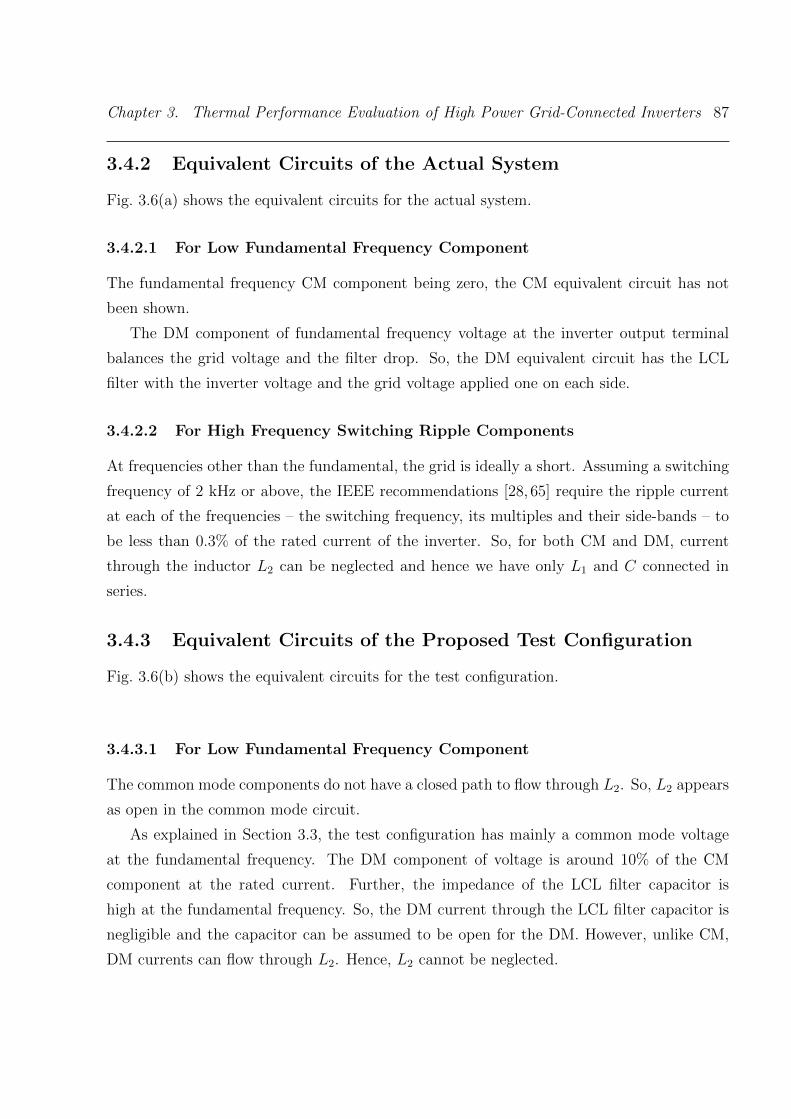
Chapter 3. Thermal Performance Evaluation of High Power Grid-Connected Inverters 87
3.4.2 Equivalent Circuits of the Actual System
Fig. 3.6(a) shows the equivalent circuits for the actual system.
3.4.2.1 For Low Fundamental Frequency Component
The fundamental frequency CM component being zero, the CM equivalent circuit has not
been shown.
The DM component of fundamental frequency voltage at the inverter output terminal
balances the grid voltage and the filter drop. So, the DM equivalent circuit has the LCL
filter with the inverter voltage and the grid voltage applied one on each side.
3.4.2.2 For High Frequency Switching Ripple Components
At frequencies other than the fundamental, the grid is ideally a short. Assuming a switching
frequency of 2 kHz or above, the IEEE recommendations [28, 65] require the ripple current
at each of the frequencies – the switching frequency, its multiples and their side-bands – to
be less than 0.3% of the rated current of the inverter. So, for both CM and DM, current
through the inductor L2 can be neglected and hence we have only L1 and C connected in
series.
3.4.3 Equivalent Circuits of the Proposed Test Configuration
Fig. 3.6(b) shows the equivalent circuits for the test configuration.
3.4.3.1 For Low Fundamental Frequency Component
The common mode components do not have a closed path to flow through L2. So, L2 appears
as open in the common mode circuit.
As explained in Section 3.3, the test configuration has mainly a common mode voltage
at the fundamental frequency. The DM component of voltage is around 10% of the CM
component at the rated current. Further, the impedance of the LCL filter capacitor is
high at the fundamental frequency. So, the DM current through the LCL filter capacitor is
negligible and the capacitor can be assumed to be open for the DM. However, unlike CM,
DM currents can flow through L2. Hence, L2 cannot be neglected.
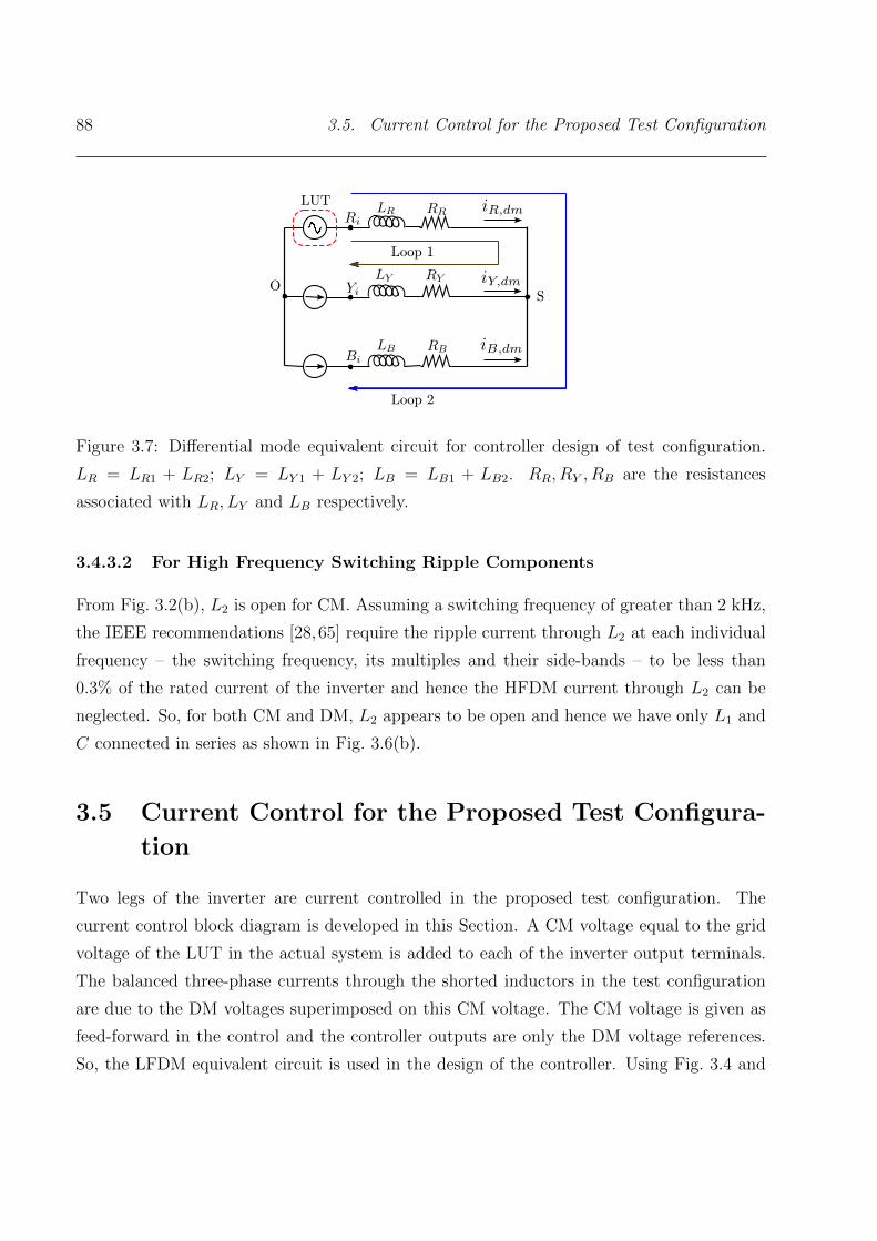
88 3.5. Current Control for the Proposed Test Configuration
LUT
SO
Loop 1
Loop 2
Figure 3.7: Differential mode equivalent circuit for controller design of test configuration.
LR = LR1 + LR2; LY = LY 1 + LY 2; LB = LB1 + LB2. RR, RY , RB are the resistances
associated with LR, LY and LB respectively.
3.4.3.2 For High Frequency Switching Ripple Components
From Fig. 3.2(b), L2 is open for CM. Assuming a switching frequency of greater than 2 kHz,
the IEEE recommendations [28,65] require the ripple current through L2 at each individual
frequency – the switching frequency, its multiples and their side-bands – to be less than
0.3% of the rated current of the inverter and hence the HFDM current through L2 can be
neglected. So, for both CM and DM, L2 appears to be open and hence we have only L1 and
C connected in series as shown in Fig. 3.6(b).
3.5 Current Control for the Proposed Test Configura-
tion
Two legs of the inverter are current controlled in the proposed test configuration. The
current control block diagram is developed in this Section. A CM voltage equal to the grid
voltage of the LUT in the actual system is added to each of the inverter output terminals.
The balanced three-phase currents through the shorted inductors in the test configuration
are due to the DM voltages superimposed on this CM voltage. The CM voltage is given as
feed-forward in the control and the controller outputs are only the DM voltage references.
So, the LFDM equivalent circuit is used in the design of the controller. Using Fig. 3.4 and
Chapter 3. Thermal Performance Evaluation of High Power Grid-Connected Inverters 89
Fig. 3.6(b) the DM equivalent circuit for current control is shown in Fig. 3.7.
By Kirchhoff’s Current Law (KCL), iR,dm = −(iY,dm+iB,dm). So, by applying Kirchhoff’s
voltage law (KVL) around loop 1 and loop 2 shown in Fig. 3.7 and using the subscripts ‘cm’
and ‘dm’ to represent the common mode and differential mode components respectively of
currents and voltages, we have the following system of equations:
[vYiO,dm
vBiO,dm
]=
[(RR +RY ) RR
RR (RR +RB)
][iY,dm
iB,dm
]
+
[(LR + LY ) LR
LR (LR + LB)
][diY,dm/dt
diB,dm/dt
]
+
[vRiO,dm
vRiO,dm
](61)
where, RR, RY and RB are the resistances associated with the inductors and LR =
LR1 + LR2, LY = LY 1 + LY 2, LB = LB1 + LB2.
The above equations represent a multiple input (iY,dm, iB,dm, vRiO,dm) multiple output
(vYiO,dm, vBiO,dm) system. The following substitution is used to convert the system into two
independent decoupled systems.
[v′Y
v′B
]=
[vYiO,dm
vBiO,dm
]−
[RR RR
RR RR
][iY,dm
iB,dm
]
−
[LR LR
LR LR
][diY,dm/dt
diB,dm/dt
]
−
[vRiO,dm
vRiO,dm
](62)
Using (61), (62) and assuming an equal inductance (L) and associated resistance (R) in
each of the phases, we have,[v′Y
v′B
]=
[R 0
0 R
][iY,dm
iB,dm
]+
[L 0
0 L
][diY,dm/dt
diB,dm/dt
](63)
The requirement is to regulate the currents iY,dm and iB,dm. The control is similar to the
current control of a RL circuit. Fig. 3.8 shows the control block diagram. The block diagram

90 3.6. Base Values, System Parameters and Control Parameters
has been shown for Y leg. The same is applicable to B leg also. A proportional resonant
(PR) controller has been used. In Fig. 3.8, i∗Y,dm represents the set reference current. Kp and
Kr are the PR controller constants. ωr = 2 ·π ·50 rad/s. References [98–100] discuss in detail
the selection of controller constants for the PR controller and the digital implementation of
the same.
From (62) and (63), assuming an equal inductance (L) and associated resistance (R) in
all the phases, the differential mode component of the voltage references vYiO,dm and vBiO,dm
for the current controlled legs are given by,
vYiO,dm = 2 · v′Y + v′B + vRiO,dm (64)
vBiO,dm = 2 · v′B + v′Y + vRiO,dm (65)
The actual voltage references for the current controlled legs including the common mode
voltage component are given by,
vYiO = vYiO,dm + vcm (66)
vBiO = vBiO,dm + vcm (67)
Considering the R-phase leg as the LUT, vcm = vRg . The complete control block diagram
is shown in Fig. 3.9.
3.6 Base Values, System Parameters and Control Pa-
rameters
Analysis and experimental validation of the proposed method was carried out on an inverter
at a rating of 24 kVA. A single-phase front-end converter was used to charge the dc bus.
Both the front-end converter and the inverter were controlled using a single TMS320F2812
DSP board. Sine-triangle modulation was used for the case of three-phase 4-wire system
and conventional space vector PWM (CSVPWM) was used for the case of three-phase 3-
wire system. The dc bus voltage was set to 800 V in case of sine-triangle PWM and was
lowered to 700 V in case of CSVPWM to have similar modulation indices in both the cases.
Passive damping was used to suppress resonance in the output LCL filter. The base values

Chapter 3. Thermal Performance Evaluation of High Power Grid-Connected Inverters 91
PR Controller
Figure 3.8: Block diagram for current control shown for Y phase. The current control is
implemented for two phases of the inverter.
2
2
PR
PR
Figure 3.9: Complete control block diagram for the test configuration. R-phase is assumed
to be the LUT. vRiO is an open loop voltage. vRiO is set to be the same as the voltage at
the R-phase output terminal of the inverter in the actual system.
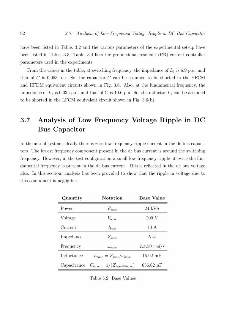
92 3.7. Analysis of Low Frequency Voltage Ripple in DC Bus Capacitor
have been listed in Table. 3.2 and the various parameters of the experimental set-up have
been listed in Table. 3.3. Table. 3.4 lists the proportional-resonant (PR) current controller
parameters used in the experiments.
From the values in the table, at switching frequency, the impedance of L1 is 6.9 p.u. and
that of C is 0.053 p.u. So, the capacitor C can be assumed to be shorted in the HFCM
and HFDM equivalent circuits shown in Fig. 3.6. Also, at the fundamental frequency, the
impedance of L1 is 0.035 p.u. and that of C is 10.6 p.u. So, the inductor L1 can be assumed
to be shorted in the LFCM equivalent circuit shown in Fig. 3.6(b).
3.7 Analysis of Low Frequency Voltage Ripple in DC
Bus Capacitor
In the actual system, ideally there is zero low frequency ripple current in the dc bus capaci-
tors. The lowest frequency component present in the dc bus current is around the switching
frequency. However, in the test configuration a small low frequency ripple at twice the fun-
damental frequency is present in the dc bus current. This is reflected in the dc bus voltage
also. In this section, analysis has been provided to show that the ripple in voltage due to
this component is negligible.
Quantity Notation Base Value
Power Pbase 24 kVA
Voltage Vbase 200 V
Current Ibase 40 A
Impedance Zbase 5 Ω
Frequency ωbase 2.π.50 rad/s
Inductance Lbase = Zbase/ωbase 15.92 mH
Capacitance Cbase = 1/(Zbase.ωbase) 636.62 µF
Table 3.2: Base Values

Chapter 3. Thermal Performance Evaluation of High Power Grid-Connected Inverters 93
Quantity Notation Value Per Unit
Inverter 3-phase power Prated 24 kVA 1.0
Fundamental frequency ffu 50 Hz 1.0
Switching frequency fsw 10 kHz 200
DC bus voltage (Sine-triangle) Vdc 800 V 4.0
DC bus voltage (CSVPWM) Vdc 700 V 3.5
Grid phase voltage Vg 200 V 1.0
Rated line current Irated 40 A 1.0
DC bus capacitance CDC 9400 µF 14.77
Inverter-side inductor L1 550 µH 0.035
Grid-side inductor L2 550 µH 0.035
Filter capacitance C1 30 µF 0.047
Damping branch capacitance Cd 30 µF 0.047
Total filter capacitance C = C1 + Cd 60 µF 0.094
Damping inductance Ld 390 µH 0.025
Damping resistance Rd 3 Ω 0.6
Table 3.3: System Parameters

94 3.7. Analysis of Low Frequency Voltage Ripple in DC Bus Capacitor
Control Parameter Value
Kp 1.42 Ω
Kr 138.39 V/A− s
Table 3.4: Current Controller Parameters
3.7.1 Low Frequency Ripple due to Output Fundamental CM Com-
ponent
Using the LFCM equivalent circuit shown in Fig. 3.6(b) and shorting the inductor L1 as
suggested in the previous Section, the LFCM circuit reduces to a voltage applied to a simple
capacitor. The grid voltage is the CM voltage in the test configuration as shown in Fig. 3.5(b).
Considering R-phase to be the LUT, let the grid voltage and hence the CM voltage vcm(t)
at the output of the test configuration be given by,
vcm(t) = vRg(t) = Vmsin(ωt) (68)
where, Vm = Vg√
2 and ω = 2 ·π · ffu. At steady state, the current icm(t) due to this CM
voltage is,
icm(t) = Vm · ωC · sin(ωt+ 90o) (69)
So, the total instantaneous ac side power due to the CM voltage and current in the three
phases is,
pcm(t) = −3
2· V 2
m · ωC · cos(2ωt+ 90o) (70)
By equating the above to the input side power, the input side low frequency current
ripple and the corresponding input side low frequency voltage ripple can be computed. The
peak-to-peak low frequency voltage ripple Vripple,pk−pk in the dc bus can be derived to be,
Vripple,pk−pk =3 · V 2
g · CVdc · CDC
(71)
Using values in Table. 3.3, Vripple,pk−pk = 0.957V or 0.0048p.u. which is negligible.
Chapter 3. Thermal Performance Evaluation of High Power Grid-Connected Inverters 95
3.7.2 Low Frequency Ripple due to Output Fundamental DM
Component
Let the fundamental frequency component of currents at the output be given by,
iR(t) = Imsin(ωt− φ) (72)
iY (t) = Imsin(ωt− φ− 120o) (73)
iB(t) = Imsin(ωt− φ+ 120o) (74)
where, Im = Irated√
2, ω = 2 · π · ffu and φ is the phase angle measured with respect to
the R-phase grid voltage.
Using the LFCM equivalent circuit shown in Fig. 3.6(b), at steady state, the fundamental
frequency voltages across the output filter inductors are given by,
vLR(t) = ω(LR1 + LR2) · Imsin(ωt− φ+ 90o) (75)
vLY(t) = ω(LY 1 + LY 2) · Imsin(ωt− φ− 120o + 90o) (76)
vLB(t) = ω(LB1 + LB2) · Imsin(ωt− φ+ 120o + 90o) (77)
So, the total instantaneous ac side power due to the DM voltage and current in the three
phases is,
pdm(t) = vLR(t) · iR(t) + vLY
(t) · iY (t) + vLB(t) · iB(t) (78)
(78) on simplification shows the total instantaneous power due to the DM components
of voltage and current at the inverter output to be zero. Hence, the low frequency dc bus
voltage ripple due to DM component is zero. This indicates that ideally power circulates
among the three phases and only the losses are drawn from the dc side in case of the DM
component.
96 3.8. Analysis and Experimental Results – 4-Wire Configuration
From Section 3.7.1 and Section 3.7.2, it can be concluded that only the CM component
of currents at the output lead to low frequency ripple in the dc bus and the magnitude of
the ripple is negligible.
3.8 Analysis and Experimental Results – 4-Wire Con-
figuration
3.8.1 Current Control
Fig. 3.10 shows the three phase currents iR, iY , iB and the voltage vC across the R-phase
LCL filter capacitor while emulating a grid-connected inverter that injects a 90o lagging
current, an in-phase current, a 90o leading current and an 180o out-of-phase current at the
point of common coupling with the grid using the control method discussed in Section 3.5.
The experimental parameters are as shown in Table. 3.3.
3.8.2 Thermal Testing of Semiconductor Devices
The thermal testing of semiconductor devices aims at subjecting the individual semiconduc-
tor devices to similar junction thermal stress as the actual system operating at the rated
conditions. Usually the device junction is not accessible for temperature measurement. So,
the junction temperature is estimated from the heatsink temperature using simple steady-
state thermal models [101]. In some IGBT modules, the case temperature can be measured
using in-built temperature sensors [101]. In such cases, the case temperature can be used
for more accurate estimation of the junction temperature. In this thesis, the heatsink tem-
perature is used. Fig. 3.11 shows the thermal model of the system under test (SUT) shown
in Fig. 3.2. From Fig. 3.11, it can be observed that, to have the same junction temperature
as the actual system in the test configuration, it is required that,
• The heatsink temperature in the test configuration is the same as that of the actual
system operating at the rated conditions.
• The power loss in the individual semiconductor device being tested is the same as the
actual system operating at the rated conditions.
Further, it must be ensured that the power loss in the semiconductor devices other than
the device being tested do not exceed the maximum loss for that device in the actual system.

Chapter 3. Thermal Performance Evaluation of High Power Grid-Connected Inverters 97
Section 3.8.2.1 and Section 3.8.2.2 analyses the heatsink temperature and the power loss in
individual semiconductor devices in the actual system and the test configuration.
3.8.2.1 Heatsink Temperature
The heatsink temperature can be analytically estimated from the total losses generated
by the semiconductor devices mounted on the heatsink using the thermal resistance of the
heatsink. In the experimental set-up, three SKM150GB12T4G [102] IGBT modules - one
for each leg of the three-phase inverter - are used. All the modules are mounted on a
(a) (b)
(c) (d)
Figure 3.10: Three phase currents CH1: iR, CH2: iY , CH3: iB and R-phase LCL filter
capacitor voltage CH4: vC in the test configuration while emulating a grid-connected inverter
that injects (a) a 90o lagging current (b) an in-phase current (c) a 90o leading current (d)
an 180o out-of-phase current at the point of common coupling with the grid. Experimental
parameters are as shown in Table. 3.3. CH1, CH2, CH3: 50A/div; CH4: 100V/div.

98 3.8. Analysis and Experimental Results – 4-Wire Configuration
h
h
Figure 3.11: Thermal model of the three-phase inverter shown in Fig. 3.2. The detailed
model of one leg is shown. The blocks ‘Y Phase Leg’ and ‘B Phase Leg’ also have the same
thermal model as the R-phase leg. Rth,h−a, Rth,c−h, Rth,j−c,IGBT , Rth,j−c,Diode are the thermal
resistances of heatsink, case to heatsink including heatsink paste, IGBT junction to case and
Diode junction to case respectively. PS1, PD1, PS2 and PD2 are the average power loss in the
devices S1, D1, S2 and D2 shown in Fig. 3.2.

Chapter 3. Thermal Performance Evaluation of High Power Grid-Connected Inverters 99
common heatsink. The total loss in each switching element SW1 through SW6 shown in
Fig. 3.2(b) consists of the IGBT conduction loss (PS cond), diode conduction loss (PD cond),
IGBT switching loss (PS sw) and the diode reverse recovery loss (PD rr). At higher currents,
the terminal losses of the modules (PMod term) are also included. The analytical computation
of the various power loss components in the IGBT and anti-parallel diode has been done
using the datasheet parameters based on [101, 103, 104]. The effect of output current ripple
on the heatsink temperature rise over ambient is negligible as discussed in [101, 103] and
hence has been neglected in the power loss computations. Appendix E gives the equations
related to the power loss computations.
The datasheet parameters required to compute the power loss components are dependent
on the gate drive resistance, operating current and the maximum operating junction tem-
perature. The various values of the datasheet parameters used for analytical computation
of the heatsink temperature are listed in Table 3.5.
Power Loss in One Leg of Inverter: Fig. 3.12(a) shows the plot of the analytically
computed loss components in one leg of the inverter for varying load angle or power factor
angle, φ. φ is the angle between fundamental frequency voltage and current at the grid-end
of the inverter output filter. In Fig. 3.2(a), φ is computed from the voltage and current
measured at one of the nodes Rg, Yg or Bg and in Fig. 3.2(b), the measurement node is ‘S’.
The current direction for φ is assumed to be outward from the inverter as indicated by one
of the currents iR, iY or iB in Fig. 3.2(a) and Fig. 3.2(b). The voltages measurement at
the grid-end is considered with respect to the dc bus mid-point ‘O’. As seen in the plot, the
IGBT switching loss and the diode reverse recovery loss are constant for a chosen switching
frequency. But, the conduction losses in the IGBT and diode vary sinusoidally with load
angle as the average conduction period of the IGBT and diode varies with the load angle.
The sinusoidal variation in the total loss with varying φ can be observed from the magnified
view of the total power loss curve shown in Fig. 3.12(b) as well as from the expressions given
in Appendix E.
This sinusoidal variation in the total power loss in one leg of the inverter can be repre-
sented as,
P (φ) = Po + Pmsin(φ− 90o) (79)
P (φ) represents the total power loss at a given φ. Po represents the average total power
loss and Pm represents the peak of the sinusoidal component of total power loss for varying
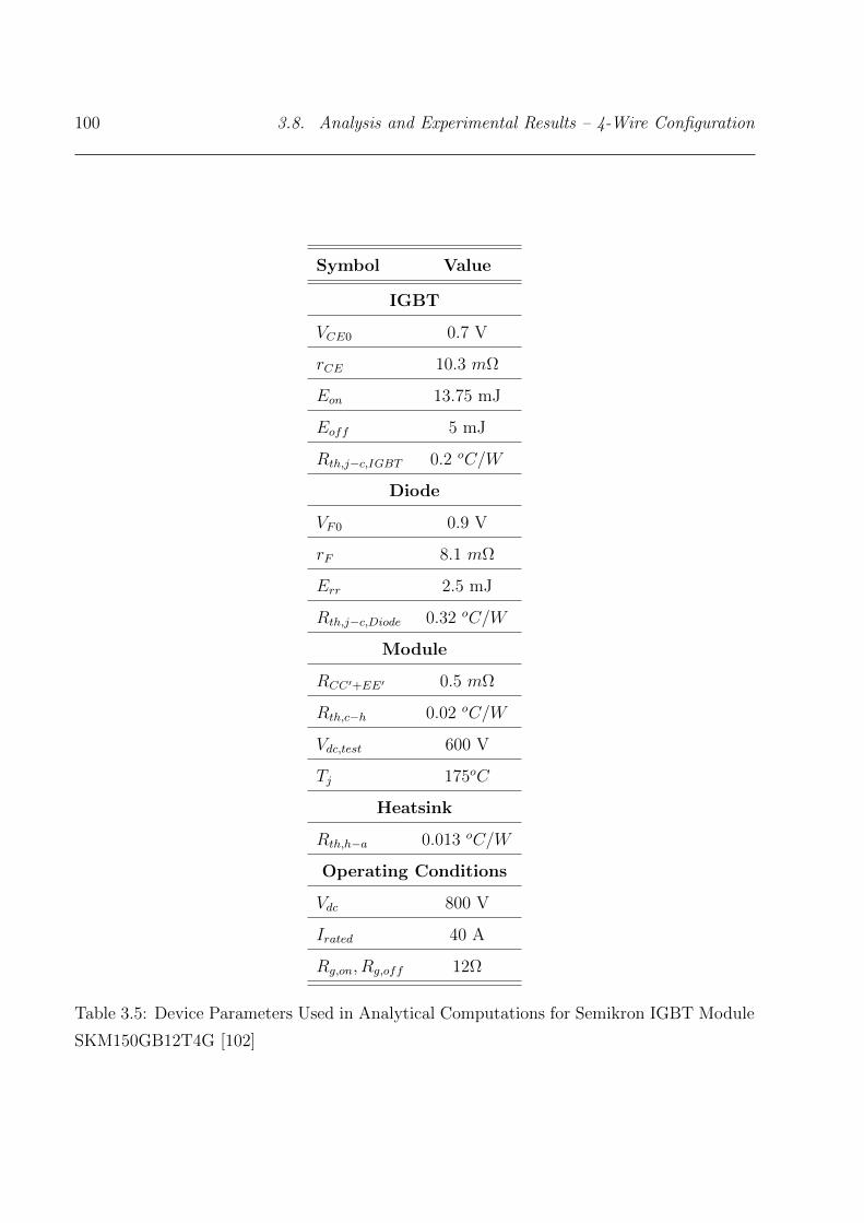
100 3.8. Analysis and Experimental Results – 4-Wire Configuration
Symbol Value
IGBT
VCE0 0.7 V
rCE 10.3 mΩ
Eon 13.75 mJ
Eoff 5 mJ
Rth,j−c,IGBT 0.2 oC/W
Diode
VF0 0.9 V
rF 8.1 mΩ
Err 2.5 mJ
Rth,j−c,Diode 0.32 oC/W
Module
RCC′+EE′ 0.5 mΩ
Rth,c−h 0.02 oC/W
Vdc,test 600 V
Tj 175oC
Heatsink
Rth,h−a 0.013 oC/W
Operating Conditions
Vdc 800 V
Irated 40 A
Rg,on, Rg,off 12Ω
Table 3.5: Device Parameters Used in Analytical Computations for Semikron IGBT Module
SKM150GB12T4G [102]
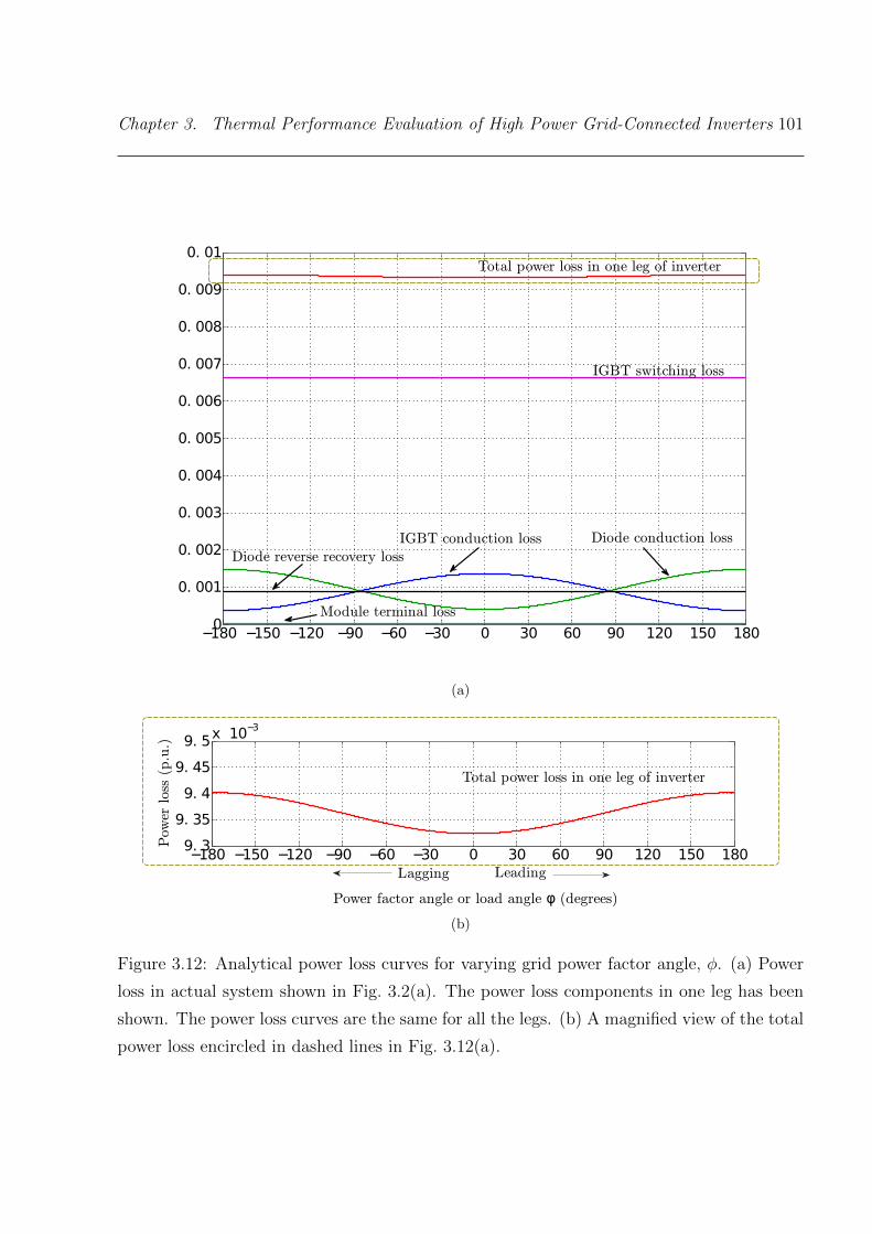
Chapter 3. Thermal Performance Evaluation of High Power Grid-Connected Inverters 101
−180 −150 −120 −90 −60 −30 0 30 60 90 120 150 1800
0. 001
0. 002
0. 003
0. 004
0. 005
0. 006
0. 007
0. 008
0. 009
0. 01Total power loss in one leg of inverter
IGBT switching loss
Diode conduction lossIGBT conduction loss
Diode reverse recovery loss
Module terminal loss
(a)
−180 −150 −120 −90 −60 −30 0 30 60 90 120 150 1809. 3
9. 35
9. 4
9. 45
9. 5x 10⁻³
Power factor angle or load angle φ (degrees)
Powerloss(p.u.)
Leading
Total power loss in one leg of inverter
Lagging
(b)
Figure 3.12: Analytical power loss curves for varying grid power factor angle, φ. (a) Power
loss in actual system shown in Fig. 3.2(a). The power loss components in one leg has been
shown. The power loss curves are the same for all the legs. (b) A magnified view of the total
power loss encircled in dashed lines in Fig. 3.12(a).

102 3.8. Analysis and Experimental Results – 4-Wire Configuration
φ.
Total Power Loss in Actual System and Test Configuration: The power factor
angle φ is the same for the three legs in the actual system as the three-phase grid voltages
and the three-phase grid currents are balanced. This can also be observed in Fig. 3.5(a) from
phasors VRg , VYg , VBg , IR, IY and IB. Thus, the power loss in the inverter for the actual
system is 3 · P (φ).
In the test configuration, the voltage at the short circuit point corresponds to the grid
voltage of the LUT and the three-phase currents are balanced. So, the power factor angle
is φ for the LUT and are (φ− 120o) and (φ+ 120o) for the other two legs. This can also be
observed in Fig. 3.5(b) from phasors VS, IR, IY and IB. Thus, the power loss in the inverter
for the test configuration is P (φ)+P (φ−120o)+P (φ+120o) = 3 ·Po. The power loss curves
for the individual phase legs in the test configuration has been shown in Fig. 3.13.
−180 −150 −120 −90 −60 −30 0 30 60 90 120 150 1809.32
9.33
9.34
9.35
9.36
9.37
9.38
9.39
9.4
9.41x 10⁻³
Power factor angle or load angle φ (degree)
Totalpowerloss(p.u.)
Y phase leg R phase leg
LeadingLagging
B phase leg
Figure 3.13: Analytical power loss curves in test configuration shown in Fig. 3.2(b) for the
phases R,Y and B. The power loss has been shown for varying grid power factor angle, φ.
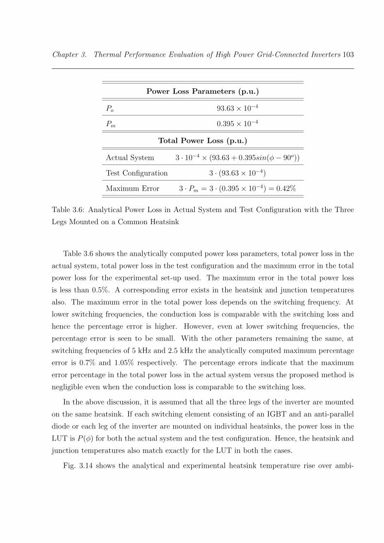
Chapter 3. Thermal Performance Evaluation of High Power Grid-Connected Inverters 103
Power Loss Parameters (p.u.)
Po 93.63× 10⁻⁴
Pm 0.395× 10⁻⁴
Total Power Loss (p.u.)
Actual System 3 · 10−4 × (93.63 + 0.395sin(φ− 90o))
Test Configuration 3 · (93.63× 10−4)
Maximum Error 3 · Pm = 3 · (0.395× 10−4) = 0.42%
Table 3.6: Analytical Power Loss in Actual System and Test Configuration with the Three
Legs Mounted on a Common Heatsink
Table 3.6 shows the analytically computed power loss parameters, total power loss in the
actual system, total power loss in the test configuration and the maximum error in the total
power loss for the experimental set-up used. The maximum error in the total power loss
is less than 0.5%. A corresponding error exists in the heatsink and junction temperatures
also. The maximum error in the total power loss depends on the switching frequency. At
lower switching frequencies, the conduction loss is comparable with the switching loss and
hence the percentage error is higher. However, even at lower switching frequencies, the
percentage error is seen to be small. With the other parameters remaining the same, at
switching frequencies of 5 kHz and 2.5 kHz the analytically computed maximum percentage
error is 0.7% and 1.05% respectively. The percentage errors indicate that the maximum
error percentage in the total power loss in the actual system versus the proposed method is
negligible even when the conduction loss is comparable to the switching loss.
In the above discussion, it is assumed that all the three legs of the inverter are mounted
on the same heatsink. If each switching element consisting of an IGBT and an anti-parallel
diode or each leg of the inverter are mounted on individual heatsinks, the power loss in the
LUT is P (φ) for both the actual system and the test configuration. Hence, the heatsink and
junction temperatures also match exactly for the LUT in both the cases.
Fig. 3.14 shows the analytical and experimental heatsink temperature rise over ambi-
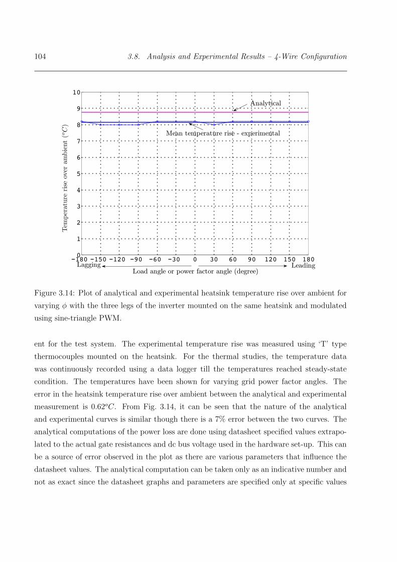
104 3.8. Analysis and Experimental Results – 4-Wire Configuration
−180 −150 −120 −90 −60 −30 0 30 60 90 120 150 1800
1
2
3
4
5
6
7
8
9
10
Load angle or power factor angle (degree)
Analytical
Mean temperature rise - experimental
LeadingLagging
Figure 3.14: Plot of analytical and experimental heatsink temperature rise over ambient for
varying φ with the three legs of the inverter mounted on the same heatsink and modulated
using sine-triangle PWM.
ent for the test system. The experimental temperature rise was measured using ‘T’ type
thermocouples mounted on the heatsink. For the thermal studies, the temperature data
was continuously recorded using a data logger till the temperatures reached steady-state
condition. The temperatures have been shown for varying grid power factor angles. The
error in the heatsink temperature rise over ambient between the analytical and experimental
measurement is 0.62oC. From Fig. 3.14, it can be seen that the nature of the analytical
and experimental curves is similar though there is a 7% error between the two curves. The
analytical computations of the power loss are done using datasheet specified values extrapo-
lated to the actual gate resistances and dc bus voltage used in the hardware set-up. This can
be a source of error observed in the plot as there are various parameters that influence the
datasheet values. The analytical computation can be taken only as an indicative number and
not as exact since the datasheet graphs and parameters are specified only at specific values
Chapter 3. Thermal Performance Evaluation of High Power Grid-Connected Inverters 105
of junction temperatures of the IGBT and diode. The worst case junction temperature is
considered for the analytical estimates.
3.8.2.2 Power Loss in Individual Semiconductor Devices
Besides the datasheet parameters of the semiconductor devices, the power loss in the indi-
vidual semiconductor devices are dependent on the modulation index m, Im = Irated ·√
2,
angle ψ between the voltage and current at the inverter output terminal, switching frequency
fsw and the dc bus voltage Vdc. The output voltage and current are maintained the same for
the LUT in both the actual system and the test configuration. So, all the above mentioned
parameters and hence the power loss in the individual semiconductor devices are the same
for the LUT in both the cases.
Further, as mentioned in the previous subsection, the other two legs resemble the LUT
except for the power factor angles which are (φ − 120o) and (φ + 120o) respectively. So,
for the test configuration, it is ensured that the power loss in the individual semiconductor
devices of these legs do not exceed the maximum values expected in the actual system if the
inverter is expected to operate in the full range of power factors. The same can be observed
from Fig. 3.13. The peak power loss is the same for the three individual legs.
Thus, the semiconductor device thermal testing can be performed satisfactorily using the
test configuration for either case of a common or an individual heatsink for the switching
elements or modules.
3.8.2.3 Input Power
The input power requirement is less since only the losses in the test configuration needs to be
supplied from the input. The input power drawn varied between 1038W to 1108W for load
angle variations from −180o to +180o with the output power being 24kV A. The input power
is ' 4.5% of the output VA and corresponds to the losses in the test configuration including
the front-end converter. The losses in the front-end converter is less as the current drawn
from the input is less. Thus, there is a near 50% reduction in the total power consumed by
the proposed thermal test as compared to using two inverters of same rating to perform the
thermal test as suggested in existing literature [96].

106 3.8. Analysis and Experimental Results – 4-Wire Configuration
3.8.3 Testing of DC Bus Capacitors
The temperature rise and hence the life of the dc bus electrolytic capacitors is dependent on
the rms current flowing through the capacitor [16]. The equivalent series resistance (ESR)
that causes the temperature rise is frequency-dependent [105, 106]. Hence, the frequency
spectrum of the current is also equally important along with the rms value. The rms current
and the current spectrum of the dc bus capacitor current in the test configuration will be the
same as that of the actual system if icap(t), the instantaneous dc bus capacitor current, is the
same in both the cases. icap(t) is indicated in Fig. 3.2(b). Equivalently, the ac component of
the instantaneous dc link current ilink(t) shown in Fig. 3.2(b) can also be considered.
From Fig. 3.2(b), the instantaneous dc link current (ilink(t)) in a two-level inverter is
given by [16],
ilink(t) = SR(t) · iRi(t) + SY (t) · iYi(t) + SB(t) · iBi
(t) (80)
where, SR(t), SY (t) and SB(t) are the instantaneous switch states of the top IGBTs S1,
S3 and S5 respectively of the three phase legs R, Y and B of the inverter shown in Fig. 3.2(b).
The switch state of an IGBT is ‘1’ when it is ON and is ‘0’ when it is OFF. iRi(t), iYi(t) and
iBi(t) are the instantaneous fundamental frequency currents in the inverter-side inductors of
the inverter as shown in Fig. 3.2. The effect of the inverter output ripple current on the dc
bus capacitor current is negligible [16] and has been ignored. The fundamental frequency
current through the output filter capacitors is negligible. Hence, currents iRi, iYi and iBi
can
be replaced by iR, iY and iB respectively. Then, we have,
ilink(t) = SR(t) · iR(t) + SY (t) · iY (t) + SB(t) · iB(t) (81)
From (81), if the test method ensures that the instantaneous switch states and the in-
stantaneous output grid-side inductor currents are the same as the actual system, then the
ac component of ilink(t) and hence icap(t) will be identical for the test configuration and the
actual system. The dc component of ilink(t) is dependent on the losses in the switching de-
vices and on the losses at the output. However, since the dc component of ilink(t) is supplied
by the front-end converter or any dc source that is connected to the dc bus capacitors to
supply the losses in the system, it is not of interest in the thermal testing of dc bus capacitors.
Fig. 3.15(a) and Fig. 3.15(b) show the three-phase inverter output voltages and output
grid-side inductor currents for the actual system and the test configuration for a represen-
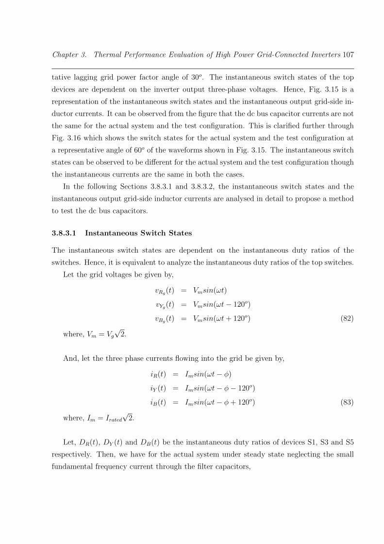
Chapter 3. Thermal Performance Evaluation of High Power Grid-Connected Inverters 107
tative lagging grid power factor angle of 30o. The instantaneous switch states of the top
devices are dependent on the inverter output three-phase voltages. Hence, Fig. 3.15 is a
representation of the instantaneous switch states and the instantaneous output grid-side in-
ductor currents. It can be observed from the figure that the dc bus capacitor currents are not
the same for the actual system and the test configuration. This is clarified further through
Fig. 3.16 which shows the switch states for the actual system and the test configuration at
a representative angle of 60o of the waveforms shown in Fig. 3.15. The instantaneous switch
states can be observed to be different for the actual system and the test configuration though
the instantaneous currents are the same in both the cases.
In the following Sections 3.8.3.1 and 3.8.3.2, the instantaneous switch states and the
instantaneous output grid-side inductor currents are analysed in detail to propose a method
to test the dc bus capacitors.
3.8.3.1 Instantaneous Switch States
The instantaneous switch states are dependent on the instantaneous duty ratios of the
switches. Hence, it is equivalent to analyze the instantaneous duty ratios of the top switches.
Let the grid voltages be given by,
vRg(t) = Vmsin(ωt)
vYg(t) = Vmsin(ωt− 120o)
vBg(t) = Vmsin(ωt+ 120o) (82)
where, Vm = Vg√
2.
And, let the three phase currents flowing into the grid be given by,
iR(t) = Imsin(ωt− φ)
iY (t) = Imsin(ωt− φ− 120o)
iB(t) = Imsin(ωt− φ+ 120o) (83)
where, Im = Irated√
2.
Let, DR(t), DY (t) and DB(t) be the instantaneous duty ratios of devices S1, S3 and S5
respectively. Then, we have for the actual system under steady state neglecting the small
fundamental frequency current through the filter capacitors,

108 3.8. Analysis and Experimental Results – 4-Wire Configuration
0 30 60 90 120 150 180 210 240 270 300 330 360−400
−300
−200
−100
0
100
200
300
400
Phase angle in degrees
MagnitudeinVorA
vB ivYi
iY iB
60o line
vR i
iR
(a)
0 30 60 90 120 150 180 210 240 270 300 330 360−400
−300
−200
−100
0
100
200
300
400
Phase angle in degrees
MagnitudeinVorA
vYivB i
iY iB
60o line
vR i
iR
(b)
Figure 3.15: Three-phase inverter voltages (vRi, vYi and vBi
) and three-phase grid-side in-
ductor currents (iR, iY and iB) for a lagging grid power factor angle of 30o. (a) In the actual
system. (b) In the test configuration.
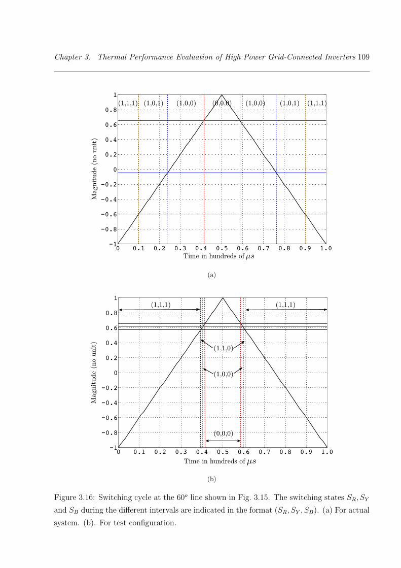
Chapter 3. Thermal Performance Evaluation of High Power Grid-Connected Inverters 109
0 0.1 0.2 0.3 0.4 0.5 0.6 0.7 0.8 0.9 1.0−1
−0.8
−0.6
−0.4
−0.2
0
0.2
0.4
0.6
0.8
1Magnitude(nounit)
(1,1,1) (1,0,1) (1,0,0) (0,0,0) (1,0,0) (1,0,1) (1,1,1)
Time in hundreds of
(a)
0 0.1 0.2 0.3 0.4 0.5 0.6 0.7 0.8 0.9 1.0−1
−0.8
−0.6
−0.4
−0.2
0
0.2
0.4
0.6
0.8
1
Magnitude(nounit)
Time in hundreds of
(1,1,1) (1,1,1)
(1,0,0)
(1,1,0)
(0,0,0)
(b)
Figure 3.16: Switching cycle at the 60o line shown in Fig. 3.15. The switching states SR, SY
and SB during the different intervals are indicated in the format (SR, SY , SB). (a) For actual
system. (b). For test configuration.

110 3.8. Analysis and Experimental Results – 4-Wire Configuration
DR(t)act =1
2+
1
2· VmVdc/2
· sin(ωt) +1
2· ωLImVdc/2
· sin(ωt− φ+ 90o)
DY (t)act =1
2+
1
2· VmVdc/2
· sin(ωt− 120o) +1
2· ωLImVdc/2
· sin(ωt− φ− 120o + 90o)
DB(t)act =1
2+
1
2· VmVdc/2
· sin(ωt+ 120o) +1
2· ωLImVdc/2
· sin(ωt− φ+ 120o + 90o) (84)
And, for the test configuration under steady state,
DR(t)test =1
2+
1
2· VmVdc/2
· sin(ωt) +1
2· ωLImVdc/2
· sin(ωt− φ+ 90o)
DY (t)test =1
2+
1
2· VmVdc/2
· sin(ωt) +1
2· ωLImVdc/2
· sin(ωt− φ− 120o + 90o)
DB(t)test =1
2+
1
2· VmVdc/2
· sin(ωt) +1
2· ωLImVdc/2
· sin(ωt− φ+ 120o + 90o) (85)
From (84) and (85), it can be observed that the duty ratios are not the same for the
actual system and the test configuration. The modulating references are a set of balanced
sine waveforms for the actual system while they primarily contain a fundamental frequency
common mode component in the test configuration. The above observation can be made
from the phasor diagrams of Fig. 3.5(a) and Fig. 3.5(b) also. The modulating references in
the test configuration can be made balanced as a first step towards making the duty ratios
to be the same in the actual system and the test configuration. The phasor diagrams show
that this can be done by setting the fundamental frequency common mode voltage to zero.
With the common mode voltage set to zero, we have for the test configuration under steady
state,
DR(t)test =1
2+
1
2· ωLImVdc/2
· sin(ωt− φ+ 90o)
DY (t)test =1
2+
1
2· ωLImVdc/2
· sin(ωt− φ− 120o + 90o)
DB(t)test =1
2+
1
2· ωLImVdc/2
· sin(ωt− φ+ 120o + 90o) (86)
Chapter 3. Thermal Performance Evaluation of High Power Grid-Connected Inverters 111
The next step is to equalize the modulation indices in (84) and (86). The filter inductor
drop is small compared to the grid voltages in the actual system. So, the duty ratio for the
actual system under steady state can be approximated by neglecting the filter inductor drop.
This is done to get an intuitive understanding of how the modulation indices can be made
equal. The approximated duty ratios of the actual system are given by,
DR(t)act '1
2+
1
2· VmVdc/2
· sin(ωt)
DY (t)act '1
2+
1
2· VmVdc/2
· sin(ωt− 120o)
DB(t)act '1
2+
1
2· VmVdc/2
· sin(ωt+ 120o) (87)
From (86) and (87), the modulation indices will be equal ifωLImVdc/2
equalsVmVdc/2
. With
the fundamental frequency, filter inductor values, rated load current and rated grid voltage
being fixed, the only possible way to achieve equal modulation indices is by reducing the dc
bus voltage in the test configuration. The reduced dc bus voltage to be used to test the dc
bus capacitors can be found using the relationship,ωLIm
Vdc,reduced/2=
VmVdc/2
.
For experimental validation, the dc bus is set at a lower voltage of Vdc,reduced = 60V instead
of 800 V so that the modulation index for the actual system and the test configuration are
almost the same as given below using parameters listed in Table 3.3.
mact 'Vg√
2
Vdc/2= 0.707 (88)
mtest =(2 ∗ π ∗ 50) · (L1 + L2) · Irated
√2
Vdc,reduced/2= 0.652 (89)
By reducing the dc bus voltage, we are forcing similar currents as in the actual system to
flow into the dc bus capacitors of the test configuration. It may be noted that the losses and
hence the temperature rise in the dc bus capacitors is due to the ripple current through the
same. The dc bus voltage affects only the leakage current in the capacitor. The power loss
contribution due to the leakage current is negligible and is usually ignored in the thermal
studies of electrolytic capacitors.

112 3.8. Analysis and Experimental Results – 4-Wire Configuration
3.8.3.2 Instantaneous Output Grid-Side Inductor Currents
The instantaneous output currents iR(t), iY (t), iB(t) are dependent on the magnitude of
the three-phase balanced output currents and the phase angle between the output voltage
and the output current. The output current magnitude is the same for both the actual
system and the test configuration with a reduced dc bus voltage as suggested in the previous
subsection. However, with a reduced dc bus voltage and the CM made zero, a balanced
three-phase voltage is now applied directly to a purely inductive balanced load. This fixes
the phase angle between the inverter output voltage and the current at 90o. Hence, unlike
the actual system where the phase angle can be varied from −180o to +180o, there is only
one possible test operating point for the proposed method.
−180 −150 −120 −90 −60 −30 0 30 60 90 120 150 1800
0.1
0.2
0.3
0.4
0.5
0.6
0.7
Load angle or power factor angle φ (degrees)
rmsDC
buscurrent(p.u.)
Lagging Leading
At Vdc = 800 V in actual system - Analytical
At Vdc = 800 V
At Vdc = 60 V - Experimental
- Analytical
Figure 3.17: Analytical dc bus rms current of the actual system for varying grid power factor
angles at a dc bus voltage of 800 V, analytical dc bus rms current of the test configuration
for a lagging inverter power factor angle of 90o at a dc bus voltage of 800 V and experimental
dc bus rms current of the test configuration for a lagging inverter power factor angle of near
90o at a reduced dc bus voltage of 60 V.

Chapter 3. Thermal Performance Evaluation of High Power Grid-Connected Inverters 113
Fig. 3.17 shows the analytically computed rms current in the dc bus capacitors for varying
grid power factor angles in case of the actual system. The experimental rms current for the
test operating point is also shown. As the inverter uses a busbar structure for the dc bus
connections, the dc bus current has been estimated from the experimental output filter
currents and gating signals. The experimental value closely matches with the analytical
value. Further, it can be observed that the experimental dc bus capacitor rms current is
0.455 p.u. which is about 71% of the rms current at 0o where it is highest and measures
0.642 p.u. The analytical value of the rms current for the test configuration with a dc bus
voltage of 800 V for 90o lagging inverter power factor angle neglecting the effect of the small
common mode currents at the output is also shown in the plot and measures 0.116 p.u. This
is just 18% of the highest dc bus rms current in the actual system. Hence, it is required
to lower the dc bus voltage so that the dc bus capacitors are tested under near equivalent
loading conditions.
3.8.4 Testing of Output Filter Components
For the output filter components to be tested effectively, it must be ensured that,
1. The rms value of the fundamental frequency currents is the same in the actual system
and the test configuration.
2. The rms value of the ripple current is the same in the actual system and the test
configuration.
3. The individual spectral components of the ripple current is the same in the actual
system and the test configuration.
4. The currents through the filter components in the legs other than the LUT do not
exceed their maximum limits observed in the actual system.
In the list above, 3 is required because the temperature rise in the filter components do
not depend on the rms value of the current alone. It also depends on the individual spectral
components of the current. In the capacitor, the ESR which decides the power loss and hence
the temperature rise is frequency dependent. The ESR reduces with frequency [107]. Simi-
larly, in the inductors, both the core loss and copper loss are frequency dependent. While,
hysteresis and eddy current loss which together constitute the core loss can be expressed
114 3.8. Analysis and Experimental Results – 4-Wire Configuration
as equations that are functions of frequency of the flux [91, 108], the copper loss is also
dependent on the frequency as the resistance varies due to skin and proximity effects. So,
both the actual system and the test configuration should have the same spectral pattern of
current. Section 3.8.4.1 and Section 3.8.4.2 compares the fundamental frequency component
and ripple component of currents in the output filter components of the LUT respectively
for the actual system and the test configuration.
3.8.4.1 Fundamental Frequency Currents in the Output Filter Components
For the LUT, the fundamental frequency current in each individual output filter components
is identical in the actual system and the test configuration. The current control used in the
test configuration ensures that the fundamental frequency component of current through the
grid side output filter inductor of the LUT match exactly with that of the actual system.
The fundamental frequency voltage across the output filter capacitor in the R-phase LUT is
given by VS + VLR2= VRg + VLR2
. This being identical to the filter capacitor voltage in
the R-phase leg of the actual system, the fundamental frequency current through the output
filter capacitor is identical in the actual system and the test configuration. Since the inverter
side filter inductor current is the sum of the currents through the grid side filter inductor
and the output filter capacitor current, it also matches the fundamental frequency current
in the actual system.
3.8.4.2 Ripple Currents in the Output Filter Components
The output LCL filter is designed based on the recommendations of the IEEE Standard [28,
65]. The recommendations being very stringent, the grid side inductor ripple current is
negligible and has not been considered. Hence, the inverter side inductor and the filter
capacitor are assumed to carry the same ripple current. All instantaneous voltages and
instantaneous currents at the LUT in the test configuration, including the switching voltage
waveforms at its output terminal, being exactly identical to that in the actual system, the
instantaneous ripple current is the same in both the cases. This ensures the rms value and
the individual spectral components of the ripple current to be identical in both the cases.
It should be noted that the CM and DM components of voltages are different in the actual
system and the test configuration. In spite of this, the ripple currents are identical in both
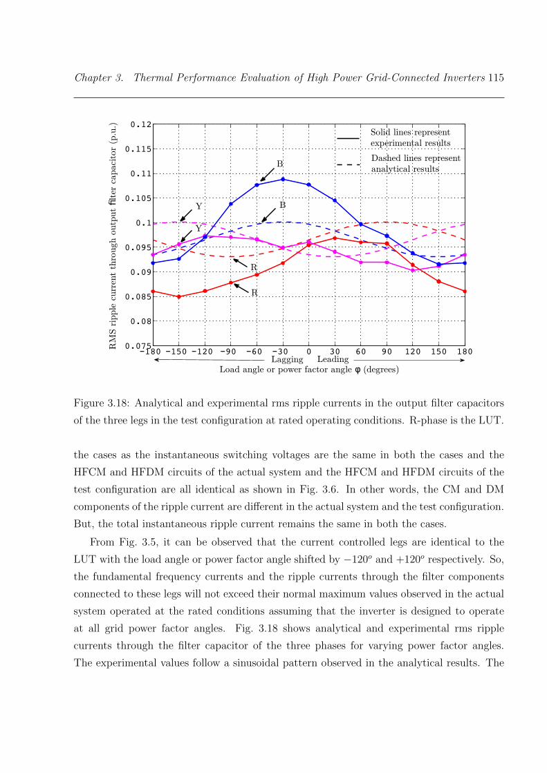
Chapter 3. Thermal Performance Evaluation of High Power Grid-Connected Inverters 115
−180 −150 −120 −90 −60 −30 0 30 60 90 120 150 1800.075
0.08
0.085
0.09
0.095
0.1
0.105
0.11
0.115
0.12
Load angle or power factor angle φ (degrees)
RMSripplecurrentthroughoutputfiltercapacitor(p.u.)
B
BY
R
R
Solid lines represent
experimental results
Dashed lines represent
analytical results
Y
LeadingLagging
Figure 3.18: Analytical and experimental rms ripple currents in the output filter capacitors
of the three legs in the test configuration at rated operating conditions. R-phase is the LUT.
the cases as the instantaneous switching voltages are the same in both the cases and the
HFCM and HFDM circuits of the actual system and the HFCM and HFDM circuits of the
test configuration are all identical as shown in Fig. 3.6. In other words, the CM and DM
components of the ripple current are different in the actual system and the test configuration.
But, the total instantaneous ripple current remains the same in both the cases.
From Fig. 3.5, it can be observed that the current controlled legs are identical to the
LUT with the load angle or power factor angle shifted by −120o and +120o respectively. So,
the fundamental frequency currents and the ripple currents through the filter components
connected to these legs will not exceed their normal maximum values observed in the actual
system operated at the rated conditions assuming that the inverter is designed to operate
at all grid power factor angles. Fig. 3.18 shows analytical and experimental rms ripple
currents through the filter capacitor of the three phases for varying power factor angles.
The experimental values follow a sinusoidal pattern observed in the analytical results. The

116 3.9. Analysis and Experimental Results – 3-Wire Configuration
differences in the p.u. rms values were observed to be of the same order as the tolerances of
the inductors used in the hardware. The variation in inductance is around 5%. This leads
to about 5% variation in the ripple current also.
3.9 Analysis and Experimental Results – 3-Wire Con-
figuration
In a 3-wire configuration, the fourth wire shown in dotted lines in Fig. 3.2 is disconnected.
Disconnecting the fourth wire changes only the CM currents. In the test configuration, the
fundamental frequency currents can still be maintained to be three-phase balanced and at
the rated value. But, since the voltages at the output terminals of the test configuration are
predominantly CM, the ripple is now very low compared to the 3-wire configuration of the
actual system. As discussed earlier, the effect of output ripple current on the thermal testing
of the semiconductor devices and the testing of the dc bus capacitors is negligible. Hence, the
thermal testing of the semiconductor devices and the dc bus capacitor testing can be done
for the 3-wire configuration as it was done for the 4-wire case. However, for the output filter
components, the test configuration emulates the actual system only at the fundamental
frequency. The high frequency losses in the output filter cannot be characterized for the
3-wire configuration. The tests for the 3-wire configuration are explained in the context
of space vector modulation scheme. The experimental results use the conventional space
vector pulse width modulation (CSVPWM) scheme at a dc bus voltage of 700 V. The dc
bus voltage has been reduced so as to have similar modulation indices for the sine-triangle
and CSVPWM schemes.
The modulating signal in space vector based PWM techniques can be seen as the sum
of a fundamental frequency sine wave modulating signal and a common mode modulating
signal. In particular, for the CSVPWM scheme, the common mode signal is half of the mid
value of the three sinusoidal references at any instant as shown in Fig. 3.19. The common
mode signal can be approximated using a triangular waveform of peak equal to one-fourth of
the peak of the sine waveform. The triangular waveform can further be approximated using
its fundamental frequency sine waveform. This approximated sine is shown in Fig. 3.19 and
is useful in the thermal analysis of the semiconductor devices. The approximated sine is a
third harmonic of the fundamental frequency sine wave modulating signals as can be observed
from the waveforms. Fig. 3.20 shows the actual and approximated CSVPWM modulating
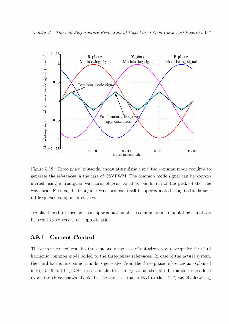
Chapter 3. Thermal Performance Evaluation of High Power Grid-Connected Inverters 117
0 0.005 0.01 0.015 0.02−1.25
−1
−0.5
0
0.5
1
1.25
Time in seconds
Modulatingsignalandcommonmodesignal(nounit)
R-phase Y phase B phase
Modulating signal
approximation
Modulating signal Modulating signal
Fundamental frequency
Common mode signal
Figure 3.19: Three-phase sinusoidal modulating signals and the common mode required to
generate the references in the case of CSVPWM. The common mode signal can be approx-
imated using a triangular waveform of peak equal to one-fourth of the peak of the sine
waveform. Further, the triangular waveform can itself be approximated using its fundamen-
tal frequency component as shown.
signals. The third harmonic sine approximation of the common mode modulating signal can
be seen to give very close approximation.
3.9.1 Current Control
The current control remains the same as in the case of a 4-wire system except for the third
harmonic common mode added to the three phase references. In case of the actual system,
the third harmonic common mode is generated from the three phase references as explained
in Fig. 3.19 and Fig. 3.20. In case of the test configuration, the third harmonic to be added
to all the three phases should be the same as that added to the LUT, say R-phase leg,
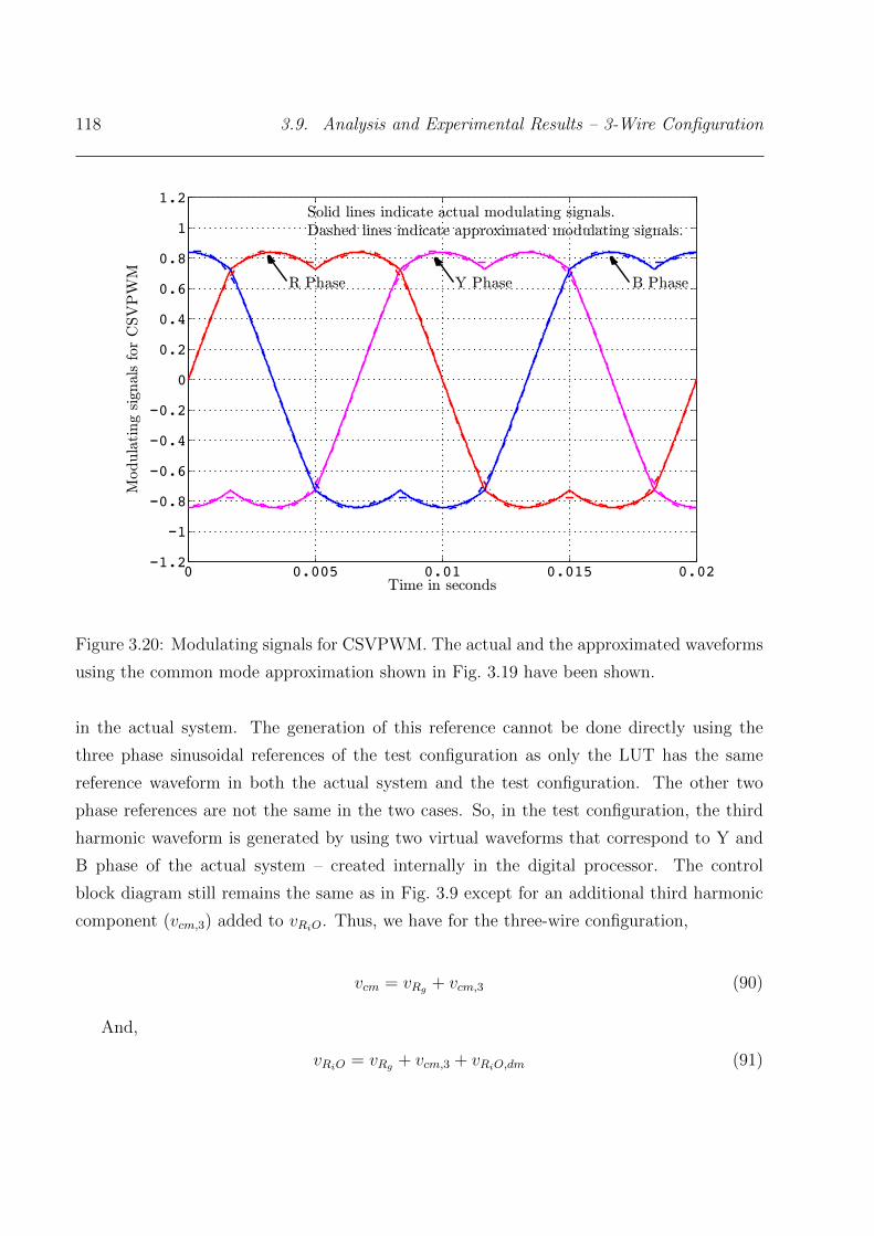
118 3.9. Analysis and Experimental Results – 3-Wire Configuration
0 0.005 0.01 0.015 0.02−1.2
−1
−0.8
−0.6
−0.4
−0.2
0
0.2
0.4
0.6
0.8
1
1.2
Time in seconds
ModulatingsignalsforCSVPWM
R Phase Y Phase B Phase
Solid lines indicate actual modulating signals.
Dashed lines indicate approximated modulating signals.
Figure 3.20: Modulating signals for CSVPWM. The actual and the approximated waveforms
using the common mode approximation shown in Fig. 3.19 have been shown.
in the actual system. The generation of this reference cannot be done directly using the
three phase sinusoidal references of the test configuration as only the LUT has the same
reference waveform in both the actual system and the test configuration. The other two
phase references are not the same in the two cases. So, in the test configuration, the third
harmonic waveform is generated by using two virtual waveforms that correspond to Y and
B phase of the actual system – created internally in the digital processor. The control
block diagram still remains the same as in Fig. 3.9 except for an additional third harmonic
component (vcm,3) added to vRiO. Thus, we have for the three-wire configuration,
vcm = vRg + vcm,3 (90)
And,
vRiO = vRg + vcm,3 + vRiO,dm (91)
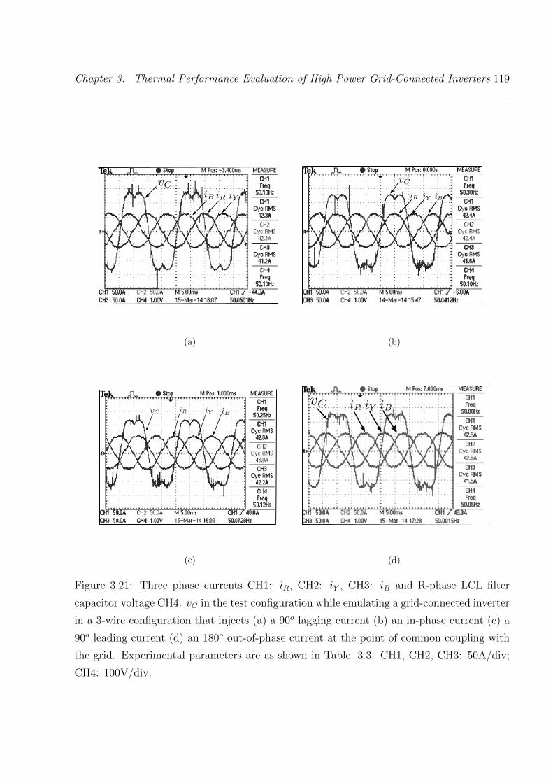
Chapter 3. Thermal Performance Evaluation of High Power Grid-Connected Inverters 119
(a) (b)
(c) (d)
Figure 3.21: Three phase currents CH1: iR, CH2: iY , CH3: iB and R-phase LCL filter
capacitor voltage CH4: vC in the test configuration while emulating a grid-connected inverter
in a 3-wire configuration that injects (a) a 90o lagging current (b) an in-phase current (c) a
90o leading current (d) an 180o out-of-phase current at the point of common coupling with
the grid. Experimental parameters are as shown in Table. 3.3. CH1, CH2, CH3: 50A/div;
CH4: 100V/div.
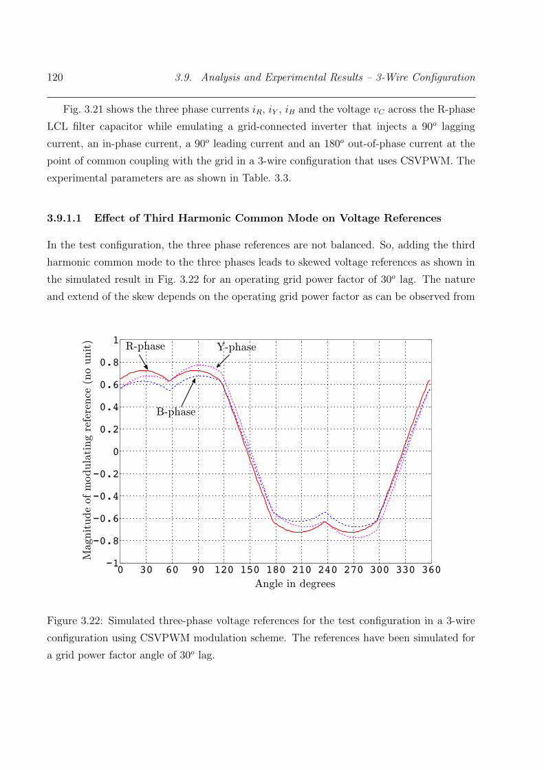
120 3.9. Analysis and Experimental Results – 3-Wire Configuration
Fig. 3.21 shows the three phase currents iR, iY , iB and the voltage vC across the R-phase
LCL filter capacitor while emulating a grid-connected inverter that injects a 90o lagging
current, an in-phase current, a 90o leading current and an 180o out-of-phase current at the
point of common coupling with the grid in a 3-wire configuration that uses CSVPWM. The
experimental parameters are as shown in Table. 3.3.
3.9.1.1 Effect of Third Harmonic Common Mode on Voltage References
In the test configuration, the three phase references are not balanced. So, adding the third
harmonic common mode to the three phases leads to skewed voltage references as shown in
the simulated result in Fig. 3.22 for an operating grid power factor of 30o lag. The nature
and extend of the skew depends on the operating grid power factor as can be observed from
0 30 60 90 120 150 180 210 240 270 300 330 360−1
−0.8
−0.6
−0.4
−0.2
0
0.2
0.4
0.6
0.8
1
Angle in degrees
Magnitudeofmodulatingreference(nounit)
Y-phaseR-phase
B-phase
Figure 3.22: Simulated three-phase voltage references for the test configuration in a 3-wire
configuration using CSVPWM modulation scheme. The references have been simulated for
a grid power factor angle of 30o lag.

Chapter 3. Thermal Performance Evaluation of High Power Grid-Connected Inverters 121
−0.02 −0.01 0 0.01 0.02−1
−0.75
−0.5
−0.25
0
0.25
0.5
0.75
1
Time in s
Modulatingreferences(nounit) R Phase
Y Phase
B Phase
(a)
−0.02 −0.01 0 0.01 0.02−1
−0.75
−0.5
−0.25
0
0.25
0.5
0.75
1
Time in sModulatingreferences(nounit)
B Phase
R Phase Y Phase
(b)
−0.02 −0.01 0 0.01 0.02−1
−0.75
−0.5
−0.25
0
0.25
0.5
0.75
1
Time in s
Modulatingreferences(nounit) Y Phase
B Phase
R Phase
(c)
Figure 3.23: Experimental three-phase skewed voltage references in the test configuration
for CSVPWM at (a) 90o lagging grid power factor (b) unity grid power factor (c) 90o leading
grid power factor. The experimental conditions are as mentioned in Table. 3.3. R-phase leg
is the LUT. The modulating signals have been scaled to -1 V to +1 V, the usual range used
in a triangle comparison method of gate signal generation.

122 3.9. Analysis and Experimental Results – 3-Wire Configuration
the experimental waveforms shown in Fig. 3.23 for 90o lagging current, an in-phase current
and a 90o leading current. As can be seen, the reference voltages for the legs other than
the LUT might have peak magnitudes greater than the peak magnitude observed in the
actual system. This means that the modulation indices might be pushed to their limits
when operated under the suggested test configuration.
The left Y axis of Fig. 3.24 shows the plot of the simulated peaks of the three-phase mod-
ulating references in the actual system and the test configuration for a 3-wire configuration
operated using CSVPWM at various grid power factor angles. The various parameters used
for simulation appear in Table. 3.3. The right Y axis shows the plot of percentage of modula-
−150 −100 −50 0 50 100 1500
0.2
0.4
0.6
0.8
1
Grid power factor angle (degrees)
Maxim
um
valueofthemodulatingreferences(nounit)
-180 1800
10
20
30
40
50
60
70
80
90
100
110
120
Percentageofmodulatingreference
peak
Test configuration
Actual system
At individual operating power factors (right Y axis)
When operated at entire power factor range
(right Y axis)
Figure 3.24: Y1 axis (left Y axis): Modulation peak at different operating grid power factors
for the actual system (solid line) and the test configuration (dashed line). Y2 axis (right Y
axis): Percentage of modulation peak for the test configuration as compared to that of the
actual system when operated at different grid power factors (dashed line) and when designed
for the entire grid power factor range (solid line). The plots are the simulated results for the
parameters given in Table. 3.3.

Chapter 3. Thermal Performance Evaluation of High Power Grid-Connected Inverters 123
tion peak in the test configuration in comparison with that of the actual system at different
grid power factor angles. As can be observed, the percentage increase in peak modulation
depends on the operating grid power factor angle and can be as high as 14.8% corresponding
to a grid power factor angle of 90o lead. From the perspective of dc bus requirement, this
means that when designed for operation only at 90o lead, the ideal minimum dc bus voltage
requirement is 456V for the actual system whereas to run the proposed test, a minimum dc
bus voltage of 524V i.e. an increase of 68V is required. However, if the inverter is designed
for the entire range of grid power factors, the percentage increase in peak modulation is less
at 4.7%. This means that the minimum dc bus requirement in the actual system and the
test configuration are 524V and 549V respectively i.e. an increase of only 25V is required.
In most practical cases, the dc bus voltage might be sufficient to run the test using the
proposed test configuration even when the inverter is designed to operate at particular grid
power factor.
3.9.2 Thermal Testing of Semiconductor Devices
The closed-form expressions for the switching loss in the IGBTs and diodes and the module
terminal losses are the same for sine triangle and CSVPWM schemes. Only the conduction
losses differ with the PWM scheme. Closed-form expressions for conduction loss in the IGBT
and diode can be arrived at in case of CSVPWM scheme by approximating the common
mode by a triangular waveform and by considering only the fundamental component of the
triangular common mode. The expressions are given in Appendix E. This approximation
would give very close results to that obtained using the exact common mode component as
the voltage references generated by the approximation are very close to the exact references
as can be observed from Fig. 3.20. Further, the total loss itself is not very different from
the total loss obtained for a sine triangle PWM scheme with the same dc bus voltage as
shown in Fig. 3.25. So, the variation of the loss per leg in the actual system and the test
configuration with the grid power factor angle can be approximated using a sine function
P (φ) = Po + Pmsin(φ − 90o) as in Section 3.8.2 as the effect of third harmonic terms of
power loss is negligible as can be observed from Fig. 3.25. The maximum percentage error
in the total loss of the test configuration as compared to that of the actual system is 0.51%.
Hence, the proposed test method is useful for thermal testing of semiconductor devices in
case of 3-wire also.
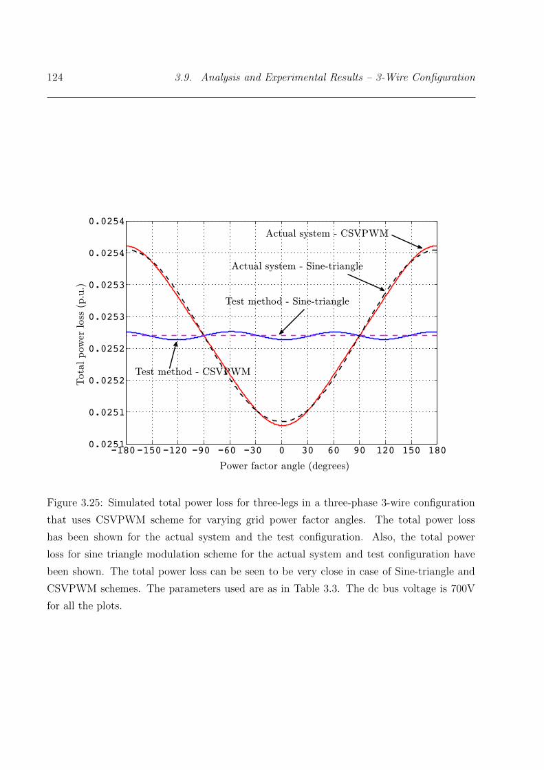
124 3.9. Analysis and Experimental Results – 3-Wire Configuration
−180−150−120 −90 −60 −30 0 30 60 90 120 150 1800.0251
0.0251
0.0252
0.0252
0.0253
0.0253
0.0254
0.0254
Power factor angle (degrees)
Totalpowerloss(p.u.)
Actual system - CSVPWM
Actual system - Sine-triangle
Test method - Sine-triangle
Test method - CSVPWM
Figure 3.25: Simulated total power loss for three-legs in a three-phase 3-wire configuration
that uses CSVPWM scheme for varying grid power factor angles. The total power loss
has been shown for the actual system and the test configuration. Also, the total power
loss for sine triangle modulation scheme for the actual system and test configuration have
been shown. The total power loss can be seen to be very close in case of Sine-triangle and
CSVPWM schemes. The parameters used are as in Table 3.3. The dc bus voltage is 700V
for all the plots.
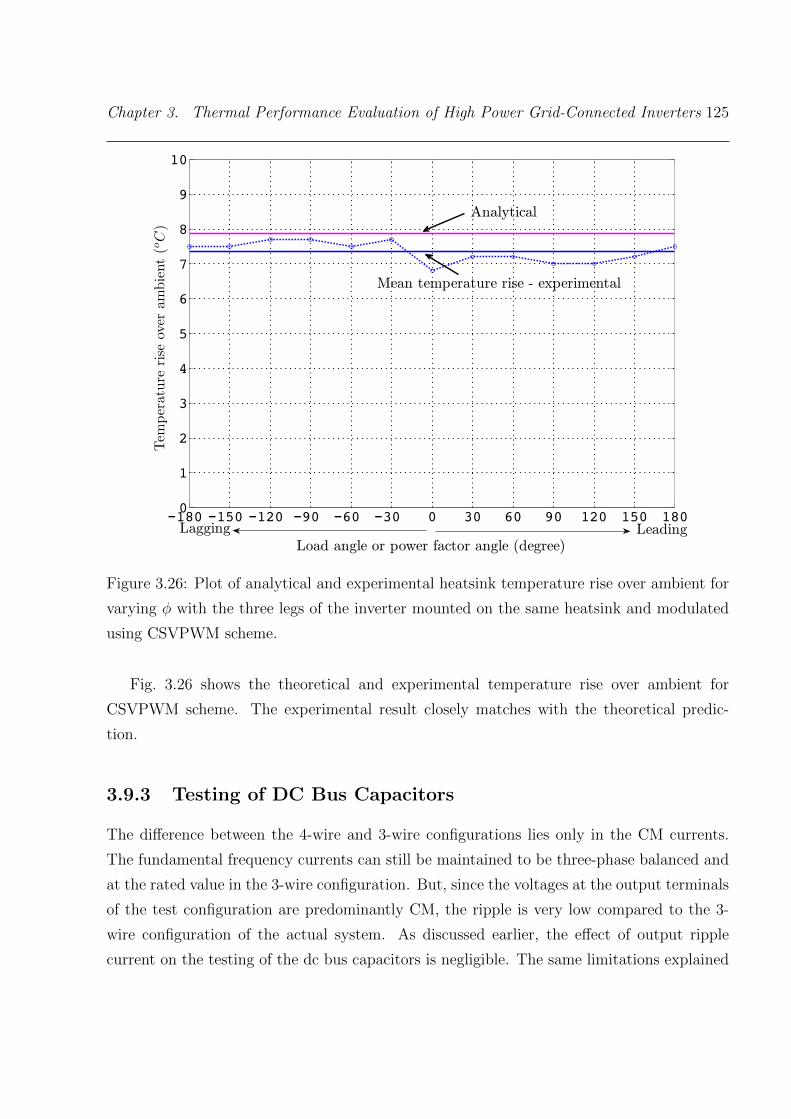
Chapter 3. Thermal Performance Evaluation of High Power Grid-Connected Inverters 125
−180 −150 −120 −90 −60 −30 0 30 60 90 120 150 1800
1
2
3
4
5
6
7
8
9
10
Load angle or power factor angle (degree)
Analytical
Mean temperature rise - experimental
LeadingLagging
Figure 3.26: Plot of analytical and experimental heatsink temperature rise over ambient for
varying φ with the three legs of the inverter mounted on the same heatsink and modulated
using CSVPWM scheme.
Fig. 3.26 shows the theoretical and experimental temperature rise over ambient for
CSVPWM scheme. The experimental result closely matches with the theoretical predic-
tion.
3.9.3 Testing of DC Bus Capacitors
The difference between the 4-wire and 3-wire configurations lies only in the CM currents.
The fundamental frequency currents can still be maintained to be three-phase balanced and
at the rated value in the 3-wire configuration. But, since the voltages at the output terminals
of the test configuration are predominantly CM, the ripple is very low compared to the 3-
wire configuration of the actual system. As discussed earlier, the effect of output ripple
current on the testing of the dc bus capacitors is negligible. The same limitations explained
126 3.10. Summary
in Section 3.8.3 apply for the 3-wire case also. Hence, the dc bus capacitor testing can be
done for the 3-wire configuration as it was done for the 4-wire case.
3.9.4 Testing of Output Filter Components
As explained in Section 3.9.3, the ripple is very low in the test configuration as compared
to the actual system in a 3-wire configuration. So, for the output filter components, the
test configuration emulates the actual system only at the fundamental frequency. The high
frequency losses in the output filter cannot be characterized for the 3-wire configuration.
3.10 Summary
In this Chapter a new test method to evaluate the thermal performance of the semiconduc-
tor devices of a high-power three-phase grid-connected inverter with output LCL filter is
described. The proposed method does not require a high power source or load. The power
taken from the grid supplies only the losses in the system under test. Compared to the other
power circulation methods available in literature which use another inverter of the same
rating, the power consumption is reduced by nearly 50% as the rated currents are circulated
within the same inverter in the proposed method. Further, the method can be used for
thermal testing of the semiconductor devices in either case of the cooling arrangement being
common or independent for the individual semiconductor devices or legs of the inverter. The
proposed method has been analyzed in detail for a three-phase 4-wire configuration. The
control method of the test configuration has been discussed. The usefulness of the method
to test the dc bus capacitors and output filter components has been studied. The procedures
for the semiconductor device thermal test, dc bus capacitor testing and output filter com-
ponents testing have been elaborated and the equivalence of the test methods to the actual
system have been shown. The total power loss in the proposed test method is shown to differ
from that of the actual system by 0.5% to 1.05% only, for a switching frequency range of 2.5
kHz to 10 kHz. The dc bus capacitor can be tested upto around 70% of its highest expected
rms current. For a 3-wire case, the test configuration is seen to emulate the output filter
component currents only at the fundamental frequency. The applicability of the method to
space vector based PWM techniques has also been shown. Experimental results from the
inverter operated at 24 kVA have been used to validate the proposed test approach. This

Chapter 3. Thermal Performance Evaluation of High Power Grid-Connected Inverters 127
test method has a wide practical applicability in testing of high power inverters.

128 3.10. Summary

Chapter 4
Control Performance Evaluation of
Grid-Connected Inverters
In recent years, renewable sources integrated to the grid are on the increase. Renewable
sources invariably use a grid-connected inverter as an interface to the grid. With the power
levels of wind and solar generation units having reached a few MWs, a sudden disconnection
of these renewable sources due to short time grid disturbances such as voltage sags and
voltage swells can cause instability in the grid. To avoid this, regulations mandate high
power wind and solar generation units to have Low Voltage Ride-Through (LVRT) and High
Voltage Ride-Through (HVRT) capabilities. LVRT and HVRT capabilities are additional
controls implemented in the grid-connected inverters to stay connected to the grid during
prescribed depths and durations of voltage sags and voltage swells respectively. To test
these capabilities before commissioning, it is required to re-create short time disturbances
like voltage sags and voltage swells in the testing laboratory. A hardware grid simulator can
be used for this. The present day hardware grid simulators are usually inverters that are
controlled to emulate the disturbances usually observed in the grid.
Besides useful for LVRT and HVRT testing, a grid simulator can be used to test any elec-
trical equipment connected to a low voltage grid for its adherence to the EMI standard IEC
61000-4-11 [68]/IEC 61000-4-34 [69]. IEC 61000-4-11/IEC 61000-4-34 gives recommended
immunity tests – for equipment connected to the mains – towards voltage dips, short in-
terruptions and voltage variations. Further, the grid simulator can also be used to test the
controls of a grid-connected inverter like the current control and dc bus voltage control or
the performance of any other equipment connected to the grid under several real-time grid
conditions. A 50 kVA inverter has been programmed as a grid simulator to primarily test
the control performance of grid-connected inverters under various disturbance conditions.
129
130 4.1. Grid Simulators - A Survey
The developed grid simulator is capable of generating a wide range of disturbance conditions
– voltage sags, voltage swells, frequency deviation and phase jumps. This Chapter focuses
on the development of a simple yet effective algorithm to generate the different disturbance
conditions. The simulator has been experimentally tested with three-phase purely resistive,
diode-bridge and inverter loads.
Section 4.1 discusses the various methods available in literature to simulate the distur-
bances usually observed in the grid. The features of grid simulation products that have
recently become commercially available is also discussed. Further, the focus of the present
work is detailed. In Section 4.2, the topology of the grid simulator developed to test the
control performance of grid-connected inverters is briefed. Section 4.3 outlines the controls
used in the front-end converter and the output inverter. Section 4.4 explains the start-up
sequence of the grid-simulator inverters and the different modes involved in the generation
of a disturbance voltage. The Finite State Machine model for the control algorithm is de-
veloped in Section 4.5. Section 4.6 gives the details of the system parameters of the grid
simulator and the parameters of the different loads which are used to test the grid simulator’s
performance. The experimental results appear in Section 4.7. The scope for future work on
the grid simulator control to improve stiffness of the grid simulator output voltage is detailed
in Section 4.8. Section 4.9 summarises the work done on grid simulator.
4.1 Grid Simulators - A Survey
4.1.1 Grid Simulation Methods Available in Literature
The simulation of grid disturbances in a laboratory environment has been of interest for a
long time. However, till a few years back, the interest has primarily been to test for EMI
compliance as per the IEC standards IEC 61000-4-11 [68]/IEC 61000-4-34 [69] for electrical
equipment connected to the grid. Since the mentioned standards focus primarily on testing
of grid connected equipment under voltage sags, most earlier literature have limited their
focus to generation of voltage sags. All these earlier works [88, 109–111] mostly use simple
passive components [88, 109, 110] to create voltage sags with the exception of [111] which
uses a series-injected inverter for the same purpose. While [109] creates the sag by dropping
a desired fraction of the grid voltage across an inductor, [88] uses an auto-transformer tap
as a means to achieve the same. Both [109] and [88] use power electronic switches. In [109],
Chapter 4. Control Performance Evaluation of Grid-Connected Inverters 131
the load is attached to the grid through an inductor. A thyristor controlled reactor (TCR)
is connected in parallel to the load. Whenever a sag is required, the TCR is switched in a
controlled manner so that the current through the inductor increases and creates the sag of
required depth and duration. In [88], a power electronic switch is used to switch between
taps in the auto-transformer which creates a voltage sag at the output. [110] controls a syn-
chronous generator in closed loop to create a sag. In [111], a sag is created by injecting a
voltage in series with the grid using an inverter. The operating principle in [111] is similar to
that of a Dynamic Voltage Restorer (DVR) discussed in Section 1.1.1.1. The main drawback
of the above methods is that they are limited to creating only sags. Further, except for [111],
the other methods use passive components which are bulky, costly and lead to slow dynamic
excitation for creating the disturbance voltage.
With the distributed generation gaining pace and their power levels reaching a few MWs, re-
search work on grid simulators have become more generic in recent years [83–88]. The recent
literature aims at the generation of swells, unbalance, harmonic voltages and frequency devi-
ations apart from the sags. The requirement of a generic hardware has prompted researchers
to use IGBT based inverters. The hardware usually has an active front-end converter that
charges the dc bus and an inverter at the output side to generate the required grid dis-
turbances. The decoupled control of the front-end and output inverters together with the
bi-directional power flow capability of this topology makes it possible to generate a wide
range of grid disturbance conditions in the laboratory. The primary difference in the various
methods available in literature [83–88] is the topology used for the output inverter. The
front-end converter is a three-phase three-wire inverter in most cases [83–86]. For the output
inverter, [83] uses a three-phase 4-wire inverter with mid point dc bus connection while [86,87]
use a three-phase four-leg inverter and the rest [84, 85, 88] use a simple three-phase 3-wire
inverter. Reference [84] gives extensive experimental results for the developed grid simula-
tor hardware. The other literature discusses experimental results for only sags [83, 88] or
provide results only under open circuit condition of the output inverter without connecting
any loads [86, 87]. All above methods use already existing standard inverter topologies and
inverter control methods for the front-end converter and the output inverter. Hence, they all
are capable of producing disturbance conditions with comparable output voltage dynamics.

132 4.1. Grid Simulators - A Survey
4.1.2 Commercially Available Grid Simulators
Several manufacturers have recently introduced commercial grid simulator products. Ta-
ble 4.1 lists and compares the features of some commercially available grid simulators. The
primary objective of these systems are to test equipment for compliance to grid-connection
standards.
4.1.3 Focus of Work
As in recent literature, the present work also makes use of back-to-back connected inverters
sharing a common dc bus to generate grid disturbances. Inverter topologies and control
methods having become standard over the years, the work focuses mainly on developing a
simple yet effective control algorithm for generating the grid disturbances. A Moore Model
based Finite State Machine (FSM) [112] has been used to develop, analyse and implement the
algorithm in a digital controller. Using the proposed algorithm, the disturbance generation
can be referenced to any of the three phases at any desired phase angle. Further, by adjusting
the disturbance duration, the exit phase angle can be set as desired and can be referenced
to any of the three phases. The digital control makes it possible to control the point of
disturbance very close to the desired phase angle. Also, the algorithm allows the user to
repeat the disturbance creation any number of times without restarting the grid simulator,
by using a press button switch.
The developed grid simulator is capable of generating voltage sags, voltage swells, fre-
quency deviations and phase jumps. The focus of the work is to develop the grid simulator
as a test set-up to evaluate the control performance of grid-connected inverters. So, the
experimental studies are directed at testing the grid simulator’s capability to produce and
maintain the required voltage at its output terminals. Results have been provided to show
the various features of the implemented algorithm. The grid simulator has been tested with
different loads – a linear purely resistive load, a non-linear three-phase diode bridge load
and an inverter load. So, though the grid simulator is primarily built to test grid-connected
inverters, loads other than inverters can also be tested.
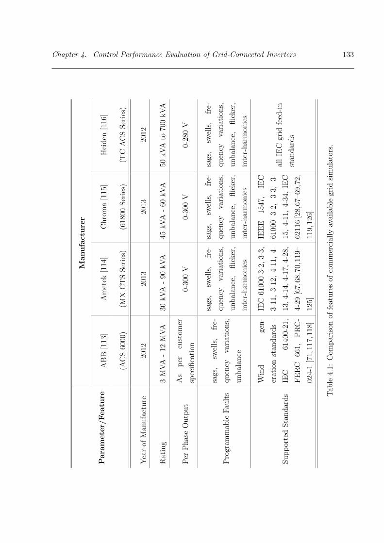
Chapter 4. Control Performance Evaluation of Grid-Connected Inverters 133
Para
mete
r/Featu
re
Manufa
cture
r
AB
B[1
13]
Am
etek
[114
]C
hro
ma
[115
]H
eiden
[116
]
(AC
S60
00)
(MX
CT
SSer
ies)
(618
00Ser
ies)
(TC
AC
SSer
ies)
Yea
rof
Man
ufa
cture
2012
2013
2013
2012
Rat
ing
3M
VA
-12
MV
A30
kV
A-
90kV
A45
kV
A-
60kV
A50
kV
Ato
700
kV
A
Per
Phas
eO
utp
ut
As
per
cust
omer
spec
ifica
tion
0-30
0V
0-30
0V
0-28
0V
Pro
gram
mab
leF
ault
s
sags
,sw
ells
,fr
e-
quen
cyva
riat
ions,
unbal
ance
sags
,sw
ells
,fr
e-
quen
cyva
riat
ions,
unbal
ance
,flic
ker,
inte
r-har
mon
ics
sags
,sw
ells
,fr
e-
quen
cyva
riat
ions,
unbal
ance
,flic
ker,
inte
r-har
mon
ics
sags
,sw
ells
,fr
e-
quen
cyva
riat
ions,
unbal
ance
,flic
ker,
inte
r-har
mon
ics
Supp
orte
dSta
ndar
ds
Win
dge
n-
erat
ion
stan
dar
ds
-
IEC
6140
0-21
,
FE
RC
661,
PR
C-
024-
1[7
1,11
7,11
8]
IEC
6100
03-
2,3-
3,
3-11
,3-
12,
4-11
,4-
13,
4-14
,4-
17,
4-28
,
4-29
[67,
68,7
0,11
9–
125]
IEE
E15
47,
IEC
6100
03-
2,3-
3,3-
15,
4-11
,4-
34,
IEC
6211
6[2
8,67
–69,
72,
119,
126]
all
IEC
grid
feed
-in
stan
dar
ds
Tab
le4.
1:C
ompar
ison
offe
ature
sof
com
mer
cial
lyav
aila
ble
grid
sim
ula
tors
.

134 4.2. Grid Simulator Topology
d
To Equipment Under Test
Fro
nt
End C
onver
ter
Outp
ut
Inver
ter
Gri
d
O
C
Fig
ure
4.1:
Gri
dSim
ula
tor
Top
olog
y.T
he
fron
t-en
dco
nve
rter
isa
thre
e-phas
ein
vert
erco
nnec
ted
toth
egr
idth
rough
anL
filt
er.
The
outp
ut
inve
rter
isa
thre
e-phas
ein
vert
erco
nfigu
rable
asa
3-w
ire
connec
tion
show
nin
solid
lines
or
asa
4-w
ire
wit
hdc
bus
mid
-poi
nt
connec
tion
show
nin
das
hed
lines
.A
LC
filt
eris
use
dto
filt
erth
esw
itch
ing
ripple
com
pon
ent
atth
eou
tput.
Pas
sive
resi
stiv
edam
pin
g(R
d)
isuse
dto
dam
pth
ere
sonan
ceof
the
LC
filt
er.

Chapter 4. Control Performance Evaluation of Grid-Connected Inverters 135
4.2 Grid Simulator Topology
Fig. 4.1 shows the topology used in the present work. As shown in the figure, the grid
simulator uses an IGBT based back-to-back connected inverter sharing a common dc bus.
The front-end uses a three-phase inverter with output L filter to connect to the grid. The
front-end converter ensures a fixed voltage at the common dc bus. At the output side, a
three-phase inverter with LC filter configurable in a 3-wire or 4-wire topology is used. The
output inverter is programmed to generate a wide range of disturbance conditions. The LC
filter resonance is damped by passive means through resistors (Rd) connected in series with
the output filter capacitors. The front-end converter and the output inverter are both rated
at 50 kVA. For the experiments, two legs of the front-end converter are used in a single-phase
configuration and hence the input rating is limited to 16.7 kVA.
4.3 Grid Simulator Controls
As explained in Section 4.2, the developed grid simulator has a front-end converter (FEC)
and an output inverter. The control of the FEC and the output inverter are decoupled.
The FEC tries to maintain a fixed dc bus voltage irrespective of the dynamics of the output
inverter. The output inverter uses the fixed dc bus voltage to create the required nominal
and disturbance voltages at its load terminals. Section 4.3.1 and Section 4.3.2 explain the
controls used for the FEC and output inverter respectively.
4.3.1 Front-End Converter Control
As explained in Section 4.2, the FEC is a single-phase grid-connected inverter with L filter.
The FEC locks to the grid using a Synchronous Reference Frame based Phase-Locked Loop
(SRF-PLL) [127]. The SRF-PLL requires transformation of the input grid voltage from
the stationary reference frame to the synchronous rotating d-q frame. The Second Order
Generalised Integrator (SOGI) [128] is used to convert the single phase input grid voltage
into orthogonal components to be used for dq transformation. Fig. 4.2 shows the SRF-PLL.
Once locked to the grid, the FEC uses an inner current control loop to draw near unity
power factor current from the grid. An outer dc bus voltage control loop maintains the
dc bus at the required reference voltage. The current loop uses a proportional-resonant
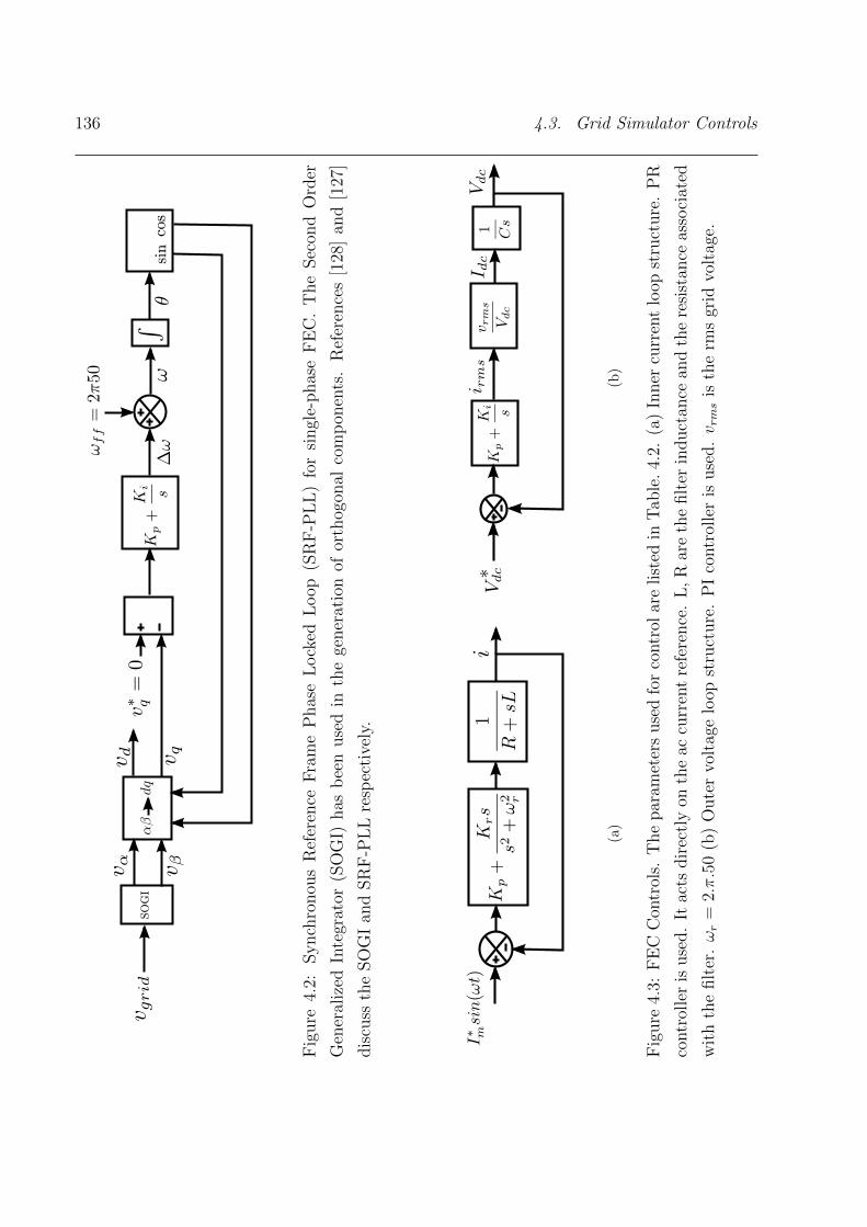
136 4.3. Grid Simulator Controls
sincos
SOGI
Fig
ure
4.2:
Synch
ronou
sR
efer
ence
Fra
me
Phas
eL
ock
edL
oop
(SR
F-P
LL
)fo
rsi
ngl
e-phas
eF
EC
.T
he
Sec
ond
Ord
er
Gen
eral
ized
Inte
grat
or(S
OG
I)has
bee
nuse
din
the
gener
atio
nof
orth
ogon
alco
mp
onen
ts.
Ref
eren
ces
[128
]an
d[1
27]
dis
cuss
the
SO
GI
and
SR
F-P
LL
resp
ecti
vely
.
(a)
(b)
Fig
ure
4.3:
FE
CC
ontr
ols.
The
par
amet
ers
use
dfo
rco
ntr
olar
elist
edin
Tab
le.
4.2.
(a)
Inner
curr
ent
loop
stru
cture
.P
R
contr
olle
ris
use
d.
Itac
tsdir
ectl
yon
the
accu
rren
tre
fere
nce
.L
,R
are
the
filt
erin
duct
ance
and
the
resi
stan
ceas
soci
ated
wit
hth
efilt
er.ωr
=2.π.5
0(b
)O
ute
rvo
ltag
elo
opst
ruct
ure
.P
Ico
ntr
olle
ris
use
d.v rms
isth
erm
sgr
idvo
ltag
e.

Chapter 4. Control Performance Evaluation of Grid-Connected Inverters 137
PLL Control Current Control Voltage Control
Parameter Value Parameter Value Parameter Value
Kp 0.775 rad/V -s Kp 125.6 V/A Kp 0.334 A/V
Ki 1.801 rad/V -s2 Kr 2543.7 V/A-s Ki 0.050 A/V -s
Table 4.2: FEC Control Parameters.
(PR) controller in the stationary reference frame for its control. The voltage loop uses a
proportional-integral (PI) controller. Fig. 4.3 shows the inner current control and outer
voltage control loops. The FEC uses sine-triangle modulation at a switching frequency of
10kHz.
Table. 4.2 lists the various control parameters used for the SRF-PLL, current and voltage
control loops.
4.3.2 Output Inverter Control
The output inverter is controlled as an open loop voltage source. The pulse-width modula-
tion signals are generated from the three-phase nominal and disturbance voltage references
using sine-triangle modulation at a switching frequency of 10kHz. The disturbance voltage
references are generated using the voltage disturbance generation algorithm explained in
Section 4.5.
4.4 Grid Simulator Operation
A proper start-up sequence is required to ensure that the grid simulator reaches a steady
operating state smoothly. The disturbance generation at the output inverter also requires a
well-defined sequence of operation. Section 4.4.1 and Section 4.4.2 explain the sequence of
operation of the grid simulator and the different modes involved in the generation of voltage
disturbance.

138 4.4. Grid Simulator Operation
4.4.1 Start-Up Sequence of Grid Simulator
The following is the start-up sequence of operation of the grid simulator once the input power
is switched on:
1. The anti-parallel diodes in the FEC act as a diode bridge rectifier and charge the dc
bus capacitor towards voltage V1. V1 corresponds to the diode bridge output voltage.
A resistor is connected in series with the filter inductor L when the dc bus starts to
charge. A contactor shorts out the resistor when the dc bus voltage is close to V1.
This ensures that the there are no current spikes due to sudden charging of dc bus
capacitor. The current control, dc bus voltage control and the output inverter controls
are not activated during this period. The gate pulses to both the inverters are withheld
through software.
2. When the anti-parallel diodes are charging the dc bus capacitor, the PLL control starts
and locks the inverter to the grid frequency and phase.
3. Once the dc bus is charged to V1, a toggle switch is used to start the current and
voltage loops of the FEC. The toggle switch action can be automated. The output
inverter controls still remain deactivated. The FEC controls boost the voltage from V1
to the set reference voltage, V ∗dc.
4. Once the dc bus voltage stabilises at V ∗dc, the output inverter control is activated using
a press button switch. This slowly ramps up the voltage at the ac terminals of the
output inverter to the nominal value. This ensures that there are no current spikes or
oscillations due to sudden charging of the output LC filter.
4.4.2 Modes during Disturbance Generation
Fig. 4.4 shows the different modes involved in the disturbance voltage generation at the ac
terminals of the output inverter including the start-up voltage ramp-up. The voltage mag-
nitude versus time plot has been drawn assuming the disturbance is a voltage sag. However,
the different modes shown are equally applicable to the other types of disturbances also.
The different modes are as follows:

Chapter 4. Control Performance Evaluation of Grid-Connected Inverters 139
Time (s)
Voltage
magnitude
(V)
Mode 1
Mode
0
Mode
3
Mode
2
Mode
4
Mode
5
Mode
6
Mode
2
Dis
turb
ance
Tri
gger
ed
Dis
turb
ance
Ends
indicates
time lapseV
V
Figure 4.4: Grid Simulator modes during voltage disturbance generation. tidle is the dura-
tion of idle state between successive disturbances, tdis is the time duration of the voltage
disturbance. Vnom, Vdis indicate the nominal and disturbance voltage magnitudes.
Mode 0: No output voltage
During this mode, the input power to the grid simulator has been switched on and the
grid simulator is going through its start-up sequence to boost the dc bus voltage to the set
reference, V ∗dc. The grid simulator output voltage is withheld during this mode as explained
in Section 4.4.1.
Mode 1: Voltage ramp-up
This mode is entered by activating a press button switch after ensuring that the dc bus
voltage has stabilised at V ∗dc. On pressing the switch, the output voltage of the grid simulator
ramps up slowly to the nominal value. The ramp up time is programmable.
Mode 2: Wait state between disturbances
This mode is entered once the output voltage is ramped up to the nominal value. The

140 4.4. Grid Simulator Operation
grid simulator enters into a wait state for a set interval of time. During the wait state, the
disturbance event cannot be triggered. The grid simulator has been programmed to re-create
a disturbance any number of times to allow the user to repeat the test to study different
control behaviour of the equipment under test without having to restart the grid simulator.
Since the same press button switch is used to create the disturbance several times, a wait
time is provided between successive disturbances so as to avoid false triggers.
Mode 3: Ready state
This mode is entered once the wait time between successive faults elapse. The output
voltage remains at the nominal value. The grid simulator is ready to service any disturbance
trigger input. The ready state is exited on triggering a disturbance using the press button
switch.
Mode 4: Wait state for end of current cycle of reference phase
This mode is entered on receiving the trigger to start the disturbance. The algorithm
waits for the end of the current cycle of the reference phase so that the disturbance can be
started at the required phase angle in the new cycle. The output ac voltage is at its nominal
value during this mode.
Mode 5: Wait state for desired phase angle in new cycle
This mode is entered on the completion of the current cycle of the reference phase after
the disturbance is triggered using the press button switch. The algorithm monitors the phase
angle of the reference phase during this mode. The mode ends when the desired phase angle,
θ∗ is reached. The output ac voltage is at its nominal value during this mode.
Mode 6: Disturbance state
This mode is entered on the phase angle of the reference phase reaching the desired
value. The disturbance voltage appears at the output ac terminals during this mode. The
three phase disturbance voltage magnitude, frequency and starting phase are programmable.
Magnitude setting helps create a sag, swell or unbalance, frequency deviations are created
by adjusting the frequency setting, starting phase can be used to create phase jumps. A
combination of different settings can help create a wide range of disturbance conditions. The
duration of this mode is programmable. By adjusting the duration of the disturbance, the
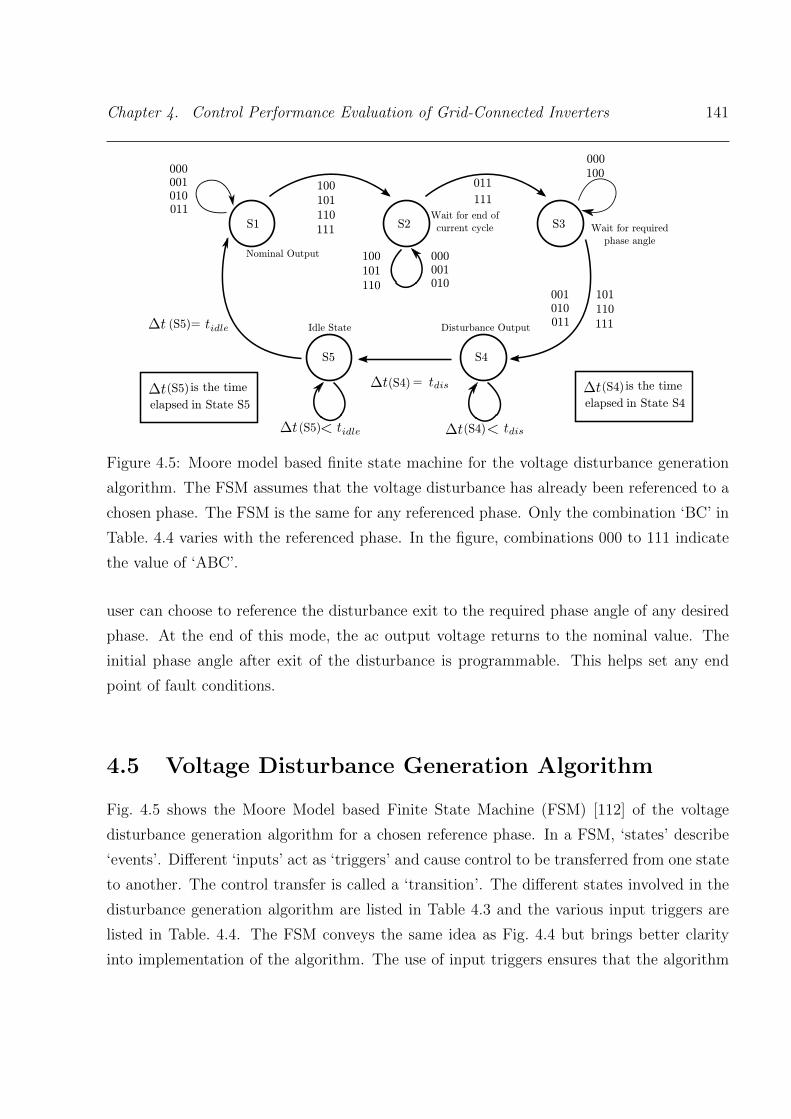
Chapter 4. Control Performance Evaluation of Grid-Connected Inverters 141
S1 S2 S3
S4S5
Idle State
Nominal Output
Disturbance Output
Wait for end of
current cycle Wait for required
phase angle
100
101
110
111
000001010011
111
011
000001010
100
101
110
000
101
110
111
001010011=
=
(S4)
(S4)
(S5)
(S5)
(S4) is the time
in State S4elapsed
(S5) is the time
in State S5elapsed
100
Figure 4.5: Moore model based finite state machine for the voltage disturbance generation
algorithm. The FSM assumes that the voltage disturbance has already been referenced to a
chosen phase. The FSM is the same for any referenced phase. Only the combination ‘BC’ in
Table. 4.4 varies with the referenced phase. In the figure, combinations 000 to 111 indicate
the value of ‘ABC’.
user can choose to reference the disturbance exit to the required phase angle of any desired
phase. At the end of this mode, the ac output voltage returns to the nominal value. The
initial phase angle after exit of the disturbance is programmable. This helps set any end
point of fault conditions.
4.5 Voltage Disturbance Generation Algorithm
Fig. 4.5 shows the Moore Model based Finite State Machine (FSM) [112] of the voltage
disturbance generation algorithm for a chosen reference phase. In a FSM, ‘states’ describe
‘events’. Different ‘inputs’ act as ‘triggers’ and cause control to be transferred from one state
to another. The control transfer is called a ‘transition’. The different states involved in the
disturbance generation algorithm are listed in Table 4.3 and the various input triggers are
listed in Table. 4.4. The FSM conveys the same idea as Fig. 4.4 but brings better clarity
into implementation of the algorithm. The use of input triggers ensures that the algorithm

142 4.5. Voltage Disturbance Generation AlgorithmSta
teD
esc
ripti
on
Corr
esp
ondin
g
Mode
Sta
te1
(S1)
Gri
dsi
mula
tor
outp
ut
volt
age
isat
its
nom
-
inal
valu
ean
daw
aits
adis
turb
ance
trig
ger
input.
Mode
3
Sta
te2
(S2)
Gri
dsi
mula
tor
wai
ts
for
the
curr
ent
cycl
eof
the
refe
rence
phas
eto
end
(θ=
360o
).
Mode
4
Sta
te3
(S3)
Gri
dsi
mula
tor
wai
ts
for
the
des
ired
phas
e
angl
e(θ
=θ∗
)to
be
reac
hed
for
the
refe
r-
ence
phas
e.
Mode
5
Sta
te4
(S4)
Dis
turb
ance
volt
age
is
crea
ted
atth
eou
tput.
Mode
6
Sta
te5
(S5)
Gri
dsi
mula
tor
isid
le.
No
dis
turb
ance
can
be
trig
gere
d.
Mode
2
Tab
le4.
3:D
escr
ipti
onof
Sta
tes
ofth
eF
SM
Pre
ssB
utt
on
Sw
itch
Sta
tus
Com
bin
ati
on
(A)
Sta
tus
0T
he
pre
ssbutt
onsw
itch
has
not
bee
n
pre
ssed
1T
he
pre
ssbutt
onsw
itch
has
bee
n
pre
ssed
Phase
an
gle
of
refe
ren
cep
hase
Com
bin
ati
on
(BC
)Sta
tus
000o<θ<θ∗
01θ
=θ∗
10θ∗<θ<
360o
11θ≥
360o
Tim
edu
rati
on
of
dis
turb
an
ce
t dis
Indic
ates
the
dura
tion
ofdis
turb
ance
.
Tim
edu
rati
on
of
idle
state
t idle
Indic
ates
the
dura
tion
ofid
lest
ate
be-
twee
nsu
cces
sive
dis
turb
ance
s.
Tab
le4.
4:T
rigg
erIn
puts
Chapter 4. Control Performance Evaluation of Grid-Connected Inverters 143
is tested for all possible combination of triggers, thus avoiding any mal-operation due to
unexpected input conditions. The FSM can be understood by comparing the different states
with Modes 2 to 6 discussed in Section 4.4. The modes corresponding to the different states
are listed in Table 4.3. The FSM has been drawn assuming a reference phase to have been
chosen already. For different selections of reference phase, only the phase angle used for
generating trigger combinations ‘BC’ will change.
4.6 Grid Simulator Parameters and Test Loads
The grid simulator hardware is rated at 50kVA. Though the grid simulator is rated at
50kVA, it is expected to be used to test loads upto 10kVA only. The high margin is given
to ensure that the grid simulator works effectively even under unexpected fault conditions
of the connected load during testing. Further, the experiments have been conducted at a
lower power level. For the experiments, the dc bus voltage is set to 500 V. The switching
frequency is 10 kHz for both the FEC and the output inverter. The nominal output voltage
per phase is 120V rms and the fundamental frequency is 50Hz. The filter inductor value for
the FEC is 20mH. The output inverter LC filter values are 5mH and 3µF. A 2Ω resistance
is connected in series with the LC filter capacitors to damp the LC resonance.
Fig. 4.6 and Fig. 4.7 show the linear purely resistive load, non-linear diode bridge load
and current-controlled inverter load used as test loads in the experimental studies. The
values of the various components used in the loads have been indicated in the figures. In
the diode bridge load, the inductors are used to smoothen the input currents and the output
capacitor is used to maintain a steady dc bus voltage. The inverter load is controlled as a
grid-connected STATCOM using current control implemented in the synchronous reference
(dq) frame [2]. The STATCOM uses a Synchronous Reference Frame Phase Locked Loop
(SRF-PLL) [127] to lock to the grid simulator’s output frequency and phase. The convention
used for the STATCOM considers d-axis to be aligned along the voltage vector and q-axis
to be lagging the d-axis by 90o i.e. a current along d-axis would indicate real current and a
current along q-axis would indicate a reactive current. The SRF-PLL generates a cos unit
vector along the d-axis and a sin unit vector along the q-axis for use in the current control.
As per the conventions used for the STATCOM, cos unit vector is in-phase with the R-phase
grid voltage and sin unit vector lags R-phase grid voltage by 90o.

144 4.6. Grid Simulator Parameters and Test Loads
R Y B
(a) (b)
Figure 4.6: Three-phase 3-wire loads used for experimental testing of the grid simulator. (a)
A linear purely resistive load. (b) A non-linear diode-bridge load.
O
5mH
5mH
5mH
Figure 4.7: A three-phase 3-wire inverter load used for experimental testing of the grid
simulator. The inverter is programmed as a current controlled STATCOM. The inverter is
rated for 10kVA and switches at 10kHz.
Chapter 4. Control Performance Evaluation of Grid-Connected Inverters 145
4.7 Experimental Results
4.7.1 Modes of Operation of Grid Simulator
Fig. 4.8 and Fig. 4.9 show the different modes in the voltage disturbance generation as
discussed in Section 4.4.2. Fig. 4.8 shows mode 0 and mode 1. There is no output voltage
from the grid simulator in mode 0. The voltage ramps up in mode 1. The slow ramping
up of voltage helps avoid capacitor current spikes at the output LC filter. Fig. 4.9(a) and
Fig. 4.9(b) show modes 2 to 6 for a 50% voltage sag of 5 cycles. The sag is referenced to
R-phase at an angle of 30o. In all the figures in this Section, the trigger status indicates the
point at which the disturbance is triggered and serviced. The trigger status goes from LOW
to HIGH when the disturbance is triggered using a press button switch. The trigger status
goes from HIGH to LOW when the disturbance is serviced i.e. when disturbance period
starts at the desired phase angle of the referenced phase.
4.7.2 Sag, Swell and Frequency Deviation
Fig. 4.10 shows DSP references for different types of faults. Voltage sag, voltage swell and fre-
quency deviation have been shown. An example of a phase jump is shown in Section 4.7.3.3.
4.7.3 Load Testing
The grid simulator has been tested with linear, non-linear and inverter loads. The experi-
mental results from the various tests are discussed in this Section.
4.7.3.1 Linear Purely Resistive Load
Fig. 4.11 shows the response of a linear purely resistive load to a 50% voltage sag created by
the grid simulator. The load current can be observed to immediately fall by 50% as expected
during the sag.
4.7.3.2 Non-Linear Diode-Bridge Load
Fig. 4.12 shows the response of a non-linear diode bridge load to a 50% voltage sag created
by the grid simulator. The load current can be observed to become zero on entering the
disturbance condition. Since the input voltage dips, for a few cycles the input current
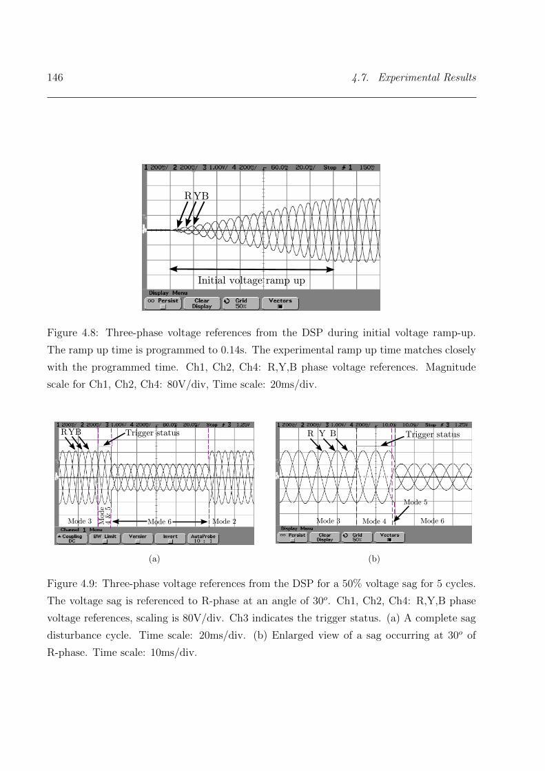
146 4.7. Experimental Results
Initial voltage ramp up
RYB
Figure 4.8: Three-phase voltage references from the DSP during initial voltage ramp-up.
The ramp up time is programmed to 0.14s. The experimental ramp up time matches closely
with the programmed time. Ch1, Ch2, Ch4: R,Y,B phase voltage references. Magnitude
scale for Ch1, Ch2, Ch4: 80V/div, Time scale: 20ms/div.
RYB Trigger status
Mode 2Mode 3 Mode
Mode 64 &
5
(a)
Mode 3 Mode 6Mode 4
Mode 5
R Y B Trigger status
(b)
Figure 4.9: Three-phase voltage references from the DSP for a 50% voltage sag for 5 cycles.
The voltage sag is referenced to R-phase at an angle of 30o. Ch1, Ch2, Ch4: R,Y,B phase
voltage references, scaling is 80V/div. Ch3 indicates the trigger status. (a) A complete sag
disturbance cycle. Time scale: 20ms/div. (b) Enlarged view of a sag occurring at 30o of
R-phase. Time scale: 10ms/div.
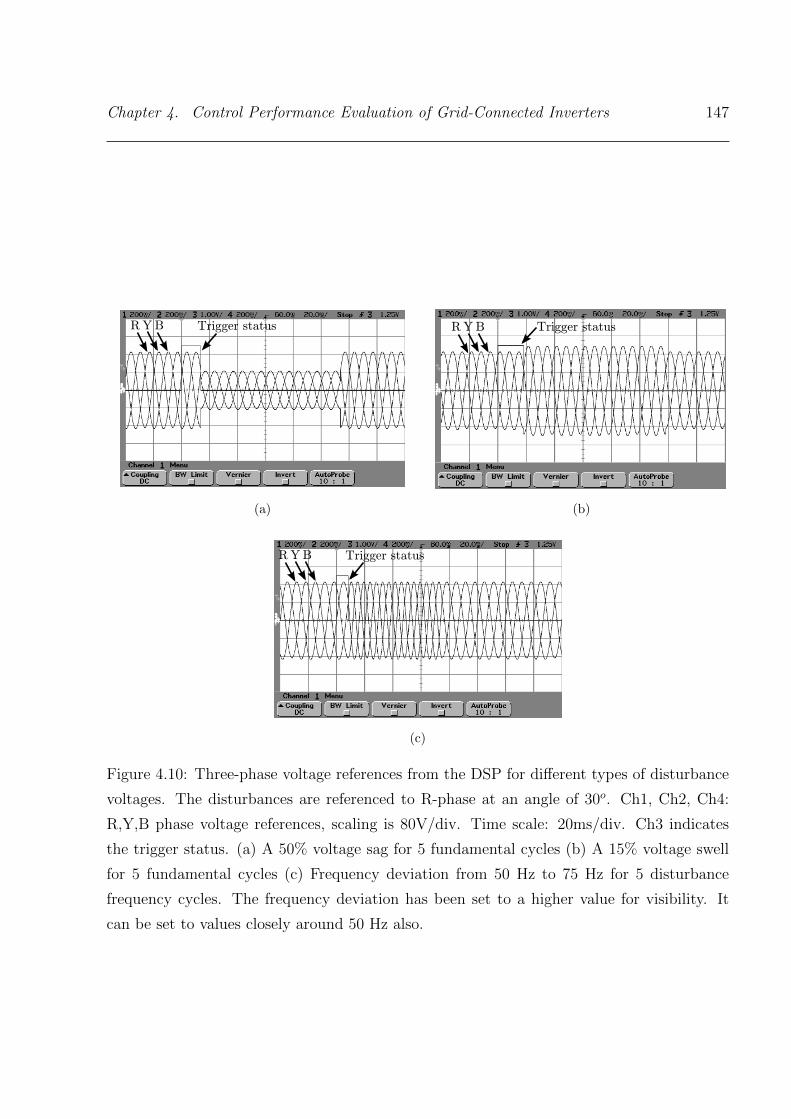
Chapter 4. Control Performance Evaluation of Grid-Connected Inverters 147
R Y B Trigger status
(a)
R Y B Trigger status
(b)
R Y B Trigger status
(c)
Figure 4.10: Three-phase voltage references from the DSP for different types of disturbance
voltages. The disturbances are referenced to R-phase at an angle of 30o. Ch1, Ch2, Ch4:
R,Y,B phase voltage references, scaling is 80V/div. Time scale: 20ms/div. Ch3 indicates
the trigger status. (a) A 50% voltage sag for 5 fundamental cycles (b) A 15% voltage swell
for 5 fundamental cycles (c) Frequency deviation from 50 Hz to 75 Hz for 5 disturbance
frequency cycles. The frequency deviation has been set to a higher value for visibility. It
can be set to values closely around 50 Hz also.
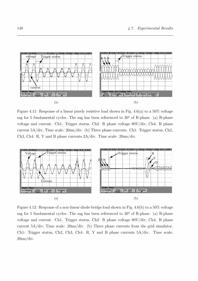
148 4.7. Experimental Results
voltage
current
Trigger status
(a)
R Y BTrigger status
(b)
Figure 4.11: Response of a linear purely resistive load shown in Fig. 4.6(a) to a 50% voltage
sag for 5 fundamental cycles. The sag has been referenced to 30o of R-phase. (a) R-phase
voltage and current. Ch1: Trigger status, Ch2: R phase voltage 80V/div, Ch4: R phase
current 5A/div, Time scale: 20ms/div. (b) Three phase currents. Ch1: Trigger status, Ch2,
Ch3, Ch4: R, Y and B phase currents 2A/div. Time scale: 20ms/div.
Trigger status
Current
Voltage
(a)
RYB
Trigger status R
Y
B
(b)
Figure 4.12: Response of a non-linear diode-bridge load shown in Fig. 4.6(b) to a 50% voltage
sag for 5 fundamental cycles. The sag has been referenced to 30o of R-phase. (a) R-phase
voltage and current. Ch1: Trigger status, Ch2: R phase voltage 80V/div, Ch4: R phase
current 5A/div, Time scale: 20ms/div. (b) Three phase currents from the grid simulator.
Ch1: Trigger status, Ch2, Ch3, Ch4: R, Y and B phase currents 5A/div. Time scale:
20ms/div.
Chapter 4. Control Performance Evaluation of Grid-Connected Inverters 149
becomes zero. The output electrolytic capacitor supplies the load current during this period.
Similarly, at the exit of the disturbance, the phase currents have a surge due to sudden
increase in the input voltage. The output electrolytic capacitor draws a peaky current
during this period due to sudden increase in the input voltage.
4.7.3.3 Current Controlled Inverter Load
In this Section experimental results of the response of the various controls of a inverter
programmed as a STATCOM is discussed. The topology of the STATCOM is shown in
Fig. 4.7. The experimental results demonstrate the usefulness of the grid simulator to test
grid-connected inverters for their control performance under grid-disturbance conditions.
Control Performance of PLL Fig. 4.13 shows the response of PLL control of a inverter
load controlled as a STATCOM as described in Section 4.6 to a change in frequency from
50Hz to 75Hz for 5 cycles of the disturbance frequency. The disturbance is referenced to
R-phase at a phase angle of 30o. The frequency change has been set to a higher value to
clearly observe the dynamics of the PLL control. As observed from Fig. 4.13(a), the PLL
control ensures that vd follows the peak of vα and vq follows zero. The control response time
is around the expected design value of 0.055s. Fig. 4.13(b) shows the cos unit vector, which
goes out of synchronism at the occurrence of the fault, locking back to the R-phase grid
voltage due to PLL control action.
Fig. 4.14 shows the response of the PLL control to a voltage sag with phase jump. The sag
disturbance is referenced to R-phase at an angle of 30o. At the beginning of the disturbance,
the phase jumps from 30o to 90o. Fig. 4.14(a), the PLL control ensures that vd follows the
peak of vα and vq follows zero and Fig. 4.14(b) shows the cos unit vector locking to the
R-phase grid voltage due to PLL control action.
Control Performance of Current Control Fig. 4.15 shows the response of the q-axis
or reactive current controller to a step change in current reference. The step change in
current reference is from zero to 8.5 A. This corresponds to a per phase current step from
zero to 4A. iq can be observed to track i∗q within half a fundamental cycle. The q-axis
current controller output has also been shown. It can be observed that the controller output
is saturated initially. This shows that the current controller’s bandwidth is limited by the

150 4.7. Experimental Results
Disturbance
duration
(a)
Disturbance duration
(b)
Figure 4.13: (a) The PLL control ensures that vd tracks the peak of vα and vq tracks zero.
Ch1, Ch2, Ch4: vd, vq, vα. Ch1, Ch2, Ch4: 200 V/div, Time scale: 20ms/div. (b) The cos
unit vector can be observed to get locked to the R-phase grid voltage due to the action of
the PLL control. Ch1, Ch2, Ch3, Ch4: sin unit vector, cos unit vector, vq and vr. Ch3: 400
V/div, Ch4: 200 V/div, Time scale: 20ms/div.
Disturbance starts here
(a)
Disturbance starts here
(b)
Figure 4.14: (a) The PLL control ensures that vd tracks the peak of vα and vq tracks zero.
Ch1, Ch3, Ch4: vd, vq, vα. Ch1, Ch3, Ch4: 200 V/div, Time scale: 10ms/div. (b) The cos
unit vector can be observed to get locked to the R-phase grid voltage due to the action of
the PLL control. Ch1, Ch2, Ch3, Ch4: sin unit vector, cos unit vector, vq and vr. Ch3, Ch4:
200 V/div, Time scale: 10ms/div.
Chapter 4. Control Performance Evaluation of Grid-Connected Inverters 151
voltage available for control. The dc bus voltage sets an upper limit on the voltage available
for control.
Control Performance of DC Bus Voltage Control Fig. 4.16 shows the response of
the dc bus voltage controller to a step change in dc bus voltage reference. The waveform
captures the voltage boost action of the STATCOM. An initial dc bus voltage exists due to
three-phase diode bridge rectification of the three-phase ac input. The voltage is boosted to
the set reference of 500V through boost action of the STATCOM. The d-axis current is also
shown in the figure. Initially the d-axis current is high and saturated. This indicates that
the STATCOM is absorbing real power to boost the dc bus voltage to 500V. Once the dc
bus voltage reaches 500V, the d-axis current becomes small as only the losses in the system
needs to be absorbed from the grid.
STATCOM Response to Sag, Swell and Phase Jump Fig. 4.17 shows the R-phase
reference voltage and the R-phase reactive current from the STATCOM under a voltage sag
of 20%, 40% and 70%. The STATCOM control can be observed to be effective under the
mentioned sag conditions.
Fig. 4.18 shows the operation of the STATCOM under a voltage swell of 15%.
Fig. 4.19 shows the operation of the STATCOM under a 20% voltage sag with a phase
jump from 30o to 90o on entering the disturbance and from 90o to 30o on exiting the dis-
turbance. The reactive current can be observed to deviate from its set reference when the
phase jump occurs but it starts tracking again within 2 cycles.
4.8 Future Scope of Work
The focus of the present work has mainly been on the development, analysis and implemen-
tation of the voltage disturbance generation algorithm. The output inverter is controlled as
a open loop voltage source. The open loop control ensures the desired output ac voltage to
be produced at the inverter output terminals. However, depending on the nature and mag-
nitude of the output three-phase currents, the ac voltage seen by the load at the output LC
filter capacitor will have deviations from the set reference. The voltage drop in the output
filter inductor leads to magnitude variations, phase angle variations and distortions in the
output capacitor voltage.
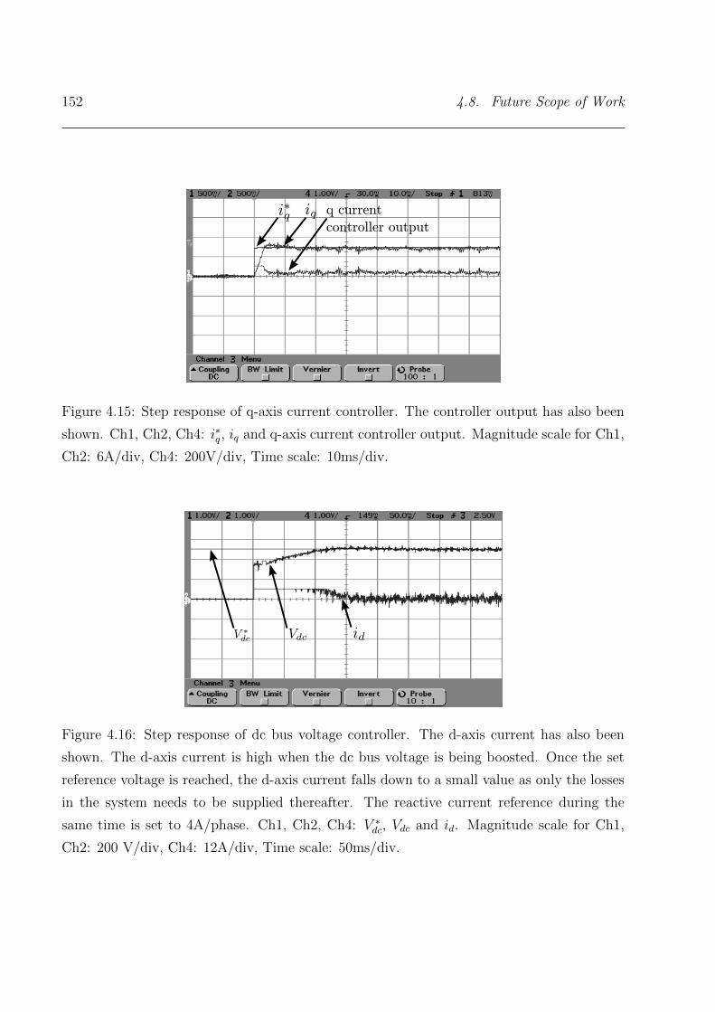
152 4.8. Future Scope of Work
q current
controller output
Figure 4.15: Step response of q-axis current controller. The controller output has also been
shown. Ch1, Ch2, Ch4: i∗q, iq and q-axis current controller output. Magnitude scale for Ch1,
Ch2: 6A/div, Ch4: 200V/div, Time scale: 10ms/div.
Figure 4.16: Step response of dc bus voltage controller. The d-axis current has also been
shown. The d-axis current is high when the dc bus voltage is being boosted. Once the set
reference voltage is reached, the d-axis current falls down to a small value as only the losses
in the system needs to be supplied thereafter. The reactive current reference during the
same time is set to 4A/phase. Ch1, Ch2, Ch4: V ∗dc, Vdc and id. Magnitude scale for Ch1,
Ch2: 200 V/div, Ch4: 12A/div, Time scale: 50ms/div.
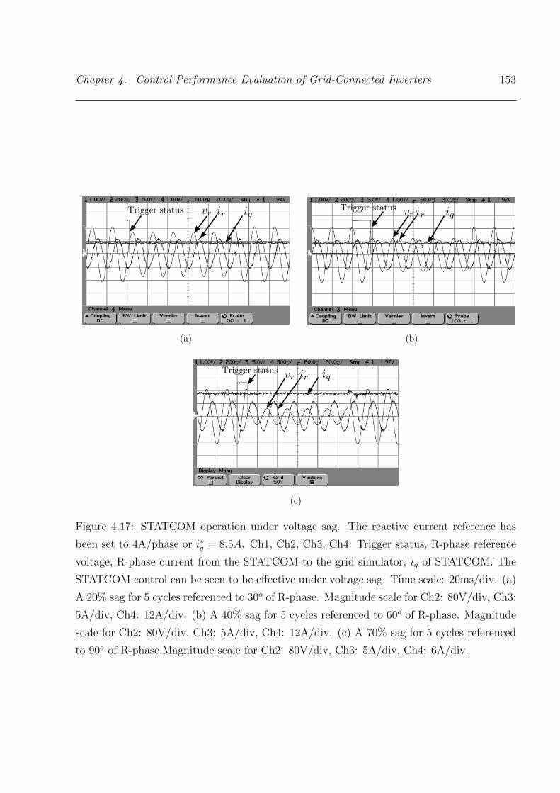
Chapter 4. Control Performance Evaluation of Grid-Connected Inverters 153
Trigger status
(a)
Trigger status
(b)
Trigger status
(c)
Figure 4.17: STATCOM operation under voltage sag. The reactive current reference has
been set to 4A/phase or i∗q = 8.5A. Ch1, Ch2, Ch3, Ch4: Trigger status, R-phase reference
voltage, R-phase current from the STATCOM to the grid simulator, iq of STATCOM. The
STATCOM control can be seen to be effective under voltage sag. Time scale: 20ms/div. (a)
A 20% sag for 5 cycles referenced to 30o of R-phase. Magnitude scale for Ch2: 80V/div, Ch3:
5A/div, Ch4: 12A/div. (b) A 40% sag for 5 cycles referenced to 60o of R-phase. Magnitude
scale for Ch2: 80V/div, Ch3: 5A/div, Ch4: 12A/div. (c) A 70% sag for 5 cycles referenced
to 90o of R-phase.Magnitude scale for Ch2: 80V/div, Ch3: 5A/div, Ch4: 6A/div.
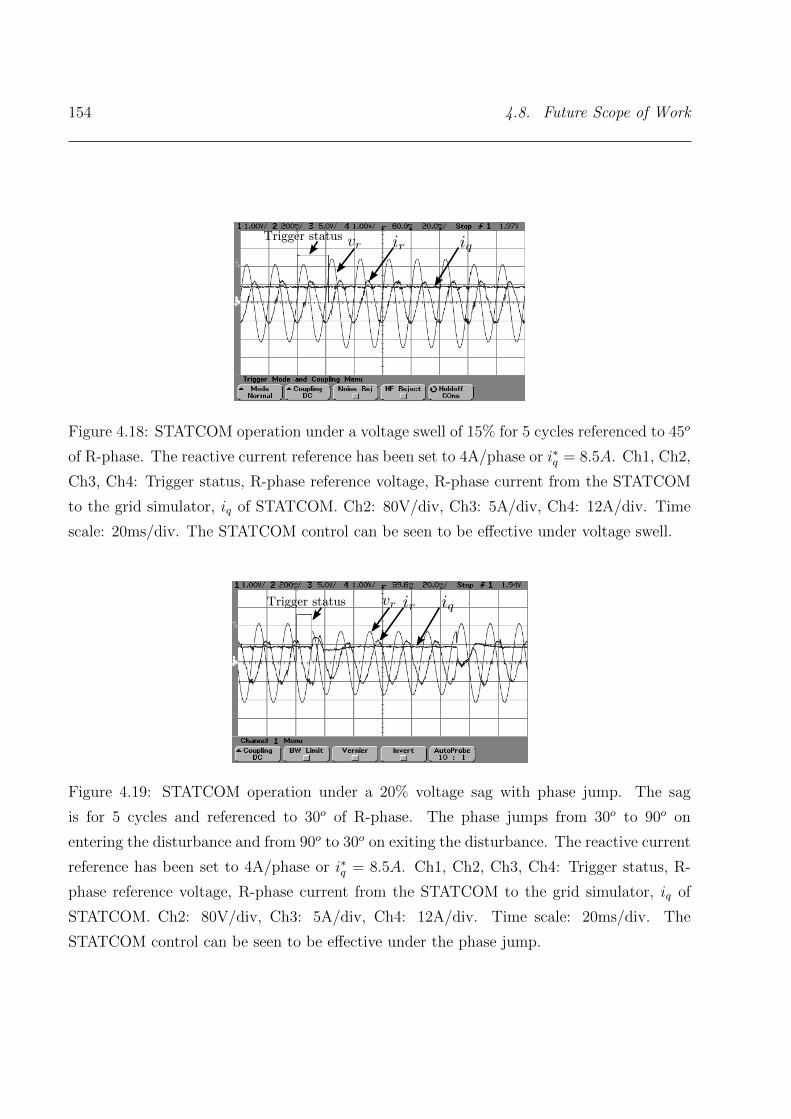
154 4.8. Future Scope of Work
Trigger status
Figure 4.18: STATCOM operation under a voltage swell of 15% for 5 cycles referenced to 45o
of R-phase. The reactive current reference has been set to 4A/phase or i∗q = 8.5A. Ch1, Ch2,
Ch3, Ch4: Trigger status, R-phase reference voltage, R-phase current from the STATCOM
to the grid simulator, iq of STATCOM. Ch2: 80V/div, Ch3: 5A/div, Ch4: 12A/div. Time
scale: 20ms/div. The STATCOM control can be seen to be effective under voltage swell.
Trigger status
Figure 4.19: STATCOM operation under a 20% voltage sag with phase jump. The sag
is for 5 cycles and referenced to 30o of R-phase. The phase jumps from 30o to 90o on
entering the disturbance and from 90o to 30o on exiting the disturbance. The reactive current
reference has been set to 4A/phase or i∗q = 8.5A. Ch1, Ch2, Ch3, Ch4: Trigger status, R-
phase reference voltage, R-phase current from the STATCOM to the grid simulator, iq of
STATCOM. Ch2: 80V/div, Ch3: 5A/div, Ch4: 12A/div. Time scale: 20ms/div. The
STATCOM control can be seen to be effective under the phase jump.

Chapter 4. Control Performance Evaluation of Grid-Connected Inverters 155
R p
hase
fee
dback
curr
ent
from
gri
d s
imula
tor
Estimated voltage drop
across the filter inductor
R phase current
from observer
PI Controller
State
Observer
Figure 4.20: Fundamental frequency current control based on state observer to improve the
output voltage of the grid simulator. The controller has been shown for the R phase. The
control is similar for the other phases. LR and RR are the output filter inductance and
associated resistance for the R phase output of the grid simulator. The estimated voltage
drop across the filter inductor is to be added to the open loop voltage reference.
To create a stiff output ac voltage across the LC filter capacitor, a feedback control using
the output filter inductor current can be implemented. A possible state observer based
current feedback scheme using Proportional-Integral (PI) controller is shown in Fig. 4.20.
The control compensates for the inductor drop at fundamental frequency by re-creating
the expected drop in the filter inductor using a state observer implemented in the digital
controller.
Alternatively, the current control shown in Fig. 4.20 can also compensate specific har-
monic voltage drops in the filter inductor by using a multi-resonant PR controller. Then the
controller transfer function would be,
Controller transfer function = Kp +∑
n=1,5,7,...
Krns
s2 + (2.π.50.n)2(92)
For further improving the stiffness of the grid simulator output voltage, an outer voltage
loop can be used in addition to the current loop. The outer voltage loop will act directly

156 4.9. Summary
on the error in the filter capacitor voltage. The accuracy of the inner current loop depends
on the exactness of the inductance and associated resistance values used in the observer.
The outer loop corrects any errors due to deviation of the filter component values from their
measured values.
4.9 Summary
A 50kVA back-to-back connected inverter is programmed as a grid simulator. A novel
voltage disturbance generation algorithm has been proposed for the grid simulator. The
proposed algorithm has been developed, analysed and implemented in digital control using
a Moore model based finite state machine. The developed grid simulator can reference
the start of the disturbance to any phase at any desired phase angle. By adjusting the
duration of the disturbance, the exit phase angle can be set with reference to any desired
phase. The magnitude, phase angle and frequency of the grid simulator output voltage
during the nominal and disturbance durations are programmable. The magnitude setting
helps create voltage sags and swells, the frequency setting helps create frequency deviations
and phase jumps can be created by setting the desired phase angle at the entry and exit of
the disturbance condition. A combination of the different settings help create a wide range
of disturbance conditions. The proposed algorithm has been validated using experimental
studies on different loads – a linear purely resistive load, a non-linear diode bridge load and
a current controlled inverter load. The developed grid simulator is useful in evaluating the
control performance of grid-connected inverters and any other equipment connected to the
grid.
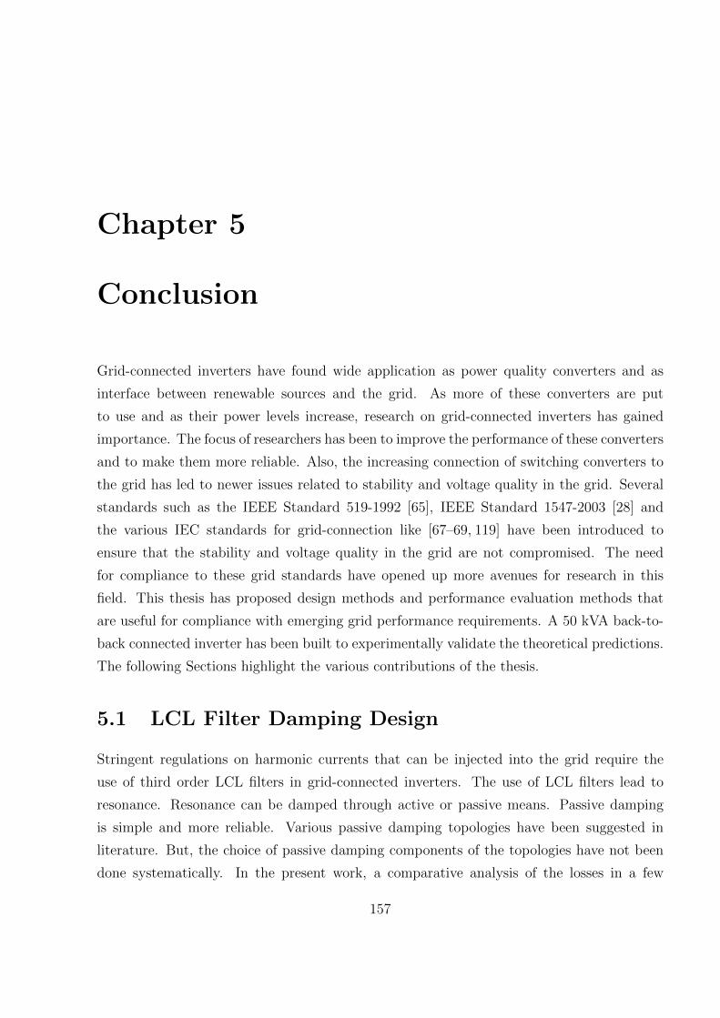
Chapter 5
Conclusion
Grid-connected inverters have found wide application as power quality converters and as
interface between renewable sources and the grid. As more of these converters are put
to use and as their power levels increase, research on grid-connected inverters has gained
importance. The focus of researchers has been to improve the performance of these converters
and to make them more reliable. Also, the increasing connection of switching converters to
the grid has led to newer issues related to stability and voltage quality in the grid. Several
standards such as the IEEE Standard 519-1992 [65], IEEE Standard 1547-2003 [28] and
the various IEC standards for grid-connection like [67–69, 119] have been introduced to
ensure that the stability and voltage quality in the grid are not compromised. The need
for compliance to these grid standards have opened up more avenues for research in this
field. This thesis has proposed design methods and performance evaluation methods that
are useful for compliance with emerging grid performance requirements. A 50 kVA back-to-
back connected inverter has been built to experimentally validate the theoretical predictions.
The following Sections highlight the various contributions of the thesis.
5.1 LCL Filter Damping Design
Stringent regulations on harmonic currents that can be injected into the grid require the
use of third order LCL filters in grid-connected inverters. The use of LCL filters lead to
resonance. Resonance can be damped through active or passive means. Passive damping
is simple and more reliable. Various passive damping topologies have been suggested in
literature. But, the choice of passive damping components of the topologies have not been
done systematically. In the present work, a comparative analysis of the losses in a few
157
158 5.2. Thermal Testing
passive topologies available in literature has been done. Based on the comparison, the SC-
RL method is chosen as a suitable passive damping topology for high power grid-connected
inverters and a component selection method for the same has been developed. The proposed
method aims at reducing the losses in the damping resistor while keeping the system well
damped. A component by component optimization and trade-off procedure is used to achieve
this. With the proposed method, the power loss in the damping resistor is in the range of
0.05% to 0.1% while the quality factor is in the range of 2.0 to 2.5. The proposed method also
ensures that the additional poles introduced by the passive damping network too are well
damped. Further, the method has been shown to be applicable for a wide range of practical
switching frequencies. The power loss and quality factor have been verified experimentally
to be within the expected range.
5.2 Thermal Testing
For better reliability, burn-in tests are performed on grid-connected inverters. Burn-in tests
are run continuously for long durations of time to allow the temperatures to stabilise. So, at
high power levels, burn-in tests consume lot of power. To ensure energy savings, regenerative
methods are usually adopted at high power levels. Also, it is not practical to have sources
and loads of high power in the testing laboratory. In this thesis, a novel method that draws
only the losses in the test configuration has been proposed and the controls required for the
same have been developed. The proposed method overcomes the shortcomings in the existing
methods. Existing methods in literature either use two inverters or require the individual
legs of the inverter to have independent cooling arrangement. The proposed method does
not have these limitations. Also, since the method circulates high currents within the test
inverter itself, it consumes less power than existing methods. A complete analysis of the
proposed method has been presented for both cases of a three-phase 3-wire configuration
and a three-phase 4-wire configuration. Further, the usefulness of the proposed method to
test the other passive components associated with the inverter like the dc bus capacitors
and output filter components has been studied. Experimental tests show a close match with
theoretical predictions.
Chapter 5. Conclusion 159
5.3 Grid Simulator
High power grid-connected inverters are required to have controls that ensure their operation
even under short time grid disturbances like voltage sag, voltage swells, frequency deviations
and phase jumps. A grid simulator is a hardware that can create a wide variety of grid
disturbances in a controlled manner in a laboratory environment to test the grid-connected
inverters for their control performance under these disturbance conditions. There are several
literature on grid simulators all of which focus mainly on the converter topology. In this
thesis, a back-to-back connected inverter is programmed as a grid simulator. The focus of
the work has been on the development of a novel disturbance voltage generation algorithm
with simple yet powerful features, for the grid simulator. The algorithm has been developed,
analysed and implemented in a digital controller using finite state machine model. The
algorithm has the flexibility to reference start of the disturbance generation to any phase at
any desired phase angle. Further, by adjusting the duration of the disturbance, the end of
the disturbance generation can be set to the desired phase angle of any phase. The control of
the start and end disturbance conditions help in studies of grid transient events with precise
details and to observe the response of the various control loops of a grid-connected inverter
to such events. The proposed algorithm also allows the precise conditions of the test to
be repeated. Further, it is possible to set the magnitude, phase and frequency of the three
phases at the start and end of the disturbance cycle. By adjusting the magnitude, voltage
sags and voltage swells can be created, by adjusting the phase angle phase jumps can be
simulated and deviations in grid frequency can be generated using the frequency parameter.
Also, a wide range of grid disturbances can be simulated through different combinations of
the mentioned parameters. The grid simulator has been experimentally tested with a linear
purely resistive load, a non-linear diode-bridge load and a current controlled STATCOM
load.
5.4 Future Scope of Work
In the proposed thermal test method, a more detailed analysis and experimental validation
can be made for the testing of dc bus capacitors and output filter components. In the
grid simulator, the front-end converter control can be modified to handle top and bottom
dc bus voltage imbalance and to mitigate second harmonic voltages in the dc bus. This

160 5.5. Summary
would help use the system to create and test unbalanced grid disturbance voltage conditions
and unbalanced loads. Further, a closed loop control for the output inverter would ensure
that the grid simulator acts as a stiff voltage source that generates the required disturbance
voltage irrespective of the load current.
5.5 Summary
Design and performance evaluation of sub-systems of grid-connected inverters has been re-
searched in this thesis. LCL filter passive damping design, a test method for thermal per-
formance evaluation and a test system for control performance evaluation are the chosen
aspects of study. Detailed study of available literature in each of the mentioned areas has
been done and significant incremental contributions has been made in each of the chosen
aspects. Firstly, a method of component selection procedure that reduces the losses in the
damping resistor while keeping the system well damped has been proposed. Then, a new
method for thermal testing of grid-connected inverters has been proposed. Finally, a test
system to study the control performance of grid-connected inverters has been developed. The
proposed methods have been verified experimentally on a back-to-back connected custom-
built inverter. The contributions have direct industrial application to improve the efficiency
and reliability of grid-connected inverters.

Appendix A
Details of Experimental Set-Up
161

162
Appendix B
Harmonic Limits: Terminology,
Definitions and Test Method
To use the current harmonic limits recommended by IEEE Standard 519–1992 [65] and IEEE
Standard 1547–2003 [28], a clear understanding of the various terminology and definitions
used by these standards is essential. In this Appendix, some terminology, definitions and test
method related to the use of the current harmonic limits recommended by the mentioned
IEEE standards is elaborated.
B.1 Point of Common Coupling (PCC)
IEEE standards define the harmonic limits at the PCC. Hence, a clear definition of PCC is
essential. Fig. B.1 shows the PCC. PCC is the point at which the local electric power system
is connected to the area electric power system [28]. In other words, it is the closest point
on the utility side of the consumer’s service where another utility consumer can potentially
be supplied [129]. To get a better idea, “Consumer 3” in Fig. B.1 can be thought of as
say, an educational institute which has some loads and a distributed source like solar energy
generation system both of which are connected to the PCC through a common transformer.
The electrical network within the educational institute can be considered as a local electric
power system. The area electric power system is the common feeder that supplies power from
the grid to a region in the city. The area electric power system would be supplying power to
different consumers in that region (Consumer 1 to Consumer 4 in this case). As shown for
“Consumer 3”, PCC need not be the point at which a distributed source is connected to the
power system through a grid-connected inverter. However, the harmonic limits are defined to
be met by the grid-connected inverter at the PCC rather than at the point of interconnection
163

164 B.2. Harmonic Measures
Area Electric Power System
Consumer 1
Consumer 2
PCC
Loads
Loca
l E
lect
ric
Pow
er S
yst
em
Consumer 3
Distributed
Source
Distributed
Source
PCC
Consumer 4
Figure B.1: Point of Common Coupling.
in the system as PCC is the point of common connectivity with other consumers. In the
figure, “Consumer 4” can be thought of as a wind farm in the neighbourhood of the institute
that is connected directly to the area electric power system. In this case the PCC happens
to be the point at which the distributed source is connected to the power system through a
grid-connected inverter.
B.2 Harmonic Measures
Harmonic content can be measured using different parameters. Each parameter has a specific
use. As can be seen in Table 2.1, the IEEE standards use the TDD to define harmonic current
limits. This Section gives the definition and use of different parameters.
Appendix B. Harmonic Limits: Terminology, Definitions and Test Method 165
B.2.1 Total Harmonic Distortion (THD)
The total harmonic distortion is the ratio of the total rms value due to all the voltage/current
harmonic components to the rms value of the fundamental component of voltage/current.
For example, the voltage THD is given by,
THD =
√√√√ ∞∑h=2
V 2h
Vfu(93)
Where,
Vh = rms value of hth harmonic component of voltage (V)
Vfu = rms value of fundamental component of voltage (V)
THD is generally not used to define the harmonic current limits at the PCC because
under lightly loaded conditions, the THD will be high even though the actual harmonics
injected is very less. This is due to the fact that the fundamental component of current will
be less under lightly loaded condition. So, if THD is used to specify the harmonic limits,
a consumer might be penalised wrongly. However, THD serves as a useful specification
for voltage harmonics at the PCC as the nominal fundamental voltage does not vary with
loading.
B.2.2 Total Demand Distortion (TDD)
The total demand distortion is the ratio of the total rms value due to all the current harmonic
components to the rms value of highest fundamental demand current (15 or 30 minute
demand). The fundamental demand current is the fundamental rms current averaged over
an interval of 15 or 30 minutes. The current TDD is given by,
TDD =
√√√√ ∞∑h=2
I2h
ID(94)
Where,
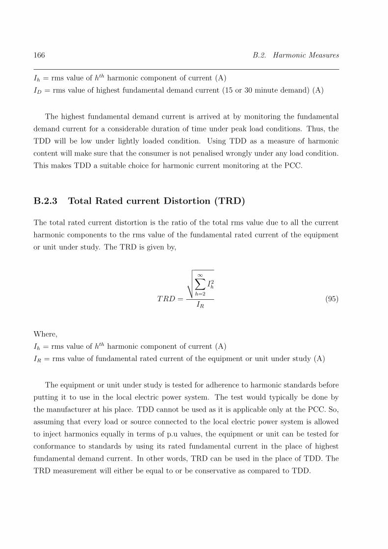
166 B.2. Harmonic Measures
Ih = rms value of hth harmonic component of current (A)
ID = rms value of highest fundamental demand current (15 or 30 minute demand) (A)
The highest fundamental demand current is arrived at by monitoring the fundamental
demand current for a considerable duration of time under peak load conditions. Thus, the
TDD will be low under lightly loaded condition. Using TDD as a measure of harmonic
content will make sure that the consumer is not penalised wrongly under any load condition.
This makes TDD a suitable choice for harmonic current monitoring at the PCC.
B.2.3 Total Rated current Distortion (TRD)
The total rated current distortion is the ratio of the total rms value due to all the current
harmonic components to the rms value of the fundamental rated current of the equipment
or unit under study. The TRD is given by,
TRD =
√√√√ ∞∑h=2
I2h
IR(95)
Where,
Ih = rms value of hth harmonic component of current (A)
IR = rms value of fundamental rated current of the equipment or unit under study (A)
The equipment or unit under study is tested for adherence to harmonic standards before
putting it to use in the local electric power system. The test would typically be done by
the manufacturer at his place. TDD cannot be used as it is applicable only at the PCC. So,
assuming that every load or source connected to the local electric power system is allowed
to inject harmonics equally in terms of p.u values, the equipment or unit can be tested for
conformance to standards by using its rated fundamental current in the place of highest
fundamental demand current. In other words, TRD can be used in the place of TDD. The
TRD measurement will either be equal to or be conservative as compared to TDD.
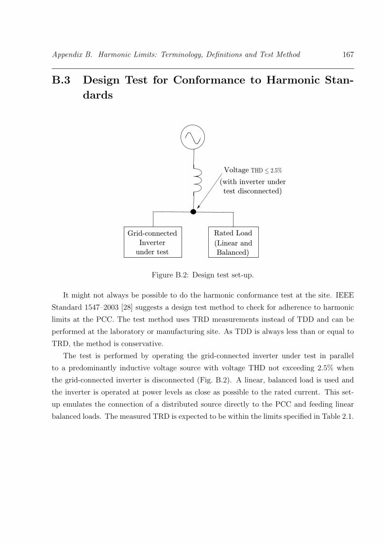
Appendix B. Harmonic Limits: Terminology, Definitions and Test Method 167
B.3 Design Test for Conformance to Harmonic Stan-
dards
Rated Load
(Linear and
Balanced)
Grid-connected
Inverter
under test
Voltage
(with inverter under
test disconnected)
Figure B.2: Design test set-up.
It might not always be possible to do the harmonic conformance test at the site. IEEE
Standard 1547–2003 [28] suggests a design test method to check for adherence to harmonic
limits at the PCC. The test method uses TRD measurements instead of TDD and can be
performed at the laboratory or manufacturing site. As TDD is always less than or equal to
TRD, the method is conservative.
The test is performed by operating the grid-connected inverter under test in parallel
to a predominantly inductive voltage source with voltage THD not exceeding 2.5% when
the grid-connected inverter is disconnected (Fig. B.2). A linear, balanced load is used and
the inverter is operated at power levels as close as possible to the rated current. This set-
up emulates the connection of a distributed source directly to the PCC and feeding linear
balanced loads. The measured TRD is expected to be within the limits specified in Table 2.1.

168 B.3. Design Test for Conformance to Harmonic Standards
Appendix C
Quality factor in the context of LCL
filter design
Quality Factor (QF) is a terminology used in resonant circuits to quantify resonance be-
haviour. Though the basic idea of resonance and the definition of QF remains the same for
grid-connected inverters with output LCL filter, the context is different from that of reso-
nant converters. In resonant converters, the power circuit operates around the resonance
frequency whereas in grid-connected inverters, the resonance occurs due to non-idealities in
the power circuit and is not desired. This Appendix tries to clarify the use of quality factor
in the context of LCL filter design.
By general definition [91],
QF = 2πTotal energy stored in the reactive components
Energy dissipated per cycle(96)
The QF is usually computed at the resonance frequency.
C.1 Quality factor in second-order series RLC circuits
Let us consider the series RLC circuit shown in Fig. C.1.
Let,
vc(t) = Vmsin(ωt) (97)
169
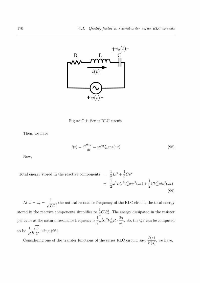
170 C.1. Quality factor in second-order series RLC circuits
---
---
Figure C.1: Series RLC circuit.
Then, we have
i(t) = Cdvcdt
= ωCVmcos(ωt) (98)
Now,
Total energy stored in the reactive components =1
2Li2 +
1
2Cv2
=1
2ω2LC2V 2
mcos2(ωt) +
1
2CV 2
msin2(ωt)
(99)
At ω = ωr =1√LC
, the natural resonance frequency of the RLC circuit, the total energy
stored in the reactive components simplifies to1
2CV 2
m. The energy dissipated in the resistor
per cycle at the natural resonance frequency is1
2ω2rC
2V 2mR ·
2π
ωr. So, the QF can be computed
to be1
R
√L
Cusing (96).
Considering one of the transfer functions of the series RLC circuit, say,I(s)
V (s), we have,

Appendix C. Quality factor in the context of LCL filter design 171
I(s)
V (s)=
sC
1 +s
1/RC+
s2
1/LC
(100)
Comparing the denominator with the standard form [91] 1 +s
(QF )ωr+s2
ω2r
, we can see
that the value of QF is the same as that derived using (96).
C.1.1 Important observations on QF
1. (96) is the general definition of QF.
2. In second order systems, the QF can be directly found by comparing the denominator
of the transfer function with the standard form 1 +s
(QF )ωr+s2
ω2r
.
3. Considering the general second order transfer function1
1 +s
(QF )ωr+s2
ω2r
, QF is the
magnitude of the asymptotic bode plot at the resonance frequency [91]. The actual
peak of the bode plot appears slightly away from the resonance frequency. However,
without loss of much accuracy, the magnitude at the resonance frequency is always
considered as it can readily be obtained from the transfer function.
4. In second order systems, considering the other standard formω2r
ω2r + 2ζωrs+ s2
, the
damping factor ζ can be observed to be1
2(QF ). Thus, a low QF translates into better
damping.
5. From the expression QF =1
R
√L
C, for a given L and C, a low QF or equivalently a
better damping indicates more losses as the resistance has to be increased to achieve
better damping.
172 C.2. Quality factor in higher order systems
C.2 Quality factor in higher order systems
The quality factor in higher order systems is complicated by the presence of more than one
resonance. The multiple resonance frequencies might be well seperated or might appear close
by. Due to this, the magnitude of the bode plot at the natural resonance frequencies are not
a good approximation for the QF. The magnitude of the peak of the bode plot would be a
good indicator to characterize the resonance in this case. The peak of the bode plot appears
at ωd, the damped resonance frequency. So, the QF can be computed as,
QF =
∣∣∣∣VC(jω)
Vi(jω)
∣∣∣∣at ω = ωd∣∣∣∣VC(jω)
Vi(jω)
∣∣∣∣ω → 0
(101)
The above equation is valid for second order systems also. It would be more accurate
than the QF expression1
R
√L
C.
C.2.1 Application in LCL filter design
In this thesis, (101) has been used for LCL filter damping design as the circuit is of higher
order. A low QF is desirable as the design aims at damping the resonance. This is in
contrast to resonant converters where a high QF is desirable as the circuit is intended to be
operated around resonance and a low QF will lead to higher losses. In LCL filters, resonance
phenomenon is due to non-idealities present in the inverter and associated circuitry while
the converter itself is intended to be operated at the fundamental frequency which is not
same as the resonance frequency. Through damping, the resonance component of current is
kept low. A higher damping does require use of a higher value of resistance. However, the
low QF ensures that the resonance component of current to be very low and thus the losses
due to that component also is low and can usually be neglected as compared to the losses in
the damping resistor due to the fundamental frequency and switching ripple components of
current.

Appendix D
Quality Factor and Power Loss
Expressions
Quality factor (QF) and damping resistor power loss are two parameters that can be used
to assess a passive damping scheme. While the QF is a measure of level of damping, the
power loss in the damping resistor indicates the trade-off in efficiency due to the addition of
the passive damping network. This Appendix lists the state space models and expressions
for quality factor and power loss in case of R and SC-R passive damping schemes shown in
Fig. D.1.
D.1 State Space Model
The state space models for R and SC-R damped LCL filters can be developed using the state
variables (ii, ig, vcap) and (ii, ig, vc, vd) respectively. Fig. D.1 shows the mentioned state
variables. iRdis the output variable for both the cases as the power loss in the damping
resistor is the quantity of interest in either case. The state space equations appear below:
D.1.1 R Passive Damping
The state space equations are,
x(t) = Ax(t) + Bu(t)
y(t) = Cx(t) + Du(t)(102)
173

174 D.1. State Space Model
+
_
+
_
+
_
_
+
C
L1 L2
Rd
vcap
vC
ig
vi vg
ii
iRd
(a)
+++
+
_ _ _
_
Rd
Cd
C1
L1 L2
ii
vd
ig
iRd
vC vgvi
(b)
Figure D.1: Passive damping schemes. (a) Purely Resistive (R) damping scheme. (b) Split-
Capacitor Resistive (SC-R) damping scheme.
Where,
A=
−Rd
L1
Rd
L1
− 1
L1
Rd
L2
−Rd
L2
1
L2
1
C− 1
C0
; B=
1
L1
0
0 − 1
L2
0 0
; x=
ii
ig
vcap
;
u=
[vi
vg
]; C= [1 − 1 0]; D= [0 0]; y= iRd
;
D.1.2 SC-R Passive Damping
The state space equations are,

Appendix D. Quality Factor and Power Loss Expressions 175
x(t) = Ax(t) + Bu(t)
y(t) = Cx(t) + Du(t)(103)
Where,
A=
0 0 − 1
L1
0
0 01
L2
0
1
C1
− 1
C1
− 1
C1Rd
1
C1Rd
0 01
CdRd
− 1
CdRd
; B=
1
L1
0
0 − 1
L2
0 0
0 0
; x=
ii
ig
vC
vd
;
u=
[vi
vg
]; C=
[0 0
1
Rd
− 1
Rd
]; D= [0 0]; y= iRd
;
D.2 Quality Factor
Using Fig. D.1 and the steps listed in Section 2.4.2.2, the transfer functionVC(s)
Vi(s)and the
simplified approximate QF expressions for R and SC-R passive damping schemes can be
derived and is given below:
D.2.1 R Passive Damping
Using simple circuit principles,
VC(s)
Vi(s)=
L2 s+Rd C L2 s2
(L1 + L2)s+RdC(L1 + L2)s2 + CL1L2s3(104)
With L1 = L2 = L/2, the QF can be derived to be,

176 D.3. Power Loss
QF =
√1 +
L
4R2dC
(105)
D.2.2 SC-R Passive Damping
Using simple circuit principles,
VC(s)
Vi(s)=
L2 s+Rd Cd L2 s2
(L1 + L2)s+RdCd(L1 + L2)s2 + L1L2(C1 + Cd)s3 +RdL1L2C1Cds4(106)
With L1 = L2 = L/2 and C1 = Cd = C/2, the QF can be derived to be,
QF = 2×
√1 +
L
CR2d
(107)
D.3 Power Loss
The power loss in the passive damping network primarily consists of two components -
the fundamental frequency component, Pfu, and the switching ripple component, Pri. The
fundamental frequency loss component can be computed using simple circuit principles as-
suming vC = 1p.u. in Fig. D.1 as explained in Section 2.4.2.3 while the power loss due to the
switching ripple component can be computed using state space analysis outlined in the same
Section. The closed form expressions for the fundamental frequency loss component in R
and SC-R passive damping schemes are given below. The switching ripple loss component is
computed numerically using the state space models in Section D.1 and hence does not have
closed form expressions.
D.3.1 R Passive Damping
Using simple circuit principles and taking vC to be 1 p.u.,
Pfu(p.u.) =C2Rd
1 + C2R2d
(108)

Appendix D. Quality Factor and Power Loss Expressions 177
D.3.2 SC-R Passive Damping
Using simple circuit principles, with C1 = Cd = C/2 and taking vC to be 1 p.u.,
Pfu(p.u.) =C2dRd
1 + C2dR
2d
(109)

178 D.3. Power Loss

Appendix E
Computation of Semiconductor Power
Losses in Inverter
The power loss in the semiconductor devices of an inverter has the following components:
1. Conduction Loss
a. IGBT conduction loss
b. Diode conduction loss
2. Switching Loss
a. IGBT turn-on loss
b. IGBT turn-off loss
c. Diode reverse recovery loss
3. Module Terminal Loss
The equations used in this thesis to compute the various power loss components are based
on [101]. This Appendix gives the list of formulas used along with some pointers to derive
the same.
Conventions Used: Fig. E.1(a) describes the voltage polarity and current direction con-
ventions used in the power loss equations described in this Appendix. Fig. E.1(b) describes
the power factor angle ψ at the output terminal of the inverter leg. It also shows the con-
duction periods of the IGBTs and diodes shown in Fig. E.1(a).
179

180 E.1. Conduction Loss
_
__
_ __
(a) (b)
Figure E.1: Conventions used for power loss computations. (a) One leg of the inverter
showing conventions used in power loss computations. (b) Current and voltage waveform
at the output of the inverter describing angle ψ and conduction periods of top and bottom
IGBTs and diodes.
E.1 Conduction Loss
E.1.1 IGBT Conduction Loss
The average conduction loss (PS cond) in top IGBT of one leg of the inverter can be computed
as,
PS cond =1
2π
∫ 2π
0
pS(t) d(ωt) (110)
where, pS(t) represents the instantaneous conduction loss in the top IGBT and is given
by,
pS(t) =
[VCE0 + rCE · i(t)] · i(t) ·D(t), i(t) ≥ 0
0, i(t) < 0(111)
where, VCE0, rCE are datasheet parameters of the IGBT, i(t) is the instantaneous current
at the output terminal as shown in Fig. E.1(a) and D(t) is the instantaneous duty ratio of
the top IGBT.

Appendix E. Computation of Semiconductor Power Losses in Inverter 181
Assuming sinusoidal voltages and currents at the output of the inverter terminal as shown
in Fig. E.1 with a peak current of Im, modulation index of ‘m’ under sine-triangle modulation
scheme and power factor angle ψ, the closed form expression for average conduction loss in
top IGBT, PS cond can be derived to be,
PS cond =1
2
[VCE0
πIm +
rCE4I2m
]+m · cosψ
[VCE0
8Im +
rCE3π
I2m
](112)
The conduction loss expression for the bottom IGBT can be derived in a similar manner.
The only difference is the conduction period. The bottom IGBT conducts only for i(t) ≤ 0.
The final expression given by (112) is the same for the bottom IGBT also.
E.1.2 Diode Conduction Loss
The average conduction loss (PD cond) in bottom diode of one leg of the inverter can be
computed as,
PD cond =1
2π
∫ 2π
0
pD(t) d(ωt) (113)
where, pD(t) represents the instantaneous conduction loss in the bottom diode and is
given by,
pD(t) =
[VF0 + rF · i(t)] · i(t) ·D′(t), i(t) ≥ 0
0, i(t) < 0(114)
where, VF0, rF are datasheet parameters of the diode, i(t) is the instantaneous current
at the output terminal as shown in Fig. E.1(a) and D′(t) is the instantaneous duty ratio of
the bottom diode.
Assuming sinusoidal voltages and currents at the output of the inverter terminal as shown
in Fig. E.1 with a peak current of Im, modulation index of ‘m’ under sine-triangle modulation
scheme and power factor angle ψ, the closed form expression for average conduction loss in
bottom diode, PS cond can be derived to be,
PD cond =1
2
[VF0
πIm +
rF4I2m
]−m · cosψ
[VF0
8Im +
rF3πI2m
](115)
The conduction loss expression for the top diode can be derived in a similar manner. The
only difference is the conduction period. The top diode conducts only for i(t) ≤ 0. The final
expression given by (115) is the same for the top diode also.
182 E.2. Switching Loss
E.1.3 IGBT and Diode Conduction Losses in CSVPWM
The IGBT and Diode conduction losses can still be computed using (110), (111), (113) and
(114). However, the instantaneous duty ratios D(t) and D′(t) are different from that of the
sine PWM scheme. The instantaneous duty ratio in any PWM scheme is directly related to
the modulating reference waveform. Hence, the difference in the instantaneous duty ratios
of the two schemes arise due to the common mode. To get simplified closed form expres-
sions, the common mode can be approximated by a triangular waveform and the triangular
waveform’s fundamental frequency component alone can be used in the computation of the
instantaneous duty ratio without significant loss of accuracy [104]. This adds the following
additional terms to (112) and (115) [104],
For IGBT Conduction Loss: − 2
15π3· I2m · rCE ·m · cos(3ψ)
For Diode Conduction Loss: +2
15π3· I2m · rF ·m · cos(3ψ)
E.2 Switching Loss
E.2.1 IGBT Turn-on and Turn-off Losses
The average switching loss (PS sw) in any IGBT of the inverter can be computed as,
PS sw =1
2π
∫ 2π
0
pS,sw(t) d(ωt) (116)
where, pS,sw(t) represents the instantaneous switching loss in the IGBT.
Assuming linear variation of Eon and Eoff w.r.t current, the average switching loss in
one IGBT can be approximated to be,
PS sw = fsw · [Eon +Eoff ] ·√
2
π· irateditest
·(
VdcVdc,test
)KV,IGBT
· (1 +TCEsw(Tj,IGBT −Tref )) (117)
where,

Appendix E. Computation of Semiconductor Power Losses in Inverter 183
fsw : operating switching frequency
irated : rated current
itest : current at which the datasheet parameters have been taken
KV,IGBT : exponent for voltage dependency of switching loss ∼ 1.3 . . . 1.4
TCEsw : temperature co-efficient of the switching loss ∼ 0.003 per oC
Tj,IGBT : operating junction temperature of the IGBT
Tref : reference junction temperature at which the datasheet parameters have been taken
The other parameters are datasheet parameters as mentioned in Table 3.5.
E.2.2 Diode Reverse Recovery Loss
The average reverse recovery loss (PD rr) in any diode of the inverter can be computed as,
PD rr =1
2π
∫ 2π
0
pD,rr(t) d(ωt) (118)
where, pD,rr(t) represents the instantaneous reverse recovery loss in the diode.
The average reverse recovery loss in one diode can be approximated to be,
PD rr = fsw ·Err ·
(√2
π· irateditest
)KI,diode
·(
VdcVdc,test
)KV,diode
· (1 +TCErr(Tj,diode−Tref )) (119)
where,
fsw : operating switching frequency
irated : rated current
itest : current at which the datasheet parameters have been taken
KI,diode : exponent for current dependency of reverse recovery loss ∼ 0.6
KV,diode : exponent for voltage dependency of reverse recovery loss ∼ 0.6
TCErr : temperature co-efficient of the reverse recovery loss ∼ 0.006 per oC
Tj,diode : operating junction temperature of the diode
Tref : reference junction temperature at which the datasheet parameters have been taken
The other parameters are datasheet parameters as mentioned in Table 3.5.

184 E.3. Module Terminal Loss
E.3 Module Terminal Loss
The datasheet parameter RCC′+EE′ specifies the lead resistance of the terminals on a per
module basis. One module has one leg of the inverter. The power loss per leg or module due
to the terminal lead resistance is given by,
PMod term = I2rms ·RCC′+EE′ (120)

References
[1] P. Sensarma, K. Padiyar, and V. Ramanarayanan, “Analysis and performance evalua-
tion of a distribution STATCOM for compensating voltage fluctuations,” IEEE Trans-
actions on Power Delivery, vol. 16, no. 2, pp. 259–264, 2001.
[2] Arun Karuppaswamy B, “Synchronous reference frame strategy based STATCOM for
reactive and harmonic current compensation,” M.Tech Thesis, National Institute of
Technology, Calicut., June 2007.
[3] A. Unnikrishnan, A. Joseph, and T. Subhash Joshi, “Three level STATCOM based
power quality solution for a 4 MW induction furnace,” in Proceedings of the In-
ternational Conference on Power Electronics, Drives and Energy Systems, 2006.
PEDES’06., pp. 1–5, IEEE, 2006.
[4] J. G. Nielsen, F. Blaabjerg, and N. Mohan, “Control strategies for dynamic voltage re-
storer compensating voltage sags with phase jump,” in Proceedings of the Sixteenth An-
nual IEEE Applied Power Electronics Conference and Exposition, 2001. APEC 2001.,
vol. 2, pp. 1267–1273, IEEE, 2001.
[5] V. Surendran and V. Srikanth, “Performance improvement of dynamic voltage restorer
using Proportional-Resonant controller,” in Proceedings of the Power and Energy Sys-
tems Conference: Towards Sustainable Energy, 2014, pp. 1–5, IEEE, 2014.
[6] H. Fujita and H. Akagi, “The Unified Power Quality Conditioner: The integration
of series and shunt-active filters,” IEEE Transactions on Power Electronics, vol. 13,
no. 2, pp. 315–322, 1998.
[7] Y. Chen, X. Zha, J. Wang, H. Liu, J. Sun, and H. Tang, “Unified Power Quality
Conditioner (UPQC): The theory, modeling and application,” in Proceedings of the
185

186 References
International Conference on Power System Technology, 2000. PowerCon 2000., vol. 3,
pp. 1329–1333, IEEE, 2000.
[8] J. M. Carrasco, L. G. Franquelo, J. T. Bialasiewicz, E. Galvan, R. P. Guisado, M. A.
Prats, J. I. Leon, and N. Moreno-Alfonso, “Power-electronic systems for the grid in-
tegration of renewable energy sources: A survey,” IEEE Transactions on Industrial
Electronics, vol. 53, no. 4, pp. 1002–1016, 2006.
[9] J. S. Prasad, T. Bhavsar, R. Ghosh, and G. Narayanan, “Vector control of three-phase
AC/DC front-end converter,” Sadhana, vol. 33, no. 5, pp. 591–613, 2008.
[10] A. L. Julian, T. Lipo, and G. Oriti, “Elimination of common mode voltage in three
phase sinusoidal power converters,” in Proceedings of 27th Annual IEEE Power Elec-
tronics Specialists Conference, 1996. PESC’96,, vol. 2, pp. 1968–1972, IEEE, 1996.
[11] J. M. Carrasco, L. G. Franquelo, J. T. Bialasiewicz, E. Galvan, R. P. Guisado, M. A.
Prats, J. I. Leon, and N. Moreno-Alfonso, “Power-electronic systems for the grid in-
tegration of renewable energy sources: A survey,” IEEE Transactions on Industrial
Electronics, vol. 53, no. 4, pp. 1002–1016, 2006.
[12] S. B. Kjaer, J. K. Pedersen, and F. Blaabjerg, “A review of single-phase grid-connected
inverters for photovoltaic modules,” IEEE Transactions on Industry Applications,
vol. 41, no. 5, pp. 1292–1306, 2005.
[13] J. Rodriguez, J.-S. Lai, and F. Z. Peng, “Multilevel inverters: a survey of topologies,
controls, and applications,” IEEE Transactions on Industrial Electronics, vol. 49, no. 4,
pp. 724–738, 2002.
[14] Y. Xue, L. Chang, S. B. Kjaer, J. Bordonau, and T. Shimizu, “Topologies of single-
phase inverters for small distributed power generators: an overview,” IEEE Transac-
tions on Power Electronics, vol. 19, no. 5, pp. 1305–1314, 2004.
[15] M. Calais, V. G. Agelidis, and M. Meinhardt, “Multilevel converters for single-phase
grid connected photovoltaic systems: an overview,” Solar Energy, vol. 66, no. 5,
pp. 325–335, 1999.

References 187
[16] J. Kolar and S. Round, “Analytical calculation of the RMS current stress on the DC-
link capacitor of voltage-PWM converter systems,” In IEE Proceedings of Electric
Power Applications, vol. 153, no. 4, pp. 535–543, 2006.
[17] N. Celanovic and D. Boroyevich, “A comprehensive study of neutral-point voltage bal-
ancing problem in three-level neutral-point-clamped voltage source PWM inverters,”
IEEE Transactions on Power Electronics, vol. 15, no. 2, pp. 242–249, 2000.
[18] V. Sankaran, F. Rees, and C. Avant, “Electrolytic capacitor life testing and prediction,”
in Conference Record of the IEEE Industry Applications Conference, 1997., vol. 2,
pp. 1058–1065, IEEE, 1997.
[19] H. Beukes, J. Enslin, and R. Spee, “Busbar design considerations for high power IGBT
converters,” in Proceedings of the 28th Annual IEEE Power Electronics Specialists
Conference, 1997. PESC’97, vol. 2, pp. 847–853, IEEE, 1997.
[20] M. C. Caponet, F. Profumo, R. W. De Doncker, and A. Tenconi, “Low stray induc-
tance bus bar design and construction for good EMC performance in power electronic
circuits,” IEEE Transactions on Power Electronics, vol. 17, no. 2, pp. 225–231, 2002.
[21] L. Popova, T. Musikka, R. Juntunen, M. Lohtander, P. Silventoinen, O. Pyrhonen, and
J. Pyrhonen, “Modelling of low inductive busbars for medium voltage three-level NPC
inverter,” in Proceedings of Power Electronics and Machines in Wind Applications
(PEMWA), 2012, pp. 1–7, IEEE, 2012.
[22] M. Ando, K. Wada, K. Takao, T. Kanai, S. Nishizawa, and H. Ohashi, “Design and
analysis of a bus bar structure for a medium voltage inverter,” in Proceedings of the
2011-14th European Conference on Power Electronics and Applications (EPE 2011),
pp. 1–10, IEEE, 2011.
[23] X. Zhang, H. Zhang, R.-W. Yu, and G.-J. Tan, “Planar bus bar optimum design in
high-power converters based on FEM analysis,” in 2nd IEEE International Symposium
on Power Electronics for Distributed Generation Systems (PEDG), 2010, pp. 167–170,
IEEE, 2010.
[24] J. Wang, B. Yang, J. Zhao, Y. Deng, X. He, and X. Zhixin, “Development of a com-
pact 750kVA three-phase NPC three-level universal inverter module with specifically

188 References
designed busbar,” in Proceedings of Twenty-Fifth Annual IEEE Applied Power Elec-
tronics Conference and Exposition (APEC), 2010, pp. 1266–1271, IEEE, 2010.
[25] F. Blaabjerg, “Snubbers in PWM-VSI-inverter,” in Proceedings of 22nd Annual IEEE
Power Electronics Specialists Conference, 1991, PESC’91., pp. 104–111, IEEE, 1991.
[26] X. He, S. J. Finney, B. W. Williams, and Z.-M. Qian, “Novel passive lossless turn-
on snubber for voltage source inverters,” IEEE Transactions on Power Electronics,
vol. 12, no. 1, pp. 173–179, 1997.
[27] F. Blaabjerg and J. K. Pedersen, “An optimum drive and clamp circuit design with
controlled switching for a snubberless PWM-VSI-IGBT inverter leg,” in Proceedings of
23rd Annual IEEE Power Electronics Specialists Conference, 1992. PESC’92., pp. 289–
297, IEEE, 1992.
[28] “IEEE standard for interconnecting distributed resources with electric power systems,”
IEEE Std 1547-2003, 2003.
[29] A. Rockhill, M. Liserre, R. Teodorescu, and P. Rodriguez, “Grid-filter design for a
multi-megawatt medium-voltage voltage-source inverter,” IEEE Transactions on In-
dustrial Electronics, vol. 58, no. 4, pp. 1205–1217, 2011.
[30] M. Prodanovic and T. C. Green, “Control and filter design of three-phase inverters for
high power quality grid connection,” IEEE Transactions on Power Electronics, vol. 18,
no. 1, pp. 373–380, 2003.
[31] K. Ahmed, S. Finney, and B. Williams, “Passive filter design for three-phase inverter
interfacing in distributed generation,” in Proceedings of Compatibility in Power Elec-
tronics, 2007. CPE ’07, pp. 1 –9, June 2007.
[32] F. Liu, X. Zha, Y. Zhou, and S. Duan, “Design and research on parameter of LCL filter
in three-phase grid-connected inverter,” in IEEE 6th International Power Electronics
and Motion Control Conference, 2009. IPEMC’09., pp. 2174–2177, IEEE, 2009.
[33] M. Liserre, F. Blaabjerg, and S. Hansen, “Design and control of an LCL-filter-based
three-phase active rectifier,” IEEE Transactions on Industry Applications, vol. 41,
no. 5, pp. 1281–1291, 2005.
References 189
[34] T. Wang, Z. Ye, G. Sinha, and X. Yuan, “Output filter design for a grid-interconnected
three-phase inverter,” in IEEE 34th Annual Power Electronics Specialist Conference,
2003. PESC ’03. 2003, vol. 2, pp. 779 – 784, June 2003.
[35] G. Zeng, T. Rasmussen, L. Ma, and R. Teodorescu, “Design and control of LCL-filter
with active damping for active power filter,” in Proceedings of IEEE International
Symposium on Industrial Electronics (ISIE, 2010), pp. 2557 –2562, July 2010.
[36] J. Dannehl, F. Fuchs, S. Hansen, and P. Th andgersen, “Investigation of active damp-
ing approaches for PI-based current control of grid-connected pulse width modulation
converters with LCL filters,” IEEE Transactions on Industrial Applications, vol. 46,
pp. 1509 –1517, July-August 2010.
[37] W. Zhao and G. Chen, “Comparison of active and passive damping methods for appli-
cation in high power active power filter with LCL-filter,” in Proceedings of SUPERGEN
’09., pp. 1 –6, April 2009.
[38] S. Ogasawara, H. Ayano, and H. Akagi, “An active circuit for cancellation of common-
mode voltage generated by a PWM inverter,” in Proceedings of 28th Annual IEEE
Power Electronics Specialists Conference, 1997. PESC’97,, vol. 2, pp. 1547–1553,
IEEE, 1997.
[39] Y.-C. Son and S.-K. Sul, “A new active common-mode EMI filter for PWM inverter,”
IEEE Transactions on Power Electronics, vol. 18, no. 6, pp. 1309–1314, 2003.
[40] H. Akagi, H. Hasegawa, and T. Doumoto, “Design and performance of a passive EMI
filter for use with a voltage-source PWM inverter having sinusoidal output voltage and
zero common-mode voltage,” in Proceedings of IEEE 33rd Annual Power Electronics
Specialists Conference, 2002. PESC 02., vol. 3, pp. 1543–1550, IEEE, 2002.
[41] H. Zhu, J.-S. Lai, A. R. Hefner, Y. Tang, and C. Chen, “Modeling-based examination
of conducted EMI emissions from hard and soft-switching PWM inverters,” IEEE
Transactions on Industry Applications, vol. 37, no. 5, pp. 1383–1393, 2001.
[42] S. Azuma, M. Kimata, M. Seto, X. Jiang, H. Lu, D. Xu, and L. Huang, “Research
on the power loss and junction temperature of power semiconductor devices for in-
190 References
verter,” in Proceedings of the IEEE International Vehicle Electronics Conference,
1999.(IVEC’99), pp. 183–187, IEEE, 1999.
[43] T.-J. Kim, D.-W. Kang, Y.-H. Lee, and D.-S. Hyun, “The analysis of conduction and
switching losses in multi-level inverter system,” in Proceedings of IEEE 32nd Annual
Power Electronics Specialists Conference, 2001. PESC., vol. 3, pp. 1363–1368, IEEE,
2001.
[44] J. He, V. Mehrotra, and M. C. Shaw, “Thermal design and measurements of IGBT
power modules: transient and steady state,” in Conference Record of the 1999 IEEE
Industry Applications Conference, 1999., vol. 2, pp. 1440–1444, IEEE, 1999.
[45] F. Blaabjerg and J. K. Pedersen, “Optimized design of a complete three-phase PWM-
VS inverter,” IEEE Transactions on Power Electronics, vol. 12, no. 3, pp. 567–577,
1997.
[46] M. A. Boost and P. D. Ziogas, “State-of-the-art carrier PWM techniques: A critical
evaluation,” IEEE Transactions on Industry Applications, vol. 24, no. 2, pp. 271–280,
1988.
[47] A. M. Trzynadlowski, “An overview of modern PWM techniques for three-phase,
voltage-controlled, voltage-source inverters,” in Proceedings of the IEEE International
Symposium on Industrial Electronics, 1996. ISIE’96,, vol. 1, pp. 25–39, IEEE, 1996.
[48] G. Narayanan, H. K. Krishnamurthy, D. Zhao, and R. Ayyanar, “Advanced bus-
clamping PWM techniques based on space vector approach,” IEEE Transactions on
Power Electronics, vol. 21, no. 4, pp. 974–984, 2006.
[49] G. Carrara, S. Gardella, M. Marchesoni, R. Salutari, and G. Sciutto, “A new multilevel
PWM method: A theoretical analysis,” IEEE Transactions on Power Electronics,
vol. 7, no. 3, pp. 497–505, 1992.
[50] F. Wang, “Sine-triangle versus space-vector modulation for three-level PWM voltage-
source inverters,” IEEE Transactions on Industry Applications, vol. 38, no. 2, pp. 500–
506, 2002.
References 191
[51] J. W. Kimball and M. Zawodniok, “Reducing common-mode voltage in three-phase
sine-triangle PWM with interleaved carriers,” IEEE Transactions on Power Electron-
ics, vol. 26, no. 8, pp. 2229–2236, 2011.
[52] S. Chung, “Phase-locked loop for grid-connected three-phase power conversion sys-
tems,” in IEE Proceedings on Electric Power Applications, vol. 147, pp. 213–219, IET,
2000.
[53] M. Ciobotaru, R. Teodorescu, and V. G. Agelidis, “Offset rejection for PLL based
synchronization in grid-connected converters,” in Proceedings of Twenty-Third An-
nual IEEE Applied Power Electronics Conference and Exposition, 2008. APEC 2008.,
pp. 1611–1617, IEEE, 2008.
[54] A. Nicastri and A. Nagliero, “Comparison and evaluation of the PLL techniques for
the design of the grid-connected inverter systems,” in IEEE International Symposium
on Industrial Electronics (ISIE), 2010, pp. 3865–3870, IEEE, 2010.
[55] E. Twining and D. G. Holmes, “Grid current regulation of a three-phase voltage source
inverter with an LCL input filter,” IEEE Transactions on Power Electronics, vol. 18,
no. 3, pp. 888–895, 2003.
[56] F. A. Magueed and J. Svensson, “Control of VSC connected to the grid through LCL-
filter to achieve balanced currents,” in Proceedings of Fourtieth IAS Industry Applica-
tions Conference, 2005., vol. 1, pp. 572–578, IEEE, 2005.
[57] J. Dannehl, C. Wessels, and F. W. Fuchs, “Limitations of voltage-oriented PI current
control of grid-connected PWM rectifiers with filters,” IEEE Transactions on Industrial
Electronics, vol. 56, no. 2, pp. 380–388, 2009.
[58] S. Mariethoz and M. Morari, “Explicit model-predictive control of a PWM inverter
with an LCL filter,” IEEE Transactions on Industrial Electronics, vol. 56, no. 2,
pp. 389–399, 2009.
[59] F. Liu, Y. Zhou, S. Duan, J. Yin, B. Liu, and F. Liu, “Parameter design of a two-
current-loop controller used in a grid-connected inverter system with LCL filter,” IEEE
Transactions on Industrial Electronics, vol. 56, no. 11, pp. 4483–4491, 2009.
192 References
[60] G. Shen, X. Zhu, J. Zhang, and D. Xu, “A new feedback method for PR current
control of LCL-filter-based grid-connected inverter,” IEEE Transactions on Industrial
Electronics, vol. 57, no. 6, pp. 2033–2041, 2010.
[61] Dong Choon Lee, G Myoung Lee, Ki Do Lee, “DC-bus voltage control of three-phase
AC/DC PWM converters using feedback linearization,” IEEE Transactions on Indus-
try Applications, vol. 36, no. 3, pp. 826–833, 2000.
[62] F. Z. Peng, “A generalized multilevel inverter topology with self voltage balancing,”
IEEE Transactions on Industry Applications, vol. 37, no. 2, pp. 611–618, 2001.
[63] Z. Pan, F. Z. Peng, K. A. Corzine, V. R. Stefanovic, J. M. Leuthen, and S. Gataric,
“Voltage balancing control of diode-clamped multilevel rectifier/inverter systems,”
IEEE Transactions on Industry Applications, vol. 41, no. 6, pp. 1698–1706, 2005.
[64] H. L. Liu, N. S. Choi, and G. H. Cho, “DSP based space vector PWM for three-level
inverter with DC-link voltage balancing,” in Proceedings of International Conference on
Industrial Electronics, Control and Instrumentation, 1991. Proceedings. IECON’91.,
1991, pp. 197–203, IEEE, 1991.
[65] “IEEE recommended practices and requirements for harmonic control in electrical
power systems,” IEEE Std 519-1992, 1993.
[66] IEEE Industry Applications Society, “IEEE draft recommended practice for voltage
sag and interruption ride-through testing for end use electrical equipment less than
1,000 volts,” IEEE.
[67] IEC Standards Committee, SC-77A, “Electromagnetic compatibility (EMC) - part 3-
2: Limits - limits for harmonic current emissions (equipment input current 16 a per
phase),” IEC, 2014.
[68] IEC Standards Committee, SC-77A, “Electromagnetic compatibility (EMC) - part 4-
11: Testing and measurement techniques - voltage dips, short interruptions and voltage
variations immunity tests,” IEC, 2004.
[69] IEC Standards Committee, SC-77A, “Electromagnetic compatibility (EMC) - part 4-
34: Testing and measurement techniques - voltage dips, short interruptions and voltage
References 193
variations immunity tests for equipment with mains current more than 16 a per phase,”
IEC, 2009.
[70] IEC Standards Committee, SC-77A, “Electromagnetic compatibility (EMC) - part 4-
13: Testing and measurement techniques - harmonics and interharmonics including
mains signalling at a.c. power port, low frequency immunity tests,” IEC, 2009.
[71] IEC Standards Committee, SC-88, “Wind turbines - part 21: Measurement and as-
sessment of power quality characteristics of grid connected wind turbines,” IEC, 2008.
[72] IEC Standards Committee, SC-82, “Utility-interconnected photovoltaic inverters - test
procedure of islanding prevention measures,” IEC, 2014.
[73] C. Ayres and I. Barbi, “Power recycler for DC power supplies burn-in test: design
and experimentation,” in Conference Proceedings of Annual Applied Power Electronics
Conference and Exposition, 1996. APEC ’96, vol. 1, pp. 72–78 vol.1, 1996.
[74] C. Ayres and I. Barbi, “A family of converters for UPS production burn-in energy
recovery,” IEEE Transactions on Power Electronics, vol. 12, no. 4, pp. 615–622, 1997.
[75] C.-E. Lin, M.-T. Tsai, W.-I. Tsai, and C.-L. Huang, “Consumption power feedback
unit for power electronics burn-in test,” IEEE Transactions on Industrial Electronics,
vol. 44, no. 2, pp. 157–166, 1997.
[76] Y. Tsuruta and A. Kawamura, “Back to back system for the development and testing
of high power DC-DC converter,” in Proceedings of 34th Annual Conference of IEEE
Industrial Electronics, IECON 2008, pp. 572–577, 2008.
[77] C. Roncero-Clemente, M. Milanes-Montero, V. Minambres-Marcos, and E. Romero-
Cadaval, “Three-phase regenerative electronic load to test shunt power conditioners,”
in Proceedings of 7th International Conference-Workshop on Compatibility and Power
Electronics (CPE), 2011, pp. 178–183, 2011.
[78] C. L. Chu and J. F. Chen, “Self-load bank for UPS testing by circulating current
method,” In IEE Proceedings of Electric Power Applications, vol. 141, no. 4, pp. 191–
196, 1994.
194 References
[79] C. Oates, “Accelerated life testing of a traction inverter,” Power Engineering Journal,
vol. 13, no. 5, pp. 263–271, 1999.
[80] M. Tsai, “Comparative investigation of the energy recycler for power electronics burn-
in test,” In IEE Proceedings of Electric Power Applications, vol. 147, no. 3, pp. 192–198,
2000.
[81] F. Forest, J. J. Huselstein, S. Faucher, M. Elghazouani, P. Ladoux, T. Meynard,
F. Richardeau, and C. Turpin, “Use of opposition method in the test of high-power
electronic converters,” IEEE Transactions on Industrial Electronics, vol. 53, no. 2,
pp. 530–541, 2006.
[82] C. Prasad and G. Narayanan, “Proportional resonant controller based circulating
power setup for thermal testing of multilevel inverter,” in Proceedings of 7th IEEE
International Conference on Industrial and Information Systems (ICIIS), 2012, pp. 1–
6, 2012.
[83] R. Lohde and F. Fuchs, “Laboratory type PWM grid emulator for generating dis-
turbed voltages for testing grid connected devices,” in Proceedings of 13th European
Conference on Power Electronics and Applications, 2009. EPE ’09., pp. 1–9, Sept
2009.
[84] J. Eloy-Garcia, J. Vasquez, and J. Guerrero, “Grid simulator for power quality assess-
ment of micro-grids,” IET Power Electronics, vol. 6, pp. 700–709, April 2013.
[85] M. Cespedes, T. Qi, and J. Sun, “Development of a grid simulator,” in Proceedings of
the 13th Workshop on Control and Modeling for Power Electronics (COMPEL), 2012,
pp. 1–8, June 2012.
[86] N. Kim, S.-Y. Kim, H.-G. Lee, C. Hwang, G.-H. Kim, H.-R. Seo, M. Park, and I.-K.
Yu, “Design of a grid-simulator for a transient analysis of grid-connected renewable
energy system,” in Proceedings of International Conference on Electrical Machines and
Systems (ICEMS), 2010, pp. 633–637, Oct 2010.
[87] F. Li, X. Wang, Z. Chen, and X. Zhang, “A laboratory grid simulator based on three-
phase four-leg inverter: Design and implementation,” in Proceedings of the Interna-

References 195
tional Conference on Electrical Machines and Systems (ICEMS), 2011, pp. 1–5, Aug
2011.
[88] S. Hu, J. Li, and H. Xu, “Comparison of voltage sag generators for wind power system,”
in Proceedings of Power and Energy Engineering Conference, 2009, APPEEC 2009.,
pp. 1–4, March 2009.
[89] B. C. Parikshith, “Integrated approach to filter design for grid connected power con-
verters,” Master’s thesis, Indian Institute of Science, Bangalore, July 2009.
[90] C. T. Chen, Linear System Theory and Design. Oxford University Press, 3rd ed., 1999.
[91] R. Erickson and D. Maksimovic, Fundamentals of Power Electronics. Kluwer Academic
Publishers, 2nd ed., 2001.
[92] Y. Han, C. Chung, H. Yoo, J. Kim, and S. Kim, “A test facility for large scale inverter
valve and pole using resonant circuit,” in Proceedings of 7th Internatonal Conference
on Power Electronics, 2007. ICPE ’07, pp. 548–553, 2007.
[93] J. Chen, C. L. Chu, and C. Huang, “A study on the test of UPS by energy feedback
method,” in Proceedings of IEEE International Sympoisum on Circuits and Systems,
1991, pp. 3015–3018 vol.5, 1991.
[94] S. Gupta, V. Rangaswamy, and R. Ruth, “Load bank elimination for UPS testing,” in
Conference Record of the 1990 IEEE Industry Applications Society Annual Meeting,
1990, pp. 1040–1043 vol.2, 1990.
[95] M. Giesselmann, B. Crittenden, and J. Fonseca, “Design and test of a high power
inverter for a ground based radar system for theater missile defense,” in Digest of
Technical Papers of 11th IEEE International Pulsed Power Conference, 1997, vol. 2,
pp. 1542–1547 vol.2, 1997.
[96] G. Kim, H. Lee, S. Oh, C. Lee, and S. Park, “Study on real-time load simulator
for testing propulsion inverter test,” in Proceedings of International Joint Conference
SICE-ICASE, 2006, pp. 3858–3863, 2006.
[97] D. G. Holmes and T. A. Lipo, Pulse Width Modulation for Power Converters - Prin-
ciples and Practice. IEEE Press, 2003.

196 References
[98] Y. Sato, T. Ishizuka, K. Nezu, and T. Kataoka, “A new control strategy for voltage-
type PWM rectifiers to realize zero steady-state control error in input current,” IEEE
Transactions on Industry Applications, vol. 34, no. 3, pp. 480–486, 1998.
[99] D. Zmood and D. Holmes, “Stationary frame current regulation of PWM inverters
with zero steady-state error,” IEEE Transactions on Power Electronics, vol. 18, no. 3,
pp. 814–822, 2003.
[100] A. Yepes, F. Freijedo, J. Doval-Gandoy, O. Lopez, J. Malvar, and P. Fernandez-
Comesaa, “Effects of discretization methods on the performance of resonant con-
trollers,” IEEE Transactions on Power Electronics, vol. 25, no. 7, pp. 1692–1712,
2010.
[101] A. Wintrich, U. Nicolai, T. Reimann, and W. Tursky, “Semikron application manual
- power semiconductors.” http://www.semikron.com/. Accessed: May, 2013.
[102] “SKM150GB12T4G IGBT datasheet.” http://www.semikron.com/. Accessed:
March, 2009.
[103] F. Casanellas, “Losses in PWM inverters using IGBTs,” IEE Proceedings - Electric
Power Applications, vol. 141, no. 5, pp. 235–239, 1994.
[104] J. Kolar, F. Zach, and F. Casanellas, “Losses in PWM inverters using IGBTs,” IEE
Proceedings - Electric Power Applications, vol. 142, no. 4, pp. 285–288, 1995.
[105] “HCV electrolytic capacitors datasheet.” http://www.alconelectronics.com/. Ac-
cessed: March, 2009.
[106] M. Gasperi, “A method for predicting the expected life of bus capacitors,” in Confer-
ence Record of the 1997 IEEE Industry Applications Conference, 1997, vol. 2, pp. 1042–
1047 vol.2, 1997.
[107] Epcos, “Epcos general technical information on capacitors for power electronics.”
http://www.epcos.com/. Accessed: May, 2013.
[108] A.E.Fitzgerald, C. Kingsley, and S. D. Umans, Electric Machinery. Mc-Graw Hill,
6th ed., 2002.
References 197
[109] Y. Chung, G. H. Kwon, T. B. Park, and G. Y. Lim, “Voltage sag and swell generator
with thyristor controlled reactor,” in Proceedings of International Conference on Power
System Technology, 2002. Proceedings. PowerCon 2002., vol. 3, pp. 1933–1937 vol.3,
2002.
[110] E. Collins and R. L. Morgan, “A three-phase sag generator for testing industrial equip-
ment,” IEEE Transactions on Power Delivery, vol. 11, pp. 526–532, Jan 1996.
[111] Y. Chung, G. H. Kwon, T. B. Park, H. Kim, and J. I. Moon, “Voltage sag, swell and
flicker generator with series injected inverter,” in Proceedings of Power Engineering
Society General Meeting, 2005., pp. 1308–1313 Vol. 2, June 2005.
[112] F. Wagner, R. Schmuki, T. Wagner, and P. Wolstenholme, Modeling software with
finite state machines: a practical approach. CRC Press, 2006.
[113] ABB, “ACS 6000 Grid Simulator.” http://www05.abb.com/global/scot/scot216.
nsf/veritydisplay/19178deab3265e81c1257abf002e9e4a/$file/ACS%206000%
20grid%20simulator_lowres.pdf. Accessed: July, 2014.
[114] Ametek, “MX CTS Series Grid Simulator.” http://www.calinst.com/products/
MXCTS/MXCTS_Overview.htm. Accessed: July, 2014.
[115] Chroma, “61800 Grid Simulator.” http://www.chromausa.com/blog/ac-sources/
new-high-power-regenerative-grid-simulators-test-on-grid-products/. Ac-
cessed: July, 2014.
[116] Heiden, “TC ACS Series Grid Simulator.” http://www.heidenpower.com/en/home/
67-products/net-simulator/325-grid-simulator-systems.html. Accessed: July,
2014.
[117] Federal Energy Regulatory Commission, “Interconnection standards for wind energy,”
FERC, 2005.
[118] North American Electric Reliability Corporation, “Generator frequency and voltage
protective relay settings,” NERC, 2013.
[119] IEC Standards Committee, SC-77A, “Electromagnetic compatibility (EMC) - part 3-
3: Limits - limitation of voltage changes, voltage fluctuations and flicker in public

198 References
low-voltage supply systems, for equipment with rated current 16 a per phase and not
subject to conditional connection,” IEC, 2013.
[120] IEC Standards Committee, SC-77A, “Electromagnetic compatibility (EMC) - part 3-
11: Limits - limitation of voltage changes, voltage fluctuations and flicker in public low-
voltage supply systems - equipment with rated current 75 a and subject to conditional
connection,” IEC, 2000.
[121] IEC Standards Committee, SC-77A, “Electromagnetic compatibility (EMC) - part 3-
12: Limits - limits for harmonic currents produced by equipment connected to public
low-voltage systems with input current ¿16 a and 75 a per phase,” IEC, 2011.
[122] IEC Standards Committee, SC-77A, “Electromagnetic compatibility (EMC) - part
4-14: Testing and measurement techniques - voltage fluctuation immunity test for
equipment with input current not exceeding 16 a per phase,” IEC, 2009.
[123] IEC Standards Committee, SC-77A, “Electromagnetic compatibility (EMC) - part 4-
17: Testing and measurement techniques - ripple on d.c. input power port immunity
test,” IEC, 2009.
[124] IEC Standards Committee, SC-77A, “Electromagnetic compatibility (EMC) - part 4-
28: Testing and measurement techniques - variation of power frequency, immunity test
for equipment with input current not exceeding 16 a per phase,” IEC, 2009.
[125] IEC Standards Committee, SC-77A, “Electromagnetic compatibility (EMC) - part 4-
29: Testing and measurement techniques - voltage dips, short interruptions and voltage
variations on d.c. input power port immunity tests,” IEC, 2000.
[126] IEC Standards Committee, SC-77A, “Electromagnetic compatibility (EMC) - part
3-15: Limits - assessment of low frequency electromagnetic immunity and emission
requirements for dispersed generation systems in lv network,” IEC, 2011.
[127] V. Kaura and V. Blasko, “Operation of a phase locked loop system under distorted
utility conditions,” in Proceedings of Eleventh Annual Applied Power Electronics Con-
ference and Exposition, 1996. APEC’96., vol. 2, pp. 703–708, IEEE, 1996.

References 199
[128] M. Ciobotaru, R. Teodorescu, and F. Blaabjerg, “A new single-phase PLL structure
based on second order generalized integrator,” in Proceedings of 37th IEEE Power
Electronics Specialists Conference, 2006. PESC’06., pp. 1–6, IEEE, 2006.
[129] T. Blooming and D. Carnovale, “Application of IEEE Std 519-1992 harmonic limits,”
in Conference Record of Annual Pulp and Paper Industry Technical Conference, 2006,
pp. 1–9, June 2006.