Embed Size (px)
Citation preview

HIGH-PERFORMANCE DIGITAL FILTER IN FPGA
SITI SUHAILA MOHD YUSOF
UNIVERSITI TEKNOLOGI MALAYSIA
ii
HIGH-PERFORMANCE DIGITAL FILTER IN FPGA
SITI SUHAILA MOHD YUSOF
A project report submitted in partial fulfilment of the
requirements for the award of the degree of
Master of Engineering (Electrical – Microelectronics and Computer System)
Faculty of Electrical Engineering
Universiti Teknologi Malaysia
JUNE 2013

iv
Specially dedicated to my beloved family, lecturers and friends
for the guidance, encouragement and inspiration throughout my journey of education

v
ACKNOWLEDGEMENT
First of all, I would like to put on record my indebtedness to my project
supervisor and mentor, Prof. Dr. Mohamed Khalil bins Hj Mohd Hani for his
guidance and teachings throughout the progress of this project. He has not only
provided me with many opportunities to learn more and gain experiences in this field
of study, but also taught me the fundamentals of a good technical documentation.
This report would not have been successful without his advice.
I would also like to express my gratitude to all authors and experts whose
research results and findings that I have been referring to that provides crucial
knowledge and clarifications in completing this project.
Special thanks to Intel Microelectronics (M) Sdn. Bhd. for funding my
studies. I would like to thank my manager Ng, Chin Leng as well as my colleagues
who had provided me with help and support throughout the duration of my studies. I
would also want to extend my gratitude to my classmates, especially Lim Ee Ric,
Baba, Beenal and Kam Kok Horng for all the knowledge sharing.
Last but not least, I would like to thank my direct family for giving me the
support and encouragement throughout my studies.
vi
ABSTRACT
Digital filtering algorithms are most commonly implemented using general
purpose digital signal processing chips for audio applications, or special purpose
digital filtering chips and application- specific integrated circuits (ASICs) for higher
rates. Based on the study digital filter which is Infinite Impulse Response (IIR) filter,
the filter is generally used in the lower sample rates, that is less than 200 kHz (2009)
[2]. These filters are used over a wide range of sample rates and are well supported in
terms of tools, software, and IP cores. In this research, a high performance and area
optimized infinite impulse response (IIR) filter realization in field programmable
gate arrays (FPGAs) is proposed. The advantages of the FPGA approach to digital
filter implementation include higher sampling rates than are available from
traditional DSP chips, lower costs than an ASIC for moderate volume applications,
and more flexibility than the alternate approaches. Since many current FPGA
architectures are in-system programmable, the configuration of the device may be
changed to implement different functionality if required. The main goal of this
project is to mapping data flow graphs (DFGs) from the BiQuad architecture direct
form II of Infinite Impulse Response filtering algorithms into application specific
structure is considered. This filter realizes BiQuad Methods was structured with the
high throughput, high clock frequency (Fmax), low Critical Path Delay (CPD), and
low Latency (L). Optimization method is proposed which provides designing
pipelined structures, concurrent, minimal resource utilization and minimized
sensitivity to truncation errors. A digital filter which is compatible with simulation
tool (software) Verilog HDL Quartus II and Matlab presented in preliminary results
chapter 5.
Keywords – Digital IIR filter, FPGA, Verilog HDL, MATLAB, and Quartus II.

vii
ABSTRAK
Digital penapisan algoritma adalah yang paling biasa dilaksanakan dengan
menggunakan tujuan umum digital cip pemprosesan isyarat untuk aplikasi audio,
atau tujuan digital cip penapisan khas dan litar bersepadu khusus aplikasi (ASIC)
untuk kadar yang lebih tinggi. Berdasarkan kajian penapis digital yang mana Impulse
Response Infinite (IIR) biasanya digunakan dalam kadar sampel yang lebih rendah,
dan kurang daripada 200 kHz (2009) [2]. Penapis ini digunakan dalam pelbagai
kadar sampel dan disokong dari segi alat, perisian, dan teras IP. Dalam kajian ini,
infinite impulse response (IIR) dioptimumkan menggunakan field programmable
gate arrays (FPGAs) dicadangkan. Kelebihan pendekatan FPGA untuk pelaksanaan
penapis digital termasuk kadar sampel yang lebih tinggi daripada yang boleh didapati
dari tradisional cip DSP, kos yang lebih rendah daripada satu ASIC untuk aplikasi
jumlah yang sederhana, dan lebih fleksibel daripada pendekatan alternatif. FPGA
memang telah banyak digunakan dalam sistem diprogramkan, konfigurasi peranti ini
boleh diubah untuk melaksanakan fungsi yang berbeza jika diperlukan. Matlamat
utama projek ini adalah untuk pemetaan graf aliran data (DFGs) daripada BiQuad
bentuk langsung II. Menyedari Kaedah BiQuad telah distrukturkan dengan
pemprosesan yang tinggi, dan frekuensi yang tinggi (Fmax), tempoh masa yang
rendah (CPD), dan Latency yang rendah (L). Kaedah pengoptimuman adalah
dicadangkan yang menyediakan bentuk struktur saluran maklumat, serentak,
penggunaan sumber yang minimum dan sensitiviti dikurangkan kepada kesilapan
pemangkasan. Satu penapis digital yang serasi dengan simulasi alat (perisian)
Verilog HDL Quartus II dan Matlab dibentangkan dalam keputusan awal bab 5.
Kata Kunci – Penapis IIR , FPGA, Verilog HDL, MATLAB, dan Quartus II.
viii
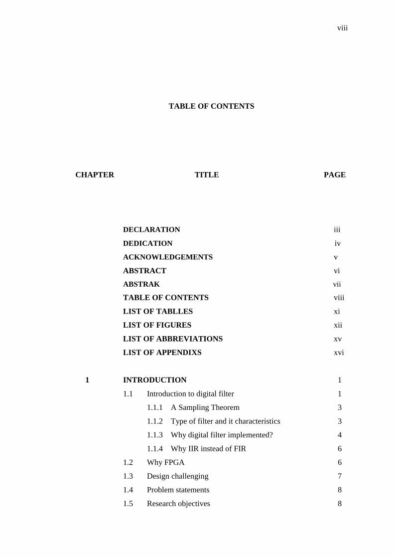
TABLE OF CONTENTS
CHAPTER TITLE PAGE
DECLARATION iii
DEDICATION iv
ACKNOWLEDGEMENTS v
ABSTRACT vi
ABSTRAK vii
TABLE OF CONTENTS viii
LIST OF TABLLES xi
LIST OF FIGURES xii
LIST OF ABBREVIATIONS xv
LIST OF APPENDIXS xvi
1 INTRODUCTION 1
1.1 Introduction to digital filter 1
1.1.1 A Sampling Theorem 3
1.1.2 Type of filter and it characteristics 3
1.1.3 Why digital filter implemented? 4
1.1.4 Why IIR instead of FIR 6
1.2 Why FPGA 6
1.3 Design challenging 7
1.4 Problem statements 8
1.5 Research objectives 8

ix
1.6 Research Motivation and Objectives 9
1.7 Design Outcome and Expected Contribution 10
1.8 Scope of work 11
2 LITERATURE RESEARCH 12
2.1 Principle of Filter Operations 12
2.2 Quantization and Finite Word-length Effects 15
2.3 Design for FPGA implementation 20
2.4 BiQuad architecture 22
2.5 Digital filter using BiQuad approaches. 24
2.5.1 Single Cycles (Concurrent design) 25
2.5.2 Multi Cycles with Resource Constrains 26
2.5.3 Pipelined design 27
3 METHODOLOGY AND IMPLEMENTATION 29
3.1 General approach: Bit true model realization 29
3.1.1 How to design filter in Matlab 30
3.1.2 Coefficient Quantization and Intermediate
word length 31
3.2 A study of FPGA Implementations 34
3.2.1 A study on how to Results output from FPGA 35
3.2.2 Design Debugging Using the Signal-Tap II Logic
Analyzer 35
3.2.3 Design target and optimization 36
3.3 IIR Band Stop filter modeled in Matlab and specification 37
4 DESIGN AND MODELING 40
4.1 High level BiQuad of IIR filter 40
4.1.1 Synchronous Dataflow Graph (SDFG) of IIR Filter 41
4.1.2 Algorithm for BiQuad IIR Filter 42
4.2 Analysis on Cyclone II EP2C35F672C6 family
characteristics unit library 43
4.3 Single Cycle (concurrent) 44
4.3.1 DFG and ASM chart for Single Cycle (concurrent) 44
x
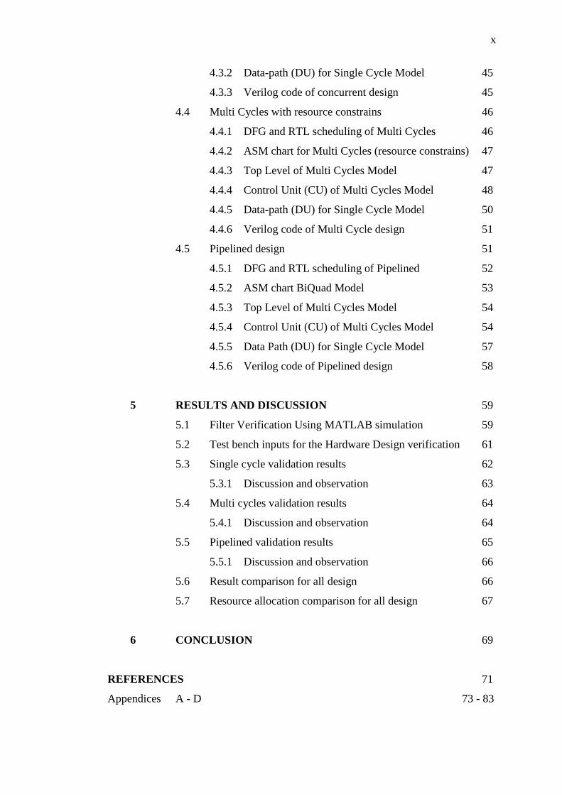
4.3.2 Data-path (DU) for Single Cycle Model 45
4.3.3 Verilog code of concurrent design 45
4.4 Multi Cycles with resource constrains 46
4.4.1 DFG and RTL scheduling of Multi Cycles 46
4.4.2 ASM chart for Multi Cycles (resource constrains) 47
4.4.3 Top Level of Multi Cycles Model 47
4.4.4 Control Unit (CU) of Multi Cycles Model 48
4.4.5 Data-path (DU) for Single Cycle Model 50
4.4.6 Verilog code of Multi Cycle design 51
4.5 Pipelined design 51
4.5.1 DFG and RTL scheduling of Pipelined 52
4.5.2 ASM chart BiQuad Model 53
4.5.3 Top Level of Multi Cycles Model 54
4.5.4 Control Unit (CU) of Multi Cycles Model 54
4.5.5 Data Path (DU) for Single Cycle Model 57
4.5.6 Verilog code of Pipelined design 58
5 RESULTS AND DISCUSSION 59
5.1 Filter Verification Using MATLAB simulation 59
5.2 Test bench inputs for the Hardware Design verification 61
5.3 Single cycle validation results 62
5.3.1 Discussion and observation 63
5.4 Multi cycles validation results 64
5.4.1 Discussion and observation 64
5.5 Pipelined validation results 65
5.5.1 Discussion and observation 66
5.6 Result comparison for all design 66
5.7 Resource allocation comparison for all design 67
6 CONCLUSION 69
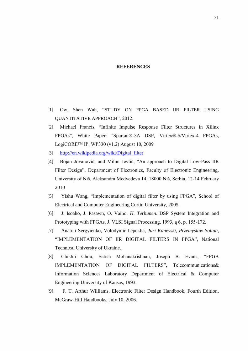
REFERENCES 71
Appendices A - D 73 - 83
xi
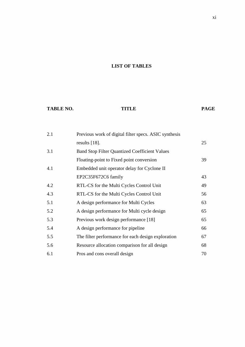
LIST OF TABLES
TABLE NO. TITLE PAGE
2.1 Previous work of digital filter specs. ASIC synthesis
results [18]. 25
3.1 Band Stop Filter Quantized Coefficient Values
Floating-point to Fixed point conversion 39
4.1 Embedded unit operator delay for Cyclone II
EP2C35F672C6 family 43
4.2 RTL-CS for the Multi Cycles Control Unit 49
4.3 RTL-CS for the Multi Cycles Control Unit 56
5.1 A design performance for Multi Cycles 63
5.2 A design performance for Multi cycle design 65
5.3 Previous work design performance [18] 65
5.4 A design performance for pipeline 66
5.5 The filter performance for each design exploration 67
5.6 Resource allocation comparison for all design 68
6.1 Pros and cons overall design 70

xii
LIST OF FIGURES
FIGURE NO. TITLE PAGE
1.1 Illustration of digital filter band Stop 2
1.2 Digital Filter System 3
1.3 Internal structures of generic FPGA 7
2.1 Time and Frequency Domain Response of a Band pass Filter 13
2.2 Template from FDATOOL of Band stop filter 14
2.3 An ADC based digital conversation system 16
2.4 A saturating arithmetic operational behavior 17
2.5 Truncation vs. rounding in fixed-point representation 17
2.6 Arithmetic Error in a fixed-point MAC unit 18
2.7 Frequency of a FIR with coefficients determined using SA 19
2.8 (a) SFG & (b) DFG of a DSP recursion y(n) = ay(n − 1) + x(n) 21
2.9 Example of (a) before (b) after pipelining 21
2.10 BiQuad direct form II architecture 23
2.11 Cascaded BiQuad structure 24
2.12 Single Cycle implementation of a BiQuad system 26
2.13 Multi Cycles implementation of a BiQuad system 26
2.14 Scheduling diagram from paper “Hardware Implementation
Analysis for Digital Filters” 2006 [18]. From the
approach the delay of multiplier is ~10ns 27
2.15 Transposed Direct II form second order IIR (BiQuad).
Dashed lines are critical loops. 28
2.16 Alternative realization of a pipelined BiQuad critical timing [19] 28
3.1 A fixed-point filter design procedure compatible in FPGA 30
xiii
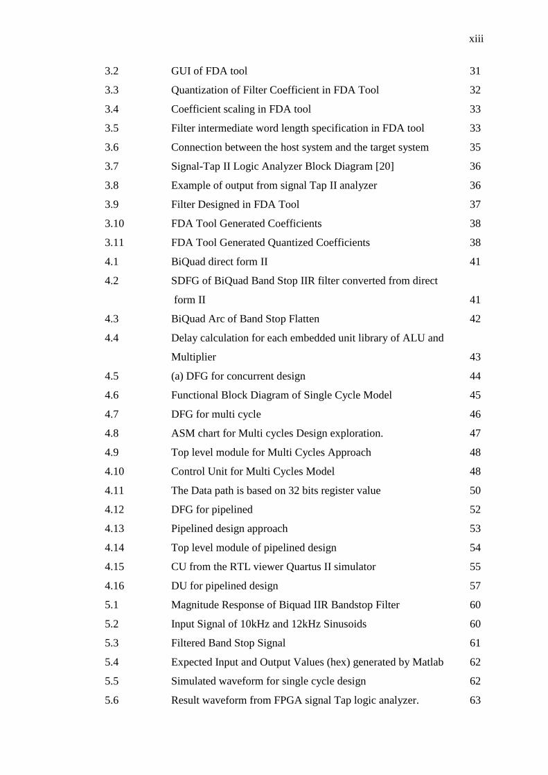
3.2 GUI of FDA tool 31
3.3 Quantization of Filter Coefficient in FDA Tool 32
3.4 Coefficient scaling in FDA tool 33
3.5 Filter intermediate word length specification in FDA tool 33
3.6 Connection between the host system and the target system 35
3.7 Signal-Tap II Logic Analyzer Block Diagram [20] 36
3.8 Example of output from signal Tap II analyzer 36
3.9 Filter Designed in FDA Tool 37
3.10 FDA Tool Generated Coefficients 38
3.11 FDA Tool Generated Quantized Coefficients 38
4.1 BiQuad direct form II 41
4.2 SDFG of BiQuad Band Stop IIR filter converted from direct
form II 41
4.3 BiQuad Arc of Band Stop Flatten 42
4.4 Delay calculation for each embedded unit library of ALU and
Multiplier 43
4.5 (a) DFG for concurrent design 44
4.6 Functional Block Diagram of Single Cycle Model 45
4.7 DFG for multi cycle 46
4.8 ASM chart for Multi cycles Design exploration. 47
4.9 Top level module for Multi Cycles Approach 48
4.10 Control Unit for Multi Cycles Model 48
4.11 The Data path is based on 32 bits register value 50
4.12 DFG for pipelined 52
4.13 Pipelined design approach 53
4.14 Top level module of pipelined design 54
4.15 CU from the RTL viewer Quartus II simulator 55
4.16 DU for pipelined design 57
5.1 Magnitude Response of Biquad IIR Bandstop Filter 60
5.2 Input Signal of 10kHz and 12kHz Sinusoids 60
5.3 Filtered Band Stop Signal 61
5.4 Expected Input and Output Values (hex) generated by Matlab 62
5.5 Simulated waveform for single cycle design 62
5.6 Result waveform from FPGA signal Tap logic analyzer. 63
xiv
5.7 Simulated waveform for Multi Cycle design 64
5.8 Simulated waveform for pipelined design 66
xv
LIST OF ABBREVIATIONS
ADC - Analog-to-Digital Converter
ASIC - Application-specific Integrated Circuit
CU - Control Unit
DU - Datapath Unit
DAC - Digital-to-Analog Converter
DSP - Digital Signal Processing
FIR - Finite Impulse Response
FPGA - Field-programmable Gate Array
FT - Fourier Transform
GUI - Graphical User Interface
HDL - Hardware Descriptive Language
IIR - Infinite Impulse Response
LTI - Linear Time Invariant
LSB - Least Significant Bit
LUT - Look-up Table
MAC - Multiplication-Accumulation Unit
MSB - Most Significant Bit
RAM - Random Access Memory
RTL - Register-transfer Level
SA - Simulated Annealing
SNR - Signal-to-noise Ratio
VLSI - Very-Large-Scale Integration
xvi
LIST OF APPENDICES
APPENDIX TITLE PAGE
A Verilog program for Single Cycle (concurrent) 73
filter design
B Verilog program for Multi Cycles 75
(with resource constrains) filter design
C Verilog program for pipelined 78
(with resource constrains) filter design
D Matlab IIR filter Code 81

1
CHAPTER 1
1 INTRODUCTION
Digital filter has been a subject of interest for Digital Signal Processing
(DSP) systems due to its enormous technology impacts and limitless applications.
With the advancement of silicon scaling and digital architecture, Field Programmable
Grid Array (FPGA) is also no longer a stranger in the electronics field. In this
chapter, an overview of digital filters and FPGA is presented. This is followed by the
motivation, objectives and the scope of work that would be achieved in the project.
1.1 Introduction to digital filter
In electronics, computer science and mathematics, a digital filter is a system
that performs mathematical operations on a sampled, discrete-time signal to reduce
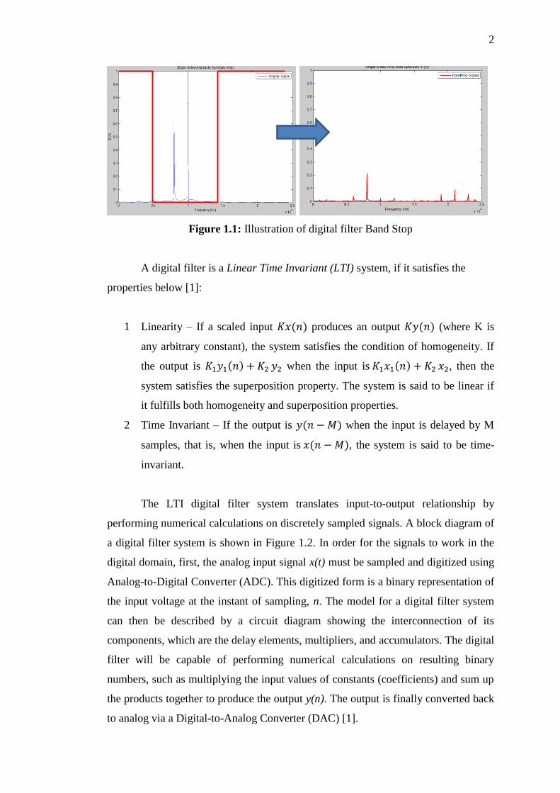
or enhance certain aspects of that signal [3]. Refer figure 1.1 illustration on how the
filter works. The figure illustrated on the Band Stop filters which to eliminate the
certain frequency which not allowed passing to the system. The red line is
determined by filter characteristics which are called cutoff frequency. Basically for
band stop the cutoff frequency has lower side and higher side fc1 and fc2.
2
Figure 1.1: Illustration of digital filter Band Stop
A digital filter is a Linear Time Invariant (LTI) system, if it satisfies the
properties below [1]:
1 Linearity – If a scaled input produces an output (where K is
any arbitrary constant), the system satisfies the condition of homogeneity. If
the output is when the input is , then the
system satisfies the superposition property. The system is said to be linear if
it fulfills both homogeneity and superposition properties.
2 Time Invariant – If the output is when the input is delayed by M
samples, that is, when the input is , the system is said to be time-
invariant.
The LTI digital filter system translates input-to-output relationship by
performing numerical calculations on discretely sampled signals. A block diagram of
a digital filter system is shown in Figure 1.2. In order for the signals to work in the
digital domain, first, the analog input signal x(t) must be sampled and digitized using
Analog-to-Digital Converter (ADC). This digitized form is a binary representation of
the input voltage at the instant of sampling, n. The model for a digital filter system
can then be described by a circuit diagram showing the interconnection of its
components, which are the delay elements, multipliers, and accumulators. The digital
filter will be capable of performing numerical calculations on resulting binary
numbers, such as multiplying the input values of constants (coefficients) and sum up
the products together to produce the output y(n). The output is finally converted back
to analog via a Digital-to-Analog Converter (DAC) [1].

3
This signal is then processed using any processing device (DSP, FPGA,
CPLD etc.).
Figure 1.2: Digital Filter System
1.1.1 A Sampling Theorem
According to the sampling theorem, frequency limited continuous signal x(t)
can be reconstructed from its discrete samples if the sampling frequency is at least
Fs=2fc, where fc is the cutoff frequency in the continuous signal frequency
spectrum. Analog signals (audio, video etc.) can therefore be processed digitally and
the processing result can be converted to analog domain. One of the key
requirements for correct processing of analog signal x(t) is the frequency of its
sampling Fs. The sampling frequency must be at least twice the highest frequency of
the frequency spectrum of a signal x(t). To properly reproduce 20 kHz audio signals,
it must be sampled at least 40.001 times per second (20.000 x 2 + 1).
1.1.2 Type of filter and it characteristics
Digital filters can be divided into two broad categories, namely FIR and IIR
filters. For FIR filters, the filter output depends on present and previous input samples
to . The inputs are delayed using delay elements in the circuit, multiplied by
coefficients 𝑎 to 𝑎 and added together. Characteristic equation of a typical FIR filter is:
𝑎 𝑎
𝑎 (1.1)
4
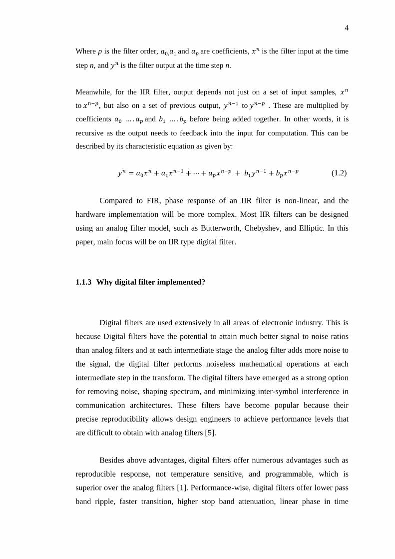
Where p is the filter order, 𝑎 𝑎 and 𝑎 are coefficients, is the filter input at the time
step n, and is the filter output at the time step n.
Meanwhile, for the IIR filter, output depends not just on a set of input samples,
to , but also on a set of previous output, to . These are multiplied by
coefficients 𝑎 𝑎 and before being added together. In other words, it is
recursive as the output needs to feedback into the input for computation. This can be
described by its characteristic equation as given by:
𝑎 𝑎
𝑎
(1.2)
Compared to FIR, phase response of an IIR filter is non-linear, and the
hardware implementation will be more complex. Most IIR filters can be designed
using an analog filter model, such as Butterworth, Chebyshev, and Elliptic. In this
paper, main focus will be on IIR type digital filter.
1.1.3 Why digital filter implemented?
Digital filters are used extensively in all areas of electronic industry. This is
because Digital filters have the potential to attain much better signal to noise ratios
than analog filters and at each intermediate stage the analog filter adds more noise to
the signal, the digital filter performs noiseless mathematical operations at each
intermediate step in the transform. The digital filters have emerged as a strong option
for removing noise, shaping spectrum, and minimizing inter-symbol interference in
communication architectures. These filters have become popular because their
precise reproducibility allows design engineers to achieve performance levels that
are difficult to obtain with analog filters [5].
Besides above advantages, digital filters offer numerous advantages such as
reproducible response, not temperature sensitive, and programmable, which is
superior over the analog filters [1]. Performance-wise, digital filters offer lower pass
band ripple, faster transition, higher stop band attenuation, linear phase in time

5
domain over its analog counterpart. Besides, digital filters are able to take full
advantage of the advanced submicron technology that IC chip makers are able to
offer today. Nevertheless, the downside of digital filter is the aliasing of digital signal
caused by sampling effects. Unlike analog filter, digital filter are unable to pass
power and requires a power supply. It might also encounter interference where out-
of-band signals are frequency shifted and appear in the pass band. Applications of
digital filtering are enormous, including noise suppression in consumer electronics,
selectively filtering electrical signals such as brain, heart, neurological signals from
human body in biomedical applications, image enhancements of high frequency
image elements, bandwidth limiting of intended television and radio signals in
communications and many more [1].
Digital processing of continuous signals Digital signal processing has very
broad application areas, ranging from simulation of analog (continuous) networks on
digital computers to the development of new digital systems that will completely
replace analogue. There are many advantages of digital over analog signal
processing. Digital signal processing can be realized with higher degree of accuracy.
Then, one computer can simultaneously perform multiple digital signal processing's.
Digital networks are very flexible, easily can be changed by changing the program
parameters [4].
1.1.4 Why IIR instead of FIR
Infinite impulse response (IIR) filters are widely used in digital signal
processing systems due to the following causes. IIR filters are rigorously analogous
to well-known and widely used analog filters. Finite impulse response filters (FIR)
have computational complexity several times as much as IIR filters have. In most
cases IIR filters are implemented by signal processors and ASICs, which architecture
is adapted to filtering algorithms. For a long time IIR filters represent applications of
FPGAs in the digital signal processing [6]. Implementation IIR filters in FPGA has a
set of advantages, such as full adaptation of implemented in FPGA structure to the
filtering algorithm, high throughput, hardware utilization effectiveness, achieving
6
high rate of calculating precision. In many special applications, like high speed
communications, image computing FPGA is the only solution for IIR filters
implementation. In the representation data flow graphs (DFG) for IIR filtering
algorithm, its optimization, and mapping into the structure are considered taking into
account structure forming properties of modern FPGAs [7].
1.2 Why FPGA
In some high performance applications, an FPGA or ASIC is used instead of a
general purpose microprocessor. FPGA becomes a platform of choice for hardware
realization of computation-intensive algorithms due to
• Design flexibility due to its re-configurable/programmable
• Rapid prototyping of complex algorithms
• Simplifies debugging and verifications
• Able to develop hardware design techniques such as parallelism and
pipelining
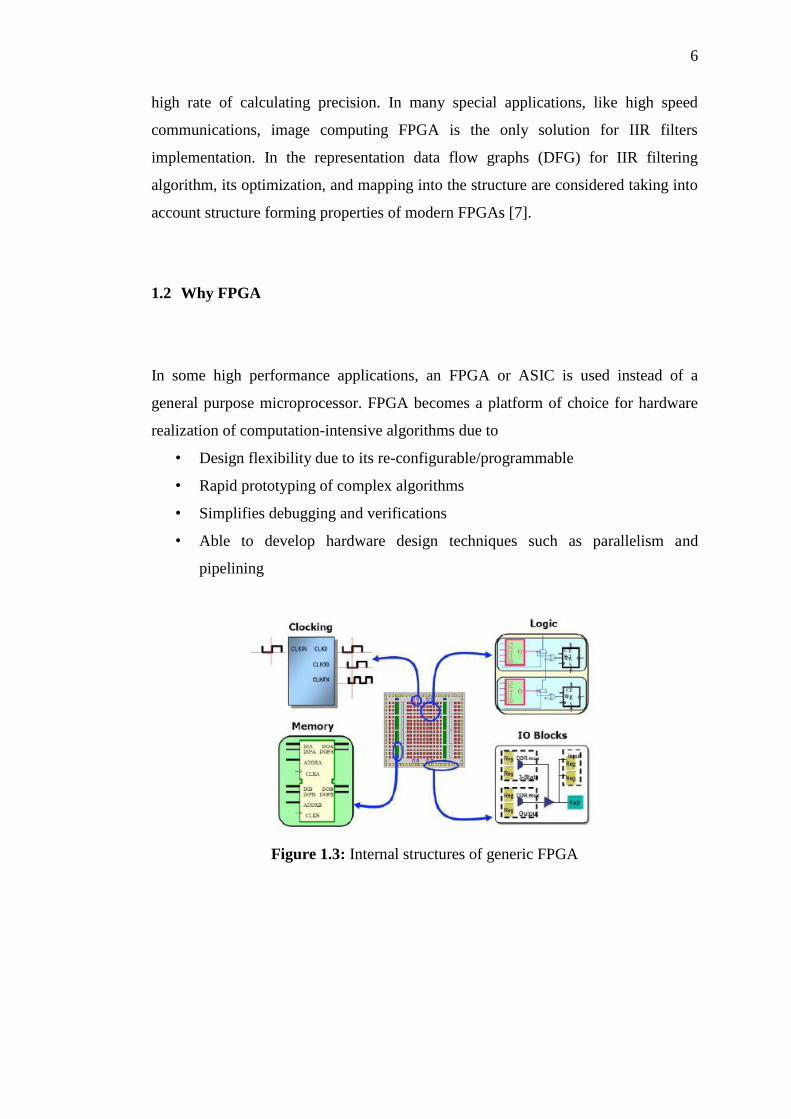
Figure 1.3: Internal structures of generic FPGA

7
1.3 Design challenging
Characteristics of digital networks are stable, and reliability is great. We
should not neglect the fact that the price of digital components is significantly lower
than the cost of analog components. In terms of physical dimensions of the networks
the advantage is also on the digital processing side. The limitation of digital networks
is that the signal processing takes some time. Also, the use of digital networks for
processing high frequency digital signals is limited. Besides the limitations related to
the speed of digital signal processing digital networks have more drawbacks, such as
the existence of the noise and low dynamic of the signal. Noise cannot be avoided
because it occurs as a result of signal quantization, rounding of the product and
rounding of the sum in the numerical calculations. Noise reducing and increasing of
the signal dynamic can be achieved by increasing the length of digital words which
are used to represent numbers. However, the speed of filter reduces with digital word
length increasing. It is therefore necessary to find compromise between the filter
speed and the size of the noise generated by digital network [2].
These devices are extremely flexible, but are limited in performance. High
performance designs for filtering at sampling rates above 100 MHz have been
demonstrated using CMOS [8] and Bi-CMOS [8] technologies. In this research the
same performance can be achieved by structuring the architecture based on correct
approach in FPGA, these efforts expected to produce high performance filter designs
for specific application domains.
Although nowadays more than 500 DSP blocks available, and even very large
order filters can sustain input sampling rates over 400 MHz and the performance far
exceeds even the fastest DSP processors by orders of magnitude, in this research we
more focused to solve the objectives by targeting the performance at 200 MHz and to
bring the existing work into the hardware realization FPGA.
8
1.4 Problem statements
Based on the paper “Hardware Implementation Analysis for Digital Filters”
and “An approach to Digital Low-Pass IIR Filter Design” they are limitation on the
high performance digital filter sampling frequency.
According to the paper “FPGA IMPLEMENTATION OF DIGITAL
FILTERS” high performance design can be categorized when the sampling rate
100Mhz, and for filtering at sampling rates above 100 MHz have also been
demonstrated using CMOS and Bi-CMOS technologies, using approaches ranging
from full custom to traditional factory-configured gate arrays.
Therefore this research interest is to design the high performance IIR digital
filter using the same approach BiQuad architecture and FPGA cyclone II family
benchmark with the current design on paper “FPGA IMPLEMENTATION OF
DIGITAL FILTERS”
1.5 Research objectives
To explore the three architectures of high performance IIR Band Stop filter in
FPGA using the 2nd order of BiQuad architecture and cyclone II device FPGA
family.
Band stop IIR Filter design specifications are tested:
Butterworth filter
BiQuad 2nd order
Cutoff Frequency 1 = 6 kHz
Cutoff Frequency 2 = 15kHz
We will only focus on band stop but can easily be extended to any different
digital filters but restricted to IIR
9
1.6 Research Motivation and Objectives
Research on digital filter implementation over the years has concentrated on
custom implementation using various ASIC technologies. Several potential
shortcomings of custom Very-Large-Scale Integration (VLSI) ASIC approach [1]:
Lack of flexibility in custom approach – Custom devices are often suited only
for use in particular application, not reconfigurable.
Forestall the cost effective evaluation – Only high volume applications or
extremely low volume applications can justify the expense of developing a
full custom solution.
Lack of adaptability – Does not allow user to modify the function of a device.
Lack of report of filter algorithm to implement in FPGA.
Although these problems can be overcome with sufficient forethought, the
costs in performance, design complexity, and additional design time often preclude
flexible solutions. Field Programmable Gate Arrays (FPGAs) can be used to alleviate
some of the problems with custom approach as they are programmable logic devices.
In-system programmable allows modification of the operation of the device through
simple reprogramming.
Therefore, the objective of this project is to illustrate the approaches in designing
modern digital filters in FPGA as listed below:
1) Single cycle (concurrent)
2) Multi Cycle (resource constraints)
3) Pipelined
This research was not the first time carried out, but it is leverage from
previous master student work. The previous work more to the study of the digital
filter, approaches, and also finding the suitable architecture. Therefore in this
extended research, the focus more the higher performance digital filter design with
target specs is 200 Mhz operating frequency and its can sustains the sampling rates

10
maximum 200 Mhz with the execution time is 0.5ns per input. All design will be
modeled and synthesized using Quartus II and quantitative measurement will be
provided in terms of performance. In order to further improve the design and make
full use of the capability of FPGA, general multipliers and ALU will be used based
on compatible in FPGA library.
1.7 Design Outcome and Expected Contribution
The outcome and contribution of the project is to meet the demand for the
development of courseware in the teaching unit of department of computer and
Electrical-Microelectronics Engineering. There are several results have been
achieved through the previous projects which are:
1. A study of design procedures from different approaches. There is
more than one way to implement the digital IIR filter.
2. The purpose of the project is to identify the different approaches
compare and contrast the different methods, so based on the design
specification; careful choice of implementation method can save
designer a lot of time and work.
3. To investigate relationship hardware architecture and FPGA resources
usage and Quartus II as major design tool to design filters then
compare and contrast the outcome from Matlab.
4. In further study in part two, will get to know how to design the system
in FPGA and the real world design prototype is created. This design is
fully embedded.
5. Get to learn the Verilog High Level System Language which is more
crucial in nowadays industry.
11
1.8 Scope of work
The scope of work is to implement and to carry out the IIR filter
determination and hardware realizations. This is to create the real world prototype
from the previous design work. From these research also three architectures of high
performance IIR Band Stop filter in FPGA using the 2nd order of BiQuad
architecture and cyclone II device FPGA family was explored.
This project starts off with a brief introduction of digital filter and FPGA,
followed by the motivations and objectives of this project in Chapter 1. In Chapter 2,
there will be literature research to understand the underlying principle of digital
filtering and the limitations of digital quantization, before reviewing the proposed
BiQuad hardware architecture methodologies and its FPGA implementation in this
project. As progress into Chapter 3, the methodology and implementation plan to
carry out the filter determination and hardware realizations will be discussed, at the
same time explaining about the software tools, namely Matlab & Quartus II, which
will be using extensively to aid the analysis and development. Based on the
simulation, bit true model of sample digital filter will be extracted and the BiQuad
hardware design will be implemented based on the proposed methodologies in
Chapter 4. The methodologies are: Single Cycle, Multi Cycle (resource constraints)
and pipelined. Besides, the filter design will be further optimized on the stored
computed coefficients. Each hardware design will be explored by realizing its RTL
designs. Subsequently, the preliminary results of the hardware implementation will
be discussed, by comparing the performance in Chapter 5.
71
REFERENCES
[1] Ow, Shen Wah, “STUDY ON FPGA BASED IIR FILTER USING
QUANTITATIVE APPROACH”, 2012.
[2] Michael Francis, “Infinite Impulse Response Filter Structures in Xilinx
FPGAs”, White Paper: "Spartan®-3A DSP, Virtex®-5/Virtex-4 FPGAs,
LogiCORE™ IP. WP330 (v1.2) August 10, 2009
[3] http://en.wikipedia.org/wiki/Digital_filter
[4] Bojan Jovanović, and Milun Jevtić, “An approach to Digital Low-Pass IIR
Filter Design”, Department of Electronics, Faculty of Electronic Engineering,
University of Niš, Aleksandra Medvedeva 14, 18000 Niš, Serbia, 12-14 February
2010
[5] Yishu Wang, “Implementation of digital filter by using FPGA”, School of
Electrical and Computer Engineering Curtin University, 2005.
[6] J. Isoaho, J. Pasawn, O. Vaino, H. Terhunen. DSP System Integration and
Prototyping with FPGAs. J. VLSI Signal Processing, 1993, ą 6, p. 155-172.
[7] Anatoli Sergyienko, Volodymir Lepekha, Juri Kanevski, Przemyslaw Soltan,
“IMPLEMENTATION OF IIR DIGITAL FILTERS IN FPGA”, National
Technical University of Ukraine.
[8] Chi-Jui Chou, Satish Mohanakrishnan, Joseph B. Evans, “FPGA
IMPLEMENTATION OF DIGITAL FILTERS”, Telecommunications&
Information Sciences Laboratory Department of Electrical & Computer
Engineering University of Kansas, 1993.
[9] F. T. Arthur Williams, Electronic Filter Design Handbook, Fourth Edition,
McGraw-Hill Handbooks, July 10, 2006.

72
[10] C. J. W. Alan V. Oppenheim, "Effects of Finite Register Length in Digital
Filtering and the Fast Fourier Transform," Proeedings of the IEEE, vol. 60, no. 8,
pp. 957 - 976, Aug. 1972.
[11] J. Serrano, "Introduction to FPGA design," CAS - CERN Accelerator School:
Course on Digital Signal Processing, pp. 231-247, 2007.
[12] Response Digital Filters," 15th Symposium on Integrated Circuits and Systems
Design 2002, pp. 20-25, Sep. 2002.
[13] J. M. G. L. Y. Y. Roger Woods, FPGA-based Implementation of Signal
Processing Systems, United Kingdom: A John Wiley and Sons, Ltd., Publication,
2008.
[14] K. a. K. P. Tracy C. Denk, "Exhaustive scheduling and retiming of digital signal
processing systems," IEEE Transactions on Circuits and Systems-II: Analog and
Digital Signal Processing, vol. 45, no. 7, Jul. 1998.
[15] S. Y. C. Pradabpet, "Design and implementation of biquad digital filter," The 9th
Asia-Pacific Conference on Communications 2003 (APCC 2003), vol. 3, Sep. 2003.
[16] RIK VLAMINCK1, JO PLETINCKX2, STEFAAN VERSCHUERE1, STIJN
BERTREM1, JAN VANDEWEGE1, PATRICK BOETS3, GUNTER VANUYTSEL3 ,
SERGE TEMMERMAN, “FPGA based real-time constrained time area optimized IIR
design using digit-serial arithmetic”, INTEC design, Ghent University
[17] N. M. M. S. M. F. Hamed Hollisaz, "A Quantitative Approach to Digital Filter
Implementation," Microelectronics, 2005. ICM 2005. The 17th International
Conference on , pp. 160 - 164, 2005.
[18] S. R. a. S. M. F. N. Sedaghati-Mokhtari, "HARDWARE IMPLEMENTATION
ANALYSIS FOR DIGITAL FILTERS," Iranian Conference on Electrical
Engineering (ICEE) 2006 , 2006.
[19] Mohammad Shajaan and John Aasted Sgwensen, “TIME-AREA EFFICIENT
MULTIPLIER-FREE RECURSIVE FILTER ARCHITECTURES FOR FPGA
IMPLEMENTATION” Technical University of Denmark, 1996.
[20] Altera Manual on Design Debugging Using the SignalTap II Logic Analyzer