Embed Size (px)
Citation preview
High-Performance Data Converters
by
Jesper Steensgaard-Madsen
A thesis submitted in partial fulfillment of
the requirementments for the Ph.D. degree
The Technical University of Denmark
Department of Information Technology
DK-2800, Lyngby Denmark
January 20, 1999
(Revised March 8, 1999)
c by Jesper Steensgaard-Madsen, 1999


Copyright c
by Jesper Steensgaard-Madsen, 1999
All rights reserved

Abstract
Novel techniques for multi-bit oversampled data conversion are described. State-of-the-art oversam-
pled data converters are analyzed, leading to the conclusion that their performance is limited mainly
by low-resolution signal representation. To increase the resolution, high-performance, high-resolution
internal D/A converters are required. Unit-element mismatch-shaping D/A converters are analyzed, and
the concept of mismatch-shaping is generalized to include scaled-element D/A converters. Several types
of scaled-element mismatch-shaping D/A converters are proposed. Simulations show that, when imple-
mented in a standard CMOS technology, they can be designed to yield 100 dB performance at 10 times
oversampling.
The proposed scaled-element mismatch-shaping D/A converters are well suited for use as the feedback
stage in oversampled delta-sigma quantizers. It is, however, not easy to make full use of their potential,
because that requires a high-resolution loop quantizer which introduces only a small delay. Generally, it
is not acceptable to design the loop quantizer as a high-resolution flash quantizer because they require a
large chip area and high power consumption. Pipeline techniques are proposed to circumvent this prob-
lem. This way, the delta-sigma quantizer’s feedback signal is obtained by a multiple-stage quantization,
where the loop quantizer (low-resolution and minimum-delay) implements only the last-stage quanti-
zation. Hence, high-speed, high-resolution delta-sigma quantization is feasible without using complex
circuitry.
An improved version of the MASH topology is also proposed. A delta-sigma quantizer is used to quan-
tize the input signal into an oversampled digital representation of low-to-moderate resolution. The delta-
i

ii
sigma quantizer’s truncation error is estimated either directly, or as the first-order difference of the output
signal from the loop filter’s first integrator stage. This technique avoids the need for accurate matching
of analog and digital filters that characterizes the MASH topology, and it preserves the signal-band
suppression of quantization errors. Simulations show that quantizers of this type can yield 100 dB per-
formance at 10 times oversampling. There are no requirements for high-resolution flash quantizers or
other hard-to-implement circuitry.
Acknowledgements
The author wishes to acknowledge several people for their contributions to this work.
In a category by himself, Professor Gabor C. Temes has helped me in countless ways during the almost
two years I have been fortunate enough to work with him. I thank him for his friendship, encouragement,
advice, enthusiasm, ideas, feedback, editing, our discussions, and for providing an environment where
electrical engineering can be practiced in a fun and rewarding way. He truly deserves the “IEEE Graduate
Teaching Award,” which was awarded to him in 1998. He has my highest respect and appreciation in
every aspect.
At Oregon State University I have worked with many wonderful people with whom I have had fruitful
discussions. They have included Professor Un-Ku Moon, Professor Richard Schreier, Luis Hernandez,
Andreas Wiesbauer, Paul Ferguson, Yunteng Huang, Bo Wang, Tao Sun, and many more.
I particularly wish to thank the President of MEAD Microelectronics Inc. of Switzerland, Vlado Valence,
and Gabor and Ibi Temes, from U.S. MEAD, for inviting me to participate in the outstanding courses
in electrical engineering which they arrange in Switzerland and in the United States. I believe I have
obtained some of my most useful and practical information from these courses, and I am very grateful
for that. I need to thank the outstanding course lecturers who teach these courses, many of whom I have
been fortunate to encounter in private and fruitful discussions. In arbitrary order, I particularly wish
to thank Bob Adams, Eric Vittoz, Paul Brokaw, Tim Schmerbeck, Christian Enz, Todd Brooks, Paul
Ferguson, Bob Blauschild, Ian Galton, Berrie Gilbert, Stephen Jantzi and several others.
iii

iv
I also extend my thanks to the design team at MEAD Microelectronics Inc., particularly Fabien and
Phillip Duval.
For making my life pleasant in many ways, I wish to thank my brother, Bjarne, his wife, Tamara, and
my girlfriend, Patrice. Also, I wish to thank Ms. Ibi Temes for her gracious hospitality at the Temes’
home on several occasions.
Finally, I wish to thank my supervisor, Erik Bruun, and the Danish educational system for its financial
support.

Contents
1 Introduction 1
1.1 The Class of Data Converters Considered . . . . . . . . . . . . . . . . . . . . . . . . . 3
1.2 The Structure of This Thesis . . . . . . . . . . . . . . . . . . . . . . . . . . . . . . . . 6
1.3 Intellectual Property Rights . . . . . . . . . . . . . . . . . . . . . . . . . . . . . . . . . 7
2 Characterization of Signals 9
2.1 Time-Domain Representation of Signals . . . . . . . . . . . . . . . . . . . . . . . . . . 9
2.1.1 Analog Signals . . . . . . . . . . . . . . . . . . . . . . . . . . . . . . . . . . . 10
2.1.2 Digital Signals . . . . . . . . . . . . . . . . . . . . . . . . . . . . . . . . . . . 11
2.2 Frequency-Domain Representation of Signals . . . . . . . . . . . . . . . . . . . . . . . 12
2.2.1 Fourier Transformation of Continuous-Time Signals . . . . . . . . . . . . . . . 13
2.2.2 Fourier Transformation of Discrete-Time Signals . . . . . . . . . . . . . . . . . 14
2.2.3 Definition of the Signal Band . . . . . . . . . . . . . . . . . . . . . . . . . . . 16
2.2.4 Nyquist’s Sampling Theorem . . . . . . . . . . . . . . . . . . . . . . . . . . . 17
2.2.5 Aliasing . . . . . . . . . . . . . . . . . . . . . . . . . . . . . . . . . . . . . . . 18
v
vi CONTENTS
2.3 Estimation of a Signal’s Fourier Spectrum . . . . . . . . . . . . . . . . . . . . . . . . . 18
2.3.1 Estimation Based on a Finite-Duration Signal . . . . . . . . . . . . . . . . . . . 19
2.3.2 Estimation Based on Assumed Periodicity . . . . . . . . . . . . . . . . . . . . . 21
2.3.3 The Discrete Fourier Transformation . . . . . . . . . . . . . . . . . . . . . . . 23
3 Basic Aspects of Data Conversion 29
3.1 Fundamental Steps in A/D Conversion . . . . . . . . . . . . . . . . . . . . . . . . . . . 29
3.1.1 Errors Caused by the Anti-Aliasing Filter . . . . . . . . . . . . . . . . . . . . . 30
3.1.2 Errors Caused by the Sample-and-Hold Circuit . . . . . . . . . . . . . . . . . . 33
3.1.3 Characterization of the Ideal Quantizer . . . . . . . . . . . . . . . . . . . . . . 35
3.1.4 Characterization of Quantizer Errors . . . . . . . . . . . . . . . . . . . . . . . . 39
3.2 Fundamental Steps in D/A Conversion . . . . . . . . . . . . . . . . . . . . . . . . . . . 42
3.2.1 Basic Voltage-Mode Implementation . . . . . . . . . . . . . . . . . . . . . . . 42
3.2.2 Basic Current-Mode Implementation . . . . . . . . . . . . . . . . . . . . . . . 45
3.2.3 Clock Jitter in D/A Converters . . . . . . . . . . . . . . . . . . . . . . . . . . . 49
3.2.4 Static Performance of D/A Converters . . . . . . . . . . . . . . . . . . . . . . . 53
3.2.5 Linearity Limitations . . . . . . . . . . . . . . . . . . . . . . . . . . . . . . . . 55
3.3 Measuring Dynamic Performance . . . . . . . . . . . . . . . . . . . . . . . . . . . . . 60
3.3.1 Signal-to-Noise Ratio . . . . . . . . . . . . . . . . . . . . . . . . . . . . . . . 61
3.3.2 Dynamic Range . . . . . . . . . . . . . . . . . . . . . . . . . . . . . . . . . . . 61
3.3.3 Spurious-Free Dynamic Range . . . . . . . . . . . . . . . . . . . . . . . . . . . 62

CONTENTS vii
3.3.4 Intermodulation Distortion . . . . . . . . . . . . . . . . . . . . . . . . . . . . . 62
3.4 Quantizer Topologies . . . . . . . . . . . . . . . . . . . . . . . . . . . . . . . . . . . . 62
3.4.1 Direct-Comparison Data Quantizers . . . . . . . . . . . . . . . . . . . . . . . . 63
3.4.2 Residue-Calculating Data Quantizers . . . . . . . . . . . . . . . . . . . . . . . 65
3.4.3 Introduction to Signal Quantizers . . . . . . . . . . . . . . . . . . . . . . . . . 71
4 State-of-the-Art Signal Quantizers 79
4.1 Single-Bit Delta-Sigma Quantizers . . . . . . . . . . . . . . . . . . . . . . . . . . . . . 80
4.1.1 Obtaining and Preserving Stability . . . . . . . . . . . . . . . . . . . . . . . . . 81
4.1.2 Bandwidth Limitation . . . . . . . . . . . . . . . . . . . . . . . . . . . . . . . 86
4.2 MASH Topology . . . . . . . . . . . . . . . . . . . . . . . . . . . . . . . . . . . . . . 87
4.2.1 Analysis of the MASH Topology . . . . . . . . . . . . . . . . . . . . . . . . . 88
4.3 Multi-Bit Delta-Sigma Quantizers . . . . . . . . . . . . . . . . . . . . . . . . . . . . . 92
4.3.1 Stability Properties . . . . . . . . . . . . . . . . . . . . . . . . . . . . . . . . . 93
4.4 Mismatch-Shaping DACs . . . . . . . . . . . . . . . . . . . . . . . . . . . . . . . . . . 97
4.4.1 Estimation of the Error Signal . . . . . . . . . . . . . . . . . . . . . . . . . . . 98
4.4.2 First-Order Unit-Element Mismatch-Shaping DACs . . . . . . . . . . . . . . . . 100
4.4.3 Performance of First-Order Mismatch-Shaping DACs . . . . . . . . . . . . . . . 105
4.4.4 Second-Order Mismatch-Shaping DACs . . . . . . . . . . . . . . . . . . . . . . 110
4.4.5 Performance of Second-Order Mismatch-Shaping DACs . . . . . . . . . . . . . 116
4.4.6 Mismatch-Shaping Encoders in Perspective . . . . . . . . . . . . . . . . . . . . 120

viii CONTENTS
4.5 Noise Limitation . . . . . . . . . . . . . . . . . . . . . . . . . . . . . . . . . . . . . . 121
4.5.1 Discrete-Time Delta-Sigma Quantizers . . . . . . . . . . . . . . . . . . . . . . 121
4.5.2 Continuous-Time Delta-Sigma Quantizers . . . . . . . . . . . . . . . . . . . . . 124
4.5.3 Conclusion . . . . . . . . . . . . . . . . . . . . . . . . . . . . . . . . . . . . . 132
5 Improved Current-Mode DACs 133
5.1 Dual Return-to-Zero Current-Mode DAC . . . . . . . . . . . . . . . . . . . . . . . . . 133
5.1.1 A Variation . . . . . . . . . . . . . . . . . . . . . . . . . . . . . . . . . . . . . 136
5.2 Time-Interleaved Current-Mode DAC . . . . . . . . . . . . . . . . . . . . . . . . . . . 136
5.2.1 Basic Topology and Operation . . . . . . . . . . . . . . . . . . . . . . . . . . . 137
5.2.2 Analysis . . . . . . . . . . . . . . . . . . . . . . . . . . . . . . . . . . . . . . 139
5.3 Conclusion . . . . . . . . . . . . . . . . . . . . . . . . . . . . . . . . . . . . . . . . . 140
6 Dithering of Mismatch-Shaping DACs 143
6.1 Idle Tones in Deterministic UE-MS Encoders . . . . . . . . . . . . . . . . . . . . . . . 143
6.1.1 Idle Tones in ERS UE-MS Encoders . . . . . . . . . . . . . . . . . . . . . . . . 144
6.1.2 Idle Tones in Complex UE-MS Encoders . . . . . . . . . . . . . . . . . . . . . 146
6.2 Dithered UE-MS Encoders . . . . . . . . . . . . . . . . . . . . . . . . . . . . . . . . . 147
6.2.1 Dithered Tree-Structure UE-MS Encoders . . . . . . . . . . . . . . . . . . . . . 148
6.2.2 Dithered ERS UE-MS Encoders . . . . . . . . . . . . . . . . . . . . . . . . . . 151
6.3 Random-Orientation Dithered ERS Encoder . . . . . . . . . . . . . . . . . . . . . . . . 154
6.3.1 A Family of Dithering Techniques . . . . . . . . . . . . . . . . . . . . . . . . . 158

CONTENTS ix
6.3.2 Random-Rotation-Scheme Dithering . . . . . . . . . . . . . . . . . . . . . . . . 160
6.4 Conclusion . . . . . . . . . . . . . . . . . . . . . . . . . . . . . . . . . . . . . . . . . 161
7 Scaled-Element Mismatch-Shaping D/A Converters 165
7.1 High-Resolution Mismatch-Shaping DACs . . . . . . . . . . . . . . . . . . . . . . . . . 166
7.1.1 General Aspect of the Design of Mismatch-Shaping Encoders . . . . . . . . . . 166
7.1.2 Mismatch-shaping Unit-Element DACs – Revisited . . . . . . . . . . . . . . . . 168
7.1.3 Complicated Scaled-Element Mismatch-Shaping Encoders . . . . . . . . . . . . 168
7.1.4 Simple Scaled-Element Mismatch-Shaping Encoders . . . . . . . . . . . . . . . 169
7.2 A Dual-Type-Element Mismatch-Shaping DAC . . . . . . . . . . . . . . . . . . . . . . 171
7.2.1 Designing the Delta-Sigma Modulator . . . . . . . . . . . . . . . . . . . . . . . 172
7.2.2 Parallel Work Published . . . . . . . . . . . . . . . . . . . . . . . . . . . . . . 174
7.3 Tree-Structure Scaled-Element Mismatch-Shaping DACs . . . . . . . . . . . . . . . . . 176
7.3.1 Asymmetrical Tree Structures . . . . . . . . . . . . . . . . . . . . . . . . . . . 178
7.3.2 One-Sided Tree-Structure . . . . . . . . . . . . . . . . . . . . . . . . . . . . . 180
7.4 Filtering Scaled-Element Mismatch-Shaping DACs . . . . . . . . . . . . . . . . . . . . 182
7.4.1 Minimalist Scaled-Element Mismatch-Shaping Encoder . . . . . . . . . . . . . 183
7.4.2 Practical Filtering Scaled-Element Mismatch-Shaping DACs . . . . . . . . . . . 184
7.4.3 Reducing the Gain-Error Sensitivity . . . . . . . . . . . . . . . . . . . . . . . . 185
7.5 Second-Order Scaled-Element Mismatch-Shaping DACs . . . . . . . . . . . . . . . . . 189
7.5.1 The Generalized Filtering Principle . . . . . . . . . . . . . . . . . . . . . . . . 189
x CONTENTS
7.5.2 The Filter-Mismatch Problem . . . . . . . . . . . . . . . . . . . . . . . . . . . 191
7.5.3 Variations . . . . . . . . . . . . . . . . . . . . . . . . . . . . . . . . . . . . . . 192
7.5.4 Switched-Capacitor Implementation . . . . . . . . . . . . . . . . . . . . . . . . 193
7.5.5 Linear Three-Level DACs . . . . . . . . . . . . . . . . . . . . . . . . . . . . . 201
7.5.6 Current-Mode Implementation . . . . . . . . . . . . . . . . . . . . . . . . . . . 206
7.5.7 Mismatch-Shaping Bandpass DACs . . . . . . . . . . . . . . . . . . . . . . . . 210
8 High-Resolution Delta-Sigma Quantizers 211
8.1 Choosing the Optimal Resolution . . . . . . . . . . . . . . . . . . . . . . . . . . . . . . 212
8.1.1 Fundamental Principle for High-Resolution Quantization . . . . . . . . . . . . . 213
8.2 Two-Stage Delta-Sigma Quantizers . . . . . . . . . . . . . . . . . . . . . . . . . . . . . 213
8.2.1 Preventing Nonlinearity . . . . . . . . . . . . . . . . . . . . . . . . . . . . . . 216
8.2.2 Simulation Results . . . . . . . . . . . . . . . . . . . . . . . . . . . . . . . . . 217
8.3 Implementation of Two-Stage Delta-Sigma Quantizers . . . . . . . . . . . . . . . . . . 219
8.3.1 Introducing Pipeline Techniques to Allow Circuit Delays . . . . . . . . . . . . . 221
8.3.2 Design of Analog Delay Lines . . . . . . . . . . . . . . . . . . . . . . . . . . . 222
8.3.3 Avoiding Sequential Settling . . . . . . . . . . . . . . . . . . . . . . . . . . . . 225
8.3.4 Proposed Circuit-Level Implementation . . . . . . . . . . . . . . . . . . . . . . 226
9 Residue-Compensated Delta-Sigma Quantizers 233
9.1 Directly Residue-Compensated Delta-Sigma Quantizers . . . . . . . . . . . . . . . . . . 234
9.1.1 Analysis and Performance Evaluation . . . . . . . . . . . . . . . . . . . . . . . 234
CONTENTS xi
9.2 Indirectly Residue-Compensated Delta-Sigma Quantizers . . . . . . . . . . . . . . . . . 236
9.2.1 Analysis and Performance Evaluation . . . . . . . . . . . . . . . . . . . . . . . 238
9.2.2 Controlling the Residue-Quantization Error . . . . . . . . . . . . . . . . . . . . 239
9.2.3 Controlling the Filter-Mismatch-Induced Error . . . . . . . . . . . . . . . . . . 244
9.2.4 Designing Residue-Compensated Delta-Sigma Quantizers . . . . . . . . . . . . 248
9.3 Continuous-Time Delta-Sigma Quantizers . . . . . . . . . . . . . . . . . . . . . . . . . 250
9.3.1 High-Resolution Continuous-Time Delta-Sigma Quantizers . . . . . . . . . . . 250
9.3.2 Residue-Compensated Continuous-Time �� Quantizers . . . . . . . . . . . . . 253
9.3.3 Conclusions . . . . . . . . . . . . . . . . . . . . . . . . . . . . . . . . . . . . . 257
10 Conclusion 259

xii CONTENTS

List of Figures
2.1 DT/CT conversions commonly used for signal analysis . . . . . . . . . . . . . . . . . . 15
2.2 A graphic interpretation of aliasing . . . . . . . . . . . . . . . . . . . . . . . . . . . . . 15
2.3 The Fourier transform (magnitude) of the rectangular window . . . . . . . . . . . . . . 20
2.4 The observed frequency spectrum of a two-tone periodic signal . . . . . . . . . . . . . . 20
2.5 Fundamental steps in the band-pass-filter method . . . . . . . . . . . . . . . . . . . . . 22
2.6 Examples of DTFs that are subject to spectral leakage . . . . . . . . . . . . . . . . . . . 27
3.1 Fundamental steps in A/D conversion . . . . . . . . . . . . . . . . . . . . . . . . . . . 30
3.2 Aliasing errors . . . . . . . . . . . . . . . . . . . . . . . . . . . . . . . . . . . . . . . 32
3.3 Clock-jitter errors (sampling) . . . . . . . . . . . . . . . . . . . . . . . . . . . . . . . . 35
3.4 Static characteristic for linear quantizers . . . . . . . . . . . . . . . . . . . . . . . . . . 36
3.5 Residue of an ideal quantizer . . . . . . . . . . . . . . . . . . . . . . . . . . . . . . . . 37
3.6 Quantizer model . . . . . . . . . . . . . . . . . . . . . . . . . . . . . . . . . . . . . . . 38
3.7 Static characteristic of a nonideal quantizer . . . . . . . . . . . . . . . . . . . . . . . . 39
3.8 Voltage-mode D/A converter system . . . . . . . . . . . . . . . . . . . . . . . . . . . . 42
xiii
xiv LIST OF FIGURES
3.9 Output stage of a single-bit delta-sigma D/A converter . . . . . . . . . . . . . . . . . . 44
3.10 Current-mode D/A converter system . . . . . . . . . . . . . . . . . . . . . . . . . . . . 45
3.11 Current-steering D/A converter . . . . . . . . . . . . . . . . . . . . . . . . . . . . . . . 46
3.12 Dynamic errors in a current-mode D/A converter . . . . . . . . . . . . . . . . . . . . . 47
3.13 Return-to-zero switching scheme . . . . . . . . . . . . . . . . . . . . . . . . . . . . . . 49
3.14 Clock jitter errors (reconstruction) . . . . . . . . . . . . . . . . . . . . . . . . . . . . . 50
3.15 Static characteristic of an nonideal D/A converter . . . . . . . . . . . . . . . . . . . . . 54
3.16 Topology of most D/A converters . . . . . . . . . . . . . . . . . . . . . . . . . . . . . . 55
3.17 Basic residue stage . . . . . . . . . . . . . . . . . . . . . . . . . . . . . . . . . . . . . 66
3.18 Two-step flash quantizer . . . . . . . . . . . . . . . . . . . . . . . . . . . . . . . . . . 67
3.19 Scaled two-step flash quantizer . . . . . . . . . . . . . . . . . . . . . . . . . . . . . . . 68
3.20 Four-stage pipeline quantizer . . . . . . . . . . . . . . . . . . . . . . . . . . . . . . . . 70
3.21 Fundamental principle of signal quantizers . . . . . . . . . . . . . . . . . . . . . . . . . 71
3.22 Signal quantizer with a nonideal feedback D/A converter . . . . . . . . . . . . . . . . . 72
3.23 Fundamental elements in a smart quantizer . . . . . . . . . . . . . . . . . . . . . . . . . 74
3.24 Typical (delta-sigma) signal quantizer . . . . . . . . . . . . . . . . . . . . . . . . . . . 75
3.25 Optimized (delta-sigma) signal quantizer . . . . . . . . . . . . . . . . . . . . . . . . . . 76
3.26 Interpretation of (delta-sigma) signal quantizers . . . . . . . . . . . . . . . . . . . . . . 77
4.1 Single-bit delta-sigma A/D converter system . . . . . . . . . . . . . . . . . . . . . . . . 81
4.2 Linear model of a delta-sigma loop . . . . . . . . . . . . . . . . . . . . . . . . . . . . . 82
LIST OF FIGURES xv
4.3 Nonlinear model of a delta-sigma loop . . . . . . . . . . . . . . . . . . . . . . . . . . . 83
4.4 Delta-sigma loop filter . . . . . . . . . . . . . . . . . . . . . . . . . . . . . . . . . . . 84
4.5 MASH-topology delta-sigma quantizer . . . . . . . . . . . . . . . . . . . . . . . . . . . 88
4.6 Time-domain output from two multi-bit delta-sigma quantizers. . . . . . . . . . . . . . . 94
4.7 Conceptual mismatch-shaping D/A converter . . . . . . . . . . . . . . . . . . . . . . . 98
4.8 Topology of most mismatch-shaping D/A converters . . . . . . . . . . . . . . . . . . . 99
4.9 Element-rotation scheme . . . . . . . . . . . . . . . . . . . . . . . . . . . . . . . . . . 104
4.10 Implementation of the element-rotation scheme . . . . . . . . . . . . . . . . . . . . . . 104
4.11 Signal-band power of differentiated white-noise errors . . . . . . . . . . . . . . . . . . 108
4.12 Symbol for UE-MS D/A converters . . . . . . . . . . . . . . . . . . . . . . . . . . . . 111
4.13 Transformation used for tree-structure UE-MS D/A converters . . . . . . . . . . . . . . 112
4.14 Tree-structured UE-MS D/A converter . . . . . . . . . . . . . . . . . . . . . . . . . . . 114
4.15 Node separator used in tree-structure UE-MS D/A converters . . . . . . . . . . . . . . . 115
4.16 Spectral power density of UE-MS D/A converters’ error signals . . . . . . . . . . . . . 118
4.17 Signal-band power of UE-MS D/A converters’ error signals . . . . . . . . . . . . . . . . 118
4.18 Input stage of a switched-capacitor delta-sigma quantizer . . . . . . . . . . . . . . . . . 121
4.19 Continuous-time delta-sigma quantizer . . . . . . . . . . . . . . . . . . . . . . . . . . . 124
4.20 Input stage of a continuous-time delta-sigma quantizer . . . . . . . . . . . . . . . . . . 125
4.21 Noise model of a continuous-time delta-sigma quantizer . . . . . . . . . . . . . . . . . 126
5.1 Dual-return-to-zero current-mode D/A converter . . . . . . . . . . . . . . . . . . . . . . 135
xvi LIST OF FIGURES
5.2 Time-interleaved current-mode D/A converter . . . . . . . . . . . . . . . . . . . . . . . 138
6.1 Idle tones in element-rotation-scheme UE-MS D/A converters . . . . . . . . . . . . . . 145
6.2 Idle tones in tree-structure UE-MS D/A converters . . . . . . . . . . . . . . . . . . . . 147
6.3 Spectral performance of tree-structure UE-MS D/A converter (small input) . . . . . . . . 149
6.4 Spectral performance of tree-structure UE-MS D/A converter (small input) . . . . . . . . 149
6.5 Static performance of tree-structure UE-MS D/A converters . . . . . . . . . . . . . . . . 152
6.6 Dithering principle for element-rotation-scheme UE-MS D/A converters . . . . . . . . . 153
6.7 Spectral performance of dithered ERS UE-MS D/A converter (small input) . . . . . . . 155
6.8 Spectral performance of dithered ERS UE-MS D/A converter (large input) . . . . . . . . 155
6.9 Static performance of dithered ERS UE-MS D/A converters . . . . . . . . . . . . . . . 156
6.10 Implementation of dithered ERS UE-MS encoder . . . . . . . . . . . . . . . . . . . . . 157
6.11 Equilibrium states in generalized rotation-scheme UE-MS encoders . . . . . . . . . . . 159
6.12 Dithered randomized-rotation UE-MS encoder . . . . . . . . . . . . . . . . . . . . . . . 160
6.13 Spectral performance of randomized-rotation UE-MS D/A converter (small input) . . . . 162
6.14 Spectral performance of randomized-rotation UE-MS D/A converter (large input) . . . . 162
6.15 Static performance of randomized-rotation UE-MS D/A converters . . . . . . . . . . . . 163
7.1 Parallel UE-MS encoder . . . . . . . . . . . . . . . . . . . . . . . . . . . . . . . . . . 169
7.2 Spectral encoder for SE-MS D/A converters . . . . . . . . . . . . . . . . . . . . . . . . 171
7.3 Building block for SE-MS D/A converters . . . . . . . . . . . . . . . . . . . . . . . . . 172
7.4 Simulated performance of first-order SE-MS D/A converters . . . . . . . . . . . . . . . 176

LIST OF FIGURES xvii
7.5 Symmetrical-tree SE-MS D/A converter . . . . . . . . . . . . . . . . . . . . . . . . . . 177
7.6 Asymmetrical-tree SE-MS D/A converter . . . . . . . . . . . . . . . . . . . . . . . . . 179
7.7 Implementation of symmetrical-tree first-order spectral encoder . . . . . . . . . . . . . 179
7.8 One-sided tree-structure SE-MS D/A converter . . . . . . . . . . . . . . . . . . . . . . 180
7.9 Simulated performance of one-sided tree-structure SE-MS D/A converter . . . . . . . . 181
7.10 Minimalist filtering first-order SE-MS D/A converter . . . . . . . . . . . . . . . . . . . 183
7.11 3-level UE-MS D/A converter for use in filtering SE-MS D/A converters . . . . . . . . . 184
7.12 Improved filtering first-order SE-MS D/A converter . . . . . . . . . . . . . . . . . . . . 185
7.13 More improved filtering first-order SE-MS D/A converter . . . . . . . . . . . . . . . . . 187
7.14 Optimized filtering first-order SE-MS D/A converter . . . . . . . . . . . . . . . . . . . 188
7.15 Generalized filtering second-order SE-MS D/A converter . . . . . . . . . . . . . . . . . 190
7.16 Minimalist generalized filtering SE-MS D/A converter . . . . . . . . . . . . . . . . . . 192
7.17 Switched-capacitor implementation of second-order SE-MS D/A converter . . . . . . . . 194
7.18 Simulated performance of generalized filtering second-order SE-MS D/A converter . . . 197
7.19 Simulated performance of filtering first-order SE-MS D/A converter . . . . . . . . . . . 197
7.20 Output waveform from a high-resolution SE-MS D/A converter . . . . . . . . . . . . . . 198
7.21 Layout of test chip . . . . . . . . . . . . . . . . . . . . . . . . . . . . . . . . . . . . . 199
7.22 Three-level switched-capacitor D/A converter . . . . . . . . . . . . . . . . . . . . . . . 201
7.23 Linear three-level switched-capacitor D/A converter . . . . . . . . . . . . . . . . . . . . 203
7.24 Linear three-level single-ended switched-capacitor D/A converter . . . . . . . . . . . . 204
7.25 Linear three-level current-mode D/A converter . . . . . . . . . . . . . . . . . . . . . . . 205

xviii LIST OF FIGURES
7.26 Current-mode second-order SE-MS D/A converter . . . . . . . . . . . . . . . . . . . . 208
7.27 Filtering current-mode D/A converter . . . . . . . . . . . . . . . . . . . . . . . . . . . 209
7.28 Improved filtering current-mode D/A converter . . . . . . . . . . . . . . . . . . . . . . 210
8.1 Traditional single-stage multi-bit delta-sigma quantizer . . . . . . . . . . . . . . . . . . 211
8.2 Delta-sigma quantizer with digital-domain feed-forward path . . . . . . . . . . . . . . . 214
8.3 Nonoptimized two-stage delta-sigma quantizer . . . . . . . . . . . . . . . . . . . . . . 214
8.4 Optimized two-stage delta-sigma quantizer . . . . . . . . . . . . . . . . . . . . . . . . 215
8.5 Dithered nonoptimized two-stage delta-sigma quantizer . . . . . . . . . . . . . . . . . . 215
8.6 Simulated performance of the single-stage delta-sigma quantizer . . . . . . . . . . . . . 218
8.7 Simulated performance of the optimized two-stage delta-sigma quantizer . . . . . . . . . 218
8.8 Simulated performance of the nonoptimized two-stage delta-sigma quantizer . . . . . . . 220
8.9 Simulated performance of the dithered nonoptimized two-stage delta-sigma quantizer . . 220
8.10 Pipeline two-stage delta-sigma quantizer . . . . . . . . . . . . . . . . . . . . . . . . . . 222
8.11 Implementation of a switched-capacitor delay-line integrator . . . . . . . . . . . . . . . 224
8.12 Generalized delay-line integrator . . . . . . . . . . . . . . . . . . . . . . . . . . . . . . 225
8.13 Pipeline two-stage delta-sigma quantizer (system-level) . . . . . . . . . . . . . . . . . . 227
8.14 Improved pipeline two-stage delta-sigma quantizer (system-level) . . . . . . . . . . . . 228
8.15 Improved pipeline two-stage delta-sigma quantizer (circuit-level) . . . . . . . . . . . . . 229
9.1 Directly residue-compensated delta-sigma quantizer . . . . . . . . . . . . . . . . . . . . 235
9.2 Dual-loop directly residue-compensated delta-sigma quantizer . . . . . . . . . . . . . . 237
LIST OF FIGURES xix
9.3 Indirectly residue-compensated delta-sigma quantizer . . . . . . . . . . . . . . . . . . . 238
9.4 Performance of residue-compensated delta-sigma quantizer (data-quantizer) . . . . . . . 240
9.5 Indirectly residue-compensated delta-sigma quantizer (signal quantizer) . . . . . . . . . 241
9.6 Performance of residue-compensated delta-sigma quantizer (signal-quantizer) . . . . . . 242
9.7 Performance of residue-compensated delta-sigma quantizer (better signal-quantizer) . . . 243
9.8 Suppression of the truncation error obtained by compensation . . . . . . . . . . . . . . . 246
9.9 Predictive delta-sigma quantizer (continuous-time loop filter) . . . . . . . . . . . . . . . 251
9.10 Delay-compensated continuous-time residue-compensated �� quantizer . . . . . . . . . 255

xx LIST OF FIGURES

List of Tables
4.1 Oversampling ratio required for single-bit delta-sigma quantizers . . . . . . . . . . . . . 85
4.2 Oversampling ratio required for multi-bit delta-sigma quantizers . . . . . . . . . . . . . 95
9.1 Opamp gain needed for residue-compensated delta-sigma quantizers . . . . . . . . . . . 247
xxi

xxii LIST OF TABLES

Chapter 1
Introduction
Modern society relies on signal processing. It is applied in communication equipment, medical devices,
automated production facilities, computers, weapons, navigation equipment, tools and toys, etc.. Most
human-designed signal processing is performed by electronic circuits, and the range of applications is
broadened as these circuits are perfected and their costs reduced.
The majority of the signals of interest are found in the world that surrounds us, whether it relates to
monitoring a heart or guiding a missile. The first step performed by a signal-processing system is to
convert a considered signal into a form that can be processed by an electronic circuit. Sometimes a
dedicated electro-mechanical system (called a sensor) will be required to sense the signal and convert
it into a voltage, charge, or current signal, and sometimes the signal is readily available in one of these
forms. An electronic circuit will then process the electric signal in a specified way, and the outcome
will often be applied to a nonelectronic task, such as displaying an image of the heart, or adjusting the
missile’s direction of flight.
The signal processing that needs to be performed can vary from very simple operations (e.g., amplifica-
tion) to extremely complex ones involving computation of several parameters, such as standard devia-
tion, spectral composition, correlation coefficients, etc.. A fundamental property of analog electric signal
processing is that each operation will be associated with a degradation of the signal-to-noise ratio (SNR).
1

2 CHAPTER 1. INTRODUCTION
Hence, if substantial analog signal processing (ASP) is performed, stochastic artifacts (noise) will ac-
cumulate, and the resulting signal may not represent the desired signal with the required significance.
Furthermore, the accuracy of ASP is inherently limited; the linearity of supposedly linear operations is
not ideal, multiplication of signals is poorly implemented, etc..
A wide range of applications require substantial amounts of highly accurate signal processing. High-
accuracy electronic signal processing can generally be implemented only when the signals are repre-
sented in digital form. In digital form, signals can be processed with arbitrary resolution and accuracy
and without noticeably degrading the SNR. However, many thousands of transistors are required to im-
plement a circuit that performs only simple digital signal processing (DSP). Hence, the feasibility of
DSP is mainly a matter of circuit density and power consumption.
Thanks to CMOS integrated circuit technology, DSP has experienced explosive growth during the last
couple of decades. CMOS technology has become widely available and it is characterized by an out-
standing cost-to-performance ratio which is improved steadily (Moore’s Law). CMOS technology’s
many advantages include its low cost, high speed, high circuit density1, low power consumption per
operation, and the availability of software for the semi-automated design of DSP circuits. The cost and
efficiency of CMOS-based DSP is actually so competitive that it is often used for the implementation
of even simple signal processing systems where ASP could potentially be used instead. The fields that
remain dominated by ASP include high-frequency (radio) signal processing and applications that are
characterized by low resolution and a high degree of parallelism (for example, finger-print sensors).
Data converters are the missing link needed for the implementation of a DSP-based electronic circuit.
Although digital signals can be processed with arbitrary resolution and accuracy, the system’s overall
performance cannot exceed the resolution or accuracy by which the considered analog signals can be
converted into digital form (A/D conversion), or by which the processed digital signal can be recon-
verted into analog form (D/A conversion). Obviously, data conversion is not a new discipline in circuit
design, but huge industrial investments are still being made, and there is a tremendous research activity
continuing in this technical field. This clearly shows that there is a great demand for CMOS-based data
converters that combine high speed, high resolution, and low cost.
1Several hundred million transistors can be employed in the same circuit.
1.1. THE CLASS OF DATA CONVERTERS CONSIDERED 3
1.1 The Class of Data Converters Considered
This work focuses almost exclusively on delta-sigma modulation as the chosen technique for A/D and
D/A conversion. Delta-sigma (��) converters have gained popularity during the last decade because
they trade an increased requirement for DSP for a relaxed requirement for high-performance analog
circuit blocks. Single-bit �� converters have usually been preferred because they avoid the requirement
for accurately matched electrical parameters that characterize most other high-resolution data converters.
Delta-Sigma Modulation. Any signal is uniquely characterized by its spectral composition. This work
is dedicated to the large range of applications that characterize signals by their spectral composition in
only a selected frequency band (the signal band). Nyquist’s sampling theorem states that the maximum
bandwidth that can be represented by a uniformly-sampled digital signal is half the signal’s sampling
frequency (the Nyquist bandwidth), in which case there is a one-to-one correspondence between the
signal’s spectral composition and the value of its samples. However, if the signal is oversampled, i.e.,
if it is characterized by its spectral composition in a signal band which is narrower than the Nyquist
bandwidth, then the value of each sample is not uniquely defined, and the flexibility2 can be used (for
example) to truncate the signal’s samples to values from a finite set of selected values. More precisely,
there is a tradeoff between the signal’s oversampling ratio3 (OSR) and the tolerance allowed in each
sample’s value. The samples’ truncation errors must be correlated to preserve the signal-band spectral
composition, and the process somewhat resembles interpolation. The tradeoff between resolution and
bandwidth is considered good. For example, the same signal can be represented by truncation to 65,536
uniformly-spaced values using only negligible oversampling, or by truncation to only 2 values using 32
times oversampling4.
2Two signals are considered to be equivalent if their spectral composition in the signal band is identical (or if the difference
is smaller than a chosen threshold, say -100 dB full scale). The flexibility reflects that spectral variations outside the signal
band are allowed.3The Nyquist bandwidth divided by the signal’s bandwidth.4The minimum required oversampling ratio expressed as a function of the signal and the selected set of truncation levels
is not known, but would probably be of little practical interest. The numbers provided herein characterize circuits that can
perform the discussed translation from one representation to another.

4 CHAPTER 1. INTRODUCTION
In essence, �� modulators are circuits that can translate a signal between representations of different
resolutions and sampling rates.
Single-Bit Delta-Sigma Converters. Single-bit (two-level) signal representation is useful because it
facilitates linear A/D and D/A conversion without relying on accurate matching of electrical parame-
ters [1]. This is why the technique has become popular. Although signals can be �� modulated into
a two-level representation using only 32 times oversampling, there are several practical reasons why
this is rarely done. Usually, oversampling ratios in the order of 128 are used, which, unfortunately,
considerably constrains the system’s bandwidth because the maximum sampling frequency cannot be
increased arbitrarily. Single-bit �� converters have, therefore, been used mainly for audio and other
high-performance applications which have a fairly low bandwidth.
Multi-Bit Delta-Sigma Converters. A �� data converter’s linearity is constrained by the linearity of
a D/A converter employed internally. The inherent linearity of time-invariant single-bit D/A converters
(DACs) is the key to single-bit �� converters’ superb linearity.
Multi-bit �� converters can operate at a substantially lower OSR than their single-bit counterparts, even
if the signal is represented by only a few bits of resolution [2]. They are, therefore, more suitable for
wide-bandwidth data conversion, which is required by a wide range of applications. Unfortunately, a
DAC’s full-scale linearity is essentially independent of its resolution (except for single-bit DACs), hence
�� modulation does not directly offer any advantages for non-single-bit data converters. However, it
is indeed simpler to calibrate a low-resolution DAC than it is to calibrate a high-resolution one, and
multi-bit �� modulation has successfully been used for calibrated systems [1, 3, 4].
The introduction of mismatch-shaping DACs marked a major breakthrough in multi-bit �� data conver-
sion. The fundamental principle employed by these DACs is that they are allowed to produce inaccurate
analog output values, as long as they interpolate between the errors and the output signal’s signal-band
spectral composition remains intact. This operation is very similar to �� modulation.
The basic requirement for mismatch-shaping DACs is that they must be able to interpolate between the
mismatch errors without knowing the actual value of each error. This operation can, for example, be ob-

1.1. THE CLASS OF DATA CONVERTERS CONSIDERED 5
tained when using a digital state machine to control a unit-element DAC5 [1,2,5–18]. The complexity of
unit-element mismatch-shaping DACs increases considerably with their resolution, hence the technique
is suitable only for DACs with a resolution of up to (say) 6 bits. In other words, a �� modulator is
required to reduce the signal’s resolution to a level where a mismatch-shaping DAC can be implemented
using only circuitry of reasonable complexity.
High-Resolution Mismatch-Shaping Data Converters. Through the development of digital state ma-
chines that can implement scaled-element DACs6 with mismatch shaping, this work extends the possi-
bilities for high-resolution data conversion. The circuit complexity of the proposed state machines is
low, and the mismatch-shaping DACs’ resolution can be made arbitrarily high. Because the signal is
not interpolated to a low-resolution representation, large spectral components outside the signal band
(representing the truncation error) will not occur, and the specifications of the filters that are normally
required to remove such spectral components can, therefore, be relaxed considerably. Hence, the pro-
posed techniques facilitate the implementation of high-speed D/A converters that are characterized by
an unpreceded simplicity and level of performance (100 dB performance at 10 times oversampling is
feasible using an inexpensive standard CMOS technology with no post-production calibration).
The proposed mismatch-shaping DACs need not cause substantial delay, hence they are well suited for
use in multi-bit �� A/D converters. Usually, the D/A converter employed internally in �� A/D con-
verters has been the limiting factor for the overall performance, but when a scaled-element mismatch-
shaping DAC is used for this purpose, the performance can be improved to the level where it is only
the complexity of the internal loop quantizer that will limit the performance. This work also proposes
techniques that solve this complexity problem. Using the proposed techniques, the achievable perfor-
mance reaches a level where only device noise, clock jitter, and other unavoidable effects will constrain
the performance.
5Unit-element DACs generate the analog output signal by adding analog sources of the same nominal value.6Scaled-element DACs generate the analog output signal by adding analog sources of scaled nominal values. Binary-
weighted DACs (for which the analog sources are proportional to 1; 2; 4; 8; : : : ) are an example which illustrates that the
resolution of scaled-element DACs can be vastly higher than the resolution of unit-element DACs based on the same number
of analog sources.
6 CHAPTER 1. INTRODUCTION
1.2 The Structure of This Thesis
Following this Introduction, Chapter 2 begins by defining the class of signals considered and the main
mathematical tool used to characterize and analyze them (the Fourier transform). Methods for estimating
a signal’s spectral composition are also discussed. The chapter includes only material that should be
common knowledge for all trained electrical engineers, so it may be considered as optional reading.
Chapter 3 is a discussion of the basic aspects of data conversion. It discusses the basic steps and the
topologies in which most A/D and D/A converters are implemented (but it is not comprehensive). It
provides several definitions, and it points out some of the many effects that are likely to limit a data
converter’s performance. The reader is advised to be familiar with this material.
Chapter 4 is an overview of state-of-the-art �� quantizers, and it includes a thorough discussion of
mismatch-shaping unit-element DACs. It outlines the advantages of multi-bit �� modulation, and it
points out the drawbacks of the so-called MASH quantizers. It also includes an evaluation of the best-
case noise performance, which ultimately will limit the overall performance. Even the reader with good
insight in �� data conversion is advised to read this chapter carefully.
Chapters 5, 6, 7, 8, and 9 constitute the main part of this work, and at least 90% of the material contained
in them is believed to be novel.
Chapter 5 is a discussion of how dynamic errors can be avoided in current-mode DACs. Current-mode
DACs are important because they facilitate the implementation of data converters with a very low noise
floor (discussed in Chapter 4).
Chapter 6 is a discussion of idle tones in mismatch-shaping DACs. Idle tones are a very unpleasant
(and hence important) phenomenon which has received little attention in the open literature. Several
techniques to prevent idle tones are proposed.
Chapter 7 is a discussion of the design of scaled-element mismatch-shaping DACs and possibly the most
important part of this thesis. Several techniques are proposed.
Chapter 8 is a discussion of what is required to make full use of the proposed scaled-element mismatch-
shaping DACs when they are used for the implementation of high-resolution �� quantizers. Pipeline

1.3. INTELLECTUAL PROPERTY RIGHTS 7
techniques are proposed as a way to avoid the need for high-resolution flash quantizers.
Chapter 9 takes a different approach for the design of high-performance �� quantizers. The technique
is based on a multiple-stage quantization, which somewhat resembles MASH-topology �� quantizers.
The major advantage of the proposed technique (as opposed to MASH quantizers) is that it does not
rely on accurate matching of analog and digital filters, therefore, high-performance low-complexity
quantizers can be implemented robustly.
1.3 Intellectual Property Rights
This serves as a public notice that several U.S. and international patents are pending for substantial
parts of this work. The reader is advised to contact the author ([email protected]) for licensing
information before employing the discussed techniques in commercial products.

8 CHAPTER 1. INTRODUCTION
Chapter 2
Characterization of Signals
This chapter will define the class of signals that are relevant for this work. The properties of analog and
digital signals are discussed, and an important distinction between continuous-time and discrete-time
signals is made.
Although the considered signals are defined as functions of a time index, they are often better analyzed
in the frequency domain. A mathematical tool, the Fourier Transformation, is used as the fundamental
link between the time domain and the frequency domain. As this technique is assumed to be common
knowledge for all properly-trained electrical engineers, the main results will merely be summarized.
Unfortunately, the process of estimating a signal’s spectral composition on the basis of its time-domain
representation in a finite-duration period of time is not always well understood. Because this work makes
extensive use of such estimates, this process and its tradeoffs will be discussed in some detail.
2.1 Time-Domain Representation of Signals
A signal’s properties can be described in many ways – too many to be discussed in this context. In this
thesis, signals are assumed to be defined by their relation to the time variable.
9

10 CHAPTER 2. CHARACTERIZATION OF SIGNALS
2.1.1 Analog Signals
An analog signal shall mean a physical phenomenon described by a single-variable measure, which is a
continuous function of time.
A typical example of an analog signal is the electrostatic potential (voltage) at a specified location relative
to a selected reference location (ground). Another typical example is current, which is defined as the first
derivative of the charge passing through a specified oriented surface1. Analog signals can, in principle,
be measures of almost anything: angle, velocity, acceleration, temperature, energy, reflection, weight,
resistance, capacitance, inductance, etc.. However, notice that because it can be described only by at
least three parameters, color is not considered to be an analog signal; whereas, the light intensity at a
specified wave length is an analog signal.
Analog signals will (as usual) be characterized by the measure, rather than by the physical phenomenon
that the measure evaluates. Thus, analog signals are simply continuous mathematical functions of a
variable called time. The provided circuit examples will, however, use voltage, current, and charge as
examples of analog signals.
Continuous-Time Analog Signals. A continuous-time analog signal is an analog signal that is defined
and evaluated with respect to a continuum of time values.
Discrete-Time Analog Signals. Although all analog signals, or at least the described physical phe-
nomena, are defined for a continuum of time values; some analog signals are evaluated only at discrete
time instances. Such analog signals are called discrete-time signals. Notice that whether an analog signal
should be characterized as a continuous-time or a discrete-time signal depends only on the application
to which the signal is applied, hence it is not a property that can be extracted from the signal itself.
1Strictly speaking, in the classical description of charge being discretely distributed in space, current is not an analog signal
according to the above definition (as current would be a sequence of impulses, and hence not a continuous function of time).
However, as this thesis addresses macroscopic problems, such inconsistencies will be allowed without further notice.
2.1. TIME-DOMAIN REPRESENTATION OF SIGNALS 11
Although not fully comprehensive, this thesis will only consider discrete-time signals that are uniformly-
sampled. More precisely, a discrete-time analog signal ad(k) is in this thesis defined by an analog
signal’s ac(t); t 2 R; values at discrete time instances, which are equidistantly spaced by a chosen
constant time unit Ts. Thus, a discrete-time analog signal can be described as
ad(k) = ac(kTs); k 2 Z = f: : : ;�3;�2;�1; 0; 1; 2; 3; : : : g (2.1)
The chosen time unit Ts is called the sampling period, and the reciprocal of the sampling period is called
the sampling frequency fs = 1=Ts.
Switched-capacitor (SC) circuits are a typical example of circuits that evaluate analog signals in discrete
time. SC circuits consist of one or more cells designed to settle towards a stable and well-defined
equilibrium. By evaluating the signals only at time instances when the cells have settled to values very
close to their equilibria, the signal processing provided by these circuits can be made accurate2.
2.1.2 Digital Signals
This thesis will only consider a subset of the large class of signals that generally are considered to be
digital signals. In the following, a digital signal shall mean a member of this subset.
Digital signals are always discrete-time signals, and their characteristics are, from a mathematical point
of view, equivalent to those of discrete-time analog signals. The difference between a digital and a
discrete-time-analog signal is that a digital signal is a sequence of numbers, whereas a discrete-time-
analog signal is a sequence of samples/evaluations of some physical phenomenon. In other words, a
digital signal d(k) is simply a sequence of numeric values that are a function of an integer variable k,
which is considered to represent a sequence of equidistant time values t = kTs.
In a physical system, a digital signal will be represented by a set of one or more analog signals (often
called bits or bit signals) that, when evaluated jointly at t = kTs, are considered to represent one of
a finite number of possible states (called codes), each of which are considered to represent a numeric
2In this way, the performance of SC circuits can be made insensitive to nonlinear settling effects etc. , which can cause
substantial errors in circuits operating on continuous-time signals.

12 CHAPTER 2. CHARACTERIZATION OF SIGNALS
value. A fundamental property of all digital systems is that each code is easily distinguishable from the
other possible codes, hence the correct numeric value will be represented/detected even if the bit signals
are subject to a considerable amount of noise. The noise margin is defined as the level of noise which
can be tolerated at a given (very high) stochastic significance level of the representation of the codes.
Usually, each bit signal is considered to represent one of only two possible states, high (1) or low (0),
therefore the noise margin is typically very good. Using this practice, a collection of N bit signals can
represent up to 2N different codes. If P evaluations of the individual bit signals are used to represent
each code (serial data representation), then N bit signals can represent as many as 2N+P different codes.
Using a sufficient number of bit signals/evaluations, digital signals with arbitrary high dynamic range
can easily (and robustly) be represented in a digital system.
2.2 Frequency-Domain Representation of Signals
As an alternative to the time-domain representation, continuous-time as well as discrete-time signals
can be described in the frequency domain. The two representations are complementary because some
of a signal’s properties are best described/analyzed in the time domain, whereas others are best de-
scribed/analyzed in the frequency domain.
It is of particular importance that the frequency-domain representation of signals allows for the definition
of the signal-band part of a signal, which, in essence, is the only part of the signal that is important for
a given application.
The Fourier Transformation will be used as the fundamental link between the two domains. In essence,
the Fourier transform of a signal represents the coefficients and angles in a uniquely-defined linear
combination of sinusoids in a continuum of frequencies, this linear combination being equal to the
signal.

2.2. FREQUENCY-DOMAIN REPRESENTATION OF SIGNALS 13
2.2.1 Fourier Transformation of Continuous-Time Signals
The Fourier transform G(f) of a continuous-time signal g(t) is defined mathematically as in (2.2), where
convergence is assumed.
G(f) =
Z 1
�1g(t)e�j2�ftdt (2.2)
The inverse relation, the Inverse Fourier Transformation, describes that G(f) simply represents the
complex coefficients to the set of signals ej2�ft; f 2 R
g(t) =
Z 1
�1G(f)ej2�ftdf (2.3)
Because ej2�ft is an orthogonal basis3, we can define the signal’s energy Eab in the frequency band
0 < fa < f < fb as
Eab[g(t)] = 2
Z fb
fa
jG(f)j2df (2.4)
Parseval’s Theorem (2.5) is a special case
E[g(t)] =
Z 1
�1g2(t)dt =
Z 1
�1jG(f)j2df (2.5)
The Fourier transformation will be denoted by Ff�g, whereas the Fourier transformed signal will be
denoted by capitalization of the time-domain symbol and change of the argument from t to f , i.e.
X(f) = Ffx(t)g. A signal and its Fourier transform will be denoted as x(t)$ X(f).
Using the Fourier Transformation. Probably the most powerful feature of the Fourier Transformation
is that when a signal g(t) $ G(f) is applied as input to a (settled and stable) linear system with the
impulse response h(t)$ H(f), the output y(t) is described by
y(t) = g(t) � h(t) =Z 1
�1g(�)h(t � �)d�$ Y (f) = G(f)H(f) (2.6)
The inverse property is used less often, but it is also important
x(t)y(t)$ X(f) � Y (f) =Z 1
�1X(�)Y (f � �)d� (2.7)
3With respect to the scalar product calculating the average value of the product of two functions.
14 CHAPTER 2. CHARACTERIZATION OF SIGNALS
2.2.2 Fourier Transformation of Discrete-Time Signals
In reality, it is the same definition of the Fourier Transformation, Equation (2.2), which is applied to
continuous-time as well as discrete-time signals. For this to make sense, it is necessary to define a
continuous-time equivalent geqv(t) of the discrete-time signal gd(k), for which the Fourier transformed
can be calculated using the definition.
More precisely, the Fourier transform Fdf�g of a discrete-time signal gd(k), sampled with the sampling
period Ts, is defined as
Gd(f) = Fdfgd(k)g = Ffgeqv(t)g (2.8)
The discrete-time to continuous-time (DT/CT) transformation to be applied in (2.8) is defined as
geqv(t) = TsXk2Z
gd(k)Æ(t � kTs) (2.9)
The equivalent continuous-time signal geqv(t) is thus a sequence of impulses scaled according to gd(k),
and occurring at the respective sampling instances.
Notice that geqv(t) is a mathematical abstraction, which does not represent a real-world analog signal.
The DT/CT conversion (2.9) is illustrated in Figure 2.1, which also shows the DT/CT conversion (3.21)
that, in general, is approximated in real-world implementations (discussed later).
Calculating the Fourier Transformed. An advantage of the above definition of the Fourier Trans-
formation of discrete-time signals is that it is simple to calculate the Fourier transform Gd(f) of the
sequence gd(k) that is sampled from a continuous-time signal g(t), for which the Fourier transform
G(f) is known. The simple relation is
Gd(f) =Xn2Z
G(f � nfs) (2.10)
The relation (2.10) is shown graphically in Figure 2.2. At the top is shown the magnitude of the assumed
Fourier spectrum jG(f)j of the continuous-time signal g(t). In the center are shown a few (for n 2f�2;�1; 0; 1; 2g) of the infinitely many spectra summed in Equation (2.10). At the bottom is shown the
magnitude of the sum jGd(f)j.

2.2. FREQUENCY-DOMAIN REPRESENTATION OF SIGNALS 15
t/Ts1 2 3
geqv(t)
t/Ts1 2 3
gh(t)
k1 2 3
gd(k)
Figure 2.1: Two DT/CT conversions that are commonly used for signal analysis.
0 fs 2fs�fs�2fs
0 fs 2fs�fs�2fs
0 fs 2fs�fs�2fs
jGd(f)j
f
jG(f)j
f
f
n = 0n = �1 n = 1 n = 2n = �2
Figure 2.2: A graphic interpretation of equation 2.10 illustrating aliasing.
16 CHAPTER 2. CHARACTERIZATION OF SIGNALS
According to Parseval’s Theorem (2.5), the energy of geqv(t) is infinite, which is in agreement with the
signal including impulses.
Because the Fourier Transformation for discrete-time signals is based on the Fourier Transformation for
continuous-time signals, Equations (2.6) and (2.7) have trivial generalizations for discrete-time signals.
2.2.3 Definition of the Signal Band
The Fourier Transformation is, in principle, just a mathematical technique to separate a signal into
trigonometric functions, but it should be understood that its scope reaches far beyond the mathematical
level.
Several applications evaluate an applied signal by its spectral composition, rather than by its waveform
or derivatives at a given time (i.e. , by its time-domain representation). For example, the human ear
is a highly-sophisticated electro-mechanical spectrum analyzer [19] [20], which is able to detect the
spectral composition of an air-pressure signal (sound) in the frequency range from about 20 Hz to 20
kHz. Although most sensors are much less delicate than the human ear, it is invariably the case that many
applications are indifferent to even very significant variations in the applied signal’s spectral composition
outside a certain frequency range. The frequency range in which the signal is evaluated is called the
application’s signal band.
Notice that the signal band is defined with respect to the application to which the signal is applied,
and hence it is not a property that can be extracted from the signal itself. The signal band can be very
different from application to application. Seismological detectors are, for example, often designed with
a signal band from 0 Hz to (say) 5 Hz. Audio applications have somewhat wider signal bands (20 Hz to
20 kHz), whereas video applications and high-speed modems have signal bands which extend into the
low MHz range. The signal bands of cellular phones and other wireless communication equipment are
typically quite narrow frequency ranges centered around some high frequencies (the carriers, say, 900
MHz).
An application’s bandwidth is considered to be the width of the signal band.

2.2. FREQUENCY-DOMAIN REPRESENTATION OF SIGNALS 17
2.2.4 Nyquist’s Sampling Theorem
Signals are sampled because it is generally easier to process them when they are represented in this
format. This is true for discrete-time analog signals as well as, and in particular, for digital signals.
However, there is no point in sampling a signal, unless it is possible to accurately reconstruct at least the
signal-band part of the signal.
Notice that for any chosen sampling period Ts and origin of the time variable, a sampled sequence is
uniquely described by the continuous-time signal from which it is generated, but that the sampling of
two different continuous-time signals may result in the same discrete-time signal. In other words, the
process of sampling a continuous-time signal may represent a loss of information, and the continuous-
time signal can in general be reconstructed from its sampled sequence only if certain conditions are met.
Nyquist’s Sampling Criteria is an example of such conditions.
Reconstructing a continuous-time signal from a discrete-time signal will involve some kind of DT/CT
conversion. Without loss of generality, only DT/CT conversions, which can be modeled as applying
geqv(t) to a linear filter4, will be considered.
Traditional Version. As expressed by (2.10) and illustrated in Figure 2.2, the process of sampling a
signal is nonlinear. However, if the signal g(t) $ G(f) being sampled is characterized by Nyquist’s
Sampling Criteria,
G(f) = 0 for jf j > fs=2 (2.11)
it follows that the sampled signal gd(k) $ Gd(f) is equivalent to g(t) $ G(f) in the Nyquist Range
jf j < fs=2. In other words, by filtering geqv(t) with a linear filter having the transfer function H(f)
H(f) =
8<: 1 for jf j < fs=2
0 for jf j > fs=2(2.12)
the result will be g(t).
4geqv(t) was defined by Equation (2.9).
18 CHAPTER 2. CHARACTERIZATION OF SIGNALS
Nyquist’s Sampling Theorem simply states that a signal, which fulfills Nyquist’s Sampling Criteria, can
be ideally reconstructed from its sampled sequence.
2.2.5 Aliasing
If a signal is sampled at a sampling frequency fs, which does not fulfill Nyquist’s Sampling Criteria
(2.11), aliasing will occur. Aliasing simply means that the individual terms in the sum described by
Equation (2.10) overlap, i.e. , that two terms both are non-zero at some frequency f0. Figure 2.2 illus-
trates a situation in which significant aliasing takes place at frequencies around fs=2 + nfs; n 2 Z .
Aliasing can sometimes be allowed. For example, if a signal only needs to be reconstructed in an appli-
cation’s signal band, it is sufficient to require that aliasing does not take place at signal-band frequencies.
Modified Sampling Criteria. For an application which is characterized by the signal band, jf j <fb < fs=2, the signal-band part of a signal g(t) can be ideally reconstructed from the sequence gd(k)
sampled from g(t) at the sampling frequency fs, if and only if
G(f) = 0 for jf j > fs � fb (2.13)
For the maximum signal-band width (fb = fs=2), this modified sampling criteria is equivalent to
Nyquist’s Sampling Criteria.
2.3 Estimation of a Signal’s Fourier Spectrum
The mathematical definition of the Fourier Transformation, Equation (2.2), is used mainly for theoretical
derivations. In practice, a method is needed to estimate the Fourier spectrum G(f) of a signal g(t), which
has been obtained by simulations or through experiments. The main incentive to discuss this method in
some detail is that it is used extensively to evaluate the performance of data converters. For a more
detailed and coherent discussion of this topic, the reader is referred to [21] and [22].
2.3. ESTIMATION OF A SIGNAL’S FOURIER SPECTRUM 19
2.3.1 Estimation Based on a Finite-Duration Signal
Obviously, it will generally be impossible to calculate the actual Fourier Transformation (2.2), because
any estimation process can only be based on finite-duration signals. Only in special cases, e.g. when the
signal is known to be periodic and an exact representation of a period of the signal is available, can the
Fourier transform be calculated accurately. In the following, it will be assumed that G(f) $ g(t) will
be estimated on the basis of g(t) known for jtj < Tobs=2, where Tobs is some chosen observation time.
A typical way to estimate G(f) is to calculate Gobs(f)$ gobs(t), where gobs(t) is defined as gobs(t) =
wsq(t)g(t) and wsq(t) is the chosen time window, which in the following is defined as
wsq(t) =
8<: 1 for jtj < Tobs=2
0 otherwise(2.14)
The feasibility of this technique follows from calculating the Fourier transform Wsq(f) of wsq(t) as
Wsq(f) =
Z Tobs=2
�Tobs=2e�j2�ftdt = Tobs
sin(�fTobs)
�fTobs(2.15)
The Fourier transform Wsq(f) is illustrated in Figure 2.3, where it can be seen that the window’s main
lobe is twice as wide as the reciprocal of the observation time, and as high as the observation time.
Equation (2.7) implies that
Gobs(f) = G(f) �Wsq(f) (2.16)
This agrees with the observation that Wsq(f) is an impulse approximation when Tobs ! 1, in which
case G(f) = Gobs(f). It is, however, more important to consider the case where Tobs is finite.
Properties of Finite-Duration Estimates. Figure 2.4 shows on the left the Fourier spectrum G(f)
of a two-tone periodic signal, and to the right the Fourier spectrum Gobs(f) of the observed signal.
Notice that Gobs(f) can easily be predicted on the basis of the Fourier transform G(f), Figure 2.3, and
Equation (2.16).

20 CHAPTER 2. CHARACTERIZATION OF SIGNALS
2
Tobs
Tobs
Wsq(f)
f
Figure 2.3: The Fourier transform of the rectangular window wsq(t).
f f
Gobs(f)G(f)
Figure 2.4: The actual and the observed frequency spectrum of a two-tone periodic signal.

2.3. ESTIMATION OF A SIGNAL’S FOURIER SPECTRUM 21
Clearly, when estimating a signal’s Fourier spectrum on the basis of a finite-duration representation,
the energy located at any one frequency, say f0, will be smeared over a range of frequencies in the
neighborhood of f0. This effect is called spectral leakage.
The range of frequencies to which the energy leaks is in principle infinitely wide. However, the width
of the frequency range, in which any given fraction (say 99.9%) of the energy is represented, will be
inversely proportional to the duration Tobs of the observed signal. The width of the window’s Wsq(f)
main lobe will in the following be called the window’s spectral aperture. Notice that the spectral com-
position of a signal can be estimated with any accuracy, simply by using a sufficiently long observation
time Tobs.
In the example illustrated in Figure 2.4, Gobs(f) represents only a fraction of the energy of G(f); this
is a simple implication of g(t) being periodic, and hence of infinite energy, whereas gobs(t) is of finite
duration and energy.
2.3.2 Estimation Based on Assumed Periodicity
All real-world analog signals are continuous and of finite duration, and hence they can be analyzed
using the basic Fourier transform without encountering any convergence problems. However, it is often
preferable to estimate a signal’s spectral composition in terms of power rather than energy. One reason is
that the typical test setup will evaluate a system’s steady-state response to an input that is periodic in the
observation period. In that case, the observed signal will supposedly consist of a periodic deterministic
component (the signal) and a stationary stochastic component (noise).
The following is based on the fundamental assumption that the analyzed signal g(t) can be approximated
by an periodic extension gper(t) of the observed signal gobs(t)
gper(t) =1X
n=�1
gobs(t� nTobs) =1X
n=�1
g(t� nTobs)wsq(t� nTobs) (2.17)
Assuming that Tobs spans exactly an integer number of periods, the deterministic component will be rep-
resented with great accuracy, but it should be obvious that a periodic extension of a stochastic component
will not represent the actual stochastic process.

22 CHAPTER 2. CHARACTERIZATION OF SIGNALS
A stationary stochastic process is best described by its autocorrelation function and the Fourier transform
thereof, i.e. , the Spectral Power Density (SPD) (cf. [23]); but in practice, the noise signal’s SPD can be
estimated only on the basis of a periodic extension of an observed finite-duration sequence.
In the following, the average value shall refer to averaging in the period of time in which the considered
signal is observed.
The Band-Pass-Filter Method. Figure 2.5 shows the fundamental elements of the Band-Pass-Filter
(BPF) method.
n�f f
Freq. Window
�f
Tobs
Power EstimateTime Window
RMSPav[gpern(t)]gobs(t) gobs;n�f(t)g(t)
Figure 2.5: Fundamental steps in the Band-Pass-Filter (BPF) method.
Using Parseval’s Theorem (2.5) and the definition of the time window (2.14), it follows that the average
power of the periodic extension gper(t) of gobs(t) can be calculated as
Pav[gper(t)] =1
Tobs
Z 1
�1jGobs(f)j2df (2.18)
The BPF method uses a tunable band-pass filter to isolate individual parts of the frequency spectrum
of Gobs(f). For simplicity, the bandpass filter is assumed to be ideal with a single-sided tunable center
frequency of n�f and a bandwidth of �f . Equation (2.18) can, therefore, be written in the form
Pav[gper(t)] =1
Tobs
1Xn=�1
"Z �f(n+0:5)
�f(n�0:5)jGobs(f)j2df
#
=1
Tobs
1Xn=�1
�Z 1
�1jGobs;n�f (f)j2df
�(2.19)

2.3. ESTIMATION OF A SIGNAL’S FOURIER SPECTRUM 23
Using Parseval’s Theorem (2.5) and (2.19), it follows that gper(t) thereby is separated in terms of power
Pav[gper(t)] =1
Tobs
1Xn=�1
�Z 1
�1gobs;n�f(t)
2dt
�
=
1Xn=�1
Pav[gobs;n�f (t)] (2.20)
When estimating a noise signal, it makes the most sense to assume that jGobs(f)j is constant in the
narrow frequency ranges: (n � 0:5)�f < f < (n + 0:5)�f , and hence that jGobs(f)j should be
estimated by
jGobs(f)j =
s1
�f
Z 1
�1gobs;n�f (t)2dt
=pTobs
sPav[gobs;n�f(t)]
�ffor jf � n�f j < 0:5�f (2.21)
However, when estimating a deterministic and assumed periodic signal component, it makes more sense
to approximate the estimated power by assuming a tone at n�f , and hence that jGper(f)j should be
estimated as
jGper(f)j = Æ(f � n�f)
pPav[gobs;n�f(t)]
2for jf � n�f j < 0:5�f (2.22)
Using equations (2.15) and (2.16), it follows that the respective portion of jGobs(f)j can be estimated as
jGobs(f)jn�f =Wsq(f � n�f)
pPav[gobs;n�f (t)]
2(2.23)
For real-world implementations of the BPF method, the window’s spectral aperture will typically be
much smaller than the band-pass filter’s band-width, and hence the individual terms of (2.23) will usually
not overlap significantly.
2.3.3 The Discrete Fourier Transformation
The Discrete Fourier Transformation (DFT) is, in principle, just an implementation of the BPF method.
Hence, all the above comments on the assumed periodicity etc. also apply to the DFT.

24 CHAPTER 2. CHARACTERIZATION OF SIGNALS
The DFT is a numeric technique, which is implemented using DSP5, therefore it is applied only to digital
signals. Thus, to obtain an estimate of the Fourier spectrum of a continuous-time signal, it must first be
sampled according to Nyquist’s Criteria, Equation (2.11), to avoid aliasing. Because the DFT can be
implemented with arbitrary accuracy, both the real and the imaginary part of the Fourier spectrum can
be estimated.
Using the DFT is the natural approach in a simulation environment, but it can also be used for laboratory
measurements6.
Fundamental Properties of the DFT. The DFT is calculated on the basis of a finite sequence of
N samples, which are assumed to result from a uniform sampling with the sampling period Ts. The
observation period Tobs is therefore
Tobs = NTs (2.24)
The DFT can be considered to be an implementation of the BPF method using an array of N band-
pass filters with center frequencies nN fs; n 2 f0; 1; 2; : : : ; (N � 1)g, each with a bandwidth of fs=N .
Because the analyzed signal g(k) is sampled, the Fourier spectrum will be periodic with period fs, and
hence the DFT provides an estimate of the entire Fourier spectrum.
As discussed with respect to the BPF method, it is a choice whether the estimated power in a given
frequency range is assumed to be equally distributed at all frequencies in the frequency range, or con-
centrated at a single frequency in the range. The DFT cannot possibly make an intelligent choice, and
hence it always assumes that the power is located only at the band-pass filter’s center frequencies (which
in the following will be called the fundamental frequencies). Indeed, this is the correct choice if the
analyzed signal is periodic with the period7 Tobs. In other words, the DFT assumes that g(k) can be
5The DFT is available in many dedicated software packages, such as MATLAB.6Measurement equipment which is based on the DFT, however, requires a dedicated highly-accurate ADC [24].7It does not have to be the shortest period.

2.3. ESTIMATION OF A SIGNAL’S FOURIER SPECTRUM 25
written in the form
gobs(k) =
N�1Xn=0
cnej2�(fsn=N)k
=N�1Xn=0
an cos(2�(fsn=N)k) + jbn sin(2�(fsn=N)k) (2.25)
The vector DFT(n) is simply the N complex coefficients in
DFT(n) = cn+1; n 2 f1; 2; 3; : : : ; Ng (2.26)
Windowing. The DFT’s method of allocating the estimated power is only correct if the analyzed signal
g(k) is periodic with the period Tobs. In a simulation environment, it is often possible to assure that
the signal component of the analyzed signal fulfills this requirement, but errors that are not in harmonic
relation to the signal component, such as the quantization “noise” in delta-sigma modulators, will usually
not be periodic with period Tobs. As for the BPF method, spectral leakage will occur if the periodicity
requirement is not fulfilled.
The Fourier transform Wsq(f) of the basic rectangular time window (2.14) was shown in Figure 2.3. The
zero crossings of this transform are equidistant with the same distance as the spacing between the DFT’s
fundamental frequencies. An implication of this property is that Gobs(f) in (2.16) equals the analyzed
signal’s Fourier spectrum G(f) at the frequencies of interest if, but only if, g(k) is periodic with period
Tobs. In other words, assuming periodicity, spectral leakage will not occur in the DFT. However, if g(k)
is not periodic with period Tobs, spectral leakage will occur, and it may cause very misleading results,
especially when using the DFT to estimate the Fourier spectrum of a signal with substantial out-of-band
power8.
Fortunately, it is fairly simple to avoid the deleterious effects of spectral leakage. The technique is
to avoid substantial areas of the side lobes in the time window’s Fourier transformed (see Figure 2.3).
Side-lobe suppression can be obtained by scaling the time window’s coefficients (2.14), such that, even
8This is especially important for single-bit delta-sigma modulators where the out-of-band power in general will be greater
than the signal power.

26 CHAPTER 2. CHARACTERIZATION OF SIGNALS
in the lack of periodicity, the periodic extension of the observed windowed representation of the ana-
lyzed continuous-time signal gper(t) is continuous and has continuous derivatives. An outstanding and
comprehensive tutorial on windowing, including the theory and the advantages and disadvantages of
various windows, is provided by Harris [22].
All DFTs that are presented in the following have utilized the Hanning Window. The Hanning Window
is characterized by a fairly narrow main lobe, a good suppression of spectral components away from
the main lobe, and a worst-case processing loss of approximately 3 dB. A window’s processing loss is
comparable to the noise factor of an analog circuit. The results presented in this thesis have not been
corrected for the window’s processing loss, therefore all the results may be up to 3 dB on the pessimistic
side. Power located at any one of the fundamental frequencies will leak to the two neighboring funda-
mental frequencies. Hence, the power of a sinusoid signal must be estimated as the power represented
by three coefficients in DFT(n).
An Example of Windowing. Figure 2.6 shows six DFTs, which are all calculated from the same signal
provided by an ideal four-bit delta-sigma modulator. Each of the plots show the DFT coefficients in dB
versus frequency normalized with respect to fs=2. The estimated signal consists of a signal component,
a sinusoid at the normalized frequency 0:16; and a pseudo-stochastic component, the quantization noise
that supposedly has very little energy in the signal band, i.e. in the normalized frequency range from 0
to 0:2.
The DFTs in the left-hand column are based on 512 samples, whereas the DFTs in the right-hand column
are based on 4096 samples. Hence, the bandwidth of the longer DFTs band-pass filters is eight times
smaller than the bandwidth of the short DFTs band-pass filters. This property is reflected by the DFT
coefficients that represent the noise components, e.g. , at the normalized frequencies from 0:4 to 1, which
are 9 dB lower for the longer DFTs. The coefficients of the DFTs that represent the signal component are,
however, unaffected by the length of the DFT, because the energy is concentrated at a single frequency,
which will be part of only one band-pass filter’s pass band9. Hence, the modulator’s signal-to-noise ratio
(SNR) cannot be estimated as “the vertical distance between the signal bin and the noise floor,” which is
9When not encountering spectral leakage.

2.3. ESTIMATION OF A SIGNAL’S FOURIER SPECTRUM 27
0 0.2 0.4 0.6 0.8−100
−80
−60
−40
−20
0
0 0.2 0.4 0.6 0.8−100
−80
−60
−40
−20
0
0 0.2 0.4 0.6 0.8−100
−80
−60
−40
−20
0
0 0.2 0.4 0.6 0.8−100
−80
−60
−40
−20
0
0 0.2 0.4 0.6 0.8−100
−80
−60
−40
−20
0
0 0.2 0.4 0.6 0.8−100
−80
−60
−40
−20
0
Figure 2.6: Examples of some of the misleading results that the DFT may cause when windowing is not
used correctly. The two lower plots are “correct.”
28 CHAPTER 2. CHARACTERIZATION OF SIGNALS
a common misconception.
The two DFTs in the top row illustrate what can happen when the signal component is not located exactly
at a fundamental frequency. The rectangular window (2.14) was used for these two DFTs. Here, spectral
leakage masks the huge difference in power contents at neighboring frequencies around 0.16, hence the
total signal-band noise power cannot be observed correctly from these two DFTs.
The two DFTs in the middle row are also based on the rectangular window, but here the signal compo-
nent is placed exactly at a fundamental frequency; consequently, spectral leakage does not occur from
the signal component. The DFTs are, however, still corrupted from spectral leakage from the noise
components, as can be observed in the signal band.
The two DFTs in the bottom row are based on a periodic signal, which has been applied to the Hanning
window. Spectral leakage of the noise components is now greatly suppressed, therefore the total power
of the signal-band noise can be estimated fairly accurately. Notice that the three characteristic10 signal-
band notches in the quantization noise’s power density can be observed only in these two plots, which is
an effect of the improved detection. Also, notice that the signal component is spread to three coefficients
in the DFT (controlled spectral leakage). This can best be observed for the short DFT, but the effect is
also present in the longer DFT.
10They are characteristic of this specific modulator.

Chapter 3
Basic Aspects of Data Conversion
This chapter will discuss the fundamental elements in A/D and D/A converters. D/A converters are
discussed mainly because they are an integral part of most A/D converters, and as such, they are a very
important part of the problem.
To facilitate meaningful discussion of the various problems involved in implementing data converters,
the basic terminology and the ideal operation are defined. The potential problems associated with the
individual stages are identified, and the associated errors are modeled. The common measures for both
static and dynamic errors are also described.
An important aspect of this chapter is that it points to several system-level reasons as to why most data
converters necessarily will operate with somewhat oversampled signals. This implies that the proposed
data converters do not impose any real limitations only because they require the same degree of over-
sampling for yet another reason.
3.1 Fundamental Steps in A/D Conversion
Figure 3.1 shows the basic steps of a typical A/D conversion process. The operation of some ADCs
cannot be separated into the illustrated three-step sequence, but the method is general enough to serve
29

30 CHAPTER 3. BASIC ASPECTS OF DATA CONVERSION
1AnalogInput
S/H Circuit QuantizerAnti-Aliasing Filter
fs=2DigitalOutput
a(t) g(t) gh(t) d(k)
Figure 3.1: Fundamental steps in A/D conversion: anti-aliasing filtering, sampling, and quantization.
as background for the following discussion.
Anti-Aliasing Filter. Generally, the analog input signal will be a continuous-time signal. Since the
digital output signal is a discrete-time signal, a sampling process will take place. As any sampling
process is subject to aliasing (cf. page 18), it is usually necessary to use an anti-aliasing filter to reduce
the consequences of this nonlinear effect to the required level.
Sample-and-Hold Circuit. Many A/D conversion structures make use of a dedicated sample-and-
hold (S/H) circuit. This circuit receives the continuous-time signal g(t), samples it, and provides as its
output the most recently sampled value. The reason for this operation is that many quantizers require a
minimum set-up time1, or that the input must be held constant for a synchronized minimum period of
time (multi-step quantizers).
Quantizer. The quantizer performs the actual analog-to-digital conversion (quantization). Ideally, a
linear function will describe the relation between the analog signal gh(kTs) and the digital output d(k).
3.1.1 Errors Caused by the Anti-Aliasing Filter
The anti-aliasing filtering process must take place prior to the sampling; consequently the filter can only
be implemented as a continuous-time filter. It can be an RLC filter, but for integrated-circuit applications
1Set-up time is the amount of time that the analog value must be provided (i.e., as a constant) to the quantizer before the
quantization can be initiated.

3.1. FUNDAMENTAL STEPS IN A/D CONVERSION 31
it will typically be an active-RC or a transconductor-capacitor (gmC) filter.
All analog filters – especially those operating in continuous time – are subject to errors due to analog
imperfections. These errors, which include thermal noise, flicker noise, distortion, etc., can very well
turn out to be the limiting factors in a high-performance A/D converter system. To minimize the influence
of such errors, the anti-aliasing filter should be designed with great care, and it should preferably have a
simple transfer function.
This work does not address this design issue, but it is worthwhile to notice that the usual biquad topology
may not be the optimal design approach. Some valuable information on this aspect can be obtained
from [25]. Also, some interesting aspects on simplicity, linearity, and high-speed operation are discussed
in [26].
Estimation of Aliasing Errors. Aliasing errors are determined uniquely by the spectral composition
of the signal g(t) that is undergoing sampling. To avoid aliasing errors, Nyquist’s Sampling Theorem
(cf. page 17) requires that
G(f) = A(f)Halias(f) = 0; for jf j > fs=2 (3.1)
This is, however, impossible to obtain because any finite-duration signal has infinite bandwidth.
Fortunately, it is more reasonable to require that the power of the spectral components that alias back
into the signal band, Ealias[g(t)], be dominated by other errors, such as noise. In the following, it will be
assumed that the signal band is described by jf j < fb. The requirement can then be expressed as
Ealias[g(t)] =Xn6=0
�Z nfs+fb
nfs�fb
jG(f)j2df�
<[Einband[g(t)]]max
SNR
=
hR fb�fb
jG(f)j2dfimax
SNR(3.2)
Even for a modest signal-to-noise ratio (SNR), this requirement is nearly impossible to fulfill if the signal
band is as wide as the Nyquist Range, and if it is assumed that the signal-band power may be distributed
anywhere in the signal band.
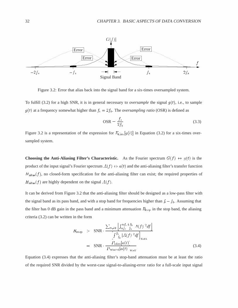
32 CHAPTER 3. BASIC ASPECTS OF DATA CONVERSION
�2fs �fs 2fsfs
Error
Error Error
Error
jG(f)j
f
Signal Band
Figure 3.2: Error that alias back into the signal band for a six-times oversampled system.
To fulfill (3.2) for a high SNR, it is in general necessary to oversample the signal g(t), i.e., to sample
g(t) at a frequency somewhat higher than fs = 2fb. The oversampling ratio (OSR) is defined as
OSR =fs2fb
(3.3)
Figure 3.2 is a representation of the expression for Ealias[g(t)] in Equation (3.2) for a six-times over-
sampled system.
Choosing the Anti-Aliasing Filter’s Characteristic. As the Fourier spectrum G(f) $ g(t) is the
product of the input signal’s Fourier spectrum A(f)$ a(t) and the anti-aliasing filter’s transfer function
Halias(f), no closed-form specification for the anti-aliasing filter can exist; the required properties of
Halias(f) are highly dependent on the signal A(f).
It can be derived from Figure 3.2 that the anti-aliasing filter should be designed as a low-pass filter with
the signal band as its pass band, and with a stop band for frequencies higher than fs�fb. Assuming that
the filter has 0 dB gain in the pass band and a minimum attenuation Rstop in the stop band, the aliasing
criteria (3.2) can be written in the form
Rstop > SNR �P
n6=0
hR nfs+fbnfs�fb
jA(f)j2dfi
hR fb�fb
jA(f)j2dfimax
= SNR � Palias[a(t)]
[Pinband[a(t)]]max
(3.4)
Equation (3.4) expresses that the anti-aliasing filter’s stop-band attenuation must be at least the ratio
of the required SNR divided by the worst-case signal-to-aliasing-error ratio for a full-scale input signal
3.1. FUNDAMENTAL STEPS IN A/D CONVERSION 33
a(t).
Unfortunately, (3.4) does not provide an absolute design criteria because whereas the full-scale signal-
band power [Pinband[a(t)]]max is usually well-specified, the worst-case power of the spectral components
that may alias back into the signal band is not. Hence, the specification of the the anti-aliasing filter can
only be based on a (qualified) assumption.
For low values of OSR, the ratio Palias[a(t)]= [Pinband[a(t)]]max should probably be estimated as at least
�40 dB, which may even be too optimistic. However, using this estimate in the specification for a high-
performance application with a required SNR of (say) 100 dB, it follows that the anti-aliasing filter must
have a stop-band attenuation of at least 60 dB.
It is well understood that, for relaxed pass-band requirements, the complexity of continuous-time low-
pass filters depends largely on the required stop-band attenuation2 and the relative width of the transition
band
fs � fbfb
=fsfb� 1 = 2OSR� 1 (3.5)
To obtain 60 dB stop-band suppression with a reasonably simple (say, third-order) filter, the OSR must
be at least 4 to 5.
It is important to notice that the above observation on the required OSR is general, and that it is not a
consequence of a particular choice of quantizer. Hence, quantizer structures that require a similar degree
of oversampling to operate, such as those proposed in this work, do not have strict limitations for their
applicability.
3.1.2 Errors Caused by the Sample-and-Hold Circuit
The S/H circuit performs the sampling of the signal, and thus it inflicts aliasing errors. These errors were
discussed in detail in the previous section 3.1.1.
2Relative to the pass-band gain.
34 CHAPTER 3. BASIC ASPECTS OF DATA CONVERSION
As any other analog circuit, the S/H circuit will cause errors such as noise, offset, and nonlinearity. In
particular, the sampling switch is a very critical design aspect, as it will cause charge injection, clock
feedthrough, and nonlinearity. Details on these aspects can be found in [27–32].
The S/H circuit must meet the overall design specification, so it is difficult to design for high-performance
applications. This work, however, does not address this design aspect.
Clock Jitter. All sampling circuits will be subject to clock-jitter problems. Jitter means that the signal
is sampled at slightly incorrect time instances (3.6)
gjitter(k) = g(kTs +�T (kTs)) (3.6)
where, for simplicity, it is assumed that j�T (t)j � Ts.
The simplification implies that jitter can modeled as a distortion of g(t) prior to the sampling instance.
More precisely, gjitter(k) is considered to be generated by sampling gjitter(t), which is a distorted repre-
sentation of g(t)
gh(k) = gjitter(kTs) = g(kTs) + gerror(kTs) (3.7)
where
gerror(kTs) ' �T (kTs)d
dt(g(kTs)) (3.8)
A model for the jitter-induced error is shown in Figure 3.3.
A low-jitter clock signal can be generated using a crystal-based oscillator. As this work focuses on the
baseband as the signal band, the magnitude of the first-order derivative dg(t)=dt will be moderate, and
gerror(t) will have a comparably low power. Hence, clock jitter is not considered to be a major problem
in this context. However, for band-pass applications (where dg(t)=dt may be large), clock-jitter errors
from the sampling process are of great concern. This aspect is discussed in more detail in Section 3.2.3.
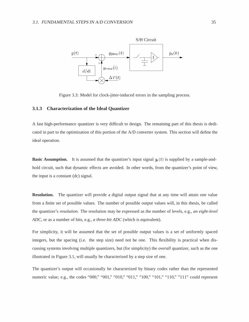
3.1. FUNDAMENTAL STEPS IN A/D CONVERSION 35
1
S/H Circuit
�T (t)
g(t) gjitter(t) gh(k)
d=dtgerror(t)
Figure 3.3: Model for clock-jitter-induced errors in the sampling process.
3.1.3 Characterization of the Ideal Quantizer
A fast high-performance quantizer is very difficult to design. The remaining part of this thesis is dedi-
cated in part to the optimization of this portion of the A/D converter system. This section will define the
ideal operation.
Basic Assumption. It is assumed that the quantizer’s input signal gh(t) is supplied by a sample-and-
hold circuit, such that dynamic effects are avoided. In other words, from the quantizer’s point of view,
the input is a constant (dc) signal.
Resolution. The quantizer will provide a digital output signal that at any time will attain one value
from a finite set of possible values. The number of possible output values will, in this thesis, be called
the quantizer’s resolution. The resolution may be expressed as the number of levels, e.g., an eight-level
ADC, or as a number of bits, e.g., a three-bit ADC (which is equivalent).
For simplicity, it will be assumed that the set of possible output values is a set of uniformly spaced
integers, but the spacing (i.e. the step size) need not be one. This flexibility is practical when dis-
cussing systems involving multiple quantizers, but (for simplicity) the overall quantizer, such as the one
illustrated in Figure 3.1, will usually be characterized by a step size of one.
The quantizer’s output will occasionally be characterized by binary codes rather than the represented
numeric value; e.g., the codes “000,” “001,” “010,” “011,” “100,” “101,” “110,” ”111” could represent

36 CHAPTER 3. BASIC ASPECTS OF DATA CONVERSION
the eight possible states of a 3-bit ADC. Whenever necessary for clarity, the step size will be identified
with the code as “101@8,” i.e., code “five” with a step size of eight. Similarly, a 3-bit@8 ADC means a
3-bit ADC with a step size of eight. All ADCs will have a minimum and a maximum code.
000
�
d(k): AssignedInteger Value
8
24
40
Gain = �1 LSB
�8
011
010
001
100
101
110
111
g(k): Analog Input
d(k): AssignedInteger Value
Output Codes
16
32
48
Offset
g(k): Analog Input
111
000
110
101
001
0101 LSB
Figure 3.4: Linear 3-bit@8 quantizers. Left: Definition of the step size (�) and of 1 LSB. Right:
Definition of offset and gain.
Ideal Operation. Figure 3.4 shows two linear 3-bit@8 quantizers. The quantizer shown to the left is
a proportional quantizer, which (except for the truncation) exhibits proportionality between the analog
input and the digital output (i.e., the assigned integer values). Notice that the unit “1 LSB” is defined
as an analog quantity, namely the variation of the analog input that will force a transition between two
neighbor output codes.
Although it is not a proportional quantizer, the quantizer shown to the right is also considered to be
linear. It illustrates that the assigned integer values can be chosen from any set of uniformly spaced
integers, for example, as shown f�8; 0; 8; 16; 24; 32; 40; 48g.
The quantizer’s gain is defined as the step size divided by 1 LSB. The quantizer’s offset is defined as the
analog value added to the analog input before it becomes a proportional quantizer; the shown quantizer
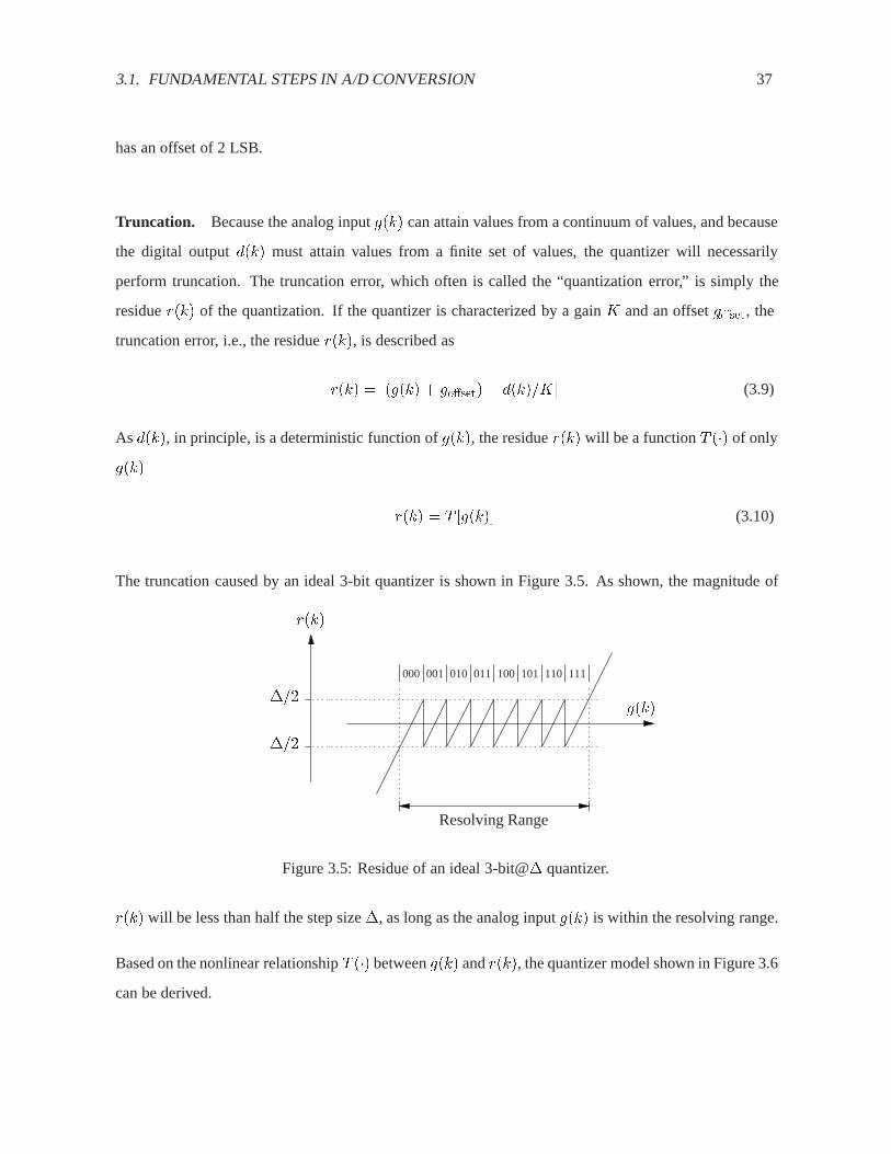
3.1. FUNDAMENTAL STEPS IN A/D CONVERSION 37
has an offset of 2 LSB.
Truncation. Because the analog input g(k) can attain values from a continuum of values, and because
the digital output d(k) must attain values from a finite set of values, the quantizer will necessarily
perform truncation. The truncation error, which often is called the “quantization error,” is simply the
residue r(k) of the quantization. If the quantizer is characterized by a gain K and an offset go�set, the
truncation error, i.e., the residue r(k), is described as
r(k) = [(g(k) + go�set)� d(k)=K] (3.9)
As d(k), in principle, is a deterministic function of g(k), the residue r(k) will be a function T (�) of only
g(k)
r(k) = T [g(k)] (3.10)
The truncation caused by an ideal 3-bit quantizer is shown in Figure 3.5. As shown, the magnitude of
r(k)
g(k)�=2
��=2
000 001 010 011 100 101 110 111
Resolving Range
Figure 3.5: Residue of an ideal 3-bit@� quantizer.
r(k) will be less than half the step size �, as long as the analog input g(k) is within the resolving range.
Based on the nonlinear relationship T (�) between g(k) and r(k), the quantizer model shown in Figure 3.6
can be derived.
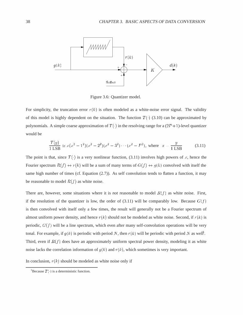
38 CHAPTER 3. BASIC ASPECTS OF DATA CONVERSION
r(k)
g(k) d(k)K
go�set
Figure 3.6: Quantizer model.
For simplicity, the truncation error r(k) is often modeled as a white-noise error signal. The validity
of this model is highly dependent on the situation. The function T (�) (3.10) can be approximated by
polynomials. A simple coarse approximation of T (�) in the resolving range for a (2P+1)-level quantizer
would be
T (y)
1 LSB' x(x2 � 12)(x2 � 22)(x2 � 32) � � � (x2 � P 2); where x =
y
1 LSB(3.11)
The point is that, since T (�) is a very nonlinear function, (3.11) involves high powers of x, hence the
Fourier spectrum R(f)$ r(k) will be a sum of many terms of G(f)$ g(k) convolved with itself the
same high number of times (cf. Equation (2.7)). As self convolution tends to flatten a function, it may
be reasonable to model R(f) as white noise.
There are, however, some situations where it is not reasonable to model R(f) as white noise. First,
if the resolution of the quantizer is low, the order of (3.11) will be comparably low. Because G(f)
is then convolved with itself only a few times, the result will generally not be a Fourier spectrum of
almost uniform power density, and hence r(k) should not be modeled as white noise. Second, if r(k) is
periodic, G(f) will be a line spectrum, which even after many self-convolution operations will be very
tonal. For example, if g(k) is periodic with period N , then r(k) will be periodic with period N as well3.
Third, even if R(f) does have an approximately uniform spectral power density, modeling it as white
noise lacks the correlation information of g(k) and r(k), which sometimes is very important.
In conclusion, r(k) should be modeled as white noise only if
3Because T (�) is a deterministic function.

3.1. FUNDAMENTAL STEPS IN A/D CONVERSION 39
(N � 2)�
L(3)
L(2)
L(1)
L(N � 3)
L(N � 2)
L(N � 1)
(N � 2)LSB
MissingCode
0
1
2
3
N � 3
N � 2
N � 1
Code #
ReferencePoint
ReferencePoint
Analog Input
LinearCharacteristic
Figure 3.7: Characteristic of a N-level nonideal quantizer with step size �.
� the properties of the correlation of g(k) and r(k) are not important,
� the quantizer has a high resolution (and many levels are excited), and
� the input g(k) includes substantial broad-band spectral components.
3.1.4 Characterization of Quantizer Errors
Very accurate quantizers are hard to realize. The spacing of the assigned integer values will (obviously)
be ideal, but the accuracy of their relation to the analog signal is prone to errors. Figure 3.7 shows the
static characteristic for an N-level nonideal quantizer with step size �. This section will classify the
various deviations from the ideal operation in terms of some well-known measures.
Linear Errors. It is not always obvious how a quantizer’s gain and offset should be defined. In fact,
the correct definitions often depend on the application.
For example, consider a system that requires a quantizer with an absolute specification on its gain and
offset. Since the specification is absolute, there is no need to distinguish between linear and nonlinear

40 CHAPTER 3. BASIC ASPECTS OF DATA CONVERSION
errors. Instead, the specification can be used as the reference, with respect to which all deviations are
considered to be errors. Errors can then be defined by (3.9) and modeled as shown in Figure 3.6.
Quite often, however, offset and gain errors are of little importance compared to the quantizer’s linearity.
In that case, it sometimes makes sense to define a best linear characteristic, with respect to which
nonlinear errors (including truncation) are defined. The problem is that the best linear characteristic may
be highly dependent on the analog input signal. Consider the quantizer shown in Figure 3.7. If the input,
for example, is such that only codes 2 and 3 are used, then the best linear characteristic would have a
higher gain and a different offset than the best linear characteristic for a signal where all codes are used.
To avoid inconsistency, the linear characteristic will be defined uniquely. For any N-level quantizer,
where N is greater than 2, there will be an maximum input value, L(1), for which all lower values will
be quantized to the minimum code. Similarly, there will be a minimum input value, L(N � 1), for
which all higher values will be converted to the maximum code. The linear characteristic is defined with
respect to the two reference points shown in Figure 3.7.
Accordingly, the unit 1 LSB is defined as
1 LSB =L(N � 1)� L(1)
N � 2(3.12)
and the quantizer’s gain K is defined as
K =�
1 LSB=
(N � 2)�
L(N � 1)� L(1)(3.13)
The offset is also defined with respect to the defined linear characteristic.
Nonlinear Errors. Truncation and other nonlinear errors are defined with respect to the defined linear
characteristic. For an N-level quantizer, an (N � 1)-element vector L(n) is defined. The nth element in
L(n) represents the lowest analog input4, for which code n occurs (see Figure 3.7).
Ideally, L(n) will consist of (N � 1) uniformly-spaced analog values. To characterize deviations from
the ideal behavior, two measures are defined with respect to L(n): the differential nonlinearity, DNL(n),
and the integral nonlinearity, INL(n).
4With the exception of L(N � 1), which is defined as previously described.
3.1. FUNDAMENTAL STEPS IN A/D CONVERSION 41
Each horizontal step of the quantizer’s characteristic should be 1 LSB wide. DNL(n) is a (N � 2)-
element vector representing each step’s deviation from the ideal width
DNL(n) = [L(n+ 1)� L(n)]� 1 LSB (3.14)
The transitions (marked with black dots in Figure 3.7) should occur at input values uniformly spaced
between L(1) and L(N � 1). The INL(n) is a (N � 1)-element vector representing the transitions’
deviation from the ideal locations
INL(n) = [L(n)� L(1)]� (n� 1) LSB
=
�L(n)� L(1)
L(N � 1)� L(1)� n� 1
N � 2
�(N � 2) LSB (3.15)
Notice that (by definition)
INL(1) = INL(N � 1) = 0 (3.16)
Often a quantizer is characterized by the largest elements of the two measures
INL = maxnjINL(n)j and DNL = max
njDNL(n)j (3.17)
A quantizer’s DNL and INL performance are typically expressed in LSBs. A quantizer described by a
good DNL has a smooth characteristic5 , but the overall linearity, i.e., the INL, need not be comparably
good [24]. On the other hand, a good INL implies a good DNL, because
DNL(n) = INL(n+ 1)� INL(n) (3.18)
Effective Number of Bits. It should be understood that a quantizer can be very linear without having
a high resolution, and also that a quantizer can have a high resolution without being very linear. It may
be relatively simple to increase a quantizer’s resolution, whereas it is almost always hard to increase its
relative linearity. In many publications, the relative linearity of data converters is expressed in terms of
a number of bits.
5Good local linearity.
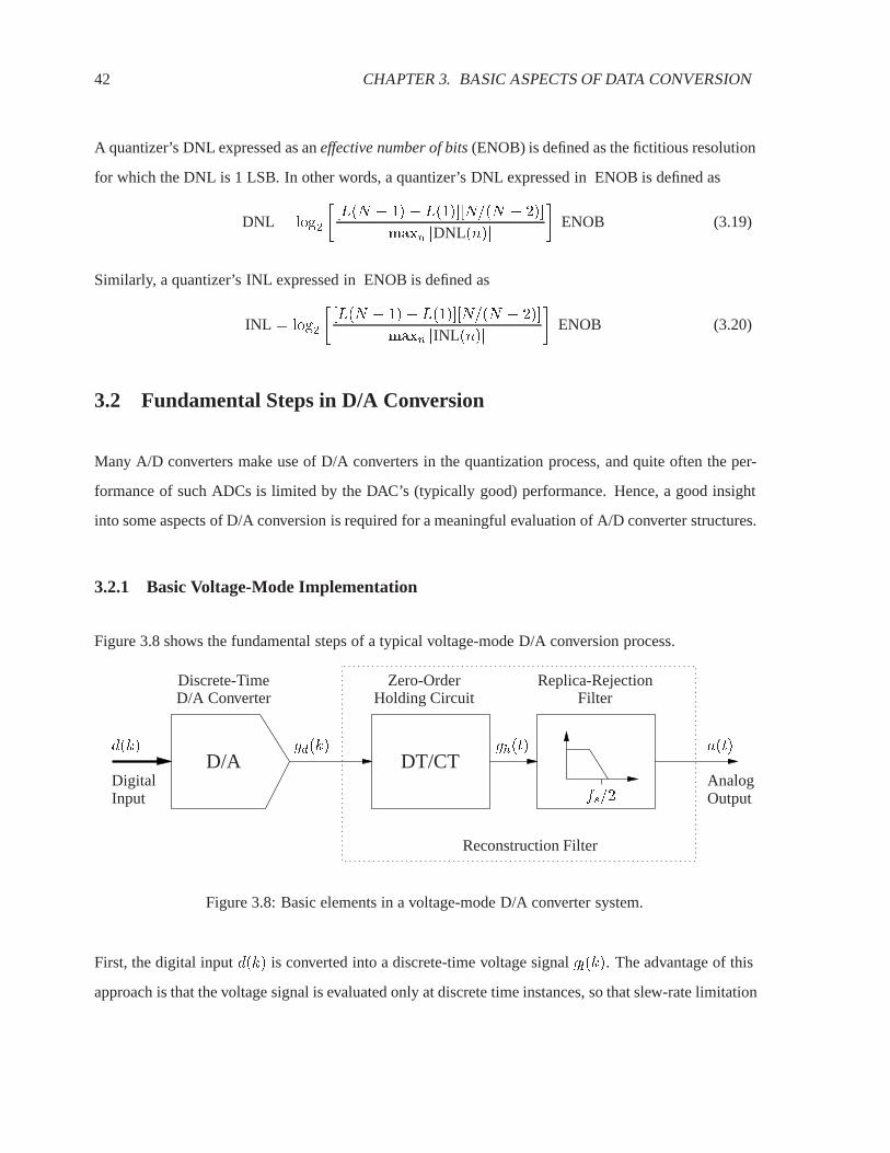
42 CHAPTER 3. BASIC ASPECTS OF DATA CONVERSION
A quantizer’s DNL expressed as an effective number of bits (ENOB) is defined as the fictitious resolution
for which the DNL is 1 LSB. In other words, a quantizer’s DNL expressed in ENOB is defined as
DNL = log2
�[L(N � 1)� L(1)][N=(N � 2)]
maxn jDNL(n)j�
ENOB (3.19)
Similarly, a quantizer’s INL expressed in ENOB is defined as
INL = log2
�[L(N � 1)� L(1)][N=(N � 2)]
maxn jINL(n)j�
ENOB (3.20)
3.2 Fundamental Steps in D/A Conversion
Many A/D converters make use of D/A converters in the quantization process, and quite often the per-
formance of such ADCs is limited by the DAC’s (typically good) performance. Hence, a good insight
into some aspects of D/A conversion is required for a meaningful evaluation of A/D converter structures.
3.2.1 Basic Voltage-Mode Implementation
Figure 3.8 shows the fundamental steps of a typical voltage-mode D/A conversion process.
D/Agd(k)
DigitalInput
d(k)
Discrete-TimeD/A Converter
DT/CTgh(t)
fs=2
Replica-RejectionFilter
Zero-OrderHolding Circuit
a(t)
AnalogOutput
Reconstruction Filter
Figure 3.8: Basic elements in a voltage-mode D/A converter system.
First, the digital input d(k) is converted into a discrete-time voltage signal gd(k). The advantage of this
approach is that the voltage signal is evaluated only at discrete time instances, so that slew-rate limitation

3.2. FUNDAMENTAL STEPS IN D/A CONVERSION 43
and other nonlinear settling effects of this circuit can be accepted. The discrete-time voltage signal gd(k)
is then DT/CT converted by a reconstruction filter.
The first stage of most reconstruction filters is a zero-order holding filter, which performs the DT/CT
conversion described by
gh(t) = gd(k) for kTs < t < (k + 1)Ts (3.21)
The circuit is, in principle, a S/H circuit, for which the output is evaluated in continuous time. The
operation can be modeled in the frequency domain as a filter with the transfer function6 (3.22) [33]:
HDT=CT(f) = Ts e�j�fTs
�sin(�fTs)
�fTs
�(3.22)
This filter will suppress the replica images (2.10) somewhat, but quite often, a dedicated replica-rejection
filter is needed to obtain further suppression.
Linearity of the Reconstruction Filter. The continuous-time evaluation of the output signal gh(t)
from the DT/CT converter is a very critical aspect. Ideally, gh(t) should be a staircase signal, but
this is impossible to obtain because it is not a continuous signal. Any implementation of a zero-order
holding circuit will include some degree of low-pass filtering, e.g., caused by the frequency response
of an employed op-amp. The main design aspect is, however, to make the circuit behave linearly. For
example, if the step size (i.e., the sample-to-sample variation) of gd(k) is large, the circuit is likely
to become slew-rate limited, resulting in a performance deterioration. An analysis will show that, to
preserve linearity, the discrete-time analog signal gd(k) should be oversampled at least ten times and
include only little out-of-band power.
Single-bit delta-sigma D/A converters represent the signal-band information in the form of a highly-
oversampled single-bit signal d(k). The advantage of this approach is that it may avoid nonlinearity in
the discrete-time D/A conversion process. However, because the analog equivalent is a rapidly-varying
two-level signal, it is nearly impossible to DT/CT convert it linearly. In the frequency domain, the
6Except for the phase shift factor e�j�fTs and the substitution of Tobs and Ts, the transfer function HDT=CT(f) is identical
to Wsq(f) defined as (2.15) and illustrated in Figure 2.3.

44 CHAPTER 3. BASIC ASPECTS OF DATA CONVERSION
problem can be detected as the signal having substantial power at frequencies outside the signal band.
To facilitate linear DT/CT conversion, the two-level voltage signal is typically filtered with a discrete-
time low-pass filter before it is DT/CT converted; see Figure 3.9 and [25].
fs=2 fs=2
D/A
Single-BitD/A Converter
d(k)
FilterSmoothening
DT/CT
Holding CircuitZero-Order Replica-Suppression
Filter
a(t)
0; 1; 1; 0; 1; 0; 1; 0; : : :
Figure 3.9: Output stage of a single-bit delta-sigma D/A converter.
Notice that the main purpose of the smoothing filter is to reduce the step size, and not in particular to
suppress the replica images (2.10). Whether it is necessary to suppress replica images more than by
the zero-order holding filter depends on the application. However, even if the application is indifferent
to the received signal’s spectral composition outside the signal band, the above discussion illustrates
that filtering may be necessary to avoid nonlinearity of the channel, which transmits the signal to the
application. Another example of this aspect could be a loudspeaker that distorts high-frequency energy,
thereby transforming it into signal-band energy that corrupts the signal detected by the human ear. In
this case, however, the long-term effects on the human ear’s sensitivity should also be considered.
Assuming that the step size somehow has been made sufficiently small, the DT/CT converter can be
implemented as shown in Figure 8 in [25].

3.2. FUNDAMENTAL STEPS IN D/A CONVERSION 45
3.2.2 Basic Current-Mode Implementation
Due to the absence of a simple high-performance current-mode sample-and-hold circuit for the im-
plementation of a zero-order holding circuit, current-mode DACs do usually not employ discrete-time
analog signals. Figure 3.10 shows a model of a current-mode D/A converter structure, where the usual
three-stage separation is indicated. It should, however, be understood that the separation is mainly theo-
retical, as it does not generally represent the implementation’s topology.
a(t)
AnalogOutput
D/Ad(k)
DigitalInput
Current-Mode DAC
D/A ConverterDiscrete-Time
gh(t)
fs=2
Continuous-Time
gd(k)DT/CT
Holding CircuitZero-Order
Replica-Rejection Filter
Figure 3.10: Current-mode D/A converter system.
Although other structures exist, such as R/2R and M/2M current splitters, the following will, without
loss of generality, assume that the current-mode DAC is implemented using the current-steering principle
shown in Figure 3.11. At the onset of each new sample, the array of switches is controlled according
to the input code d(k), thereby guiding the current from each element in the array of current sources to
either the output terminal or to a current-dump node at the same potential. The switches remain in the
same position until the onset of the next sample, therefore the output current will be a staircase current
signal. The output current is typically processed as a continuous-time signal, possibly by a continuous-
time replica-rejection filter.
Dynamic Errors. As discussed for voltage-mode D/A converters, the DT/CT conversion is a very
critical process. Assuming temporarily that the static linearity of the DAC is ideal, the focus will now be
on dynamic errors. Dynamic errors are caused by imperfect switching (glitches) when the output current
is updated from one value to the next.
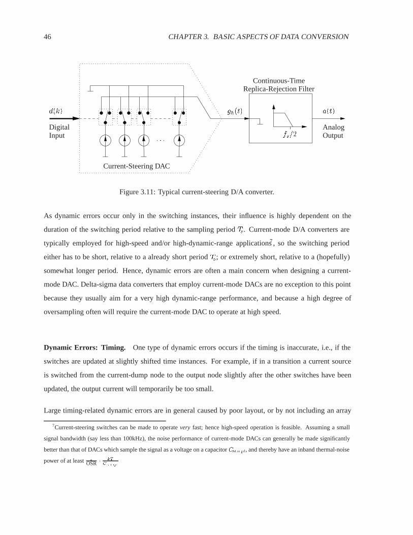
46 CHAPTER 3. BASIC ASPECTS OF DATA CONVERSION
fs=2
a(t)
AnalogOutput
d(k)
DigitalInput
gh(t)
� � �
Current-Steering DAC
Replica-Rejection FilterContinuous-Time
Figure 3.11: Typical current-steering D/A converter.
As dynamic errors occur only in the switching instances, their influence is highly dependent on the
duration of the switching period relative to the sampling period Ts. Current-mode D/A converters are
typically employed for high-speed and/or high-dynamic-range applications7, so the switching period
either has to be short, relative to a already short period Ts; or extremely short, relative to a (hopefully)
somewhat longer period. Hence, dynamic errors are often a main concern when designing a current-
mode DAC. Delta-sigma data converters that employ current-mode DACs are no exception to this point
because they usually aim for a very high dynamic-range performance, and because a high degree of
oversampling often will require the current-mode DAC to operate at high speed.
Dynamic Errors: Timing. One type of dynamic errors occurs if the timing is inaccurate, i.e., if the
switches are updated at slightly shifted time instances. For example, if in a transition a current source
is switched from the current-dump node to the output node slightly after the other switches have been
updated, the output current will temporarily be too small.
Large timing-related dynamic errors are in general caused by poor layout, or by not including an array
7Current-steering switches can be made to operate very fast; hence high-speed operation is feasible. Assuming a small
signal bandwidth (say less than 100kHz), the noise performance of current-mode DACs can generally be made significantly
better than that of DACs which sample the signal as a voltage on a capacitor Csampl, and thereby have an inband thermal-noise
power of at least 1
OSR � kTCsampl
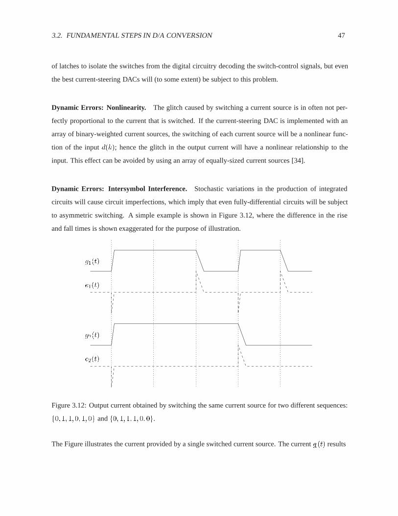
3.2. FUNDAMENTAL STEPS IN D/A CONVERSION 47
of latches to isolate the switches from the digital circuitry decoding the switch-control signals, but even
the best current-steering DACs will (to some extent) be subject to this problem.
Dynamic Errors: Nonlinearity. The glitch caused by switching a current source is in often not per-
fectly proportional to the current that is switched. If the current-steering DAC is implemented with an
array of binary-weighted current sources, the switching of each current source will be a nonlinear func-
tion of the input d(k); hence the glitch in the output current will have a nonlinear relationship to the
input. This effect can be avoided by using an array of equally-sized current sources [34].
Dynamic Errors: Intersymbol Interference. Stochastic variations in the production of integrated
circuits will cause circuit imperfections, which imply that even fully-differential circuits will be subject
to asymmetric switching. A simple example is shown in Figure 3.12, where the difference in the rise
and fall times is shown exaggerated for the purpose of illustration.
g1(t)
e1(t)
g2(t)
e2(t)
Figure 3.12: Output current obtained by switching the same current source for two different sequences:
f0; 1; 1; 0; 1; 0g and f0; 1; 1; 1; 0; 0g.
The Figure illustrates the current provided by a single switched current source. The current g1(t) results

48 CHAPTER 3. BASIC ASPECTS OF DATA CONVERSION
from a digital input d(k), where the corresponding switch is controlled by the sequence f0; 1; 1; 0; 1; 0g,
whereas g2(t) results from the sequence f0; 1; 1; 1; 0; 0g. The glitch currents e1(t) and e2(t) represent
for each of the two sequences the difference between the provided currents and the ideal two-level current
signals.
When the rise time and the fall time are identical, the glitch currents are proportional to the first-order
difference of the switching sequences, and hence the phenomenon can be made linear8. However, when
the switching is asymmetric, nonlinearity will result.
For simplicity, consider just the average value of the signals. The two switching sequences have the same
average value (one half), therefore linearity will require the two glitch currents to have the same average
value. However, due to asymmetric switching, the average value of each glitch current will instead be
linearly dependent on the number of rising and falling edges (cf. Figure 3.12). As g1(t) is switched more
often than g2(t), the two glitch currents do not have the same average value, consequently the system is
nonlinear. This effect is often referred to as intersymbol interference.
In order to avoid intersymbol interference, return-to-zero (RTZ) switching schemes have been intro-
duced [35] [36] [37]. The basic principle is that the switches of a current-steering DAC are controlled
according to the input d(k) only during the first fraction, say 3/4, of each period Ts, and according to
some fixed code in the remaining portion of each period. Figure 3.13 shows the output from the current
source when a RTZ switching scheme is employed for the two signal sequences that were considered
above. Notice that the average values of the two glitch currents, e1(t) and e2(t), are now the same. More
important, notice that the glitch current will always be proportional to the signal that is being converted
by the considered current source.
When using the RTZ switching scheme, the glitch current can be modeled simply as a small deviation
of the static value of the considered current source, and hence the technique is an efficient remedy for
dynamic errors caused by intersymbol interference. Phrased differently, the RTZ switching scheme
assures that the DT/CT conversion is described by an impulse response, which (by definition) assures
that the current source’s control signal (bit signal) is D/A converted linearly.
8For example, by employing only unit-sized current sources as discussed above.

3.2. FUNDAMENTAL STEPS IN D/A CONVERSION 49
g1(t)
e1(t)
g2(t)
e2(t)
Figure 3.13: Output of a current source when using the return-to-zero switching scheme.
3.2.3 Clock Jitter in D/A Converters
Clock jitter does usually not cause dominating errors because high-quality clock signals can be generated
using crystal-controlled clock generators. However, a D/A converter’s robustness to clock jitter is highly
dependent on the actual implementation, and for some high-performance DACs, clock-jitter-induced
errors can easily become dominating.
Modeling Clock Jitter Errors. D/A converters are sensitive to clock jitter only in the DT/CT con-
version process. Assuming at this point that the DT/CT converter is a zero-order holding circuit, the
jitter-distorted continuous-time output signal gjitter;h(t) can be described as
gjitter;h(t) = gd(k); for kTs +�T (k) � t < (k + 1)Ts +�T (k + 1) (3.23)
where, for simplicity, it has been assumed that �T (k); k 2 Z is a zero-mean stochastic process charac-
terized by a standard deviation much less than the sampling period Ts.
The jitter-induced error signal gjitter;error(t), i.e., the difference between gjitter;h(t) and the ideal output
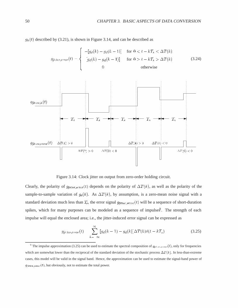
50 CHAPTER 3. BASIC ASPECTS OF DATA CONVERSION
gh(t) described by (3.21), is shown in Figure 3.14, and can be described as
gjitter;error(t) =
8>>><>>>:�[gd(k) � gd(k � 1)] for 0 < t� kTs < �T (k)
[gd(k)� gd(k � 1)] for 0 > t� kTs > �T (k)
0 otherwise
(3.24)
Ts Ts Ts Ts Ts
�T (2) > 0 �T (3) < 0
�T (4) > 0 �T (5) < 0
�T (6) < 0
gjitter;h(t)
�T (1) > 0gjitter;error(t)
Figure 3.14: Clock jitter on output from zero-order holding circuit.
Clearly, the polarity of gjitter;error(t) depends on the polarity of �T (k), as well as the polarity of the
sample-to-sample variation of gd(k). As �T (k), by assumption, is a zero-mean noise signal with a
standard deviation much less than Ts, the error signal gjitter;error(t) will be a sequence of short-duration
spikes, which for many purposes can be modeled as a sequence of impulses9. The strength of each
impulse will equal the enclosed area; i.e., the jitter-induced error signal can be expressed as
gjitter;error(t) =
1Xk=�1
[gd(k � 1)� gd(k)]�T (k)Æ(t � kTs) (3.25)
9 The impulse approximation (3.25) can be used to estimate the spectral composition of gjitter;error(t), only for frequencies
which are somewhat lower than the reciprocal of the standard deviation of the stochastic process �T (k). In less-than-extreme
cases, this model will be valid in the signal band. Hence, the approximation can be used to estimate the signal-band power of
gjitter;error(t), but obviously, not to estimate the total power.

3.2. FUNDAMENTAL STEPS IN D/A CONVERSION 51
Notice that gjitter;error(t) is the time-domain equivalent10 of
gjitter;error(k) = [gd(k � 1)� gd(k)]�T (k)
Ts(3.26)
and hence, the spectral composition of gjitter;error(t) can be found by convolving the Fourier spec-
trum of the first-order difference of �gd(k) with the Fourier spectrum of the relative-clock-jitter signal
�T (k)=Ts.
Clock jitter will include a flicker-noise component and a thermal-noise component. However, it is gen-
erally the jitter’s thermal-noise component that may cause problems, and hence the flicker-noise compo-
nent will be neglected in the following.
Given the assumption that �T (k)=Ts is a white-noise signal, i.e that it is a sequence of identically-
distributed independent stochastic events, it follows that gjitter;error(k) will be a signal with uniform
power density11. The total power of gjitter;error(k) will be the power of �T (k)=Ts multiplied by the
average step size of gd(k).
Without taking extreme measures and for a sampling frequency in the few-MHz range [38], the stochastic
element �T (k)=Ts can be made to have a standard deviation in the order of 50pS � 2MHz = 10�4. This
value will be used in the following evaluations to get a feeling of the problem’s significance.
Clock Jitter in Voltage-Mode D/A Converters. Voltage-mode D/A converters will typically employ a
zero-order holding circuit for the DT/CT conversion, and hence the above derivation will apply directly.
The worst-case12 average value of jgd(k � 1)� gd(k)j is �pp=OSR, where �pp is the full-scale peak-
to-peak signal swing.
Knowing that the clock-jitter-induced error signal gjitter;error(t) has a uniform spectral power density,
10As defined by (2.9).11Although gjitter;error(k) has uniform power density, it is not a white-noise signal. The individual samples are modulated
with [gd(k � 1)� gd(k)], so it is not a stationary stochastic process.12Assuming a full-scale signal at the highest signal-band frequency.

52 CHAPTER 3. BASIC ASPECTS OF DATA CONVERSION
the worst-case signal-band power can be calculated as
P [gjitter;error(t)] <\
��T (k)
Ts
�2� �pp
OSR
�2 1
OSR
' 10�8 � �2pp
OSR3 (3.27)
where\
��T (k)
Ts
�2 ' 10�8 represents the above assumption of a fair estimate for what can be achieved
without taking extreme measures, i.e. for what is considered to be a reasonable requirement for well-
designed mass-produced electronic equipment. As the full-scale signal power is �2pp=8, it follows that
the signal-to-noise ratio (SNR) will be in the order of 107OSR3. As discussed on page 43, voltage-mode
DACs will usually operate on at least ten times oversampled signals, in which case the SNR estimate
will be 100 dB.
The conclusion is that clock-jitter-induced errors typically can be made non-dominating in voltage-mode
DACs of up to 16-bits of resolution (audio quality). Notice, however, that this is not the case if the signal
is significantly less oversampled. It is quite difficult to meet the clock-jitter requirement for a 16-bit
DAC operating at Nyquist rate, i.e., for OSR = 1. In this case, the clock-jitter requirement is just
a few pS for a 2MHz clock signal – a level of performance which normally will require a stabilized
laboratory test setup. This is yet another reason for why high-performance DACs must operate on
somewhat oversampled signals.
Clock Jitter in Current-Mode D/A Converters. In principle, the clock-jitter sensitivity of current-
mode DACs is the same as that of voltage-mode DACs. In reality, however, the situation is often much
less favorable.
Consider a current-mode DAC, which is designed to meet the same specifications as those of a good
voltage-mode DAC. High-performance current-mode DACs are usually designed to operate with a RTZ
switching scheme in order to avoid intersymbol interference errors (cf. page 47). A problem arises
because the RTZ switching scheme produces a signal which (for each sample) has two clock-jitter-prone
edges instead of just one, and because the average step size (per sample) will be �pp independent of the
OSR. Hence, to meet the same specifications, the standard deviation of �T (k)=Ts must be a factor of
3.2. FUNDAMENTAL STEPS IN D/A CONVERSION 53
OSR smaller for the current-mode implementation than for the voltage-mode implementation. Because
the improved thermal noise performance often is the main incentive to implement a DAC in current
mode, the system specifications can be quite tough, therefore, the clock-jitter requirement can become
extreme (a requirement of less than 1 pS of clock-jitter is not uncommon, but it is extremely difficult to
fulfill).
In conclusion, the only way to avoid very strict clock-jitter requirements is to implement the current-
mode DAC without RTZ switching, in which case other techniques must be employed to avoid inter-
symbol-interference errors. Such alternative techniques are discussed in the second part of this thesis
and in [35].
3.2.4 Static Performance of D/A Converters
The fundamental requirement of any D/A converter is that it should generate an analog signal which is
proportional to the digital input. This section will define the DAC’s static characteristic, its gain and
offset, some terminology, and some measures for static DAC nonidealities.
Static Output Value. The static performance of a DAC is evaluated when the input is held constant.
The static analog output corresponding to a considered code is defined as the average value of the pro-
vided output.
Resolution and Step Size. The set of permitted digital input codes is assumed to represent a set of
integers, which are uniformly distributed with the step size �. The resolution is defined as the number
of permitted input codes. The notation, “3-bit@� DAC,” represents a DAC with eight permitted input
codes representing integers spaced with the step size �.
Static Characteristic. The static characteristic is defined as the relation between each represented
integer and the corresponding static analog output. The static characteristic of an N-level DAC can be
described by a vector S(n), where S(1) is the static analog output for the smallest represented integer,
and S(N) is the static analog output for the largest represented integer (see Figure 3.15).
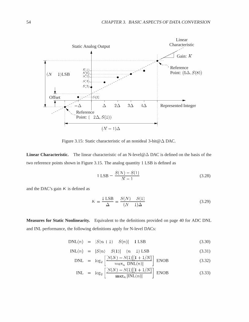
54 CHAPTER 3. BASIC ASPECTS OF DATA CONVERSION
CharacteristicLinear
Gain: K
ReferencePoint: (�2�; S(1))
(N � 1)�
� 2� 3� 4���
Static Analog Output
S(3)
S(4)
S(5)S(6)S(7)
Represented Integer
ReferencePoint: (5�; S(8))
S(2)Offset
(N � 1)LSB
Figure 3.15: Static characteristic of an nonideal 3-bit@� DAC.
Linear Characteristic. The linear characteristic of an N-level@� DAC is defined on the basis of the
two reference points shown in Figure 3.15. The analog quantity 1 LSB is defined as
1 LSB =S(N)� S(1)
N � 1(3.28)
and the DAC’s gain K is defined as
K =1 LSB�
=S(N)� S(1)
(N � 1)�(3.29)
Measures for Static Nonlinearity. Equivalent to the definitions provided on page 40 for ADC DNL
and INL performance, the following definitions apply for N-level DACs:
DNL(n) = [S(n+ 1)� S(n)]� 1 LSB (3.30)
INL(n) = [S(n)� S(1)]� (n� 1) LSB (3.31)
DNL = log2
�[S(N)� S(1)][1 + 1=N ]
maxn jDNL(n)j�
ENOB (3.32)
INL = log2
�[S(N)� S(1)][1 + 1=N ]
maxn jINL(n)j�
ENOB (3.33)

3.2. FUNDAMENTAL STEPS IN D/A CONVERSION 55
3.2.5 Linearity Limitations
This section will discuss the factors that limit a DAC’s static linearity. The discussion will only address
DACs that generate the analog output signal as a sum of one or more concurrent analog signals, such as,
for example, the current-steering DAC shown in Figure 3.11.
Basic Principle for D/A Conversion. The basic principle for many D/A converters is shown in Fig-
ure 3.16.
DAC
DAC
DAC
DAC
c0(k)
c1(k)
c2(k)
c3(k)
cP�1(k)DAC
d(k)
b0(k)
b1(k)
b2(k)
b3(k)
bP�1(k)
a(k)
Digital
Front-End
(Separator)
Figure 3.16: Topology of most D/A converters.
The digital front-end separates the digital input signal d(k) into a sum of P digital signals:
d(k) =
P�1Xi=0
bi(k) (3.34)
These P signals will in general be of low resolution, such that they are easy to D/A convert individually.
The P DACs all have the same nominal gain K , therefore the analog output a(k) can be formed simply
by adding the generated analog signals ci(k)
a(k) =
P�1Xi=0
ci(k) =
P�1Xi=0
Kbi(k) = Kd(k) (3.35)
56 CHAPTER 3. BASIC ASPECTS OF DATA CONVERSION
The digital front end can be implemented with arbitrary accuracy. Any nonideality of this type of D/A
converter must, therefore, originate from either the individual D/A conversions or from the summing
operation.
If the analog signals ci(k) are represented as currents, the summing operation can be implemented sim-
ply by connecting them to one common node (shown in Figure 3.11). Kirchoff’s current law assures that
the summation will be ideal for all practical purposes. However, because voltage signals are difficult
to add accurately, voltage-mode DACs are typically implemented as switched-capacitor (SC) circuits,
in which case the analog signals ci(k) are represented as charge pulses (which can be added as ideally
as currents). The issue of accurately summing ci(k) is thereby replaced by the problem of accurately
converting the discrete-time summed-charge signal into a discrete-time voltage signal. This design as-
pect is well understood, and circuits, the linearity of which is limited mainly by the linearity of the
available capacitors, are known [39]. Although highly dependent on the technology used, poly-to-poly,
metal-to-poly, and metal-to-metal capacitors will be up to 14-18 bits linear13.
The sum of the individual DACs’ offsets will be the overall DAC’s offset, but they will not cause any
other errors. As the offset of the overall DAC usually is not considered to be a critical parameter, offsets
in the individual DACs are of only little concern.
In conclusion, the static linearity of DACs, which are implemented in the topology shown in Figure 3.16,
is affected only by inaccurate gain and nonlinearities of the individual DACs.
Binary-Weighted D/A Converters. Usually, the digital input signal d(k) is coded in the binary format,
which makes binary-weighted DACs especially simple to implement. For such DACs, the digital front
end is just a simple separation, where b0(k) is the most-significant bit of d(k), b1(k) the second-most-
significant bit of d(k), etc.. Assuming that d(k) is of five-bit resolution, b0(k) will attain only two values:
0 and 16; also b1(k) will attain only two values: 0 and 8, etc.. Each of the five DACs will, therefore,
13The linearity of a capacitor/resistor is defined as the linearity of the exploited part of the function describing the charge-to-
voltage/voltage-to-current relationship. The DNL and INL linearity of a function f(x), in a range of values x 2 J , is defined
using the expressions (3.32) and (3.33). Here, S(n) = f(xn), where xn is a set of N ! 1 uniformly distributed values in
J . The text refers to the estimated INL linearity.
3.2. FUNDAMENTAL STEPS IN D/A CONVERSION 57
consist of only one analog source, which is turned on and off according to the corresponding signal
bi(k). As the input signals bi(k) are binary scaled, so will the analog sources constituting the five DACs
be binary scaled.
Now, consider the static linearity. Each of the five internal DACs is a two-level DAC, hence individually,
they are all inherently linear14. In other words, each of the separated signals bi(k) will be D/A converted
linearly, implying that only differences of the individual DACs’ gain may cause static nonlinearity. As-
sume that the nominally identical gains of the five DACs are K0, K1, K2, K3, and K4. The gain of the
overall DAC will, therefore, be
bK =16K0 + 8K1 + 4K2 + 2K3 + 1K4
16 + 8 + 4 + 2 + 1(3.36)
which leads to the following description of the output-referred nonlinearity error
aerror(k) = a(k)� bKd(k)� ao�set
=
4Xi=0
bi(k)(Ki � bK) (3.37)
Using Schwartz’s inequality, it follows that
jaerror(k)� aerror(k � 1)j �4X
i=0
jbi(k)� bi(k � 1)j(Ki � bK) (3.38)
As each of the separated signals bi(k) are related to d(k) by modulo functions, even small changes in
d(k) can result in large changes in bi(k), and consequently in large changes aerror(k). In other words,
binary-weighted DACs will typically exhibit a poor DNL performance, so they are not suitable for D/A
conversion of large-dynamic-range signals.
Unit-Element DACs. A DAC with a good DNL is preferable for D/A conversion of large-dynamic-
range signals. Unit-element DACs have this property.
Still referring to Figure 3.16, the digital front end of a N -bit@1 unit-element DAC separates the digital
input into (2N � 1) signals bi(k), which all attain only two values: 0 and 1. An array of (2N � 1)
14Because the static characteristic consists of only two points, which will always define a straight line.
58 CHAPTER 3. BASIC ASPECTS OF DATA CONVERSION
nominally-identical DACs, each consisting of only one analog source, is used to generate the analog
output a(k) by turning on as many of these analog sources as the digital input d(k) prescribes.
Assuming that the gains of the individual DACs are described by K0;K1; : : : ;K(2N�2), the overall
DAC’s gain bK will be
bK =
P2N�2i=0 Ki
2N � 1(3.39)
which leads to the following description of the output-referred nonlinear error
aerror(k) = a(k)� bKd(k)� ao�set
=2N�1Xi=0
bi(k)(Ki � bK) (3.40)
If, as usual, the digital front end is of the thermometer-coding type
bi(k) = 1 for i < d(k); and bi(k) = 0 otherwise (3.41)
it implies that a small variation in d(k) will cause a comparably small variation in aerror(k) because only
as many as jd(k) � d(k � 1)j terms are altered in the summation in (3.40).
More precisely, the DAC’s DNL is simply the maximum absolute deviation from the average value of the
analog sources. This will generally be 3-5 times the standard deviation of the individual analog source,
which for modern technologies is typically less than 0.01 LSB.
Sectored DACs. Clearly, because the digital front end and especially the interconnection of unit-
element DACs can easily become quite involved15, they are more difficult to implement than their
binary-weighted counterparts. Using the unit-element-DAC topology is often unnecessary, because a
simple analysis will show that the stochastic properties16 of the INL performance are the same as those
of a binary-weighted DAC, and because only few applications will require a DNL performance as good
15Unit-element DACs are, however, not as complicated to implement as they may appear at first sight. Some details on this
aspect can be found in [34].16The stochastic properties of the INL will typically only depend on the output value, which will be the same.

3.2. FUNDAMENTAL STEPS IN D/A CONVERSION 59
as 0.01 LSB. Sectored DACs represent a compromise between complexity and DNL performance [40].
In these converters, the least-significant bits are D/A converted with binary-weighted DACs, whereas the
most-significant bits are first thermometer coded and then D/A converted with unit-element DACs.
Matching of Analog Sources. The relative matching of electrical properties spatially distributed on an
integrated-circuit surface depends somewhat on the layout technique. Any on-chip electrical parameter
will usually be a function f(x; y) of the on-chip coordinates as well as subject to a stochastic variation.
For a given area A used for the implementation of supposedly matched devices, the variation of f(x; y)
over A will typically be larger than the stochastic process’ standard variation due to systematic errors
and gradients in processing. Hence, to obtain good matching, one should strive to cancel the effect of
f(x; y).
As f(x; y) is generally unknown, it has become common practice to cancel only the linear trend in
f(x; y) using the common-centroid layout principle, i.e., to lay out each matched element on an area
Ai � A, such that the centroid (xcc; ycc) is the same for all elements
(xcc; ycc) =
�ZZAi
x dxdy;
ZZAi
y dxdy;
�(3.42)
Obviously, the common-centroid layout technique will provide the best cancellation when the matched
devices are laid out on a small area A. However, to assure a small standard deviation of the matching
process’ stochastic element, the matched devices should preferably be large. These two requirements
are not necessarily contradictory because each device in a set of matched devices can be implemented
as a parallel combination of several small devices, each small device being a matched element in one of
several arrays of matched devices, each array being implemented in a small area.
In principle, arbitrarily good matching can be obtained using the above technique, but in reality, con-
siderations such as chip area (cost), yield, power consumption, dynamic effects and/or stray capacitance
will limit the obtainable relative matching.
Conclusion. The static linearity of the discussed types of DACs is singularly dependent on the relative
accuracy with which an array of analog sources can be implemented. Whereas the DNL performance

60 CHAPTER 3. BASIC ASPECTS OF DATA CONVERSION
can be made almost arbitrarily good by using a (partly) thermometer-coding digital front end, the INL
performance can only be improved by improving the relative matching of the analog sources. When
using a modern technology and good layout techniques, the INL performance can be made as good
as 10–12 bits. Laser trimming and other once-and-for-all post-processing calibration techniques can
be used to obtain better matching, but they are expensive to perform and they lack the ability to track
effects due to, for example, aging and temperature. Better alternatives include power-up and background
calibration, but these techniques tend to require a relatively large chip area for their implementation, and
they are subject to leakage effects if the compensation parameter is stored in analog form on a capacitor.
3.3 Measuring Dynamic Performance
Unless a data converter is used for ultra-low-bandwidth applications, its linearity may not be fully de-
scribed by its static performance measures, i.e., its DNL and INL description. For high-speed data
conversion, it is the dynamic performance rather than the static performance which is of interest.
Several factors may limit the dynamic performance. Examples include nonlinearities of the filters, S/H
circuits, and DT/CT converters used; clock-jitter effects; device noise and noise coupling; etc.. Be-
cause static nonlinearity also will manifest itself as dynamic nonlinearity, a thorough description of a
converter’s dynamic performance avoids the need for a static linearity description.
The dynamic performance is best described in the frequency domain. The data converter is operated
under certain test conditions, and the performance is evaluated as the output-referred ratio of the applied
signal’s power relative to the power of the considered error. To ease the process of separating the output
signal’s power in terms of “signal” and “error,” the applied test signal will typically consist of one or
more sinusoids.
As the dynamic performance may depend significantly on the test conditions, the measurements should
be repeated for many sets of test conditions, and the results presented in a graphical format. Obviously,
full particulars of the measurement technique and test conditions used are an essential part of the results.

3.3. MEASURING DYNAMIC PERFORMANCE 61
3.3.1 Signal-to-Noise Ratio
Noise is the term often used to indicate those errors for which the source is assumed to be of stochastic
nature. Because noise in general will have to be considered in its wide sense, it need not be independent
of the input signal. Noise sources include thermal and flicker device noise, substrate- and capacitively-
coupled noise, clock-jitter-induced noise, and quantization noise.
The signal-to-noise ratio (SNR) is usually measured for a sinusoid input signal and plotted as a function
of the input signal’s amplitude. Harmonic distortion and other errors, which are described by separate
measures, are not included in the estimated error power17.
If the noise power is signal-independent, which is the case for device noise, the SNR will be linearly
dependent on the input signal’s magnitude. If the SNR saturates a given level, it indicates that clock-
jitter-induced noise dominates from that level and up. For single-bit delta-sigma modulators, the SNR
will not only saturate but drop for input signals above a certain level. This occurs when the internal
one-bit quantizer becomes overloaded, in which case the quantization-noise power increases faster than
the signal power.
The signal-band noise power is calculated by integration of the estimated spectral power density over
the signal band, hence a wide-bandwidth application will be relatively more sensitive to noise than a
narrow-bandwidth application18. The lower limit (in frequency) of flicker noise is a somewhat tricky
issue, but it is not important for the following discussion.
3.3.2 Dynamic Range
The dynamic range (DR) is defined on basis of the SNR. The DR is the ratio of the magnitude of
the largest sinusoid input that does not cause clipping or other coarse nonlinear effects, relative to the
magnitude of the sinusoid input for which the SNR is 0 dB.
17The signal-to-noise-and-distortion ratio (SNDR) is a composite measure, for which the error consist of all signal-band
spectral components which are not in linear relation to the applied input signal.18Also, as the total signal-band power of the sampling thermal noise (kT/C noise) in switched-capacitor circuits is inversely
proportional to both the capacitor size and the oversampling ratio, large capacitors are required for SC circuits with low OSR.

62 CHAPTER 3. BASIC ASPECTS OF DATA CONVERSION
3.3.3 Spurious-Free Dynamic Range
A full-scale sinusoid of frequency f0 is applied as test input, and the output signal is evaluated at all
frequencies in the signal band. The ratio of the estimated power density of the output signal’s spectral
component centered at f0 and the largest other spectral component is called the spurious-free dynamic
range (SFDR). Often, the SFDR is close to the reciprocal of the total harmonic distortion (THD), but in
some implementations the largest spurious spectral component occurs at a frequency which is not in a
harmonic relationship to f0.
3.3.4 Intermodulation Distortion
Simple harmonic-distortion measurements are not suitable to evaluate high-frequency linearity. The
problem is that the dominating harmonic may occur at a frequency outside the signal band, therefore,
if out-of-band spectral components are rejected, for example, by low-pass filtering, the measurement
may provide misleadingly optimistic results. To avoid this scenario, the linearity should be evaluated
as a signal-to-distortion ratio where the distortion is the intermodulation product occurring in the signal
band.
3.4 Quantizer Topologies
Again addressing the implementation of A/D converters, this section will provide an overview of some
commonly used quantizer topologies. Each topology is associated with advantages and disadvantages in
terms of linearity, speed, power consumption, complexity, and latency.
Although quantizers can be classified in several ways, the following will consider quantizers to be sep-
arated into two main categories: data quantizers and signal quantizers. A data quantizer is defined as
a quantizer that evaluates each input sample as accurately as possible, and which does not take any
sample-to-sample correlation into account. In other words, a data quantizer’s output approximates the
time-domain description of the received signal (cf. Section 2.1). A signal quantizer, on the other hand,

3.4. QUANTIZER TOPOLOGIES 63
is defined as a quantizer that evaluates the input signal’s spectral composition as accurately as possible.
Each sample may or may not be quantized accurately, but the quantizer has memory and it assures that
the sequence of errors, i.e., the error signal, has very little energy in the signal band. In other words, a
signal quantizer approximates the signal-band frequency-domain description of the received signal (cf.
Section 2.2).
Because the Fourier transformation is a bijective19 relation between the time domain and the frequency
domain, an ideal data quantizer will yield exactly the same output signal as an ideal signal quantizer. The
difference will show only in the presence of quantizer nonidealities, where a data quantizer can produce a
substantial amount of signal-band quantization noise and harmonic distortion, whereas a signal quantizer
will suppress such errors in the signal band by moving the energy to other frequencies outside the signal
band. Clearly, a signal quantizer will require a minimum degree of oversampling. Elsewhere, they are
sometimes referred to as oversampling quantizers.
It is the application that determines which type of quantizer should be used. For example, if the appli-
cation is to measure the resistance of a large number of produced resistors to facilitate estimation of the
production’s standard deviation, the resistance of each resistor represents data which should be evaluated
using a data quantizer and not a signal quantizer. However, the majority of applications process signals
rather than data; in such cases a signal quantizer may be the better choice.
3.4.1 Direct-Comparison Data Quantizers
Data quantizers will be classified as one of two types, one of which is called Direct-Comparison quan-
tizers. Direct-Comparison quantizers are all characterized by the property that the (possibly sampled-
and-held) input signal is quantized by multiple comparisons with analog signals generated by D/A con-
version.
19I.e. there is a one-to-one correspondence.
64 CHAPTER 3. BASIC ASPECTS OF DATA CONVERSION
Counting Quantizers. Extremely good linearity20 can be obtained using quantizers of the counting
type, such as dual-slope and incremental [41] quantizers, but the achievable bandwidth is so low that
they are useful mainly for instrumentation and calibration purposes, which nonetheless are important
applications for data converters.
Successive-Approximation Quantizers. Higher bandwidth and good resolution can be obtained using
successive-approximation quantizers, where each input sample is digitized by generating a sequence
of successively improved approximations. Each approximation is D/A converted, and the output is
compared with the sampled-and-held input. The result of each comparison is used as the basis for the
next supposedly-improved approximation.
In principle, the uncertainty of each new approximation in the sequence of approximations is reduced
by a factor of two21, but (obviously) the uncertainty of any approximation cannot be reduced to less
than the uncertainty by which the approximation is D/A converted, that is, the employed DAC’s INL
performance. In other words, the linearity of a successive-approximation quantizer is limited by the
linearity of the employed DAC, which typically will be in the order of 10 bit. Assuming that only 1 bit is
resolved for each new approximation, ten cycles will be necessary to resolve an input sample for 10-bit
conversion, which, combined with a minimum degree of oversampling22 (see section 3.1.1), will limit
the bandwidth to less than one percent of the cycle frequency, i.e. , typically well below 1MHz.
Flash Quantizers. Flash quantizers are among the fastest quantizers available. By means of (for ex-
ample) a resistor string, N supposedly equidistant analog reference signals (say voltages) are generated.
At the sampling instances, the input signal is simultaneously compared to each and all of these N refer-
ence signals, thereby producing N one-bit digital signals, which jointly represent the quantized value in
the thermometer-coded format. A digital back end is in general used to recode the digital signal into the
20In excess of 20 bits.21This is the typical case, but more than one bit can be resolved in each cycle.22This, of course, only makes sense if the quantizer is used for a signal-quantizer application.

3.4. QUANTIZER TOPOLOGIES 65
more dense binary-coded format23.
As N comparators are required for the implementation of an N -level quantizer, flash quantizers typi-
cally have a fairly low resolution, say less than 8 bits. The main sources of nonlinearity include non-
equidistant spacing of the generated analog signals (DAC nonlinearity) and the offsets of the individual
comparators. Interpolation techniques can, however, be used efficiently to reduce the offset-induced
nonlinearity. Depending on the actual implementation24, the INL performance is typically in the order
of 5–10 bits.
Flash quantizers can be designed for high-speed quantization. Sampling frequencies well beyond 100
MHz are achievable, but their main limitations are high circuit complexity and power consumption, low
resolution, and somewhat poor linearity.
Subranging Quantizers. Subranging quantizers represent a compromise between conversion speed
and circuit complexity. The sampled-and-held input signal is first compared to N voltages equidistantly
spaced in the full range, whereafter the same N comparators are used to compare the input signal with
N voltages equidistant spaced in a smaller range centered around the voltage estimated in the first
quantization. In this way, an N2-level quantizer can be implemented using only N comparators. These
quantizers can be designed to have an INL linearity in the order of 8–10 bits, and they are often employed
in portable video equipment.
3.4.2 Residue-Calculating Data Quantizers
The second type of data quantizers is called Residue-Calculating quantizers. They are, in principle,
all based on the simple residue-calculating stage shown in Figure 3.17. The stage’s input signal g(t)
is quantized by a (typically flash-type direct-comparison) quantizer providing the digital output signal
d(k). The signal d(k) is D/A converted and the result is subtracted from the stage’s input signal g(t) to
23The digital back end may also include some logic to prevent the deleterious effects from “bubbles” in the thermometer
codes.24Although it may seem unnecessary, a good S/H circuit is often required to obtain good linearity.

66 CHAPTER 3. BASIC ASPECTS OF DATA CONVERSION
produce br(k). This operation can be described as
g(k) = br(k) + d(k)KDAC +ODAC + INLDAC[d(k)] (3.43)
where KDAC is the DAC’s gain, ODAC is the DAC’s offset, and INLDAC[d(k)] represents the DAC’s
INL error for the codes representing d(k). Notice that br(k) is an estimate of the residue r(k) of the
quantization d(k) of g(k) calculated with respect to the linear characteristic defined by the DAC (cf.
Equation (3.9) where go�set = �ODAC and K = 1=KDAC).
g(k)
br(k) d(k)
Figure 3.17: Basic residue stage used in most residue-calculating quantizers.
The overall point is that, if br(k) is quantized by a quantizer with gain K1 = 1=KDAC, so that d1(k) =br(k)=KDAC, it follows from (3.43) that
g(k) = d1(k)KDAC + d(k)KDAC +ODAC + INLDAC[d(k)]
= [d1(k) + d(k)]KDAC +ODAC + INLDAC[d(k)] (3.44)
Equation (3.44) implies that, given the above assumption, the linear characteristic and the nonlinearity
of the quantizer, evaluated from g(k) to [d(k) + d1(k)], are defined only by the employed DAC. Thus, a
residue-calculating quantizer can, in principle, be implemented with the same linearity as that of a DAC.
Obviously, it is preferable to match the quantizer’s linear characteristic to the DAC’s linear charac-
teristic25, in which case jbr(k)j < 0:5 LSBDAC, but this is actually not a strict requirement, because
mismatch only implies that the magnitude of br(k) will increase. In other words, assuming that the
25Such that the combined circuit is a quantizing unity-gain element.

3.4. QUANTIZER TOPOLOGIES 67
resolving range of the quantizer quantizing br(k) is large enough to resolve br(k) with the required accu-
racy, (3.44) will hold independent of any nonidealities of the employed quantizer quantizing g(k). Such
residue-calculating quantizers, for which br(k) is resolvable in a range larger than �0:5 LSBDAC, are
said to employ digital correction. Notice that digital correction does not refer to the use of calibration
techniques, but only that the residue-calculating quantizer is made somewhat insensitive to nonidealities
of the internally employed quantizers.
Two-Step Flash Quantizers. The simplest residue-calculating quantizer is the two-step flash quantizer
shown in Figure 3.18 for 7-bit conversion. The residue stage provides a four-bit quantization d0(k) of
g(k) with residue r0(k), defined with respect to the DAC’s linear characteristic.
br0(k)
g(k)
d(k)
4-Bit@8 4-Bit@8
K
4-Bit@1
K1 ' 1=K
d1(k)
d0(k)DAC-0Quant.-0
Quant.-1
K0 ' 1=K
Figure 3.18: Two-step flash quantizer.
To minimize the magnitude of br0(k), the first quantizer’s nominal gain should match the reciprocal of
the DAC’s gain K . As this cannot be obtained ideally, the magnitude of br0(k) will exceed 4K . Digital
correction is used to compensate for this problem, which is why the second quantizer is designed with
a resolving range from �8K to +8K . Thus, although two 4-bit quantizers are used, this structure only
provides 7-bit@1 quantization.
Roughly speaking, the two-step quantizer will have an INL performance26 described by
INLTwo�Step[d(k)] = INLDAC�0[d0(k)] + INLQuant:�1[d1(k)] + (1=K1 �K) � d1(k) (3.45)
26Defined with respect to the DAC’s linear characteristic.

68 CHAPTER 3. BASIC ASPECTS OF DATA CONVERSION
The first term in (3.45) represents the nonlinearity induced by calculating the residue br0(k); the second
term represents the nonlinearity of the second quantization; and the last term represents the nonlinearity
induced by mismatch of the DAC’s gain and the reciprocal of the second quantizer’s gain27.
The INL of the second quantizer is expected to dominate in (3.45), because it reflects stochastic offsets
in an array of comparators. This term can, however, be suppressed by using the scaling technique shown
in Figure 3.19. The idea is to multiply the estimated residue br0(k) by a factor of (say) eight, and then
convert it with a quantizer whose gain is the same factor eight smaller.
8
g(k)
4-Bit@8
1= bK4-Bit@8
K
d0(k)DAC-0Quant.-0
d(k)4-Bit@1
1=8 bKd1(k)
Quant.-1
br0(k)
Figure 3.19: Scaled two-step flash quantizer.
The two-step quantizer’s nonlinearity will then be described by
INLTwo�Step[d(k)] = INLDAC�0[d0(k)] +INLQuant:�1[d1(k)]
8+ �gain � d1(k) (3.46)
As expected, the two-step quantizer is now less sensitive to nonlinearity of the second quantizer. The
gain error �gain � d1(k) is determined by the inaccuracy of the gain from br0(k) to d1(k), i.e. the term
includes the inaccuracy of the analog-domain gain block.
Pipeline Quantizers. Two-step quantizers can be generalized to become multiple-step quantizers, sim-
ply by employing multiple residue stages. This is, however, seldom implemented, because of timing con-
27Although it is a simple gain mismatch, it is indeed a nonlinear error, because d1(k) is a nonlinear (modulo) function of
g(k).

3.4. QUANTIZER TOPOLOGIES 69
siderations. Clearly, after the first quantizer is strobed, the circuit must be allowed a minimum amount of
time to calculate the scaled residue before the second quantizer is strobed. Thus, multiple-step quantizers
will require a significant period of time to perform the quantization, and hence the maximum sampling
frequency will be greatly reduced. Pipelining is an efficient technique to avoid this scenario.
The concept of pipelined residue-calculating quantizers is illustrated in Figure 3.20, which shows a four-
stage 12-bit@1 pipeline quantizer. The key point to notice is that delay blocks are inserted between each
of the four stages. In the analog domain, the delay elements are implemented as S/H circuits, whereas in
the digital domain they are implemented as latches. The input signal g(k) is quantized in four stages, and
as the digital output d(k) cannot be calculated before the fourth quantization is performed, this pipeline
quantizer will cause at least 3 samples of latency. The sampling frequency is, however, independent of
the number of stages, because all the internal quantizers are strobed simultaneously.
The pipeline quantizer shown employs digital correction, because each stage’s residue is resolved in a
range which is 25% wider than strictly necessary. Scaling is used to reduce the quantizer’s sensitivity
to the nonidealities of the second, third, and fourth stage. The INL performance is limited mainly by
the nonlinearity of the first-stage DAC and the gain error of the three-stage quantizer which resolves the
first stage’s residue. Optimization of a pipeline quantizer’s topology will make its linearity dependent
almost exclusively on the first-stage DAC’s INL. This can be obtained by increasing the resolution of
the first-stage quantizer28.
Other Residue-Calculating Data Quantizers. The so-called algorithmic quantizers are very similar
to residue-calculating pipeline quantizers (cf. Figure 3.20), where the only difference is that the same
residue stage is used for all of the partial quantizations. Algorithmic quantizers will be significantly
slower than their pipeline counterparts because the conversion of each input sample must be completed
before the conversion of the next sample can be initiated.
Folding-and-interpolating quantizers form a special class of the two-step-flash quantizers, which is not
based directly on the residue-calculating stage. Although they have some significant advantages, they
28The required resolution is dependent on the technology’s matching performance, but 5-bit resolution is a good starting
point, see [42].

70 CHAPTER 3. BASIC ASPECTS OF DATA CONVERSION
S/H
8
S/H
8
S/H
8
z�1
z�1
z�1
8-Level@512
1= bK
Quant.-0
10-Level@8
1=64 bK
Quant.-2
10-Level@1
1=512 bK
Quant.-3
10-Level@64
1=8 bK
Quant.-1
K0 ' K
8-Level@512
DAC-0
10-Level@64
DAC-1
DAC-2
K1 ' 8K
10-Level@8
K2 ' 64K
g(k)
d(k)
Figure 3.20: Four-stage pipeline quantizer.
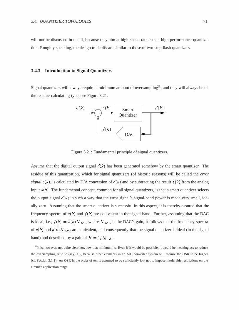
3.4. QUANTIZER TOPOLOGIES 71
will not be discussed in detail, because they aim at high-speed rather than high-performance quantiza-
tion. Roughly speaking, the design tradeoffs are similar to those of two-step-flash quantizers.
3.4.3 Introduction to Signal Quantizers
Signal quantizers will always require a minimum amount of oversampling29, and they will always be of
the residue-calculating type, see Figure 3.21.
QuantizerSmart d(k)e(k)g(k)
DACf(k)
Figure 3.21: Fundamental principle of signal quantizers.
Assume that the digital output signal d(k) has been generated somehow by the smart quantizer. The
residue of this quantization, which for signal quantizers (of historic reasons) will be called the error
signal e(k), is calculated by D/A conversion of d(k) and by subtracting the result f(k) from the analog
input g(k). The fundamental concept, common for all signal quantizers, is that a smart quantizer selects
the output signal d(k) in such a way that the error signal’s signal-band power is made very small, ide-
ally zero. Assuming that the smart quantizer is successful in this aspect, it is thereby assured that the
frequency spectra of g(k) and f(k) are equivalent in the signal band. Further, assuming that the DAC
is ideal, i.e., f(k) = d(k)KDAC where KDAC is the DAC’s gain, it follows that the frequency spectra
of g(k) and d(k)KDAC are equivalent, and consequently that the signal quantizer is ideal (in the signal
band) and described by a gain of K = 1=KDAC.
29It is, however, not quite clear how low that minimum is. Even if it would be possible, it would be meaningless to reduce
the oversampling ratio to (say) 1.5, because other elements in an A/D converter system will require the OSR to be higher
(cf. Section 3.1.1). An OSR in the order of ten is assumed to be sufficiently low not to impose intolerable restrictions on the
circuit’s application range.

72 CHAPTER 3. BASIC ASPECTS OF DATA CONVERSION
Nonideal DAC Effects Because all signal quantizers are of the residue-calculating type, they are sen-
sitive to DAC nonidealities. Figure 3.22 shows a model of the signal quantizer, where DAC nonidealities
are taken into account.
INLDAC[d(k)]
QuantizerSmarte(k)g(k)
f(k)
ODAC
DistortionOffset and
gdist(k)
DAC(ideal)KDAC
d(k)
Figure 3.22: Nonidealities caused by the feedback DAC.
As shown in Figure 3.22, the DAC’s offset and nonlinearity adds offset and distortion directly to the
input signal g(k). It is the sum gdist(k) which is quantized by the assumed ideal signal quantizer. In
other words, any signal quantizer will be as nonlinear as its internal DAC which is used to calculate
the residue of the quantization. This property is shared by all residue-calculating quantizers, including
residue-calculating data quantizers. A main advantage of signal quantizers is, however, that the error
signal e(k) does not have to be minimized in each sample because the smart quantizer can relocate
the corresponding error power to frequencies outside the signal band. In other words, d(k) can be a
low-resolution signal, and in particular, it can be a two-level signal.
The use of two-level output signals has for a long time been the preferred choice, because the DAC’s
INL error thereby will be zero30. In this way, DAC nonidealities will cause only gain and offset errors,
30For N = 2, the INL(n) consists of only those two points that define the DAC’s linear characteristic, i.e.,
INL(1) = INL(2) = 0. The same conclusion also follows from a simple manipulation of equations (3.28) and (3.31). Al-
though the DAC’s static performance will be perfectly linear, certain practical rules must be observed to obtain good dynamic
performance (of the one-bit DAC), which is a fundamental requirement in order to obtain good static and dynamic performance
of the quantizer (see [1]).

3.4. QUANTIZER TOPOLOGIES 73
whereby the implementation of inherently-linear quantizers is possible.
Nonideal Smart Quantizer Effects. While still allowing the smart quantizer to be somewhat unspec-
ified, the consequences of its potential nonidealities will be considered.
The main purpose of the smart quantizer is to minimize the signal-band power of the error signal e(k).
The success of this operation can be estimated from
Pinband[e(k)] = limN!1
�1
NTs
Z fb
�fb
jEobs(f)j2df�
(3.47)
where Eobs(f) is the Fourier spectrum of e(k) observed in a period of N samples, and where the signal
band is assumed to be the baseband jf j < fb.
Because signal quantizers need not have a good sample-to-sample equivalence between the analog input
g(k) and the digital output d(k), they are best evaluated using measures of their dynamic performance
(cf. Section 3.3). Thus, signal quantizers are typically described by their signal-to-error ratio (SER),
which can be estimated from
SER =Pinband[g(k)]
Pinband[e(k)]= lim
N!1
"R fb�fb
jGobs(f)j2dfR fb�fb
jEobs(f)j2df
#(3.48)
where g(k) and e(k) are observed in the same period of N samples.
For every 6 dB increase in the SER, the effective resolution of the signal quantizer is said to increase by
one bit. Proportionality can be assumed for high-resolution quantizers, i.e., a quantizer described by a
SER of 96 dB is said to have an effective resolution of 16 bits.
The SER measure is elsewhere called the quantizer’s signal-to-noise ratio (SNR). This practice has not
been adopted herein because it tends to lead to confusion. The source of e(k) is in general well known,
and its stochastic nature is, at best, only pseudo-random. Even when the smart quantizer is designed such
that e(k) does not include any detectable harmonics of g(k) (see [43]), the spectral composition of e(k)
is quite likely to be tonal. Furthermore, the time-domain equivalent of the signal-band part of e(k) can
have a peak-to-peak value which is significantly larger than 1 LSB, defined with respect to the quantizer’s

74 CHAPTER 3. BASIC ASPECTS OF DATA CONVERSION
effective resolution31 (see Chapter 3 in [1]). These problems are most serious when d(k) is a single-bit
signal, in which case the smart quantizer should be designed for a much better SER performance than
the SNR performance (limited by device noise). Although truly-stochastic noise cannot mask that the
error signal is tonal, this approach tends to make such quantizers more suitable for critical applications
(e.g. audio).
Design of Smart Quantizers. This section will discuss some of the properties that the smart quantizer
must possess, and how it can be implemented.
As discussed in Section 2.3, the accuracy with which a signal’s spectral composition can be estimated is
highly dependent on the duration of the observed signal. Thus, to effectively minimize the signal-band
power of e(k), the smart quantizer must choose each sample of d(k) on the basis of e(k) observed for
many (typically several thousand) samples. In other words, the smart quantizer must have memory.
In order to allow the error signal e(k) to be nonzero, the smart quantizer should minimize only the
signal-band spectral components of e(k), i.e. , it must allow e(k) to have substantial out-of-band power.
Equivalent to the band-pass-filter estimation method (see page 22), a filter H(f) is used to focus on the
spectral components of interest, i.e., the signal-band spectral components. The requirement of a long
observation time, combined with the preference for simple implementations, leads to the conclusion that
the filter should be of the infinite-impulse-response (IIR) type.
H(f)e(k) v(k) d(k)
Stage
Smart Quantizer
Smart
Figure 3.23: Fundamental elements in a smart quantizer.
Figure 3.23 shows the basic implementation of a smart quantizer, where the error signal e(k) is filtered
31In other words, the signal-band part of e(k) is often described by a large peak-to-rms ratio (it includes spikes), which
reflects that e(k) is not modeled well by a Gaussian stochastic process.
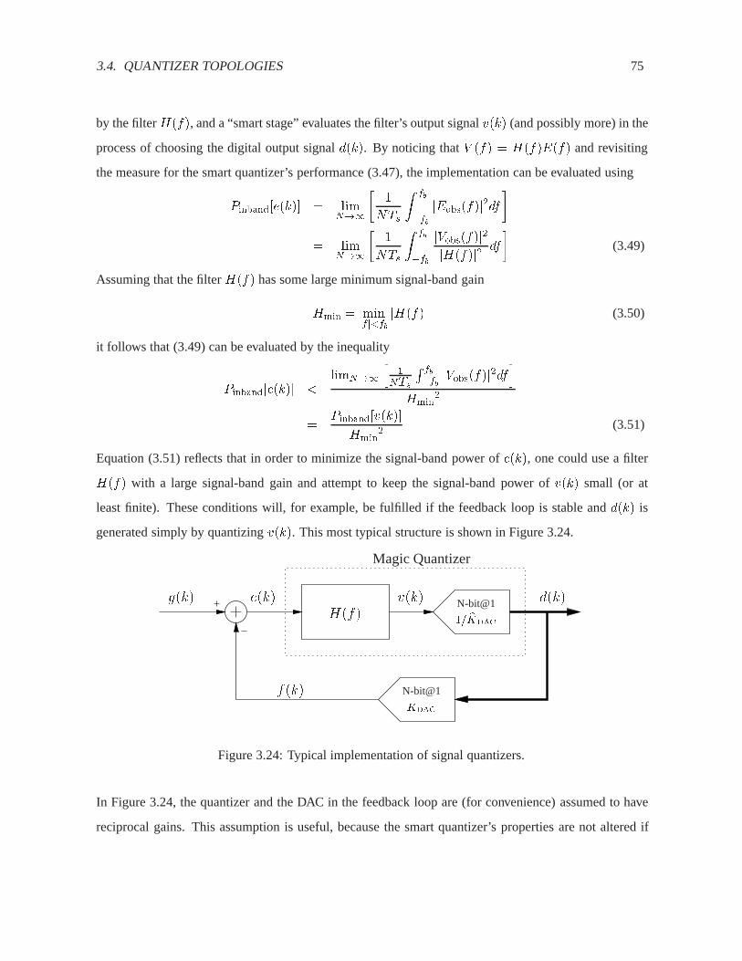
3.4. QUANTIZER TOPOLOGIES 75
by the filter H(f), and a “smart stage” evaluates the filter’s output signal v(k) (and possibly more) in the
process of choosing the digital output signal d(k). By noticing that V (f) = H(f)E(f) and revisiting
the measure for the smart quantizer’s performance (3.47), the implementation can be evaluated using
Pinband[e(k)] = limN!1
�1
NTs
Z fb
�fb
jEobs(f)j2df�
= limN!1
�1
NTs
Z fb
�fb
jVobs(f)j2jH(f)j2 df
�(3.49)
Assuming that the filter H(f) has some large minimum signal-band gain
Hmin = minjf j<fb
jH(f)j (3.50)
it follows that (3.49) can be evaluated by the inequality
Pinband[e(k)] <limN!1
h1
NTs
R fb�fb
jVobs(f)j2dfi
Hmin2
=Pinband[v(k)]
Hmin2 (3.51)
Equation (3.51) reflects that in order to minimize the signal-band power of e(k), one could use a filter
H(f) with a large signal-band gain and attempt to keep the signal-band power of v(k) small (or at
least finite). These conditions will, for example, be fulfilled if the feedback loop is stable and d(k) is
generated simply by quantizing v(k). This most typical structure is shown in Figure 3.24.
N-bit@1
KDAC
e(k)g(k)
f(k)
N-bit@1
1= bKDAC
Magic Quantizer
v(k) d(k)H(f)
Figure 3.24: Typical implementation of signal quantizers.
In Figure 3.24, the quantizer and the DAC in the feedback loop are (for convenience) assumed to have
reciprocal gains. This assumption is useful, because the smart quantizer’s properties are not altered if

76 CHAPTER 3. BASIC ASPECTS OF DATA CONVERSION
the filter and quantizer are scaled by reciprocal coefficients; also, the performance measures (Equations
(3.49) and (3.51)) are not affected by this assumption. Thus, assuming that the resolving range of
the internal quantizer is sufficiently wide, the system’s stability can be evaluated using any traditional
stability criteria, e.g. Nyquist’s Stability Criterion. The traditional design approach is, however, to
design
NTF(f) =1=KDAC
1 +H(f)(3.52)
as a high-pass filter32 with some pre-calculated characteristic, for example a Chebychev Type-II high-
pass-filter response. NTF(f) is called the signal quantizer’s noise transfer function, because it deter-
mines the output-referred linear signal processing of the internal quantizer’s truncation error33.
Although Figure 3.24 shows the most common implementation for signal quantizers, it is not the op-
timal way to implement the smart quantizer. Obviously, it is not an optimal design34 when g(k) must
be included in e(k) and filtered before it can appear in the output d(k). An improvement can be ob-
tained simply by directly informing the smart quantizer about g(k), so that it can be taken into account
immediately. Figure 3.25 shows a simple signal quantizer implemented according to this principle.
N-bit@1
KDAC
N-bit@1
1= bKDAC
e(k)
f(k)
v(k)H(f)
g(k) d(k)
Smart Quantizer
Figure 3.25: Improved implementation of signal quantizers.
Figure 3.26 shows the same signal quantizer as shown in Figure 3.25 redrawn. It is included to shed
32More generally, as a filter that suppresses the signal-band.33Which too often is modeled as noise (cf. the discussion on page 38).34Because the object is to minimize e(k).

3.4. QUANTIZER TOPOLOGIES 77
some light on the fundamental operation; compare Figures 3.17, 3.25, and 3.26.
H(f)
g(k)
Offset
e(k)
d(k)
f(k)
Figure 3.26: Model of the signal quantizer shown in Figure 3.25.
It is worthwhile to notice that the topology shown in Figure 3.25 also assures that the signal transfer
function becomes independent of the filter H(f)
STF(f) =Ffd(k)gFfg(k)g =
1= bKDAC[1 +H(f)]
1 + [KDAC= bKDAC]H(f)' 1
KDAC(3.53)
The advantage of designing the signal quantizer as shown in Figure 3.25, rather than using the traditional
topology shown in Figure 3.24, is only significant if g(k) has substantial sample-to-sample variation.
That is, however, always the case when the oversampling ratio is low, which is the general assumption
in this work.
This concludes the introduction to signal quantizers. They will be discussed in greater detail in Chapter 4.

78 CHAPTER 3. BASIC ASPECTS OF DATA CONVERSION

Chapter 4
State-of-the-Art Signal Quantizers
This chapter will provide an overview of state-of-the-art techniques used for the implementation of
signal quantizers. The advantages and shortcomings of the techniques will be discussed and serve as
background for the discussion in the subsequent chapters. The reader is assumed to be familiar with
Chapters 2 and 3, especially the introduction to signal quantizers provided in Section 3.4.3.
First, it will be explained why single-bit signal quantizers are not suitable for high-resolution wide-
bandwidth quantization. Aspects, such as stability and technology constraints, will be considered to
reach this conclusion.
Second, signal quantizers implemented in the so-called MASH topology will be discussed. In princi-
ple, this technique can improve the performance to an almost unlimited extent, but in reality, circuit
imperfections will significantly limit the achievable improvement.
Third, it will be argued that mismatch-shaping DACs facilitate the implementation of linear multi-bit
signal quantizers. In this way, the desired high-resolution wide-bandwidth signal quantizers can be
implemented. The basic techniques will be described, and some shortcomings will be identified.
79

80 CHAPTER 4. STATE-OF-THE-ART SIGNAL QUANTIZERS
Terminology. The remaining part of this work will discuss several topologies for the implementation
of data converters1 that attempt to minimize the signal-band power of nonlinear errors. Figures 3.24
and 3.25 illustrate only the most basic principle for such signal quantizers, and to distinguish these
topologies easily from the new topologies to be discussed, it is convenient to have a separate name for
these two structures.
For historic reasons, signal quantizers of the type shown in Figures 3.24 and 3.25 will be called delta-
sigma (��) quantizers2. If the digital output signal d(k) has a resolution of N bits, the structures
are said to be N -bit delta-sigma quantizers. Notice that N refers to the actual resolution, i.e., not the
effective resolution, which typically is much higher (cf. page 73).
4.1 Single-Bit Delta-Sigma Quantizers
A single-bit DAC can provide only two output levels. Assuming that these two levels are time-invariant
and that dynamic errors are avoided3, such DACs are inherently linear. This is because any static char-
acteristic S(n) consisting of only two elements will define a straight line (the linear characteristic) with
respect to which the DAC has an ideal static performance. As with any other DAC, single-bit DACs are
subject to linear errors (offset and gain errors), but such errors are generally tolerable.
General Structure of a Delta-Sigma A/D Converter System. Figure 4.1 illustrates the implementa-
tion of a typical delta-sigma A/D converter system. The �� quantizer employs a single-bit DAC in the
feedback path, which ensures that the quantizer is not subject to nonlinear DAC errors (cf. page 72).
In brief, the operation can be described as follows. The analog front end filters and samples the input
signal a(t) and provides the discrete-time analog signal g(k). The single-bit �� quantizer converts g(k)
1In principle, such data converters should be called signal converters, but this name has not been widely adopted.2Digital circuits implemented in the same topology are called delta-sigma modulators. Digital delta-sigma modulators are
used to reduce the resolution of a signal while preserving its signal-band spectral composition.3This is feasible for switched-capacitor implementations, for which good circuit techniques have been developed. Similar
techniques for current-mode DACs are under development.

4.1. SINGLE-BIT DELTA-SIGMA QUANTIZERS 81
Filter
Multi-Rate
KDAC
1-Bit@1
fs = OSR � 2fN
Anti-Aliasing
Sampler H(f)
f(k)
a(t) e(k) d(k) u(k)v(k)
“1=KDAC”
1-Bit@1
fs = 2fN
g(k)
Figure 4.1: A/D converter system based on a single-bit �� quantizer.
into d(k) in such a way that the signal-band spectral composition of the two signals are linearly related.
Outside the signal band, the spectral compositions will differ substantially. A digital filter will reject
the out-of-band spectral components of d(k), thereby generating a highly oversampled signal, which is
decimated to a signal-band-equivalent signal u(k) sampled at a much lower sampling frequency.
Evaluation of the Topology. The main advantages of the approach shown in Figure 4.1 are that the
analog front end is simple to implement, and that the quantization process is inherently linear despite
possible analog circuit imperfections. The analog portion of the system is highly oversampled; hence
the anti-aliasing filter can be implemented as a simple filter of low order (cf. Equation (3.5)). The ��
quantizer is a simple circuit, the performance of which depends mainly on the linearity of the input-stage
integrator used for the implementation of the loop filter H(f) (see [43]).
The need for the somewhat complex digital multi-rate filter is a disadvantage, but as the layout density
has increased and the power consumption of digital circuits has been reduced over time, this tradeoff
for avoiding complex analog circuitry has become quite acceptable. Hence, single-bit �� ADCs are
suitable for the implementation of many high-resolution applications in modern technologies, which
typically are optimized for the design of digital circuits.
4.1.1 Obtaining and Preserving Stability
Useful stability criterions for the closed-loop operation of single-bit �� quantizers are very hard to
derive. This problem is caused by the single-bit loop quantizer (the internal single-bit data quantizer),

82 CHAPTER 4. STATE-OF-THE-ART SIGNAL QUANTIZERS
which is so nonlinear that its linear characteristic is not even defined (cf. Section 3.1.4).
A single-bit data quantizer is just a polarity detector that assigns one of two integers to d(k). Hence, if
the input signal v(k) has a small standard deviation4 (relative to the difference of the two levels provided
by the DAC), the quantizer is, in a sense, described by a large gain (relative to 1=KDAC); whereas
if the standard deviation of v(k) is large, the quantizer’s “gain” is low. Despite this highly nonlinear
property of single-bit data quantizers, many attempts to analyze single-bit �� quantizers’ stability have
been based on the model shown in Figure 4.2, where it is assumed that q(k) is an externally-applied
uniformly-distributed white-noise signal, and where the single-bit loop quantizer’s gain is assumed to be
1=KDAC, i.e., independent of v(k).
H(f)
f(k)
g(k) e(k) d(k)v(k)
q(k)
1KDAC
KDAC
Figure 4.2: Linear model, which often has been used to model single-bit �� quantizers.
Not surprisingly, the linear model has proven to be so oversimplified that in many situations it is almost
useless. An example in which the model leads to the incorrect conclusion is the closed-loop system’s
stability evaluated using Nyquist’s Stability Criterion.
Figure 4.3 shows a correct nonlinear model of the closed-loop system, where q(k) is modeled as a
deterministic function T1 of v(k). Without going into detail, notice that stability should be construed
as v(k) having the property of being bounded in magnitude. The stability properties are often ana-
lyzed/evaluated by considering a pseudo-probability-density-function (PPDF) description of v(k), i.e.,
a histogram of v(k) obtained from a finite-duration simulation. “Stability” is indicated if most (say
99.9%) of the PPDF[v(k)] is well within the single-bit loop quantizer’s resolving range (cf. Figure 4.3),
but it is not an accurate measure that will guarantee stability. The problem is, in part, complicated by
4The use of this measure should not be construed to be that v(k) is a stochastic signal; it is not.
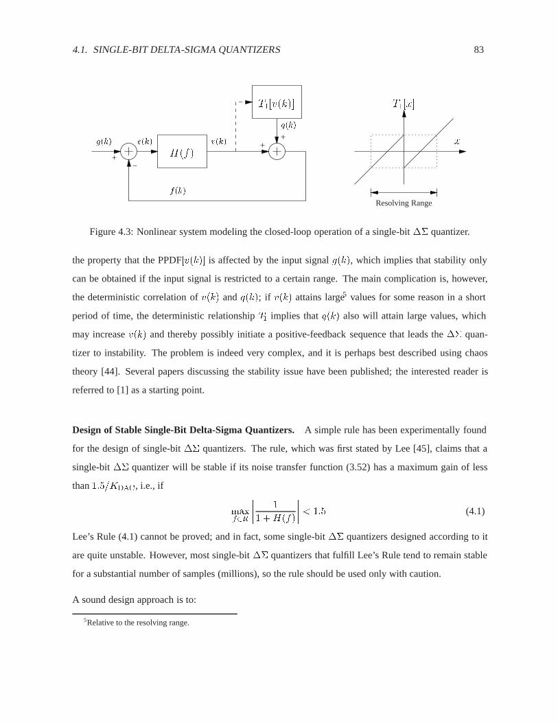
4.1. SINGLE-BIT DELTA-SIGMA QUANTIZERS 83
Resolving Range
H(f)
f(k)
g(k) e(k) v(k)
T1[v(k)] T1[x]
x
q(k)
Figure 4.3: Nonlinear system modeling the closed-loop operation of a single-bit �� quantizer.
the property that the PPDF[v(k)] is affected by the input signal g(k), which implies that stability only
can be obtained if the input signal is restricted to a certain range. The main complication is, however,
the deterministic correlation of v(k) and q(k); if v(k) attains large5 values for some reason in a short
period of time, the deterministic relationship T1 implies that q(k) also will attain large values, which
may increase v(k) and thereby possibly initiate a positive-feedback sequence that leads the �� quan-
tizer to instability. The problem is indeed very complex, and it is perhaps best described using chaos
theory [44]. Several papers discussing the stability issue have been published; the interested reader is
referred to [1] as a starting point.
Design of Stable Single-Bit Delta-Sigma Quantizers. A simple rule has been experimentally found
for the design of single-bit �� quantizers. The rule, which was first stated by Lee [45], claims that a
single-bit �� quantizer will be stable if its noise transfer function (3.52) has a maximum gain of less
than 1:5=KDAC, i.e., if
maxf2R
���� 1
1 +H(f)
���� < 1:5 (4.1)
Lee’s Rule (4.1) cannot be proved; and in fact, some single-bit �� quantizers designed according to it
are quite unstable. However, most single-bit �� quantizers that fulfill Lee’s Rule tend to remain stable
for a substantial number of samples (millions), so the rule should be used only with caution.
A sound design approach is to:
5Relative to the resolving range.

84 CHAPTER 4. STATE-OF-THE-ART SIGNAL QUANTIZERS
� design a �� quantizer according to (4.1),
� simulate the �� quantizer extensively and re-design it if necessary, and
� assure the stability by making the loop filter nonlinear, for example as described below.
A Toolbox [46] can be used to simplify the first two steps of this design procedure.
Nonlinear Loop Filters. The stability of a single-bit �� quantizer can be assured by incorporating
simple nonlinearities in an otherwise linear loop filter H(f). Linear loop filters can be implemented
in several ways, but the following discussion will consider only the fourth-order structure shown in
Figure 4.4. This type of loop filter is a good choice for analog �� quantizers [43], and the reader should
find no difficulty in generalizing the discussion to other filter orders or structures.
v(k)
�1 �2 �3 �4
e(k)
� 1 � 2
z�1
1�z�11
1�z�1z�1
1�z�11
1�z�1
Integrator–4Integrator–3Integrator–1 Integrator–2
Figure 4.4: Example of a loop-filter structure.
The loop filter’s poles, which will become the noise transfer function’s (3.52) zeroes, will be located on
the z-plane unit circle6 at angles (frequencies) determined by the coefficients i that are used to tune the
two resonators. The feed-forward coefficients �i are used to control the noise transfer function’s poles.
A �� quantizer, which is based on this loop filter, will be stable only if the output of all integrators
remain bounded. By simple inspection of the loop filter’s topology, it should be observed that the output
of each integrator is a function of e(k) only.
6The z-plane refers to the z-transform, i.e., the Fourier transform, for which the variable substitution z = ej2�fTs is used.

4.1. SINGLE-BIT DELTA-SIGMA QUANTIZERS 85
Preserving stability is somewhat comparable to backing a truck with as many trailers as the number of
integrators less one, where the output of each integrator is modeled as the orientation of each trailer.
Obviously, backing the trailer train is a difficult task; hence instability is quite likely to occur. The
visualization corresponding to Lee’s Rule is that the trailers’ lengths must be an increasing function of
their distance from the driver. Although this model is somewhat inconsistent mathematically, it may aid
the understanding of how and why the following very efficient stabilization technique works.
The stabilization technique is quite simple. If and when instability occurs, i.e., if v(k) becomes a se-
quence of large values, the last-stage (the fourth) integrator is reset. If this action does not restore
stability, then the two last integrators are reset shortly afterwards. This process is continued (more and
more integrators are reset) until stability is restored. In practice, it will never be necessary to reset the
two first integrators, and the effective noise shaping will always be of at least second order7.
Achievable Performance. The implication of Lee’s Rule may not be obvious, but a study will show
that the OSR that is required to obtain a signal-band Signal-to-quantization-Error-Ratio (SER) of (say)
100 dB is only a slowly-decreasing function of the loop filter’s order. This is illustrated in Figure 4.14
in [1], where the derivation also can be found. Table 4.1 summarizes the result expressed as the OSR
required to obtain 100 dB SER. Clearly, 10 times oversampling is not enough to achieve this level of
effective resolution when using a single-bit �� quantizer with a loop filter of any reasonable order.
In fact, at 10 times oversampling, the SER will be around 40 dB for all well-designed single-bit ��
quantizers of high order.
Filter Order 1 2 3 4 5 6 7 8
OSR >1000 220 90 56 45 36 32 30
Table 4.1: OSR required to obtain 100 dB SER for single-bit �� quantizers.
7The term “noise shaping” refers to the filtering performed on q(k) in the linear model, Figure 4.2. The effective order of
noise shaping is (in this thesis) defined as the maximum number of signal-band unit-circle poles the linear filter can have while
obtaining a bounded output.
86 CHAPTER 4. STATE-OF-THE-ART SIGNAL QUANTIZERS
4.1.2 Bandwidth Limitation
The signal bandwidth equals the sampling frequency divided by twice the OSR (3.3); for this reason
wide-bandwidth �� quantization requires either a high sampling frequency or a low OSR.
As discussed above, the stability properties of single-bit �� quantizers restricts the choice of the loop
filter such that high-resolution �� quantization cannot be obtained using these quantizers at less than
approximately 30 times oversampling. Furthermore, for high-order �� quantizers, the digital multi-rate
filter must have a narrow transition band, which drastically complicates its implementation. At high
speed, the power consumption of the digital circuitry becomes more of an issue, so medium-order ��
quantizers operating at an OSR of about 50 will typically be preferred.
Increasing the sampling frequency implies an increase in the power consumption of both the analog and
digital circuitry. Assuming that the �� quantizer is implemented as a switched-capacitor circuit in a
modern technology8, the sampling frequency is hard to increase beyond 20–50 MHz, even if the power
consumption is allowed to be as large as 100–500 mW. The speed/power tradeoff is of course dependent
on the technology of choice, but improvements from this source do not seem to keep pace with market
requirements. It is unlikely that high-performance switched-capacitor circuits that are implemented in
standard technologies will be clocked much faster than (say) 100 MHz in the coming few years.
By combining the estimates made above, it follows that the bandwidth of a high-resolution single-bit ��
ADC is unlikely to exceed 1 MHz within a reasonable time frame. Furthermore, to obtain a competitive
advantage, bandwidth improvements should be obtained either by lowering the OSR or by increasing
the sampling frequency without increasing the power consumption or the production cost.
Continuous-Time Loop Filter. An interesting approach, which can be used to increase the sampling-
frequency/power-consumption ratio in almost any technology, is to implement the �� quantizers with
continuous-time loop filters. These so-called continuous-time (CT) �� quantizers have several ad-
vantages (noise, power, and bandwidth), but also substantial drawbacks; they are very sensitive to the
8As of 1998.
4.2. MASH TOPOLOGY 87
dynamic errors of the DAC in the feedback path, and particularly they are very sensitive to clock-jitter-
induced errors (cf. page 52). Hence the resolution reported thus far has been quite modest. Some exotic
continuous-time �� quantizers have been implemented in highly specialized technologies and operated
at sampling frequencies in the GHz range [47]. Such high-speed �� quantizers will obviously require
the use of extremely fast and power-consuming digital circuits. The SNR performance reported was
approximately 30 dB less than the theoretical SER, which indicates that clock-jitter and other dynamic
errors were the limiting factors.
4.2 MASH Topology
The limiting factor of single-bit �� quantizers operating at low oversampling ratios is that the loop
filter’s H(f)minimum signal-band gain cannot be increased beyond a certain level without encountering
stability problems; consequently, the error signal’s e(k) inband spectral power density cannot be lowered
to less than a certain minimum. Now referring to the nonlinear model shown in Figure 4.3, it can easily
be shown that d(k) = f(k)=KDAC can be calculated from
D(f) = G(f)1
KDAC� H(f)
1 +H(f)+Q(f)
1
KDAC� 1
1 +H(f)
= G(f)STF(f) +Q(f)NTF(f) (4.2)
where the two terms represent the signal and the error spectra, respectively. Although Q(f) often has
an approximately uniform spectral power density in the entire frequency spectrum (which is why it is
often modeled as white noise) it should be understood that it is not noise, but merely the single-bit loop
quantizer’s truncation error. Because q(k) is not noise, it can be estimated, A/D converted, filtered by a
digital filter that imitates NTF(f), and the result subtracted from d(k) to compensate for the error term
Q(f)NTF(f) in (4.2). This so-called MASH9 quantizer is shown in Figure 4.5.
9The name MASH is claimed to be an abbreviation for Multi-Stage Noise Shaping, but it is also claimed that the name was
chosen from a popular TV show (for whatever reasons).

88 CHAPTER 4. STATE-OF-THE-ART SIGNAL QUANTIZERS
H(f)
f(k)
g(k) 1-Bit@2N
d(k)
1=KDAC�2
KDAC�2
1-Bit@2N
KDAC
1-Bit@2N
1= bKDAC�2
N-Bit@1�q(k)
dMASH(k)
dNTF(f)
v(k)e(k)
dq(k)
dcomp(k)
Figure 4.5: MASH-topology signal quantizer.
4.2.1 Analysis of the MASH Topology
The MASH topology includes a traditional residue stage (cf. Figure 3.17) for the calculation of the
residue of the single-bit quantization of v(k). As discussed in Section 3.4.2, the gain of a residue stage’s
quantizer is determined uniquely by the gain KDAC�2 of the residue stage’s DAC; consequently, the
single-bit loop quantizer will – by definition – have a gain of 1=KDAC�2. This definition does not alter
the single-bit �� quantizer’s stability properties, but it uniquely determines the noise transfer function
NTF(f), by which q(k) is filtered in its appearance in d(k). The noise transfer function is calculated
from
NTF(f) =1=KDAC�2
1 +H(f) KDACKDAC�2
(4.3)
Estimation of the Residue. Because d(k) is a single-bit signal, the residue, �q(k), of the single-bit
quantization of v(k) can be calculated with very good accuracy (except for an unimportant offset). A
multi-bit quantizer10 A/D converts �q(k), and the result dq(k) is filtered by a digital filter dNTF(f) and
10Originally, this quantizer was a single-bit �� quantizer, but the generalization to include data quantizers is trivial, and a
high-resolution, say pipeline, quantizer is typically a better choice [48].

4.2. MASH TOPOLOGY 89
then added to the single-bit output d(k).
Nonlinearity of the Multi-Bit Quantizer. Nonlinearity of the multi-bit quantizer is only a minor issue.
Nonlinearity will cause an error in dq(k), which contains harmonic distortion of q(k). For this purpose,
q(k) can be modeled very well as a white-noise signal, and hence dq(k) will include a white-noise error
with a total power determined by the linearity of the quantizer, i.e., typically 40–60 dB less than the
power of q(k). Considering that dNTF(f) will efficiently suppress this error in the signal band, it will be
understood that the quantizer’s nonlinearity will not be the limiting factor unless more than 40–60 dB
improvement (relative to Equation (4.2)) needs to be obtained.
Gain Error of the Multi-Bit Quantizer. Using the same kind of argument as above, it can be under-
stood that a slight inaccuracy of the multi-bit quantizer’s gain is acceptable. Assuming that bKDAC�2
matches KDAC�2 with (say) �40 dB relative accuracy, it follows that the error term Q(f)NTF(f) in
(4.2) is suppressed by 40 dB, which would be a significant improvement relative to the performance
when dcomp(k) = 0.
Mismatch of Transfer Functions. Mismatch of the single-bit �� quantizer’s noise transfer function
(4.3) and the digital filter dNTF(f) meant to implement it11 is the only (but highly) critical factor in the
MASH topology.
The error term in the digital output dMASH(k) can be described as
Derror(f) = Q(f)
"1=KDAC�2
1 + KDACKDAC�2
H(f)� 1bKDAC�2
dNTF(f)
#(4.4)
Assuming (for the reasons discussed above) that KDAC�2 and bKDAC�2 match, the error term can be
simplified to
Derror(f) ' Q(f)bKDAC�2
"1
1 + KDACKDAC�2
H(f)� dNTF(f)
#(4.5)
11Except for the gain factor 1=KDAC�2, which is implemented by the multi-bit quantizer

90 CHAPTER 4. STATE-OF-THE-ART SIGNAL QUANTIZERS
In general, KDAC and KDAC�2 will have the same nominal value, therefore the digital filter dNTF(f)
will be designed to have the same transfer function as the nominal value of 1=(1 +H(f)).
Ideally, the difference in Equation (4.5) will be zero. The success of the MASH topology is in general
evaluated as the resulting improvement of the SER, which can be estimated asR fb�fb
jdNTF(f)j2dfR fb�fb
����� 1
1+KDAC
KDAC�2H(f)
� dNTF(f)
�����2
df
(4.6)
Considering that the numerator in (4.6) is a very small number, it follows that the difference in (4.5)
must be very small to obtain a significant improvement.
Minimization of the denominator of (4.6) is, in theory, a matter of matching two rational functions, one
having slightly inaccurate coefficients due to the imperfections of the analog circuitry. The imperfections
will manifest themselves as a dislocation of the noise transfer function’s poles and zeroes, where each
dislocation will result in a nonzero term in the denominator of (4.6). Without going into great detail, the
generally accepted12 conclusion is that the achievable improvement becomes less and less as the order of
the loop filter is increased; hence the MASH topology is mainly of interest for low-order �� quantizers.
Stability concerns are actually another reason why the MASH topology is useful for low-order ��
quantizers only. High-order �� quantizers will generally require that nonlinearities be incorporated in
the loop filter (cf. page 84), and it will be very complicated to incorporate the “inverse” nonlinearities indNTF(f) to cancel the difference in (4.5).
Typical Design Approach. For the reasons discussed above, MASH quantizers are almost always
based on a second-order first-stage �� quantizer. The classical design technique is to choose the nomi-
nal value of H(f) as
H(f) =z�1(2� z�1)
(1� z�1)2; z = ej2�fTs (4.7)
12According to the author’s own survey, this is the general understanding of most experts. Because a much more robust
technique has been developed (which is discussed in the third part of this thesis), the author has not directly attempted to
optimize the design of MASH quantizers.
4.2. MASH TOPOLOGY 91
in which case the digital compensation filter is a simple second-order FIR filter:
dNTF(f) = (1� z�1)2; z = ej2�fTs (4.8)
This design, however, does not fulfill Lee’s Rule (4.1), and hence the single-bit loop quantizer’s input
signal v(k) will significantly exceed the quantizer’s resolving range. Although the �� quantizer will
remain stable13, this overload operation implies that the multi-bit quantizer must have a resolving range
that is significantly (15-20 dB) larger than what normally would be expected. The corresponding draw-
back is that the system becomes the same 15-20 dB more sensitive to errors caused by nonlinearity of
the multi-bit quantizer, which therefore must be designed to have a quite high performance. If the OSR
is low, say 10, the digital compensation filter (4.8) will only suppress signal-band white-noise errors by
about 40 dB, which (because the single-bit loop quantizer is overloaded) implies that the multi-bit quan-
tizer must have the same linearity and resolution as the overall system less 3-4 bits. A main advantage
is, however, that the multi-bit quantizer’s nonlinearity will not cause harmonic distortion of the input
signal, but instead, a colored pseudo-noise error.
Improved Second-Order MASH Quantizer? Although it has not yet been attempted14, it seems that
a substantial advantage can be obtained simply by scaling H(f) with a factor (say 0.25) or change it
otherwise to conform with Lee’s Rule, in which case the multi-bit quantizer can be designed to have a
smaller resolving range. Because another much improved topology has been discovered (presented in
the third part of this thesis), this approach has not been analyzed thoroughly.
Conclusion. MASH quantizers are, in principle, wonderful signal quantizers; but in reality, they suffer
greatly from imperfections of the analog circuitry.
Dislocation of the noise transfer function’s poles and zeroes require the quantizer to be of low order. If
the oversampling ratio is fairly high, a better performance can generally be obtained using a simpler-to-
implement higher-order single-bit �� quantizer. If the oversampling ratio is low, the MASH quantizer
13Second-order quantizers will always be stable, but they are not necessarily well-behaved, i.e., although v(k) will be
bounded, it can attain large values.14As far as the author is aware.

92 CHAPTER 4. STATE-OF-THE-ART SIGNAL QUANTIZERS
will become somewhat sensitive to nonlinearity of the multi-bit quantizer, which possibly can be avoided
by scaling the loop filter properly.
Some successful implementations of wide-bandwidth MASH quantizers have been reported [48,49], but
the effective resolution is barely 15-16 bits. This resolution is probably close to the limit of what can
be obtained, because these quantizers were designed with great care by highly-qualified designers, who
employed many circuit tricks to make the analog circuitry behave as ideally as possible.
In an attempt to improve the cancellation of the truncation error, a technique to adaptively adjust the
digital compensation filter has been developed [50]. However, the effective resolution obtained thus far
does not exceed 12-13 bits at 8 times oversampling.
4.3 Multi-Bit Delta-Sigma Quantizers
To obtain inherent linearity, �� quantizers have traditionally been restricted to have a single-bit output
signal. The low resolution is, however, associated with numerous disadvantages, among which are
the quantizer’s poor stability and the large magnitude of q(k). Section 4.4 will discuss the so-called
mismatch-shaping D/A converters, which can provide an inherently-linear multi-bit D/A conversion
with a very good signal-band performance. Mismatch-shaping D/A converters should be considered as a
major breakthrough, because they facilitate the use of multi-bit �� quantizers, which (in the absence of
DAC errors) can be designed to have a much better performance than their single-bit counterparts. The
following discussion of multi-bit �� quantizers refers to Figure 3.25.
Brute-Force Improvement. Because the magnitude of the multi-bit loop quantizer’s truncation error
is inversely proportional to the resolution of d(k), every doubling of the resolution will result in 6 dB
improvement of the SER. Hence, assuming that the loop filter is designed in the same way as for a
single-bit �� quantizer (cf. page 83), d(k) will need to be of 10-bit resolution to obtain 100 dB SER
at 10 times oversampling15. Fortunately, significantly better results can be obtained if the loop filter is
re-designed.
15As discussed in Section 4.1, single-bit �� quantizers of any high order will provide a SER of only about 40 dB.

4.3. MULTI-BIT DELTA-SIGMA QUANTIZERS 93
4.3.1 Stability Properties
A main advantage of multi-bit �� quantizers is that their stability properties are much better than for
their single-bit counterparts, and hence their design need not be restricted as much as proposed by Lee’s
Rule (4.1).
In essence, NTFmax = maxf j1=(1+H(f))j is the main factor that controls the rms value16 of v(k), and
Lee’s Rule is merely an empirical estimate of when v(k) is expected to be small enough not to overload
a single-bit data quantizer. However, for a multi-bit �� quantizer, where it will be assumed that the
input signal g(k) is somewhat smaller (say by �5 LSB) than the loop quantizer’s resolving range, v(k)
may have significant fluctuation (�5 LSB) without causing overload of the loop quantizer, and hence
the loop filter can be designed to have a larger NTFmax than imposed by Lee’s Rule.
An Example. Figure 4.6 shows the sinusoid input signal g(k) and the staircase output signal d(k) for
two quite different designs of a 6th-order 17-level �� quantizer operating at eight times oversampling17.
The upper plot corresponds to an aggressively-designed quantizer, for which NTFmax = 8, whereas the
lower plot corresponds to a more conservatively-designed quantizer, for which NTFmax = 2.
Clearly, d(k) is more “busy” for the aggressive design than it is for the conservative design. This property
is in good agreement with the prediction made above. Although the total power of the error signal e(k)
is larger for the aggressive �� quantizer, it is actually 41 dB less is the signal band (assuming eight
times oversampling) than for the conservative �� quantizer. However, Figure 4.6 indicates that the
aggressive �� quantizer’s input signal should be considered to be full-scale, whereas the conservative
�� quantizer supposedly will remain stable for inputs that are as much as 5 dB larger18. Hence, “only”
36 dB improvement is obtained by using the aggressive loop filter.
16More precisely, the standard deviation of the PPDF[v(k)] (cf. Section 4.1.1).17OSR = 8 is used because the Figures are based on simulations that constitute a partial reproduction of work performed by
Richard Schreier [2].18The quantizer becomes unstable when the loop quantizer’s resolving range (�8:5 LSB) is exceeded.
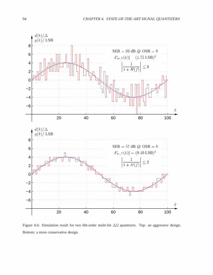
94 CHAPTER 4. STATE-OF-THE-ART SIGNAL QUANTIZERS
20 40 60 80 100
−6
−4
−2
0
2
4
6
8
20 40 60 80 100
−6
−4
−2
0
2
4
6
8
SER = 98 dB @ OSR = 8
SER = 57 dB @ OSR = 8
Pav[v(k)] = (1:75 LSB)2���� 1
1 +H(f)
���� � 8
Pav[v(k)] = (0:40 LSB)2���� 1
1 +H(f)
���� � 2
k
k
d(k)=�g(k)= LSB
d(k)=�g(k)= LSB
Figure 4.6: Simulation result for two 6th-order multi-bit �� quantizers. Top: an aggressive design.
Bottom: a more conservative design.

4.3. MULTI-BIT DELTA-SIGMA QUANTIZERS 95
Achievable Performance. The advantages that can be obtained by increasing the value of NTFmax are
discussed in [2], in which Figure 5 illustrates the SER performance that can be obtained at eight times
oversampling using quantizers of various orders and for various values of NTFmax.
The result is summarized here in Table 4.2. SER1LSB is the SER obtained when the input is a sinusoid
with a peak-to-peak magnitude of 1 LSB. The minimum resolution of d(k) must be approximately
6pPav[v(k)]= LSB to assure stability. In this limit, the considered 1- LSB input signal g(k) is full-
scale, and the loop quantizer’s resolving range is used mainly for fluctuations in v(k). If d(k) is of
higher resolution, the wider resolving range can be utilized to increase the input signal’s magnitude,
which will result in a 6 dB improvement for every factor of two increase in the magnitude of g(k) (cf.
Equation (4.9)).
Quantizer Order (OSR = 8) 2 3 4 5 6 7 8
SER1LSB/dB forpPav[v(k)] < 1 LSB 38 49 56 62 65 68 70
SER1LSB/dB forpPav[v(k)] < 1:5 LSB 38 52 62 70 76 81 85
SER1LSB/dB forpPav[v(k)] < 2 LSB 38 52 65 74 82 88 94
SER1LSB/dB forpPav[v(k)] < 3 LSB 38 52 65 78 87 95 101
SER1LSB/dB forpPav[v(k)] < 5 LSB 38 52 65 78 91 100 108
SER ' SER1LSB + 6 dB log2
"N �
6pPav[v(k)]
LSB
!#(4.9)
Table 4.2: The SER performance that can be obtained from a N -level �� quantizer operating at eight-
times oversampling.
As will be discussed in the Section 4.4, mismatch-shaping D/A converters will typically be of fairly low
resolution, say 4 to 5 bits or even less.
Consider a design where the resolution of d(k) is 5 bits and the loop filter is designed such thatpPav[v(k)] = 5 LSB
Although the �� quantizer’s resolving range is quite small (a few LSBs), the maximum SER can still
be made as high as 108–120 dB (using a high-order loop filter). However, a characteristic of this design

96 CHAPTER 4. STATE-OF-THE-ART SIGNAL QUANTIZERS
is that the �� quantizer’s feedback signal f(k) is many times larger than the input signal g(k), therefore,
the system’s performance is very sensitive to the feedback DAC’s nonlinearity and noise performance.
In general, this should not be considered a good design; usually it is preferable to have a (relatively)
larger resolving range for g(k), even if a lower SER is an unavoidable tradeoff.
Conclusion. A fluctuation in v(k) of about �3pPav[v(k)] is expected, and the loop quantizer’s re-
solving range must be at least this wide to preserve stability. An increment in the resolution of d(k)
beyond this minimum will affect (improve) only the �� quantizer’s resolving range19, and (as for any
other quantizer) the maximum SER will improve 6 dB for every doubling of the system’s resolving
range.
The SER is not the only design aspect that needs to be considered, and the circuit designer should, in
general, choose an entry in Table 4.2, for which the feedback DAC’s resolution N is at least twice as
large as 6pPav[v(k)]. For example, if the feedback DAC’s resolution is (say) N = 16, then the loop
filter should be designed according to the second entry row in Table 4.2. The �� quantizer’s resolving
range will be approximately (16� 9) LSBs = 7 LSBs, therefore, the second term in Equation (4.9) will
be approximately 17 dB. Accordingly, to obtain a 100 dB SER, the loop filter must be of at least the 8th
order.
Because the resolution N in general will be low, the second factor in Equation (4.9) will be less than 30
dB, and hence higher-order20 loop filters will be required to obtain 100 dB SER performance.
For continuous-time implementations, the feedback DAC is usually a current-mode DAC, and clock
jitter is another (important) reason not to use a loop filter for which 6pPav[v(k)]= LSB is too close to
N (cf. Section 3.2.3).
19The �� quantizer’s resolving range can be estimated as N � LSB� 6pPav[v(k)] (cf. Equation (4.9)).
20Fifth order will be the minimum, and 6th- and 7th-order loop filters will be typical.

4.4. MISMATCH-SHAPING DACS 97
4.4 Mismatch-Shaping DACs
As described in the previous section, many advantages can be obtained if an inherently-linear more-than-
two-level DAC is available. Considering that the multi-bit DAC will be used as the feedback element in a
multi-bit �� quantizer, it should be understood that it need not be ideal in the entire frequency spectrum;
the �� quantizer’s performance is fairly insensitive to errors outside the signal band, and hence (errors
cannot generally be avoided) the DAC should preferably optimize only the signal-band performance.
DACs that have this characteristic will in the following be referred to as mismatch-shaping DACs.
Mismatch-shaping DACs assume that their output will be evaluated as a signal21, and they attempt to
keep the signal-band part of the generated signal free of errors by allowing mismatch-induced errors to
occur at other frequencies. Accordingly, mismatch-shaping DACs and signal quantizers alike are based
on the same fundamental philosophy, namely, that the error signal is applied to a filter that has high
gain in the signal band, and that the system is controlled such that the filter’s output remains bounded in
magnitude.
A main difference between signal quantizers and mismatch-shaping DACs is in the way they calculate
the error signal. Signal quantizers make use of a supposedly-ideal22 DAC to calculate the error signal
(cf. Figure 3.21). Mismatch-shaping DACs, on the other hand, cannot use the same technique because
that will require the existence of an ideal reference DAC, as shown in Figure 4.7. In the absence of
an ideal reference DAC, it will be impossible to calculate and filter the mismatch-shaping DAC’s error
signal m(k) in the analog domain, but nevertheless (as it will be explained in the following) it is actually
possible to use digital techniques to control certain properties of the error signal m(k).
21Meaning that the output is evaluated by its spectral composition, and not sample by sample.22The performance is evaluated with respect to the signal band only.

98 CHAPTER 4. STATE-OF-THE-ART SIGNAL QUANTIZERS
H(f)
d(k) f(k)DrivingDAC
DACReference
m(k)n(k)
Figure 4.7: Conceptual mismatch-shaping DAC.
4.4.1 Estimation of the Error Signal
In the following, it will be assumed that the DAC is implemented in the topology shown in Figure 4.8,
where a digital front end separates d(k) into a set of signals bi(k) such that
d(k) =
P�1Xi=0
bi(k) (4.10)
The composite DAC’s linear-characteristic gain Kd and offset fo�set are defined as shown in Figure 3.15.
When calculated with respect to this linear characteristic, the DAC’s nonlinearity m(k) = INLd[d(k)]
can be expressed with respect to the characteristics of the individual DACs as follows:

4.4. MISMATCH-SHAPING DACS 99
c0(k)
c1(k)
c2(k)
c3(k)
cP�1(k)KP�1
d(k)
b0(k)
b1(k)
b2(k)
b3(k)
bP�1(k)
f(k)
Digital
Front-End
(Separator)
K0
K1
K2
K3
Figure 4.8: Fundamental topology of a typical mismatch-shaping DAC.
m(k) = f(k)� [Kdd(k) + fo�set]
=
P�1Xi=0
[Kibi(k) + ci;o�set + INLi[bi(k)]] � [Kdd(k) + fo�set]
=P�1Xi=0
[Kdbi(k) + [Ki �Kd]bi(k) + ci;o�set + INLi[bi(k)]]� [Kdd(k) + fo�set]
=
"P�1Xi=0
[Kdbi(k)]�Kdd(k)
#These terms cancel (= 0)
+
"P�1Xi=0
[ci;o�set]� fo�set
#These terms cancel (= 0)
+
P�1Xi=0
[[Ki �Kd]bi(k) + INLi[bi(k)]]
=P�1Xi=0
[bi(k)[Ki �Kd]] +P�1Xi=0
INLi[bi(k)] (4.11)
Accordingly, the DAC’s nonlinearity INLd[d(k)] can be considered to consist of two terms:
� the error termPP�1
i=0 [bi(k) [Ki �Kd]] will be called the gain mismatch errors, because each term
in the sum reflects an error that is caused by mismatch of the respective DAC’s gain relative to the
composite DAC’s gain.

100 CHAPTER 4. STATE-OF-THE-ART SIGNAL QUANTIZERS
� the error termPP�1
i=0 INLi[bi(k)] will be called the local nonlinearity errors, because each term
in the sum reflects an error caused by the respective DAC’s nonlinearity with respect to its own
(local) linear characteristic.
Notice that if the individual DACs consist of only one element, the local nonlinearity errors become zero,
and the composite DAC’s nonlinearity INLd[d(k)] will consist of the gain mismatch errors only. Hence,
Equation (4.11) agrees with the previously derived expressions (3.37) and (3.40) for the nonlinearity
INLd[d(k)] of binary-weighted DACs and unit-element DACs, respectively.
Unknown Parameters. Equation (4.11) is in reality not an estimation of the error signal m(k), but
merely a description based on several unknown parameters and functions:
K0;K1; : : : ;KP�1 and INL0; INL1; : : : ; INLP�1 (4.12)
Obviously, one could attempt to measure these parameters as accurately as possible, and then estimate
m(k) on the basis of (4.11). That would, however, be a very tedious approach. It would also be a
somewhat silly approach, because one could instead employ digital correction [1] [3] [4], which would
be much simpler to implement and also provide better results.
Mismatch-shaping DACs avoid the complexity of estimating analog parameters using digital techniques
(that are not based on knowledge of the parameter’s (4.12) value) for the minimization23 of the signal-
band power of m(k). Hence, mismatch-shaping DACs have an advantage in that they are very robust
with respect to low-frequency variations24 of the parameters (4.12).
4.4.2 First-Order Unit-Element Mismatch-Shaping DACs
The so-called unit-element mismatch-shaping (UE-MS) DACs [2, 5–18] are based on an array of nomi-
nally-identical analog sources, which are controlled by each one of the single-bit signals bi(k) (for
simplicity, the following will assume that the signals bi(k) attain only the two values 0 and 1).
23The use of this term should not be construed to be that the mismatch-shaping DAC actually finds a minimum, but merely
that it tries to reduce the signal-band power of m(k).24For example, caused by aging of the circuit or by changes in the ambient temperature, humidity, etc..

4.4. MISMATCH-SHAPING DACS 101
The linear-characteristic gain Kd was calculated in Equation (3.39), and according to (4.11), the nonlin-
earity m(k) = INLd[d(k)] can be described as
m(k) =
P�1Xi=0
[bi(k)(Ki �Kd)] +
P�1Xi=0
INLi[bi(k)]
=P�1Xi=0
[bi(k)(Ki �Kd)] (4.13)
The main characteristic of all first-order-shaping systems – whether it is a �� quantizer/modulator or a
mismatch-shaping DAC – is that the integral (sum) of the error signal remains bounded in magnitude.
To evaluate this property for unit-element DACs, the integrated error signal n(k) can be calculated as
n(k) =
kXj=0
m(j)
=kX
j=0
"P�1Xi=0
[bi(j)(Ki �Kd)]
#
=
P�1Xi=0
24 kXj=0
[bi(j)(Ki �Kd)]
35=
P�1Xi=0
24(Ki �Kd)kX
j=0
[bi(j)]
35 (4.14)
Because the composite DAC’s gain Kd is the average value of the individual DACs’ gains’ Ki (cf.
Equation (3.39)), it follows that
P�1Xi=0
(Ki �Kd) = 0 (4.15)
This fundamental property (4.15), which is valid for all unit-element DACs, can be used to bring Equa-
tion (4.14) to the form
n(k) =P�1Xi=0
24(Ki �Kd)
24 kXj=0
[bi(j)] � q
3535 for all real q (4.16)
By defining the set U = f0; 1; 2; : : : ; (P � 1)g and applying Schwartz’s inequality to (4.16), it follows

102 CHAPTER 4. STATE-OF-THE-ART SIGNAL QUANTIZERS
that
jn(k)j �P�1Xi=0
24jKi �Kdj������kX
j=0
[bi(j)] � q
������35
� maxi2U
fjKi �KdjgP�1Xi=0
������kX
j=0
[bi(j)] � q
������� max
i2UfjKi �Kdjg � P �max
i2U
8<:������kX
j=0
[bi(j)] � q
������9=; for all real q (4.17)
The term P �maxi2U fjKi �Kdjg is a constant for each implementation25, therefore, the unit-element
DAC will perform first-order mismatch-shaping, i.e., jn(k)j will be bounded in magnitude, if s(k) is
bounded
s(k) = minq2R
8<:maxi2U
8<:������kX
j=0
[bi(j)] � q
������9=;9=; (4.18)
Considering thatPk
j=0 [bi(j)] represents the number of times that the i’th DAC has been used to convert
bi = 1, it follows that s(k) simply represents the difference in usage
s(k) =maxi2U
nPkj=0 [bi(j)]
o�mini2U
nPkj=0 [bi(j)]
o2
(4.19)
Hence, the simple condition required for baseband first-order mismatch shaping is that all of the unit-
element DACs must be employed equally often (on average).
Simple Explanations of How and Why First-Order Mismatch-Shaping Works. The basic concept
on which all baseband first-order mismatch-shaping DACs are based, can be expressed as follows:
Baseband mismatch-shaping DAC’s will emphasize the performance at low frequencies (in
particular the average value of the output). When all elements are used the same number
of times, their corresponding errors will have canceled, and hence the average value will be
correct.
25More precisely, it is a stochastic variable, which will attain a constant value for each independent implementation.

4.4. MISMATCH-SHAPING DACS 103
Alternatively, the operation can be expressed as:
Let a unit-element DAC consist of the set A of unit elements. When a sample is D/A
converted using the set B0 � A of unit elements, an error Æ will occur. To assure a good
low-frequency performance, this error must be corrected as soon as possible by an error
�Æ. The error Æ is unknown, but (as expressed by Equation (4.15)) the error �Æ can be
committed by using the set B0 = A n B0 of unit elements. Hence, the set B0 of unused
elements should be used before any of the already-used elements B0 are used again; when
all elements A are used, the next (of the remaining part of a) sample can be D/A converted
using any new set B1 � A of unit elements, and the procedure is repeated.
Element-Rotation Scheme. The element-rotation scheme (ERS) is possibly the simplest algorithm
for the implementation of baseband first-order UE-MS mismatch-shaping DACs.
As illustrated in Figure 4.9, the unit elements are arranged in a fixed order and used sequentially. For
example:
If the first sample is of value 4, then the first four unit elements b0 � b3 are turned on. If the
next sample is of value 3, then the next three elements b4 � b6 are turned on. This procedure
continues until all the elements are used once, at which time the pointer “wraps around” as
shown in Figure 4.9, where the third sample, of value 5, causes b7 � b8 and b0 � b2 to be
turned on.
Figure 4.10 shows the implementation of a digital front end that provides the ERS switching function
illustrated in Figure 4.9. The digital input d(k) is assumed to be binary coded and attain only integer
values in the range from 0 to 8. A rotation pointer (cf. Figure 4.9) is generated by accumulating d(k)
modulo 8. The input d(k) is binary-to-thermometer encoded (cf. Equation (3.41)), and the thermometer-
coded representation of d(k) is rotated stepwise (in steps of 4,2,1) according to the rotation pointer,
which will always attain an integer value in the range from 0 to 7.

104 CHAPTER 4. STATE-OF-THE-ART SIGNAL QUANTIZERS
������
Rotation Pointer
b0 b1 b2 b3 b4 b5 b6 b7 b8
d(0) = 4
d(1) = 3
d(2) = 5
d(3) = 5
d(4) = 7
Figure 4.9: The element-rotation scheme, which is used for the implementation of baseband first-order
unit-element mismatch-shaping DACs.
����������
A
B
A+
B
Binary-to-
Therm
ometer
Encoder
D-L
atch
b0(k)b1(k)b2(k)b3(k)b4(k)b5(k)b6(k)b7(k)
Rotate by 0/4 Rotate by 0/2 Rotate by 0/1
d(k) )Rotation Pointer
msb
lsb
0/1
0/2
0/4
0/8
0/1
0/1
0/1
0/1
0/1
0/1
0/1
0/1
0/4
0/2
0/1
Figure 4.10: An implementation of the ERS algorithm.
4.4. MISMATCH-SHAPING DACS 105
Other Implementations. The term Data-Weighted-Averaging (DWA) DACs will refer to all baseband
first-order mismatch-shaping D/A converters, which can be implemented in infinite variations. The
differences lie typically in the complexity of the digital front end, in how small they manage to keep
s(k) in (4.19), and in the spectral composition of n(k). Descriptions of several implementations can be
found in [2, 5–18].
The ERS algorithm was discussed in this context because it was the first known implementation [5], and
because it is fairly simple to implement.
4.4.3 Performance of First-Order Mismatch-Shaping DACs
The term baseband first-order mismatch-shaping comes from the property that n(k) =Pk
j=0m(j) will
be of finite power, and hence that the spectral properties of the error signal m(k) can be calculated from
M(f) = N(f) � (1� z�1); where z = e2�fTs (4.20)
Equation (4.20) implies that M(0) = 0, but otherwise it is not straightforward to estimate M(f) accu-
rately. Often N(f) is assumed to be white noise, and although simulations provide some justification
for this assumption, it should be understood that this model is typically oversimplified and that it may
lead to very inaccurate estimates of the system’s performance.
Idle Tones. Idle tones are often encountered in single-bit �� quantizers when the truncation error q(k)
(cf. Figure 4.2) attains pseudo-periodic patterns, in which case q(k) is poorly modeled as white noise.
The consequence is that the �� quantizer’s actual SER may be significantly less than the SER predicted
on the basis of the white-noise assumption for q(k). Even worse, idle tones may imply that a ��
quantizer is less suitable for critical applications such as audio (cf. page 74). The idle-tone problem is
known to be quite troublesome for low-order �� quantizers, and in particular for first-order quantizers.
Dither, a noise signal that is deliberately added to v(k) (cf. Figure 4.2), is known to be an efficient means
to prevent26 idle tones (cf. Chapter 3 in [1]).
26Unfortunately, the dither signal must be so large that it tends to cause instability in single-bit �� quantizers, so (in reality)
it is very hard to efficiently avoid idle tones in single-bit �� quantizers.

106 CHAPTER 4. STATE-OF-THE-ART SIGNAL QUANTIZERS
Idle tones are also a serious problem in many DWA DACs [51]. Consider for example, the ERS DWA
DAC illustrated in Figure 4.9. If the input is constant (say d(k) = 3), the output will be generated by the
periodic use of three groups of three unit elements each, and the error signal m(k) will be of the form
m(k) = : : : ; Æ1; Æ2; Æ3; Æ1; Æ2; Æ3; Æ1; Æ2; Æ3; : : : (4.21)
where Æ1+ Æ2+ Æ3 = 0. Hence, the error signal m(k) will be a tone at the frequency fs=3. If the tone is
not located in the signal-band, then the behavior may be acceptable; but if a tone is in the signal-band,
the behavior is highly unacceptable because the DAC functions partly as an in-band oscillator.
For idle tones to become a problem for baseband DACs, the pseudo-periodic patterns in m(k) must have
period(s) which are at least 2 � OSR long, and that is actually quite likely to occur [51].
A DWA DAC’s digital front end can be designed (more or less successfully) to avoid idle tones. The
so-called butterfly scrambler [9] is, for example, claimed to be less tonal than the simpler ERS front
ends, partly because it uses more combinations to generate each nominal value. The general idea is
to assure that the signals bi(k) are “complicated” functions of the input signal d(k). An example of
how to implement “intentional complexity” was presented by Williams [39], who designed a DWA
front end comprising three ERS encoders for the control of the same array of 9 unit elements. For
each input sample, only one of the three ERS encoders is activated, i.e., clocked and used to control
the unit elements, depending on which of the three controlling sets B0 = f0; 3; 6g, B1 = f1; 4; 7g,
B2 = f2; 5; 8g the input sample d(k) is a member of. Williams claims that this technique efficiently
prevents idle tones, but this author claims that some tones are still likely27 to occur.
Some improved techniques to avoid idle tones are described in the second part of this thesis.
Estimation of the Error Signal’s Signal-Band Power. Assuming that the digital front end efficiently
avoids idle tones, i.e., that it is reasonable to model N(f) in (4.20) as white noise, it is fairly simple to
estimate the signal-band performance of DWA DACs.
27The previous example, where d(k) = 3 will result in the same performance; signals where d(k) (for example) has the
period f1; 4; 7; 7; 4; 1g will generate tones at fs=6; etc.

4.4. MISMATCH-SHAPING DACS 107
Assume that the ERS algorithm28 is used for a DWA DAC with P unit elements, and that the the rotation
pointer is equally likely to attain any of the P values: f0; 1; 2; : : : ; (P � 1)g. Assume further that each
of the unit elements Xi; i 2 f1; 2; : : : ; Pg represents a stochastic event of the same (Gaussian) N (1; �2)
process (normalized with respect to 1 LSB).
When the rotation pointer attains the value q, the standard deviation �n(q) of n(k) =Pk
j=0m(k) =Pqi=1[Xi]� q
P
PPi=1[Xi] can be calculated from
�n(q) = � LSB
rq(P � q)
P(4.22)
implying that the average power of n(k) can be estimated roughly (for large P ) as29
Pav[n(k)] =�2 LSB2
P
P�1Xq=0
q(P � q)
P' P�2 LSB2
6(4.23)
Because m(k) is the first-order difference of n(k), the signal-band power of m(k) can be estimated as
Pav;inband[m(k)] =P�2
6
"1
�
Z �=OSR
0(1� e�j!)2d!
#
=P�2 LSB2
6Sh(OSR; 1) (4.24)
where Sh(OSR; 1) is the first-order-shaping signal-band gain factor, which is shown graphically in Fig-
ure 4.11.
Estimating the Signal-Band Signal. To evaluate the DWA DAC’s performance, the error signal’s
signal-band power should be related to a full-scale signal. Assuming that the DWA DAC is used as the
feedback element in a multi-bit �� quantizer, it makes the most sense to relate the error signal to a
full-scale input signal g(k).
Recall from Section 4.3.1 that to obtain a high SER from a multi-bit �� quantizer with a low-resolution
feedback DAC, the loop filter H(f) must be designed with a fairly high NTFmax value, in which case
28This assumption is justifiable. Idle-tone-free ERS front ends will be discussed in the second part of this thesis.29This is the average value for multiple implementations of the same circuit. The reader is referred to [52] for an analysis of
the yield aspect.
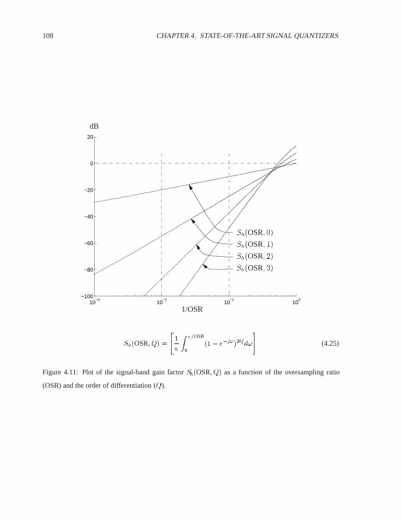
108 CHAPTER 4. STATE-OF-THE-ART SIGNAL QUANTIZERS
10−3
10−2
10−1
100
−100
−80
−60
−40
−20
0
20
Sh(OSR; 1)
Sh(OSR; 2)
Sh(OSR; 3)
Sh(OSR; 0)
1/OSR
dB
Sh(OSR; Q) =
"1
�
Z �=OSR
0(1� e�j!)2Qd!
#(4.25)
Figure 4.11: Plot of the signal-band gain factor Sh(OSR; Q) as a function of the oversampling ratio
(OSR) and the order of differentiation (Q).
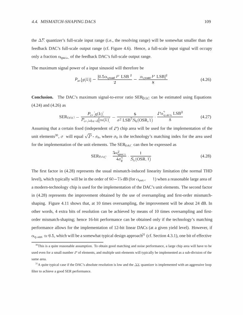
4.4. MISMATCH-SHAPING DACS 109
the �� quantizer’s full-scale input range (i.e., the resolving range) will be somewhat smaller than the
feedback DAC’s full-scale output range (cf. Figure 4.6). Hence, a full-scale input signal will occupy
only a fraction �quant of the feedback DAC’s full-scale output range.
The maximum signal power of a input sinusoid will therefore be
Pav[g(k)] =[0:5�quantP LSB]2
2=
[�quantP LSB]2
8(4.26)
Conclusion. The DAC’s maximum signal-to-error ratio SERDAC can be estimated using Equations
(4.24) and (4.26) as
SERDAC =Pav[g(k)]
Pav;inband[m(k)]=
6
�2 LSB2Sh(OSR; 1)� P�
2quant LSB2
8(4.27)
Assuming that a certain fixed (independent of P ) chip area will be used for the implementation of the
unit elements30, � will equalpP � �0, where �0 is the technology’s matching index for the area used
for the implementation of the unit elements. The SERDAC can then be expressed as
SERDAC =3�2quant4�20
� 1
Sh(OSR; 1)(4.28)
The first factor in (4.28) represents the usual mismatch-induced linearity limitation (the normal THD
level), which typically will be in the order of 60�75 dB (for �quant = 1) when a reasonable large area of
a modern-technology chip is used for the implementation of the DAC’s unit elements. The second factor
in (4.28) represents the improvement obtained by the use of oversampling and first-order mismatch-
shaping. Figure 4.11 shows that, at 10 times oversampling, the improvement will be about 24 dB. In
other words, 4 extra bits of resolution can be achieved by means of 10 times oversampling and first-
order mismatch-shaping; hence 16-bit performance can be obtained only if the technology’s matching
performance allows for the implementation of 12-bit linear DACs (at a given yield level). However, if
�quant ' 0:5, which will be a somewhat typical design approach31 (cf. Section 4.3.1), one bit of effective
30This is a quite reasonable assumption. To obtain good matching and noise performance, a large chip area will have to be
used even for a small number P of elements, and multiple unit elements will typically be implemented as a sub-division of the
same area.31A quite typical case if the DAC’s absolute resolution is low and the �� quantizer is implemented with an aggressive loop
filter to achieve a good SER performance.
110 CHAPTER 4. STATE-OF-THE-ART SIGNAL QUANTIZERS
resolution will be lost, and it can only be re-gained by using a slightly higher oversampling ratio or by
providing better matching of the unit elements.
Several options are available to avoid the requirement for an intolerably low relative matching index
�0. First of all, the quantizer can (and often should) be designed such that �quant is fairly close to one,
which (however) may require the DAC to be of fairly high resolution. Generally, at most 6-bit resolution
will be of interest for UE-MS DACs employed in �� quantizers, because a flash quantizer of the same
resolution is required for the implementation of the loop quantizer, and because the complexity of the
digital DWA front end and of the routing to the unit elements increases with the resolution. If even
higher resolution is needed, the use of a higher oversampling ratio may be an option (provides 9 dB
improvement for each doubling of the OSR), but this should be used only as a last resort. A simple
post-processing or power-up calibration may be an alternative worth considering because the required
degree of matching (say �0 � 10�4) usually can withstand aging of the circuit and/or changes in the
ambient temperature, etc.. Also, a change of the topology may be a feasible option. Considering that
the �� quantizer’s signal-band performance has been successfully improved by increasing the order
of the loop filter, it seems plausible that higher-order mismatch-shaping techniques may yield an even
better signal-band suppression of the mismatch errors. Sh(OSR; 2) in Figure 4.11 shows that, if m(k)
can be made the second-order difference of a white-noise signal n2(k) with the same power as n(k),
approximately 6 bits (as opposed to just 4 bits) extra performance relative to the normal THD level can
be obtained at OSR=10. The next section will investigate the possibility and evaluate the performance.
4.4.4 Second-Order Mismatch-Shaping DACs
The object of this section is to analyze digital front ends (encoders), which can provide second-order
mismatch shaping of an array of unit elements. Such an encoder was first published by Yasuda [53] and
other techniques have been published by Schreier [12] and Galton [14]. The following discussion will
focus on the tree-structure encoder proposed by Galton, because it is the simplest known implementation
(complexity is a drawback for these encoders).

4.4. MISMATCH-SHAPING DACS 111
Definitions. The following discussion will assume that the mismatch-shaping encoder controls an ar-
ray of 2N unit elements Xi; i 2 f1; 2; 3; : : : ; 2Ng, where N is an integer. LetA0 denote the set of these
unit elements
A0 = fX1; X2; : : : ;X2N g (4.29)
and let Ki denote the gain of the single-bit DAC implemented by the unit element Xi.
The object of the following is to use the set A0 of unit elements to D/A convert the digital signal d(k)
in such a way that the D/A conversion’s error signal m(k) can be considered to be generated by filtering
a finite-power signal n(k) with an appropriate filter 1=H(f). More particularly, the desired mismatch-
shaping operation is defined by the relations
f(k) = Dfd(k);A0;H(f)g= K[A0]d(k) +m(k)
= K[A0]d(k) + n(k) � h�1(k) (4.30)
where K[A0] denotes the average value (i.e. the linear-characteristic gain) of the elements inA0; n(k)�h�1(k) denotes the convolution of n(k) and h�1(k); n(k) is required to be bounded in magnitude; and
h�1(k) is the impulse response of 1=H(f).
Figure 4.12 shows the symbol that will be used to represent a mismatch-shaping DAC based on the set
A0 of unit-elements. The number of oriented arcs encircling A0 represents the order of the mismatch-
shaping encoder (second-order mismatch shaping is indicated).
A0
d(k) f(k) = K[A0]d(k) + n(k) � h�1(k)
Figure 4.12: Symbol representing a second-order unit-element mismatch-shaping DAC, based on the set
A0 of unit elements.
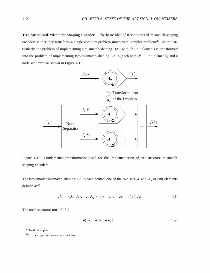
112 CHAPTER 4. STATE-OF-THE-ART SIGNAL QUANTIZERS
Tree-Structured Mismatch-Shaping Encoder. The basic idea of tree-structured mismatch-shaping
encoders is that they transform a single complex problem into several simpler problems32. More par-
ticularly, the problem of implementing a mismatch-shaping DAC with 2N unit elements is transformed
into the problem of implementing two mismatch-shaping DACs (each with 2N�1 unit elements) and a
node separator as shown in Figure 4.13.
A1
d1(k)
A2
d2(k)
d(k) f(k)
SeparatorNode
A0
d(k) f(k)
Transformation
of the Problem
Figure 4.13: Fundamental transformation used for the implementation of tree-structure mismatch-
shaping encoders.
The two smaller mismatch-shaping DACs each control one of the two sets A1 and A2 of unit elements
defined as33
A1 = fX1;X2; : : : ;X2(N�1)g and A2 = A0 n A1 (4.31)
The node separator must fulfill
d(k) = d1(k) + d2(k) (4.32)
32Divide et impera!33I.e. , A is split in two sets of equal size.
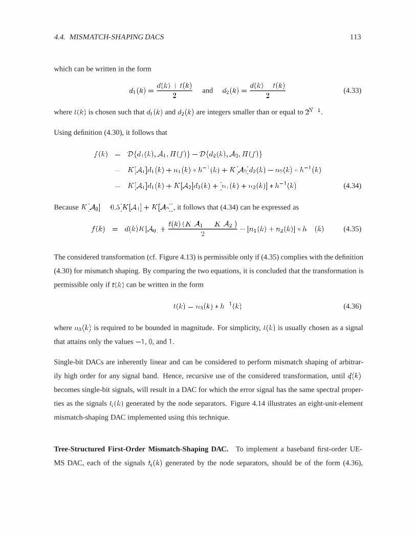
4.4. MISMATCH-SHAPING DACS 113
which can be written in the form
d1(k) =d(k) + t(k)
2and d2(k) =
d(k)� t(k)
2(4.33)
where t(k) is chosen such that d1(k) and d2(k) are integers smaller than or equal to 2N�1.
Using definition (4.30), it follows that
f(k) = Dfd1(k);A1;H(f)g+Dfd2(k);A2;H(f)g= K[A1]d1(k) + n1(k) � h�1(k) +K[A2]d2(k) + n2(k) � h�1(k)= K[A1]d1(k) +K[A2]d2(k) + [n1(k) + n2(k)] � h�1(k) (4.34)
Because K[A0] = 0:5[K[A1] +K[A2]], it follows that (4.34) can be expressed as
f(k) = d(k)K[A0] +t(k) (K[A1]�K[A2])
2+ [n1(k) + n2(k)] � h�1(k) (4.35)
The considered transformation (cf. Figure 4.13) is permissible only if (4.35) complies with the definition
(4.30) for mismatch shaping. By comparing the two equations, it is concluded that the transformation is
permissible only if t(k) can be written in the form
t(k) = n3(k) � h�1(k) (4.36)
where n3(k) is required to be bounded in magnitude. For simplicity, t(k) is usually chosen as a signal
that attains only the values �1, 0, and 1.
Single-bit DACs are inherently linear and can be considered to perform mismatch shaping of arbitrar-
ily high order for any signal band. Hence, recursive use of the considered transformation, until di(k)
becomes single-bit signals, will result in a DAC for which the error signal has the same spectral proper-
ties as the signals ti(k) generated by the node separators. Figure 4.14 illustrates an eight-unit-element
mismatch-shaping DAC implemented using this technique.
Tree-Structured First-Order Mismatch-Shaping DAC. To implement a baseband first-order UE-
MS DAC, each of the signals ti(k) generated by the node separators, should be of the form (4.36),
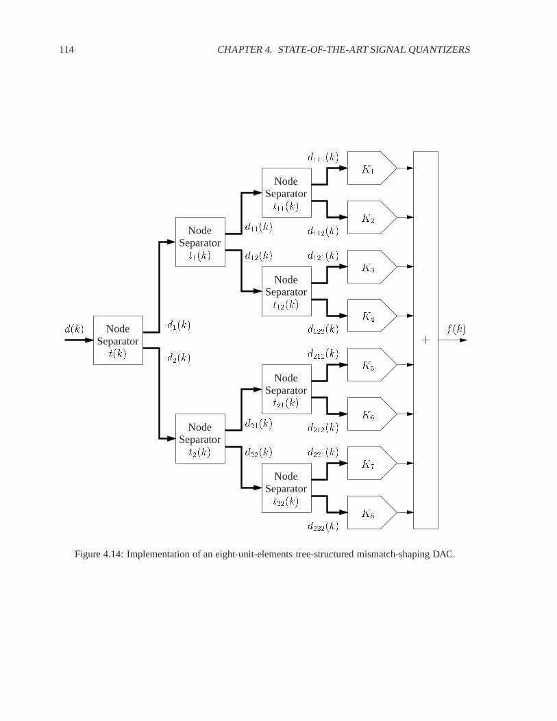
114 CHAPTER 4. STATE-OF-THE-ART SIGNAL QUANTIZERS
f(k)d1(k)
d2(k)
d111(k)
d121(k)
d122(k)
d221(k)
d222(k)
d212(k)
d112(k)
K1
K2
K3
K4
K6
K7
K8
K5
d211(k)
Node
NodeSeparator
NodeSeparator
NodeSeparator
NodeSeparator
NodeSeparator
NodeSeparator
t(k)
t11(k)
t12(k)
t21(k)
t22(k)
t2(k)
t1(k)
Separatord(k)
d22(k)
d12(k)
d11(k)
d21(k)
Figure 4.14: Implementation of an eight-unit-elements tree-structured mismatch-shaping DAC.

4.4. MISMATCH-SHAPING DACS 115
where h�1(k) = f1;�1; 0; 0; 0; : : : g. In other words, the signals ti(k) must each fulfill
9W for which
������kX
j=0
ti(j)
������ < W for all k (4.37)
Equation (4.37) can be fulfilled for W = 1. Consider, for example, the first node separator. When
d(k) is an even number, then t(k) is chosen as 0 because d(k) can be split evenly into d1(k) and d2(k).
However, when d(k) is odd, either d1(k) or d2(k) must be one larger than the other, i.e., jt(k)j = 1.
By choosing t(k) of the opposite polarity to that ofPk�1
j=0 t(j), it follows that (4.37) will be fulfilled
for W = 1; consequently first-order mismatch-shaping is obtained. This operation can be implemented
using only a few logic gates and a toggle flip-flop for each node separator.
Tree-Structured Band-Pass Mismatch-Shaping DAC. Assume that the signal band is a small fre-
quency range centered around fs=4. With respect to this signal band, a first-order UE-MS DAC can be
implemented as described above, except that now h�1(k) = f1; 0; 1; 0; 0; 0; : : : g.
Tree-Structured Second-Order Mismatch-Shaping DAC. The implementation of a second-order
mismatch-shaping tree-structured DAC is, in principle, the same as that of the first-order one described
above. The only difference is in the generation of the signals ti(k). For a baseband DAC, the object is to
assure that the second-order sum of t(k) remains bounded, a task which can be implemented by means
of a �� quantizer (shown in Figure 4.15).
�
�1
LSB of d(k)
0=1t(k)1
1� z�1�z�1
1� z�1n(k)
Figure 4.15: Node separator for use in a tree-structured second-order mismatch-shaping DAC.
116 CHAPTER 4. STATE-OF-THE-ART SIGNAL QUANTIZERS
The output of the single-bit truncation element decides the polarity of the next nonzero t(k) value. The
multiplier at the truncator’s output assures that t(k) will be nonzero only when d(k) is odd.
The multiplier is, in reality, the main problem for UE-MS encoders of orders higher than 1 because long
sequences of even numbers will deactivate the quantizer’s feedback and possibly thereby cause large
values of n(k). Consider, for example, a situation where the outputs of both integrators equal 1 and the
following 10 values of d(k) are even. During this period of even values, the output of the first integrator
will remain constant 1, whereas the second integrator’s output will increase to 11. Only then, when d(k)
finally attains an odd value, can the quantizer attempt to control the state variables.
A second-order node separator is in principle unstable34, but usually d(k) will attain odd values once
in a while, in which case stability can be preserved35. In a best-case scenario, d(k) will be odd/even
according to a stochastic process for which both outcomes are equally likely to occur, and in which there
is no sample-to-sample correlation.
4.4.5 Performance of Second-Order Mismatch-Shaping DACs
The following will estimate the performance of first-order and second-order tree-structured UE-MS
DACs on the basis of simulations. The simulations will be based on the assumption that for each sample
and for each node separator, it is entirely random whether jti(k)j is one or zero. This assumption favors
the second-order mismatch-shaping DACs, but even then, the conclusion turns out to be in favor of
first-order systems; hence the assumption is acceptable for this purpose.
Estimating the Error Signal. The performance is determined by the spectral properties of the DACs’
error signal, which can be expressed as (cf. Equation (4.35))
m(k) = t(k)Æ + [n1(k) + n2(k)] � h�1(k) where Æ =(K[A1]�K[A2])
2(4.38)
34In the strict sense.35Reset operations will most likely be necessary on certain occasions.

4.4. MISMATCH-SHAPING DACS 117
Considering that n1(k) � h�1(k) and n2(k) � h�1(k) are the error signals from the two D/A conver-
sions Dfd1(k);A1;H(f)g and Dfd2(k);A2;H(f)g, which are implemented by completing the tree
(cf. Figures 4.13 and 4.14), it follows that
m(k) = t(k)Æ
+[t1(k)Æ1 + t2(k)Æ2]
+[t11(k)Æ11 + t12(k)Æ12 + t21(k)Æ21 + t22(k)Æ22]
+ : : :
=Xi
ti(k)Æi (4.39)
Provided the above assumption, each of the signals ti(k) will have the same spectral power density,
hence the performance can be simulated and evaluated on the basis of the spectral properties of only a
single t(k) signal.
Simulation Results. A node separator was simulated for H(f) = 11�z�1 (first order) and for H(f) =
5�3z�1
(1�z�1)2(second-order36). The estimated spectral power densities of the two t(k) signals obtained are
shown in Figure 4.16. The DFTs are based on each 16384 samples; and for clarity, they have been
smoothed with a 10-tap moving-average filter.
For the first-order mismatch-shaping encoder, the spectral power density of t(k) is approximately pro-
portional to the frequency, which is the expected performance (cf. Equation (4.20)). Ideally, the spectral
power density of the t(k) signal generated by the second-order encoder should be proportional to the
second power of the frequency, which can actually be observed at low frequencies. However, at higher
frequencies (f > fs=10), the spectral power density is fairly constant. Hence, the OSR must be high to
take advantage of the more efficient suppression of low-frequency errors.
The different behavior of first- and second-order encoders can be explained as follows. A first-order
encoder is in “standby” mode when t(k) = 0, and it will make use of the first available chance (i.e., as
soon as jt(k)j = 1) to correct the accumulated error. A second-order encoder, on the other hand, is not in
36This seems to be a good design, compared to simulation results obtained for other � values (cf. Figure 4.15).

118 CHAPTER 4. STATE-OF-THE-ART SIGNAL QUANTIZERS
10−2
10−1
100
0
−40
−80
First-Order
Second-Order
2f=fs
dB DFT[t(k)]
Figure 4.16: Spectral composition of the control signal t(k) when d(k) is equally likely to be odd/even
and when there is no sample-to-sample correlation.
10−2
10−1
100
0
−40
−80
Second-Order
First-Order
1/OSR
dB Normalized Signal-Band Power
Figure 4.17: The signal-band power of t(k) normalized with respect to its Nyquist-band power estimated
from (4.40).
4.4. MISMATCH-SHAPING DACS 119
standby mode when t(k) = 0, because the second integrator is clocked for every sample and it may have
a nonzero input. Hence, a second-order encoder will often have to step in the “wrong” direction with
respect to the first-order sum of t(k) in order to control the second accumulator’s output. In essence,
this implies that a second-order encoder will not be able to adjust for high-frequency variations in the
first-order sum, which is why the spectral power density is nearly uniform for high frequencies. In
other words, a second-order encoder is so busy correcting for low-frequency errors that it neglects the
high-frequency performance.
Estimation of the Performance. To properly evaluate the performance, the DACs’ SER should be
calculated. It is important to understand that the error signal’s Nyquist-band power will be independent37
of the order of the mismatch-shaping encoder which is used to control the unit elements; consequently,
it is only the shape of the error signal’s spectral power density that affects the signal-band performance.
Figure 4.17 shows the error signal’s signal-band power normalized with respect to its Nyquist-band
power as a function of the oversampling ratio. By making use of the property that the error signal’s
Nyquist-band power is independent of the encoder used, and by calculating from (4.25) that Sh(1; 1) =p2, it follows from (4.28) that the Nyquist-band power of m(k) can be estimated as
Pav[m(k)] ' 2�20
�2quantPav;max[g(k)] (4.40)
where �quant and �0 are defined in the same way as in (4.28). In other words, the Nyquist-band SERDAC
is approximately�2quant2�20
, and the improvement, which can be obtained by means of oversampling and
mismatch shaping, can be estimated from Figure 4.17.
Conclusion. Whether or not second-order mismatch-shaping encoders are useful depends somewhat
on the performance required and on the oversampling ratio. Figure 4.17 shows that first-order encoders
actually yield a better performance than second-order encoders if the oversampling ratio is less than
about 25, at which point the SER will be
SERDAC@OSR=25 '�2quant2�20
+ 40 dB (4.41)
37Because the Æ parameters in (4.39) are the same and the power of each ti(k) signal is independent on the encoder.
120 CHAPTER 4. STATE-OF-THE-ART SIGNAL QUANTIZERS
The first term in (4.41) can typically be made as large as 60–75 dB without employing calibration; hence,
second-order mismatch-shaping encoders are usually not necessary for applications with an effective
resolution of less than 16–18 bits. In fact, the prospect of a significantly improved performance will, in
general, be required to justify the extra circuit complexity that is associated with the implementation of
a second-order encoder; they will rarely be used for oversampling ratios of less than 100. However, at
OSR=100 the SER will typically be so high that it is the SNR (device noise) that limits the performance.
Hence, the conclusion is that second-order UE-MS encoders are very interesting from an academic point
of view, but they are, in general, not useful or necessary for the implementation of high-performance
circuits. Although this conclusion is not reached in either [12] or [14], it is worthwhile to notice that
both references provide simulation results that support the above conclusion38.
To justify the above derivation further, notice that it is the last layer of node separators in a tree-structured
UE-MS encoder that contributes the most noise; consequently, the encoder’s performance cannot be
improved significantly by allowing t(k) to also attain the values �2 (which cannot be allowed in the
last layer). Another implication is that local matching is more important than global matching, e.g.,
in Figure 4.14 it is preferable to emphasize the matching of X1 to X2 and X7 to X8, rather than to
emphasize the matching of X1 to X8 and X2 to X7. This observation is very useful in the layout
procedure of tree-structure first-order UE-MS DACs, because the matching accuracy depends on the
physical distance (cf. page 59).
4.4.6 Mismatch-Shaping Encoders in Perspective
Considering that they are generally the simplest and yield the best performance, it makes sense to attempt
to optimize the design of first-order UE-MS DACs. In particular, it is important to develop simple ways
to implement high-resolution first-order UE-MS DACs, and also to that these DACs do not produce idle
tones.
38Their crossover point (cf. Figure 4.17) may occur at a slightly lower oversampling ratio (say 20), but this slight improve-
ment does alter the provided conclusion. Their results are based on the simulation of a full DAC, and not just a single node
separator.

4.5. NOISE LIMITATION 121
4.5 Noise Limitation
All analog systems are subject to performance limitations due to noise and nonlinear behavior of the
analog circuit elements. As discussed in [43], a �� quantizer can be implemented to be very robust with
respect to the nonlinearity of the analog loop filter; hence, device noise is the main factor to consider.
4.5.1 Discrete-Time Delta-Sigma Quantizers
Thus far, most �� quantizers have been implemented with a (discrete-time) switched-capacitor loop
filter39. As discussed in [43], it is mainly the first integrator (cf. Figure 4.4) that determines the ��
quantizer’s noise performance.
In the best-case scenario, which can be obtained if the first integrator is implemented as shown in Fig-
ure 4.18, only one capacitor will contribute noise40.
Cig(k)
f(k)
�1
�2
�2
�1 vop
vC
q(k)Cf
*
*
Figure 4.18: Best-case implementation (with respect to noise) of a switched-capacitor �� quantizer’s
input stage.
Noise Analysis. In clock phase �1, the input signal g(k), and a thermal-noise component vc(k;�1) are
sampled on the input capacitor Ci. In the following clock phase �2, a charge portion q(k) is transferred
39Switched-current techniques have also been employed, but the performance did not measure up to that of switched-
capacitor implementations.40If the �� quantizer employs a multi-bit DAC in the feedback path, then Ci is sectioned in a number of smaller capacitors
in parallel. Because the noise performance will be the same, Ci is (for simplicity) modeled as only one capacitor of the total
capacitance.

122 CHAPTER 4. STATE-OF-THE-ART SIGNAL QUANTIZERS
from Ci to the integrating capacitor Cf . The charge q(k) is proportional to the voltage variation across
Ci and can be expressed as
q(k) = Ci [[g(k) + vC(k;�1)]� [f(k) + vC(k;�2)� vop(k;�2)]]
= Ci [e(k) + [vC(k;�1)� vC(k;�2) + vop(k;�2)]] (4.42)
where vC(�2) is the thermal noise during �241, avop(k;�2) is the opamp’s input-referred noise during
�2, and e(k) , g(k) � f(k).
Accordingly, the �� quantizer’s signal-to-noise ratio (SNR) can be estimated from
SNRmax � Pav;max[g(k)]
Pinband[vC(k;�1)� vC(k;�2) + vop(k;�2)](4.43)
The maximum signal power Pav;max[g(k)] can be estimated from
Pav;max[g(k)] �V 2supply
8(4.44)
where Vsupply is the circuit’s supply voltage difference. Assuming that the three noise contributions are
stochastically independent, it follows that
Pinband;noise = Pinband[vC(k;�1)] + Pinband[vC(k;�2)] + Pinband[vop(k;�2)] (4.45)
Flicker Noise. The switched-capacitor integrator can easily be designed to incorporate correlated dou-
ble sampling (CDS) techniques, which efficiently suppress the opamp’s offset and flicker noise [54], and
hence leaves only thermal noise to be considered.
Thermal Noise. Thermal noise is by nature continuous-time and wide-band. When thermal noise is
sampled, the total noise power will alias into the Nyquist range (cf. Figure 2.2 and [29]), and (to a very
good approximation) the sampled noise will have a uniform spectral power density.
As discussed in [29], the Nyquist-band power of vC(k;�x) is kT=Ci, where k is Boltzmann’s constant,
T is the absolute temperature, and Ci is the capacitance of the input capacitor. Because the spectral
41More precisely: at the time instance when the switches that are controlled by �2 are opened.
4.5. NOISE LIMITATION 123
power density is uniform, the input-referred signal-band noise power can be calculated from
Pinband[vC(k;�1)] = Pinband[vC(k;�2)] =1
OSRkT
Ci(4.46)
The opamp’s thermal noise depends on its topology. For an OTA42, the input-referred signal-band noise
power can be estimated as [55]
Pinband[vop(k;�2)] =1
OSR4kT
3Ci(4.47)
whereas, for a two-stage opamp, the input-referred signal-band noise power can be estimated as [55]
Pinband[vop(k;�2)] =1
OSR4kT
3Cc(4.48)
where Cc is the opamp’s internal frequency-response compensation (Miller-effect) capacitor. Consider-
ing that the maximum capacitance is constrained by the available chip area, it is reasonable to assume
that Cc ' Ci. When CDS is used, the opamp’s thermal noise power will be doubled (because it is
sampled twice), and hence the �� quantizer’s input-referred signal-band noise power can be estimated
(roughly) as
Pinband;thermal ' 5
OSRkT
Ci(4.49)
By combining Equations (4.43), (4.44), and (4.49) it follows that
SNR � Vsupply
rOSR � Ci
40kT(4.50)
Assuming that the supply voltage is 5 V and that the input capacitance is at most 10 pF, it is found that
the Nyquist-band SNR is limited to about 92 dB. For each decade of oversampling, 10 dB improve-
ment will result, so the SNR is limited to about 102 dB at 10 times oversampling. Fully differential
implementations may have approximately 3 dB better performance.
Conclusion. The assumptions made for the supply voltage and the input capacitance are slightly op-
timistic, so it may be concluded that it is not possible to obtain substantially more than about 100 dB
42Operational Transconductance Amplifier

124 CHAPTER 4. STATE-OF-THE-ART SIGNAL QUANTIZERS
performance when the oversampling ratio is as low as 10. The bandwidth per se does not influence
the noise performance, but the power consumption will increase with both the capacitance Ci and the
sampling frequency. Hence, the power consumption, bandwidth, and noise performance are very much
interrelated [56].
4.5.2 Continuous-Time Delta-Sigma Quantizers
Figure 4.19 shows the basic implementation of a continuous-time (CT) �� quantizer43. Notice that the
sampling operation is performed only at the loop quantizer, and hence that all aliasing errors (including
noise aliasing) that occur at this point are efficiently suppressed by the loop filter’s large signal-band gain
when they are referred to the input. This implies that an improved noise performance can be obtained,
and that a separate anti-aliasing filter is not needed for CT �� quantizers (a considerable advantage).
N-bit@1
KDAC
N-bit@1
1= bKDAC
d(k)S/H
e(t)
Current-Mode DAC
f(k)DT/CTZeroth-Order
Holding
fh(t)
g(t) v(t)H(f)
Loop Quantizer
Figure 4.19: Continuous-time �� quantizer.
Another advantage is that the loop filter can be implemented with opamps having a lower gain-bandwidth
product44 than that required for opamps employed in SC loop filters of comparable performance, and
hence a higher sampling frequency or a lower power consumption can be obtained.
The main problem of CT �� quantizers is that they are very sensitive to the dynamic errors of the
43The loop quantizer is (of course) a discrete-time block; the name refers to the loop filter only.44Switched-capacitor filters require opamps with a gain-bandwidth product of at least 4–5 times the sampling frequency [29].
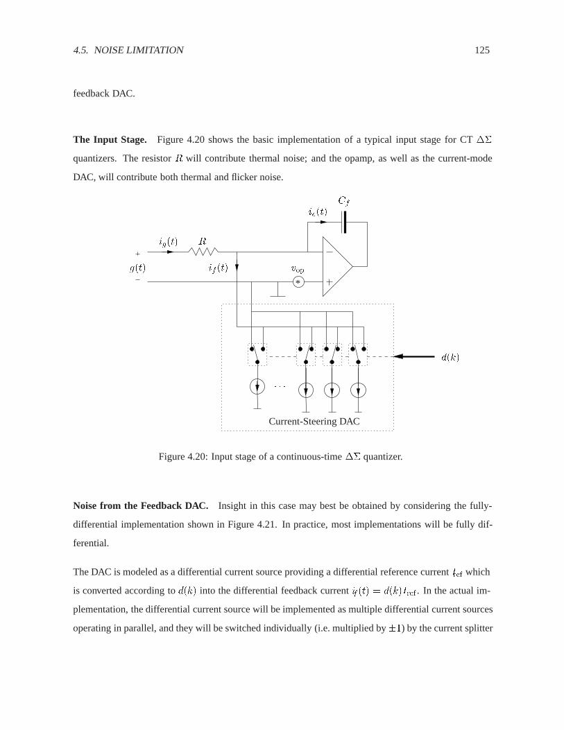
4.5. NOISE LIMITATION 125
feedback DAC.
The Input Stage. Figure 4.20 shows the basic implementation of a typical input stage for CT ��
quantizers. The resistor R will contribute thermal noise; and the opamp, as well as the current-mode
DAC, will contribute both thermal and flicker noise.
g(t)
ig(t)
� � �
Current-Steering DAC
ie(t)Cf
vopif (t)
d(k)
R
*
Figure 4.20: Input stage of a continuous-time �� quantizer.
Noise from the Feedback DAC. Insight in this case may best be obtained by considering the fully-
differential implementation shown in Figure 4.21. In practice, most implementations will be fully dif-
ferential.
The DAC is modeled as a differential current source providing a differential reference current Iref which
is converted according to d(k) into the differential feedback current if (t) = d(k)Iref . In the actual im-
plementation, the differential current source will be implemented as multiple differential current sources
operating in parallel, and they will be switched individually (i.e. multiplied by�1) by the current splitter
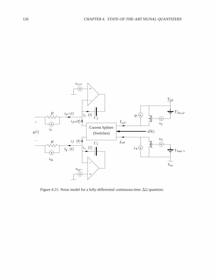
126 CHAPTER 4. STATE-OF-THE-ART SIGNAL QUANTIZERS
*
*
*
vop+
*
*
*
R
R
Cf
Cf
g(t)
Iref�if�(t)
if+(t)
Current Splitter
(Switches)
ie+(t)
ie�(t)
vN
Vss
Vdd
Vbias;N
vP
d(k)
Vbias;P
Iref+
*iP
iN *
vop�
ig�(t)
ig+(t)
ith�
ith+
Figure 4.21: Noise model for a fully-differential continuous-time �� quantizer.
4.5. NOISE LIMITATION 127
(cf. Figure 4.20). The operation can be described in the form
if+(t) + if�(t) = d(k)[Iref+ + Iref� ] (4.51)
if+(t)� if�(t) = Iref+ � Iref� (4.52)
Because the current splitter is merely an array of data-controlled switches, it will not produce noise.
Flicker noise is mainly caused by fluctuations in the current-source MOSFETs’ effective threshold volt-
age, and so it can be modeled by the gate-referred noise voltages vN and vP. When the flicker noise is
referred to the input g(t), it will become modulated by d(k) and magnified by R � gm, where gm is the
respective current source’s transconductance. Since the reference current is switched and not dumped,
the modulation by d(k) will not change the flicker noise’s power, but merely its spectral composition.
Hence the input-referred flicker noise can be calculated as
v icker;input;DAC =qv2Pg
2m;PR
2 + v2Ng2m;NR
2
= Rqv2Pg
2m;P + v2Ng
2m;N (4.53)
Because d(k) presumably will have most of its power in the signal band45, and because flicker noise has
a low bandwidth, v icker;input;DAC should be considered to be signal-band noise.
The total power of the flicker-noise voltages vN and vP can be controlled independently by changing the
transistor area while preserving the aspect ratio, therefore (for simplicity), the following discussion will
be based on the assumption that vN ' vP, and hence
v icker;input;DAC;inband = vN;P
hRqg2m;P + g2m;N
i(4.54)
The current sources’ thermal noise can (assuming strong inversion) be represented by the (signal-band)
noise currents
iN =p4kT�fgm;N (4.55)
iP =p4kT�fgm;P (4.56)
45Assuming that d(k) is the output from a multi-bit �� quantizer.
128 CHAPTER 4. STATE-OF-THE-ART SIGNAL QUANTIZERS
where �f is the width of the signal band. When referred to the input, the (signal band) thermal noise
voltage takes the form
vthermal;input;DAC;inband =p4kTR�f
hRq[g2m;N + g2m;P]
i(4.57)
Notice that both the flicker noise and the thermal noise (cf. (4.54) and (4.57)) are proportional to the
gain factor Rq[g2m;N + g2m;P], and hence the MOSFETs’ transconductance should be minimized.
The transconductances can be expressed as
gm;P =2Iref+
Ve�;Pwhere Ve�;P = Vbias;P � jVth;Pj (4.58)
gm;N =2Iref�
Ve�;Nwhere Ve�;N = Vbias;N � Vth;N (4.59)
To optimize the input signal swing while avoiding a common-mode component in the reference cur-
rents46, it is preferable that the opamps’ virtual ground potential be Vsupply=2, and hence (to keep the
MOSFETs operating in saturation) it is a requirement that47
Ve�;N � Vsupply=2 and Ve�;P � Vsupply=2 (4.60)
Because the reference current must be able to balance the input current, it follows that
Iref+ = Iref� �Vsupply2R
(4.61)
By combining the Equations (4.58) through (4.61) it can be shown that
Rq[g2m;N + g2m;P] > R
s�2
R
�2+
�2
R
�2=p8 (4.62)
and in conclusion, Equations (4.57) and (4.64) can be evaluated as
vthermal;input;DAC;inband �p4kTR�f
p8 (4.63)
v icker;input;DAC � vN;Pp8 (4.64)
46Preferable in order to minimize the transconductance (cf. Equations (4.58) and (4.59)).47The current-source MOSFETs will typically be cascode-coupled, and hence they can potentially be operated in the triode
region. However, to avoid an additional noise contribution from the cascode transistors, the output impedance of the current-
source MOSFETs should be reasonable high, i.e., they should be operated in saturation.
4.5. NOISE LIMITATION 129
Overall Thermal Noise Performance. For simplicity, assume that the opamps are designed to have an
equivalent thermal-noise resistance of approximately R. Because the opamp’s gain-bandwidth product
must be higher than the highest signal-band frequency, it follows that the opamps and the resistors will
have the same spectral power density 4kTR�f . The overall thermal-noise performance is therefore (cf.
(4.63))
Pinband;thermal;continuous;di�erential = 4kTR�f [8 + 1 + 1 + 1 + 1]
= 48kTR�f (4.65)
The result (4.65) will now be compared to the derived thermal-noise performance estimate (4.49) for DT
�� quantizers. Considering that the input capacitance Ci has an equivalent resistance of
Reqv =1
Cifs=
1
Ci � OSR � 2�f (4.66)
it follows that DT �� quantizers’ thermal-noise performance can be expressed as
Pthermal;inband;discrete = 10kTReqv�f (4.67)
which, for a differential implementation yields
Pthermal;inband;discrete;di�erential = 20kTReqv�f (4.68)
From this point of view, a DT �� quantizer’s thermal noise performance is approximately 4 dB better
than that of a CT �� quantizer. However, this conclusion is somewhat misleading, because generally
it will be possible (for the same power consumption and using the same technology) to choose the
physical resistor R significantly smaller than Reqv, therefore, CT �� quantizers can be designed to
have a better noise performance. This is especially true for low-frequency (audio) quantizers, where
R = 2048Reqv = 1 k would require Ci to be approximately 1 nF for �f = 20 kHz and OSR = 10. In
other words, assuming that OSR = 10 is sufficient to obtain the required SER performance, a DT ��
quantizer will have to be operated at a much higher OSR (in the order of 1000) using practical capacitors
to obtain the SNR performance of a CT �� quantizer with R = 1 k. Hence, the CT �� quantizer is
highly preferable from a power-consumption point of view. Even when the bandwidth is so large that
the same OSR is required, the CT �� quantizer can be designed to have a lower power consumption,
because the opamps are not subject to the same high requirements.

130 CHAPTER 4. STATE-OF-THE-ART SIGNAL QUANTIZERS
To get a better feeling for the numbers quoted, it may be interesting to note that for R = 1 k and
�f = 1 MHz, the signal-band thermal noise of a CT �� quantizer is �97 dBV, and hence for a 5 V
supply voltage 108 dB SNR is within reach.
As a verification of the evaluations made above, one may compare them to the measurements made
for the design presented in [35]. The bandwidth was 20 kHz and the resistors were designed with a
nominal resistance of 1.8 k. The PMOS current source was not switched, which implies that the gain
factor (4.62) is doubled, and hence that 10 log10(36=12) dB = 4:8 dB more noise than predicted by
the above estimate is to be expected. Assuming that the full-scale output swing was defined as �5Vpp(for the differential circuit operating on a 5 V supply voltage), the above estimate predicts the SNR
performance to be no better than 117 dB. The actual SNR performance measured was 113 dB. The small
4 dB difference is very realistic for a good design, considering that the measured SNR also includes
flicker noise, quantization noise, clock-jitter-induced noise, etc., and that the current sources probably
were not designed quite as aggressively as assumed in (4.60).
Overall Flicker Noise Performance. The flicker noise component is hard to estimate accurately, be-
cause it depends highly on the technology used for the implementation of the circuit. The following
calculations are based on measurements48 for a 3 �m technology, for which the gate-referred noise volt-
age is estimated to be approximately 300 [nV=p
Hz]@10 Hz for a 1500 �m2 transistor of either polarity.
However, because flicker noise voltage is believed to be proportional to the gate oxide’s thickness, less
flicker noise can be expected when using a modern sub-micron technology.
Assuming that the lowest frequency of interest is flow, the gate-referred flicker noise voltage for the
48Performed by Dr. Christian Enz and provided in his lecture notes from a short course on low-noise amplifiers at EPFL in
Lausanne, Switzerland, August 1996.

4.5. NOISE LIMITATION 131
considered technology can be calculated (for �f � flow) from
v icker;MOS =
s(300 � 10�9V)21500�m2
W � LZ �f
flow
10
fdf
=
s10(300 � 10�9V)21500�m2
W � L ln
��f
flow
�
' 1�V
r1500�m2
W � L
sln
��f
flow
�(4.69)
An opamps’ input-referred flicker noise depends on the topology in which it is implemented; but assume
(for simplicity) that four equally-sized (and equal-transconductance) transistors contribute to vop. In this
case, the opamps’ input-referred flicker noise can be evaluated as
v icker;opamp;input ' 2:8�V
s1500�m2
Wopamp � Lopamp
sln
��f
flow
�(4.70)
The DAC’s flicker noise contribution will be (cf. (4.64))
v icker;input;DAC ' 2:8�V
s1500�m2
WDAC � LDAC
sln
��f
flow
�(4.71)
To obtain the required degree of matching, the DAC’s current sources will typically be implemented on
a much larger chip area than that of the opamps’ input differential pair; consequently, the overall flicker
noise performance can be estimated roughly as
v icker;input ' v icker;input;opamp ' 2:8�V
s1500�m2
Wopamp � Lopamp
sln
��f
flow
�(4.72)
For flow = 10 Hz, �f = 1 MHz, and a transistor area of 1500�m2, the input-referred flicker noise will
be approximately �100 dBV, which implies that the flicker noise (in this situation) is dominated by
the thermal noise, even when the input resistor R is as small as 1 k. Considering that the gate-oxide
thickness (and hence the flicker-noise coefficient) is a decreasing function of the technology’s minimum
feature size, it follows that good flicker-noise performance can be obtained with a modern sub-micron
technology, even when using transistors of a more moderate size (10 �m2).

132 CHAPTER 4. STATE-OF-THE-ART SIGNAL QUANTIZERS
4.5.3 Conclusion
Continuous-time systems generally have a better thermal noise performance than discrete-time systems
because the sampling also causes aliasing of the broadband noise, whereby the signal-band noise power
increases. Quantizers always have a discrete-time (digital) output signal; but, as discussed above, the
impact of noise aliasing depends highly on where the sampling is performed. CT �� quantizers sample
the signal in the last stage of the (high-gain) closed-loop structure, and hence aliasing errors are effi-
ciently suppressed. CT �� quantizers can be made so robust with respect to aliasing errors that not only
noise aliasing but also signal aliasing is tolerable. In other words, a separate anti-aliasing filter is not
required.
Because the noise performance of CT �� quantizers is limited mainly by the noise from the feedback
DAC, and because they can be designed to have a low power consumption, these quantizers will probably
dominate the market if and when (cf. Chapter 5) the industry learns to design highly-linear current-mode
DACs.
This section has only considered device noise, i.e., thermal and flicker noise; but a different kind of noise
– substrate noise – is usually the main problem in mixed-mode circuits, which become ever more impor-
tant, and which usually require high-performance A/D and D/A converters in the analog portion of the
circuit. In these circuits, high-resolution discrete-time analog signals simply cannot be allowed because
the digital-switching noise’s high-power high-frequency spectral components alias into the signal band
in the sampling process. For the above reasons, CT �� quantizers may represent the only way by which
high-resolution quantizers can be implemented.

Chapter 5
Improved Current-Mode DACs
In Chapter 4, it was discussed that CT �� quantizers have several advantages compared to DT ��
quantizers in terms of speed, power consumption, and noise performance. However, as discussed in
Section 3.2.2, dynamic errors from the feedback DAC is the main obstacle that prevents the successful
design of high-performance CT�� quantizers. It is well understood that intersymbol-interference errors
(cf. page 47) generally are the main source of distortion, but also that return-to-zero (RTZ) switching (cf.
page 48) can suppress these errors to a very low level. Unfortunately, the (classic) RTZ switching scheme
is associated with an increased sensitivity to clock-jitter-induced noise (cf. page 52), which makes it
nearly impossible to implement commercial high-resolution wide-bandwidth DACs. This chapter will
discuss techniques for the implementation of current-mode DACs, which are robust with respect to both
intersymbol-interference and clock-jitter-induced errors. The best technique proposed will also avoid
the timing and nonlinear-switching errors discussed on page 46.
5.1 Dual Return-to-Zero Current-Mode DAC
The RTZ switching scheme represents a good school of thought in that it relies neither on matching
of nor the absolute value of electrical parameters. However, it does rely on the ability to accurately
133
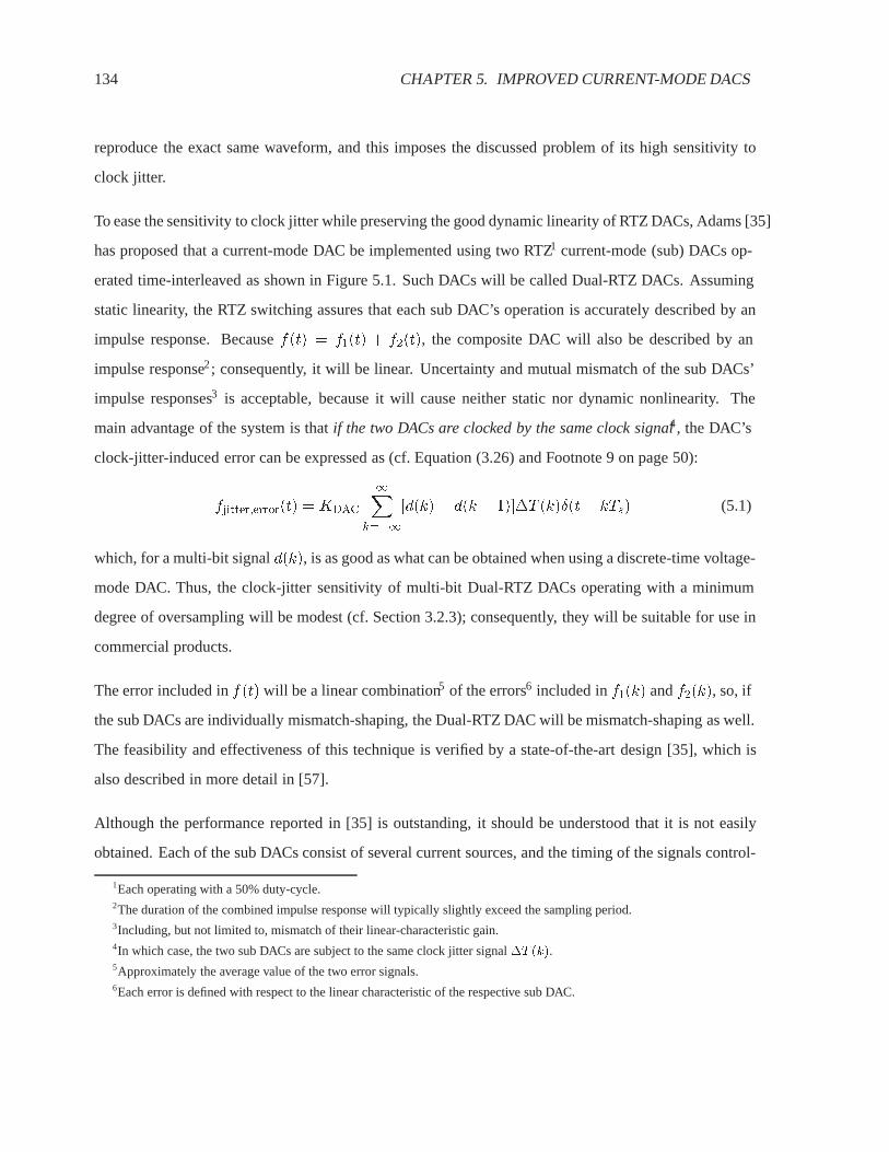
134 CHAPTER 5. IMPROVED CURRENT-MODE DACS
reproduce the exact same waveform, and this imposes the discussed problem of its high sensitivity to
clock jitter.
To ease the sensitivity to clock jitter while preserving the good dynamic linearity of RTZ DACs, Adams [35]
has proposed that a current-mode DAC be implemented using two RTZ1 current-mode (sub) DACs op-
erated time-interleaved as shown in Figure 5.1. Such DACs will be called Dual-RTZ DACs. Assuming
static linearity, the RTZ switching assures that each sub DAC’s operation is accurately described by an
impulse response. Because f(t) = f1(t) + f2(t), the composite DAC will also be described by an
impulse response2; consequently, it will be linear. Uncertainty and mutual mismatch of the sub DACs’
impulse responses3 is acceptable, because it will cause neither static nor dynamic nonlinearity. The
main advantage of the system is that if the two DACs are clocked by the same clock signal4, the DAC’s
clock-jitter-induced error can be expressed as (cf. Equation (3.26) and Footnote 9 on page 50):
fjitter;error(t) = KDAC
1Xk=�1
[d(k) � d(k � 1)]�T (k)Æ(t � kTs) (5.1)
which, for a multi-bit signal d(k), is as good as what can be obtained when using a discrete-time voltage-
mode DAC. Thus, the clock-jitter sensitivity of multi-bit Dual-RTZ DACs operating with a minimum
degree of oversampling will be modest (cf. Section 3.2.3); consequently, they will be suitable for use in
commercial products.
The error included in f(t) will be a linear combination5 of the errors6 included in f1(k) and f2(k), so, if
the sub DACs are individually mismatch-shaping, the Dual-RTZ DAC will be mismatch-shaping as well.
The feasibility and effectiveness of this technique is verified by a state-of-the-art design [35], which is
also described in more detail in [57].
Although the performance reported in [35] is outstanding, it should be understood that it is not easily
obtained. Each of the sub DACs consist of several current sources, and the timing of the signals control-
1Each operating with a 50% duty-cycle.2The duration of the combined impulse response will typically slightly exceed the sampling period.3Including, but not limited to, mismatch of their linear-characteristic gain.4In which case, the two sub DACs are subject to the same clock jitter signal �T (k).5Approximately the average value of the two error signals.6Each error is defined with respect to the linear characteristic of the respective sub DAC.
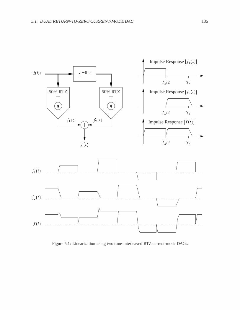
5.1. DUAL RETURN-TO-ZERO CURRENT-MODE DAC 135
f(t)
f1(t) f2(t)
z�0:5
50% RTZ 50% RTZ
Ts
Ts
TsTs/2
Ts/2
Ts/2
Impulse Response [f1(t)]
Impulse Response [f2(t)]
Impulse Response [f(t)]
f1(t)
f2(t)
f(t)
d(k)
Figure 5.1: Linearization using two time-interleaved RTZ current-mode DACs.

136 CHAPTER 5. IMPROVED CURRENT-MODE DACS
ling these many current sources must be synchronized not only within each sub DAC, but also mutually
between the two sub DACs. In other words, the success of the design depends significantly on the ex-
perience of the actual designer(s) and layout person(s), because timing errors and nonlinear switching
errors are still major concerns (cf. page 46).
5.1.1 A Variation
The fundamental element in the RTZ switching scheme is that no current source is used in any two
samples without being brought to a fixed status (the “zero” in “return-to-zero”) in between. When
used in combination with mismatch-shaping techniques, reduced clock-jitter sensitivity can be obtained
without using the Dual-RTZ switching scheme.
First notice that the fundamental property of the element-rotation mismatch-shaping encoder is that,
with respect to any origin in time, no unit element is used twice before the other unit elements have
been used in between. Hence, if an ERS UE-MS DAC is implemented with twice as many unit-element
current sources as the maximum code to be D/A converted, it follows that the encoder will automatically
perform RTZ switching7. The advantage of this approach in comparison to the Dual-RTZ switching
scheme is that the currents are switched at half the frequency, therefore, timing errors and nonlinear
switching errors are suppressed by 3 dB.
5.2 Time-Interleaved Current-Mode DAC
This section will describe a simple technique for the implementation of current-mode DACs with a
very good dynamic linearity/performance. As for Dual-RTZ DACs, the output current is generated by
switching between two (or more) DACs, but dynamic linearity is obtained using another technique not
employing RTZ switching.
Dynamic nonlinearity is avoided by operating two DACs time interleaved, and by connecting the DACs
to the output only after they have settled from being updated. Thereby, all switching effects become
7It is assumed that each unit-element current source operates with a 100% duty cycle.

5.2. TIME-INTERLEAVED CURRENT-MODE DAC 137
invisible seen from the output terminal. The switching between the two DACs is performed at one
centralized node, whereby the DAC becomes as insensitive to clock-jitter as Dual-RTZ DACs, but it is
also insensitive to nonlinear-switching, intersymbol-interference, and timing errors. Hence, the proposed
technique is useful not only for the implementation of high-performance oversampled data converters,
but also for high-speed DACs with bandwidths of, say, 100 MHz or more.
5.2.1 Basic Topology and Operation
Figure 5.2 shows the basic implementation of the proposed DAC structure. DAC 1 receives the new
input value d(k) slightly after the onset of �2, whereas DAC 2 receives it half a sampling period later
(slightly after the onset of �1). The switching block consisting of the four PMOS transistors is controlled
such that the output f1(t) from DAC 1 is connected to the output, i.e., f(t) = f1(t) in clock phases �1,
whereas the output f2(t) from DAC 2 is connected to the output, i.e., f(t) = f2(t) in clock phases �2.
The point is that when the DACs are updated, the respective DAC is connected to a through-away
point (i.e., the current is dumped to an arbitrary low-impedance terminal, preferably having the same
virtual-ground potential as the load terminal), and the potential switching errors – including timing,
intersymbol-interference, and nonlinear-switching errors – will not affect the output signal f(t) in any
way. The only requirement is that when the DACs are updated, they must settle to their static value
within approximately half a sampling period, at which point they are connected to the output terminal.
The four PMOS transistors constituting the switching block may either be operated as CMOS switches,
in which case the two active transistors operate in their triode region, or as hard-driven differential pairs,
in which case the two active transistors operate in their saturation region. Either way, it is imperative
that the differential driver is implemented such that the switching block implements a make-before-
break switching function. Such differential drivers are well known and widely used (see [58]). For the
implementation of high-speed DACs, the switching block may be driven such that all four transistors
always are active and operate in saturation, and such that only one transistor of each differential pair
carries the majority (say 99%) of the tail current fx(t).
138 CHAPTER 5. IMPROVED CURRENT-MODE DACS
�1
�2
S
Q
R
D Dd(k)
�2d �1d
DAC 2DAC 1
f(t)
f2(t)f1(t)
�2 �2 �2 �2 �2 �1�1�1�1�1�1
Differential Driver
f(t)
f2(t)
f1(t)
Figure 5.2: Basic topology of the time-interleaved current-mode DAC.
5.2. TIME-INTERLEAVED CURRENT-MODE DAC 139
5.2.2 Analysis
Whereas deleterious dynamic effects associated with the update of each DAC are efficiently prevented,
the switching block can potentially cause switching errors. The situation is, however, much improved
compared to stand-alone current-mode DACs as well as Dual-RTZ DACs.
Timing errors will obviously not be a problem. The mere fact that the switching function is centralized
assures that all current sources in each DAC are updated at exactly the same instance with respect to f(t).
Glitches may occur in the transition from one clock phase to the next, but assuming that the differential
driver provides a consistent switching waveform8, these glitches will be linearly related to the input
signal d(k), and hence they do not pose a problem.
Nonlinear-switching errors9 can occur if the switching waveform provided by the differential driver
is not consistent. Consistency is, however, reasonably simple to obtain because it refers to only one
signal, and any reminiscence of the potential nonlinear error can be suppressed efficiently by making the
differential driver fast. Notice that only the differential driver and the switching block “need” to be fast;
the two sub DACs may be significantly slower (as shown in Figure 5.2), and that is a property which can
be used to minimize the digital circuit elements’ power consumption (of concern in high-speed DACs).
Charge injection can sometimes cause nonlinear-switching errors, but this implementation is indeed very
robust with respect to charge-injection errors. If the active PMOS transistors are operated in saturation,
the charge-injection signal will be proportional to the switched signal, because the inversion charge of
a saturated MOSFET is proportional to the conducted current, and hence it is a linear effect. On the
other hand, if the active PMOS transistors are operated in the triode region, the charge-injection signal
will be independent of the switched signal because the opamp provides a virtual ground, and hence the
8Any waveform is acceptable because linearity is dependent on repeatability only. “Switching waveform” refers to the
provided waveform locally around (i.e. from shortly before to shortly after) the switching instances, and hence it is independent
of clock jitter. It is acceptable if the switching waveform �1 ! �2 differs from the switching waveform �2 ! �1, as long as
they are consistent individually.9This type of error should more precisely be considered to be noise rather than nonlinear errors. It can be assured that
the differential driver is not affected by the signal d(k), and hence the error will not be deterministically related to the signal
(which is the fundamental property of nonlinear errors).

140 CHAPTER 5. IMPROVED CURRENT-MODE DACS
gate-to-channel potential will be constant. This is also a linear effect.
Conclusion. The proposed time-interleaved DACs are characterized by the same advantages as the
Dual-RTZ DACs, namely reduced clock-jitter sensitivity, insensitivity to mismatch of the sub DACs’
gain and offset, and that a time-interleaved DAC will be mismatch-shaping if the sub DACs are individ-
ually mismatch-shaping10. However, as discussed above, time-interleaved DACs are also characterized
by an improved immunity to timing errors as well as nonlinear-switching errors, and hence they are
much less critical to implement, compared to Dual-RTZ DACs, for example. The improved robustness
can be used constructively to reduce the overall chip area, or to employ more modular layout techniques,
which potentially can help reduce a product’s turn-around time.
In conclusion, time-interleaved current-mode DACs are very suitable for use in commercial products,
whether they are high-speed, high-performance, or short-design-time applications.
5.3 Conclusion
The successful implementation [35] of a mismatch-shaping Dual-RTZ DAC has verified that it is fea-
sible to implement current-mode DACs with a very good dynamic performance. The proposed time-
interleaved DACs represent an improved concept, which combines the advantages of Dual-RTZ DACs
with insensitivity to timing errors, thereby providing an even more robust architecture for the implemen-
tation of current-mode DACs.
10The property that the time-interleaved DAC’s error signal is the average value of the sub DACs’ error signals implies that
the requirement of two (or more) sub DACs need not imply that the time-interleaved DAC will require twice the chip area
for its implementation (compared to a stand-alone DAC of the same static linearity). A DAC will occupy a minimum area A
which cannot be reduced because the area is related to the stochastic element in the technology’s matching properties. To avoid
systematic errors, the minimum area A is often divided into (say) two areas A1 and A2 of equal size, and chosen according to
the common-centroid layout principle (cf. page 59). It is easily identified that if DAC 1 is laid out on A1, and DAC 2 is laid
out (symmetrically) on A2, the composite DAC will fulfill the common-centroid principle even if the individual DACs do not.
In other words, in terms of stochastic properties, time averaging is equivalent to coordinate averaging, and hence the total area
A = A1 [ A2 can be the same as if only one DAC had been implemented.

5.3. CONCLUSION 141
High-performance current-mode DACs are, in general, more difficult to implement than discrete-time
voltage-mode DACs. However, in critical design situations (low-power, low-noise, or high-speed) the
extra difficulty may well be worth the trouble because the achievable improvement in performance can
be as much as a factor of 10.

142 CHAPTER 5. IMPROVED CURRENT-MODE DACS

Chapter 6
Dithering of Mismatch-Shaping DACs
Unit-element mismatch-shaping (UE-MS) DACs are by themselves important circuits, and they are also
important for the implementation of scaled-element mismatch-shaping DACs which are discussed in
Chapter 7. Unfortunately (as discussed in Section 4.4.3), UE-MS DACs have a tendency to produce idle
tones1 that can ruin the performance of an otherwise well designed data converter [51].
Fortunately, idle tones can be prevented using dithering techniques. This chapter will discuss and analyze
a prior-art dithering technique dedicated for tree-structure UE-MS encoders, and two novel dithering
techniques for use with the simpler ERS encoders will be proposed. As discussed in Section 4.4.5, first-
order UE-MS DACs are usually preferable2 in comparison to higher-order UE-MS DACs; hence, the
discussion will center around only first-order encoders.
6.1 Idle Tones in Deterministic UE-MS Encoders
Idle tones in mismatch-shaping DACs are caused by periodic/systematic use of the unit elements. The
following discussion will consider the idle-tone behavior of deterministic UE-MS encoders, i.e., en-
1Spurious tones caused by periodic use/shuffling of the unit elements.2In terms of simplicity, but also in terms of performance for OSR less than 25.
143

144 CHAPTER 6. DITHERING OF MISMATCH-SHAPING DACS
coders in which the unit elements for the conversion of d(k) are selected as a function of only the signal
d(k) and an initial condition. These encoders represent the majority of the published/known encoders.
6.1.1 Idle Tones in ERS UE-MS Encoders
Element-Rotation-Scheme (ERS) UE-MS encoders select the unit elements for the D/A conversion of
d(k) according to the very simple rotation rule described on page 103, and hence they have a tendency
to produce idle tones (cf. page 105). The following discussion refers to Figures 4.9 and 4.10.
Assume that the input d(k) is periodic with the minimum period P . A certain number
Q =PXi=1
d(i) (6.1)
of elements will be used for the conversion of one period of d(k).
Considering the nature of the ERS algorithm, it follows that the conversion of one period of d(k) is
characterized by a certain increment (modulo N , where N is the number of unit elements) of the rotation
pointer r(k)
r(k + P ) = modulo[r(k) +Q;N ] (6.2)
The rotation pointer r(k) will be periodic signal with a period of NP samples (and possibly also with a
shorter period)
r(k +NP ) = modulo[r(k) +NQ;N ] = modulo[r(k); N ] = r(k) (6.3)
Because the signal d(k) and the rotation pointer r(k) are periodic with the same period NP , the use
of the unit elements (and hence the error signal m(k)) will be periodic with the period NP as well.
Consequently, the error signal m(k) will consist of only idle tones, which are located at integer multiples
of the frequency fs=(NP ).
Performance Evaluation. The above analysis indicates that the ERS encoder is indeed very likely to
produce idle tones, and that there is no reason to believe that they will not appear in the signal band.
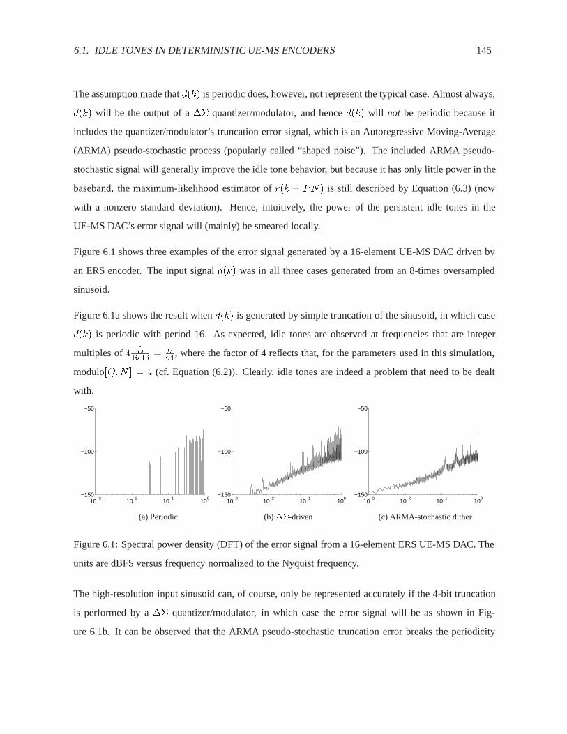
6.1. IDLE TONES IN DETERMINISTIC UE-MS ENCODERS 145
The assumption made that d(k) is periodic does, however, not represent the typical case. Almost always,
d(k) will be the output of a �� quantizer/modulator, and hence d(k) will not be periodic because it
includes the quantizer/modulator’s truncation error signal, which is an Autoregressive Moving-Average
(ARMA) pseudo-stochastic process (popularly called “shaped noise”). The included ARMA pseudo-
stochastic signal will generally improve the idle tone behavior, but because it has only little power in the
baseband, the maximum-likelihood estimator of r(k + PN) is still described by Equation (6.3) (now
with a nonzero standard deviation). Hence, intuitively, the power of the persistent idle tones in the
UE-MS DAC’s error signal will (mainly) be smeared locally.
Figure 6.1 shows three examples of the error signal generated by a 16-element UE-MS DAC driven by
an ERS encoder. The input signal d(k) was in all three cases generated from an 8-times oversampled
sinusoid.
Figure 6.1a shows the result when d(k) is generated by simple truncation of the sinusoid, in which case
d(k) is periodic with period 16. As expected, idle tones are observed at frequencies that are integer
multiples of 4 fs16�16 = fs
64 , where the factor of 4 reflects that, for the parameters used in this simulation,
modulo[Q;N ] = 4 (cf. Equation (6.2)). Clearly, idle tones are indeed a problem that need to be dealt
with.
10−3
10−2
10−1
100
−150
−100
−50
10−3
10−2
10−1
100
−150
−100
−50
10−3
10−2
10−1
100
−150
−100
−50
(b) ��-driven (c) ARMA-stochastic dither(a) Periodic
Figure 6.1: Spectral power density (DFT) of the error signal from a 16-element ERS UE-MS DAC. The
units are dBFS versus frequency normalized to the Nyquist frequency.
The high-resolution input sinusoid can, of course, only be represented accurately if the 4-bit truncation
is performed by a �� quantizer/modulator, in which case the error signal will be as shown in Fig-
ure 6.1b. It can be observed that the ARMA pseudo-stochastic truncation error breaks the periodicity

146 CHAPTER 6. DITHERING OF MISMATCH-SHAPING DACS
and thereby spreads the error signal’s power to, presumably, all frequencies, but idle tones are still a ma-
jor problem. Notice that the ARMA pseudo-stochastic truncation error does not spread the error signal’s
spectral power density as predicted above, but that idle tones rather appear at discrete frequencies in an
unpredictable pattern. The discrepancy reflects the “pseudo” in the ARMA pseudo-stochastic truncation
error, i.e., that the truncation error is correlated with the sinusoid, and hence does not originate from
a truly stochastic process. To support and investigate the validity this explanation, a third simulation
was performed where d(k) was generated by truncating the sinusoid (as in Figure 6.1a) and adding to it
the output from an independent �� modulator with zero input achieving a realistic non-pseudo ARMA
stochastic process. The spectral power density of the error signal produced in this way is shown in
Figure 6.1(c). Now, the expected local spreading of the persistent idle tones can be observed.
Conclusion. Figure 6.1b shows the spectral power density of a typical-case error signal m(k) gener-
ated by a UE-MS DAC driven by an ERS encoder (Figures 6.1a and 6.1c do not correspond to useful
systems). Strong idle tones are observed, and they should be expected whenever the simple ERS encoder
is used. The performance is unacceptable for a wide range of applications, and hence better UE-MS en-
coders are needed.
6.1.2 Idle Tones in Complex UE-MS Encoders
It is often claimed – and there is some truth to it – that the idle-tone behavior can be improved by
selecting the unit elements in a pattern which is more “complex” than the simple rotation pattern used
by the ERS encoders. Several techniques have been proposed [9] [14] [39], but neither of them is
actually recommendable unless a stochastic element3 (dither) is appropriately incorporated. Indeed, idle
tones are less likely to occur when using these encoders, but as long as the encoders are deterministic
digital state machines, idle tones can (and usually do) exist. The problem is that the idle tones may
be so hard to find (by means of time-consuming and therefore sparse simulations) that the designer is
3Truly stochastic processes cannot be implemented using only digital circuitry, but a pseudo-random process is in general
sufficient for all practical purposes. By assuring that the pseudo-random sequence has a sufficiently long (minimum) period,
the resultant idle tones can be made arbitrarily dense in frequency.
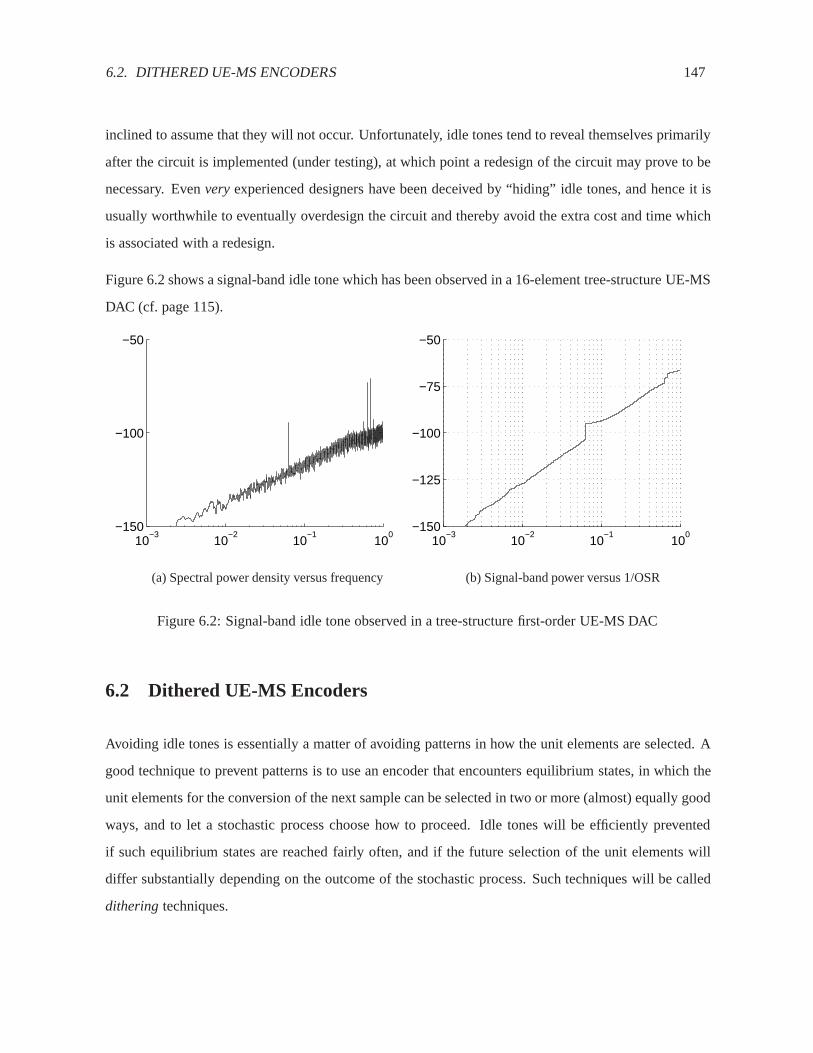
6.2. DITHERED UE-MS ENCODERS 147
inclined to assume that they will not occur. Unfortunately, idle tones tend to reveal themselves primarily
after the circuit is implemented (under testing), at which point a redesign of the circuit may prove to be
necessary. Even very experienced designers have been deceived by “hiding” idle tones, and hence it is
usually worthwhile to eventually overdesign the circuit and thereby avoid the extra cost and time which
is associated with a redesign.
Figure 6.2 shows a signal-band idle tone which has been observed in a 16-element tree-structure UE-MS
DAC (cf. page 115).
10−3
10−2
10−1
100
−150
−125
−100
−75
−50
10−3
10−2
10−1
100
−150
−100
−50
(a) Spectral power density versus frequency (b) Signal-band power versus 1/OSR
Figure 6.2: Signal-band idle tone observed in a tree-structure first-order UE-MS DAC
6.2 Dithered UE-MS Encoders
Avoiding idle tones is essentially a matter of avoiding patterns in how the unit elements are selected. A
good technique to prevent patterns is to use an encoder that encounters equilibrium states, in which the
unit elements for the conversion of the next sample can be selected in two or more (almost) equally good
ways, and to let a stochastic process choose how to proceed. Idle tones will be efficiently prevented
if such equilibrium states are reached fairly often, and if the future selection of the unit elements will
differ substantially depending on the outcome of the stochastic process. Such techniques will be called
dithering techniques.
148 CHAPTER 6. DITHERING OF MISMATCH-SHAPING DACS
6.2.1 Dithered Tree-Structure UE-MS Encoders
Tree-structure UE-MS encoders were discussed in Section 4.4.4, and a specific first-order implemen-
tation was discussed on page 115. The overall operation relies on the operation of the node separa-
tors, which must each generate a signal t(k) of values f�1; 0; 1g such that the sum jPki=1 t(i)j is
bounded/minimized for all k. Whenever a node separator receives an odd signal, t(k) must be chosen
as �1, otherwise as 0. Obviously, t(k) should always be chosen of the opposite polarity as that ofPk�1i=1 t(i); but when the sum is zero, any choice may be equally good (i.e., its an equilibrium state).
Hence, dithering a tree-structure UE-MS encoder is a matter of, in all the node separators4, randomly
choosing the polarity of t(k) whenPk�1
i=1 t(i) = 0.
Figure 6.3 shows the characteristics of the error signal that was generated by a 16-element fully-dithered
tree-structure first-order UE-MS DAC when the input signal d(k) is a �12 dBFS 64-times oversampled
��-quantized sinusoid.
The dithering technique (which was first proposed in [14]) appears to be very efficient, but in Figure 6.2a
it is observed that the error signal’s spectral power density flattens around the Nyquist frequency. This
is not a major problem, but it does imply that the signal-band performance is less than what it perhaps
could be (compare Figures 6.2b and 4.17). The slight degradation is caused by a combination of two
effects:
1. In the dithered tree-structure encoder,Pk
i=1 t(i) will oscillate between the three values f-1,0,1ginstead of only the two values used by the deterministic encoder. Because the frequency of
jt(k)j = 1 events is the same, the dithered encoder will need more samples to correct for pre-
vious errors, and so it will not perform as well at high frequencies.
2. Midscale input d(k) (i.e., when half the unit elements are selected in each sample) is the optimum
operating condition for the encoder. This is because midscale input corresponds to the highest
4To efficiently avoid idle tones, a separate random bit should be generated for each node separator because idle tones have
been observed when the same stochastic process is shared by all the node separators. This observation supports the second rule
for how to obtain efficient dithering (cf. the introduction to this chapter), namely that the stochastic process must be allowed to
choose among substantially different patterns in the use of the unit elements.
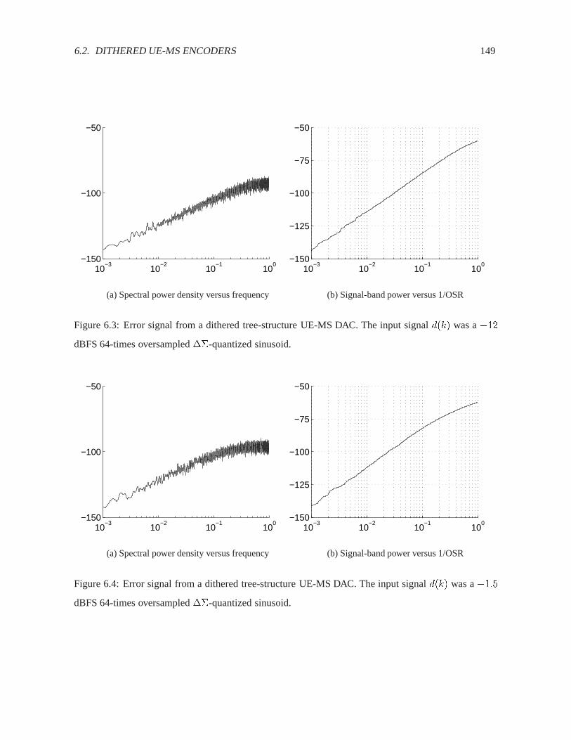
6.2. DITHERED UE-MS ENCODERS 149
10−3
10−2
10−1
100
−150
−125
−100
−75
−50
10−3
10−2
10−1
100
−150
−100
−50
(a) Spectral power density versus frequency (b) Signal-band power versus 1/OSR
Figure 6.3: Error signal from a dithered tree-structure UE-MS DAC. The input signal d(k) was a �12dBFS 64-times oversampled ��-quantized sinusoid.
10−3
10−2
10−1
100
−150
−125
−100
−75
−50
10−3
10−2
10−1
100
−150
−100
−50
(a) Spectral power density versus frequency (b) Signal-band power versus 1/OSR
Figure 6.4: Error signal from a dithered tree-structure UE-MS DAC. The input signal d(k) was a �1:5dBFS 64-times oversampled ��-quantized sinusoid.

150 CHAPTER 6. DITHERING OF MISMATCH-SHAPING DACS
probability (p = 0:5) for jt(k)j = 1 events, which is proportional to the closed-loop’s feedback
factor and thereby also the error signal’s controllability (cf. the discussion on page 115). If the
input signal includes long sequences for which nearly all/no unit elements are used, the error
signal’s controllability will deteriorate (in those periods), and hence the encoder’s high-frequency
performance will be degraded. Such sequences will be called low-control sequences. Low-control
sequences are, e.g., a characteristic of highly-oversampled full-scale sinusoid input signals. This
effect is dominating in Figure 6.4, where the magnitude of the ��-quantized sinusoid input signal
is increased to �1:5 dB full scale.
Low-Control Sequences. The following will study the effect of low-control sequences. For simplicity,gd(k) is defined as d(k) scaled such that a full-scale gd(k) spans the range from �1 to +1.
For a constant input d(k), each node separator in a tree-structure UE-MS encoder will (for each sample)
have a constant probability p = 1�jgd(k)j2 for jt(k)j = 1. The probability p is proportional to the control
system’s loop gain (cf. Figure 4.15 with a first-order loop filter), and hence the transfer function of the
filtering process to which the error signal is subject can be estimated as (for some empiric constant
a 2 R)
HMS(f) =1
1 + ap z�1
1+z�1
=1� z�1
1 + (ap� 1)z�1where z = ej2�f=fs (6.4)
In Equation 4.22 it was estimated that the error signal’s power density is related togd(k) aspp(1� p),
and hence – for all constant inputs d(k) – the spectral power density can presumably be expressed as
PSD(f) / 1� z�1
1 + (ap� 1)z�1
pp(1� p) where z = ej2�f=fs (6.5)
To investigate the validity and accuracy of Equation (6.5), a fully-dithered 16-element tree-structure
UE-MS DAC was simulated for 8 constant inputs, for which 8; 9; 10; : : : ; 15 unit elements were used
in average5. The signal-band power of the obtained error signals versus 1=OSR is shown in Figure 6.5
5As usual, the UE-MS DAC was driven by a �� modulator, and hence the neighbor values were used in a small fraction
of the time. This was mainly done to conform with the subsequent simulations, where a small amount of noise is required.
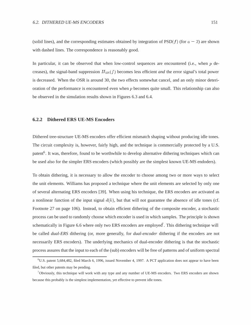
6.2. DITHERED UE-MS ENCODERS 151
(solid lines), and the corresponding estimates obtained by integration of PSD(f) (for a = 2) are shown
with dashed lines. The correspondence is reasonably good.
In particular, it can be observed that when low-control sequences are encountered (i.e., when p de-
creases), the signal-band suppression HMS(f) becomes less efficient and the error signal’s total power
is decreased. When the OSR is around 30, the two effects somewhat cancel, and an only minor deteri-
oration of the performance is encountered even when p becomes quite small. This relationship can also
be observed in the simulation results shown in Figures 6.3 and 6.4.
6.2.2 Dithered ERS UE-MS Encoders
Dithered tree-structure UE-MS encoders offer efficient mismatch shaping without producing idle tones.
The circuit complexity is, however, fairly high, and the technique is commercially protected by a U.S.
patent6. It was, therefore, found to be worthwhile to develop alternative dithering techniques which can
be used also for the simpler ERS encoders (which possibly are the simplest known UE-MS endoders).
To obtain dithering, it is necessary to allow the encoder to choose among two or more ways to select
the unit elements. Williams has proposed a technique where the unit elements are selected by only one
of several alternating ERS encoders [39]. When using his technique, the ERS encoders are activated as
a nonlinear function of the input signal d(k), but that will not guarantee the absence of idle tones (cf.
Footnote 27 on page 106). Instead, to obtain efficient dithering of the composite encoder, a stochastic
process can be used to randomly choose which encoder is used in which samples. The principle is shown
schematically in Figure 6.6 where only two ERS encoders are employed7. This dithering technique will
be called dual-ERS dithering (or, more generally, for dual-encoder dithering if the encoders are not
necessarily ERS encoders). The underlying mechanics of dual-encoder dithering is that the stochastic
process assures that the input to each of the (sub) encoders will be free of patterns and of uniform spectral
6U.S. patent 5,684,482, filed March 6, 1996, issued November 4, 1997. A PCT application does not appear to have been
filed, but other patents may be pending.7Obviously, this technique will work with any type and any number of UE-MS encoders. Two ERS encoders are shown
because this probably is the simplest implementation, yet effective to prevent idle tones.
152 CHAPTER 6. DITHERING OF MISMATCH-SHAPING DACS
10−3
10−2
10−1
100
−150
−125
−100
−75
−50
10−3
10−2
10−1
100
−150
−125
−100
−75
−50
10−3
10−2
10−1
100
−150
−125
−100
−75
−50
10−3
10−2
10−1
100
−150
−125
−100
−75
−50
10−3
10−2
10−1
100
−150
−125
−100
−75
−50
10−3
10−2
10−1
100
−150
−125
−100
−75
−50
10−3
10−2
10−1
100
−150
−125
−100
−75
−50
10−3
10−2
10−1
100
−150
−125
−100
−75
−50
p = 7=16
p = 5=16
p = 3=16
p = 1=16p = 2=16
p = 4=16
p = 6=16
p = 8=16
Figure 6.5: Static performance of a dithered tree-structure UE-MS encoder. The plots show the signal-
band power versus 1/OSR for each constant value of d(k).

6.2. DITHERED UE-MS ENCODERS 153
power density. It is simple to show that the mismatch-shaping property is preserved (provided that only
one set of unit elements is used).
UE-DACRandom Processd(k) f(k)
ERS
ERS
Encoder
Encoder
Figure 6.6: Basic principle for a dithered ERS encoder
Simulation Results and Evaluation. The dynamic performance of a dual-ERS dithered UE-MS en-
coder is illustrated in part by Figures 6.7 and 6.8, which correspond to Figures 6.3 and 6.4, respectively,
in that they are based on the same operating conditions. The performance is quite similar to that of fully
dithered tree-structure UE-MS encoders.
The mismatch-shaping property of ERS encoders is obtained because the error cancels every time the
rotation pointer wraps around (i.e., when a full rotation is completed, cf. Figure 4.9). When the input
d(k) is shared by two encoders, wrap-around events will occur at only half the frequency, and hence
the high-frequency performance is degraded as the number of sub encoders is increased (two is the
optimum). This effect is quite similar to the first degrading effect for dithered tree-structure encoders
(described on page 148). The other degrading effect for dithered tree-structure encoders (described on
page 148) also has its equivalent for dual-ERS dithered encoders. When nearly all/no unit elements are
used for the conversion of each sample, the two rotation pointers will rotate (backwards/forwards) only
relatively slowly, whereby the error-cancellation process is slowed and the high-frequency performance
degraded. To investigate this effect, a series of simulations with constant input d(k) was performed
(equivalent to the series of simulations presented in Figure 6.5). The quite promising8 results are shown
in Figure 6.9. It appears that, for some input signals (9=16, 13=16, 14=16, 15=16), there is (relatively-
8When evaluated with respect to the OSR required to suppress the error signal’s signal-band power to �100 dBFS, the
performance is slightly better than that of dithered tree-structure encoders.
154 CHAPTER 6. DITHERING OF MISMATCH-SHAPING DACS
speaking) a slightly increased spectral power density around the frequencies fs=16 and/or fs=32. These
frequencies correspond to the average period for the rotation pointers, and the locally increased spec-
tral power density can be interpreted as spread idle tones. These idle tones are well-spread (dithered)
and they are related only to the number N of unit elements and to the number of encoders (two), and
hence they cannot move to low frequencies (fs=2N = fs=32 is the lowest possible frequency). Thus,
if the signal-band does not include these well-defined frequencies, the spread idle tones do not pose any
threat of deteriorating the system’s performance. In essence, the phenomenon is due to low number9
(N ) of combinations by which any given code can be converted, which is directly related to the imple-
mentation’s simplicity. The performance can possibly to be improved if the unit elements are ordered
differently depending on which of the two encoders is activated (it has not been tested yet).
Proposed Implementation. Figure 6.10 shows a simple implementation where the two ERS encoders
share most of the hardware; only the distinctive elements (namely the management of the rotation point-
ers) are implemented separately. A single-bit pseudo-random signal �rd is generated to select which of
the two rotation pointers is to be used for the encoding of each sample of d(k), and the rotation pointers
are updated accordingly.
When comparing this implementation to the usual implementation of ERS encoders (cf. Figure 4.10), it
is observed that the extra hardware required to implement dual-ERS dithering is of negligible complexity.
In conclusion, the overall complexity of the proposed dual-ERS dithered encoders is significantly less
than that of dithered tree-structure encoders, and they yield essentially the same performance.
6.3 Random-Orientation Dithered ERS Encoder
The dithering of tree-structure encoders as well as dual-ERS encoders has the side effect of decreasing
the frequency by which the errors are canceled. In an attempt to design a dithered encoder with a
better high-frequency performance, the random-orientation (RO) dithering technique described below
was developed. The result is an ERS encoder for which the errors are canceled with the same (high)
9Compared to tree-structure encoders, for example.

6.3. RANDOM-ORIENTATION DITHERED ERS ENCODER 155
10−3
10−2
10−1
100
−150
−125
−100
−75
−50
10−3
10−2
10−1
100
−150
−100
−50
(a) Spectral power density versus frequency (b) Signal-band power versus 1/OSR
Figure 6.7: Error signal from a dual-ERS dithered UE-MS DAC. The input signal d(k) was a�12 dBFS
64-times oversampled ��-quantized sinusoid.
10−3
10−2
10−1
100
−150
−125
−100
−75
−50
10−3
10−2
10−1
100
−150
−100
−50
(a) Spectral power density versus frequency (b) Signal-band power versus 1/OSR
Figure 6.8: Error signal from a dual-ERS dithered UE-MS DAC. The input signal d(k) was a�1:5 dBFS
64-times oversampled ��-quantized sinusoid.

156 CHAPTER 6. DITHERING OF MISMATCH-SHAPING DACS
10−3
10−2
10−1
100
−150
−125
−100
−75
−50
10−3
10−2
10−1
100
−150
−125
−100
−75
−50
10−3
10−2
10−1
100
−150
−125
−100
−75
−50
10−3
10−2
10−1
100
−150
−125
−100
−75
−50
10−3
10−2
10−1
100
−150
−125
−100
−75
−50
10−3
10−2
10−1
100
−150
−125
−100
−75
−50
10−3
10−2
10−1
100
−150
−125
−100
−75
−50
10−3
10−2
10−1
100
−150
−125
−100
−75
−50
Average use 11=16Average use 10=16
Average use 8=16 Average use 9=16
Average use 12=16 Average use 13=16
Average use 15=16Average use 14=16
Figure 6.9: Static performance of a dual-ERS dithered UE-MS encoder. The plots show the signal-band
power versus 1/OSR for each constant value of d(k). Compare with Figure 6.5.
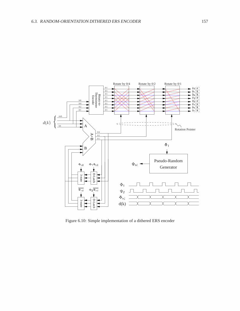
6.3. RANDOM-ORIENTATION DITHERED ERS ENCODER 157
D-L
atchD
-Latch
����������
����������
A
BA
+B
Binary-to-
Therm
ometer
Encoder
3-state3-state
b0(k)b1(k)b2(k)b3(k)b4(k)b5(k)b6(k)b7(k)
Rotate by 0/4 Rotate by 0/2 Rotate by 0/1
d(k) )Rotation Pointer
msb
lsb
0/1
0/2
0/4
0/8
0/1
0/1
0/1
0/1
0/1
0/1
0/1
0/1
0/4
0/2
0/1
�rd �2�rd
�rd �2�rdGenerator
Pseudo-Random�rd
�1
d(k)
�rd
�2
�1
Figure 6.10: Simple implementation of a dithered ERS encoder
158 CHAPTER 6. DITHERING OF MISMATCH-SHAPING DACS
frequency as for un-dithered ERS encoders (the average value of d(k) divided by the number N of unit
elements).
6.3.1 A Family of Dithering Techniques
The following will investigate the possibility of dithering ERS encoders without allowing that any unit
element is used twice before all the other elements have been used in between10. Dithering requires
that equilibrium states are encountered, and that the unit elements then can be selected in at least two
different ways.
Figure 6.11 shows a general technique for the implementation of dithered ERS encoders. With respect to
an arbitrary initial condition (for k = 0), the unit elements are used sequentially11 until they all have been
used once. At this point, an equilibrium state is reached. The equilibrium state is likely to occur in the
middle of a sample, i.e., when the encoder must select more unit elements than there are unused elements
left to choose from. Instead of implementing a simple “wrap-around” event and selecting the extra unit
elements from “the other end” (as for ERS encoders), the extra elements are chosen arbitrarily among
the elements that are not already selected for the present sample. For simplicity, the extra elements
are chosen as a sequence of elements, such that the ERS algorithm can be used. The ERS algorithm
is employed (starting with respect to the new origin) until all the elements have been used twice, at
which point the second equilibrium state is reached. Notice that it is acceptable to alter the orientation
of the rotation between the equilibrium states. This process is continued; every time an equilibrium
state is reached, a new origin and the orientation of rotation are chosen (randomly), whereby the desired
dithered mismatch-shaping characteristic is obtained.
10More precisely, the unit elements must be selected such that there exists an origin in time, for which the outlined condition
is fulfilled.11Obviously, the unit elements may be used in any order, the ERS algorithm is chosen only to simplify the implementation.

6.3. RANDOM-ORIENTATION DITHERED ERS ENCODER 159
������
������
������
d(0) = 4
d(1) = 3
d(2) = 5
d(3) = 5
d(4) = 7
9 > > > > > > > > > > > = > > > > > > > > > > > ;Any 3, any direction
9 > > > > > > > > > > > = > > > > > > > > > > > ;Any 6, any direction
d(5) = 4
9 > > > > > > > > > > > = > > > > > > > > > > > ;Any 3, any direction
d(6) = 2
d(7) = 4
d(8) = 5
Figure 6.11: Identification of equilibrium states.

160 CHAPTER 6. DITHERING OF MISMATCH-SHAPING DACS
6.3.2 Random-Rotation-Scheme Dithering
Simple implementations are in general preferable, and the selection scheme shown in Figure 6.11 is
perhaps a little more general than it needs to be. The unit elements used for d(3), d(5), and d(8) are,
for example, not sequences of neighbor elements, and hence two ERS encoders operating simultane-
ously, an array of logic-and gates, etc., will be required for the implementation. Sufficiently effective
dithering can, however, be obtained even if only the orientation of rotation is chosen randomly when an
equilibrium state is reached, and then the selection process can be designed to choose only sequences
of elements. This simplified dithering technique – called random-orientation dithering – is illustrated in
Figure 6.12. The rotation pointer is marked with an “�” and the target pointer, which (when the element
is used) identifies that an equilibrium state has been reached, is marked with a “Æ.”
������
������
d(0) = 4
d(1) = 3
d(2) = 5
d(3) = 5
d(4) = 7
d(5) = 4
d(6) = 2
d(7) = 4
d(8) = 5
Flip rotation: YES
Flip rotation: NO
Flip rotation: YES
Flip rotation: YES
Figure 6.12: Random-rotation dithering of an ERS encoder.

6.4. CONCLUSION 161
Notice that it is quite simple to keep track of the two pointers. While the orientation of rotation is
maintained, the target pointer remains constant whereas the rotation pointer is updated according to the
ERS algorithm. When the orientation of rotation is altered (occurs randomly when an equilibrium state
is reached), the two pointers are simply interchanged. The dithering effect is obtained because the target
pointer will be a random signal.
The encoder can, for example, be implemented using the topology shown in Figure 4.10 when the latch
is replaced by a small digital state machine (the counterclockwise rotation can be mimicked by adding a
signal-dependent offset to “B”).
Simulated Performance. The proposed random-orientation dithered encoder has been simulated us-
ing the same signals and conditions used for the dithered tree-structure encoder and the dual-ERS en-
coder. The results are shown in Figures 6.13, 6.14, and 6.15. The performance is, unfortunately, not
better than the performance of dual-ERS encoders, which in general are simpler to implement. It is
believed that the unexpected poor performance is due to the relatively slow change in the target pointer.
If, for example, the probability of altering the orientation of the rotation is reduced from 0.5 to (say) 0.3,
then the relatively flat region (10 dB per decade) for OSR less than 10 in Figure 6.14a is extended to
much lower frequencies (not shown).
The performance can probably be improved by also choosing a new origin for every new equilibrium
state, but then the hardware complexity will increase considerably (although it may be worthwhile for
small encoders). A simpler way to improve the performance, for example, would be to constrain the
random process such that the rotation’s orientation is altered for at least every second equilibrium state,
but not more than two times in a row (not tested).
6.4 Conclusion
Idle tones are a serious problem for mismatch-shaping DACs, and it is generally necessary to use some
kind of dithering technique to break the patterns/tones. The tree-structure UE-MS encoder can be ef-
ficiently dithered, but the hardware complexity is considerable. The proposed dual-ERS encoders are
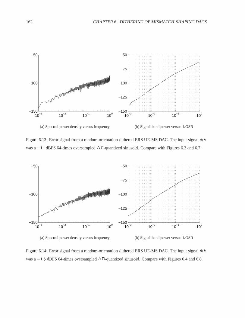
162 CHAPTER 6. DITHERING OF MISMATCH-SHAPING DACS
10−3
10−2
10−1
100
−150
−125
−100
−75
−50
10−3
10−2
10−1
100
−150
−100
−50
(a) Spectral power density versus frequency (b) Signal-band power versus 1/OSR
Figure 6.13: Error signal from a random-orientation dithered ERS UE-MS DAC. The input signal d(k)
was a �12 dBFS 64-times oversampled ��-quantized sinusoid. Compare with Figures 6.3 and 6.7.
10−3
10−2
10−1
100
−150
−125
−100
−75
−50
10−3
10−2
10−1
100
−150
−100
−50
(a) Spectral power density versus frequency (b) Signal-band power versus 1/OSR
Figure 6.14: Error signal from a random-orientation dithered ERS UE-MS DAC. The input signal d(k)
was a �1:5 dBFS 64-times oversampled ��-quantized sinusoid. Compare with Figures 6.4 and 6.8.

6.4. CONCLUSION 163
10−3
10−2
10−1
100
−150
−125
−100
−75
−50
10−3
10−2
10−1
100
−150
−125
−100
−75
−50
10−3
10−2
10−1
100
−150
−125
−100
−75
−50
10−3
10−2
10−1
100
−150
−125
−100
−75
−50
10−3
10−2
10−1
100
−150
−125
−100
−75
−50
10−3
10−2
10−1
100
−150
−125
−100
−75
−50
10−3
10−2
10−1
100
−150
−125
−100
−75
−50
10−3
10−2
10−1
100
−150
−125
−100
−75
−50
Average use 11=16Average use 10=16
Average use 8=16 Average use 9=16
Average use 12=16 Average use 13=16
Average use 15=16Average use 14=16
Figure 6.15: Static performance of a random-orientation dithered ERS UE-MS encoder. The plots show
the signal-band power versus 1/OSR for each constant value of d(k). Compare with Figures 6.5 and 6.9.

164 CHAPTER 6. DITHERING OF MISMATCH-SHAPING DACS
significantly simpler to implement, and the performance is comparable. They have a slight tendency
to produce spread (partially dithered) idle tones, but these “tones” will only appear at high frequencies
and they are seldom a problem. The lowest frequency at which these tones may appear is inversely
proportional to the number of unit elements, and they are hardly noticeable for encoders with only 4 of
8 unit elements. The next chapter will discuss a technique which voids the need for UE-MS DACs of
resolution higher than a few bits.
It is a key point that the shape of the error signal’s spectral power density is dependent on the relative
drive of the encoder. This implies that the OSR cannot be made as low as expected/desired unless the
encoder is designed to have a larger-than-minimum output range. However, for several reasons (cf.
Section 4.4), the average drive will typically be only 50% to 75% of the full range, and hence the effect
is usually not too troublesome12.
12The lower right and left plots in Figures 6.5 6.9, and 6.15 can generally be neglected.

Chapter 7
Scaled-Element Mismatch-Shaping D/A
Converters
Mismatch-shaping DACs are the key element for the implementation of high-resolution wide-bandwidth
A/D and D/A (signal) converters. In Section 4.4.3, it was found that the SER performance of a unit-
element mismatch-shaping (UE-MS) DAC depends mainly on the technology’s matching index (cf.
Equation (4.28)), and not on the inherent resolution of the DAC. The hardware complexity of the digital
UE-MS encoder is, however, only reasonable if the inherent resolution is fairly low, say 5 bits or less,
and hence a �� quantizer/modulator is necessary to encode/interpolate the signal to an oversampled
low-resolution representation.
In Section 4.3.1, it was found that high-performance low-oversampled �� quantizers can be imple-
mented using an only 5-bit representation of d(k), but notice that high-order loop filters and complex
digital multi-rate filters (to decimate the output) are required for the overall implementation. Similarly,
high-performance low-oversampled D/A converter systems can be implemented using an only 5-bit sig-
nal representation; but again, high-order �� modulators and high-performance high-order analog filters
are required for the implementation. In other words, the inherent resolution represents a tradeoff between
the complexity of the encoder and the complexity of the rest of the system. Clearly, the development of
simple high-resolution mismatch-shaping DACs will improve this tradeoff considerably, thereby facili-
165
166 CHAPTER 7. SCALED-ELEMENT MISMATCH-SHAPING D/A CONVERTERS
tating the implementation of much simpler high-performance data converter systems.
7.1 High-Resolution Mismatch-Shaping DACs
Simple high-resolution DACs can be implemented using an array of scaled elements (e.g., the binary-
weighted DAC discussed on page 56); the problem is to make them mismatch-shaping. In fact, it is
impossible to implement a mismatch-shaping DAC using only an encoder and an array of (inaccurately)
binary-scaled elements. To facilitate mismatch-shaping, the array of elements must fulfill the necessary
but not sufficient criteria that each nominal output value can be generated in at least two different ways
(i.e., the DAC must have sub levels [59]). Neither the analog nor the digital portions of the DAC,
however, need be very complex The following discussion will include an example of a mismatch-shaping
DAC based on only two arrays of binary-scaled elements.
7.1.1 General Aspect of the Design of Mismatch-Shaping Encoders
The main issue in the design of scaled-element mismatch-shaping (SE-MS) DACs is, of course, the
design of the digital encoder, which preferably should be made as simple as possible. A good starting
point to solve this problem was provided in Section 4.4.1, where Equation (4.11) expresses the error
signal m(k) produced by a generic DAC of the considered topology (cf. Figure 4.8). The error signal was
expressed as the sum of the gain mismatch errors�PP�1
i=0 [bi(k)[Ki �Kd]]�
and the local nonlinearity
errors�PP�1
i=0 INLi[bi(k)]�
, which were defined with respect to the linear characteristics of the (sub)
DACs
m(k) =
P�1Xi=0
[bi(k)[Ki �Kd]] +
P�1Xi=0
INLi[bi(k)] (7.1)
To make the composite DAC mismatch-shaping, it must be assured that m(k) has only negligible power
in the system’s signal band. The errors can be considered individually.
Controlling the Local Nonlinearity Errors. The local nonlinearity errors can be suppressed in the
signal band if the individual sub DACs are designed as either single-bit or mismatch-shaping DACs.

7.1. HIGH-RESOLUTION MISMATCH-SHAPING DACS 167
In the general case1, most of the P sub DACs will be implemented as (low-resolution) UE-MS DACs.
Notice, however, that the UE-MS DACs need not mutually employ unit elements of the same size; hence,
the number of possible output levels can be vastly higher than the total number of elements. The simplest
implementation will use a binary-weighted array of UE-MS DACs, each comprising only two elements.
Controlling the Gain Mismatch Errors. The nature of the system is that the parameters [Ki �Kd]
are small2, but unknown constants. To obtain the mismatch-shaping property (of the composite DAC),
each of the signals bi(k) must be of the form
bi(k) = Lifd(k)g + h�1(k) � ni(k) (7.2)
where Li are linear operators, h�1(k) is the impulse response of a filter3 that suppresses the signal band
(cf. Section 4.4.4), and ni(k) are (preferably non-tonal) bounded signals. Provided that (7.2) is fulfilled
for all bi(k), the gain mismatch error mgain(k) can be written in the form
mgain(k) =
"P�1Xi=0
[Ki �Kd]�Lifd(k)g + h�1(k) � ni(k)
�#
=
"P�1Xi=0
[Ki �Kd]Lifd(k)g#+ h�1(k) �
"P�1Xi=0
[Ki �Kd]ni(k)
#
= LDACfd(k)g + h�1(k) � nDAC(k) (7.3)
1New types of (e.g., serial) mismatch-shaping DACs are currently being developed; they can often substitute for the more
typical UE-MS DACs.2The sub DACs are designed to have the same nominal gain, and [Ki �Kd] expresses the ith DAC’s gain’s deviation from
the composite DAC’s gain Kd. Kd may be either the average value of the sub DACs’ gains (as for UE-MS DACs), or it may be
the average gain of a subset of the sub DACs (explained in the main text). The constants, [Ki �Kd], are stochastic variables
with zero as the expected value. The standard deviations �i will in general be �i = �processq
jjbi(k)jjjjd(k)jj
, where jj � jj is an
appropriate norm (say, the peak-to-peak value), and �process is the technology’s matching index (with respect to the assigned
chip area).3It need not be the same type/order of filter for all bi(k), but Equation (7.3) becomes confusing if this extra flexibility is
included. The main text will provide several examples of systems where h�1(k) is not the same for all bi(k).
168 CHAPTER 7. SCALED-ELEMENT MISMATCH-SHAPING D/A CONVERTERS
where LDACfd(k)g is an implementation-specific linear operator, which usually will be zero if the
DAC’s gain Kd is defined with respect to the actual implementation, and not as an absolute value4.
Notice that LDAC will be small because the coefficients [Ki�Kd] are small. Hence, mgain(k) will have
the properties required for mismatch-shaping DACs.
7.1.2 Mismatch-shaping Unit-Element DACs – Revisited
To shed some light on the implications of Equations (7.2) and (7.3), consider once again a mismatch-
shaping unit-element DAC with P elements. The UE-MS encoder produces P signals bi(k) with the
same average value, hence Lifd(k)g = d(k)=P for all i. Unless d(k) = 0 or d(k) = P , a truncation
will occur (because bi(k) 2 f0; 1g), which is performed such that bi(k) � Lifd(k)g has the desired
property that bi(k)� d(k)=P = h�1(k) � ni(k).
It may be observed that this point of view leads directly to the parallel UE-MS encoder that was pro-
posed independently by Richard Schreier [12] and Akira Yasuda [53] (shown in a slightly modified
form5 in Figure 7.1). The parallel UE-MS encoder is based on P individual �� modulators (similar
to tree-structure UE-MS encoders), and the correct number of unit elements are selected by varying the
truncators’ threshold value6. Unfortunately, this is, computationally, a complex operation which involves
use of the “sort” function.
7.1.3 Complicated Scaled-Element Mismatch-Shaping Encoders
A scaled-element mismatch-shaping encoder can, in principle, be implemented in a topology similar to
that shown in Figure 7.1, where the individual bi(k) signals control elements of non-uniform values,
4More precisely, the DAC’s signal transfer function is Kd + LDAC; hence, LDAC = 0 if the DAC is free of dynamics
and Kd is defined with respect to the actual implementation. That this is not the only option is exemplified by �� DACs
implemented in the topology shown in Figure 3.24, which will have a signal transfer function close to, but not exactly, Kd. In
that case, LDAC will be a high-pass filter function with only very little gain in the signal band.5For simplicity and graphical purposes, the variable-threshold truncator is not suitable for actual implementations (cf. the
original publication [12]).6Professor Gabor Temes introduced the threshold-control element/idea during a private meeting.

7.1. HIGH-RESOLUTION MISMATCH-SHAPING DACS 169
H(f)
H(f)
H(f)b0(k)
b1(k)
bP�1(k)
Threshold Control
d(k)
P
nP�1(k)
n1(k)
n0(k)
Figure 7.1: Parallel UE-MS encoder.
and where each �� modulator is fed a fraction of d(k) which corresponds to the nominal value of
the respective element. The threshold-control mechanism, however, must be replaced by a vastly more
complex selection mechanism, which assures that the output of the loop filters remains bounded, and
that the sum of the selected elements’ nominal values equals d(k). Overall, the scheme becomes quite
complicated. The interested reader is encouraged to study [59].
7.1.4 Simple Scaled-Element Mismatch-Shaping Encoders
Simple encoders are generally characterized by decentralized calculations which can be performed in
parallel. A useful technique is, for example, to gather elements of the same nominal value in groups, and
let separate UE-MS encoders maintain the mismatch-shaping operation among each group of elements.
The UE-MS encoders can be construed either as part of the sub DACs, which is the approach taken
in the following discussion, or as part of the overall encoder, in which case there are as many sub
DACs as elements. Notice that, either way, this concept complies with the requirement to control local

170 CHAPTER 7. SCALED-ELEMENT MISMATCH-SHAPING D/A CONVERTERS
nonlinearity errors (cf. page 166).
Introducing the Master DAC. Another important technique, which can be used to simplify the en-
coder, is to allow only one of the linear operators Li to be nonzero. In other words, when using this
technique, one of the signals (say b0(k)) is defined as the master signal, which is the only signal that is
correlated7 to the input signal d(k); consequently, the composite DAC’s gain is defined by the master
DAC’s gain, i.e., Kd = K0.
Notice that this technique complies with the fundamental operation of a �� modulator, where the low-
resolution output signal is the master signal. The new element (cf. Figure 7.2) is that the truncation signal
�(k) is not discarded, but separated into one or more compensation signals bi(k); i 6= 0, which are D/A
converted individually and added to the D/A converted master signal. This way, the input signal d(k) is
not truncated and only partially represented by an oversampled lower-resolution signal, but instead re-
encoded and fully represented by the set of spectrally-coded signals bi(k), which are better suitable for
direct D/A conversion with an array of inaccurately matched elements. In other words, the analog output
signal f(k) will not include a large truncation error signal (often called “the shaped quantization noise”),
but will include only the mismatch error signal m(k), which typically is quite small (cf. Equation (4.28)).
The master signal b0(k) automatically fulfills the requirement (7.2), because
b0(k) = d(k) � e(k)
= d(k) � h�1(k) � n0(k) (7.4)
Hence, the only requirements that need be fulfilled to obtain the mismatch-shaping property are that the
compensation signals be of the form
�(k) =
P�1Xi=1
bi(k) (7.5)
bi(k) = h�1(k) � ni(k); i 6= 0 (7.6)
7In the signal band, cf. Equation (7.2).

7.2. A DUAL-TYPE-ELEMENT MISMATCH-SHAPING DAC 171
and that the set of spectrally-coded signals bi(k) be D/A converted using single-bit and/or mismatch-
shaping DACs. Digital systems that fulfill Equations (7.4), (7.5), and (7.6) will hereinafter be called
spectral encoders.
The simplest way to fulfill (7.6) is to omit the separator and let b1(k) = �(k). This technique will be
investigated in the next section, and a discussion of some more advanced separation techniques will
follow.
H(f)d(k) �(k)
Compensation Signals
b1(k)
b2(k)
bP�1(k)
9>>>=>>>;
Master Signal
b0(k)n0(k)
Separator
Figure 7.2: Spectral encoder that separates d(k) into a master signal and one or more compensation
signals with only little signal-band power.
7.2 A Dual-Type-Element Mismatch-Shaping DAC
Figure 7.3 shows a mismatch-shaping DAC controlling elements A0 and A1 of two different nominal
nominal values (with a ratio of 8). The digital input signal d(k) is separated into b0(k) and b1(k) by
the spectral encoder, which is implemented as shown in Figure 7.2, where b1(k) = �(k). For graphic
simplicity, the subtraction block is shown outside the �� modulator, although it will naturally be im-
plemented as a part of the �� modulator.
Resolution of the Spectrally-Encoded Signals. The resolution of the three signals d(k), b0(k), and
b1(k) is an important aspect to consider. This is important because it determines how many elements

172 CHAPTER 7. SCALED-ELEMENT MISMATCH-SHAPING D/A CONVERTERS
Delta-SigmaModulator
A0
A1
b0(k)
b1(k) c1(k)
c0(k)f(k)
4=5
4
4-bit@8
4/5-bit@1
d(k)7
Spectral Encoder
Figure 7.3: Simple dual-type-element mismatch-shaping DAC.
(in A0 and A1) are required for the conversion of d(k) with a given resolution. Preferably, for a simple
encoder, the full-scale range of b1(k) should be small relative to the full-scale range of d(k).
As always for �� modulators, the master signal b0(k) must span at least the same range of values as
the input signal d(k), and usually the range must be a little wider to allow some fluctuation in n0(k) (cf.
Section 4.3.1 and Figure 7.2). In the ideal case, b0(k) will for all k attain one of the two values that are
the closest to the value of d(k), in which case the full-scale range of b1(k) will be about twice as wide
as the step size of b0(k), i.e., a 7-bit input signal can e.g. be spectrally encoded into two 4-bit signals
whereby the unit elements in A1 will be 8 times smaller than the unit elements in A0, and the 128 levels
be represented using only 32 elements. The full-scale range of b1(k) will, however, depend highly on
the design of the �� modulator’s loop filter H(f).
7.2.1 Designing the Delta-Sigma Modulator
The full-scale range of �(k) (cf. Figure 7.2) is a main concern in the design of the spectral encoder’s
�� modulator. To avoid unnecessary8 large values of �(k), the feed-forward branch (from d(k) to
the input of the truncation element) should always be included in the topology (for reasons discussed on
page 76). Assuming, therefore, that the �� modulator’s topology is as shown in Figure 7.2, the only free
parameters are the loop filter’s transfer function H(f) and the master signal’s step size and resolution.
8Unless the feed-forward branch is implemented, the full-scale range of �(k) may, for any loop filter, be at least as large as
the full-scale range of d(k), assuming that d(k) is not spectrally constrained.

7.2. A DUAL-TYPE-ELEMENT MISMATCH-SHAPING DAC 173
If the performance is evaluated only with respect to the full-scale range of �(k), it would be optimal to
use a first-order �� modulator
H(f) =z�1
1 + z�1; where z = ej2�f=fs (7.7)
for which the full-scale range of �(k) is only twice the master signal’s step size. A reason why this may
not always be the best design is that first-order �� modulators are extremely tonal, and hence the gain
error
mgain(k) = b1(k)[K1 �K0] (7.8)
will include gain-error idle tones9, because b1(k) = �(k) includes many strong idle tones that are not
perfectly canceled if [K1 �K0] is nonzero (it is usually in the order of �60 dB).
Avoiding Gain-Error Idle Tones. Essentially, gain-error idle tones can be prevented (suppressed) in
one of two ways. Either �(k) can be separated into several compensation signals bi(k); i 6= 0 in a
nonlinear and aperiodic way (which may turn out to be a risky business), or they can be removed at the
source by designing the �� modulator to be idle-tone free10 using dither [1], chaos [44], or any other of
the well-know techniques. The latter approach is usually much preferable, although it may increase the
magnitude of �(k).
For dither11 to be effective, it should have a uniform probability density function in a range which
is as wide as the master signal’s step size. It is often claimed that the use of dither in multi-bit ��
modulators is “harmless” because it is small relative to full-scale output and hence does not noticeably
affect the stability. This is often true, but dither is actually quite harmful in this context, because the
dither’s magnitude will add linearly to the magnitude of �(k). For example, in a fully dithered first-order
�� modulator, the full-scale range of �(k) will be four times the master signal’s step size, and hence the
compensation DAC A1 is required to have twice an many unit elements as in the un-dithered system.
9In this case they do not originate from the UE-MS DACs, but directly from the spectral encoder.10This is usually not too difficult when the master signal is multi-bit.11Noise added to n0(k), see [1] for details.
174 CHAPTER 7. SCALED-ELEMENT MISMATCH-SHAPING D/A CONVERTERS
Another technique to suppress idle tones is to use a higher-order (i.e., second-order or higher) loop
filter and possibly make it slightly chaotic. It is well understood that idle tones cannot be fully avoided
in this way [1], but considering that the tones will be further suppressed by the gain-matching factor
[K1 �K0], cf. Equation (7.8), they need only be suppressed to (say) �80 dBFS which is quite possible.
The high-order loop filter should not be designed with a high NTFmax value (cf. Section 4.3.1), because
that will vastly increase the magnitude of �(k). The loop filter can, however, easily be of high order
without increasing the magnitude of �(k) noticeably. For example, Figure 4.6 shows that a 6th order
�� modulator with NTFmax = 2 will have a full-scale range of �(k), which is only slightly larger than
twice the master signal’s step size. Notice that the compensation DAC need not employ a power-of-two
number of unit elements; A1 can very well include (say) 22 unit elements. The use of high-order ��
modulators also has the advantage that �(k) will be a high-order shaped signal, hence even a substantial
gain error [K1 �K0] is acceptable with respect to the signal-band performance. In other words, local
matching (i.e., within A0 and A1) is more important than global matching (i.e., K0 relative to K1),
which is an important observation to make use of when the circuit is to be laid out (cf. page 120).
7.2.2 Parallel Work Published
Independent of this work, Robert Adams from Analog Devices Inc. has invented and published [35]
a mismatch-shaping DAC identical to that shown in Figure 7.3. The published system was a high-
resolution DAC where the 20-bit input signal was first interpolated to a 6-bit representation using a
traditional second-order (Candy-structure) �� modulator. This 6-bit signal was D/A converted using a
scaled-element mismatch-shaping DAC of the type shown in Figure 7.3, where the spectral encoder was
of first order. The resolution of the master DAC was 3 bits and the resolution of the compensation DAC
was 4 bits.
Measured Performance. The system worked very well (113 dB performance was reported), although
the used low-order spectral encoder very well could have caused problems (discussed above). During the
question period after the presentation, the speaker’s attention was drawn to the tones that were measured
at the �110 dBFS level. They were claimed to be idle tones from the interpolating �� modulator, and
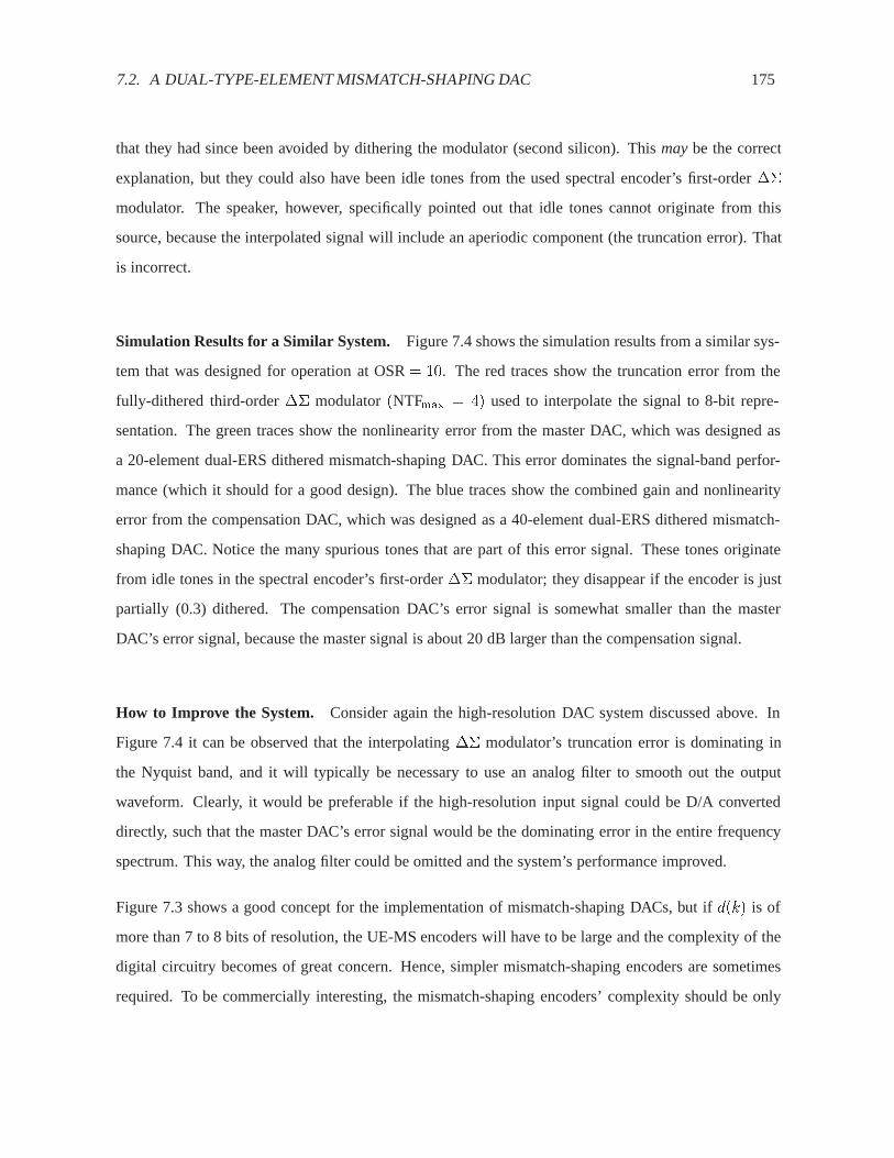
7.2. A DUAL-TYPE-ELEMENT MISMATCH-SHAPING DAC 175
that they had since been avoided by dithering the modulator (second silicon). This may be the correct
explanation, but they could also have been idle tones from the used spectral encoder’s first-order ��
modulator. The speaker, however, specifically pointed out that idle tones cannot originate from this
source, because the interpolated signal will include an aperiodic component (the truncation error). That
is incorrect.
Simulation Results for a Similar System. Figure 7.4 shows the simulation results from a similar sys-
tem that was designed for operation at OSR = 10. The red traces show the truncation error from the
fully-dithered third-order �� modulator (NTFmax = 4) used to interpolate the signal to 8-bit repre-
sentation. The green traces show the nonlinearity error from the master DAC, which was designed as
a 20-element dual-ERS dithered mismatch-shaping DAC. This error dominates the signal-band perfor-
mance (which it should for a good design). The blue traces show the combined gain and nonlinearity
error from the compensation DAC, which was designed as a 40-element dual-ERS dithered mismatch-
shaping DAC. Notice the many spurious tones that are part of this error signal. These tones originate
from idle tones in the spectral encoder’s first-order �� modulator; they disappear if the encoder is just
partially (0.3) dithered. The compensation DAC’s error signal is somewhat smaller than the master
DAC’s error signal, because the master signal is about 20 dB larger than the compensation signal.
How to Improve the System. Consider again the high-resolution DAC system discussed above. In
Figure 7.4 it can be observed that the interpolating �� modulator’s truncation error is dominating in
the Nyquist band, and it will typically be necessary to use an analog filter to smooth out the output
waveform. Clearly, it would be preferable if the high-resolution input signal could be D/A converted
directly, such that the master DAC’s error signal would be the dominating error in the entire frequency
spectrum. This way, the analog filter could be omitted and the system’s performance improved.
Figure 7.3 shows a good concept for the implementation of mismatch-shaping DACs, but if d(k) is of
more than 7 to 8 bits of resolution, the UE-MS encoders will have to be large and the complexity of the
digital circuitry becomes of great concern. Hence, simpler mismatch-shaping encoders are sometimes
required. To be commercially interesting, the mismatch-shaping encoders’ complexity should be only
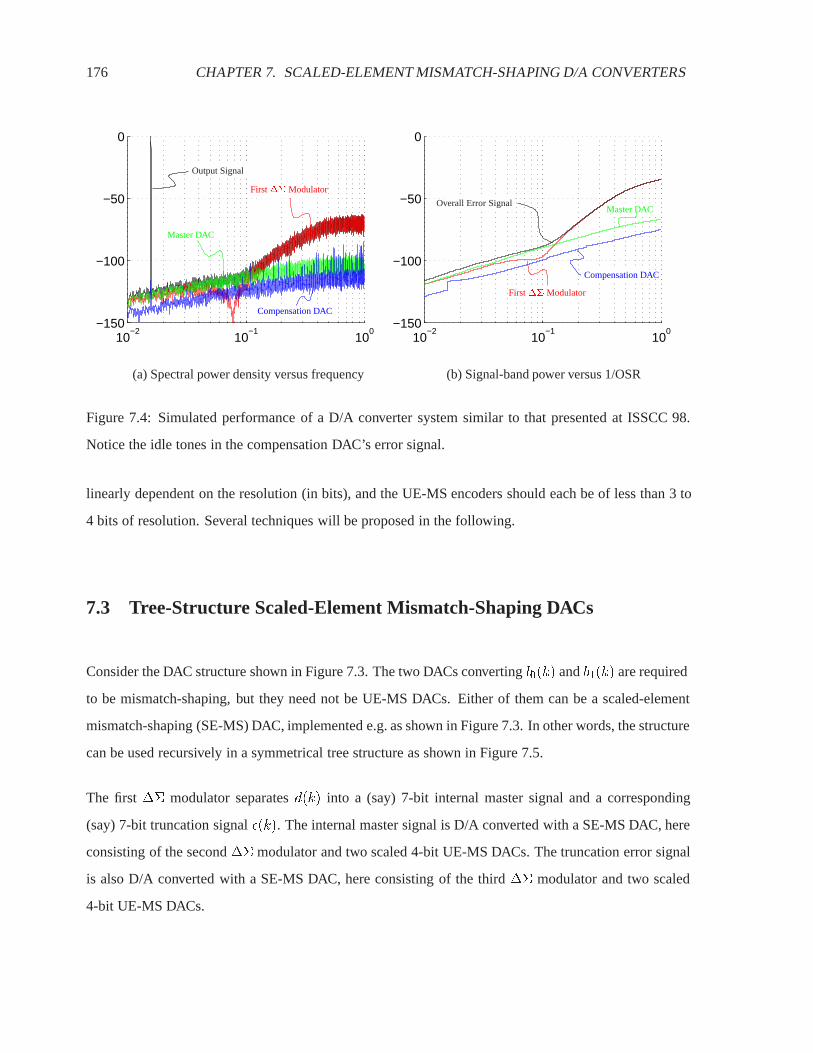
176 CHAPTER 7. SCALED-ELEMENT MISMATCH-SHAPING D/A CONVERTERS
10−2
10−1
100
−150
−100
−50
0
10−2
10−1
100
−150
−100
−50
0
(a) Spectral power density versus frequency (b) Signal-band power versus 1/OSR
Overall Error Signal
Compensation DAC
Master DAC
Output Signal
Compensation DAC
First �� Modulator
First �� Modulator
Master DAC
Figure 7.4: Simulated performance of a D/A converter system similar to that presented at ISSCC 98.
Notice the idle tones in the compensation DAC’s error signal.
linearly dependent on the resolution (in bits), and the UE-MS encoders should each be of less than 3 to
4 bits of resolution. Several techniques will be proposed in the following.
7.3 Tree-Structure Scaled-Element Mismatch-Shaping DACs
Consider the DAC structure shown in Figure 7.3. The two DACs converting b0(k) and b1(k) are required
to be mismatch-shaping, but they need not be UE-MS DACs. Either of them can be a scaled-element
mismatch-shaping (SE-MS) DAC, implemented e.g. as shown in Figure 7.3. In other words, the structure
can be used recursively in a symmetrical tree structure as shown in Figure 7.5.
The first �� modulator separates d(k) into a (say) 7-bit internal master signal and a corresponding
(say) 7-bit truncation signal �(k). The internal master signal is D/A converted with a SE-MS DAC, here
consisting of the second �� modulator and two scaled 4-bit UE-MS DACs. The truncation error signal
is also D/A converted with a SE-MS DAC, here consisting of the third �� modulator and two scaled
4-bit UE-MS DACs.
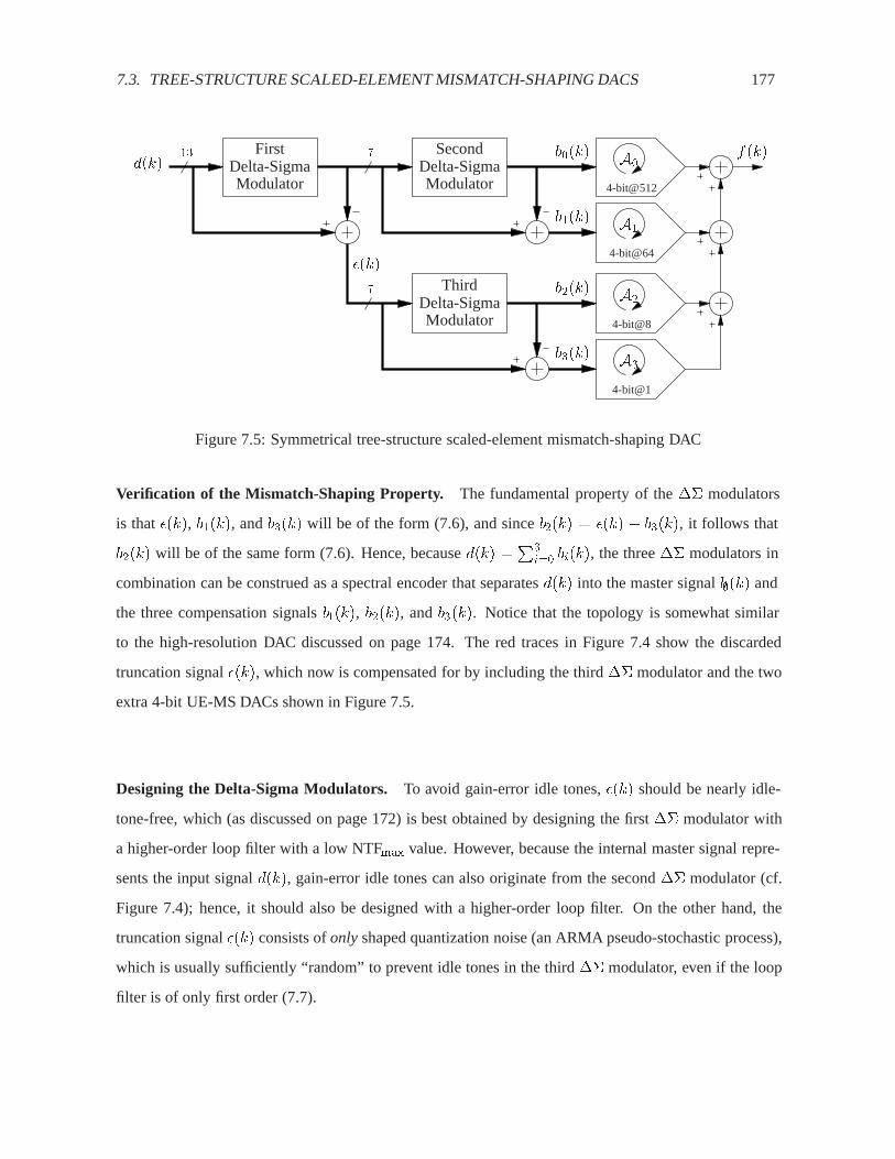
7.3. TREE-STRUCTURE SCALED-ELEMENT MISMATCH-SHAPING DACS 177
A0
A1
A2
A3
SecondDelta-SigmaModulator
FirstDelta-SigmaModulator
ThirdDelta-SigmaModulator
4-bit@512
4-bit@64
4-bit@8
4-bit@1
7
7
f(k)13d(k)
b0(k)
b1(k)
b2(k)
b3(k)
�(k)
Figure 7.5: Symmetrical tree-structure scaled-element mismatch-shaping DAC
Verification of the Mismatch-Shaping Property. The fundamental property of the �� modulators
is that �(k), b1(k), and b3(k) will be of the form (7.6), and since b2(k) = �(k) � b3(k), it follows that
b2(k) will be of the same form (7.6). Hence, because d(k) =P3
i=0 bi(k), the three �� modulators in
combination can be construed as a spectral encoder that separates d(k) into the master signal b0(k) and
the three compensation signals b1(k), b2(k), and b3(k). Notice that the topology is somewhat similar
to the high-resolution DAC discussed on page 174. The red traces in Figure 7.4 show the discarded
truncation signal �(k), which now is compensated for by including the third �� modulator and the two
extra 4-bit UE-MS DACs shown in Figure 7.5.
Designing the Delta-Sigma Modulators. To avoid gain-error idle tones, �(k) should be nearly idle-
tone-free, which (as discussed on page 172) is best obtained by designing the first �� modulator with
a higher-order loop filter with a low NTFmax value. However, because the internal master signal repre-
sents the input signal d(k), gain-error idle tones can also originate from the second �� modulator (cf.
Figure 7.4); hence, it should also be designed with a higher-order loop filter. On the other hand, the
truncation signal �(k) consists of only shaped quantization noise (an ARMA pseudo-stochastic process),
which is usually sufficiently “random” to prevent idle tones in the third �� modulator, even if the loop
filter is of only first order (7.7).
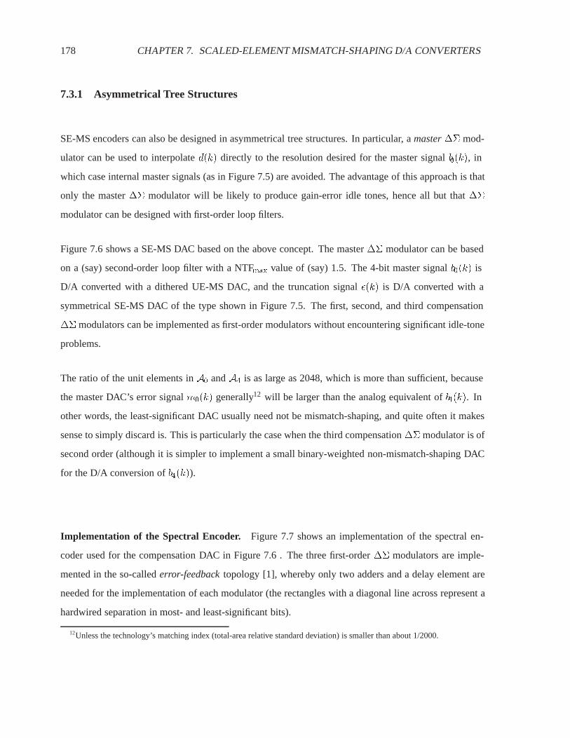
178 CHAPTER 7. SCALED-ELEMENT MISMATCH-SHAPING D/A CONVERTERS
7.3.1 Asymmetrical Tree Structures
SE-MS encoders can also be designed in asymmetrical tree structures. In particular, a master �� mod-
ulator can be used to interpolate d(k) directly to the resolution desired for the master signal b0(k), in
which case internal master signals (as in Figure 7.5) are avoided. The advantage of this approach is that
only the master �� modulator will be likely to produce gain-error idle tones, hence all but that ��
modulator can be designed with first-order loop filters.
Figure 7.6 shows a SE-MS DAC based on the above concept. The master �� modulator can be based
on a (say) second-order loop filter with a NTFmax value of (say) 1.5. The 4-bit master signal b0(k) is
D/A converted with a dithered UE-MS DAC, and the truncation signal �(k) is D/A converted with a
symmetrical SE-MS DAC of the type shown in Figure 7.5. The first, second, and third compensation
�� modulators can be implemented as first-order modulators without encountering significant idle-tone
problems.
The ratio of the unit elements in A0 and A4 is as large as 2048, which is more than sufficient, because
the master DAC’s error signal m0(k) generally12 will be larger than the analog equivalent of b4(k). In
other words, the least-significant DAC usually need not be mismatch-shaping, and quite often it makes
sense to simply discard is. This is particularly the case when the third compensation �� modulator is of
second order (although it is simpler to implement a small binary-weighted non-mismatch-shaping DAC
for the D/A conversion of b4(k)).
Implementation of the Spectral Encoder. Figure 7.7 shows an implementation of the spectral en-
coder used for the compensation DAC in Figure 7.6 . The three first-order �� modulators are imple-
mented in the so-called error-feedback topology [1], whereby only two adders and a delay element are
needed for the implementation of each modulator (the rectangles with a diagonal line across represent a
hardwired separation in most- and least-significant bits).
12Unless the technology’s matching index (total-area relative standard deviation) is smaller than about 1/2000.
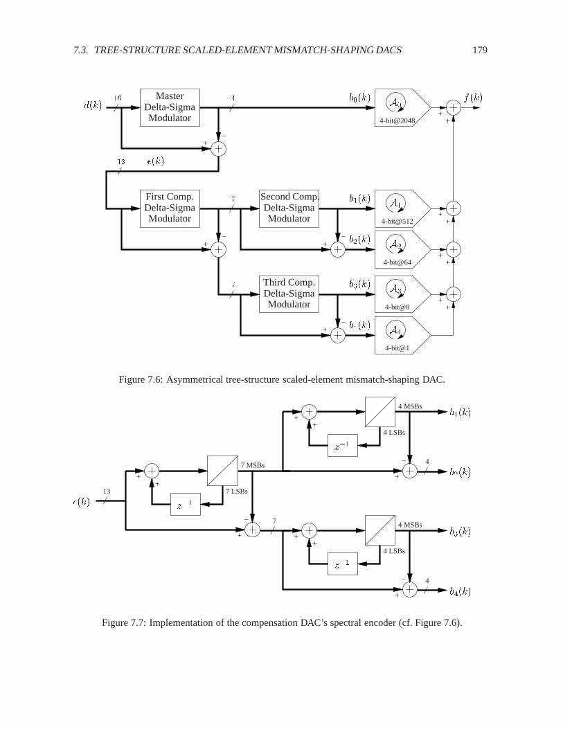
7.3. TREE-STRUCTURE SCALED-ELEMENT MISMATCH-SHAPING DACS 179
A0
4-bit@2048
4 f(k)16d(k)
b0(k)
4-bit@512
4-bit@64
4-bit@8
4-bit@1
7
7
b1(k)
b2(k)
b3(k)
b4(k)
13
A2
A3
A4
A1First Comp.Delta-SigmaModulator
Delta-SigmaModulator
Third Comp.Delta-SigmaModulator
MasterDelta-SigmaModulator
�(k)
Second Comp.
Figure 7.6: Asymmetrical tree-structure scaled-element mismatch-shaping DAC.
13 7 LSBs
7 MSBs
z�1
4 LSBs
4 MSBs
z�1
4 LSBs
4 MSBs
z�1
�(k)
4
4
7
b1(k)
b2(k)
b3(k)
b4(k)
Figure 7.7: Implementation of the compensation DAC’s spectral encoder (cf. Figure 7.6).
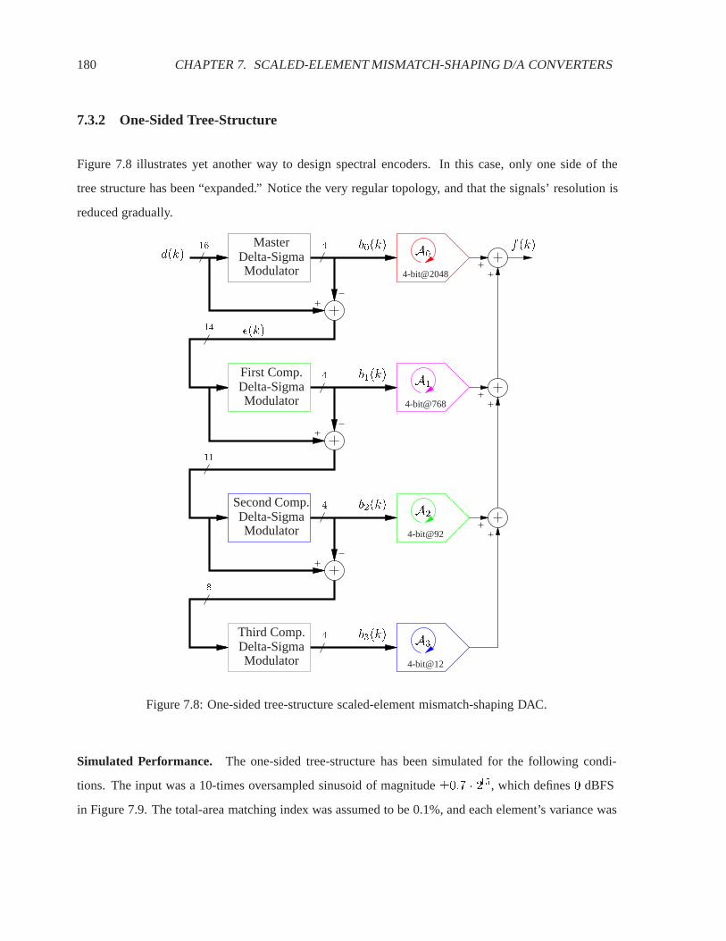
180 CHAPTER 7. SCALED-ELEMENT MISMATCH-SHAPING D/A CONVERTERS
7.3.2 One-Sided Tree-Structure
Figure 7.8 illustrates yet another way to design spectral encoders. In this case, only one side of the
tree structure has been “expanded.” Notice the very regular topology, and that the signals’ resolution is
reduced gradually.
4
4
4
4
A016
d(k)
14
MasterDelta-SigmaModulator
�(k)
First Comp.Delta-SigmaModulator
f(k)
4-bit@2048
Third Comp.Delta-SigmaModulator
4-bit@92
4-bit@768
Second Comp.Delta-SigmaModulator
A2
A1
4-bit@12
A3b3(k)
b2(k)
b1(k)
b0(k)
11
8
Figure 7.8: One-sided tree-structure scaled-element mismatch-shaping DAC.
Simulated Performance. The one-sided tree-structure has been simulated for the following condi-
tions. The input was a 10-times oversampled sinusoid of magnitude �0:7 � 215, which defines 0 dBFS
in Figure 7.9. The total-area matching index was assumed to be 0.1%, and each element’s variance was

7.3. TREE-STRUCTURE SCALED-ELEMENT MISMATCH-SHAPING DACS 181
assumed to be inversely proportional to the element’s value relative to the sum of all the elements. The
master �� modulator was of second order (NTFmax = 1:5) and the three other �� modulators were of
first order (NTFmax = 2). �(k) was represented by 14 bits to avoid unintentional truncation, but since
it would not span the whole range, the elements in A1 were chosen 6 and not 4 times smaller than the
elements in A013.
The black traces in Figure 7.9 show the simulated overall performance, whereas the colored traces show
the combined gain and nonlinearity errors from the individual DACs (the colors are chosen according
to the color code used in Figure 7.8). The master DAC’s nonlinearity error limits the performance in
the entire frequency spectrum, and 100 dB performance was obtained at about 30 times oversampling.
Notice that the truncation error caused by the third compensation �� modulator is not dominating (cyan
trace m4(k) = b4(k)K0, where b4(k) = d(k)�P3i=0 bi(k)).
10−2
10−1
100
−150
−100
−50
0
10−2
10−1
100
−150
−100
−50
0
(a) Spectral power density versus frequency (b) Signal-band power versus 1/OSR
Output Signal
Overall Error Signal m0(k)
m1(k)
m2(k) m3(k)
m4(k)
Figure 7.9: Performance of the one-sided tree-structure SE-MS DAC shown in Figure 7.8.
13The simplest way to implement this technique is to multiply �(k) by 3/2 (or 5/4 for a more aggressive design) and set the
gain of the compensation DAC to 2/3 (or 4/5) of the master DAC’s gain K0, simply by scaling the elements accordingly.

182 CHAPTER 7. SCALED-ELEMENT MISMATCH-SHAPING D/A CONVERTERS
7.4 Filtering Scaled-Element Mismatch-Shaping DACs
The following refers to Figure 7.2. The design of the master DAC is a separate issue, but generally it
is preferable to implement the compensation DAC as simple as possible, which usually implies that the
compensation signals should be of very low resolution. A tree-structure spectral encoder can be used
to separate the truncation signal �(k) to almost any low resolution (two bits), but doing so is a tradeoff
between the spectral encoder’s complexity (cf. Figure 7.7) and the UE-MS encoders’ complexity (cf.
Figures 4.10 and 6.10). This section will propose an even simpler filtering spectral encoder, where the
separation of �(k) into 3-level compensation signals is very simple to implement.
The Filtering Principle. In section 7.1.4 it was discussed that the compensation signals should be of
the form (cf. Equation (7.6))
bi(k) = h�1 � ni(k); i 6= 0 (7.9)
and in Figure 7.2 it can be observed that �(k) = h�1(k) � n0(k), where h�1(k) is the impulse response
of 1=H(f). Because filtering is a linear operation, it follows that
n0(k) =
P�1Xi=1
ni(k) and �(k) = h�1(k) � n0(k) (7.10)
+
�(k) =P�1Xi=1
bi(k) and bi(k) = h�1(k) � ni(k); i 6= 0 (7.11)
which means that if n0(k) is separated in any way into a set of signals ni(k); i 6= 0, and these signals
are filtered individually by 1=H(f), then the outcome will be a set of compensation signals bi(k) with
the desired property14 (7.9). To simplify the circuit, the compensation signals should preferably be of
low resolution. This can be obtained, for example, if ni(k); i 6= 0, are single-bit signals and h�1(k) is
a first-order difference filter. The following discussion will provide several examples of the use of this
very powerful concept.
14For the system to be implementable, h�1(k) must be a causal filter, which requires that H(f) be non-delaying. The
feedback loop, however, must include one sample of delay for the �� modulator to be stable. This delay is best inserted after
the loop filter H(f) and before n0(k) is added to d(k). See the main text for several examples.
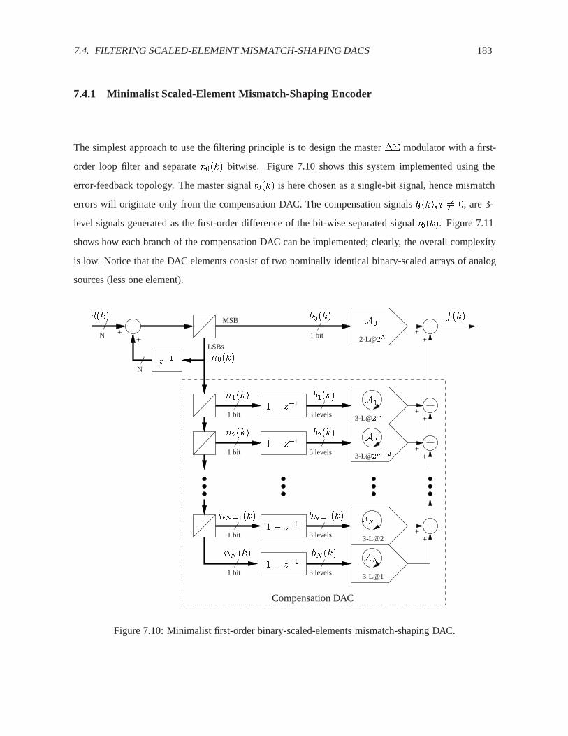
7.4. FILTERING SCALED-ELEMENT MISMATCH-SHAPING DACS 183
7.4.1 Minimalist Scaled-Element Mismatch-Shaping Encoder
The simplest approach to use the filtering principle is to design the master �� modulator with a first-
order loop filter and separate n0(k) bitwise. Figure 7.10 shows this system implemented using the
error-feedback topology. The master signal b0(k) is here chosen as a single-bit signal, hence mismatch
errors will originate only from the compensation DAC. The compensation signals bi(k); i 6= 0, are 3-
level signals generated as the first-order difference of the bit-wise separated signal n0(k). Figure 7.11
shows how each branch of the compensation DAC can be implemented; clearly, the overall complexity
is low. Notice that the DAC elements consist of two nominally identical binary-scaled arrays of analog
sources (less one element).
3-L@1
AN
A2
nN�1(k)
n2(k)1� z�1
1 bit
1� z�11 bit
nN (k)1� z�1
1 bit
b2(k)
3 levels
3 levels
bN (k)
3 levels
n1(k)1� z�1
1 bit
b1(k)
3 levels
bN�1(k)
A1
3-L@2
3-L@2N�2
3-L@2N�1
AN�1
LSBs
MSB
z�1
b0(k)
1 bit
f(k)
N
N
d(k)
n0(k)
A0
2-L@2N
Compensation DAC
Figure 7.10: Minimalist first-order binary-scaled-elements mismatch-shaping DAC.

184 CHAPTER 7. SCALED-ELEMENT MISMATCH-SHAPING D/A CONVERTERS
000001010011100101110
110011
110001111100001
abc xyz
c
b
a
x
z
y
000
D
D
clk
clk
111
1 bit@2N�i
1 bit@2N�i
ni(k)
Figure 7.11: State machine implementing first-order differentiation and mismatch shaping.
7.4.2 Practical Filtering Scaled-Element Mismatch-Shaping DACs
The SE-MS DAC shown in Figure 7.10 may be simple, but the topology is not the most suitable for the
implementation of high-performance DACs. The problem is that the first-order master �� modulator is
almost certain to generate idle tones, and gain error will make them leak to the output f(k). As usual,
this problem can be avoided by increasing the order of the loop filter; but to minimize the resolution
of the compensation signals bi(k); i 6= 0, first-order difference filtering of ni(k) is preferable. These
two requirements can be fulfilled simultaneously when the spectral encoder is designed as shown in
Figure 7.12. The basic idea is that the loop filter is realized as a cascade of two stages, where the first
stage has the desired transfer function and the second stage is designed to keep the �� modulator stable.
The loop filter’s NTFmax value should be fairly low (say 1:5) to assure that the full-scale range of n0(k)
is reasonably small. The full-scale range of n0(k) is proportional to the step size of the master DAC.
For a first-order loop filter (cf. Figure 7.10) n0(k) will be as large as the master DAC’s step size, but for
higher order loop filter’s it may be up to about 1.5 times larger (for low values of NTFmax). Although
it usually is not necessary, the presented design incorporates a safety factor (to prevent unintentional
truncation) by using elements of the same value in A0 and A1. The design can be improved slightly by
increasing the master DAC’s step size by about one third to 432
N�1. The �� modulator must then be

7.4. FILTERING SCALED-ELEMENT MISMATCH-SHAPING DACS 185
modified accordingly, but that is a simple matter.
11�z�1
A0
3 bit@2N�1
Compensation DAC
3-L@1
AN
A2
nN�1(k)
n2(k)1� z�1
1 bit
1� z�11 bit
nN(k)1� z�1
1 bit
b2(k)
3 levels
3 levels
bN (k)
3 levels
1� z�11 bit
b1(k)
3 levels
bN�1(k)
A1
3-L@2
3-L@2N�2
3-L@2N�1
AN�1
N+2
d(k) 54z�1�z�2
1�z�1
b0(k)
3 bit
f(k)
n0(k)
n1(k)
Figure 7.12: Improved SE-MS DAC that is less subject to gain-error idle tones.
7.4.3 Reducing the Gain-Error Sensitivity
Usually, it is the master DAC’s error signal that limits the performance. This is, however, not the case
when the master DAC is linear, e.g., if b0(k) is a single-bit signal, in which case the compensation DAC’s
error signal will dominate. Because this design approach bears some interest (discussed later), it is worth
while to consider how the compensation DAC’s error signal can be minimized.
The compensation DAC’s error signal is the sum of the internal DACs’ error signals m1(k); m2(k); : : : ;
mN (k). Each of the error signals consist of two parts: the gain error bi(k)[Ki � K0] and the local

186 CHAPTER 7. SCALED-ELEMENT MISMATCH-SHAPING D/A CONVERTERS
mismatch error. The local mismatch errors will almost always be first-order shaped (when first-order
UE-MS encoders are used). The gain errors are, however, likely to be larger15, because they depend on
global matching of electrical parameters, and because the individual DACs often will be implemented
with some physical distance. It is, therefore, preferable if the compensation signals bi(k) are more-than-
first-order shaped, i.e., of the form (7.9), where h�1(k) is a higher-order filter (cf. Figure 4.11).
Clearly, second-order shaped compensation signals bi(k) can be obtained by designing the master ��
modulator’s first filter stage as a second-order integrator (cf. Figure 7.12) and employing second-order
difference filters in the compensation DAC. This is, however, not a good idea. The problem is that the
magnitude of n0(k) will increase (even for the same NTFmax value), and the second-order difference
filters will further increase the magnitude of the compensation signals by a factor of two. This way, the
reduction of the gain error’s signal-band power, due to a higher-order shaping of bi(k), is lost because the
Nyquist-band power of the error signals is increased. This is especially a problem for the local mismatch
errors, which will remain first-order shaped.
Fortunately, there are other and better ways to higher-order shape the compensation signals. In Fig-
ure 7.12, n0(k) is first-order shaped (because it is the input signal to an integrator for which the output
signal is bounded), but the spectral composition is immediately destroyed by splitting the signal bitwise.
Figure 7.13 shows how the spectral encoder can be modified such that n1(k) inherits the first-order-
shaped property of n0(k). The property is inherited, because n1(k) is the difference between n0(k) and
the first-order difference of n�0(k), which are both first-order shaped16.
The Nyquist-band powers of the error signals are largely proportional to the square root of the corre-
sponding DACs’ step size. Hence, if A1 includes (say) 8 elements, it is mainly the gain error of m1(k)
that is of concern. In other words, for simplicity, it would be better if the secondary compensation sig-
nals, b2(k); b3(k); : : : ; bN (k), could be of only 3-level resolution, even if that were to imply that they
would be only first-order shaped. This simplification can be obtained, for example, by differentiating
n�0(k) before it is split bitwise (not shown). An even simpler technique to obtain the same result is shown
15Nyquist-band power.16Except for the differentiation of n0(k), the compensation DAC is identical to the minimalist SE-MS DAC shown in
Figure 7.10).
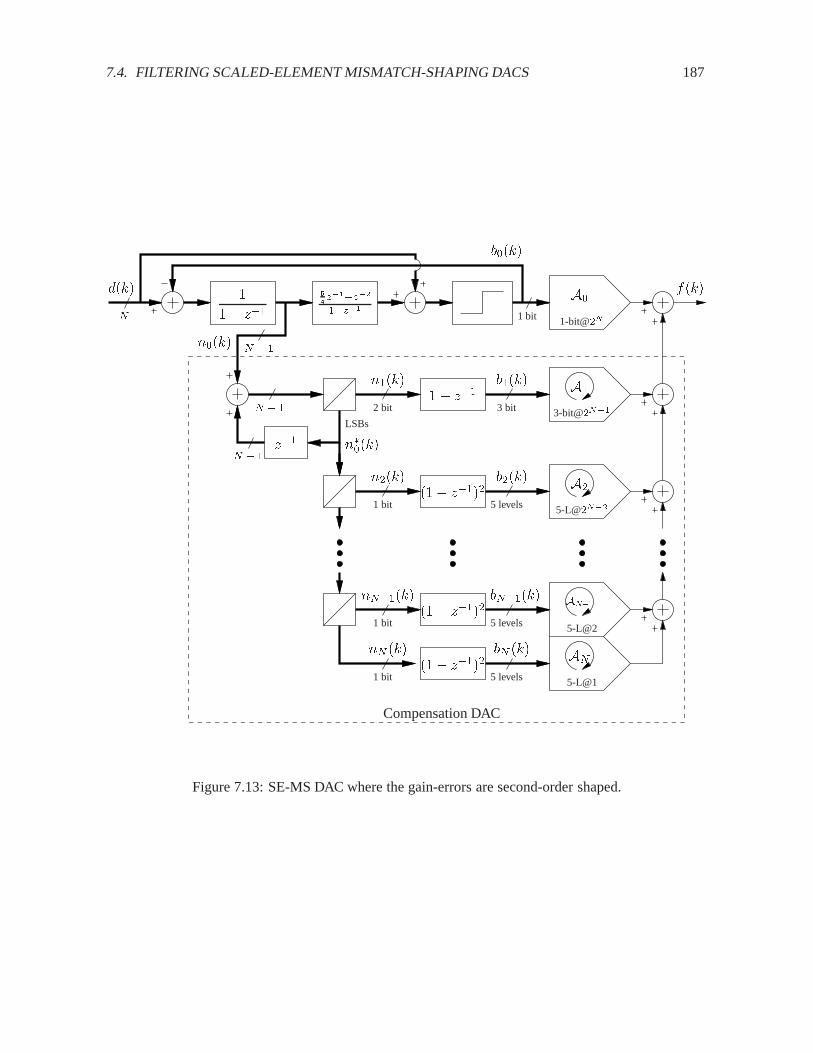
7.4. FILTERING SCALED-ELEMENT MISMATCH-SHAPING DACS 187
1� z�1
A0
1-bit@2NN
d(k)
b0(k)
1 bit
f(k)
5-L@1
AN
A2
nN�1(k)
n2(k)
1 bit
1 bit
nN (k)
1 bit
b2(k)
5 levels
bN (k)
bN�1(k)
5-L@2
5-L@2N�2
AN�1
2 bit
b1(k) A1
3-bit@2N�1
z�1N � 1
LSBs
5
4z�1�z�2
1�z�1
N + 1
Compensation DAC
N + 1
3 bit
(1� z�1)2
(1� z�1)2
(1� z�1)2
5 levels
5 levels
n0(k)
1
1� z�1
n1(k)
n�0(k)
Figure 7.13: SE-MS DAC where the gain-errors are second-order shaped.

188 CHAPTER 7. SCALED-ELEMENT MISMATCH-SHAPING D/A CONVERTERS
in Figure 7.14. In essence, the topology is equivalent to that shown in Figure 7.3, where the compensa-
A0
1-bit@2NN
d(k)
b0(k)
1 bit
f(k)
3-L@1
AN
A2
nN�1(k)
n2(k)1� z�1
1 bit
1� z�11 bit
nN (k)1� z�1
1 bit
b2(k)
3 levels
3 levels
bN (k)
3 levels
bN�1(k)
3-L@2
3-L@2N�2
AN�1
3 bit
b1(k) A1
3-bit@2N�1
z�1N � 1
LSBs
n1(k)
5
4z�1�z�2
1�z�11
1�z�1
�(k)
N + 2
N + 2
Compensation DAC
Figure 7.14: Alternative to Figure 7.13 where the compensation signals are shaped according to their
magnitude.
tion DAC is implemented as the minimalist SE-MS DAC shown in Figure 7.10. The main compensation
signal n1(k) will inherit the spectral composition17 of �(k) because gain errors within the compensation
DAC can be referred to the secondary compensation signals b2(k); b3(k); : : : ; bN (k). In principle, a few
of the least significant compensation signals can be gathered in one signal (of say 4-bit resolution) and
17In this case, it is second-order shaped.
7.5. SECOND-ORDER SCALED-ELEMENT MISMATCH-SHAPING DACS 189
D/A converted with a non-mismatch-shaping DAC. The local mismatch error from this DAC will not be
shaped, but be a very small pseudo-white-noise signal (the gain error remains first-order shaped).
7.5 Second-Order Scaled-Element Mismatch-Shaping DACs
In principle, it is very simple to design second-order SE-MS DACs; just use second-order UE-MS DACs
and assure that the compensation signals are at least second-order shaped (e.g., using any tree-structure
topology with second-order �� modulators, or an appropriate filtering structure, such as that shown
in Figure 7.13). This approach is, however, not too attractive, because second-order UE-MS shaping
encoders are complicated to implement and only truly effective if the OSR is 25 or larger. The purpose
of increasing the order of the mismatch shaping is typically to allow the use of lower OSR, hence the
second-order structures discussed above are only relevant in extreme situations (or if better and simpler
second-order UE-MS encoders are invented). The following will discuss a technique by which effective
second-order mismatch shaping can be obtained without using second-order UE-MS encoders.
7.5.1 The Generalized Filtering Principle
Consider again the SE-MS DAC shown in Figure 7.13. If, for example, the master signal b0(k) is of 1-bit
resolution, the master DAC can be made linear. In that case, it is entirely the compensation DAC that
limits the system’s performance. The compensation DAC’s gain errors can easily be made second- or
even higher-order shaped (cf. Section 7.4.3), but in the absence of good second-order mismatch-shaping
encoders, the compensation DAC’s local nonlinearity errors will be only first-order shaped. If, however,
the compensation DAC’s output is filtered (differentiated) in the analog domain, the local nonlinearity
errors will be shaped also by this filter’s transfer function. This way, efficient second- or higher-order
mismatch-shaping is made feasible; it can be implemented as shown in Figure 7.15.

190 CHAPTER 7. SCALED-ELEMENT MISMATCH-SHAPING D/A CONVERTERS
1� z�1
1� z�1
1� z�1
1� z�1
A0
1-bit@2NN
d(k)
b0(k)
1 bit
f(k)5
4z�1�z�2
1�z�11
1� z�1
3-L@1
A2b2(k)
3 levels
bN�2(k)
3-L@2
3-L@2N�3
b1(k) A1
3-bit@2N�2
z�1N � 1
LSBs
N + 1
1� z�1
1� z�1
1� z�1
n�0(k)
nN�2(k)
n2(k)
1 bit
1 bit
1 bit
3 bit
n0(k)
N + 1
3 levels
3 levels
Compensation DAC
AN�2
nN�1(k) bN�1(k) AN�1
Figure 7.15: Second-order filtering SE-MS DAC employing analog filters.

7.5. SECOND-ORDER SCALED-ELEMENT MISMATCH-SHAPING DACS 191
7.5.2 The Filter-Mismatch Problem
The generalized filtering principle has similarities to the MASH structure [1] and its cousin – the dual-
quantization DACs [60]. Since the performance of these circuits is critically dependent on matching an
analog filter’s transfer function to the (master) �� modulator’s (noise) transfer function, a discussion of
this issue is found to be appropriate.
The MASH structure was discussed18 on page 89, and it was concluded that the �� modulator generally
should not be chosen of an order higher that two, because the impact of mismatch of the analog/digital
filters’ transfer functions on the system’s performance will increase with the filters’ order. The argument
that filter mismatch is a problem19 even for only second-order systems is supported by the many circuit-
level techniques developed to improve the matching [60].
The reason why filter mismatch is much less of a problem when using the generalized filtering principle
is that the performance, even for high-order master �� modulators, does not rely on matching of high-
order filters. Consider Figure 7.15. It can be observed that the relation d(k) = b0(k)+[n0(k)�n0(k�1)]is a consequence only of n0(k) is the accumulation of d(k) � b0(k). In other words, the relation is
completely independent of the second filter stage of the master �� modulator20. Hence, the analog filter
is to match only the master �� modulator’s first filter stage (which typically is of low order), and not the
modulator’s high-order noise transfer function. As opposed to MASH and dual-quantization DACs, the
signal-band performance of generalized filtering DACs will improve when the master �� modulator’s
order is increased21, because n0(k) will have increasingly less signal-band power. Consequently, the
cancellation process need not be relied upon in the signal band. In the extreme case, such as for very
poor filter matching and master �� modulators of high order, the compensation DAC can be construed
as a simpler substitute for the smoothening filter shown in Figure 3.9. However, usually it is possible to
obtain quite good matching of low-order filters, whereby state-of-the-art performance can be obtained
18Only the MASH quantizer structure was discussed, but the filter-matching issue is the same for MASH DACs.19It is only a problem if you aim at high (say more than 85 dB) performance.20The second filter stage affects mainly the magnitude (through NTFmax) and the spectral composition (through the filter’s
order) of n0(k).21Assuming that the master �� modulator’s first filter stage and the analog filter remains the same.
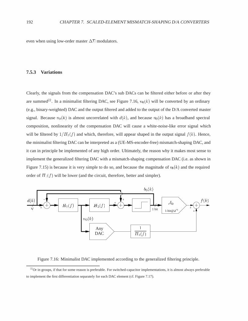
192 CHAPTER 7. SCALED-ELEMENT MISMATCH-SHAPING D/A CONVERTERS
even when using low-order master �� modulators.
7.5.3 Variations
Clearly, the signals from the compensation DAC’s sub DACs can be filtered either before or after they
are summed22. In a minimalist filtering DAC, see Figure 7.16, n0(k) will be converted by an ordinary
(e.g., binary-weighted) DAC and the output filtered and added to the output of the D/A converted master
signal. Because n0(k) is almost uncorrelated with d(k), and because n0(k) has a broadband spectral
composition, nonlinearity of the compensation DAC will cause a white-noise-like error signal which
will be filtered by 1=H1(f) and which, therefore, will appear shaped in the output signal f(k). Hence,
the minimalist filtering DAC can be interpreted as a (UE-MS-encoder-free) mismatch-shaping DAC, and
it can in principle be implemented of any high order. Ultimately, the reason why it makes most sense to
implement the generalized filtering DAC with a mismatch-shaping compensation DAC (i.e. as shown in
Figure 7.15) is because it is very simple to do so, and because the magnitude of n0(k) and the required
order of H1(f) will be lower (and the circuit, therefore, better and simpler).
A0
1-bit@2NN
d(k)
b0(k)
1 bit
f(k)H2(f)H1(f)
n0(k)
AnyDAC
1
H1(f)
Figure 7.16: Minimalist DAC implemented according to the generalized filtering principle.
22Or in groups, if that for some reason is preferable. For switched-capacitor implementations, it is almost always preferable
to implement the first differentiation separately for each DAC element (cf. Figure 7.17).

7.5. SECOND-ORDER SCALED-ELEMENT MISMATCH-SHAPING DACS 193
7.5.4 Switched-Capacitor Implementation
Figure 7.17 shows a switched-capacitor (SC) implementation of the second-order SE-MS DAC shown
in Figure 7.15 (the spectral encoder is not shown).
The analog output signal f(k) is represented as charge pulses dumped to the opamp’s virtual-ground
node, and it is low-pass filtered and converted into a voltage signal vout(k) by the switched-RC feedback
network. The linearity of the D/A conversion does not particularly depend on the ideality of the provided
virtual ground potential, but (of course) the SC circuit must meet the overall performance requirements.
The summation of the individual charge-pulse signals ci(k) will be ideal (charge conservation).
The master DAC will (in clock phases �1 and as a function of b0(k)) provide charge pulses of �VrefC ,
hence the system’s gain is
Kd = K0 =2VrefC
2N=VrefC
2N�1(7.12)
It is important that c0(k) is in linear relation with b0(k), hence the usual precautions for the implemen-
tation of single-bit SC DACs’ should be observed. It is particularly important that the load seen by
the reference voltage is independent of b0(k) (see [1] for a detailed discussion). Also, the Haigh-and-
Singh delayed-clock-phases clocking scheme should (as always for high-performance SC circuits) be
employed to prevent signal-dependent charge injection and clock feedthrough [29].
The primary compensation DAC is implemented by a UE-MS driver and 8 nominally-identical capaci-
tors23 of capacitance C=4. The capacitor terminals that are connected to the virtual-ground node are not
switched, hence the charge-pulse signal c1(k) will be the first-order difference of the weighted voltage
signal provided by the UE-MS driver. Each capacitor is driven by a single-bit logic signal (with the step
size of 2N�2) which is buffered to �Vref (as shown for b0(k) in the master DAC). Hence, each capacitor
will provide charge pulses of either �2VrefC=4, 0, or 2VrefC=4, and the gain of this DAC will be
K1 =2VrefC=4
2N�2=VrefC
2N�1(7.13)
236 capacitors would in principle be enough, because b1(k) does not span the full range. 8-element UE-MS encoders are,
however, particularly simple to implement.

194 CHAPTER 7. SCALED-ELEMENT MISMATCH-SHAPING D/A CONVERTERS
+
C
C=4
b1(k)
+Vref
�Vref
b0(k)
�2�2
�1 �1�2 �2
�1
b0(k) � �1
b0(k) � �1 Master DAC
CompensationPrimary
DAC
3
1
Digital Circuits are Clocked on
All Logic Levels are �Vrefthe Rising Edge of �1
vout(k)
f(k)
c0(k)
c1(k)
C=8
C=16
C=2N
CompensationSecondary
DACs
3 levels
3 levels
3 levels
C=2N�1
cN�1(k)
cN�2(k)
c3(k)
c2(k)3 levelsb2(k)
b3(k)
bN�2(k)
bN�1(k)
Figure 7.17: Switched-capacitor implementation of the analog part of the second-order filtering SE-MS
DAC shown in Figure 7.15.

7.5. SECOND-ORDER SCALED-ELEMENT MISMATCH-SHAPING DACS 195
which conforms with the master DAC’s gain.
The analog-domain differentiation will match the digital-domain integration exceptionally well, because
the ideality of the analog filter relies only on the electrical insulation of each capacitor’s two terminals.
In other words, unless the sampling frequency is extremely low and the capacitors’ leakage current large
(e.g., caused by high-temperature operation or a very bad technology), the analog filter can be assumed
ideal for all practical purposes.
The secondary compensation DACs are implemented similar to the primary compensation DAC.
Simulation Results. The circuit was simulated (with MATLAB) using the assumptions outlined on
page 180. The results are shown in Figure 7.18. The black traces show the overall performance. The
error signal is second-order shaped (the signal-band error power decreases 50 dB per decade of oversam-
pling), and it is observed that 100 dB performance is obtained at 10 times oversampling (the target for
this work). Because the error signal is higher-order shaped, the OSR required for 100 dB performance
will be less dependent on the technology’s matching index.
The master DAC is linear, hence it produces no local nonlinearity error. The master DAC, however,
defines the system’s gain Kd, which should carefully be matched to the (primary) compensation DAC’s
gain to minimize gain errors. The primary compensation DAC’s combined gain and local nonlinearity
error is shown with green traces. This is the dominating error source, which it should be because the
primary compensation signal c1(k) is somewhat larger than the secondary compensation signals. The
combined error signal from the secondary compensation DACs is shown with blue traces (only the 8
most-significant secondary compensation DACs were included). Notice the small gain-error idle tones
that occur at high frequencies. These tones are so small that they usually do not represent a problem, but
it is interesting to observe that they indeed do exist.
In comparison with the previous shown simulation results (Figures 7.4 and 7.9), the error signal’s
Nyquist-band power is approximately 6 dB larger. This is because the primary compensation DAC,
which produces the dominating error signal, can produce a signal which is 6 dB larger than a full-scale
output signal. This is in itself not a major problem (because the error signal is second-order shaped);
196 CHAPTER 7. SCALED-ELEMENT MISMATCH-SHAPING D/A CONVERTERS
but since the magnitude of c1(k) is proportional to the master DAC’s step size, 6 dB improvement (in
the entire frequency spectrum) can be obtained if a linear 3-level master DAC can be realized (discussed
below).
To facilitate comparison, Figure 7.19 shows the equivalent simulation results for the system shown in
Figure 7.13. Here, the first-order-shaped local nonlinearity errors are dominating, hence the perfor-
mance is not as good as in Figure 7.18. The error signal’s Nyquist-band power is equally high, so the
performance is not even as good as for the other proposed first-order shaping systems (compare Fig-
ures 7.9 and 7.19). As discussed above, this first-order system may, however, perform better than the
other proposed first-order systems because the gain errors are second-order shaped. In actual implemen-
tations, gain errors are likely to dominate the local nonlinearity errors (because of physical distance in
the layout), but this parameter was not included in the stochastic model used for the simulations.
Figure 7.20 shows the second-order SE-MS DAC’s time-domain output signal f(k) for a saw-tooth input
signal d(k). Clearly, the error signal is very small, and there is hardly a need for a filter dedicated to
suppress it further (for example, for audio applications, the human ear can maintain this function). It
should, however, by understood that the signal shown is highly oversampled, and that there may be a
need for a filter dedicated to suppress replica spectral images (cf. Section 3.2.1).
Experimental Work. A fully-differential version of the SC DAC shown in Figure 7.17 has been im-
plemented in cooperation with MEAD Microelectronics in Switzerland.
The spectral encoder and the primary compensation DAC’s UE-MS encoder was implemented using an
external FPGA, and the SC circuit was implemented in a 5-Volt 0:8�m CMOS technology. Because
the DAC’s error signal has only little Nyquist-band power, the voltage signal vout(k) was DT/CT con-
verted directly with a zero-order holding circuit (cf. Figure 3.9). A replication-rejection filter was not
implemented.
The target performance was 100 dB SNDR at 10 times oversampling with a sampling frequency in the
range from 400 kHz to 1 Mhz (i.e., a signal bandwidth of 20 kHz to 50 kHz). The targeted low OSR
and high SNR requires that large signal capacitors be used to avoid thermal-noise limitation; the master

7.5. SECOND-ORDER SCALED-ELEMENT MISMATCH-SHAPING DACS 197
10−2
10−1
100
−150
−100
−50
0
10−2
10−1
100
−150
−100
−50
0
(a) Spectral power density versus frequency (b) Signal-band power versus 1/OSR
Output Signal
Overall Error Signal
Primary Comp. DAC
Secondary Comp. DACs
Figure 7.18: Simulated performance of the second-order SE-MS DAC shown in Figures 7.15.
10−2
10−1
100
−150
−100
−50
0
10−2
10−1
100
−150
−100
−50
0
(a) Spectral power density versus frequency (b) Signal-band power versus 1/OSR
Output Signal
Overall Error Signal
Primary Comp. DAC
Secondary Comp. DACs
Figure 7.19: Simulated performance of the first-order SE-MS DAC shown in Figure 7.13.

198 CHAPTER 7. SCALED-ELEMENT MISMATCH-SHAPING D/A CONVERTERS
0 2000 4000 6000 8000 10000−1
0
1
5900 6000 61000
0.05
0.1
Figure 7.20: Time-domain performance of the second-order SE-MS DAC shown in Figure 7.15.
DAC’s capacitor C was designed with a nominal value of 11.25 pF. Although noise calculations for
the system lead to a result somewhat similar to that found in Section 4.5.1, there is a main difference
due to the compensation DAC’s relatively large capacitive load of the opamp’s virtual-ground node (cf.
Figure 7.17). This implies that the compensation DAC’s voltage reference Vref must be very clean24,
which is assured by means of an external passive low-pass filter. The compensation DAC’s capacitive
load will also cause some magnification of the opamp’s input-referred noise, so the opamp had to be
designed very carefully.
The layout was optimized with respect to matching the gain of the master DAC to the gain of the primary
compensation DAC. However, because the error signal is second-order shaped, matching of the capaci-
tors was one of the least difficult problems to solve; for a 20kHz bandwidth, the OSR can be increased
from 10 to 25, which will improve the SER performance by 20 dB. Besides the difficulty in achieving
the target noise performance, the most difficult aspect of the design was the DT/CT conversion. At 10
times oversampling, the maximum step size of a full-scale sinusoid at the edge of the signal band will
be approximately one third of the supply voltage. It is very difficult to design CT analog circuits that
are able to handle step transients of this magnitude linearly, but a good solution is believed to have been
24The opamp’s integrating feedback capacitor was omitted (to facilitate verification of the error signal’s assumed second-
order-shaped spectral composition), hence the noise on Vref is not shaped or suppressed otherwise and will be subject to
aliasing. If this integrating capacitor is included, the noise requirement to Vref will be less stringent.
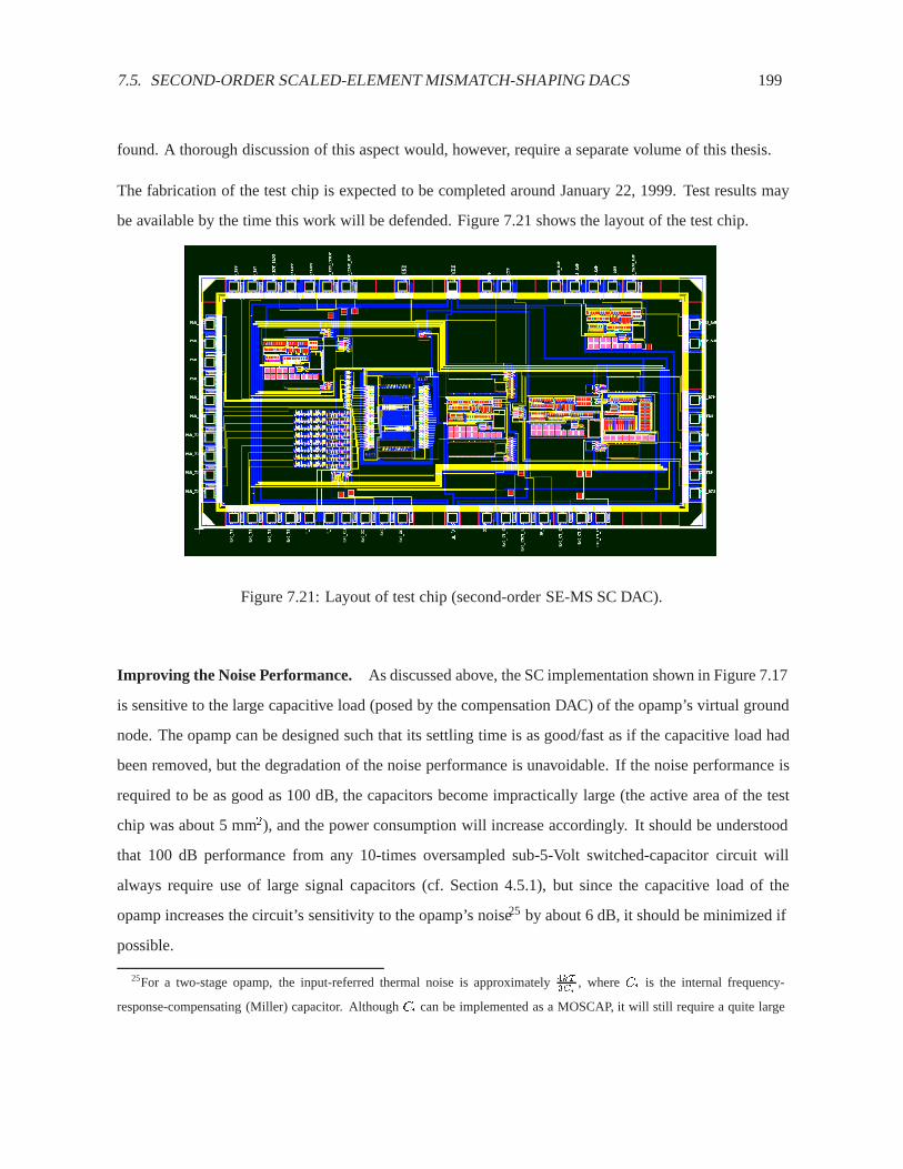
7.5. SECOND-ORDER SCALED-ELEMENT MISMATCH-SHAPING DACS 199
found. A thorough discussion of this aspect would, however, require a separate volume of this thesis.
The fabrication of the test chip is expected to be completed around January 22, 1999. Test results may
be available by the time this work will be defended. Figure 7.21 shows the layout of the test chip.
Figure 7.21: Layout of test chip (second-order SE-MS SC DAC).
Improving the Noise Performance. As discussed above, the SC implementation shown in Figure 7.17
is sensitive to the large capacitive load (posed by the compensation DAC) of the opamp’s virtual ground
node. The opamp can be designed such that its settling time is as good/fast as if the capacitive load had
been removed, but the degradation of the noise performance is unavoidable. If the noise performance is
required to be as good as 100 dB, the capacitors become impractically large (the active area of the test
chip was about 5 mm2), and the power consumption will increase accordingly. It should be understood
that 100 dB performance from any 10-times oversampled sub-5-Volt switched-capacitor circuit will
always require use of large signal capacitors (cf. Section 4.5.1), but since the capacitive load of the
opamp increases the circuit’s sensitivity to the opamp’s noise25 by about 6 dB, it should be minimized if
possible.
25For a two-stage opamp, the input-referred thermal noise is approximately 4kT3Ci
, where Ci is the internal frequency-
response-compensating (Miller) capacitor. Although Ci can be implemented as a MOSCAP, it will still require a quite large
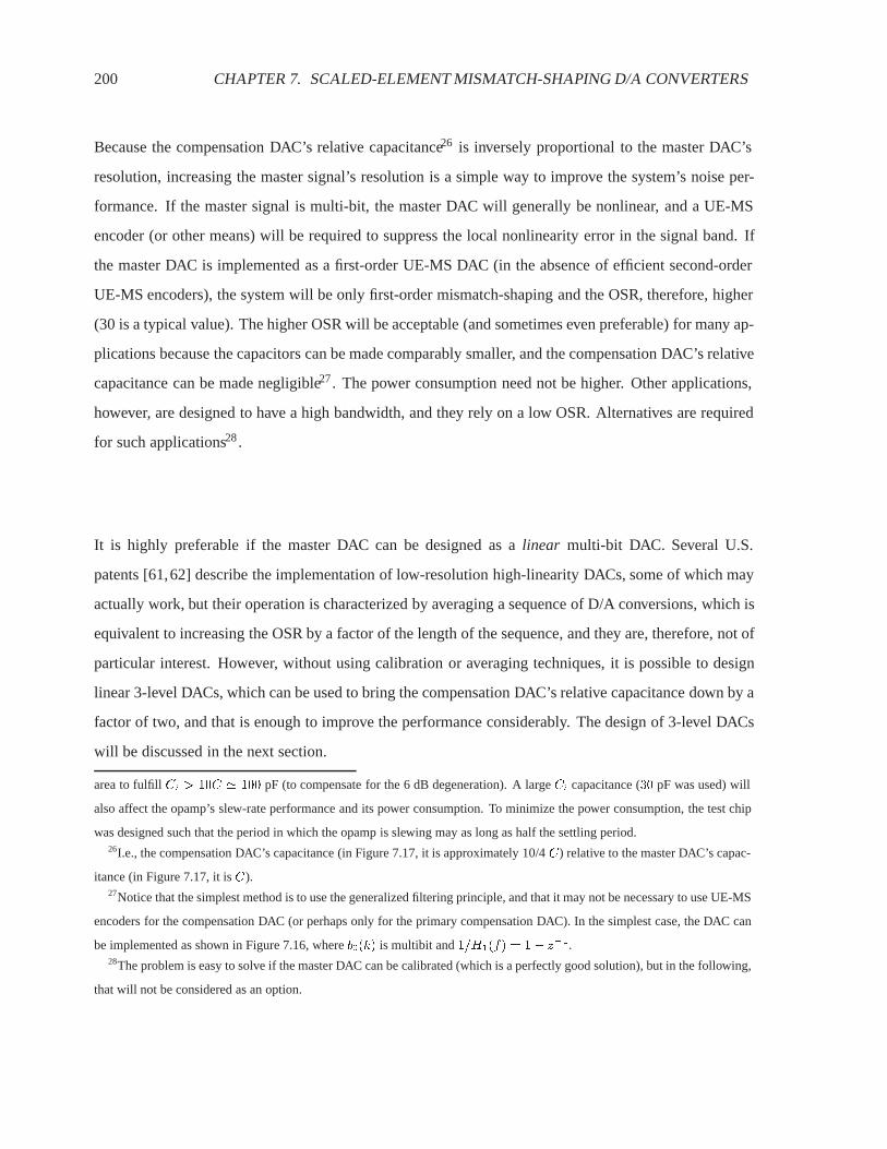
200 CHAPTER 7. SCALED-ELEMENT MISMATCH-SHAPING D/A CONVERTERS
Because the compensation DAC’s relative capacitance26 is inversely proportional to the master DAC’s
resolution, increasing the master signal’s resolution is a simple way to improve the system’s noise per-
formance. If the master signal is multi-bit, the master DAC will generally be nonlinear, and a UE-MS
encoder (or other means) will be required to suppress the local nonlinearity error in the signal band. If
the master DAC is implemented as a first-order UE-MS DAC (in the absence of efficient second-order
UE-MS encoders), the system will be only first-order mismatch-shaping and the OSR, therefore, higher
(30 is a typical value). The higher OSR will be acceptable (and sometimes even preferable) for many ap-
plications because the capacitors can be made comparably smaller, and the compensation DAC’s relative
capacitance can be made negligible27. The power consumption need not be higher. Other applications,
however, are designed to have a high bandwidth, and they rely on a low OSR. Alternatives are required
for such applications28 .
It is highly preferable if the master DAC can be designed as a linear multi-bit DAC. Several U.S.
patents [61,62] describe the implementation of low-resolution high-linearity DACs, some of which may
actually work, but their operation is characterized by averaging a sequence of D/A conversions, which is
equivalent to increasing the OSR by a factor of the length of the sequence, and they are, therefore, not of
particular interest. However, without using calibration or averaging techniques, it is possible to design
linear 3-level DACs, which can be used to bring the compensation DAC’s relative capacitance down by a
factor of two, and that is enough to improve the performance considerably. The design of 3-level DACs
will be discussed in the next section.
area to fulfill Ci > 10C ' 100 pF (to compensate for the 6 dB degeneration). A large Ci capacitance (30 pF was used) will
also affect the opamp’s slew-rate performance and its power consumption. To minimize the power consumption, the test chip
was designed such that the period in which the opamp is slewing may as long as half the settling period.26I.e., the compensation DAC’s capacitance (in Figure 7.17, it is approximately 10/4 C) relative to the master DAC’s capac-
itance (in Figure 7.17, it is C).27Notice that the simplest method is to use the generalized filtering principle, and that it may not be necessary to use UE-MS
encoders for the compensation DAC (or perhaps only for the primary compensation DAC). In the simplest case, the DAC can
be implemented as shown in Figure 7.16, where b0(k) is multibit and 1=H1(f) = 1� z�1.28The problem is easy to solve if the master DAC can be calibrated (which is a perfectly good solution), but in the following,
that will not be considered as an option.
7.5. SECOND-ORDER SCALED-ELEMENT MISMATCH-SHAPING DACS 201
7.5.5 Linear Three-Level DACs
Linear three-level DACs represent a variety of options to improve the discussed DAC designs. For
example, the minimalist filtering DAC (cf. Figure 7.10) can be implemented without UE-MS encoders29,
and so can the improved version shown in Figure 7.12 if the master signal is a two- or three-level signal.
As discussed above, 3-level DACs can also be used to improve the noise performance of the SC circuit
shown in Figure 7.17, and it will be discussed in the next section that they are very useful for current-
mode second-order mismatch-shaping DACs. Hence, linear 3-level DACs are important circuits.
Feasibility of 3-Level DACs. The basic operation/idea in 3-level DACs is very simple. In a fully-
differential circuit, an analog signal is dumped to either the positive path (conversion of “+1”), the
negative path (conversion of “�1”), or not at all (conversion of “0”).
An example of this principle is shown in Figure 7.22, which is from a paper presented by Ka Y. Leung
at ISSCC in 1997 [63]. The performance relies slightly on the matching of Cref;p and Cref;m and/or the
�2“+1”
“�1”
“�1”
“+1”“0”
�2
�2
“0”�1
�1
�1
�2
�2
+Vref
�Vref
�1 �2
VCM
Cref;p
Cint;p
Cref;m
Cint;m
Figure 7.22: Almost-linear 3-level DAC presented at ISSCC 1997.
matching of Cint;p and Cint;m, because it can be shown that the DAC’s output levels30 are proportional
29Academically, this is quite an interesting system, because it would implement a scaled-element mismatch-shaping DAC,
where each nominal output value could be generated in only two ways (one for each value of b0(k)). This is indeed a minimalist
mismatch-shaping DAC.30The DAC’s output is here the variation of the opamp’s output voltage, i.e., the signal is being integrated (which is generally

202 CHAPTER 7. SCALED-ELEMENT MISMATCH-SHAPING D/A CONVERTERS
to �1, 0, and +1 with a relative inaccuracy of
Ærel =
�Cref;p � Cref;m
Cref;p + Cref;m
��Cint;p � Cint;m
Cint;p + Cint;m
�(7.14)
However, assuming that the technology’s matching index is in the order of 0:1%, this error will not be
dominating unless the performance is 120 dB or better. The reported performance was “only” about
100 dB, but by means of calibration, the DAC was linearized to the 118 dB level. In this case, the error
sources are easy to identify: clock feedthrough and charge injection (charge errors) are well-known (and
quite large) “signals”, which will cause a signal-dependent error if the switches do not match perfectly
(and they never do). Another (larger) error results because the opamp’s offset only affects the output (by
Vo�setCrefCint
) in the samples that are either “+1” or “�1” (effectively, this moves the “0” away from the
DAC’s linear characteristic, and by adjusting the opamp’s offset, the DAC’s linearity can be adjusted).
Thermal-noise considerations were probably the reason why the circuit was designed this way.
Linear Three-Level DAC. Three-level DACs should preferably not rely on matching or cancellation
of any kind (in Figure 7.22, the assumed matching of the switches can cause nonlinearity), and certainly
not on the offset of opamps. Allowing the circuit to rely only on the second-order matching expressed
by Equation 7.14, a linear 3-level DAC can be implemented as shown in Figure 7.2331.
It is important that the Haigh-and-Singh delayed-clock-phases clocking scheme is used, i.e., that the
switches controlled by �1 and �2 are opened slightly before the switches controlled by �1d and �2d [29].
An alternative clocking scheme, which is equally good, is discussed in [64]. This clocking scheme may
provide a better understanding of the operation’s ideality.
Either clocking scheme will assure that it is only the switches controlled by �1 and �2 that will cause
charge errors. Because these switches are controlled independent of the digital signal, these charge errors
will not cause nonlinearity32 . As discussed in [64], the DAC’s output signal is determined exclusively
the case for �� quantizer front ends).31This implementation was proposed by Professor Un-Ku Moon (Oregon State University) during a private discussion. He
claims that it is used frequently in pipeline ADCs (which are one of his specialties).32The charge errors depend slightly on the surrounding impedance levels. This can potentially cause signal-dependent errors
(nonlinearity), but it can be brought to a very low level.
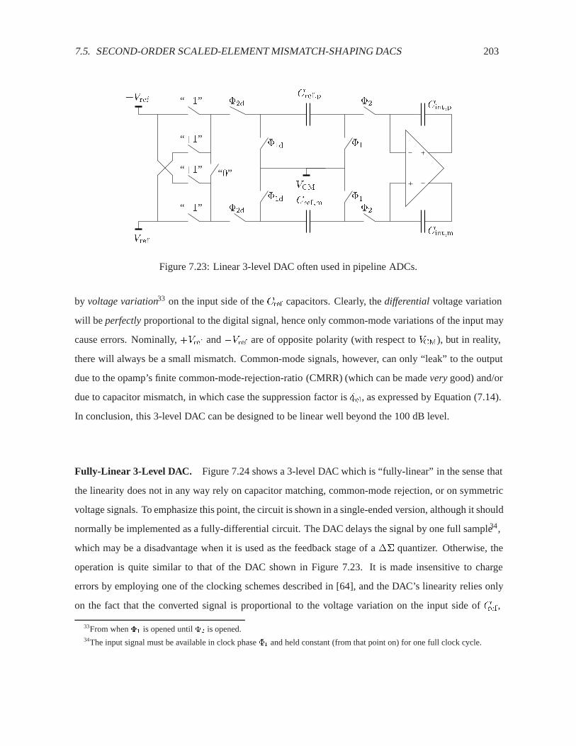
7.5. SECOND-ORDER SCALED-ELEMENT MISMATCH-SHAPING DACS 203
�2
�2
Cint;p
Cint;m
�1
�1
VCM
Cref;m
Cref;p
�2d
�2d
�1d
�1d
“0”
+Vref
�Vref
“�1”
“+1”
“+1”
“�1”
Figure 7.23: Linear 3-level DAC often used in pipeline ADCs.
by voltage variation33 on the input side of the Cref capacitors. Clearly, the differential voltage variation
will be perfectly proportional to the digital signal, hence only common-mode variations of the input may
cause errors. Nominally, +Vref and �Vref are of opposite polarity (with respect to VCM), but in reality,
there will always be a small mismatch. Common-mode signals, however, can only “leak” to the output
due to the opamp’s finite common-mode-rejection-ratio (CMRR) (which can be made very good) and/or
due to capacitor mismatch, in which case the suppression factor is Ærel, as expressed by Equation (7.14).
In conclusion, this 3-level DAC can be designed to be linear well beyond the 100 dB level.
Fully-Linear 3-Level DAC. Figure 7.24 shows a 3-level DAC which is “fully-linear” in the sense that
the linearity does not in any way rely on capacitor matching, common-mode rejection, or on symmetric
voltage signals. To emphasize this point, the circuit is shown in a single-ended version, although it should
normally be implemented as a fully-differential circuit. The DAC delays the signal by one full sample34,
which may be a disadvantage when it is used as the feedback stage of a �� quantizer. Otherwise, the
operation is quite similar to that of the DAC shown in Figure 7.23. It is made insensitive to charge
errors by employing one of the clocking schemes described in [64], and the DAC’s linearity relies only
on the fact that the converted signal is proportional to the voltage variation on the input side of Cref ,
33From when �1 is opened until �2 is opened.34The input signal must be available in clock phase �1 and held constant (from that point on) for one full clock cycle.
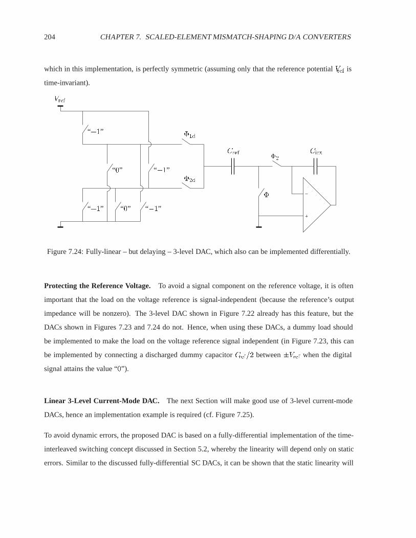
204 CHAPTER 7. SCALED-ELEMENT MISMATCH-SHAPING D/A CONVERTERS
which in this implementation, is perfectly symmetric (assuming only that the reference potential Vref is
time-invariant).
�2Cref
�1
�1d
Vref
�2d
“+1” “0” “�1”
“�1”“0”
“+1”
Cint
Figure 7.24: Fully-linear – but delaying – 3-level DAC, which also can be implemented differentially.
Protecting the Reference Voltage. To avoid a signal component on the reference voltage, it is often
important that the load on the voltage reference is signal-independent (because the reference’s output
impedance will be nonzero). The 3-level DAC shown in Figure 7.22 already has this feature, but the
DACs shown in Figures 7.23 and 7.24 do not. Hence, when using these DACs, a dummy load should
be implemented to make the load on the voltage reference signal independent (in Figure 7.23, this can
be implemented by connecting a discharged dummy capacitor Cref=2 between �Vref when the digital
signal attains the value “0”).
Linear 3-Level Current-Mode DAC. The next Section will make good use of 3-level current-mode
DACs, hence an implementation example is required (cf. Figure 7.25).
To avoid dynamic errors, the proposed DAC is based on a fully-differential implementation of the time-
interleaved switching concept discussed in Section 5.2, whereby the linearity will depend only on static
errors. Similar to the discussed fully-differential SC DACs, it can be shown that the static linearity will
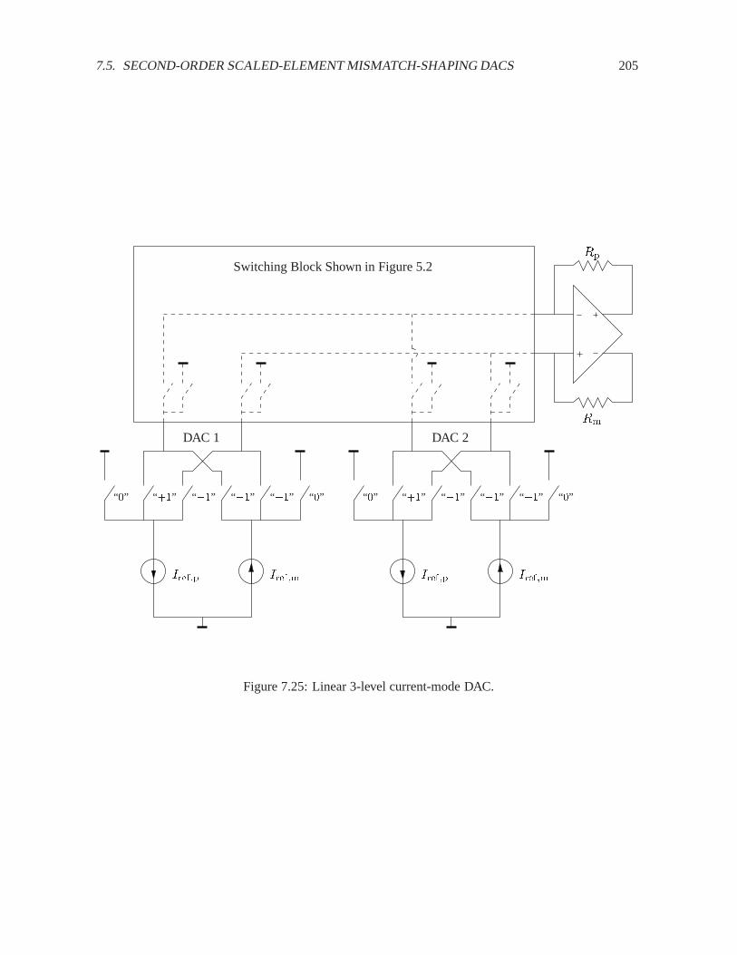
7.5. SECOND-ORDER SCALED-ELEMENT MISMATCH-SHAPING DACS 205
Iref;p Iref;m
“0” “+1” “�1” “�1” “+1” “0” “0” “+1” “�1” “�1” “+1” “0”
Rm
Rp
Switching Block Shown in Figure 5.2
Iref;p Iref;m
DAC 1 DAC 2
Figure 7.25: Linear 3-level current-mode DAC.

206 CHAPTER 7. SCALED-ELEMENT MISMATCH-SHAPING D/A CONVERTERS
be limited by
Ærel =
�Rp �Rm
Rp +Rm
��Iref;p � Iref;mIref;p + Iref;m
�(7.15)
If the resistors cannot be assured to match well, then the current sources must match accordingly better,
and vice versa. In general, to obtain 100 dB performance, Ærel must be less than �100 dB, which usually
is feasible.
Notice that the switching block’s impedance seen from the opamp is signal-dependent. This may cause
nonlinearity, because the opamp’s offset will affect the output as a linear function of this impedance.
The simplest way to alleviate the problem is to make the impedance level high, e.g., by cascode cou-
pling the reference current sources (the switches can be used for this purpose). As the ratio of the
opamp’s offset relative to full-scale output usually will be �40 dB or less, the reference current sources’
output impedance relative to the opamp’s feedback resistors need only be about 60 dB to obtain 100 dB
performance (usually feasible).
7.5.6 Current-Mode Implementation
Continuous-time current-mode DACs can typically be designed to have a better noise performance,
higher speed, and lower power consumption than their switched-capacitor counterparts. Hence, first-
order mismatch-shaping will generally be sufficient to obtain the required performance, but there may
be some applications where second-order mismatch shaping is preferable or needed.
Second-order mismatch-shaping DACs are best and simplest implemented using the generalized filtering
principle, e.g., as shown in Figure 7.15. However, the current-mode analog filters are not as simple to
implement as switched-capacitor circuits are (cf. Figure 7.17). The analog filters should, by definition,
match a discrete-time filter function, e.g., 1=H1(f) = 1� z�1; z = ej2�f=fs , but part of the advantage
of current-mode DACs is lost if switched-current filters are used. One option to avoid this scenario is to
design a CT filter
HCT(f) =
PQNi=0 bis
iPQDi=0 ais
i(7.16)

7.5. SECOND-ORDER SCALED-ELEMENT MISMATCH-SHAPING DACS 207
such that HCT(f) ' 1=H1(f) in the signal band; but it is typically difficult to obtain a reasonably good
matching of the filters, and even in the best case, the filters will not match in the entire frequency range35.
Another and typically much better option is to use pseudo-digital filters.
Pseudo-Digital Filters – Type I. Considering again the SC implementation shown in Figure 7.17, it
can be observed that each of the single-bit digital signals generated by the UE-MS encoders are D/A
converted and filtered individually by the non-reset capacitors. Hence, each capacitor can be construed
as a linear 3-level DAC converting the first-order difference of the respective single-bit digital signals.
The shown implementation is particularly suitable for SC circuits, but the underlying principle can also
be used for CT current-mode implementations, where the 3-level DACs are implemented differently.
This is shown in Figure 7.26, where the overall D/A conversion is performed by an array of 3-level
DACs36.
The spectral encoder (not shown) is assumed to be designed as a variation of the spectral encoder shown
in Figure 7.15, where the master signal b0(k) is of 3-level resolution, and the primary compensation
signal b1(k) is of only 2-bit resolution (because the magnitude of n0(k) is proportional to the master
signal’s step size, i.e., it is decreased by a factor of two). If the 3-level DACs are as linear as the
required performance, the composite DAC will perform second-order mismatch-shaping, and 100 dB
performance can be obtained at around 10 times oversampling.
Pseudo-Digital Filters – Type II. Figure 7.27 shows an alternative technique for the implementation
of pseudo-digital filters suitable for use in combination with the generalized filtering principle. For
simplicity, only the D/A conversion of one of the compensation signals is shown. Each of the two
single-bit signals from the UE-MS encoder is fed to a digital delay line, where each tap controls a linear
single-bit DAC. The filtering (second-order differentiation is shown) of these signals is perfectly linear.
35A filter will be needed to smoothen the DAC’s output signal36The system is assumed to be implemented as a fully-differential circuit, where the 3-level DACs are implemented as shown
in Figure 7.25. Notice that only one time-interleaving switching block (cf. Figure 5.2) should be implemented for the composite
DAC.

208 CHAPTER 7. SCALED-ELEMENT MISMATCH-SHAPING D/A CONVERTERS
1� z�1
1� z�1
1� z�1
1� z�1
2 levels
2 levels
2 levels
2 levels
@I0=2N
@I0=2N
b2(k)
b0(k)
b1(k)
b3(k)
bN�1(k)
2 levels
2 levels1� z�1
1� z�1
2 levels
1� z�1
1� z�1
3 levels
3 levels
3 levels
3 levels
2 levels
2 levels1� z�1
1� z�1
3 levels
3 levels
3 levels
3 levels
3 levels
2 bits
3 levels@I0
@I0=4
@I0=4
@I0=4
@I0=4
@I0=8
@I0=8
@I0=16
@I0=16
f(k)
3 levels
3 levels
2 levels
3 levels
3 levels
Figure 7.26: Continuous-time current-mode second-order mismatch-shaping DAC.

7.5. SECOND-ORDER SCALED-ELEMENT MISMATCH-SHAPING DACS 209
2 levels
2 levelsz�1
z�12 levels
2 levelsz�1
2 levelsz�1
2 levels
@I0=8
@I0=8
@�I0=4
@I0=8
@I0=8
@�I0=4
3 levelsb2(k)
c2(k)
Figure 7.27: Second-order differentiating compensation DAC.
Although each FIR filter individually is perfectly linear, this does not imply that the overall operation will
be ideal. If the FIR filter coefficients do not match their nominal value, the filter’s transfer function will
not be ideal, and the compensation of the master �� modulator’s truncation error �(k) (cf. Figure 7.2)
will not be ideal. Although mismatch of the filter’s transfer function can be tolerated to some extent (cf.
Section 7.5.2), this effect somewhat limits the maximum length of the FIR filter. First-order filters are
generally sufficient, but in this case the 3-level-DAC technique proposed above (Figure 7.26) is likely to
provide the best performance.
The analog-FIR filter technique is useful mainly if second-order filtering is required. In that case, the
numeric stability of the transfer function’s zeroes should be considered carefully. For example, the
two nominal zeroes at z = 1 for the circuit shown in Figure 7.27 are extremely sensitive to coefficient
inaccuracy (because it is a double zero), and the circuit should never be implemented as shown. The
filter matching can be improved either by designing the master �� modulator’s first filter stage as a
resonator (resonating at a high signal-band frequency), or by designing the second-order differentiation
as shown in Figure 7.28

210 CHAPTER 7. SCALED-ELEMENT MISMATCH-SHAPING D/A CONVERTERS
z�1
z�1
3 levels
@I0=8
@I0=8
3 levels
3 levels
3 levels
3 levelsb2(k)
1� z�1
1� z�12 levels
2 levels
c2(k)
@�I0=8
@�I0=8
Figure 7.28: Improved second-order differentiating compensation DAC.
7.5.7 Mismatch-Shaping Bandpass DACs
Bandpass unit-element mismatch-shaping encoders are feasible37 and it should be understood that all the
discussed techniques can be implemented as bandpass systems. Bandpass DACs are particularly simple
to implement when the center frequency is fs=4.
Notice, in particular, that the current-mode DAC shown in Figure 7.26 can be implemented as a bandpass
system because a single-bit signal, which is filtered by 1 + z�2, will result in a 3-level signal.
37For example, for tree-structure encoders, choose H(f) = 11+z�2
. Although the filter is of second order, the complexity,
stability and performance is equivalent to that of a first-order encoder.

Chapter 8
High-Resolution Delta-Sigma Quantizers
A general characteristic for state-of-the-art quantizers – and particularly for signal quantizers – is that
their performance is limited mainly by the linearity of an internal DAC (cf. Section 3.4 and Chapter 4).
However, with the development (and use) of scaled-element mismatch-shaping DACs (cf. Chapter 7),
other factors will typically turn out to be limiting in the design of a signal quantizer.
Consider, for example, Figure 8.1, which shows the topology in which most multi-bit �� quantizer’s
have been implemented thus far1. The loop quantizer may cause only little delay, hence it is practically
N-bit@1
KDAC
N-bit@1
1= bKDAC
e(k)g(k) v(k)H(f)
f(k)
d(k)Loop Quantizer
Feedback DAC
Figure 8.1: Traditional multi-bit delta-sigma quantizer.
always designed as a flash quantizer (cf. Section 3.4.1). Typically, to avoid complex circuitry and a high
1In the best case; quite often the feed-forward branch (from g(k) to the loop quantizer) is omitted and/or d(k) is injected at
internal nodes of H(f). These are undesirable variations that may cause substantial problems [43].
211
212 CHAPTER 8. HIGH-RESOLUTION DELTA-SIGMA QUANTIZERS
power consumption, the loop quantizer’s resolution, and hence the resolution of d(k), will be restricted
to less than (say) 5 bits. In other words, it is now the loop quantizer, and not the feedback DAC, which
is the limiting element2. This Chapter will consider some options for how the resolution of d(k) can be
increased without using high-speed high-resolution quantizers.
8.1 Choosing the Optimal Resolution
Consider Figure 8.1. An optimally designed signal quantizer will represent the analog input signal g(k)
by a high-resolution digital approximation d(k). It is, however, useless to increase the resolution of d(k)
beyond a certain limit. This limit is attained when the feedback DAC’s error signal m(k) dominates the
truncation error r(k)3
e(k) = g(k) � f(k) = [g(k) �KDACd(k)Truncation Error
]� [ m(k)DAC Error
] (8.1)
at which point the signal-to-noise ratio of e(k) is 0 dB, and there is only little information left for the
loop filter to detect. In other words, for a typical technology for which the relative matching index is
(say) 0.1%, the highest meaningful resolution of d(k) is in the order of 10 bits, in which case the analog
loop filter H(f) needs to be of only the same order as the mismatch-shaping DAC. Sometimes H(f)
may be designed one order higher to make the truncation error fully negligible.
The objective of this chapter is to design signal quantizers that provide an output signal d(k) with a
resolution of approximately 10 bits, without requiring use of high-speed high-resolution quantizers (to
minimize the quantizer’s complexity and power consumption).
2When the signal is represented with only 5-bit resolution, a sixth- or higher-order loop filter H(f) is required to obtain
100 dB performance at a OSR of 10 (cf. Section 3.4.3). If the signal is represented by (say) 10-bit resolution, a second-order
loop filter is sufficient.3Ideally, only the truncation error will be detected by H(f).

8.2. TWO-STAGE DELTA-SIGMA QUANTIZERS 213
8.1.1 Fundamental Principle for High-Resolution Quantization
High-resolution low-complexity quantizers generally function by adding the results from several low-
resolution quantizations of signals of very different effective magnitudes4. This fundamental principle
can also be used for the multi-bit �� quantizer shown in Figure 8.1.
In Section 4.3.1, it was derived that the magnitude of v(k) will be only a small factor of (say) 1 to 10
times larger than the loop quantizer’s step size. Hence, for high-resolution �� quantizers, the full-scale
range of g(k) will be significantly larger than that of v(k), whereby d(k) can possibly be generated as
the sum of a low-resolution quantization of g(k) (the MSBs of d(k)) and a low-resolution quantization
of v(k) (the LSBs of d(k)). This arrangement is shown in Figure 8.2. It can be construed as a digital-
domain implementation of the feed-forward path.
8.2 Two-Stage Delta-Sigma Quantizers
Figure 8.3 shows an alternative and very interesting interpretation of the circuit shown in Figure 8.2 (it
is the same circuit, but drawn differently), which will be called a two-stage �� quantizer. This Figure
clearly shows that the quantizer, in reality, is a two-stage residue-calculating quantizer (cf. Section 3.4.2),
where the first stage is a traditional residue stage (cf. Figure 3.17), and where the second stage is a ��
quantizer of the type shown in Figure 3.24. A peculiarity of this circuit is, however, that the two stages
share the same feedback DAC, which is essential in order to avoid unshaped DAC errors.
The�� quantizer’s input signal is the first stage’s residue signal r0(k) = g(k)�d0(k)KDAC. Preferably,
this residue signal should be added to v(k)5 (cf. Figure 8.4), but this would require that the loop quantizer
be clocked after the first-stage quantizer (timing issues are discussed later).
4For example, pipeline quantizers (cf. Figure 3.20).5In order to implement the �� quantizer in the preferred topology (cf. Section 3.4.3 and Figure 3.25).

214 CHAPTER 8. HIGH-RESOLUTION DELTA-SIGMA QUANTIZERS
9-bit@1
KDAC
5-bit@1
1= bKDAC
5-bit@16
1= bKDAC
e(k)g(k) v(k)H(f)
f(k)
d(k)
Feedback DAC
Loop Quantizer
d1(k)
d0(k)Coarse Quantizer
Figure 8.2: �� quantizer with a digital-domain feed-forward path.
5-bit@1
1= bKDAC
f(k)
Quant.Coarse
5-bit@16 9-bit@11= bKDAC KDAC
H(f)
Loop Quantizer
e(k)g(k)
�� Quantizer with input g(k)� d0(k)KDAC
Residue Stage
d1(k)
d(k)
d0(k)
v(k)
FeedbackDAC
Figure 8.3: The same �� quantizer as shown in Figure 8.2, but here drawn to emphasize its residue-
calculating topology.

8.2. TWO-STAGE DELTA-SIGMA QUANTIZERS 215
H(f)5-bit@1
1= bKDAC
f(k)
Quant.Coarse
5-bit@16 9-bit@11= bKDAC KDAC
d1(k)
d(k)
d0(k)
FeedbackDAC
g(k) e(k) v(k)
KDAC
5-bit@16
SimpleDAC
Loop Quantizer
Figure 8.4: Two-stage �� quantizer with implemented feed-forward path.
H(f)5-bit@1
1= bKDAC
Quant.Coarse
5-bit@161= bKDAC
f(k)
9-bit@1KDAC
d1(k)
d(k)
d0(k)
FeedbackDAC
e(k) v(k)Loop Quantizer
pdf[j(k)]
g(k)
j(k)
�8KDAC
Figure 8.5: Two-stage �� quantizer with fully-dithered first stage.
216 CHAPTER 8. HIGH-RESOLUTION DELTA-SIGMA QUANTIZERS
8.2.1 Preventing Nonlinearity
A perhaps not-so-obvious difference between the two-stage �� quantizers shown in Figures 8.3 and 8.4
is that the one without the feed-forward path is nonlinear, even if the feedback DAC and the two quantiz-
ers are ideal. The problem arises because the first stage (the residue stage) has a nonlinear static transfer
characteristic6 with unity gain, whereas the second stage (the �� quantizer) has a dynamic (frequency-
dependent) signal transfer function, which is unity only if the feed-forward path is implemented (cf.
Figure 8.4)7.
The nonlinearity can be avoided in two ways; either the two stages must be designed to have the same
signal transfer function, or the first stage must be made linear.
Matching the Transfer Functions. The signal transfer functions can be matched either by designing
the �� quantizer with the feed-forward path8, or by matching the first stage to the second by computing
d(k) as the sum of d1(k) and d0(k) filtered by H(f)1+H(f) . The latter technique, however, is of only limited
interest because it involves matching of analog/digital filters, and because the complexity of the digital
filter is considerable.
Linearizing the Residue Stage. Linearization of the residue stage is a matter of decorrelating the
residue signal from the input signal, which can be obtained by dithering the first-stage quantizer as
shown in Figure 8.5. The dither signal j(k) should preferably be white noise with a uniform probability-
density function (pdf) spanning one LSB of the first-stage quantizer. By identifying that this two-stage
�� quantizer is equivalent to the traditional multi-bit �� quantizer shown in Figure 8.1 (with a 9-bit
loop quantizer) where j(k) is added directly to v(k), linearity can be concluded. Notice, however, that
the dither signal j(k) is much larger than what would normally be used in a 9-bit �� quantizer, hence
the performance will not be comparable.
6Truncation to 5-bit resolution.7The signal transfer function is H(f)
1+H(f), which can differ substantially from unity when the OSR is low.
8In which case, the �� quantizer’s signal transfer function is 1+H(f)1+H(f)
= 1. See Section 3.4.3 and Equation (3.53).

8.2. TWO-STAGE DELTA-SIGMA QUANTIZERS 217
8.2.2 Simulation Results
The simulation results presented below are generated using an ideal feedback DAC. The actual (total)
error signal will be the sum of the shown truncation error signal and the feedback DAC’s error signal (cf.
Figure 3.22 and Chapter 7). The dashed line in the Figures shows an estimate of the feedback DAC’s
error signal, assuming that it is second-order shaped and that the technology’s matching index is 0:1%
(cf. Figure 7.18).
Reference Performance. Figure 8.6 shows the performance of a traditional multi-bit �� quantizer
with a 9-bit loop quantizer (cf. Figure 8.1). The loop filter is of third order and the NTFmax value is
three9. It can be observed that the truncation error signal dominates the feedback DAC’s error signal
in large parts of the frequency spectrum, but also that the DAC’s error signal limits the performance
at the target OSR (as it should for an optimally designed quantizer). The performance of this system
will represent the reference to which the performance of the proposed systems will be compared (the
performance cannot be improved unless a better DAC is available).
Performance of the Two-Stage Delta-Sigma Quantizer Shown in Figure 8.4. Figure 8.7 shows the
simulated performance of the two-stage �� quantizer shown in Figure 8.4. The performance of this
quantizer is virtually indistinguishable from the reference performance. This result is very encouraging,
because two-stage �� quantizers are significantly simpler to implement than traditional single-stage
single-loop multi-bit �� quantizers (cf. Section 8.3).
Performance of the Two-Stage Delta-Sigma Quantizers Shown in Figures 8.3 and 8.5. Figure 8.8
shows the performance of the two-stage �� quantizer shown in Figure 8.3. Clearly, this quantizer is
quite nonlinear (partly due to the high signal frequency), and hence it is not suitable for high-performance
9At 10 times oversampling, the signal-band power of the truncation error can be reduced by about 10 dB by increasing the
loop filter’s NTFmax value, but in this case there is little point in doing that, because the DAC’s error signal dominates the
signal-band performance and the out-of-band performance would be degraded. 100 dB performance cannot be obtained at 10
times oversampling when using a second-order loop (the resolution of d(k) is too low).

218 CHAPTER 8. HIGH-RESOLUTION DELTA-SIGMA QUANTIZERS
10−2
10−1
100
−150
−100
−50
0
10−2
10−1
100
−150
−100
−50
0
(a) Spectral power density versus frequency (b) Signal-band power versus 1/OSR
Output SignalTruncation Error Signal
DAC Error Signal
Figure 8.6: Traditional 9-bit �� quantizer (cf. Figure 8.1).
10−2
10−1
100
−150
−100
−50
0
10−2
10−1
100
−150
−100
−50
0
(a) Spectral power density versus frequency (b) Signal-band power versus 1/OSR
Output SignalTruncation Error Signal
DAC Error Signal
Figure 8.7: Two-stage �� quantizer with 5-bit quantizers and feed-forward signal path (cf. Figure 8.4).

8.3. IMPLEMENTATION OF TWO-STAGE DELTA-SIGMA QUANTIZERS 219
applications. The system can be linearized by dithering the first-stage quantizer, as shown in Figure 8.5,
in which case the performance will be as shown in Figure 8.9. Although this quantizer is linear, it is
observed that the performance does not measure up to the reference. The same performance can be
obtained using a traditional �� quantizer with a 5-bit loop quantizer, which often will be easier to
implement10.
Conclusion. The two-stage �� quantizer structure is very useful and efficient, but only if the feed-
forward signal path is implemented (as shown in Figure 8.4). In that case, the quantizer’s linearity
does not depend on the linearity of the first-stage quantization d0(k), which may be generated by actual
quantization of g(k), by prediction on the basis of recent values of d(k), or in almost any other way11.
For each bit of correlation between g(k) and d0(k), the Nyquist-band power of the truncation error signal
will decrease by 6 dB. Hence, in the ideal case, the first-stage quantizer would be a high-resolution
quantizer (say, a pipeline quantizer), such that the loop quantizer need have only a few bits of resolution.
However, this is only implementable if the required timing can be obtained (discussed in Section 8.3).
8.3 Implementation of Two-Stage Delta-Sigma Quantizers
As discussed in Section 3.4.3, the fundamental property of signal quantizers is that they attempt to
minimize the error signal e(k). In essence, the first stage of the two-stage �� quantizer (cf. Figure 8.3)
provides an estimate d0(k) of g(k), and the second stage generates d1(k) to correct for the inaccuracy of
the signal d(k) generated thus far (which is expressed by v(k)). If d0(k) is a good (say 10-bit accurate)
estimate of g(k), then e(k), v(k), and hence d1(k) will be small, and the loop quantizer can have a small
step size with only (say) 2 bits of resolution. On the other hand, if d0(k) is a less accurate (say, 5-bit)
10However, not always. Pipeline techniques will be proposed later, and then the first-stage (say pipeline) quantizer can be
designed to have a high resolution. For stability reasons (of the �� loop), the loop quantizer may have only little delay, hence
it generally cannot be designed as a pipeline quantizer.11A simple technique is to use linear prediction and define e.g. d0(k) = 2d(k � 1) � d(k � 2). Because the absolute
accuracy of linear prediction is best for small input signals, this technique will result in a system with a good dynamic range
performance. Consider also the predictive structure discussed in Section 9.3.1.
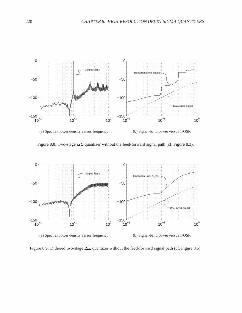
220 CHAPTER 8. HIGH-RESOLUTION DELTA-SIGMA QUANTIZERS
10−2
10−1
100
−150
−100
−50
0
10−2
10−1
100
−150
−100
−50
0
(a) Spectral power density versus frequency (b) Signal-band power versus 1/OSR
Truncation Error SignalOutput Signal
DAC Error Signal
Figure 8.8: Two-stage �� quantizer without the feed-forward signal path (cf. Figure 8.3).
10−2
10−1
100
−150
−100
−50
0
10−2
10−1
100
−150
−100
−50
0
(a) Spectral power density versus frequency (b) Signal-band power versus 1/OSR
Output SignalTruncation Error Signal
DAC Error Signal
Figure 8.9: Dithered two-stage �� quantizer without the feed-forward signal path (cf. Figure 8.5).

8.3. IMPLEMENTATION OF TWO-STAGE DELTA-SIGMA QUANTIZERS 221
estimate of g(k), then it is necessary to implement the �� quantizer’s feed-forward path to the loop
quantizer (cf. Figure 8.4), because otherwise, the estimation error g(k)�d0(k)KDAC will be transferred
directly to e(k), in which case v(k) will attain large values as an unmistakable sign of the less than ideal
operation.
Timing Problems. When thinking of the system in these terms, another problem becomes apparent.
Several operations must be performed sequentially and within one clock cycle12 to assure that g(k) and
f(k) are as correlated as possible in order to avoid e(k) and v(k) attaining large values. Clearly, this
poses a serious problem for high-speed systems because each operation takes time, thereby possibly lim-
iting the maximum sampling frequency. The problem becomes even worse if the feed-forward path need
be implemented, or if the first-stage quantizer is a multi-stage quantizer13 (continuous-time quantizers
are an all-together separate issue).
8.3.1 Introducing Pipeline Techniques to Allow Circuit Delays
As always, it is better to improve the system’s topology rather than blindly designing faster circuitry (to
which there always will be a limit, and which will be associated with an increased power consumption).
First, it is important to observe that it usually is tolerable if the two-stage �� quantizer is delaying, i.e.,
if d(k) represents, e.g., g(k � 2) and not necessarily g(k). Second, it should be observed that the main
objective is to avoid large values of e(k), which requires a high-resolution (10-bit) data14 quantization of
12The first-stage quantization of g(k), the addition of d0(k) and d1(k), the D/A conversion of d(k), and the subtraction of
g(k) and f(k).13Which, in reality, is two sides of the same problem. If the first-stage quantizer is a (say) two-step flash quantizer, the
resolution of d0(k) may be high enough to allow the feed-forward branch to be omitted. On the other hand, if the first-stage
quantizer is a single-stage flash quantizer, the resolution of d0(k) will be low and the feed-forward path required, in which case
the combined first-stage/loop quantizer operates as a two-stage flash quantizer.
Subranging quantizers may represent a good choice for the implementation of the first-state quantizer. Another technique,
which has a lot of potential, is to predict d0(k) on the basis of previous d(k) values. The calculations can typically be performed
in advance, whereby the feed-forward path is quite simple to implement. This approach is particularly interesting when the
input “g(k)” is a continuous-time signal (will be discussed).14The difference between data quantizers and signal quantizers is discussed in Section 3.4.
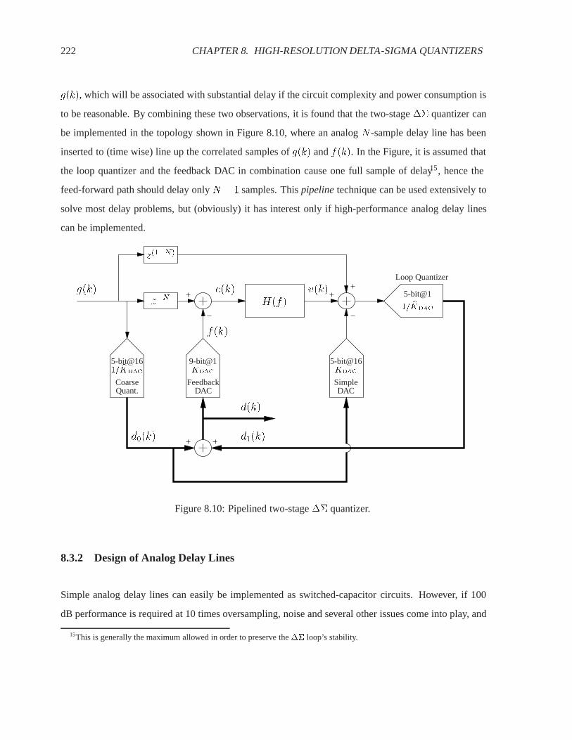
222 CHAPTER 8. HIGH-RESOLUTION DELTA-SIGMA QUANTIZERS
g(k), which will be associated with substantial delay if the circuit complexity and power consumption is
to be reasonable. By combining these two observations, it is found that the two-stage �� quantizer can
be implemented in the topology shown in Figure 8.10, where an analog N -sample delay line has been
inserted to (time wise) line up the correlated samples of g(k) and f(k). In the Figure, it is assumed that
the loop quantizer and the feedback DAC in combination cause one full sample of delay15, hence the
feed-forward path should delay only N � 1 samples. This pipeline technique can be used extensively to
solve most delay problems, but (obviously) it has interest only if high-performance analog delay lines
can be implemented.
H(f)5-bit@1
1= bKDAC
f(k)
Quant.Coarse
5-bit@16 9-bit@11= bKDAC KDAC
d1(k)
d(k)
d0(k)
FeedbackDAC
e(k) v(k)
KDAC
5-bit@16
SimpleDAC
Loop Quantizer
z�Ng(k)
z(1�N)
Figure 8.10: Pipelined two-stage �� quantizer.
8.3.2 Design of Analog Delay Lines
Simple analog delay lines can easily be implemented as switched-capacitor circuits. However, if 100
dB performance is required at 10 times oversampling, noise and several other issues come into play, and
15This is generally the maximum allowed in order to preserve the �� loop’s stability.

8.3. IMPLEMENTATION OF TWO-STAGE DELTA-SIGMA QUANTIZERS 223
then the circuit is not that simple to design.
The following discussion will consider the design of a high-performance switched-capacitor delay line,
which provides one full clock cycle of delay (and it can easily be extended). A one-sample delay is
usually sufficient because d(k) is required to be of only about 10-bit resolution. Half the delay can, for
example, be used for a two-step flash quantization, and the other half can be used for the mismatch-
shaping feedback DAC’s computations. A longer delay line will, however, be required if, for example,
the first-stage quantizer is designed as a pipeline quantizer.
Proposed Implementation: a Delay-Line Integrator. Figure 8.11 shows the proposed implementa-
tion, which is a delaying integrator, i.e., a combination of the one-sample delay line and the loop filter’s
first integrator stage.
The input voltage signal g(k) is sampled at the termination of clock phase �2. Capacitor C1 represents
the main (integrating) signal path. It dumps the signal charge qg(k) = �g(k)C1 to the integrating
capacitor Cint coupled across the main (high-performance) opamp OP1. The other (typically much
simpler) opamp, OP2, implements a sample-and-hold (S/H) operation. The input signal g(k) is sampled
on C3 in clock phases �2, and the capacitor is “flipped around” and used as the opamp’s feedback
element in clock phases �1. Capacitor C4 is used only to hold the output voltage while C3 samples the
next sample g(k+1) (uncritical operation, which may be incorporated to prevent undesired effects from
stray capacitors). The S/H stage drives C2 (of the same nominal value as C1) which in combination with
OP1 and Cint implements an inverting amplifier from g(k) to V1(k).
The fundamental idea is that qc(k) = (g(k)�g(k�1))C2 will cancel the signal charge qg(k) = �g(k)C1
from C1, hence g(k) will not affect V1(k) in the clock phase �1 immediately following the sampling
instance. However, in the following clock phase �1, the charge provided by C2 will be withdrawn
qc(k + 1) = (g(k + 1)� g(k))C2
= g(k + 1)C2 � g(k)C2 (8.2)
and the net result is that the signal �g(k)C1 is dumped to the feedback capacitor Cint one clock cycle
later than it otherwise would have been dumped (if OP2 is omitted). This delay provides the extra time
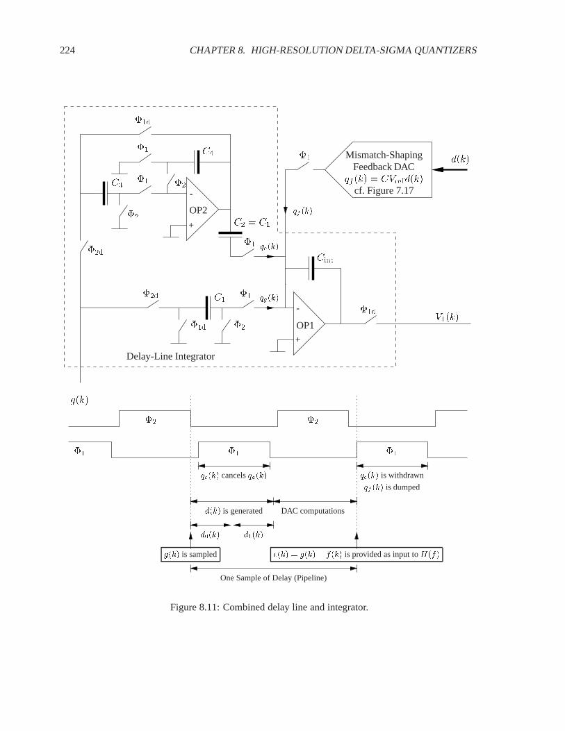
224 CHAPTER 8. HIGH-RESOLUTION DELTA-SIGMA QUANTIZERS
-
+
-
+
�1d
�1�2d
V1(k)
g(k)
Delay-Line Integrator
�2�1d
�1�2d
�1
OP1
qg(k)
qc(k)
Cint
C1
d(k)
qf (k)
C2 = C1
�1
�2OP2
C3 �2
�1d
�1 C4
�2
�1 �1 �1
�2
qc(k) cancels qg(k) qc(k) is withdrawn
qf (k) is dumped
d(k) is generated
g(k) is sampled
DAC computations
d1(k)d0(k)
e(k) = g(k)� f(k) is provided as input to H(f)
One Sample of Delay (Pipeline)
Mismatch-ShapingFeedback DAC
qf (k) = CVrefd(k)cf. Figure 7.17
Figure 8.11: Combined delay line and integrator.

8.3. IMPLEMENTATION OF TWO-STAGE DELTA-SIGMA QUANTIZERS 225
required for the generation of a high-resolution mismatch-shaped feedback signal qf (k) ' qg(k).
A key feature of this implementation is that it is quite robust with respect to circuit imperfections. Mis-
match of C1 and C2 will, e.g., cause only linear errors, and it is, therefore, of only little concern. Fur-
thermore, because C2 is not discharged at any time, all errors from OP2 (including noise, nonlinearity,
etc.) will be first-order differentiated; hence, C1 and OP1 will be the dominating error sources (which is
the best-case scenario16).
Figure 8.12 shows that the principle easily can be generalized and used for the implementation of delay
lines of arbitrary length.
-
+
z�1 z�1z�1 z�1
�1d
�2�1d
�1�2d
OP1
qg(k)
Cint
C1
�1 qc(k)
C2 = C1
�2d
V1(k)
g(k)
Figure 8.12: Generalized delay-line integrator with first-order shaped error signal.
8.3.3 Avoiding Sequential Settling
Figure 8.13 shows a more detailed (system-level) perspective of the pipelined two-stage �� quantizer
shown in Figure 8.10 (for N = 1). The loop filter H(f) has been sectioned in three parts to emphasize
the prospective use of the delaying integrator shown in Figure 8.11, and to show that the feed-forward
16For further noise improvements, C1 can be combined with the mismatch-shaping DAC’s master DAC.

226 CHAPTER 8. HIGH-RESOLUTION DELTA-SIGMA QUANTIZERS
path can be implemented without introducing new active elements (differentiation is a passive operation
in SC circuits).
The Problem. It is well understood that to preserve stability, the �� loop must have a path in its
topology that has exactly one sample of delay [1]. For the shown system topology, this implies that
F (z) will be nondelaying because the �� loop already includes one full sample of delay. For example,
to implement the classical second-order loop filter H(z) = z�1(2�z�1)(1�z�1)2
, the system should be designed
with F (z) = 2 � z�1, where “2” is the nondelaying part. This is not optimal, because nondelaying
SC circuits are subject to sequential settling, which will reduce the maximum sampling frequency [29].
To avoid this scenario, the topology can be modified to incorporate a local feedback path, as shown in
Figure 8.14.
The Proposed Solution. The gainA�KDAC of the local feedback DAC can always be chosen such that
the loop filter can be allowed to include one extra sample of delay, here emphasized by defining that the
middle part of the loop filter has the transfer function z�1J(z). For example, to implement the classical
second-order �� modulator, A must be 2 and J(z) = 1. It should be observed that, by introducing
the local feedback path, the �� quantizer’s input signal g(k)�K0KDAC is injected into the loop filter.
This effect is highly undesirable, and it should be compensated for by adjusting the feed-forward path as
shown [43]. Notice that, for A = 2, the feed-forward path’s transfer function becomes 1 + z�1, which
in fully-differential SC circuits can be implemented, e.g., by “switching” the two input capacitors in the
same way as for double-sampling SC circuits.
8.3.4 Proposed Circuit-Level Implementation
Figure 8.15 shows a detailed schematic for a switched-capacitor implementation of the pipelined two-
stage �� quantizer shown in Figure 8.14. For simplicity17, the �� loop is of only second order, and
it is designed to have the classical noise transfer function NTF(z) = (1 � z�1)2, which (as discussed
17As discussed above, the loop filter should preferably be of third order if the resolution of d(k) is only 9 bits.

8.3. IMPLEMENTATION OF TWO-STAGE DELTA-SIGMA QUANTIZERS 227
1
1� z�1
1� z�1
z�1
1� z�1
e(k)F (z)
d1(k)
g(k)
z�1=2
1� z�1
d0(k)
Feed-Forward Path
Delay-Line Integrator
Part of Loop FilterPart of Loop Filter
Part of Loop Filter
5-bit@16KDAC
First-Stage Quantizer
5-bit@161=KDAC
Loop Quantizer
5-bit@11=KDAC
SE-MS9-bit@1KDAC
1/2 Delay
�� Loop
d(k)
z�1=2
Figure 8.13: System-level implementation of the two-stage �� quantizer shown in Figure 8.10.
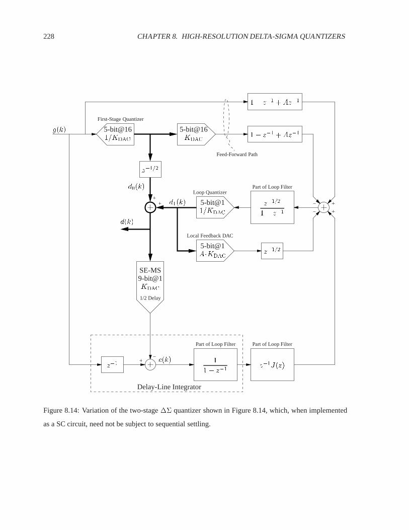
228 CHAPTER 8. HIGH-RESOLUTION DELTA-SIGMA QUANTIZERS
1
1� z�1z�1
z�1=2
z�1=2
e(k)z�1J(z)
d1(k)
g(k)
d0(k)
d(k)
Feed-Forward Path
Delay-Line Integrator
Part of Loop FilterPart of Loop Filter
Part of Loop Filter
5-bit@16KDAC
First-Stage Quantizer
5-bit@161=KDAC
Loop Quantizer
5-bit@11=KDAC
A�KDAC
5-bit@1
SE-MS9-bit@1KDAC
1/2 Delay
z�1=2
1� z�1
1� z�1 +Az�1
1� z�1 +Az�1
Local Feedback DAC
Figure 8.14: Variation of the two-stage �� quantizer shown in Figure 8.14, which, when implemented
as a SC circuit, need not be subject to sequential settling.

8.3. IMPLEMENTATION OF TWO-STAGE DELTA-SIGMA QUANTIZERS 229
- +
- +
- +
1/16
�
KDAC
5-bi
t@16
�1
d(k)
SE-M
SFe
edba
ckD
AC
KDAC
S2
Firs
tSta
geQ
uant
izer
5-bi
t@16
1=KDAC
5-bit@161=KDAC
5-bi
t@16
odd
even
g(k)
d1(k)
d0(k)
4C1
OP3
2C1
Loop Quantizer
S1
�1
2C1
Loc
alFe
edba
ckPa
th(A
=2
)
�1�
1
�2
�2
Del
ay-L
ine
Inte
grat
or
�2
�1
�1
�2
4C0
4C0
C0
OP1
OP2
�1
�2
�2
�1
�2
�1
�2
�
1
odd
KDAC
even
Feed
-For
war
dPa
th
even
odd
16C1
16C1
�1
V2(k)
V1(k)
16C1
16C1
Figure 8.15: SC implementation of the pipelined two-stage �� quantizer shown in Figure 8.14.

230 CHAPTER 8. HIGH-RESOLUTION DELTA-SIGMA QUANTIZERS
above) is obtained for J(z) = 1 and A = 2. Although the circuit is shown (pseudo) single-ended, it
should preferably be implemented as a fully-differential circuit.
The Schematic. The input stage is implemented as the delay-line integrator shown in Figure 8.11,
where also the used clock phases are shown. The first-stage (5-bit flash) quantizer is clocked when clock
phase �2 ends, and the result d0(k) is immediately D/A converted and subtracted from the S/H input
signal provided by OP2; the signal is represented as a charge pulse qFF(k) conducted by the feed-forward
path leading to OP3’s feedback capacitor. The feed-forward path is implemented pseudo differentially,
and it makes use of the switching technique commonly employed for differential double-sampling SC
circuits (the dashed lines indicate that the two connections are interchanged for every increment of k).
Hence, the feed-forward path will provide charge pulses of
qFF(k) = 16C1 ([g(k) + g(k � 1)]�KDAC[d0(k) + d0(k + 1)]) (8.3)
OP3 implements the loop filter’s second and last stage, and it also implements the summation of the feed-
forward signal qFF(k), the local feedback signal qLFB(k), and the signal from the loop filter’s previous
stage, OP1. These signals are represented as charge pulses dumped to the opamp’s virtual-ground node,
and they will cause a change in its output voltage V2(k). V2(k) represents mainly the residue from the
first-stage quantization, and it should be quantized as early as possible, i.e., as soon as V2(k) has settled
to 5-bit accuracy. Notice that to obtain 100 dB performance, OP3 must be allowed to settle to at least 10
– 12 bits accuracy; the loop quantizer, however, can be clocked earlier, because settling and truncation
errors will be compensated for in the following samples. In general, the loop quantizer can be clocked
approximately in the middle of clock phase �1 (see Figure 8.11), which will leave the feedback DAC
approximately the duration of clock phase �2 for computations necessary for the mismatch-shaping
operation.
Scaling Technique. The schematic (Figure 8.15) also shows a convenient scaling technique. Each of
the loop filter’s two stages amplifies the signal by a factor of four (not shown in Figure 8.14), which
implies that the two flash quantizers operate with the same LSB value. This is convenient, because (this

8.3. IMPLEMENTATION OF TWO-STAGE DELTA-SIGMA QUANTIZERS 231
way) they can be implemented by only one 5-bit flash quantizer multiplexed between the two functions
(they are not clocked simultaneously). The scaling technique also assures appropriate full-scale signal
levels, and suppression of device noise. Generally, C1 should be much smaller than C0 because its
thermal noise is suppressed by approximately 30 dB (when referred to the input, and for OSR = 10).

232 CHAPTER 8. HIGH-RESOLUTION DELTA-SIGMA QUANTIZERS

Chapter 9
Residue-Compensated Delta-Sigma
Quantizers
In Section 8.1 it was found that if the truncation error r(k) = g(k) � d(k)KDAC is to be dominated by
the feedback DAC’s error signal m(k), the input signal g(k) must be represented by a signal d(k) of at
least 10 bits of resolution1. Whereas the complexity of the feedback DAC is practically independent of
the resolution of d(k) (cf. Chapter 7), it was found that it may be difficult to quantize g(k) to the required
high (10-bit) resolution within the given time frame. Pipeline techniques were proposed as an efficient
means to alleviate this problem, but there may be situations (e.g., when designing continuous-time ��
quantizers) where this approach is not the most suitable.
Basic Operation of Residue-Compensated Delta-Sigma Quantizers. Now referring to Figure 8.1,
it may be observed that it is not a necessity that the truncation error r(k) be reduced to the same level
as that of the feedback DAC’s error signal m(k). If d(k) is a coarse representation of g(k) (i.e., if the
truncation error is substantial), it merely implies that there is significant2 information left in e(k) =
1As discussed in Section 4.3.1, 100 dB performance can be obtained even if the resolution of d(k) is as low as 3 to 4 bits;
but that involves the use of high-order (sixth to eighth order) loop filters, and there are several other reasons why this is not a
good design approach. When using a second-order loop filter, approximately 10 bits of resolution is required.2I.e., the signal-to-noise ratio (truncation-error to DAC-error ratio) is better than 0 dB (cf. page 212).
233

234 CHAPTER 9. RESIDUE-COMPENSATED DELTA-SIGMA QUANTIZERS
g(k) � f(k) = r(k) � m(k), and hence a better estimate dg(k) of g(k) can be obtained if e(k) is
quantized and the result de(k) is added to d(k)
dg(k) = d(k) + de(k) (9.1)
Signal quantizers that compensate for the main �� quantizer’s truncation error r(k) will be called
residue-compensated �� quantizers.
MASH quantizers (cf. Section 4.2), for example, are residue-compensated �� quantizers, but the way
they estimate e(k) is extremely sensitive to circuit imperfections (cf. Section 4.2.1). This Section will
focus on more robust ways to estimate e(k).
9.1 Directly Residue-Compensated Delta-Sigma Quantizers
Consider again the MASH structure shown in Figure 4.5. Things go wrong from the very beginning
because the signal dq(k), i.e., the estimate of q(k) upon which the estimate of e(k) is based, depends
on how well the two DACs match3. Preferably, de(k) should be the simplest possible function of e(k)
itself, and not some obscure reconstruction that depends on numerous parameters which are only poorly
controlled, e.g., matching of high-order analog and digital filters.
Figure 9.1 shows the simplest possible structure for residue-compensated �� quantizers, which will be
called directly residue-compensated �� quantizers.
9.1.1 Analysis and Performance Evaluation
The three data converters’ gains are all defined with respect to the same nominal value KDAC, but (as
always) there will be mismatch errors, etc.. Assume that the quantization de(k) of e(k) is associated
with an error signal y(k)
de(k) =1
KDAC2(e(k) + y(k)) (9.2)
3That this is not the dominating problem only emphasizes the poor robustness of the MASH topology.

9.1. DIRECTLY RESIDUE-COMPENSATED DELTA-SIGMA QUANTIZERS 235
H(f)g(k) e(k) d(k) dg(k)
de(k)
v(k)
f(k)
N-Bit@2P
1= bKDAC
KDAC1
N-Bit@2P
1=KDAC2
(P+1)-Bit@1
Residue Quantizer
Loop Quantizer
Feedback DAC
Figure 9.1: Directly residue-compensated �� quantizer.
which includes truncation, etc.. The residue-compensated �� quantizer’s output dg(k) can then be
calculated as
dg(k) = d(k) + de(k)
=[f(k)�m(k)]
KDAC1+
[e(k) + y(k)]
KDAC2
=[g(k) � e(k)�m(k)]
KDAC1+
[e(k) + y(k)]
KDAC2
=[g(k)]
KDAC1+[e(k)(1 � KDAC2
KDAC1)�m(k)KDAC2
KDAC1+ y(k)]
KDAC2(9.3)
Optimal Design. In Equation (9.3), the first term [g(k)]KDAC1
is the desired signal, and the second term
is the residue-compensated �� quantizer’s error signal. The error signal cannot possibly be made
smaller than m(k)KDAC1
, which is the performance that characterizes an optimally designed system. Hence,
in the ideal case and when implemented in a technology having a matching index of 0:1%, the residue-
compensated �� quantizer’s error signal will have a Nyquist-band power of around �60 dBFS (full-
scale), and the signal-band power will be around �100 dBFS at 10-times oversampling (cf. Figure 7.18).
Gain Errors. The factor (1�KDAC2KDAC1
) depends on the technology’s matching index, and it will typically
be in the order of �60 dB. If the �� quantizer is implemented with the feed-forward path and an N -bit

236 CHAPTER 9. RESIDUE-COMPENSATED DELTA-SIGMA QUANTIZERS
loop quantizer, the Nyquist-band power of e(k) will be in the order of
Pav[e(k)] = �6 dBFS � (N � 2) (9.4)
Hence, if the loop quantizer’s resolution is just a few (say, 3 to 5) bits, and the loop filter is of at least
second order, the gain-error signal e(k)(1�KDAC2KDAC1
) will not dominate at any frequency. In other words,
the performance will generally be limited only by the feedback DAC’s error signal m(k) and/or the
residue quantizer’s error signal y(k)4.
Nonlinearity Errors (Truncation). The Nyquist-band power of y(k) will generally depend on the
magnitude of e(k). If, for example, e(k) is �18 dBFS (realistic when using a 5-bit loop quantizer),
the target performance can be obtained if the residue quantizer is 13 to 14 bits linear. This level of
performance can just barely be obtained from data quantizers (cf. Section 3.4.2), but it can easily be
obtained when using signal quantizers (shown in Figure 9.2).
Dual-Loop Directly Residue-Compensated Delta-Sigma Quantizer. When analyzing the structure
shown in Figure 9.2, one finds that (because e(k) is small relative to full scale) H2(f) may be of lower
order than H(f), and also that the second feedback DAC need only be first-order mismatch-shaping.
The feed-forward path (the dashed line) should preferably be implemented (in which case it may make
sense to quantize e2(k) and add the result to the output), but even if this is not possible, the system will
yield a good performance. Notice that even if the two separate �� quantizers do not have the same
signal transfer function, harmonic distortion (similar to that shown in Figure 8.8) will not occur.
9.2 Indirectly Residue-Compensated Delta-Sigma Quantizers
Directly residue-compensated �� quantizers will not be discussed nor analyzed in great detail because
they are impractical to implement. The problem is that e(k) itself usually cannot be quantized, and
4The design of residue-compensated �� quantizers is equivalent to the design of the mismatch-shaping DACs discussed
in Section 7.1.1. m(k) and y(k) are local nonlinearity errors, and e(k)(1� KDAC2
KDAC1) is a gain error.
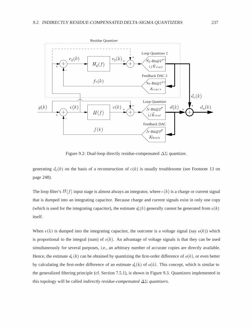
9.2. INDIRECTLY RESIDUE-COMPENSATED DELTA-SIGMA QUANTIZERS 237
H(f)
N2-Bit@2P2
1= bKDAC
KDAC2
N2-Bit@2P2
dg(k)
de(k)
g(k) e(k) d(k)v(k)
f(k)
N -Bit@2P
1= bKDAC
KDAC1
N -Bit@2P
Loop Quantizer
Feedback DAC
v2(k)
f2(k)
Loop Quantizer 2
Feedback DAC 2
e2(k)H2(f)
Residue Quantizer
Figure 9.2: Dual-loop directly residue-compensated �� quantizer.
generating de(k) on the basis of a reconstruction of e(k) is usually troublesome (see Footnote 13 on
page 248).
The loop filter’s H(f) input stage is almost always an integrator, where e(k) is a charge or current signal
that is dumped into an integrating capacitor. Because charge and current signals exist in only one copy
(which is used for the integrating capacitor), the estimate de(k) generally cannot be generated from e(k)
itself.
When e(k) is dumped into the integrating capacitor, the outcome is a voltage signal (say o(k)) which
is proportional to the integral (sum) of e(k). An advantage of voltage signals is that they can be used
simultaneously for several purposes, i.e., an arbitrary number of accurate copies are directly available.
Hence, the estimate de(k) can be obtained by quantizing the first-order difference of o(k), or even better
by calculating the first-order difference of an estimate do(k) of o(k). This concept, which is similar to
the generalized filtering principle (cf. Section 7.5.1), is shown in Figure 9.3. Quantizers implemented in
this topology will be called indirectly residue-compensated �� quantizers.

238 CHAPTER 9. RESIDUE-COMPENSATED DELTA-SIGMA QUANTIZERS
H1(f) H2(f)
Second-Stage
f(k)
N-Bit@2P
1= bKDAC
KDAC1
N-Bit@2P
Loop Quantizer
Feedback DAC
v(k)e(k) d(k)
o(k) de(k)
dg(k)
1=cH1(f)do(k)
1=KDAC2
(P+1)-Bit@1
Residue Quantizer
First-Stage
Residue Filter
g(k)
Figure 9.3: Indirectly residue-compensated �� quantizer.
9.2.1 Analysis and Performance Evaluation
The quantization do(k) of o(k) will be associated with an error signal (say, yo(k))
do(k) =o(k) + yo(k)
KDAC2(9.5)
Hence, the estimate de(k) of e(k) can be expressed as
de(k) = ch1�1(k) � do(k)=
ch1�1(k) � (o(k) + yo(k))
KDAC2
=ch1�1(k) � (h1(k) � e(k) + yo(k))
KDAC2
=e(k)
KDAC2+
[ch1�1(k) � h1(k)� 1] � e(k) +ch1�1(k) � yo(k)KDAC2
(9.6)
The first term in Equation (9.6) corresponds to e(k)KDAC2
in Equation (9.3), which was found to cause only
the nondominating gain error e(k)(1�KDAC2KDAC1
) in dg(k). The second term in Equation (9.6) corresponds
to y(k)KDAC2
in Equation (9.3), and it is, therefore, concluded that indirectly residue-compensated ��
quantizers are optimally designed when the feedback DAC’s error signal m(k) dominates
y(k) = [ch1�1(k) � h1(k)� 1] � e(k) +ch1�1(k) � yo(k)= ymatch(k) + yquan(k) (9.7)

9.2. INDIRECTLY RESIDUE-COMPENSATED DELTA-SIGMA QUANTIZERS 239
In Equation (9.7), the first error term ymatch(k) = [ch1�1(k) � h1(k) � 1] � e(k) is caused by mismatch
of the analog/digital filters, whereas the second error term yquan(k) =ch1�1(k) � yo(k) is caused by the
residue quantizer’s nonlinearity. The two terms will be considered separately.
9.2.2 Controlling the Residue-Quantization Error
If the residue quantizer is a data quantizer, then yo(k) will be a harmonic distortion of o(k). Because
o(k) is a “non-tonal” wide-band signal, yo(k) will be a white-noise-like error signal. Hence, assuming
that 1=H1(f) is a N th order differentiation, the signal-band power of yquan(k) can be estimated using
Figure 4.11.
For example, if 1=H1(f) is a first-order differentiation, the signal-band power of yquan(k) will be ap-
proximately 25 dB below the Nyquist-band power of yo(k) (at 10 times oversampling). In general, the
Nyquist-band power of yo(k) can be made at least 50 to 60 dB below full scale of o(k), which, for a 5-bit
loop quantizer, already will be about 20 dB below full-scale of g(k). In other words, it can easily be
assured that the Nyquist-band power of yo(k) is in the order of �70 dBFS to �80 dBFS. In conclusion,
if the residue quantizer is just 8 to 10 bit linear5 and 1=H1(f) is a first-order differentiation, the signal-
band power of yquan(k) will be approximately �95 to �105 dBFS (at OSR = 10, and when using a
5-bit loop quantizer).
If 1=H1(f) is (say) a second-order differentiation, yo(k) will be suppressed by an extra 12 dB (at OSR =
10), but since the magnitude of o(k) will increase, the overall improvement is only in the order of 6 dB.
Figure 9.4 shows the performance obtained (by simulation) when the residue quantizer is a 10-bit data
quantizer. The slight tonality is due to idle tones in e(k), but they can be avoided by dithering the ��
quantizer. The resolution of dg(k) is high (13 bit), which is reflected by the low Nyquist-band power of
yquan(k), but it is dominated by the feedback DAC’s error signal.
Using a Delta-Sigma Quantizer as the Residue Quantizer. Alternatively, the residue quantizer can
be designed as a �� quantizer. Then, the resolution of do(k) need not be as high as 8 nor 10 bits because
5Both the resolution and the linearity must be 8 to 10 bits.

240 CHAPTER 9. RESIDUE-COMPENSATED DELTA-SIGMA QUANTIZERS
10−2
10−1
100
−150
−100
−50
0
10−2
10−1
100
−150
−100
−50
0
(a) Spectral power density versus frequency (b) Signal-band power versus 1/OSR
Output Signal
yquan(k)
DAC Error Signal
Figure 9.4: Performance of the indirectly residue-compensated �� quantizer when the residue quantizer
is a 10-bit data quantizer.
the truncation error r2(k) = o(k)�do(k)KDAC2 ' yo(k) will be at least first-order shaped, and because
1=H1(f) will provide additional signal-band suppression of yo(k).
The simplest option is to design the residue quantizer as a first-order �� quantizer, e.g., as shown in
Figure 9.5. The two loop quantizers’ resolving ranges overlap by 1 bit, hence the resolution of the
output signal dg(k) is 9 bit. To illustrate the option (which is an important one, because it often makes
the circuit significantly simpler to implement6), the loop filter’s first stage is designed to be delaying.
Consequently, because the residue filter must be causal7, d(k) is delayed to align d(k) and de(k) time
wise8.
The main �� quantizer’s second loop filter stage can be of almost any order, but it should usually be
designed with a modest NTFmax value to prevent o(k) from attaining large values9.
6Timing issues become less of a concern because the delay “breaks” the row of sequential operations (the general pipeline
technique/idea). It is often preferable if the loop filter’s first stage delays e(k) by only one half clock cycle, because then, the
two loop quantizers can be implemented using only one multiplexed flash quantizer (as suggested in a previous example).7The residue filter cannot be made to implement 1�z�1
z�1= z � 1.
8This “trick” is also used when the residue quantizer is a pipeline quantizer.9There are, however, several design aspects in addition to that of preventing large values of o(k). Sometimes, higher
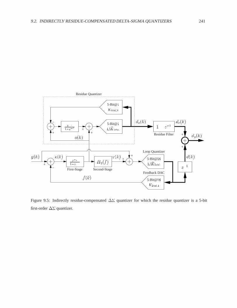
9.2. INDIRECTLY RESIDUE-COMPENSATED DELTA-SIGMA QUANTIZERS 241
z�1
1�z�1
H2(f)
Second-Stage
f(k)
5-Bit@16
1= bKDAC
KDAC1
Loop Quantizer
Feedback DAC
v(k)e(k)
First-Stage
g(k)z�1
1�z�1
5-Bit@16
o(k)
1� z�1
Residue Filter
de(k)
dg(k)
d(k)
z�1
5-Bit@1
KDAC2
5-Bit@1
1= bKDAC
Residue Quantizer
do(k)
Figure 9.5: Indirectly residue-compensated �� quantizer for which the residue quantizer is a 5-bit
first-order �� quantizer.

242 CHAPTER 9. RESIDUE-COMPENSATED DELTA-SIGMA QUANTIZERS
Simulation Results. Figure 9.6 shows the performance obtained (by simulation) when the main ��
quantizer’s loop filter is of second order with NTFmax = 1:5. It can be observed that this system is not
optimally designed because yquan(k) dominates the DAC’s error signal. This is because the resolution
of dg(k) is only 9 bits, and because the truncation error is only second-order shaped (furthermore, the
residue quantizer had to be dithered to avoid idle tones.
10−2
10−1
100
−150
−100
−50
0
10−2
10−1
100
−150
−100
−50
0
(a) Spectral power density versus frequency (b) Signal-band power versus 1/OSR
Output Signal
DAC Error Signal
yquan(k)
Figure 9.6: Performance of the indirectly residue-compensated �� quantizer shown in Figure 9.5.
To improve the signal-band performance, the system was also simulated for a design where the residue
quantizer is a �� quantizer with a second-order loop filter. The loop filter was designed with a high
NTFmax value (almost 4), and it was designed to resonate at a high signal-band frequency10 to efficiently
reduce the signal-band power of the residue quantizer’s truncation error. The performance obtained (by
simulation) from this system is shown in Figure 9.7. Now, the signal-band performance is dominated
by the DAC’s error signal (optimal design), but the error signal’s Nyquist-band power is still fairly large
due to the “low” resolution of dg(k) and to the aggressive design of the residue quantizer’s loop filter.
NTFmax values will be chosen (even as high as 4 or 6) to reduce the gain error’s e(k)(1 � KDAC2
KDAC1) signal-band power by
shaping e(k) efficiently (cf. Equation 9.3). The tradeoff is that the residue quantizer must have a larger resolving range, in
which case it makes good sense to design the residue quantizer as an indirectly residue-compensated �� quantizer (recursive
use).10More precisely, the loop filter was designed according to Figure 4.4, where 1 = 0:0736.
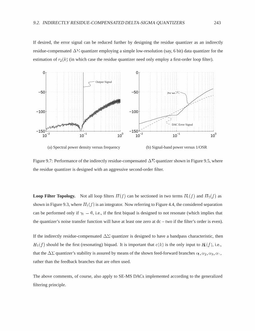
9.2. INDIRECTLY RESIDUE-COMPENSATED DELTA-SIGMA QUANTIZERS 243
If desired, the error signal can be reduced further by designing the residue quantizer as an indirectly
residue-compensated �� quantizer employing a simple low-resolution (say, 6 bit) data quantizer for the
estimation of r2(k) (in which case the residue quantizer need only employ a first-order loop filter).
10−2
10−1
100
−150
−100
−50
0
10−2
10−1
100
−150
−100
−50
0
(a) Spectral power density versus frequency (b) Signal-band power versus 1/OSR
Output Signal
yquan(k)
DAC Error Signal
Figure 9.7: Performance of the indirectly residue-compensated �� quantizer shown in Figure 9.5, where
the residue quantizer is designed with an aggressive second-order filter.
Loop Filter Topology. Not all loop filters H(f) can be sectioned in two terms H1(f) and H2(f) as
shown in Figure 9.3, whereH1(f) is an integrator. Now referring to Figure 4.4, the considered separation
can be performed only if 1 = 0, i.e., if the first biquad is designed to not resonate (which implies that
the quantizer’s noise transfer function will have at least one zero at dc – two if the filter’s order is even).
If the indirectly residue-compensated �� quantizer is designed to have a bandpass characteristic, then
H1(f) should be the first (resonating) biquad. It is important that e(k) is the only input to H1(f), i.e.,
that the �� quantizer’s stability is assured by means of the shown feed-forward branches �1; �2; �3; �4,
rather than the feedback branches that are often used.
The above comments, of course, also apply to SE-MS DACs implemented according to the generalized
filtering principle.
244 CHAPTER 9. RESIDUE-COMPENSATED DELTA-SIGMA QUANTIZERS
9.2.3 Controlling the Filter-Mismatch-Induced Error
Residue-compensated �� quantizers implemented in the MASH topology are extremely sensitive to
filter-mismatch-induced errors, which often limits the performance considerably (cf. Section 4.2.1). An
important advantage of the proposed indirectly residue-compensated �� quantizers (cf. Figure 9.3) is
that they are much more robust with respect to such errors. The following discussion will analyze this
aspect.
Calculating the Error’s Spectral Composition. The filter-mismatch-induced error ymatch(k) was
found to be (cf. Equation (9.7))
ymatch(k) = [ch1�1(k) � h1(k)� 1] � e(k) (9.8)
where ch1�1(k) and h1(k) are the impulse responses of 1=cH1(f) and H1(f), respectively. In other
words, ymatch(k) can be considered as being generated by filtering e(k) with the filter
Hmatch(f) =
H1(f)cH1(f)
� 1
!(9.9)
The spectral composition of e(k) will be modeled as a white-noise signal11 q(k) $ Q(f) filtered by
the �� quantizer’s noise transfer function NTF(f) = 11+H1(f)H2(f)
. Hence, the spectral composition of
ymatch(k)$ Ymatch(f) can be calculated from
Ymatch(f) = Hmatch(f) � NTF(f) �Q(f) (9.10)
Equation (9.10) shows that the loop quantizer’s truncation error q(k)will be suppressed by bothHmatch(f)
and NTF(f); Hmatch(f) expresses suppression due to the residue-compensation process, whereas NTF(f)
expresses suppression obtained by noise shaping.
11As discussed in Section 4.1.1, the white-noise assumption for q(k) can be hard to justify. However, since the validity of
this discussion does not depend on the (lack of) autocorrelation of q(k), the model has been allowed for simplicity. If the
multi-bit �� quantizer is dithered, the model is fully justifiable.

9.2. INDIRECTLY RESIDUE-COMPENSATED DELTA-SIGMA QUANTIZERS 245
Estimation of the Mismatch FactorHmatch(f). When H1(f) is a simple filter function, Hmatch(f)
can be estimated qualitatively. The following discussion will consider the typical case where H1(f)
nominally is a first-order integrator, i.e., cH1(f) =1
1�z�1(it is irrelevant whether or not the integrator
delays e(k)).
The transfer function of a switched-capacitor integrator based on a linear opamp with finite-gain is [29]
H1 =1
1� (1� �)z�1(9.11)
where � is the reciprocal of the opamp’s gain (� is typically in the range from �40 to �100 dB).
Hmatch(f) can then be calculated from
Hmatch(f) =1� z�1
1� (1� �)z�1� 1
=1� z�1 � 1 + (1� �)z�1
1� (1� �)z�1
=��z�1
1� (1� �)z�1(9.12)
The frequency response (magnitude) of Hmatch(f) is shown in Figure 9.8 for a select set of � values. It
can be observed that Hmatch(f) is a first-order low-pass filter with 0 dB gain at 0 Hz and approximately
�6 dB + 20 log10(�) dB gain at the Nyquist frequency.
When using this estimate to evaluate the expression for Ymatch(f) in Equation (9.10), the following
observations can be made:
� For a first-order �� quantizer with NTF(f) = (1 � z�1), the frequency dependence of the two
transfer functions Hmatch(f) and NTF(f) will cancel almost perfectly, i.e, Ymatch(f) ' �Q(f).
Thus, Ymatch(f) will be a small white-noise-like error signal for which the Nyquist-band power is
inversely proportional to the loop quantizer’s resolution and the opamp gain.
Simulations show that to obtain 100 dB performance at OSR = 10, the opamp gain must be at
least 91 dB�N � 6 dB, where N is the loop quantizer’s resolution.
� If the opamp gain is low, i.e., if the filters H1(f) and 1=cH1(f) match poorly, the loop filter’s order
and/or NTFmax value can be increased to suppress Ymatch(f) by means of NTF(f). As discussed

246 CHAPTER 9. RESIDUE-COMPENSATED DELTA-SIGMA QUANTIZERS
10−3
10−2
10−1
100
−120
−100
−80
−60
−40
−20
0
� = �100 dB
� = �80 dB
� = �60 dB
� = �40 dB
jHmatch(f)j
f=2fs
dB
� = �20 dB
Figure 9.8: The magnitude response of Hmatch(f) when H1(f) is a first-order integration. � is the
integration’s relative “leakage”.
on page 243, NTF(f) will (for baseband systems) always have a zero at 0 Hz. This zero will
cancel the pole in Hmatch(f), and the remaining poles and zeroes in NTF(f) will characterize the
spectral composition of Ymatch(f). If, for example, NTF(f) is of second order, Ymatch(f) will be
first-order shaped. Some important details are discussed below.
Evaluation. The filter-mismatch-induced error signal ymatch(k) will only rarely be a problem because
it is a white-noise signal q(k) filtered by a blocking filter NTF(f)Hmatch(f), i.e., the high-pass filter
NTF(f) is followed by the low-pass filter Hmatch(f).
The error signal ymatch(k) can be suppressed in many ways. Because the power of q(k) is proportional
to the loop quantizer’s resolution, the attenuation required of the blocking filter NTF(f)Hmatch(f) is
reduced as the resolution of d(k) is increased. For example, by increasing the loop quantizer’s resolution
from 1 to 5 bits, the attenuation required from NTF(f)Hmatch(f) is reduced by 24 dB.
The low-pass filter’s Hmatch(f) frequency response depends on stochastic processes, and it cannot be
designed directly. However, the filter’s maximum gain is always 0 dB, and the cutoff frequency and the
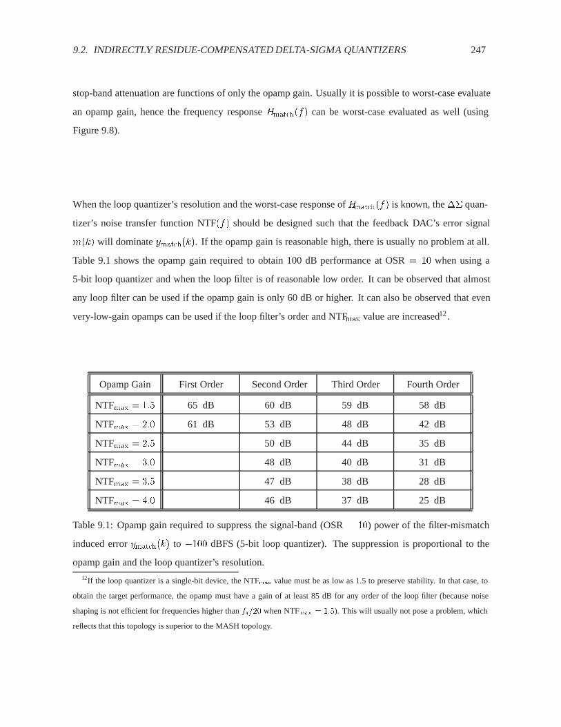
9.2. INDIRECTLY RESIDUE-COMPENSATED DELTA-SIGMA QUANTIZERS 247
stop-band attenuation are functions of only the opamp gain. Usually it is possible to worst-case evaluate
an opamp gain, hence the frequency response Hmatch(f) can be worst-case evaluated as well (using
Figure 9.8).
When the loop quantizer’s resolution and the worst-case response of Hmatch(f) is known, the �� quan-
tizer’s noise transfer function NTF(f) should be designed such that the feedback DAC’s error signal
m(k) will dominate ymatch(k). If the opamp gain is reasonable high, there is usually no problem at all.
Table 9.1 shows the opamp gain required to obtain 100 dB performance at OSR = 10 when using a
5-bit loop quantizer and when the loop filter is of reasonable low order. It can be observed that almost
any loop filter can be used if the opamp gain is only 60 dB or higher. It can also be observed that even
very-low-gain opamps can be used if the loop filter’s order and NTFmax value are increased12.
Opamp Gain First Order Second Order Third Order Fourth Order
NTFmax = 1:5 65 dB 60 dB 59 dB 58 dB
NTFmax = 2:0 61 dB 53 dB 48 dB 42 dB
NTFmax = 2:5 50 dB 44 dB 35 dB
NTFmax = 3:0 48 dB 40 dB 31 dB
NTFmax = 3:5 47 dB 38 dB 28 dB
NTFmax = 4:0 46 dB 37 dB 25 dB
Table 9.1: Opamp gain required to suppress the signal-band (OSR = 10) power of the filter-mismatch
induced error ymatch(k) to �100 dBFS (5-bit loop quantizer). The suppression is proportional to the
opamp gain and the loop quantizer’s resolution.
12If the loop quantizer is a single-bit device, the NTFmax value must be as low as 1.5 to preserve stability. In that case, to
obtain the target performance, the opamp must have a gain of at least 85 dB for any order of the loop filter (because noise
shaping is not efficient for frequencies higher than fs=20 when NTFmax = 1:5). This will usually not pose a problem, which
reflects that this topology is superior to the MASH topology.

248 CHAPTER 9. RESIDUE-COMPENSATED DELTA-SIGMA QUANTIZERS
9.2.4 Designing Residue-Compensated Delta-Sigma Quantizers
Residue-compensated quantizers are best implemented in the topology shown in Figure 9.3. The reso-
lution of the output dg(k) should preferably be fairly high (say, 8 to 10 bits or more) to avoid that dg(k)
includes high-order shaped error signals (to avoid a requirement for complex digital filters). For this and
several other reasons, the loop quantizer’s resolution should not be too low – 4 to 5 bits seems to be a
good choice.
Designing the Loop Filter. To avoid dominating filter-mismatch errors, the loop filter’s first stage
should be simple. Since H1(f) = 1 usually is not practical13; a first-order integrator is the preferred
choice for baseband quantizers. If the opamp gain is sufficiently high (cf. Table 9.1), filter-mismatch
errors need not be considered when designing the loop filter’s second stage. The loop filter H1(f)H2(f)
should instead be designed such that the gain-mismatch error e(k)(1�KDAC2KDAC1
) is sufficiently suppressed.
The factor (1 � KDAC2KDAC1
) can usually be made small (say, �50 to �60 dB). Since the power of e(k) is
13 It may not be the simplest option, but very good systems can indeed be designed if e(k) is reconstructed and quantized by
the residue quantizer. This option is illustrated below. The main reconstruction DAC (DAC3) takes the place of the main ��
quantizer’s feedback DAC (DAC1) as the system’s most critical element. Hence, DAC3 and possibly also DAC2 should be
mismatch-shaping, whereas DAC1 need not be mismatch-shaping. A key point is thatKDAC3 need not match KDAC1 perfectly
because mismatch will cause an error which is proportional to g(k) (a linear error). The topology is particularly useful for
bandpass quantizers, where designing H1(f) = z�1
1+z�2may be associated with an intolerable large filter-mismatch-induced
error. Hence, on occasion, the circuit’s higher complexity may be well worth while.
H(f)
KDAC1
1=cKDAC
cKDACKDAC3
KDAC2
1=cKDAC
g(k)
H2(f)
dg(k)
Residue Quantizer
9.2. INDIRECTLY RESIDUE-COMPENSATED DELTA-SIGMA QUANTIZERS 249
inversely proportional to the loop quantizer’s resolution, it is usually sufficient that NTF(f) suppresses
q(k) (in the signal-band) by as little as 20 to 30 dB when using a 5-bit loop quantizer. This can be
obtained with a second order loop filter. If the loop quantizer’s resolution is low, and/or if (1�KDAC2KDAC1
) is
considerably higher than �50 dB, the loop filter should be of higher (say, third or fourth) order and the
NTFmax value should be increased (to say, 3 or 4), in which case the residue quantizer must be designed
with a wider resolving range.
Designing the Residue Quantizer. The residue quantizer’s step size must be small enough to assure
that dg(k) has the required resolution. For example, to obtain 9-bit resolution of dg(k) when using a
5-bit loop quantizer, the resolution of do(k) must be at least 5 bits. If the loop filter H1(f)H2(f) is
designed with a high NTFmax value, the resolution of do(k) must be higher.
Considering that 1=H1(f) is a first-order high-pass filter, o(k) cannot be quantized directly (with a
data quantizer) to the discussed minimum resolution of do(k). If that is done, the residue quantizer’s
truncation error will cause a dominating error in dg(k). This problem can be avoided either by increasing
the resolution of do(k) using a higher-resolution data quantizer or by shaping the truncation error by
using a �� quantizer.
If the residue quantizer is designed as a data quantizer, the truncation error will be suppressed by only
about 24 dB (at OSR = 10, cf. Figure 4.11), hence the resolution of dg(k) must be at least 12 bits.
Hence, if the loop quantizer’s resolution is (say) 5 bits, the residue quantizer’s resolution must be at least
8 or 9 bits. The residue quantizer can, for example, be implemented as a pipeline quantizer, in which
case d(k) must be delayed accordingly before it is added to de(k) (cf. Figure 9.5).
If the residue quantizer is designed as a �� quantizer, the truncation error can be efficiently shaped,
and the resolution of do(k) can be as low as the discussed minimum. If the resolution of d(k) and
do(k) are both 5 bits, the residue quantizer should be of at least second order (see Figures 9.6 and 9.7).
A better/simpler option is to design the residue quantizer as an indirectly residue-compensated ��
quantizer with a first-order loop filter and with a low-resolution data quantizer as the (internal) residue
quantizer14.
14A simple design would use a second-order main loop filter, a 4-bit loop quantizer for d(k), and generate do(k) as a 4-bit
250 CHAPTER 9. RESIDUE-COMPENSATED DELTA-SIGMA QUANTIZERS
Timing the System. An important advantage of indirectly residue-compensated �� quantizers is that
they can easily be pipelined – simply by making H1(f) delaying by one half of a full clock cycle. An
example was shown in Figure 9.5, but the concept can be generalized and used throughout the structure
(this is especially convenient when the residue quantizer incorporates a pipeline data quantizer).
Conclusion. The conclusion is good. Very robust high-performance signal quantizers can be imple-
mented in the described topologies, and the circuit complexity is modest. Many variations are possible;
the topology can be tailored to suit almost any need.
9.3 Continuous-Time Delta-Sigma Quantizers
As discussed in Section 4.5.2, continuous-time �� quantizers can be designed to yield a better per-
formance than their discrete-time counterparts. However, they are generally more difficult to design
because dynamic errors and circuit timing are tricky issues. This section will consider some of the new
and interesting design options that are available when using the techniques described in this chapter and
in Chapter 8.
9.3.1 High-Resolution Continuous-Time Delta-Sigma Quantizers
Consider Figure 4.19. As discussed above, e(t) should preferably be made as small as possible. There
is, however, a limit to how small e(t) can be made, and this limit is independent of how well the system
is designed. The problem is that the feedback signal fh(t) is constant for an entire clock cycle, whereas
the input signal g(t) varies continuously. If g(t) is only 10 times oversampled, e(t) may attain values
noise-shaped representation of o(k), which is compensated with a 4-bit-differentiated (which results in a 5-bit) representation
of the truncation. This way, the resolution of dg(k) will be around 10 bits, and the errors will all be small and second-
order shaped. The main feedback DAC must (of course) be second-order mismatch-shaping, but the residue quantizer need
only employ a first-order mismatch-shaping feedback DAC. In fact, the residue quantizer’s feedback DAC may not need to
be mismatch-shaping because o(k) is small, and all errors (including the DAC error) in do(k) will be first-order shaped by
1=cH1(f).

9.3. CONTINUOUS-TIME DELTA-SIGMA QUANTIZERS 251
that are as large as one third of full scale; absolutely nothing can be done to prevent that. This is not
even the worst case because g(t) may not have been processed by an anti-aliasing filter (this option was
emphasized as an advantage of CT �� quantizers), hence the “sample-to-sample” variation of g(t) may
be substantial.
To understand the complexity of designing high-resolution CT �� quantizers, it should be observed
that the feedback DAC usually will be delaying, partly because the spectral encoder will cause delay,
and partly because it may be necessary to employ a delaying switching scheme to prevent dynamic
DAC errors (cf. Chapter 5 and Figure 5.2). Hence, to minimize the magnitude of e(t), it is necessary
to look ahead in time and estimate the median of g(t) for the next sample. This is not simple to do
because CT analog delay lines can be implemented only as analog all-pass filters with a constant group
delay. In other words, the pipeline technique discussed in Chapter 8 is not directly applicable for CT
�� quantizers.
Predictive Quantizers. Figure 9.9 shows an interesting option which can be used to obtain an output
signal d(k) of higher resolution than the loop quantizer’s resolution15.
S/H
DT/CTZero-Order
Holding
DT/CTZero-Order
Holding
e(t)g(t) v(t)H(f)
d(k)
fh(t)
Loop Quantizer
Current-Mode DAC
N-bit@1KDAC
(N-3)-bit@1
1= bKDAC
Feedback DAC
f(k)
d0(k)
KDAC
N-bit@1
EstimatorPredictive
Figure 9.9: Predictive continuous-time �� quantizer.
15This topology can, obviously, also be used for DT �� quantizers, but the systems discussed in Chapter 8 are usually
preferable for that purpose.

252 CHAPTER 9. RESIDUE-COMPENSATED DELTA-SIGMA QUANTIZERS
The basic idea is to let a predictive estimator predict the next sample as accurately as possible, and
use the loop quantizer only to estimate the prediction’s error. If the prediction d0(k) is accurate, the
resolution of d(k) can be vastly higher than the loop quantizer’s resolution.
Good predictions can, however, only be made for signals that have a low relative bandwidth16. A low
bandwidth can be mimicked by omitting the �� quantizer’s feed-forward path (the dashed line) because,
then, the loop filter will act as a low-pass filter (for a baseband quantizer).
A more sophisticated technique17 which can be used to improve the prediction’s accuracy is to design the
�� quantizer with multiple feedback DACs connected to the input of each of the loop filter’s integrators
(as shown in Figure 5.8 in [1]) and not compensate for the injected signal component by omitting the
feed-forward paths from g(t), i.e., letting bi = 0; i > 1 in Figures 5.9 and 5.10 in [1]18. The purpose of
this deliberately unusual design is to assure that g(t) will reach the loop quantizer only after some delay.
By quantizing not only the loop filter’s output signal, but also one or several of the loop filter’s internal
state variables, a highly-accurate prediction d0(k) can be obtained (not shown).
An important aspect to consider for predictive �� quantizers19 is that the predictive process potentially
can become unstable (or never even stabilize), in which case the �� quantizer will malfunction. To
prevent this scenario, the loop quantizer can be designed to have a wide resolving range with a large
step size (to assure the stability even if the error in d0(k) is large) and combine it with a smaller re-
solving range20 with a smaller step size (to obtain high performance once the predictive process has
converged/stabilized). Many variations/improvements are possible. For example, the loop quantizer can
be a high-resolution subranging quantizer, where d0(k) represents the first “quantization,” and where
the step size of the second quantization is variable and a decreasing function of a significance factor
16This includes, in particular, narrow-band bandpass quantizers, where the relation d(k+2) ' �d(k) will hold with a very
good accuracy. In this case, linear prediction is a delay combined with a change of polarity.17Which also violates the previously discussed general rules for how to design good �� quantizers, but that only emphasizes
how different DT and CT �� quantizers are to design.18Which is a direct violation of the rule outlined in [43].19Predictive �� quantizers are only exemplified by Figure 9.9. This class of quantizers is generalized by allowing the
prediction d0(k) to be based on other and more information than just d(k).20Centered around zero.
9.3. CONTINUOUS-TIME DELTA-SIGMA QUANTIZERS 253
that reflects the reliability of d0(k) (a small digital state machine is required for this purpose). Another
interesting option is to use a simple linear prediction (for example d0(k + 1) = 0, d0(k + 1) = d(k), or
d0(k + 1) = 2d(k) � d(k � 1)) and design the loop quantizer with logarithmically-spaced quantization
levels21, in which case the quantizer’s SER performance will be approximately constant for a wide range
of input signals (because the error in d0(k) largely will be proportional to the magnitude of g(t)).
9.3.2 Residue-Compensated Continuous-Time �� Quantizers
Continuous-time �� quantizers can also be designed in the residue-compensating topology shown in
Figure 9.3, but there are some important differences when the loop filter is a continuous-time filter. The
following refers to a CT equivalent of Figure 9.3, i.e., replace the time variable k by t and insert a holding
DT/CT converter at the output of the feedback DAC.
The Residue Quantizer’s Resolving Range. The fundamental operation of the CT �� quantizer is
that it generates a signal fh(t) which has approximately the same spectral composition as the input signal
g(t). Because fh(t) is a staircase signal (cf. Figure 2.1), whereas g(t) is a continuous signal, it will not
be possible to null the difference e(t). The loop filter will emphasize the signal band in which e(t) will
be minimized as much as possible.
Because the feedback path generally is delaying, g(t) and fh(t) will be out of phase. Hence, e(t) will
represent not only the truncation error (from the loop quantizer), but also a signal component which is
linearly related to g(t). The magnitude of this signal component will at best22 be proportional to the sig-
nal frequency and the feedback delay23. If H1(f) is a first-order integrator, it follows that the magnitude
of o(t) is proportional to the feedback delay td only. In other words, to minimize the magnitude of o(t),
21I.e. such that the loop quantizer’s step size is a decreasing function of the accuracy of d0(k). This way, highly-accurate
estimates (which are expected for low-level input signals g(t)) will not be subject to significant truncation error, whereas poor
estimates (which are expected only for full-scale input signals g(t)) will be subject to a larger truncation error.22I.e. if the feed-forward path is implemented, whereby the delay td of fh(t) is minimized. Notice that the delay td should
be evaluated as the feedback path’s delay plus half a clock cycle (cf. Figure 2.1).23The magnitude of e(t) = sin(2�ft) � sin(2�f(t � td)) is
p2(1� cos(2�ftd)), which is approximately 2�ftd for
2�ftd � 1 . Hence, the magnitude of e(t) is proportional to the signal frequency and the feedback delay.

254 CHAPTER 9. RESIDUE-COMPENSATED DELTA-SIGMA QUANTIZERS
it is necessary to use a loop quantizer with a small step size and to minimize the feedback path’s delay
as much as possible.
To minimize the residue quantizer’s resolving range, it is preferable to compensate for the signal com-
ponent in o(t). This can be performed as shown in Figure 9.10. Assume that the loop quantizer’s delay
is referred to the feedback DAC which is described by a delay of td > Ts=2. Assuming that H1(f) is a
first-order integrator with the time constant �int, the Fourier transformed of o1(t) will be
O1(f) =G(f)
j!�int�D0(f)KDACe
�j!td
�1
j!�int+
�=
G(f)
j!�int�D0(f)KDACe
�j!td
�1 + j! �intj!�int
�=
G(f)
j!�int�D0(f)KDAC
p1 + (! �int)2
�e�j!tdej! �int
j!�int
�=
G(f)
j!�int� D0(f)KDAC
j!�int
�p1 + (! �int)2 e
j!( �int�td)�
(9.13)
Equation (9.13) shows that, if the delay-compensation DAC’s gain KDAC is adjusted such the td =
�int, the signal component in o1(t)will be efficiently canceled in the frequency band for which ! �int =
2�f �int � 1. If the delay td is reasonable (less than Ts) and if the system is oversampled 10 times or
more, the compensation for g(t) will be efficient in the entire signal band. The signal from the delay-
compensation DAC may be added to the input H2(f) (as shown for the residue quantizer), in which case
H2(f) will process only truncation noise [43] and it may be simpler to stabilize the modulator.
The signal component in o(t) can be compensated for in other ways, but the shown technique is believed
to be the simplest.
To increase the resolution of d(k), the main �� quantizer can, for example, be designed with a pre-
dictive loop quantizer as shown in Figure 9.9 (with the feed-forward path). The residue quantizer’s
feed-forward path (the dashed line) should, however, in many cases not be implemented (based on anti-
aliasing concerns).
The Residue Filter. The residue filter is a discrete-time filter, whereas the linear system which it is
to match is a continuous-time one. The sense in which they are to match will now be defined. The

9.3. CONTINUOUS-TIME DELTA-SIGMA QUANTIZERS 255
S/H
S/H
DT/CTZero-Order
Holding
DT/CTZero-Order
Holding
H1;2(f)
DT/CTZero-Order
Holding
e(t)g(t) v(t)H2(f)
fh(t)
5-bit@1
1= bKDAC
5-bit@8
1= bKDAC
Loop Quantizer
H1;1(f)
Current-Mode DAC
5-bit@8 KDAC
Delay-Compensation DAC
Current-Mode DAC
5-bit@8KDAC
Feedback DAC
f(k)
H1(f)
CompensationLogic
d(k)
d0(k)
d1(k)
o(t)
o1(t)
Current-Mode DAC
5-bit@1KDAC
f1(k)
1
Figure 9.10: Continuous-time residue-compensated �� quantizer which is compensated for the feed-
back path’s delay.

256 CHAPTER 9. RESIDUE-COMPENSATED DELTA-SIGMA QUANTIZERS
compensation logic is assumed to generate d(k) according to the rule
d(k) = hmain(k) � d0(k) + hres(k) � d1(k) (9.14)
where hmain(k) and hres(k) are the impulse responses of two filtersHmain(z) andHres(z) whereHres(z)
is the residue filter). Generally, Hmain(z) will be a simple delay, but the technique discussed in the
following can also be used in situations when this is not the case (it can also be used for the design of
discrete-time residue-compensated �� quantizers).
It is a fundamental observation that hres(k) � d1(k) should compensate for quantization errors as well
as any other variation in hmain(k) � d0(k). Hence, once the entire system except the residue filter is de-
signed, hres(k) can be determined simply by letting g(t) = 0 while forcing d0(k) to be an digital impluse
signal: 1; 0; 0; 0; : : : . When the response d1(k) is know (for example obtained through simulations) it
is a simple (linear programming) task to find the coefficients of hres(k) for which d(k) in Equation 9.14
is zero for all k. A solution can always be found, provided that Hmain(z) delays sufficiently (causality
problem).
Aliasing Errors. An important advantage of CT �� quantizers is that a separate anti-aliasing filter
may not be necessary. The key point is that the loop filter suppresses the aliasing that occurs in the loop
quantizer’s sampling process.
The situation is, however, slightly different for residue-compensated �� quantizers. All errors from
the quantizer, including aliasing errors, will be suppressed by Hmatch(f)NTF(f) (cf. Section 9.2.2);
hence, if the residue filter matches the continuous-time system well (in the sense discussed above), the
suppression of aliasing errors does not at all depend on the loop filter. This may sound great, but the
pitfall is that a large aliasing error may occur if o(t) is sampled at the residue quantizer’s input. This
error is suppressed by 1=H1(f) only – not by NTF(f). Since H1(f) usually is a low-order filter (in the
worst case o(t) = e(t)), it is generally not acceptable to sample o(t) directly, i.e., the residue quantizer
should be designed as a (possibly residue-compensated) CT �� quantizer.

9.3. CONTINUOUS-TIME DELTA-SIGMA QUANTIZERS 257
9.3.3 Conclusions
The proposed type of residue-compensated �� quantizers combine the advantages of �� quantizers
(high resolution) and pipeline quantizers (simplicity and speed) in an advantageous way. Unlike the
well-known MASH quantizers, they do not rely critically on accurate matching of transfer functions.
Continuous-time �� quantizers are more difficult to design than their discrete-time counterparts, but
their better noise performance and the possible omission of a seperate anti-aliasing filter more than
compensates for the difficulty. The prospective low power consumption and the good robustness with
respect to substrate-coupled noise are other important advantages of CT �� quantizers; it is the authors
belief that they will be used widely in the foreseeable future.
Although several useful techniques for the implementation of high-resolution CT �� quantizers have
been proposed (cf. Section 9.3.1), it is concluded that high-performance low-oversampled CT �� quan-
tizers are best implemented as residue-compensated systems. For CT �� quantizers, it may not be
imperative to use very low oversampling ratios because CT circuits can be designed to be very fast. A
high sampling frequency will mainly affect the digital circuitry, which, soon enough, will turn out to be
a limiting factor. Hence, the OSR should be kept moderate if not as low as 10 (at 30 times oversampling,
simple first-order mismatch-shaping DACs can provide 100 dB performance).
Continuous-time circuitry is characterized by on-chip-defined time constants, which must be designed
with respect to the sampling frequency. To preserve closed-loop stability and to achieve the desired
performance, it may be necessary to design a simple master circuit that monitors and controls these
time constants; this technique is frequently used in various monolithic CT circuits, such as, for example,
transconductance-capacitance gmC filters.

258 CHAPTER 9. RESIDUE-COMPENSATED DELTA-SIGMA QUANTIZERS

Chapter 10
Conclusion
Oversampled data conversion is a convenient way to overcome the constraints that are posed by the
imperfections and inaccuracies that are inherent in CMOS technology. A delta-sigma (��) data con-
verter’s linearity is constrained mainly by the linearity of an internally employed digital-to-analog con-
verter (DAC). Consequently, because time-invariant single-bit DACs are inherently linear, single-bit ��
converters can have a superb linearity independent of mismatch errors.
The achievable bandwidth of single-bit �� converters is, however, limited because single-bit signal rep-
resentation requires a high degree of oversampling. To increase the �� converter’s bandwidth without
increasing the sampling frequency or degrading the performance, i.e., to lower the oversampling ratio,
multi-bit signal representation is imperative. Mismatch-shaping DACs mark a breakthrough because
they facilitate the linear multi-bit D/A conversion required for the implementation of high-performance,
low-oversampled, wide-bandwidth �� converters. The state-of-the-art unit-element mismatch-shaping
(UE-MS) DACs suffer two main limitations: their complexity is proportional to their resolution ex-
pressed in levels, and they require 25 times oversampling to suppress mismatch errors by 40 dB, which
is generally required (cf. Figure 4.17). In other words, circuit complexity constrains the signal repre-
sentation’s resolution to be only a few bits, and the moderately efficient suppression of mismatch-error
constrains the data converter’s oversampling ratio and bandwidth.
259
260 CHAPTER 10. CONCLUSION
High-Resolution Mismatch-Shaping D/A Converters. In an attempt to improve the tradeoff between
performance, cost, and power consumption, this study has focused on the design of high-resolution
mismatch-shaping DACs. A major contribution of this work is the development of scaled-element
mismatch-shaping (SE-MS) DACs, which are characterized by a low circuit complexity which is only
linearly related to the resolution expressed in bits. Because the circuit complexity is low, especially when
the so-called filtering principle is used, the signal representation’s resolution can be chosen to be so high
that the truncation error will be dominated by mismatch errors (10-bit resolution is typical). When using
a high-resolution signal representation, the specification of the filters that are normally used to suppress
out-of-band errors can be relaxed. Another important advantage of high-resolution signal representation
is the generally reduced sensitivity to clock jitter.
To increase the bandwidth, the oversampling ratio must be reduced. However, even in the absence of
mismatch errors, high-performance data converters will require a minimum degree of oversampling.
Thermal noise, clock-jitter-induced errors, complexity of anti-aliasing filters, etc., are all good reasons
why it generally is impractical to reduce the oversampling ratio to less than about 10. Consequently,
the target performance, 100 dB for a 0.1% full-scale matching index, was defined for an oversampling
ratio of 10. It was shown that to meet this specification the proposed SE-MS DACs cannot be based
on the direct use of the filtering principle and an array of UE-MS DACs (because UE-MS DACs do not
suppress the mismatch errors sufficiently). To meet the performance requirements, the filtering principle
had to be generalized to include the combined use of UE-MS DACs and analog filters. This generalized
filtering principle facilitates the implementation of low-complexity DACs with the target bandwidth and
performance.
High-Resolution Quantizers. High-performance �� quantizers can be implemented using a SE-MS
DAC as the main feedback stage. However, it is not trivial to increase the signal representation’s reso-
lution to the level where the truncation error is dominated by the DAC’s mismatch error. The problem
arises because the internal loop quantizer may introduce only less than one clock cycle of delay, which
for high-speed operation implies that the loop quantizer must be implemented as a flash quantizer with
the full resolution. Hence, to avoid high circuit complexity, the signal representation’s resolution will
261
generally be chosen as 6 bits or less. This need not be a problem because the target performance can be
obtained if the loop filter is of sufficiently high order.
A pipeline technique was proposed as a way to obtain high-resolution signal representation without
compromising the bandwidth or using complex circuitry. The underlying principle is based on the ob-
servation that the �� quantizer’s feedback signal will be approximately the same as the input signal if
the signal transfer function is unity. Hence, if an analog delay line is used to delay the input signal, an
estimate of the input signal can be obtained before it is applied to the �� quantizer, in which case the
loop quantizer need find only the estimate’s residue. This way, the feedback signal can have a higher
resolution than the loop quantizer. The analog delay line can be designed using only simple circuitry
and without significantly degrading the performance.
A high-resolution signal representation can be obtained even if the �� quantizer operates internally
with a coarsely truncated feedback signal. The so-called MASH quantizers estimate the loop quantizer’s
truncation error, and they process this estimate in an attempt to compensate for the �� quantizer’s
truncation error. By compensating for the �� quantizer’s truncation error, a high-resolution output
signal can be obtained (cf. Figure 4.5). MASH quantizers are, however, known to be very sensitive
to the mismatch of analog and digital filters, which may cause a substantial difference between the
�� quantizer’s truncation error and the estimate made thereof. To improve the accuracy by which the
truncation error can be estimated and compensated for, the truncation error should be estimated either
directly or after only minimal processing. For example, it was shown that a very robust operation can
be obtained if the truncation error is estimated on the basis of the output from the loop filter’s first
integrator stage. The technique is so robust that it can be used successfully in combination with single-
bit �� modulators. It is, however, much preferable to use a multi-bit �� quantizer because in this
case the truncation error can be made small and the cancellation process even more robust. This type of
quantizer is characterized by many advantages: low circuit complexity, good robustness, high-resolution
signal representation, and a low oversampling ratio.
Concluding Comments. This work facilitates the implementation of oversampled data converters
with an unpreceded positive balance between sampling frequency, signal-band and Nyquist-band perfor-

262 CHAPTER 10. CONCLUSION
mance, power consumption, circuit complexity, and production cost. Using standard CMOS technology,
the achievable performance is mainly limited by device noise, clock jitter, and other unavoidable effects.
Hence, these data converters are the state-of-the-art.

Kort beskrivelse pa Dansk(Brief description in Danish)
Denne afhandling omhandler højtydende datakonvertere der bygger pa delta-sigma princippet. Dette
princip muliggør implementering af højopløsnings datakonvertere, der ikke forudsætter nøjagtig kontrol
eller matchning af elektriske parametre. Enkeltbit delta-sigma datakonvertere har igennem de sidste
10–15 ar vundet store markedsandele; primært pa audio og andre lavfrekvens omrader, da deres relative
bandbredde er forholdsvis lille (i størrelsorden 1/100 af Nyquist bandbredden).
Flerbit delta-sigma datakonvertere er analyseret med henblik pa at opna en større relativ bandbredde.
Sagens kerne ligger i implementeringen af flerbit digital-til-analog (D/A) konvertere, der uanset deres
interne opløsning skal være ligesa lineære som det samlede system. Hovedelementet i dette arbejde er
udviklingen og beskrivelsen af en ny type D/A konvertere der opfylder dette krav, og som kan imple-
menteres i billige CMOS teknologier hvor den relative kontrol af elektriske parametre ikke kan forventes
at være bedre end 0.1%. Disse D/A konvertere er baseret pa en digital tilstandsmaskine, der kontrollerer
et antal skalerede analoge kilder. Princippet muliggør implementering af datakonvertere med omkring
100 dB linearitet ved en bandbredde pa en 1/10 af Nyquist bandbredden. Da denne bandbredde ikke kan
forøges nævneværdigt uden at stille upraktisk store krav til andre systemaspekter (sasom støj, clock
jitter, frekvensrespons, med videre), konkluderes det at den opnalige ydelse er omtrent optimal for
højopløsnings datakonvertere. Det er bemærkelsesværdigt at disse D/A konvertere ydermere er sim-
plere at realisere end enkeltbit delta-sigma D/A konvertere, og de er saledes velegnede bade til lav- og
mellemfrekvens formal samt hvor effektforbruget skal være lavt.
263

264 BRIEF DESCRIPTION IN DANISH
De omtalte D/A konvertere er velegnede til brug som tilbagekobling internt i delta-sigma analog-til-
digital (A/D) konvertere. Deres potentiale kan imidlertid ikke direkte udnyttes fuldt ud, da det generelt
er vanskeligt at kvantisere det analoge signal til en høj opløsning uden at introducere en vis forsinkelse
(hvilket kan forarsage ustabilitet). Denne begrænsning kan imidlertid omgas pa flere mader. Blandt andet
er en ny og forbedret arkitektur for de velkendte kompenserende (MASH) delta-sigma A/D konvertere
foreslaet. Den nye arkitektur er i praksis ikke afhængig af matchning af overføringsfunktioner.
Bibliography
[1] Steven R. Norsworthy, Richard Schreier, and Gabor C. Temes, Eds., Delta-Sigma Data Converters:
Theory, Design, and Simulation, IEEE Press, 1996.
[2] Richard Schreier, “Mismatch-Shaping Digital-to-Analog Conversion”, An Audio Engineering
Society Preprint of paper [4529 (E-1)] presented at the 103rd convention, September 1997, New
York.
[3] L. E. Larsen, T. Cataltepe, and G. C. Temes, “Multi-bit Oversampled �-� A/D Converter with
Digital Error Correction”, Electronics Letters, vol. 24, pp. 1051–1052, August 1988.
[4] L. E. Larsen, A. R. Kramer, T. Cataltepe, G. C. Temes, and R. H. Walden, “Digitally-Corrected
Multi-bit �� Data Converter with”, Proceedings for the 1989 IEEE International Symposium on
Circuits and Systems, pp. 647–650, May 1989.
[5] Michael J. Story, “Digital-to-Analogue Converter Adapted to Select Input Sources Based on A
Preselected Algorithm once per Cycle of a Sampling Signal”, U.S. Patent 5,138,317, August 1992,
Priority date: Feb. 17, 1988 (GB).
[6] L. Richard Carley, “A Noise-Shaping Coder Topology for 15+ Bit Converters”, IEEE Journal of
Solid-State Circuits, vol. 24, no. 2, pp. 267–273, April 1989.
[7] Bosco H. Leung and Sehat Sutarja, “Multibit �� A/D Converter Incorporating A Novel Class of
Dynamic Element Matching Techniques”, IEEE Transactions on Circuits and Systems—II, vol. 39,
no. 1, pp. 35–51, January 1992.
265

266 BIBLIOGRAPHY
[8] H. Spence Jackson, “Circuit and Method for Cancelling Nonlinearity Error Associated with Com-
ponent Value Mismatches in a Data Converter”, U.S. Patent 5,221,926, June 1993, Filed Jul. 1,
1992.
[9] Robert W. Adams, “Data-Directed Scrambler for Multi-bit Noise Shaping D/A Converters”, U.S.
Patent 5,404,142, April 1995, Filed Aug. 5, 1993.
[10] Rex.T. Baird and Terri S. Fiez, “Improved �� DAC Linearity Using Data Weighted Averaging”,
in Proceedings for the 1995 IEEE International Symposium on Circuits and Systems. IEEE Circuits
and Systems Society, 1995, vol. 1, pp. 13–16.
[11] Rex T. Baird and Terri S. Fiez, “Linearity Enhancement of Multibit �� A/D and D/A Converters
Using Data Weighted Averaging”, IEEE Transactions on Circuits and Systems—II: Analog and
Digital Signal Processing, vol. 42, no. 12, pp. 753–762, December 1995.
[12] Richard Schreier and B. Zhang, “Noise-shaped multibit D/A converter employing unit elements”,
Electronics Letters, vol. 31, no. 20, pp. 1712–1713, September 1995.
[13] Haiquing Lin, Jose Barreiro da Silva, Bo Zhang, and Richard Schreier, “Multi-Bit DAC with
Noise-Shaped Element Mismatch”, in Proceedings for the 1996 IEEE International Symposium on
Circuits and Systems, Atlanta, May 1996, IEEE Circuits and Systems Society, vol. 1, pp. 235–238.
[14] Ian Galton, “Noise-Shaping D/A Converters for �� Modulation”, in Proceedings for the 1996
IEEE International Symposium on Circuits and Systems, Atlanta, May 1996, IEEE Circuits and
Systems Society, vol. 1, pp. 441–444, See also U.S. Patent 5,684,482, issued November 4, 1997.
[15] Tom Kwan, Robert Adams, and Robert Libert, “A Stereo Multibit �� DAC with Asynchronous
Master-Clock Interface”, IEEE Journal of Solid-State Circuits, vol. 31, no. 12, pp. 1881–1887,
December 1996.
[16] A. Yasuda and H. Tanimoto, “Noise-shaping dynamic element matching method using tree struc-
ture”, Electronics Letters, vol. 33, no. 2, pp. 130–131, January 1997.
[17] A. Keady and C. Lyden, “Tree structure for mismatch noise-shaping multibit DAC”, Electronics
Letters, vol. 33, no. 17, pp. 1431–1432, August 1997.
BIBLIOGRAPHY 267
[18] Henrik T. Jensen and Ian Galton, “A Reduced-Complexity Mismatch-Shaping DAC for Delta-
Sigma Converters”, in Proceedings for the 1998 IEEE International Symposium on Circuits and
Systems, Monterey, June 1998, IEEE Circuits and Systems Society, vol. CDROM, session WAB7–
2.
[19] Jont B. Allen and Stephen T. Neely, “Micromechanical models of the cochlea”, Physics Today,
July 1992.
[20] Communication Engineering Laboratory, “Cochlear Mechanics”,
http://www.boystown.org/cel/cochmech.htm.
[21] Athanasios Papoulis, The Fourier Integral and its Applications, Electronic Science. McGraw-Hill,
1962.
[22] Fredric J. Harris, “On the Use of Windows for Harmonic Analysis with the Discrete Fourier
Transform”, Proceedings of the IEEE, vol. 66, no. 1, pp. 51–84, January 1978.
[23] Bernard Picinbono, Random Signals and Systems, Signal Processing. Prentice Hall, 1993.
[24] Robert Jewett, Ken Poulton, Kuo-Chiang Hsieh, and Joey Doernberg, “A 12b 128MSample/s ADC
with 0.05LSB DNL”, in Digest of Technical Papers for the 1997 International Solid-State Circuits
Conference. IEEE Solid-State Circuits Society, February 1997, vol. 40, pp. 138–139.
[25] Nav S. Sooch, Jeffrey W. Scott, T. Tanaka, T. Sugimoto, and C. Kubomura, “18-bit Stereo D/A
Converter with Integrated Digital and Analog Filters”, An Audio Engineering Society Preprint of
paper [3113 (Y-1)] presented at the 91st convention, October 1991, New York.
[26] Kh. Hadidi, K. Eguchi, T. Matsumoto, and H. Kobayashi, “A Highly Linear Second-Order Stage
for 500-MHz Third-Order and Fifth-Order Filters”, in Proceedings for the 5th IEEE International
Conference on Electronics, Circuits and Systems. IEEE Circuits and Systems Society, September
1998, vol. 3, pp. 361–364.
[27] D.G. Haigh and B. Singh, “A Switching Scheme for Switched Capacitor Filters which Reduces
the Effect of Paracitic Capacitances Associated with Switch Control Terminals”, in Proceedings

268 BIBLIOGRAPHY
for the 1983 IEEE International Symposium on Circuits and Systems. IEEE Circuits and Systems
Society, April 1983, pp. 586–589.
[28] Gabor C. Temes, “Simple Formula for Estimation of Minimum Clock-Feedthrough Error Voltage”,
Electronics Letters, pp. 1069–1070, September 1986.
[29] R. Gregorian and G. C. Temes, Analog MOS Integrated Circuits for Signal Processing, Wiley,
New York, 1986.
[30] Jose E. Franca and Yannis Tsividis, Eds., Design of Analog-Digital VLSI Circuits for Telecommu-
nications and Signal Processing, chapter 2.4, pp. 101–105, Prentice Hall, second edition, 1994,
Author: Eric Vittoz.
[31] Todd L. Brooks, David H. Robertson, Daniel F. Kelly, Anthony Del Muro, and Stephen W. Harston,
“A Cascaded �� Pipeline A/D Converter with 1.25 MHz Signal Bandwidth and 89 dB SNR”, IEEE
Journal of Solid-State Circuits, vol. 32, no. 12, pp. 1896–1906, December 1997.
[32] Yunteng Huang, Gabor C. Temes, and Paul F. Ferguson Jr., “Offset- and Gain-Compensated Track-
and-Hold Stages”, in Proceedings for the 5th IEEE International Conference on Electronics, Cir-
cuits and Systems. IEEE Circuits and Systems Society, September 1998, vol. 2, pp. 13–16.
[33] Sanjit K. Mitra, Digital Signal Processing: A Computer-Based Approach, chapter 5, McGraw-Hill,
1998.
[34] C-H. Lin and Klaus Bult, “A 10b 250MSample/s CMOS DAC in 1mm2”, in Digest of Techni-
cal Papers for the 1998 International Solid-State Circuits Conference. IEEE Solid-State Circuits
Society, February 1998, vol. 41, pp. 214–215.
[35] Robert Adams, Khiem Nguyen, and Karl Sweetland, “A 113dB SNR Oversampling DAC with
Segmented Noise-Shaped Scrambling”, in Digest of Technical Papers for the 1998 International
Solid-State Circuits Conference, San Fransisco, February 1998, IEEE Solid-State Circuits Society,
vol. 41, pp. 62–62.

BIBLIOGRAPHY 269
[36] R. W. Adams, “Design and Implementation of an Audio 18-bit Analog-to-Digital Converter using
Oversampling Techniques”, J. Audio Engineering Society, vol. 34, no. 3, pp. 153–166, March
1986.
[37] Wai Laing Lee, “A Novel Higher-Order Interpolative Modulator Topology for High Resolution
Oversampling A/D Converters”, Master’s thesis, Massachusetts Institute of Technology, June 1987,
Intersymbol Interference: see page 64.
[38] Toshihiko Hamasaki, Yoshiaki Shinohara, Hitoshi Terasawa, Kuo-Ichirou Ochiai, Masaya Hiraoka,
and Hideki Kanayama, “A 3-V, 22-mW Multibit Current-Mode �� DAC with 100dB Dynamic
Range”, IEEE Journal of Solid-State Circuits, vol. 31, no. 12, pp. 1888–1894, December 1996.
[39] Louis A. Williams III, “An Audio DAC with 90dB Linearity using MOS Metal-Metal Charge
Transfer”, in Digest of Technical Papers for the 1998 International Solid-State Circuits Conference,
San Fransisco, February 1998, IEEE Solid-State Circuits Society, vol. 41, pp. 58–59.
[40] Germano Nicollini, Sergio Pernici, Pierangelo Confalonieri, Carlo Crippa, Angelo Nagari, Sergio
Maniani, Aldo Calloni, Massimo Moioli, and Carlo Dallavalle, “A High-Performance Analog
Front-End 14-Bit Codec for 2.7-V Digital Cellular Phones”, IEEE Journal of Solid-State Circuits,
vol. 33, no. 8, pp. 1158–1167, August 1998.
[41] Jacques Robert, Gabor C. Temes, Vlado Valencic, Roger Dessoulavy, and Philippe Deval, “A 16-
bit Low-Voltage CMOS A/D Converter”, IEEE Journal of Solid-State Circuits, vol. SC-22, no. 2,
pp. 157–163, April 1987.
[42] Larry A. Singer and Todd L. Brooks, “14-bit 10-MHz Calibration-Free CMOS Pipelined A/D
Converter”, in Digest of Technical Papers Proceedings of the 1996 Symposium on VLSI Circuits,
June 1996, pp. 94–95.
[43] Jesper Steensgaard, “Nonlinearities in SC Delta-Sigma A/D Converters”, in Proceedings for the
5th IEEE International Conference on Electronics, Circuits and Systems, 1998, vol. 1, pp. 355–358.
[44] Lars Risbo, �-� Modulators—Stability, Analysis, and Optimization, PhD thesis, The Technical
University of Denmark, DK-2800, Lyngby, Denmark, June 1994.

270 BIBLIOGRAPHY
[45] Wai Laing Lee, “A Novel Higher Order Interpolative Modulator Topology for High Resolution
Oversampling A/D Converters”, Master’s thesis, Massachusetts Institute of Technology, June 1987.
[46] Richard Schreier, “The Delta-Sigma Toolbox”, MATLAB code available via anonymous ftp at
ftp://next242.ece.orst.edu/pub/delsig.tar.Z.
[47] Gopal Raghavan, Joseph F. Jensen, Robert H. Walden, and William P. Posey, “A Bandpass ��
Modulator with 92dB SNR and Center Frequency Continuously Programmable from 0 to 70MHz.”,
in Digest of Technical Papers for the 1997 International Solid-State Circuits Conference. IEEE
Solid-State Circuits Society, 1997, vol. 40, pp. 214–215.
[48] Todd L. Brooks, David H. Robertson, Daniel F. Kelly, Anthony Del Muro, and Steve W. Harston,
“A 16b �� Pipeline ADC with 2.5MHz Output Data-Rate”, in Digest of Technical Papers for the
1997 International Solid-State Circuits Conference. IEEE Solid-State Circuits Society, February
1997, pp. 208–209.
[49] Augusto Manuel Marques, Vicenzo Peluso, Michel S. J. Steyaert, and Willy Sansen, “A 15-b
Resolution 2-MHz Nyquist Rate �� ADC in a 1-�m CMOS Technology”, IEEE Journal of Solid-
State Circuits, vol. 33, no. 7, pp. 1065–1075, July 1998.
[50] Andreas Wiesbauer, Tao Sun, and Gabor Temes, “Adaptive Compensation of Analog Circuit Im-
perfections for Cascaded Delta-Sigma ADCs”, in Proceedings for the 1998 IEEE International
Symposium on Circuits and Systems, Monterey, June 1998, IEEE Circuits and Systems Society,
vol. CDROM, session TPA14–9.
[51] Feng Chen and Bosco Leung, “Some Observations on Tone Behavior in Data Weighted Aver-
aging”, in Proceedings for the 1998 IEEE International Symposium on Circuits and Systems,
Monterey, June 1998, IEEE Circuits and Systems Society, vol. CDROM, session WAB7–1.
[52] Ian Galton and Paolo Carbone, “A Rigorous Error Analysis of D/A Conversion with Dynamic
Element Matching”, IEEE Transactions on Circuits and Systems—II: Analog and Digital Signal
Processing, vol. 42, no. 12, pp. 763–772, December 1995.

BIBLIOGRAPHY 271
[53] Akira Yasuda, “Selector”, Japanese patent disclosure (Kokai) No. H8-154058, filed September 30,
1994.
[54] Christian Enz and Gabor C. Temes, “Circuit techniques for reducing the effects of op-amp imper-
fections: autozeroing, correlated double sampling, and chopper stabilization”, Proceedings of the
IEEE, vol. 84, no. 11, pp. 1584–1614, 1996.
[55] Donald Kerth, “Practical Design for Analog Discrete-Time Processing (ADTP)”, Notes from an
ISSCC Tutorial Lecture, February 1997.
[56] A. Marques, V. Peluso, M. Steyaert, and W. Sansen, “Analysis of the Trade-off between Bandwidth,
Resolution, and P ower in �� Analog-to-Digital Converters”, in Proceedings for the 5th IEEE
International Conference on Electronics, Circuits and Systems, Lisboa, Portugal, September 1998,
IEEE Circuits and Systems Society, vol. 2, pp. 153–156.
[57] Robert Adams, Khiem Q. Nguyen, and Karl Sweetland, “A 113-dB SNR Oversampling DAC with
Segmented Noise-Shaped Scrambling”, IEEE Journal of Solid-State Circuits, vol. 33, no. 12, pp.
1871–1878, December 1998.
[58] Lauri Sumanen, Mikko Waltari, and Kari Halonen, “A 10-bit High-Speed Low-Power CMOS D/A
Converter in 0.2 mm2”, in Proceedings for the 5th IEEE International Conference on Electron-
ics, Circuits and Systems, Lisbon, Portugal, September 1998, IEEE Circuits and Systems Society,
vol. 1, pp. 15–18.
[59] Luis Hernandez, “A Model of Mismatch-Shaping D/A Conversion Independent of the DAC Archi-
tecture”, IEEE Transactions on Circuits and Systems—I: Fundamental Theory and Applications,
vol. 45, no. 10, pp. 1068–1076, October 1998.
[60] Gabor C. Temes and Shao-Feng Shu, “Dual Quantization Oversampling Digital-to-Analog Con-
verter”, U.S. patent # 5,369,403, November 1994, Filed September 1, 1992.
[61] Soenke Mehrgardt and Ulrich Theus, “Monolithic Integrated Digital-to-Analog Converter”, U.S.
Patent # 4,791,406, December 1988, Filed July 16, 1987.
272 BIBLIOGRAPHY
[62] James W. Everitt and Hiroshi Takatori, “Lor-Resolution, High-Linearity Digital-to-Analog Con-
verter Without Trim”, U.S. Patent, # 5,534,863, July 9 1996, Filed January 6, 1994.
[63] Ka Y. Leung, Eric J. Swanson, Kafei Leung, and Sarah S. Zhu, “A 5-V, 118-dB �� Analog-
to-Digital Converter for Wideband Digital Audio”, in Digest of Technical Papers for the 1997
International Solid-State Circuits Conference, San Fransisco, February 1997, IEEE Solid-State
Circuits Society, vol. 40, pp. 218–219.
[64] Jesper Steensgaard, “Clocking Scheme for Switched-Capacitor Circuits”, in Proceedings for the
1998 IEEE International Symposium on Circuits and Systems, Monterey, California, May 1998,
IEEE Circuits and Systems Society, vol. 1 of CDROM.