Embed Size (px)
Citation preview
High Performance RF for theMost Demanding Applications
Infrastructure, Broadcast, Mil/Aero, Satellite, ISM

Our History, People and CultureYou may know NXP from our roots. Founded by Royal Philips Electronics more than 50 years ago, NXP Semiconductors became an independent company in 2006. Headquartered in Europe, the company has 27,000 employees working in more than 30 countries and posted Q4 2009 sales of $1+ billion. We’re one of the top 5 semiconductor companies in analog and mixed-signal worldwide.
With more than 4 billion RF products shipped annually, NXP is an industry leader in high performance RF. Our discrete and MMIC products are widely installed in satellite receivers, cellular base-stations, TV tuners and CATV. We’re a leader in high-power RF for cellular infrastructure and broadcast, and are rapidly expanding into industrial, scientific and medical applications, as well as into microwave products for military and aerospace. We’re also leading a transition to new serialized signal processing architectures with JESD204A-compliant high-speed converters.
Our IP extends far beyond our packaged products to our patented high-performance processes.
For NXP, the customer relationship begins with understanding your needs. We discuss your application goals, assess your technical requirements, and articulate delivery dates based on your deadline. We become your partner in the design process, offering creative thinking and expert support every step of the way.
While our strong foundation remains in place, our culture is rapidly changing. Guided by a new executive team who have made their mark at other world-class organizations – TI, Ericsson, Freescale, Infineon, Analog Devices – we have re-focused the company on our roots as a high-performance analog and mixed-signal component supplier.
From high-power LDMOS for power amplifiers, CMOS processes for our high-speed converters, and the most advanced SiGe:C BiCMOS for RF/IF MMICs, our in-house processes set us apart.
What’s more, producing over 65 million units per day, we controlour front- and back-end manufacturing quality and cost structures with internal 8-inch IC fabs in the Netherlands and Singapore and assembly plants in Thailand, Malaysia, Philippines and China. Our processes are all AEC100-certified for supply into the most quality-conscious customers and applications.
Going far beyond the typical supplier relationship – which culminates in the delivery of a P.O. – our highest achievement is when your needs are fully met. Contact us today to discuss your latest project.
About NXP in High Performance RF
A Strong Foundation in RF
Working with NXP
NijmegenThe Netherlands
KEYBusiness Line HeadquartersBusiness, Engineering and DevelopmentWafer FabAssembly, Test and Packaging
Hs
un
s
n
n
n
nn
u
u
ss
s
CaenFrance
BostonUSA
SerembanMalaysia
BangkokThailand
ShanghaiP.R.C.
SingaporeSingapore
HamburgGermany
GuangdongP.R.C.
Hong KongP.R.C
Calamba &CabuyaoPhilippines
EindhovenThe Netherlands
H
usus

High Performance RF for the Most Demanding ApplicationsUniquely positioned in the RF market with a rich portfolio of high- performance processes in-house, NXP’s broad RF portfolio spans high-power LDMOS for power amplifiers to the most advanced SiGe:C BiCMOS for RF/IF MMICs. Additionally, our advanced CMOS process for high-speed converters completes the RF front-end. As all these technologies are designed and manufactured in-house, they are custom-tuned to application-specific requirements.Additionally, NXP has a long history as one of the industry’s leading compact model developers, so all technologies have their associated, fully characterized RF models.
Our exclusive 180GHz fT SiGe:C BiCMOS process commands unprecedented levels of high-frequency integration while our
LDMOS power amplifiers boost system efficiencies – creating smaller, more reliable and cost-efficient systems.
This in-house process supports our design team in leading innovation and the development of products and solutions for some of the most pressing RF front-end challenges.
Our next generation of high-speed converters boasts the most advanced serialization techniques, low-power and highly linear cores. These product features allow us to quickly and effectively solve complex routing issues with simplified board layouts and reduced layers – significantly speeding application development and time-to-market.
Our Portfolio
LNA
VGA HPAMPA
VGAIR-mixer
PLLVCO
mixer
IQ-mixer
PLLVCO
IO-mixermixer
mixer
PLL
PLLVCO
VGA
PLLVCO
PLLVCO
LPF
LPF IQ-mixerFull range of LDMOS
devices
Full portfolio ofdata converters Customized ASSPs
or full ASIC design
SiGe:C based LNA
SiGe:C based VGA and MPA
IF-mixer
VGA TX BPF MPA HPA
antennaTX / RX
BPF
LPF
PLL
SER Q-ADC
RX BPF LNA
TMA
IQ-mixermixer
900
mixer
mixer
mixer
mixer
LPF
SER ADC
DIG
ITA
L B
ASE
BA
ND
& C
ON
TRO
L SER Q-DAC
SER I-DAC
VGAVGA
VGAVGA
SER I-ADC
900

At the heart of the RF system, NXP offers a unique choice of in-house SiGe:C BiCMOS or GaAs and GaN options via close partnerships and co-developments. Our SiGe:C BiCMOS process features products performing above 15GHz with excellent RF
performance. An astonishing RF performance and integration story unfolds with the advantage of BiCMOS providing customers power-ful solutions for simplified system architectures.
QUBiC4 Technology Boosts InnovationNXP’s innovative 180GHz SiGe:C BiCMOS process allows customers to incorporate more functionality into devices with size, cost, reliability and manufacturing advantage. Our state-of-the-art
QUBiC4 technology speeds the migration from GaAs components to silicon by enabling cutting-edge, low-noise performance and IP availability.
RF / IF
• Baseline, 0.25um CMOS, single poly, 5 metal • Digital gate density 26k gates/mm2
• fT/fMAX = 37/90GHz • +TFR - Thin Film Resistor • +DG - Dual Gate Oxide MOS • +HVNPN - High-voltage NPN • High-density 5fF/μm2 MIM capacitor • Wide range of active and high-quality passive devices • Optimized for up to 5GHz applications
QUBiC4+ • SiGe:C BiCMOS process • fT/fMAX = 137/180GHz • Optimized for up to 20GHz applications
QUBiC4X
• Improves fT/fMAX up to 180/200GHz • Optimized for ultra low-noise for microwave above 10GHz
QUBiC4Xi
Overview QUBiC4 Family from NXP

Industry’s First Family of Fully Integrated Silicon LO Generator ProductsTaking full advantage of our in-house SiGe:C BiCMOS technology, NXP was the first to introduce a family of fully integrated silicon LO generator products. These ultra low-noise, local-oscillator (LO)generators are optimized for use in many different microwave applications, between 7 and 15GHz, and deliver highly accurate performance in a small footprint.
Manufacturing processes are simplified, as these silicon LO generators require no alignment or frequency modification on
the production line. High integration saves board space and makes designing-in easier, reducing cost, development cycles and accelerating time-to-market. Taking advantage of the low-power features of our silicon QUBiC process, our LO generators offer the lowest power consumption available, especially when compared to their GaAs-based competitors.
One of the first in the family, the TFF1003 offers integrated VCO and divider PLL for Ku-band operation.
SSB Phase Noise Density < -100dB/Hz
Power Consumption
Ref Spurious < -70dB
< 350mW T [oC] Icc [mA] Vcc [V] -40 92 3.3 25 99 3.3 85 104 3.3
-40 ºC 3.0V -40 ºC 3.3V -40 ºC 3.6V 25 ºC 3.0V 25 ºC 3.3V 25 ºC 3.6V 85 ºC 3.0V 85 ºC 3.3V 85 ºC 3.6V
-40 ºC 3.0V -40 ºC 3.3V -40 ºC 3.6V 25 ºC 3.0V 25 ºC 3.3V 25 ºC 3.6V 85 ºC 3.0V 85 ºC 3.3V 85 ºC 3.6V
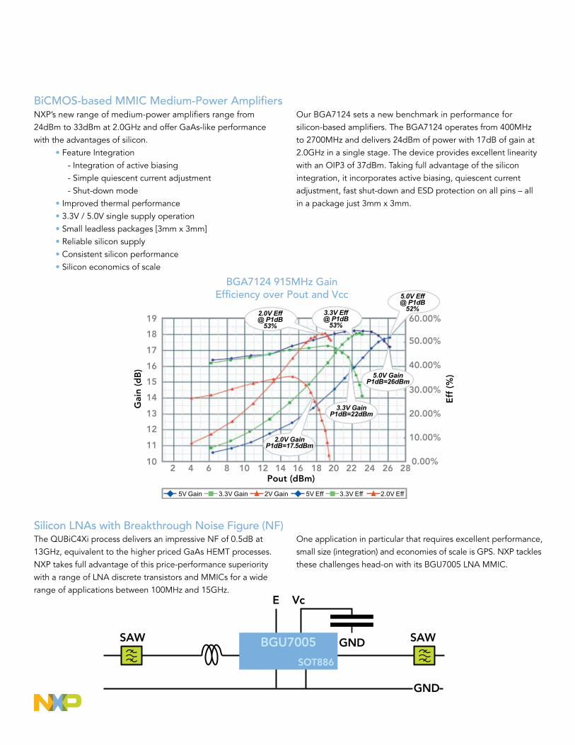
BiCMOS-based MMIC Medium-Power AmplifiersNXP’s new range of medium-power amplifiers range from 24dBm to 33dBm at 2.0GHz and offer GaAs-like performance with the advantages of silicon. • Feature Integration - Integration of active biasing - Simple quiescent current adjustment - Shut-down mode • Improved thermal performance • 3.3V / 5.0V single supply operation • Small leadless packages [3mm x 3mm] • Reliable silicon supply • Consistent silicon performance • Silicon economics of scale
The QUBiC4Xi process delivers an impressive NF of 0.5dB at 13GHz, equivalent to the higher priced GaAs HEMT processes. NXP takes full advantage of this price-performance superiority with a range of LNA discrete transistors and MMICs for a widerange of applications between 100MHz and 15GHz.
Silicon LNAs with Breakthrough Noise Figure (NF)
Our BGA7124 sets a new benchmark in performance for silicon-based amplifiers. The BGA7124 operates from 400MHz to 2700MHz and delivers 24dBm of power with 17dB of gain at 2.0GHz in a single stage. The device provides excellent linearity with an OIP3 of 37dBm. Taking full advantage of the silicon integration, it incorporates active biasing, quiescent current adjustment, fast shut-down and ESD protection on all pins – all in a package just 3mm x 3mm.
One application in particular that requires excellent performance, small size (integration) and economies of scale is GPS. NXP tackles these challenges head-on with its BGU7005 LNA MMIC.
BGA7124 915MHz GainEfficiency over Pout and Vcc
The BGU7005 offers the ultimate in SiGe:C BiCMOS integration, with only 2 external components required to form the LNA function within a GPS receiver. BGU7005 fulfills NF requirements with an outstanding 1.1dB at 1.575GHz while only consuming 5mA of current. In power-down mode the BGU7005 consumes less than 1uA.
With a 6-pin leadless package that requires a minimal amount of board space, 1.45mm x 1.0mm x 0.5mm, the integration level achieved is truly impressive:
• External input match inductor and supply decoupling capacitor • Integrated collector and base RF chokes • Integrated output match • Integrated DC coupling capacitors • Integrated enable pin with low level trigger • ESD protection on all pins
Ruggedness, or the ability to withstand a mismatch condition without failure, is a critical reliability parameter for RF power transistors. NXP has been leading the way in ruggedness since we introduced our first LDMOS transistors nearly a decade ago. Our transistors have proved to be literally indestructible.
NXP has the most advanced LDMOS process worldwide, enabling design of high-efficiency amplifiers with unrivalled ruggedness and the highest gain available. From the most advanced Doherty
designs to new developments in ‘digital switching amplifiers,’ our system architects have developed novel techniques to push amplifier performance to the highest levels.
For tough applications like very high-power broadcast transmitters, our products pass the most stringent ‘hot swap’ tests in the industry, surviving severe high-power VSWR conditions through all angles.
The World’s Most Rugged LDMOS for the Toughest Applications
RF Power Ampliþers
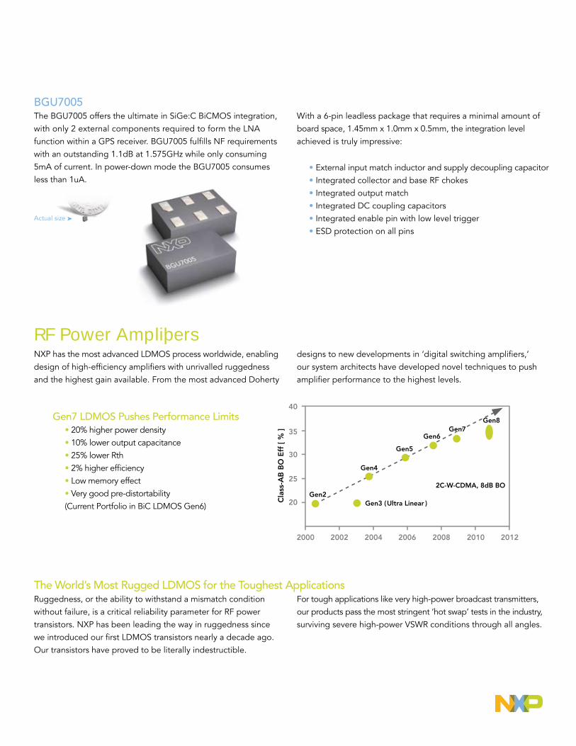
Gen7 LDMOS Pushes Performance Limits • 20% higher power density • 10% lower output capacitance • 25% lower Rth • 2% higher efficiency • Low memory effect • Very good pre-distortability (Current Portfolio in BiC LDMOS Gen6)
BGU7005
kActual size

3-Way Doherty Amplifier Creates a New Standard for Energy Efficiency
NXP GaN - Enabling the Future
Integrated Doherty Transistors Set a New Standard for RF Power Design Simplicity
NXP’s breakthrough 3-way Doherty concept combines the advantages of the Doherty amplifier with our Doherty-optimized Gen7 LDMOS technology to deliver the highest efficiency levels and pre-distortability in a cost-effective package. The Doherty circuit performs at efficiency levels in excess of 47%, at an
Our new gallium-nitride (GaN) technology, the result of a collaborative development effort, enables high-power amplifiers that deliver very high efficiency in next-generation wireless communication systems.
NXP is not only designing next-generation transistors in GaN technology with breakthrough specifications,
NXP has combined the advantages of a Doherty amplifier with the ease of designing-in an ordinary class AB transistor. Resembling an ordinary transistor, these fully integrated Doherty amplifiers deliver the highest efficiency levels and provide significant space and cost savings.
average power output of 48dBm, a gain of 15dB and peak-to-average ratio of 8dB for a multicarrier W-CDMA signal. The current design covers the W-CDMA standard for band 1 operation and is tailored towards high-yield minimum tuning and volume manufacturing.
we’re leading the charge in discovery and innovation in the field of digital transmitter switching power amplifiers based on GaN technology. GaN technology is truly enabling an age of universal transmitters.
Combiner
Splitter
Saturated output power at 50 V: 100WFrequency 2.2GHzMaximum PAE 68%Linear power gain 19dB2C-WCDMA linear efficiency with DPD 40% at -52dBC IM3 at 8dB OPBO
Performance Targets

NXP is leading the way for the next generation of high-speed converters. With NXP’s CGV technology the industry’s first imple-mentation of the JESD204A serial interface – we are transforming high-speed data acquisition, delivering an industry standard-compliant JESD204A product with even greater ease-of-use and performance enhancements.
CGV radically simplifies PCB layout and channel synchronization, setting an entirely new standard for ease-of-use. Fully interoperable with cost-effective FPGAs from Lattice, Altera and Xilinx, NXP’s
CGV-based ADCs and DACs deliver outstanding high input frequency linearity performance. Take the case of a 14 bit dual-channel converter, for example. CGV reduces the 28 wires found in conventional parallel digital interfaces to just 2 differential data lanes. That’s nearly an 80% reduction!
Coupled with our RF portfolio, system-level integration possibilities become a reality. Imagine the potential of being able to utilize data converters, RF/ IF and power amplifiers that are perfectly compatible!
High-Speed Data Converters
DAC1405D750 from NXPDual 16-bit DAC800 MSPS
from Other Vendor
Dynamic Performance

NXP Firsts in RF1963 - Philips diffuses first transistors and diodes on 0.75 inch wafers
1964 - Launches first RF wideband transistor with 1.5GHz max
1970 - Introduces the BFR90, 5GHz wideband transistor
1978 - Introduces the BFQ33, 14GHz wideband transistor
1989 - First to introduce output matching in common emitter basestation transistors
1992 - First to introduce highest-power broadcast bipolar devices
1996 - First to introduce the highest-performance 2GHz LDMOS
1999 - Introduces Bluetooth integrated radio in QUBiC3 BiCMOS process
2000 - NXP follows up with WLAN integrated radio in QUBiC3 BiCMOS process
2001 - First to demonstrate LDMOS-based 250W feedforward power amplifier at European Microwave Conference
2001 - First to fully qualify and introduce LDMOS power amplifier product BLA1011-200 for Pulsed Avionics applications
2001 - Introduces first integrated silicon tuner products in BiCMOS
2003 - First to introduce the ultra-linear LDMOS using Vt distribution at IMS2003
2004 - First to introduce an LDMOS-based 200W Doherty amplifier for UMTS at IMS2004
2004 - Introduces Gen5 LDMOS which becomes the industry’s most advanced process for power amplifiers
2005 - Introduces next level of BiCMOS with QUBiC4+
2006 - First to introduce fully integrated Doherty transistors
2006 - First to introduce ultra-thin leadless packages for breakthrough RF performance
2007 - Launches TFF1004HN, industry’s first fully integrated, silicon-based IC solution for satellite LNB
2007 - First to introduce high-power Novel 3-way Doherty for UMTS/LTE
2007 - NXP shows highest level of integration in BiCMOS with introduction of most advanced WiMAX transceivers
2008 - Introduces the first high-speed data converters based on JESD204A standard
2009 - First to launch 1kW single transistor (BLF578) PA for FM radio (88 to 108MHz)
2009 - First to introduce industry standard radar pallets with LDMOS transistors
2009 - First to introduce state-of-the-art next generation SiGe(C) BiCMOS QUBiC4x technology

Date of release: March 2010Document order number: xxxx xxx xxxxxPrinted in Canada
www.nxp.com
Strong foundation. Advanced technology portfolio. Manufacturing scale. Proven leadership. All good reasons to work with NXP, they are not the only ones. Our approach begins and ends with an unrivaled commitment to your satisfaction. Contact us today to discuss your next project.
We are customerfocused with a passion to win
Experience NXP
©2010 NXP B.V.All rights reserved. Reproduction in whole or in part is prohibited without the prior written consent of the copyright owner. The information presented in this document does not form part of any quotation or contract, is believed to be accurate and reliable and may be changed without notice. No liability will be accepted by the publisher for any consequence of its use. Publication thereof does not convey nor imply any license under patent- or other industrial or intellectual property rights.