Embed Size (px)
Citation preview

Description
The HFBR-0400Z Series of components is designed to provide cost effective, high performance fiber optic com-munication links for information systems and industrial applications with link distances of up to 2.7 kilometers. With the HFBR-24x6Z, the 125 MHz analog receiver, data rates of up to 160 megabaud are attainable.
Transmitters and receivers are directly compatible with popular “industry-standard” connectors: ST®, SMA, SC and FC. They are completely specified with multiple fiber sizes; including 50/125 μm, 62.5/125 μm, 100/140 μm, and 200 μm.
The HFBR-14x4Z high power transmitter and HFBR-24x6Z 125 MHz receiver pair up to provide a duplex solution optimized for 100 Base-SX. 100Base-SX is a Fast Ethernet Standard (100 Mbps) at 850 nm on multimode fiber.
Complete evaluation kits are available for ST product offerings; including transmitter, receiver, connectored cable, and technical literature. In addition, ST connec-tored cables are available for evaluation.
Features
� RoHS Compliant� Meets IEEE 802.3 Ethernet and 802.5 Token Ring Stan-
dards� Meets TIA/EIA-785 100Base-SX standard� Low Cost Transmitters and Receivers� Choice of ST®, SMA, SC or FC Ports� 820 nm Wavelength Technology� Signal Rates up to 160 MBd� Link Distances up to 2.7 km� Compatible with 50/125 μm, 62.5/125 μm, 100/140
μm, and 200 μm HCS® Fiber� Repeatable ST Connections within 0.2 dB Typical� Unique Optical Port Design for Efficient Coupling� Auto-Insertable and Wave Solderable� No Board Mounting Hardware Required� Wide Operating Temperature Range -40 °C to +85 °C� AlGaAs Emitters 100% Burn-In Ensures High Reliability� Conductive Port Option
Applications
� 100Base-SX Fast Ethernet on 850 nm� Media/fiber conversion, switches, routers, hubs and
NICs on 100Base-SX� Local Area Networks� Computer to Peripheral Links� Computer Monitor Links� Digital Cross Connect Links� Central Office Switch/PBX Links� Video Links� Modems and Multiplexers� Suitable for Tempest Systems� Industrial Control Links
ST® is a registered trademark of AT&T.HCS® is a registered trademark of the OFS Corporation.
HFBR-0400Z, HFBR-14xxZ and HFBR-24xxZ SeriesLow Cost, Miniature Fiber Optic Components with ST®, SMA, SC and FC Ports
Data Sheet
2
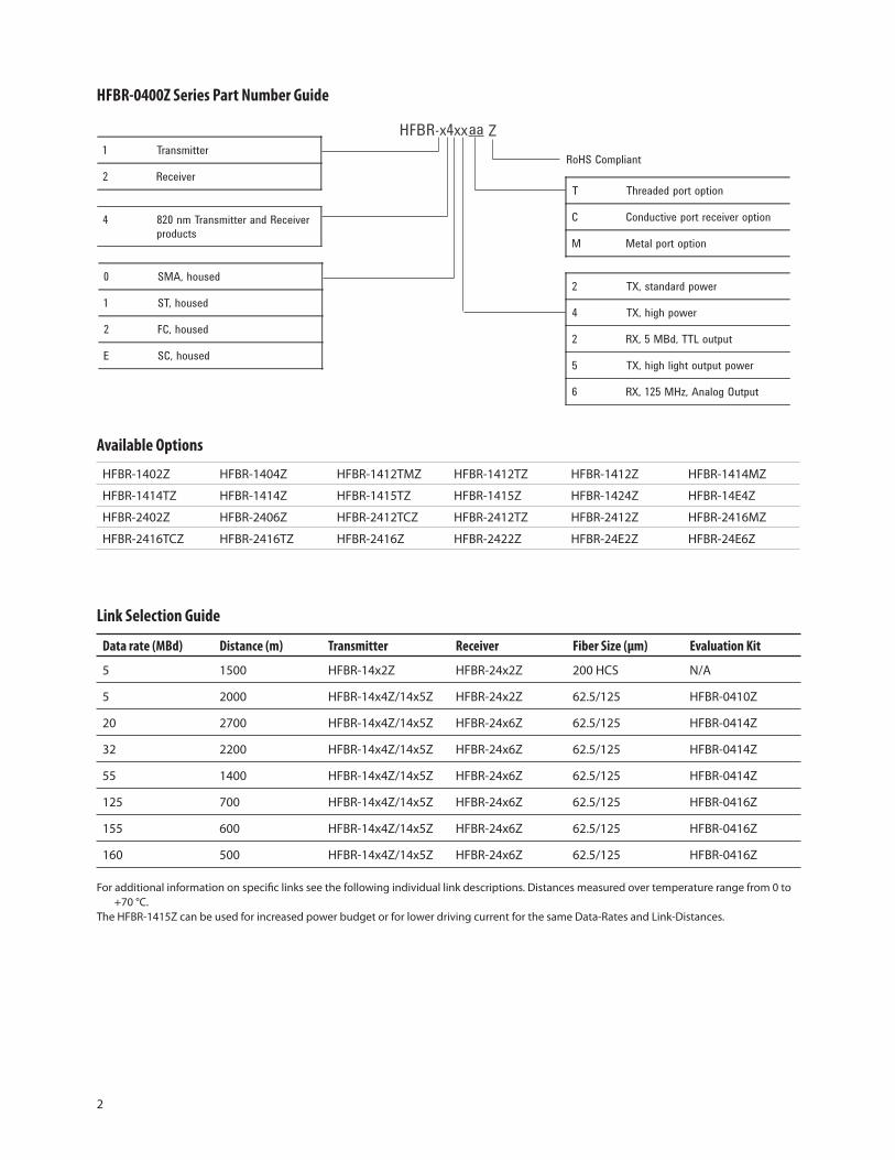
Link Selection Guide
Data rate (MBd) Distance (m) Transmitter Receiver Fiber Size (μm) Evaluation Kit
5 1500 HFBR-14x2Z HFBR-24x2Z 200 HCS N/A
5 2000 HFBR-14x4Z/14x5Z HFBR-24x2Z 62.5/125 HFBR-0410Z
20 2700 HFBR-14x4Z/14x5Z HFBR-24x6Z 62.5/125 HFBR-0414Z
32 2200 HFBR-14x4Z/14x5Z HFBR-24x6Z 62.5/125 HFBR-0414Z
55 1400 HFBR-14x4Z/14x5Z HFBR-24x6Z 62.5/125 HFBR-0414Z
125 700 HFBR-14x4Z/14x5Z HFBR-24x6Z 62.5/125 HFBR-0416Z
155 600 HFBR-14x4Z/14x5Z HFBR-24x6Z 62.5/125 HFBR-0416Z
160 500 HFBR-14x4Z/14x5Z HFBR-24x6Z 62.5/125 HFBR-0416Z
For additional information on specific links see the following individual link descriptions. Distances measured over temperature range from 0 to +70 °C.
The HFBR-1415Z can be used for increased power budget or for lower driving current for the same Data-Rates and Link-Distances.
HFBR-0400Z Series Part Number Guide
HFBR-x4xxaa Z
RoHS Compliant
T Threaded port option
C Conductive port receiver option
M Metal port option
2 TX, standard power
4 TX, high power
2 RX, 5 MBd, TTL output
5 TX, high light output power
6 RX, 125 MHz, Analog Output
1 Transmitter
2 Receiver
0 SMA, housed
1 ST, housed
2 FC, housed
E SC, housed
4 820 nm Transmitter and Receiverproducts
Available Options
HFBR-1402Z HFBR-1404Z HFBR-1412TMZ HFBR-1412TZ HFBR-1412Z HFBR-1414MZ
HFBR-1414TZ HFBR-1414Z HFBR-1415TZ HFBR-1415Z HFBR-1424Z HFBR-14E4Z
HFBR-2402Z HFBR-2406Z HFBR-2412TCZ HFBR-2412TZ HFBR-2412Z HFBR-2416MZ
HFBR-2416TCZ HFBR-2416TZ HFBR-2416Z HFBR-2422Z HFBR-24E2Z HFBR-24E6Z
3
Application Literature
Title Description
HFBR-0400Z Series Reliability Data Transmitter & Receiver Reliability Data
Application Bulletin 78 Low Cost Fiber Optic Links for Digital Applications up to 155 MBd
Application Note 1038 Complete Fiber Solutions for IEEE 802.3 FOIRL, 10Base-FB and 10Base-FL
Application Note 1065 Complete Solutions for IEEE 802.5J Fiberoptic Token Ring
Application Note 1073 HFBR-0219 Test Fixture for 1x9 Fiber Optic Transceivers
Application Note 1086 Optical Fiber Interconnections in Telecommunication Products
Application Note 1121 DC to 32 MBd Fiberoptic Solutions
Application Note 1122 2 to 70 MBd Fiberoptic Solutions
Application Note 1123 20 to 160 MBd Fiberoptic Solutions
Application Note 1137 Generic Printed Circuit Layout Rules
Application Note 1383 Cost Effective Fiber and Media Conversion for 100Base-SX
Applications Support Guide
This section gives the designer information necessary to use the HFBR-0400Z series components to make a func-tional fiber optic transceiver.
Avago Technologies offers a wide selection of evaluation kits for hands-on experience with fiber optic products as well as a wide range of application notes complete with circuit diagrams and board layouts.
Furthermore, Avago Technologies application support group is always ready to assist with any design consid-eration.
4
HFBR-0400Z Series Evaluation Kits
HFBR-0410Z ST Evaluation Kit
Contains the following:
� One HFBR-1412Z transmitter� One HFBR-2412Z five megabaud TTL receiver� Three meters of ST connectored 62.5/125 μm fiber
optic cable with low cost plastic ferrules.� Related literature
HFBR-0414Z ST Evaluation Kit
Includes additional components to interface to the trans-mitter and receiver as well as the PCB to reduce design time. Contains the following:
� One HFBR-1414TZ transmitter� One HFBR-2416TZ receiver� Three meters of ST connectored 62.5/125 μm fiber
optic cable� Printed circuit board� ML-4622 CP Data Quantizer� 74ACTllOOON LED Driver� LT1016CN8 Comparator� 4.7 μH Inductor� Related literature
HFBR-0400Z SMA Evaluation Kit
Contains the following:
� One HFBR-1402Z transmitter� One HFBR-2402Z five megabaud TTL receiver� Two meters of SMA connectored 1000 μm plastic opti-
cal fiber� Related literature
HFBR-0416Z Evaluation Kit
Contains the following:
� One fully assembled 1x9 transceiver board for 155 MBd evaluation including:
- HFBR-1414Z transmitter - HFBR-2416Z receiver - circuitry� Related literature
Ultem® is a registered Trademark of the GE corporation.
Package and Handling Information
Package Information
All HFBR-0400Z Series transmitters and receivers are housed in a low-cost, dual-inline package that is made of high strength, heat resistant, chemically resistant, and UL 94V-O flame retardant ULTEM® plastic (UL File #E121562). The transmitters are easily identified by the light grey color connector port. The receivers are easily identified by the dark grey color connector port. (Black color for conductive port). The package is designed for auto-insertion and wave soldering so it is ideal for high volume production applications.
Handling and Design Information
Each part comes with a protective port cap or plug cov-ering the optics. These caps/plugs will vary by port style. When soldering, it is advisable to leave the protective cap on the unit to keep the optics clean. Good system performance requires clean port optics and cable ferrules to avoid obstructing the optical path.
Clean compressed air often is sufficient to remove parti-cles of dirt; methanol on a cotton swab also works well.
Recommended Chemicals for Cleaning/Degreasing
HFBR-0400Z Products
Alcohols: methyl, isopropyl, isobutyl. Aliphatics: hexane, heptane, Other: soap solution, naph-tha.
Do not use partially halogenated hydrocarbons such as 1,1.1 trichloroethane, ketones such as MEK, acetone, chloroform, ethyl acetate, methylene dichloride, phenol, methylene chloride, or N-methylpyrolldone. Also, Avago Technologies does not recommend the use of cleaners that use halogenated hydrocarbons because of their potential environmental harm.
5
6.35(0.25)
2.54(0.10)
3.81(0.15)
6.4(0.25) DIA.
12.7(0.50)
12.7(0.50)
22.2(0.87)
5.1(0.20)
10.2(0.40)
3.6(0.14)
1.27(0.05)
2.54(0.10)
PINS 1,4,5,80.51 X 0.38
(0.020 X 0.015)
PINS 2,3,6,70.46
(0.018)DIA. 81
3
5
24
67
PIN NO. 1INDICATOR
1/4 - 36 UNS 2A THREAD
Rx/
TxC
OU
NTR
Y O
FO
RIG
INA
YYW
WH
FBR
-X40
XZ
8.2(0.32)
Rx/
TxC
OU
NTR
Y O
FO
RIG
INA
YYW
WH
FBR
-X41
XZ
6.35(0.25)
12.7(0.50)
27.2(1.07)
5.1(0.20)
10.2(0.40)
3.6(0.14)
1.27(0.05)
2.54(0.10)
PINS 1,4,5,80.51 X 0.38
(0.020 X 0.015)
PINS 2,3,6,70.46
(0.018)DIA. 81
3
5
24
67
PIN NO. 1INDICATOR
2.54(0.10)
3.81(0.15)
DIA.
12.7(0.50)
7.0(0.28)
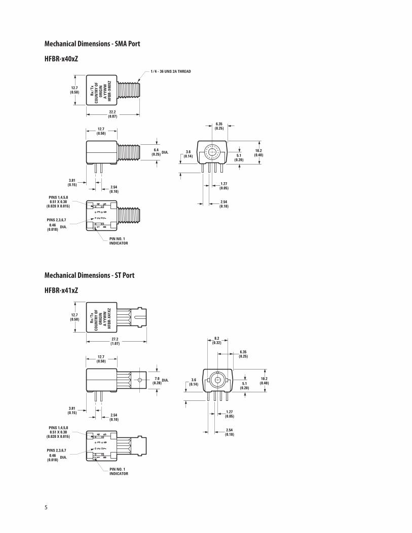
Mechanical Dimensions - SMA Port
HFBR-x40xZ
Mechanical Dimensions - ST Port
HFBR-x41xZ
6
5.1(0.20)
3/8 - 32 UNEF - 2A
Rx/
TxC
OU
NTR
Y O
FO
RIG
INA
YYW
WH
FBR
-X41
XTZ
8.4(0.33)
6.35(0.25)
12.7(0.50)
27.2(1.07)
5.1(0.20)
10.2(0.40)
3.6(0.14)
1.27(0.05)
2.54(0.10)
PINS 1,4,5,80.51 X 0.38
(0.020 X 0.015)
PINS 2,3,6,70.46
(0.018)DIA. 81
3
5
24
67
PIN NO. 1INDICATOR
2.54(0.10)
3.81(0.15)
DIA.
12.7(0.50)
7.1(0.28)
DIA.
7.6(0.30)
M8 x 0.75 6GTHREAD (METRIC)
Rx/
TxC
OU
NTR
Y O
FO
RIG
INA
YYW
WH
FBR
-X42
XZ
2.5(0.10)
3.81(0.15)
7.9(0.31)
12.7(0.50)
12.7(0.50)
5.1(0.20)
10.2(0.40)
3.6(0.14)
813
5
24
67
PIN NO. 1INDICATOR
19.6(0.77)
2.5(0.10)
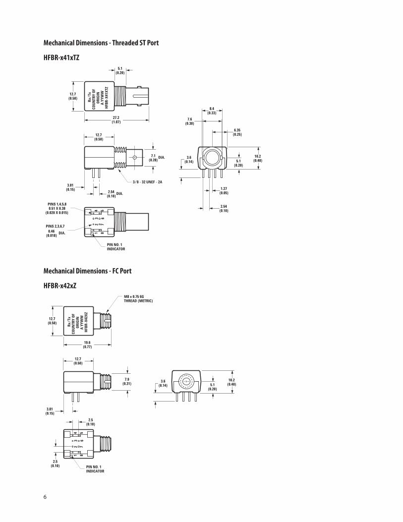
Mechanical Dimensions - Threaded ST Port
HFBR-x41xTZ
Mechanical Dimensions - FC Port
HFBR-x42xZ
7
28.65(1.128)
15.95(0.628)
10.0(0.394)
12.7(0.500)
Rx/
TxC
OU
NTR
Y O
FO
RIG
INA
YYW
WH
FBR
-X4E
XZ
12.7(0.50)
2.54(0.10)
3.81(0.15)
6.35(0.25)
5.1(0.200)
10.38(0.409)3.60
(0.140)
1.27(0.050)
2.54(0.100)
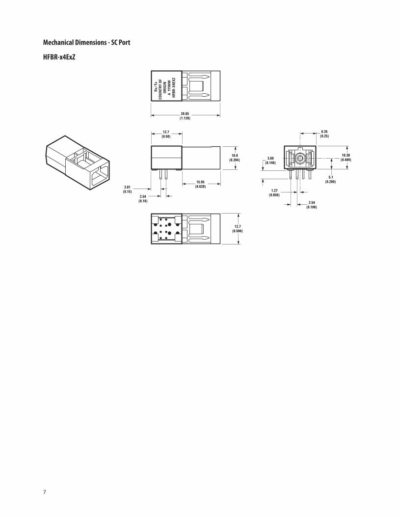
Mechanical Dimensions - SC Port
HFBR-x4ExZ
8
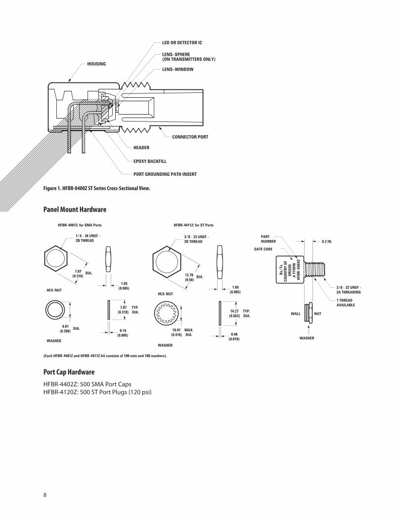
(Each HFBR-4401Z and HFBR-4411Z kit consists of 100 nuts and 100 washers).
7.87(0.310)
7.87(0.310)
DIA.
1/4 - 36 UNEF -2B THREAD
1.65(0.065)
TYP.DIA.
6.61(0.260)
DIA.
HEX-NUT
WASHER
0.14(0.005)
14.27(0.563)
12.70(0.50)
DIA.
3/8 - 32 UNEF -2B THREAD
1.65(0.065)
TYP.DIA.
10.41(0.410)
MAX.DIA.
HEX-NUT
WASHER
0.46(0.018)
3/8 - 32 UNEF - 2A THREADING
0.2 IN.
WALL
WASHER
NUT
1 THREAD AVAILABLE
DATE CODE
PARTNUMBER
Rx/
TxC
OU
NTR
Y O
FO
RIG
INA
YYW
WH
FBR
-X40
XZ
HFBR-4401Z: for SMA Ports HFBR-4411Z: for ST Ports
Port Cap Hardware
HFBR-4402Z: 500 SMA Port Caps HFBR-4120Z: 500 ST Port Plugs (120 psi)
Figure 1. HFBR-0400Z ST Series Cross-Sectional View.
Panel Mount Hardware
HOUSING
CONNECTOR PORT
HEADER
EPOXY BACKFILL
PORT GROUNDING PATH INSERT
LED OR DETECTOR IC
LENS–SPHERE(ON TRANSMITTERS ONLY)
LENS–WINDOW
9
Options
In addition to the various port styles available for the HFBR- 0400Z series products, there are also several extra options that can be ordered. To order an option, simply place the corresponding option number at the end of the part number. See page 2 for available options.
Option T (Threaded Port Option)
� Allows ST style port components to be panel mount-ed.
� Compatible with all current makes of ST® multimode connectors
� Mechanical dimensions are compliant with MIL-STD- 83522/13
� Maximum wall thickness when using nuts and wash-ers from the HFBR-4411Z hardware kit is 2.8 mm (0.11 inch)
� Available on all ST ports
Option C (Conductive Port Receiver Option)
� Designed to withstand electrostatic discharge (ESD) of 25 kV to the port
� Significantly reduces effect of electromagnetic inter-ference (EMI) on receiver sensitivity
� Allows designer to separate the signal and conductive port grounds
� Recommended for use in noisy environments� Available on SMA and threaded ST port style receivers
only
Option M (Metal Port Option)
� Nickel plated aluminum connector receptacle� Designed to withstand electrostatic discharge (ESD) of
15 kV to the port� Significantly reduces effect of electromagnetic inter-
ference (EMI) on receiver sensitivity� Allows designer to separate the signal and metal port
grounds� Recommended for use in very noisy environments� Available on SMA, ST, and threaded ST ports
10
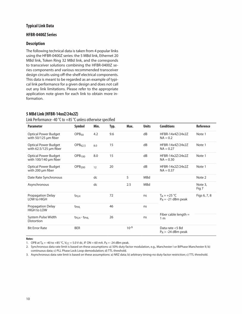
Typical Link Data
HFBR-0400Z Series
Description
The following technical data is taken from 4 popular links using the HFBR-0400Z series: the 5 MBd link, Ethernet 20 MBd link, Token Ring 32 MBd link, and the corresponds to transceiver solutions combining the HFBR-0400Z se-ries components and various recommended transceiver design circuits using off-the-shelf electrical components. This data is meant to be regarded as an example of typi-cal link performance for a given design and does not call out any link limitations. Please refer to the appropriate application note given for each link to obtain more in-formation.
5 MBd Link (HFBR-14xxZ/24x2Z)
Link Performance -40 °C to +85 °C unless otherwise specified
Parameter Symbol Min. Typ. Max. Units Conditions Reference
Optical Power Budgetwith 50/125 μm fiber
OPB50 4.2 9.6 dB HFBR-14x4Z/24x2ZNA = 0.2
Note 1
Optical Power Budgetwith 62.5/125 μm fiber
OPB62.5 8.0 15 dB HFBR-14x4Z/24x2ZNA = 0.27
Note 1
Optical Power Budgetwith 100/140 μm fiber
OPB100 8.0 15 dB HFBR-14x2Z/24x2ZNA = 0.30
Note 1
Optical Power Budgetwith 200 μm fiber
OPB200 12 20 dB HFBR-14x2Z/24x2ZNA = 0.37
Note 1
Date Rate Synchronous dc 5 MBd Note 2
Asynchronous dc 2.5 MBd Note 3,Fig 7
Propagation DelayLOW to HIGH
tPLH 72 ns TA = +25 °CPR = -21 dBm peak
Fiber cable length = 1 m
Figs 6, 7, 8
Propagation DelayHIGH to LOW
tPHL 46 ns
System Pulse WidthDistortion
tPLH - tPHL 26 ns
Bit Error Rate BER 10-9 Data rate <5 BdPR > -24 dBm peak
Notes:
1. OPB at TA = -40 to +85 °C, VCC = 5.0 V dc, IF ON = 60 mA. PR = -24 dBm peak.2. Synchronous data rate limit is based on these assumptions: a) 50% duty factor modulation, e.g., Manchester I or BiPhase Manchester II; b)
continuous data; c) PLL Phase Lock Loop demodulation; d) TTL threshold.3. Asynchronous data rate limit is based on these assumptions: a) NRZ data; b) arbitrary timing-no duty factor restriction; c) TTL threshold.
11
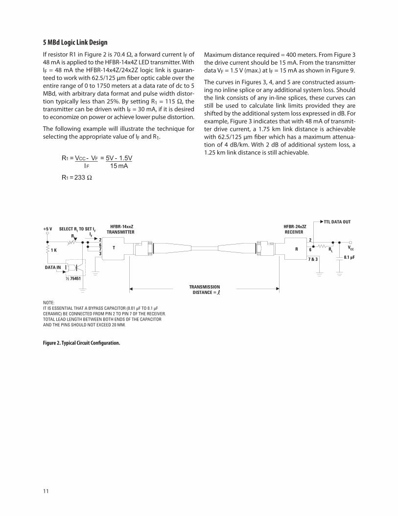
5 MBd Logic Link Design
If resistor R1 in Figure 2 is 70.4 �, a forward current IF of 48 mA is applied to the HFBR-14x4Z LED transmitter. With IF = 48 mA the HFBR-14x4Z/24x2Z logic link is guaran-teed to work with 62.5/125 μm fiber optic cable over the entire range of 0 to 1750 meters at a data rate of dc to 5 MBd, with arbitrary data format and pulse width distor-tion typically less than 25%. By setting R1 = 115 �, the transmitter can be driven with IF = 30 mA, if it is desired to economize on power or achieve lower pulse distortion.
The following example will illustrate the technique for selecting the appropriate value of IF and R1.
Figure 2. Typical Circuit Configuration.
+5 V SELECT R1 TO SET IF
R1IF
1 K
DATA IN
½ 75451
2673
T
HFBR-14xxZTRANSMITTER
TRANSMISSIONDISTANCE =
HFBR-24x2ZRECEIVER
R
TTL DATA OUT
2
6
7 & 3
RLVCC
0.1 μF
NOTE:IT IS ESSENTIAL THAT A BYPASS CAPACITOR (0.01 μF TO 0.1 μFCERAMIC) BE CONNECTED FROM PIN 2 TO PIN 7 OF THE RECEIVER.TOTAL LEAD LENGTH BETWEEN BOTH ENDS OF THE CAPACITORAND THE PINS SHOULD NOT EXCEED 20 MM.
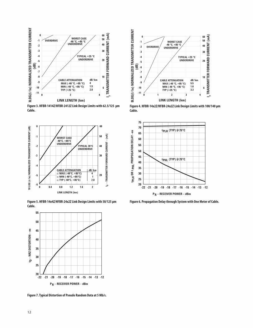
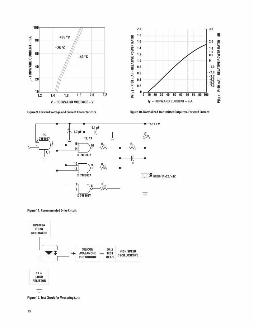
Maximum distance required = 400 meters. From Figure 3 the drive current should be 15 mA. From the transmitter data VF = 1.5 V (max.) at IF = 15 mA as shown in Figure 9.
The curves in Figures 3, 4, and 5 are constructed assum-ing no inline splice or any additional system loss. Should the link consists of any in-line splices, these curves can still be used to calculate link limits provided they are shifted by the additional system loss expressed in dB. For example, Figure 3 indicates that with 48 mA of transmit-ter drive current, a 1.75 km link distance is achievable with 62.5/125 μm fiber which has a maximum attenua-tion of 4 dB/km. With 2 dB of additional system loss, a 1.25 km link distance is still achievable.
=
-=-=
233 ΩR
mA15I1.5V5VVVR
1
F
FCC1
12
0LO
G(I
/Io)
NO
RM
ALI
ZED
TR
AN
SMIT
TER
CU
RR
ENT
(dB
)0
-1
-2
-3
-4
-5
-6
-7
-8
-9
-10
-11
I F TR
AN
SMIT
TER
FO
RW
AR
D C
UR
REN
T (m
A)
60
50
40
30
20
10
6
420
LINK LENGTH (km)
CABLE ATTENUATION MAX (-40 °C, +85 °C) MIN (-40 °C, +85 °C) TYP (+25 °C)
dB/km41.52.8
OVERDRIVEWORST CASE
-40 °C, +85 °CUNDERDRIVE
TYPICAL +25 °CUNDERDRIVE
0LO
G(I
/Io)
NO
RM
ALI
ZED
TR
AN
SMIT
TER
CU
RR
ENT
(dB
)
0
-1
-2
-3
-4
-5
-6
-7
-8
-9
-10
-11
I F TR
AN
SMIT
TER
FO
RW
AR
D C
UR
REN
T (m
A)
60
50
40
30
20
10
6
420
LINK LENGTH (km)
CABLE ATTENUATION MAX (-40 °C, +85 °C) MIN (-40 °C, +85 °C) TYP (+25 °C)
dB/km5.51.03.3
OVERDRIVE
WORST CASE-40 °C, +85 °C
UNDERDRIVE
TYPICAL +25 °CUNDERDRIVE
1 3
75
-22 -21 -20 -19 -18 -17 -16 -15 -14 -13 -12
PR – RECEIVER POWER – dBm
tPL
H O
R t
PHL
PRO
POG
ATI
ON
DEL
AY
–ns
70
65
60
55
50
45
40
35
30
25
20
tPLH (TYP) @ 25°C
tPHL (TYP) @ 25°C
55
-22 -21 -20 -19 -18 -17 -16 -15 -14 -13 -12
PR – RECEIVER POWER – dBm
t D –
NR
Z D
ISTO
RTI
ON
– n
s
50
45
40
35
30
25
20
Figure 5. HFBR-14x4Z/HFBR-24x2Z Link Design Limits with 50/125 μm
Cable.
Figure 6. Propagation Delay through System with One Meter of Cable.
Figure 4. HFBR-14x2Z/HFBR-24x2Z Link Design Limits with 100/140 μm
Cable.
Figure 3. HFBR-1414Z/HFBR-2412Z Link Design Limits with 62.5/125 μm
Cable.
Figure 7. Typical Distortion of Pseudo Random Data at 5 Mb/s.
0
-1
-2
-3
-4
-5
-60 0.4 0.8 1.2 1.6 2
10 L
OG
(t/
to)
NO
RM
ALI
ZED
TR
AN
SMIT
TER
CU
RR
ENT
(dB
)
LINK LENGTH (km)
I F –
TR
AN
SMIT
TER
FO
RW
AR
D C
UR
REN
T –
(mA
)
60
50
40
30
20
WORST CASE-40°C, +85°CUNDERDRIVE
CABLE ATTENUATION dB/km α MAX (-40°C, +85°C) 4α MIN (-40°C, +85°C) 1α TYP (-40°C, +85°C) 2.8
TYPICAL 26°CUNDERDRIVE
13
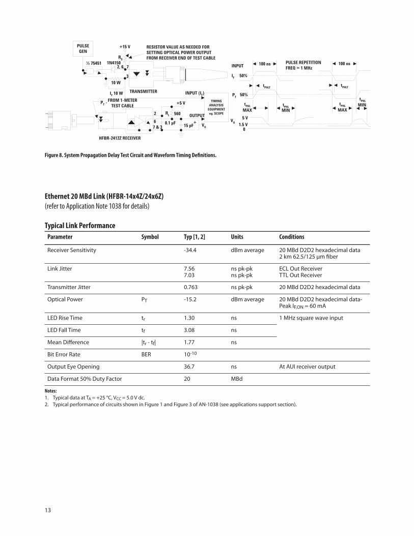
Figure 8. System Propagation Delay Test Circuit and Waveform Timing Definitions.
IF 10 W
PULSEGEN
½ 75451 1N4150
10 W
+15 V
RS
2, 6, 7
RESISTOR VALUE AS NEEDED FORSETTING OPTICAL POWER OUTPUTFROM RECEIVER END OF TEST CABLE
3
TRANSMITTER
PT -FROM 1-METER
TEST CABLE
INPUT (IF)
2
67 & 3
+VO15 pF
RL
+5 V
560
0.1 μF
OUTPUT
TIMINGANALYSIS
EQUIPMENTeg. SCOPE
HFBR-2412Z RECEIVER
INPUT
IF
PT
VO
50%
50%
tPHL
MAX
5 V
1.5 V0
tPHLT
100 ns
tPHLMIN
PULSE REPETITIONFREQ = 1 MHz
100 ns
tPHLT
tPHL
MAX
tPHL
MIN
Ethernet 20 MBd Link (HFBR-14x4Z/24x6Z)
(refer to Application Note 1038 for details)
Typical Link Performance
Parameter Symbol Typ [1, 2] Units Conditions
Receiver Sensitivity -34.4 dBm average 20 MBd D2D2 hexadecimal data2 km 62.5/125 μm fiber
Link Jitter 7.567.03
ns pk-pkns pk-pk
ECL Out ReceiverTTL Out Receiver
Transmitter Jitter 0.763 ns pk-pk 20 MBd D2D2 hexadecimal data
Optical Power PT -15.2 dBm average 20 MBd D2D2 hexadecimal data-Peak IF,ON = 60 mA
LED Rise Time tr 1.30 ns 1 MHz square wave input
LED Fall Time tf 3.08 ns
Mean Difference |tr - tf| 1.77 ns
Bit Error Rate BER 10-10
Output Eye Opening 36.7 ns At AUI receiver output
Data Format 50% Duty Factor 20 MBd
Notes:
1. Typical data at TA = +25 °C, VCC = 5.0 V dc.2. Typical performance of circuits shown in Figure 1 and Figure 3 of AN-1038 (see applications support section).
14
Token Ring 32 MBd Link (HFBR-14x4Z/24x6Z)
(refer to Application Note 1065 for details)
Typical Link Performance
Parameter Symbol Typ [1, 2] Units Conditions
Receiver Sensitivity -34.1 dBm average 32 MBd D2D2 hexadecimal data2 km 62.5/125 μm fiber
Link Jitter 6.915.52
ns pk-pkns pk-pk
ECL Out ReceiverTTL Out Receiver
Transmitter Jitter 0.823 ns pk-pk 32 MBd D2D2 hexadecimal data
Optical Power Logic Level “0” PT ON -12.2 dBm peak Transmitter TTL in IF ON = 60 mA,IF OFF = 1 mA
Optical Power Logic Level “1” PT OFF -82.2
LED Rise Time tr 1.3 ns 1 MHz square wave input
LED Fall Time tf 3.08 ns
Mean Difference |tr - tf| 1.77 ns
Bit Error Rate BER 10-10
Data Format 50% Duty Factor 32 MBd
Notes:
1. Typical data at TA = +25 °C, VCC = 5.0 V dc.2. Typical performance of circuits shown in Figure 1 and Figure 3 of AN-1065 (see applications support section)
155 MBd Link (HFBR-14x4Z/24x6Z)
(refer to Application Bulletin 78 for details)
Typical Link Performance
Parameter Symbol Min Typ [1, 2] Max Units Conditions Ref
Optical Power Budget with 50/125 μm fiber
OPB50 7.9 13.9 dB NA = 0.2 Note 2
Optical Power Budgetwith 62.5/125 μm fiber
OPB62 11.7 17.7 dB NA = 0.27
Optical Power Budgetwith 100/140 μm fiber
OPB100 11.7 17.7 dB NA = 0.30
Optical Power Budgetwith 200 μm HCS fiber
OPB200 16.0 22.0 dB NA = 0.35
Data Format 20% to 80% Duty Factor
1 175 MBd
System Pulse WidthDistortion
|tPLH - tPHL| 1 ns PR = -7 dBm peak1 m 62.5/125 μm fiber
Bit Error Rate BER 10-9 Data rate < 100 MBaudPR > -31 dBm peak
Note 2
Notes:
1. Typical data at TA = +25 °C, VCC = 5.0 V dc, PECL serial interface.2. Typical OPB was determined at a probability of error (BER) of 10-9. Lower probabilities of error can be achieved with short fibers that have
less optical loss.
15
HFBR-14x2Z/14x4Z Low-Cost High-Speed Transmitters
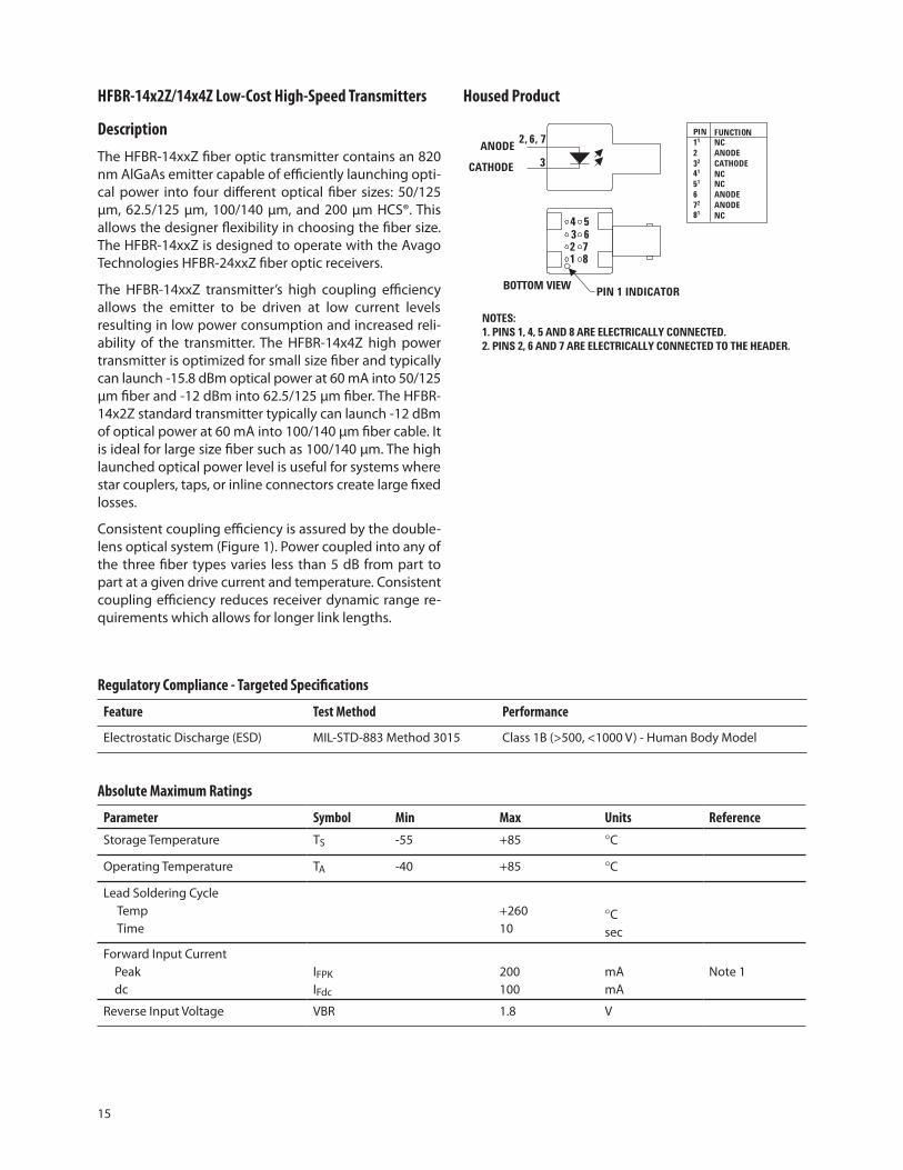
Description
The HFBR-14xxZ fiber optic transmitter contains an 820 nm AlGaAs emitter capable of efficiently launching opti-cal power into four different optical fiber sizes: 50/125 μm, 62.5/125 μm, 100/140 μm, and 200 μm HCS®. This allows the designer flexibility in choosing the fiber size. The HFBR-14xxZ is designed to operate with the Avago Technologies HFBR-24xxZ fiber optic receivers.
The HFBR-14xxZ transmitter’s high coupling efficiency allows the emitter to be driven at low current levels resulting in low power consumption and increased reli-ability of the transmitter. The HFBR-14x4Z high power transmitter is optimized for small size fiber and typically can launch -15.8 dBm optical power at 60 mA into 50/125 μm fiber and -12 dBm into 62.5/125 μm fiber. The HFBR-14x2Z standard transmitter typically can launch -12 dBm of optical power at 60 mA into 100/140 μm fiber cable. It is ideal for large size fiber such as 100/140 μm. The high launched optical power level is useful for systems where star couplers, taps, or inline connectors create large fixed losses.
Consistent coupling efficiency is assured by the double-lens optical system (Figure 1). Power coupled into any of the three fiber types varies less than 5 dB from part to part at a given drive current and temperature. Consistent coupling efficiency reduces receiver dynamic range re-quirements which allows for longer link lengths.
Housed Product
Regulatory Compliance - Targeted Specifications
Feature Test Method Performance
Electrostatic Discharge (ESD) MIL-STD-883 Method 3015 Class 1B (>500, <1000 V) - Human Body Model
Absolute Maximum Ratings
Parameter Symbol Min Max Units Reference
Storage Temperature TS -55 +85 �C
Operating Temperature TA -40 +85 �C
Lead Soldering Cycle Temp Time
+26010
�Csec
Forward Input Current Peak dc
IFPKIFdc
200100
mAmA
Note 1
Reverse Input Voltage VBR 1.8 V
ANODE
CATHODE
2, 6, 7
3
PIN11
232
41
51
672
81
FUNCTIONNCANODECATHODENCNCANODEANODENC
4321
5678
PIN 1 INDICATORBOTTOM VIEW
NOTES:1. PINS 1, 4, 5 AND 8 ARE ELECTRICALLY CONNECTED.2. PINS 2, 6 AND 7 ARE ELECTRICALLY CONNECTED TO THE HEADER.
16
Electrical/Optical Specifications -40 °C to +85 °C unless otherwise specified.
Parameter Symbol Min Typ2 Max Units Conditions Reference
Forward Voltage VF 1.48 1.701.84
2.09 V IF = 60 mA dcIF = 100 mA dc
Figure 9
Forward Voltage TemperatureCoefficient
�VF/�T -0.22-0.18
mV/�C IF = 60 mA dcIF = 100 mA dc
Figure 9
Reverse Input Voltage VBR 1.8 3.8 V IF = 100 μA dc
Peak Emission Wavelength lP 792 820 865 nm
Diode Capacitance CT 55 pF V = 0, f = 1 MHz
Optical Power Temperature Coefficient
�PT/�T -0.006-0.010
dB/�C I = 60 mA dcI = 100 mA dc
Thermal Resistance �JA 260 �C/W Notes 3, 8
14x2Z Numerical Aperture NA 0.49
14x4Z Numerical Aperture NA 0.31
14x2Z Optical Port Diameter D 290 μm Note 4
14x4Z Optical Port Diameter D 150 μm Note 4
HFBR-14x2Z Output Power Measured Out of 1 Meter of Cable
Parameter Symbol Min Typ Max Units Conditions Reference
50/125 �m Fiber Cable PT50 -21.8 -18.8 -16.8 dBm peak TA = +25 °C,IF = 60mA dc
Notes 5, 6, 9
-22.8 -15.8
-20.3 -16.8 -14.4 TA = +25 °C,IF = 100mA dc-21.9 -13.8
62.5/125 �m Fiber Cable PT62 -19.0 -16.0 -14.0 dBm peak TA = +25 °C,IF = 60mA dc-20.0 -13.0
-17.5 -14.0 -11.6 TA = +25 °C,IF = 100mA dc-19.1 -11.0
100/140 �m Fiber Cable PT100 -15.0 -12.0 -10 dBm peak TA = +25 °C,IF = 60mA dc-16.0 -9.0
-13.5 -10.0 -7.6 TA = +25 °C,IF = 100mA dc-15.1 -7.0
200 �m HCS Fiber Cable PT200 -10.0 -7.0 -5.0 dBm peak TA = +25 °C,IF = 60mA dc-11.0 -4.0
-8.5 -5.0 -2.6 TA = +25 °C,IF = 100mA dc-10.1 -2.0
CAUTION: The small junction sizes inherent to the design of these components increase the components’ susceptibility to damage from electrostatic discharge (ESD). It is advised that normal static precautions be taken in handling and assembly of these components to prevent damage and/or degradation which may be induced by ESD.
17
HFBR-14x4Z Output Power Measured out of 1 Meter of Cable
Parameter Symbol Min Typ2 Max Units Conditions Reference
50/125 μm Fiber CableNA = 0.2
PT50 -18.8-19.8
-15.8 -13.8-12.8
dBm peak
TA = +25 °C,IF = 60mA dc
Notes 5, 6, 9
-17.3-18.9
-13.8 -11.4-10.8
TA = +25 °C,IF = 100 mA dc
62.5/125 μm Fiber CableNA = 0.275
PT62 -15.0-16.0
-12.0 -10.0-9.0
dBm peak
TA = +25 °C,IF = 60mA dc
-13.5-15.1
-10.0 -7.6-7.0
TA = +25 °C,IF = 100 mA dc
100/140 μm Fiber CableNA = 0.3
PT100 -11.5-12.5
-8.5 -6.5-5.5
dBm peak
TA = +25 °C,IF = 60mA dc
-10.0-11.6
-6.5 -4.1-3.5
TA = +25 °C,IF = 100 mA dc
200 μm HCS Fiber CableNA = 0.37
PT200 -7.5-8.5
-4.5 -2.5-1.5
dBm peak
TA = +25 °C,IF = 60mA dc
-6.0-7.6
-2.5 -0.10.5
TA = +25 °C,IF = 100 mA dc
HFBR-14x5Z Output Power Measured out of 1 Meter of Cable
Parameter Symbol Min Typ Max Units Conditions
200μm Fiber CableNA = 0.37
PT200 -6.0 -3.6 0.0 dBm peak TA = +25°C, IF = 60mA
-7.0 1.0 dBm peak TA = -40°C to 85°C, IF = 60mA
62.5/125μm Fiber CableNA = 0.275
PT62 -12.0 -10.5 -8.0 dBm peak TA = +25°C, IF = 60mA
-13.0 -7.0 dBm peak TA = -40°C to 85°C, IF = 60mA
50/125μm Fiber CableNA = 0.2
PT50 -16.5 -14.3 -11.5 dBm peak TA = +25°C, IF = 60mA
-17.5 -10.5 dBm peak TA = -40°C to 85°C, IF = 60mA
14x2Z/14x4Z/14x5Z Dynamic Characteristics
Parameter Symbol Min Typ2 Max Units Conditions Reference
Rise Time, Fall Time(10% to 90%)
tr, tf 4.0 6.5 nsecNo pre-bias
IF = 60 mAFigure 12
Note 7
Rise Time, Fall Time(10% to 90%)
tr, tf 3.0 nsec IF = 10 to 100 mA Note 7, Figure 11
Pulse Width Distortion PWD 0.5 nsec Figure 11
Notes:
1. For IFPK > 100 mA, the time duration should not exceed 2 ns.2. Typical data at TA = +25 °C.3. Thermal resistance is measured with the transmitter coupled to a connector assembly and mounted on a printed circuit board.4. D is measured at the plane of the fiber face and defines a diameter where the optical power density is within 10 dB of the maximum.5. PT is measured with a large area detector at the end of 1 meter of mode stripped cable, with an ST® precision ceramic ferrule (MILSTD-
83522/13) for HFBR-1412Z/1414Z, and with an SMA 905 precision ceramic ferrule for HFBR-1402Z/1404Z.6. When changing mW to dBm, the optical power is referenced to 1 mW (1000 mW). Optical Power P (dBm) = 10 log P (mW)/1000 mW.7. Pre-bias is recommended if signal rate >10 MBd, see recommended drive circuit in Figure 11.8. Pins 2, 6 and 7 are welded to the anode header connection to minimize the thermal resistance from junction to ambient. To further reduce
the thermal resistance, the anode trace should be made as large as is consistent with good RF circuit design.9. Fiber NA is measured at the end of 2 meters of mode stripped fiber, using the far-field pattern. NA is defined as the sine of the half angle,
determined at 5% of the peak intensity point. When using other manufacturer’s fiber cable, results will vary due to differing NA values and specification methods.
18
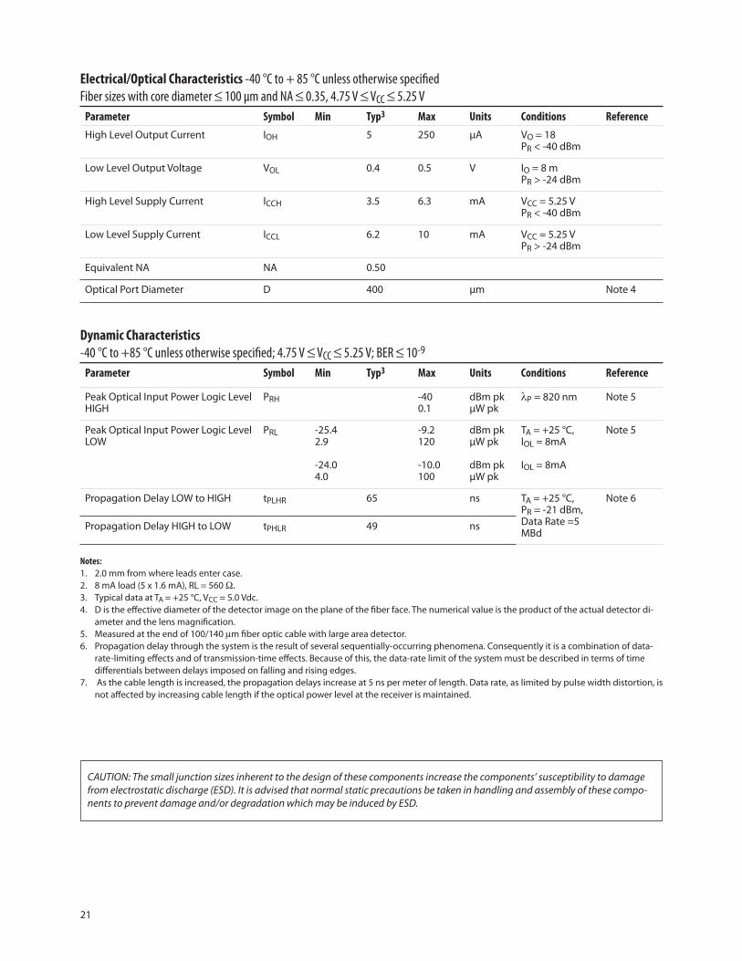
Recommended Drive Circuits
The circuit used to supply current to the LED transmitter can significantly influence the optical switching charac-teristics of the LED. The optical rise/fall times and propa-gation delays can be improved by using the appropriate circuit techniques. The LED drive circuit shown in Figure 11 uses frequency compensation to reduce the typical rise/fall times of the LED and a small pre-bias voltage to minimize propagation delay differences that cause pulse-width distortion. The circuit will typically produce rise/fall times of 3 ns, and a total jitter including pulse-width dis-
tortion of less than 1 ns. This circuit is recommended for applications requiring low edge jitter or high-speed data transmission at signal rates of up to 155 MBd. Component values for this circuit can be calculated for different LED drive currents using the equations shown below. For additional details about LED drive circuits, the reader is encouraged to read Avago Technologies Application Bul-letin 78 and Application Note 1038.
All HFBR-14XXZ LED transmitters are classified as IEC 825-1 Accessible Emission Limit (AEL) Class 1 based upon the current proposed draft scheduled to go in to effect on January 1, 1997. AEL Class 1 LED devices are considered eye safe. Contact your Avago Technologies sales representative for more information.
CAUTION: The small junction sizes inherent to the design of these components increase the components’ susceptibility to damage from electrostatic discharge (ESD). It is advised that normal static precautions be taken in handling and assembly of these components to prevent damage and/or degradation which may be induced by ESD.
. V)1.84( 9 Figure from obtained be can V:100mAI for Example
)(Rps 2000 C(pF)
)3(R R R R
1R)( R
3.97R
21R
(A) I1.6V)V3.97(V)V(VR
FON F
X1
EQ2X3X2
X1EQ2
YX1
ON F
FCCFCCY
X4
==
Ω=
===
-=Ω
)=
--+-
pF 16911.8
ps 2000C
32.4 (10.8) 3 R R R
10.8 1 - 11.8 R
11.83.9793.5
21R
93.50.100
6.193.16R
0.1001.6)1.843.97(51.84)(5R
X4X3X2
EQ2
X1
Y
Y
=Ω
=
Ω====
Ω==
Ω==
Ω=+=
--+-=
()(
19
Figure 11. Recommended Drive Circuit.
P(I F
) –
P(60
mA
) –
REL
ATI
VE P
OW
ER R
ATI
O
0
2.0
0.8
0
IF – FORWARD CURRENT – mA
20 40 80
1.6
0.4
1.2
60 100
1.8
1.4
1.0
0.6
0.2
10 30 50 70 90
P(I F
) –
P(60
mA
) –
REL
ATI
VE P
OW
ER R
ATI
O –
dB
-7.0-5.0-4.0-3.0-2.0
-1.0
0
0.81.01.4
2.0
3.0
HP8082APULSE
GENERATOR
SILICONAVALANCHEPHOTODIODE
50 ΩTESTHEAD
HIGH SPEEDOSCILLOSCOPE
50 ΩLOAD
RESISTOR
100
80
60
40
20
101.2 1.4 1.6 1.8 2.0 2.2
VI - FORWARD VOLTAGE - V
I F - F
OR
WA
RD
CU
RREN
T -
mA +85 °C
+25 °C
-40 °C
HFBR-14x2Z/x4Z
+5 V
Ry
RX1
C
¼ 74F3037
7
8 5 RX4
¼ 74F3037
RX3
RX2
¼74F3037
1
23
4, 5
+4.7 μF
15
14
¼ 74F3037
16
12, 13
0.1 μF
10
119
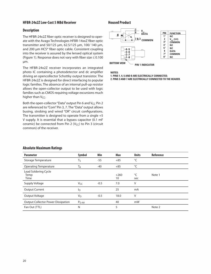
Figure 9. Forward Voltage and Current Characteristics. Figure 10. Normalized Transmitter Output vs. Forward Current.
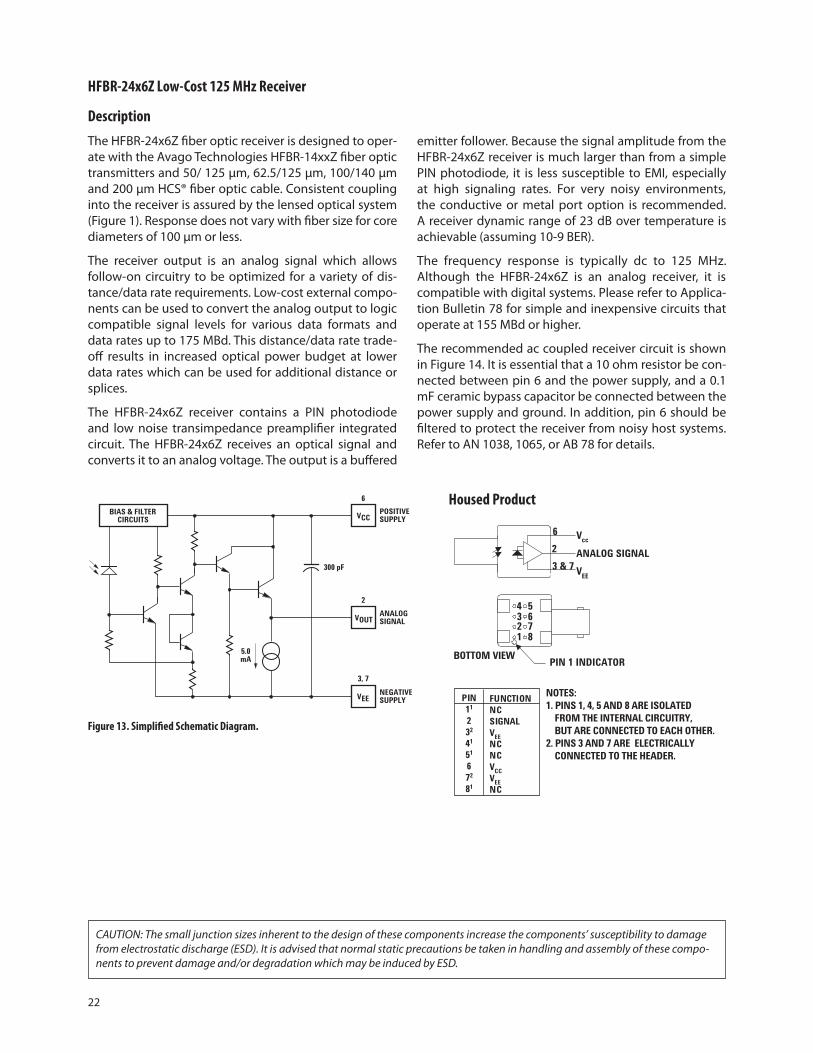
Figure 12. Test Circuit for Measuring tr, tf.
20
HFBR-24x2Z Low-Cost 5 MBd Receiver
Description
The HFBR-24x2Z fiber optic receiver is designed to oper-ate with the Avago Technologies HFBR-14xxZ fiber optic transmitter and 50/125 μm, 62.5/125 μm, 100/ 140 μm, and 200 μm HCS® fiber optic cable. Consistent coupling into the receiver is assured by the lensed optical system (Figure 1). Response does not vary with fiber size � 0.100 μm.
The HFBR-24x2Z receiver incorporates an integrated photo IC containing a photodetector and dc amplifier driving an opencollector Schottky output transistor. The HFBR-24x2Z is designed for direct interfacing to popular logic families. The absence of an internal pull-up resistor allows the open-collector output to be used with logic families such as CMOS requiring voltage excursions much higher than VCC.
Both the open-collector “Data” output Pin 6 and VCC Pin 2 are referenced to “Com” Pin 3, 7. The “Data” output allows busing, strobing and wired “OR” circuit configurations. The transmitter is designed to operate from a single +5 V supply. It is essential that a bypass capacitor (0.1 mF ceramic) be connected from Pin 2 (VCC) to Pin 3 (circuit common) of the receiver.
Absolute Maximum Ratings
Parameter Symbol Min Max Units Reference
Storage Temperature TS -55 +85 °C
Operating Temperature TA -40 +85 °C
Lead Soldering Cycle Temp Time
+26010
°Csec
Note 1
Supply Voltage VCC -0.5 7.0 V
Output Current IO 25 mA
Output Voltage VO -0.5 18.0 V
Output Collector Power Dissipation PO AV 40 mW
Fan Out (TTL) N 5 Note 2
Housed Product
VccDATA
COMMON
26
7 & 3
4 5678
321
PIN11
232
41
51
672
81
FUNCTIONNCV
CC (5 V)
COMMONNCNCDATACOMMONNC
PIN 1 INDICATORBOTTOM VIEW
NOTES:1. PINS 1, 4, 5 AND 8 ARE ELECTRICALLY CONNECTED.2. PINS 3 AND 7 ARE ELECTRICALLY CONNECTED TO THE HEADER.
21
CAUTION: The small junction sizes inherent to the design of these components increase the components’ susceptibility to damage from electrostatic discharge (ESD). It is advised that normal static precautions be taken in handling and assembly of these compo-nents to prevent damage and/or degradation which may be induced by ESD.
Electrical/Optical Characteristics -40 °C to + 85 °C unless otherwise specified
Fiber sizes with core diameter � 100 μm and NA � 0.35, 4.75 V � VCC � 5.25 V
Parameter Symbol Min Typ3 Max Units Conditions Reference
High Level Output Current IOH 5 250 μA VO = 18PR < -40 dBm
Low Level Output Voltage VOL 0.4 0.5 V IO = 8 mPR > -24 dBm
High Level Supply Current ICCH 3.5 6.3 mA VCC = 5.25 VPR < -40 dBm
Low Level Supply Current ICCL 6.2 10 mA VCC = 5.25 VPR > -24 dBm
Equivalent NA NA 0.50
Optical Port Diameter D 400 μm Note 4
Dynamic Characteristics
-40 °C to +85 °C unless otherwise specified; 4.75 V � VCC � 5.25 V; BER � 10-9
Parameter Symbol Min Typ3 Max Units Conditions Reference
Peak Optical Input Power Logic Level HIGH
PRH -400.1
dBm pkμW pk
P = 820 nm Note 5
Peak Optical Input Power Logic Level LOW
PRL -25.42.9
-24.04.0
-9.2120
-10.0100
dBm pk μW pk
dBm pk μW pk
TA = +25 °C, IOL = 8mA
IOL = 8mA
Note 5
Propagation Delay LOW to HIGH tPLHR 65 ns TA = +25 °C,PR = -21 dBm,Data Rate =5 MBd
Note 6
Propagation Delay HIGH to LOW tPHLR 49 ns
Notes:
1. 2.0 mm from where leads enter case.2. 8 mA load (5 x 1.6 mA), RL = 560 �.3. Typical data at TA = +25 °C, VCC = 5.0 Vdc.4. D is the effective diameter of the detector image on the plane of the fiber face. The numerical value is the product of the actual detector di-
ameter and the lens magnification.5. Measured at the end of 100/140 �m fiber optic cable with large area detector.6. Propagation delay through the system is the result of several sequentially-occurring phenomena. Consequently it is a combination of data-
rate-limiting effects and of transmission-time effects. Because of this, the data-rate limit of the system must be described in terms of time differentials between delays imposed on falling and rising edges.
7. As the cable length is increased, the propagation delays increase at 5 ns per meter of length. Data rate, as limited by pulse width distortion, is not affected by increasing cable length if the optical power level at the receiver is maintained.
22
HFBR-24x6Z Low-Cost 125 MHz Receiver
Description
The HFBR-24x6Z fiber optic receiver is designed to oper-ate with the Avago Technologies HFBR-14xxZ fiber optic transmitters and 50/ 125 μm, 62.5/125 μm, 100/140 μm and 200 μm HCS® fiber optic cable. Consistent coupling into the receiver is assured by the lensed optical system (Figure 1). Response does not vary with fiber size for core diameters of 100 μm or less.
The receiver output is an analog signal which allows follow-on circuitry to be optimized for a variety of dis-tance/data rate requirements. Low-cost external compo-nents can be used to convert the analog output to logic compatible signal levels for various data formats and data rates up to 175 MBd. This distance/data rate trade-off results in increased optical power budget at lower data rates which can be used for additional distance or splices.
The HFBR-24x6Z receiver contains a PIN photodiode and low noise transimpedance preamplifier integrated circuit. The HFBR-24x6Z receives an optical signal and converts it to an analog voltage. The output is a buffered
Housed Product
Figure 13. Simplified Schematic Diagram.
CAUTION: The small junction sizes inherent to the design of these components increase the components’ susceptibility to damage from electrostatic discharge (ESD). It is advised that normal static precautions be taken in handling and assembly of these compo-nents to prevent damage and/or degradation which may be induced by ESD.
emitter follower. Because the signal amplitude from the HFBR-24x6Z receiver is much larger than from a simple PIN photodiode, it is less susceptible to EMI, especially at high signaling rates. For very noisy environments, the conductive or metal port option is recommended. A receiver dynamic range of 23 dB over temperature is achievable (assuming 10-9 BER).
The frequency response is typically dc to 125 MHz. Although the HFBR-24x6Z is an analog receiver, it is compatible with digital systems. Please refer to Applica-tion Bulletin 78 for simple and inexpensive circuits that operate at 155 MBd or higher.
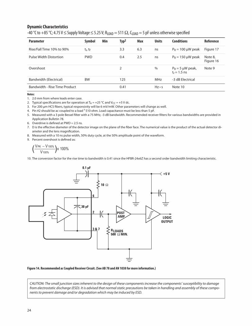
The recommended ac coupled receiver circuit is shown in Figure 14. It is essential that a 10 ohm resistor be con-nected between pin 6 and the power supply, and a 0.1 mF ceramic bypass capacitor be connected between the power supply and ground. In addition, pin 6 should be filtered to protect the receiver from noisy host systems. Refer to AN 1038, 1065, or AB 78 for details.
BIAS & FILTERCIRCUITS VCC
VOUT
VEE
6
2
3, 7
POSITIVESUPPLY
ANALOGSIGNAL
NEGATIVESUPPLY
5.0mA
300 pF
Vcc
ANALOG SIGNAL
VEE
2
6
3 & 7
4 5678
321
PIN11
232
41
51
672
81
FUNCTIONNCSIGNALVEENCNCVCCVEENC
PIN 1 INDICATORBOTTOM VIEW
NOTES:1. PINS 1, 4, 5 AND 8 ARE ISOLATED FROM THE INTERNAL CIRCUITRY, BUT ARE CONNECTED TO EACH OTHER.2. PINS 3 AND 7 ARE ELECTRICALLY CONNECTED TO THE HEADER.
23
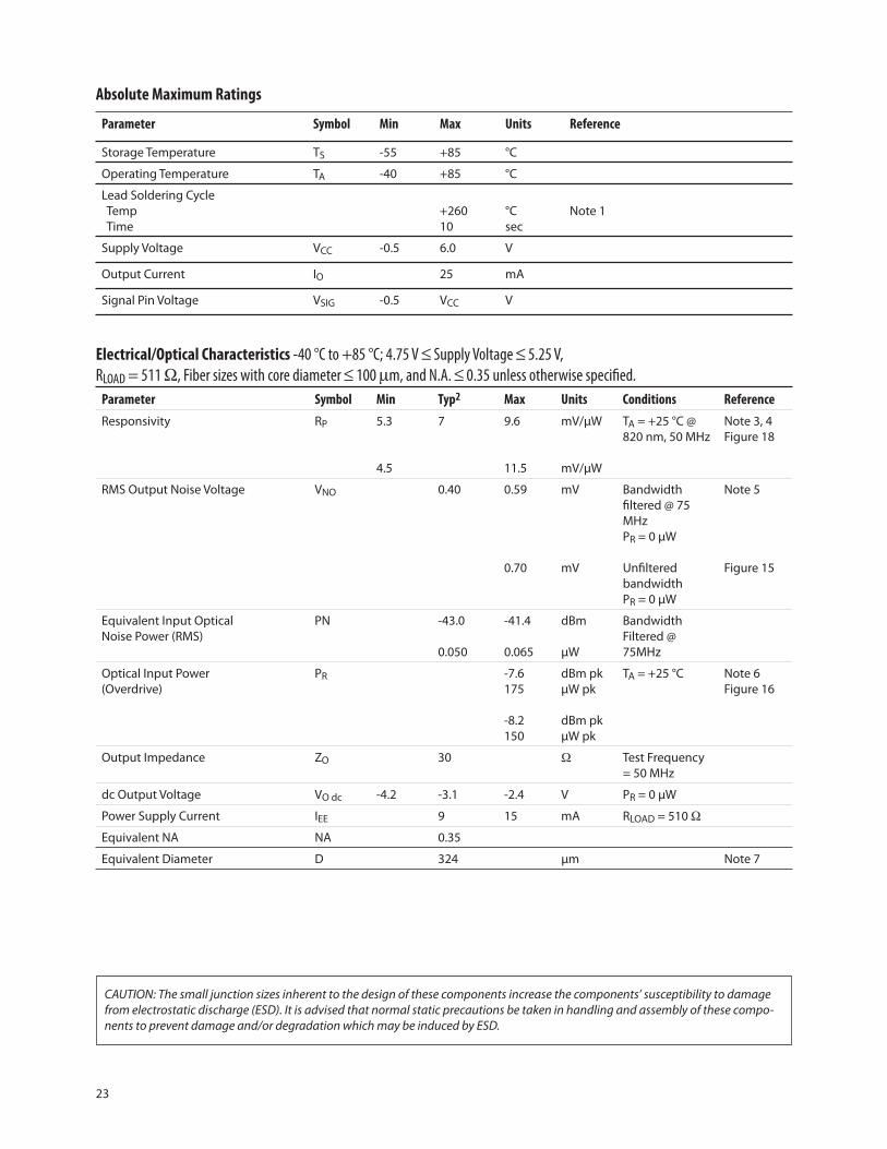
Absolute Maximum Ratings
Parameter Symbol Min Max Units Reference
Storage Temperature TS -55 +85 °C
Operating Temperature TA -40 +85 °C
Lead Soldering Cycle Temp Time
+26010
°Csec
Note 1
Supply Voltage VCC -0.5 6.0 V
Output Current IO 25 mA
Signal Pin Voltage VSIG -0.5 VCC V
Electrical/Optical Characteristics -40 °C to +85 °C; 4.75 V � Supply Voltage � 5.25 V,
RLOAD = 511 �, Fiber sizes with core diameter � 100 �m, and N.A. � 0.35 unless otherwise specified.
Parameter Symbol Min Typ2 Max Units Conditions Reference
Responsivity RP 5.3
4.5
7 9.6
11.5
mV/μW
mV/μW
TA = +25 °C @ 820 nm, 50 MHz
Note 3, 4Figure 18
RMS Output Noise Voltage VNO 0.40 0.59
0.70
mV
mV
Bandwidth filtered @ 75 MHzPR = 0 μW
UnfilteredbandwidthPR = 0 μW
Note 5
Figure 15
Equivalent Input OpticalNoise Power (RMS)
PN -43.0
0.050
-41.4
0.065
dBm
μW
BandwidthFiltered @ 75MHz
Optical Input Power(Overdrive)
PR -7.6175
-8.2150
dBm pkμW pk
dBm pk μW pk
TA = +25 °C Note 6Figure 16
Output Impedance ZO 30 � Test Frequency = 50 MHz
dc Output Voltage VO dc -4.2 -3.1 -2.4 V PR = 0 μW
Power Supply Current IEE 9 15 mA RLOAD = 510 �
Equivalent NA NA 0.35
Equivalent Diameter D 324 μm Note 7
CAUTION: The small junction sizes inherent to the design of these components increase the components’ susceptibility to damage from electrostatic discharge (ESD). It is advised that normal static precautions be taken in handling and assembly of these compo-nents to prevent damage and/or degradation which may be induced by ESD.
24
Dynamic Characteristics
-40 °C to +85 °C; 4.75 V � Supply Voltage � 5.25 V; RLOAD = 511 �, CLOAD = 5 pF unless otherwise specified
Parameter Symbol Min Typ2 Max Units Conditions Reference
Rise/Fall Time 10% to 90% tr, tf 3.3 6.3 ns PR = 100 μW peak Figure 17
Pulse Width Distortion PWD 0.4 2.5 ns PR = 150 μW peak Note 8, Figure 16
Overshoot 2 % PR = 5 μW peak, tr = 1.5 ns
Note 9
Bandwidth (Electrical) BW 125 MHz -3 dB Electrical
Bandwidth - Rise Time Product 0.41 Hz • s Note 10
Notes:
1. 2.0 mm from where leads enter case.2. Typical specifications are for operation at TA = +25 °C and VCC = +5 V dc.3. For 200 μm HCS fibers, typical responsivity will be 6 mV/mW. Other parameters will change as well.4. Pin #2 should be ac coupled to a load ³ 510 ohm. Load capacitance must be less than 5 pF.5. Measured with a 3 pole Bessel filter with a 75 MHz, -3 dB bandwidth. Recommended receiver filters for various bandwidths are provided in
Application Bulletin 78.6. Overdrive is defined at PWD = 2.5 ns.7. D is the effective diameter of the detector image on the plane of the fiber face. The numerical value is the product of the actual detector di-
ameter and the lens magnification.8. Measured with a 10 ns pulse width, 50% duty cycle, at the 50% amplitude point of the waveform.9. Percent overshoot is defined as:
10. The conversion factor for the rise time to bandwidth is 0.41 since the HFBR-24x6Z has a second order bandwidth limiting characteristic.
CAUTION: The small junction sizes inherent to the design of these components increase the components’ susceptibility to damage from electrostatic discharge (ESD). It is advised that normal static precautions be taken in handling and assembly of these compo-nents to prevent damage and/or degradation which may be induced by ESD.
Figure 14. Recommended ac Coupled Receiver Circuit. (See AB 78 and AN 1038 for more information.)
100%x V
VV100%
100%PK( − )
0.1 μF
LOGICOUTPUT
+5 V
10 Ω
30 pF
RLOADS500 Ω MIN.
6
2
3 & 7
POSTAMP
For product information and a complete list of distributors, please go to our web site: www.avagotech.com
Avago, Avago Technologies, and the A logo are trademarks of Avago Technologies in the United States and other countries.
Data subject to change. Copyright © 2005-2011 Avago Technologies. All rights reserved. Obsoletes AV01-0264EN
AV02-0176EN - March 23, 2011
150
0 50 100 150 200 250
FREQUENCY – MHZ
125
100
75
50
25
0300
SPEC
TRA
L N
OIS
E D
ENSI
TY –
nV/
HZ
3.0
0 20 30 40 50 70
PR – INPUT OPTICAL POWER – μW
2.5
2.0
1.5
1.0
0.5
080
PWD
– P
ULS
E W
IDTH
DIS
TOR
TIO
N –
ns
10 60
6.0
-60 -40 -20 0 20 40
TEMPERATURE – °C
5.0
4.0
3.0
2.0
1.060
tr,
t f –
RES
PON
SE T
IME
– ns
80 100
tf
tr
1.25
400 480 560 640 720 800
λ – WAVELENGTH – nm
1.00
0.75
0880
NO
RM
ALI
ZED
RES
PON
SE
0.50
0.25
960 1040
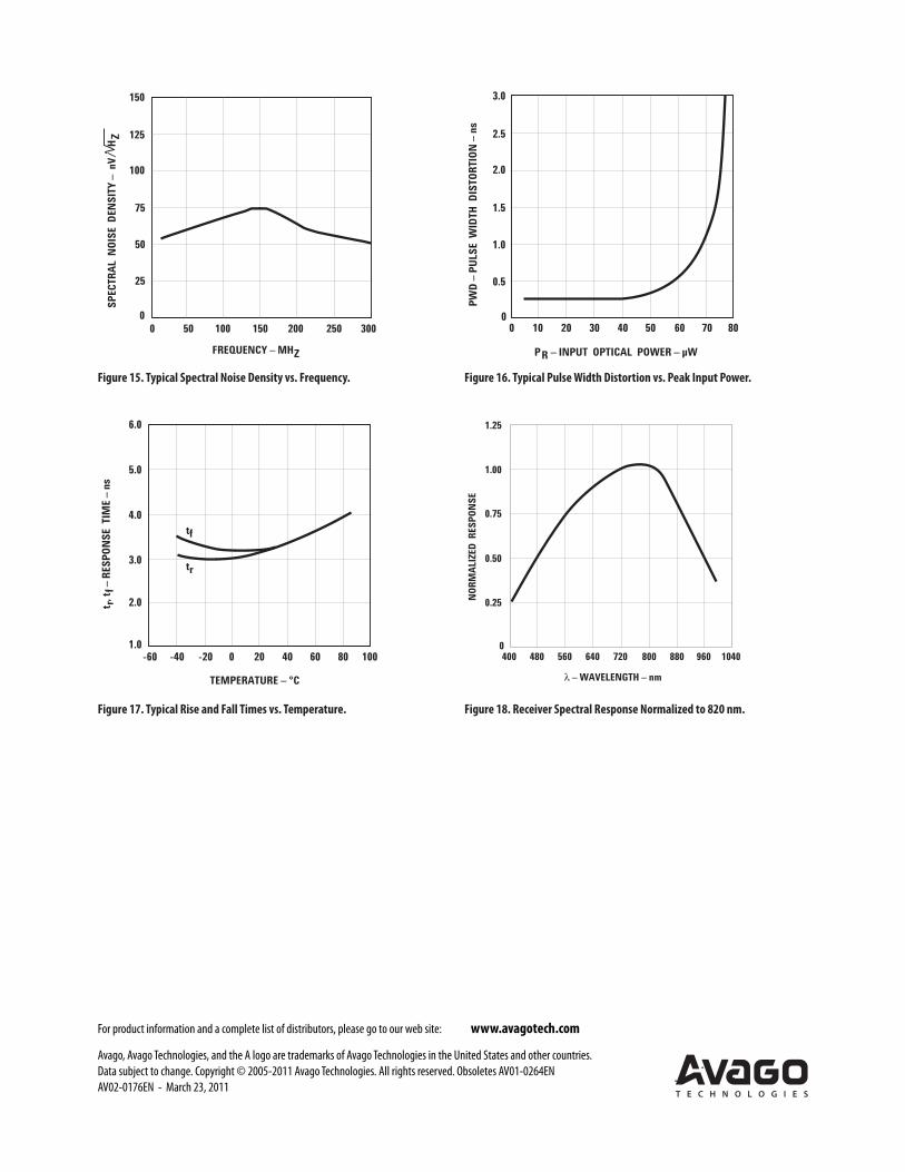
Figure 15. Typical Spectral Noise Density vs. Frequency. Figure 16. Typical Pulse Width Distortion vs. Peak Input Power.
Figure 17. Typical Rise and Fall Times vs. Temperature. Figure 18. Receiver Spectral Response Normalized to 820 nm.