Embed Size (px)
Citation preview

Features RoHS Compliant Low cost per Gb/s High package density per Gb/s 3.3 volt power supply for low power consumption 850 nm VCSEL array source 12 independent channels per module Separate transmitter and receiver modules 2.7 Gbd data rate per channel Standard MTP® (MPO) ribbon fiber connector
interface Pluggable package 50/125 micron multimode fiber operation:
Distance up to 300 m with500 MHz.km fiber at 2.5 GbdDistance up to 600 m with2000 MHz.km fiber at 2.5 Gbd
Data I/O is CML compatible Control I/O is LVTTL compatible Manufactured in an ISO 9002 certified facility
Applications Datacom switch and router backplane connections Telecom switch and router backplane connections InfiniBand connections
Ordering InformationThe HFBR-772BZ and HFBR-782BZ products areavailable for production orders through the AvagoComponent Field Sales office.
HFBR-772BZ No EMI Nose Shield
HFBR-782BZ No EMI Nose Shield
HFBR-772BEZ With Extended EMI Nose Shield
HFBR-782BEZ With Extended EMI Nose Shield
HFBR-772BHZ No Heatsink, No EMI Nose Shield
HFBR-782BHZ No Heatsink, No Nose Shield
HFBR-772BEHZ With Extended EMI Nose Shield, NoHeatsink
HFBR-782BEHZ With Extended EMI Nose Shield, NoHeatsink
DescriptionThe HFBR-772BZ transmitter and HFBR-782BZreceiver are high performance fiber optic modulesfor parallel optical data communicationapplications. These 12-channel devices, operatingup to 2.7 Gbd per channel, provide a costeffective solution for short-reach applicationsrequiring up to 32 Gb/s aggregate bandwidth.These modules are designed to operate onmultimode fiber systems at a nominal wavelengthof 850 nm. They incorporate high performance,highly reliable, short wavelength optical devicescoupled with proven circuit technology to providelong life and consistent service.
The HFBR-772BZ transmitter module incorporatesa 12- channel VCSEL (Vertical Cavity SurfaceEmitting Laser) array together with a custom 12-channel laser driver integrated circuit providingIEC-60825 and CDRH Class 1M laser eye safety.
The HFBR-782BZ receiver module contains a 12-channel PIN photodiode array coupled with acustom preamplifier / post amplifier integratedcircuit.
Operating from a single +3.3 V power supply,both modules provide LVTTL or LVCMOS controlinterfaces and Current Mode Logic (CML)compatible data interfaces to simplify externalcircuitry.
The transmitter and receiver devices are housedin MTP®/MPO receptacled packages. Electricalconnections to the devices are achieved by meansof a pluggable 10 x 10 connector array.
HFBR-772BZ/BEZ/BHZ/BEHZ andHFBR-782BZ/BEZ/BHZ/BEHZPluggable Parallel Fiber Optic Modules, Transmitter and Receiver
Datasheet
2
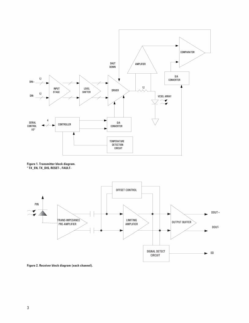
Design Summary:Design for low-cost, high-volume manufacturingAvago’s parallel optics solution combines twelve2.7 Gbd channels into discrete transmitter andreceiver modules providing a maximumaggregate data rate of 32 Gb/s. Moreover, thesemodules employ a heat sink for thermalmanagement when used on high-density cards,have excellent EMI performance, and interfacewith the industry standard MTP®/MPOconnector systems. They provide the most cost-effective high- density (Gbd per inch) solutionsfor high-data capacity applications. See Figure1 for the transmitter and Figure 2 for thereceiver block diagrams.
The HFBR-772BZ transmitter and the HFBR-782BZ receiver modules provide very closelyspaced, high-speed parallel data channels.Within these modules there will be some levelof cross talk between channels. The cross talkwithin the modules will be exhibited asadditional data jitter or sensitivity reductioncompared to single-channel performance. AvagoTechnologies’ jitter and sensitivity specificationsinclude cross talk penalties and thus representreal, achievable module performance.
Functional Description, Transmitter SectionThe transmitter section, Figure 1, uses a 12-channel 850 nm VCSEL array as the opticalsource and a diffractive optical lens array tolaunch the beam of light into the fiber. Thepackage and connector system are designed toallow repeatable coupling into standard 12-fiberribbon cable. In addition, this module has beendesigned to be compliant with IEC 60825 Class1 eye safety requirements.
The optical output is controlled by a custom IC,which provides proper laser drive parametersand monitors drive current to ensure eyesafety. An EEPROM and state machine areprogrammed to provide both ac and dc currentdrive to the laser to ensure correct modulation,eye diagram and extinction ratio overvariations of temperature and power supplyvoltages.
Functional Description, Receiver SectionThe receiver section, Figure 2, contains a 12-channel AlGaAs/ GaAs photodetector array,transimpedance preamplifier, filter, gain stagesto amplify and buffer the signal, and aquantizer to shape the signal.
The Signal Detect function is designed to sensethe proper optical output signal on each of the12 channels. If loss of signal is detected on anindividual channel, that channel output issquelched.
PackagingThe flexible electronic subassembly wasdesigned to allow high-volume assembly andtest of the VCSEL, PIN photo diode andsupporting electronics prior to final assembly.
Regulatory ComplianceThe overall equipment design into which theparallel optics module is mounted willdetermine the certification level. The moduleperformance is offered as a figure of merit toassist the designer in considering their use inthe equipment design.
Organization RecognitionSee the Regulatory Compliance Table for alisting of the standards, standards associationsand testing laboratories applicable to thisproduct.
Electrostatic Discharge (ESD)There are two design cases in which immunityto ESD damage is important.
The first case is during handling of the moduleprior to mounting it on the circuit board. It isimportant to use normal ESD handlingprecautions for ESD sensitive devices. Theseprecautions include using grounded wriststraps, work benches, and floor mats in ESDcontrolled areas.
The second case to consider is static dischargesto the exterior of the equipment chassiscontaining the module parts. To the extent thatthe MTP® (MPO) connector receptacle isexposed to the outside of the equipment chassisit may be subject to system level ESD testcriteria that the equipment is intended to meet.
See the Regulatory Compliance Table for furtherdetails.
3
Figure 1. Transmitter block diagram.* TX_EN, TX_DIS, RESET-, FAULT-
Figure 2. Receiver block diagram (each channel).
SIGNAL DETECTCIRCUIT
TRANS-IMPEDANCEPRE-AMPLIFIER
LIMITINGAMPLIFIER
OUTPUT BUFFER
OFFSET CONTROL
PIN
DOUT+
DOUT-
SD
D/ACONVERTER
INPUTSTAGE
LEVELSHIFTER
DRIVER
AMPLIFIER
COMPARATOR
TEMPERATUREDETECTION
CIRCUIT
D/ACONVERTER
CONTROLLER
12
VCSEL ARRAY
DIN+
DIN-
SERIALCONTROL
I/O*
4
SHUTDOWN
12
12
4
Electromagnetic Interference (EMI)Many equipment designs using these high-data-rate modules will be required to meet therequirements of the FCC in the United States,CENELEC in Europe and VCCI in Japan. Thesemodules, with their shielded design, perform tothe levels detailed in the Regulatory ComplianceTable. The performance detailed in theRegulatory Compliance Table is intended toassist the equipment designer in themanagement of the overall equipment EMIperformance. However, system margins aredependent on the customer board and chassisdesign.
ImmunityEquipment using these modules will be subjectto radio frequency electromagnetic fields insome environments. These modules have goodimmunity due to their shielded designs. See theRegulatory Compliance Table for further detail.
Eye SafetyThese 850 nm VCSEL-based modules provideeye safety by design. The HFBR-772BZ hasbeen registered with CDRH and certified byTUV as a Class 1M device under Amendment 2of IEC 60825-1. See the Regulatory ComplianceTable for further detail. If Class 1M exposure ispossible, a safety-warning label should beplaced on the product stating the following:
LASER RADIATIONDO NOT VIEW DIRECTLY WITHOPTICAL INSTRUMENTSCLASS 1M LASER PRODUCT
Connector CleaningThe optical connector used is the MTP® (MPO).The optical ports have recessed optics that arevisible through the nose of the ports. Theprovided port plug should be installed any timea fiber cable is not connected. The port plugensures the optics remain clean and nocleaning should be necessary. In the event theoptics become contaminated, forced nitrogen orclean dry air at less than 20 psi is therecommended cleaning agent. The optical portfeatures, including guide pins, preclude use ofany solid instrument. Liquids are not adviseddue to potential damage.
Process PlugEach parallel optics module is supplied with aninserted process plug for protection of theoptical ports within the MTP® (MPO) connectorreceptacle.
Handling PrecautionsThe HFBR-772BZ and HFBR-782BZ can bedamaged by current surges and overvoltageconditions. Power supply transient precautionsshould be taken. Application of wavesoldering, reflow soldering and/or aqueous washprocesses with the parallel optic device onboard is not recommended as damage mayoccur.
Normal handling precautions for electrostaticsensitive devices should be taken (see ESDsection).
The HFBR-772BZ is a Class 1M laser product.DO NOT VIEW RADIATION DIRECTLY WITHOPTICAL INSTRUMENTS.
5
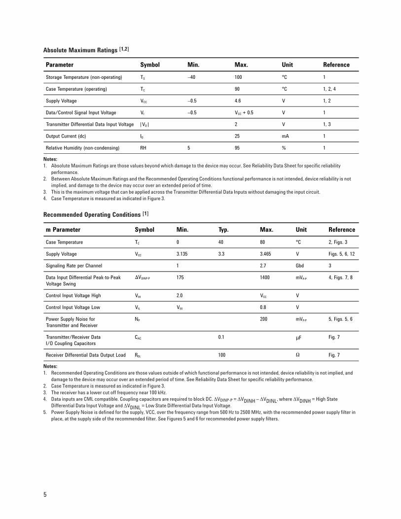
Parameter Symbol Min. Max. Unit Reference
Storage Temperature (non-operating) TS –40 100 °C 1
Case Temperature (operating) TC 90 °C 1, 2, 4
Supply Voltage VCC –0.5 4.6 V 1, 2
Data/Control Signal Input Voltage VI –0.5 VCC + 0.5 V 1
Transmitter Differential Data Input Voltage |VD| 2 V 1, 3
Output Current (dc) ID 25 mA 1
Relative Humidity (non-condensing) RH 5 95 % 1
m Parameter Symbol Min. Typ. Max. Unit Reference
Case Temperature TC 0 40 80 °C 2, Figs. 3
Supply Voltage VCC 3.135 3.3 3.465 V Figs. 5, 6, 12
Signaling Rate per Channel 1 2.7 Gbd 3
Data Input Differential Peak-to-PeakVoltage Swing
DVDINP-P 175 1400 mVP-P 4, Figs. 7, 8
Control Input Voltage High VIH 2.0 VCC V
Control Input Voltage Low VIL VEE 0.8 V
Power Supply Noise forTransmitter and Receiver
NP 200 mVP-P 5, Figs. 5, 6
Transmitter/Receiver DataI/O Coupling Capacitors
CAC 0.1 µF Fig. 7
Receiver Differential Data Output Load RDL 100 W Fig. 7
Notes:1. Recommended Operating Conditions are those values outside of which functional performance is not intended, device reliability is not implied, and
damage to the device may occur over an extended period of time. See Reliability Data Sheet for specific reliability performance.2. Case Temperature is measured as indicated in Figure 3.3. The receiver has a lower cut off frequency near 100 kHz.4. Data inputs are CML compatible. Coupling capacitors are required to block DC. ∆VDINP-P = ∆VDINH – ∆VDINL, where ∆VDINH = High State
Differential Data Input Voltage and ∆VDINL = Low State Differential Data Input Voltage.5. Power Supply Noise is defined for the supply, VCC, over the frequency range from 500 Hz to 2500 MHz, with the recommended power supply filter in
place, at the supply side of the recommended filter. See Figures 5 and 6 for recommended power supply filters.
Notes:1. Absolute Maximum Ratings are those values beyond which damage to the device may occur. See Reliability Data Sheet for specific reliability
performance.2. Between Absolute Maximum Ratings and the Recommended Operating Conditions functional performance is not intended, device reliability is not
implied, and damage to the device may occur over an extended period of time.3. This is the maximum voltage that can be applied across the Transmitter Differential Data Inputs without damaging the input circuit.4. Case Temperature is measured as indicated in Figure 3.
Absolute Maximum Ratings [1,2]
Recommended Operating Conditions [1]
6
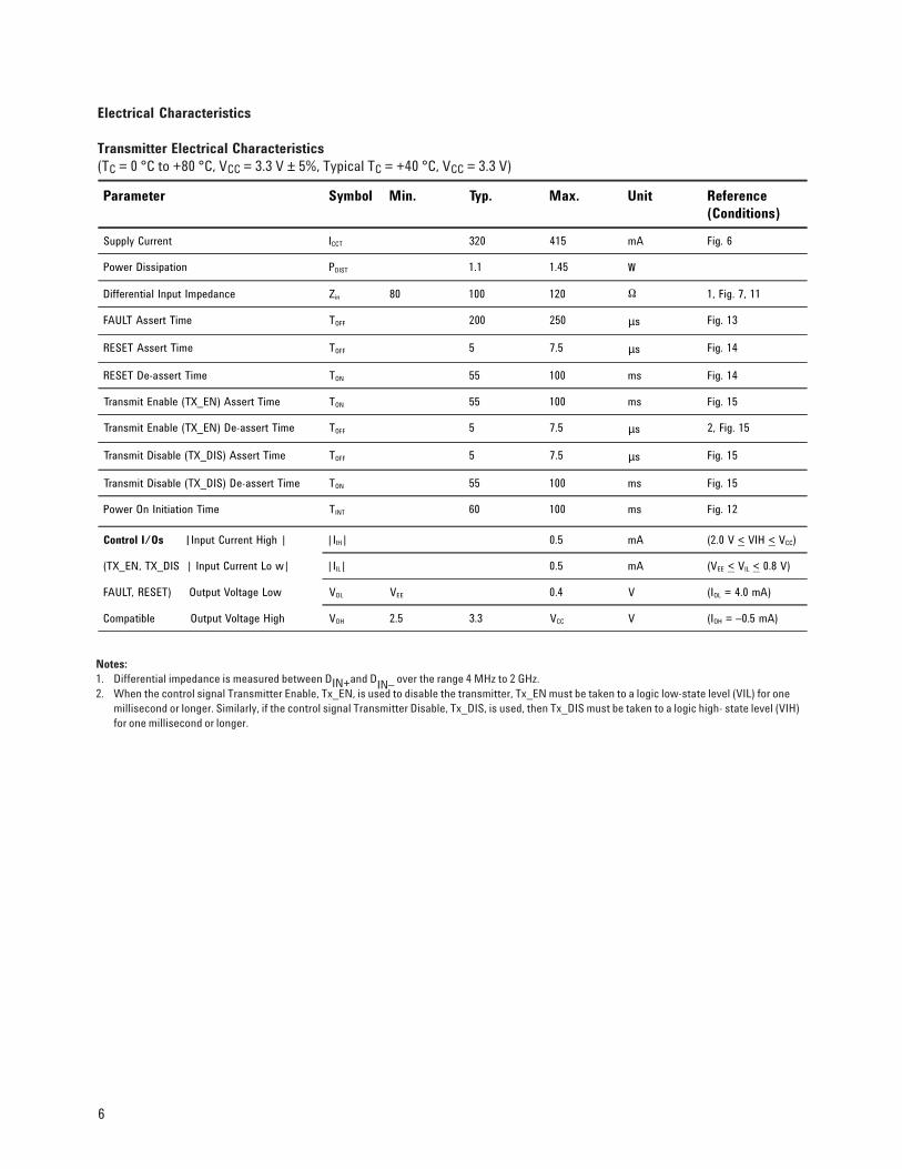
Electrical Characteristics
Transmitter Electrical Characteristics(TC = 0 °C to +80 °C, VCC = 3.3 V ± 5%, Typical TC = +40 °C, VCC = 3.3 V)
Parameter Symbol Min. Typ. Max. Unit Reference(Conditions)
Supply Current ICCT 320 415 mA Fig. 6
Power Dissipation PDIST 1.1 1.45 W
Differential Input Impedance Zin 80 100 120 W 1, Fig. 7, 11
FAULT Assert Time TOFF 200 250 µs Fig. 13
RESET Assert Time TOFF 5 7.5 µs Fig. 14
RESET De-assert Time TON 55 100 ms Fig. 14
Transmit Enable (TX_EN) Assert Time TON 55 100 ms Fig. 15
Transmit Enable (TX_EN) De-assert Time TOFF 5 7.5 µs 2, Fig. 15
Transmit Disable (TX_DIS) Assert Time TOFF 5 7.5 µs Fig. 15
Transmit Disable (TX_DIS) De-assert Time TON 55 100 ms Fig. 15
Power On Initiation Time TINT 60 100 ms Fig. 12
Control I/Os |Input Current High | |IIH| 0.5 mA (2.0 V < VIH < VCC)
(TX_EN, TX_DIS | Input Current Lo w| |IIL| 0.5 mA (VEE < VIL < 0.8 V)
FAULT, RESET) Output Voltage Low VOL VEE 0.4 V (IOL = 4.0 mA)
Compatible Output Voltage High VOH 2.5 3.3 VCC V (IOH = –0.5 mA)
Notes:1. Differential impedance is measured between DIN+and DIN– over the range 4 MHz to 2 GHz.2. When the control signal Transmitter Enable, Tx_EN, is used to disable the transmitter, Tx_EN must be taken to a logic low-state level (VIL) for one
millisecond or longer. Similarly, if the control signal Transmitter Disable, Tx_DIS, is used, then Tx_DIS must be taken to a logic high- state level (VIH)for one millisecond or longer.
7
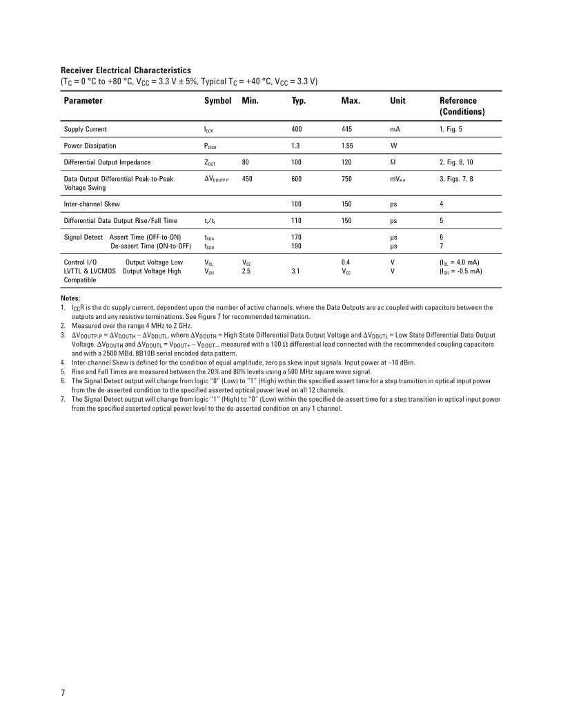
Receiver Electrical Characteristics(TC = 0 °C to +80 °C, VCC = 3.3 V ± 5%, Typical TC = +40 °C, VCC = 3.3 V)
Parameter Symbol Min. Typ. Max. Unit Reference(Conditions)
Supply Current ICCR 400 445 mA 1, Fig. 5
Power Dissipation PDISR 1.3 1.55 W
Differential Output Impedance ZOUT 80 100 120 W 2, Fig. 8, 10
Data Output Differential Peak-to-PeakVoltage Swing
DVDOUTP-P 450 600 750 mVP-P 3, Figs. 7, 8
Inter-channel Skew 100 150 ps 4
Differential Data Output Rise/Fall Time tr/tf 110 150 ps 5
Signal Detect Assert Time (OFF-to-ON) De-assert Time (ON-to-OFF)
tSDA
tSDD
170190
µsµs
67
Control I/O Output Voltage LowLVTTL & LVCMOS Output Voltage HighCompatible
VOL
VOH
VEE
2.5 3.10.4VCC
VV
(IOL = 4.0 mA)(IOH = -0.5 mA)
Notes:1. ICCR is the dc supply current, dependent upon the number of active channels, where the Data Outputs are ac coupled with capacitors between the
outputs and any resistive terminations. See Figure 7 for recommended termination.2. Measured over the range 4 MHz to 2 GHz.3. DVDOUTP-P = DVDOUTH – DVDOUTL, where DVDOUTH = High State Differential Data Output Voltage and DVDOUTL = Low State Differential Data Output
Voltage. DVDOUTH and DVDOUTL = VDOUT+ – VDOUT–, measured with a 100 W differential load connected with the recommended coupling capacitorsand with a 2500 MBd, 8B10B serial encoded data pattern.
4. Inter-channel Skew is defined for the condition of equal amplitude, zero ps skew input signals. Input power at –10 dBm.5. Rise and Fall Times are measured between the 20% and 80% levels using a 500 MHz square wave signal.6. The Signal Detect output will change from logic “0” (Low) to “1” (High) within the specified assert time for a step transition in optical input power
from the de-asserted condition to the specified asserted optical power level on all 12 channels.7. The Signal Detect output will change from logic “1” (High) to “0” (Low) within the specified de-assert time for a step transition in optical input power
from the specified asserted optical power level to the de-asserted condition on any 1 channel.
8
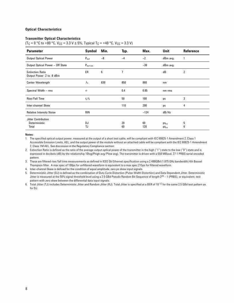
Optical Characteristics
Transmitter Optical Characteristics(TC = 0 °C to +80 °C, VCC = 3.3 V ± 5%, Typical TC = +40 °C, VCC = 3.3 V)
Parameter Symbol Min. Typ. Max. Unit Reference
Output Optical Power POUT –8 –4 –2 dBm avg. 1
Output Optical Power – Off State POUT DIS –30 dBm avg.
Extinction RatioOutput Power -2 to -8 dBm
ER 6 7 dB 2
Center Wavelength lC 830 850 860 nm
Spectral Width – rms s 0.4 0.85 nm rms
Rise/Fall Time tr/tf 50 100 ps 3
Inter-channel Skew 110 200 ps 4
Relative Intensity Noise RIN –124 dB/Hz
Jitter Contribution Deterministic Total
DJTJ
2060
60120
psp-p
psp-p
56
Notes:1. The specified optical output power, measured at the output of a short test cable, will be compliant with IEC 60825-1 Amendment 2, Class 1
Accessible Emission Limits, AEL, and the output power of the module without an attached cable will be compliant with the IEC 60825-1 Amendment2, Class 1M AEL. See discussion in the Regulatory Compliance section.
2. Extinction Ratio is defined as the ratio of the average output optical power of the transmitter in the high (“1”) state to the low (“0”) state and isexpressed in decibels (dB) by the relationship 10log(Phigh avg/Plow avg). The transmitter is driven with a 550 MBaud, 27-1 PRBS serial encodedpattern.
3. These are filtered rise/fall time measurements as defined in IEEE Gb Ethernet specification using a 2.488GBd (1.875 GHz bandwidth) 4th BesselThompson filter. A max spec of 100ps for unfiltered waveform is equivalent to a max spec 215ps for filtered waveform.
4. Inter-channel Skew is defined for the condition of equal amplitude, zero ps skew input signals.5. Deterministic Jitter (DJ) is defined as the combination of Duty Cycle Distortion (Pulse-Width Distortion) and Data Dependent Jitter. Deterministic
Jitter is measured at the 50% signal threshold level using a 2.5 GBd Pseudo Random Bit Sequence of length 223 – 1 (PRBS), or equivalent, testpattern with zero skew between the differential data input signals.
6. Total Jitter (TJ) includes Deterministic Jitter and Random Jitter (RJ). Total Jitter is specified at a BER of 10-12 for the same 2.5 GBd test pattern asfor DJ.
9
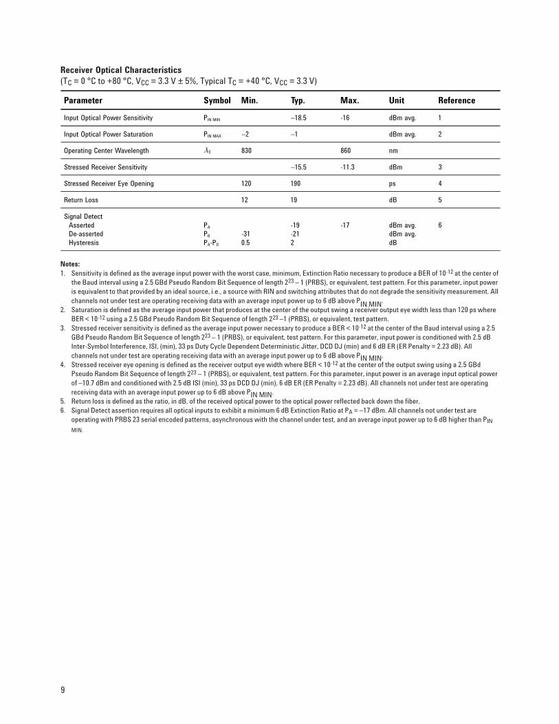
Receiver Optical Characteristics(TC = 0 °C to +80 °C, VCC = 3.3 V ± 5%, Typical TC = +40 °C, VCC = 3.3 V)
Parameter Symbol Min. Typ. Max. Unit Reference
Input Optical Power Sensitivity PIN MIN –18.5 -16 dBm avg. 1
Input Optical Power Saturation PIN MAX –2 –1 dBm avg. 2
Operating Center Wavelength lC 830 860 nm
Stressed Receiver Sensitivity –15.5 -11.3 dBm 3
Stressed Receiver Eye Opening 120 190 ps 4
Return Loss 12 19 dB 5
Signal Detect Asserted De-asserted Hysteresis
PA
PD
PA-PD
-310.5
-19-212
-17 dBm avg.dBm avg.dB
6
Notes:1. Sensitivity is defined as the average input power with the worst case, minimum, Extinction Ratio necessary to produce a BER of 10-12 at the center of
the Baud interval using a 2.5 GBd Pseudo Random Bit Sequence of length 223 – 1 (PRBS), or equivalent, test pattern. For this parameter, input poweris equivalent to that provided by an ideal source, i.e., a source with RIN and switching attributes that do not degrade the sensitivity measurement. Allchannels not under test are operating receiving data with an average input power up to 6 dB above PIN MIN.
2. Saturation is defined as the average input power that produces at the center of the output swing a receiver output eye width less than 120 ps whereBER < 10-12 using a 2.5 GBd Pseudo Random Bit Sequence of length 223 –1 (PRBS), or equivalent, test pattern.
3. Stressed receiver sensitivity is defined as the average input power necessary to produce a BER < 10-12 at the center of the Baud interval using a 2.5GBd Pseudo Random Bit Sequence of length 223 – 1 (PRBS), or equivalent, test pattern. For this parameter, input power is conditioned with 2.5 dBInter-Symbol Interference, ISI, (min), 33 ps Duty Cycle Dependent Deterministic Jitter, DCD DJ (min) and 6 dB ER (ER Penalty = 2.23 dB). Allchannels not under test are operating receiving data with an average input power up to 6 dB above PIN MIN.
4. Stressed receiver eye opening is defined as the receiver output eye width where BER < 10-12 at the center of the output swing using a 2.5 GBdPseudo Random Bit Sequence of length 223 – 1 (PRBS), or equivalent, test pattern. For this parameter, input power is an average input optical powerof –10.7 dBm and conditioned with 2.5 dB ISI (min), 33 ps DCD DJ (min), 6 dB ER (ER Penalty = 2.23 dB). All channels not under test are operatingreceiving data with an average input power up to 6 dB above PIN MIN.
5. Return loss is defined as the ratio, in dB, of the received optical power to the optical power reflected back down the fiber.6. Signal Detect assertion requires all optical inputs to exhibit a minimum 6 dB Extinction Ratio at PA = –17 dBm. All channels not under test are
operating with PRBS 23 serial encoded patterns, asynchronous with the channel under test, and an average input power up to 6 dB higher than PIN
MIN.
10
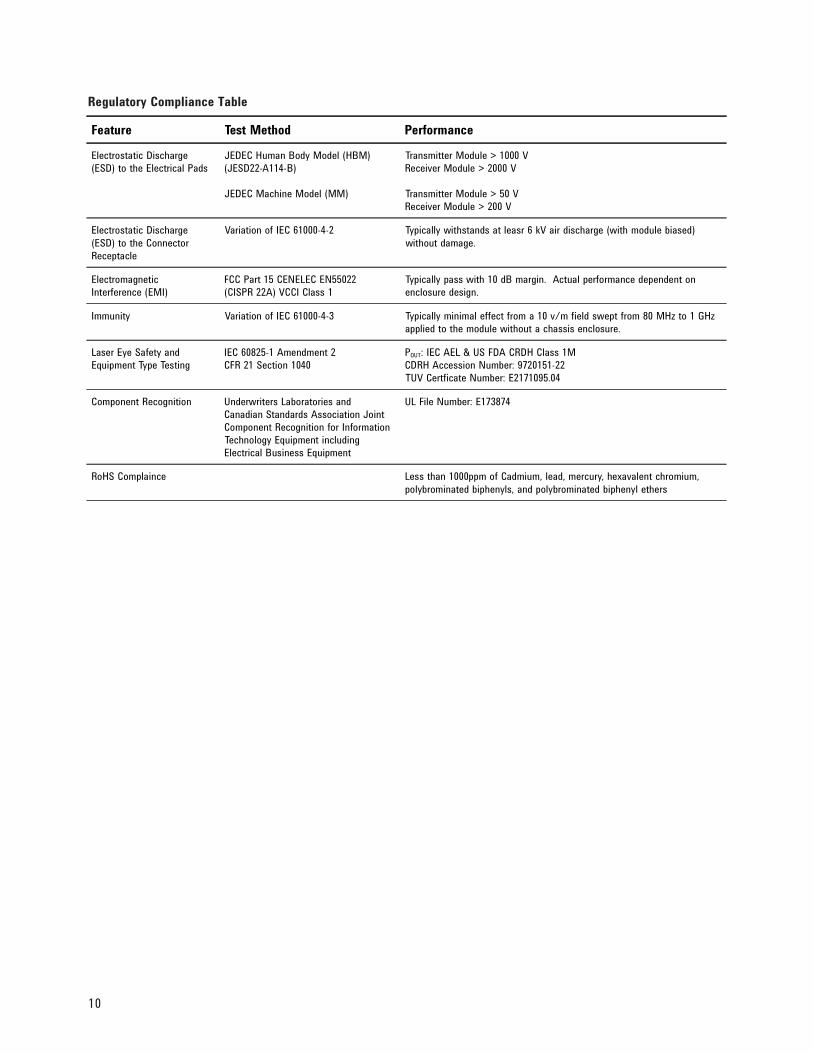
Feature Test Method Performance
Electrostatic Discharge(ESD) to the Electrical Pads
JEDEC Human Body Model (HBM)(JESD22-A114-B)
JEDEC Machine Model (MM)
Transmitter Module > 1000 VReceiver Module > 2000 V
Transmitter Module > 50 VReceiver Module > 200 V
Electrostatic Discharge(ESD) to the ConnectorReceptacle
Variation of IEC 61000-4-2 Typically withstands at leasr 6 kV air discharge (with module biased)without damage.
ElectromagneticInterference (EMI)
FCC Part 15 CENELEC EN55022(CISPR 22A) VCCI Class 1
Typically pass with 10 dB margin. Actual performance dependent onenclosure design.
Immunity Variation of IEC 61000-4-3 Typically minimal effect from a 10 v/m field swept from 80 MHz to 1 GHzapplied to the module without a chassis enclosure.
Laser Eye Safety andEquipment Type Testing
IEC 60825-1 Amendment 2CFR 21 Section 1040
POUT: IEC AEL & US FDA CRDH Class 1MCDRH Accession Number: 9720151-22TUV Certficate Number: E2171095.04
Component Recognition Underwriters Laboratories andCanadian Standards Association JointComponent Recognition for InformationTechnology Equipment includingElectrical Business Equipment
UL File Number: E173874
RoHS Complaince Less than 1000ppm of Cadmium, lead, mercury, hexavalent chromium,polybrominated biphenyls, and polybrominated biphenyl ethers
Regulatory Compliance Table
11
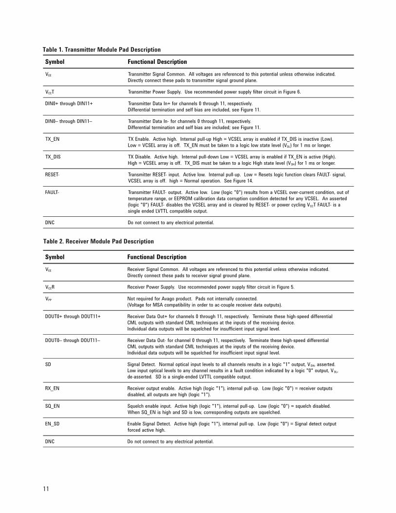
Table 1. Transmitter Module Pad Description
Symbol Functional Description
VEE Transmitter Signal Common. All voltages are referenced to this potential unless otherwise indicated.Directly connect these pads to transmitter signal ground plane.
VCCT Transmitter Power Supply. Use recommended power supply filter circuit in Figure 6.
DIN0+ through DIN11+ Transmitter Data In+ for channels 0 through 11, respectively.Differential termination and self bias are included, see Figure 11.
DIN0– through DIN11– Transmitter Data In- for channels 0 through 11, respectively.Differential termination and self bias are included; see Figure 11.
TX_EN TX Enable. Active high. Internal pull-up High = VCSEL array is enabled if TX_DIS is inactive (Low).Low = VCSEL array is off. TX_EN must be taken to a logic low state level (VOL) for 1 ms or longer.
TX_DIS TX Disable. Active high. Internal pull-down Low = VCSEL array is enabled if TX_EN is active (High).High = VCSEL array is off. TX_DIS must be taken to a logic High state level (VOH) for 1 ms or longer.
RESET- Transmitter RESET- input. Active low. Internal pull-up. Low = Resets logic function clears FAULT- signal,VCSEL array is off. high = Normal operation. See Figure 14.
FAULT- Transmitter FAULT- output. Active low. Low (logic "0") results from a VCSEL over-current condition, out oftemperature range, or EEPROM calibration data corruption condition detected for any VCSEL. An asserted(logic "0") FAULT- disables the VCSEL array and is cleared by RESET- or power cycling VCCT FAULT- is asingle ended LVTTL compatible output.
DNC Do not connect to any electrical potential.
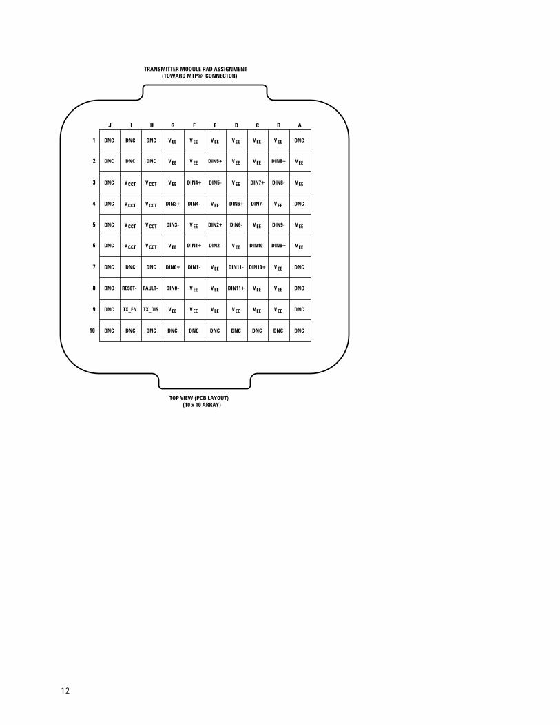
Symbol Functional Description
VEE Receiver Signal Common. All voltages are referenced to this potential unless otherwise indicated.Directly connect these pads to receiver signal ground plane.
VCCR Receiver Power Supply. Use recommended power supply filter circuit in Figure 5.
VPP Not required for Avago product. Pads not internally connected.(Voltage for MSA compatibility in order to ac-couple receiver data outputs).
DOUT0+ through DOUT11+ Receiver Data Out+ for channels 0 through 11, respectively. Terminate these high-speed differentialCML outputs with standard CML techniques at the inputs of the receiving device.Individual data outputs will be squelched for insufficient input signal level.
DOUT0– through DOUT11– Receiver Data Out- for channel 0 through 11, respectively. Terminate these high-speed differentialCML outputs with standard CML techniques at the inputs of the receiving device.Individual data outputs will be squelched for insufficient input signal level.
SD Signal Detect. Normal optical input levels to all channels results in a logic "1" output, VOH, asserted.Low input optical levels to any channel results in a fault condition indicated by a logic "0" output, VOL,de-asserted. SD is a single-ended LVTTL compatible output.
RX_EN Receiver output enable. Active high (logic "1"), internal pull-up. Low (logic "0") = receiver outputsdisabled, all outputs are high (logic "1").
SQ_EN Squelch enable input. Active high (logic "1"), internal pull-up. Low (logic "0") = squelch disabled.When SQ_EN is high and SD is low, corresponding outputs are squelched.
EN_SD Enable Signal Detect. Active high (logic "1"), internal pull-up. Low (logic "0") = Signal detect outputforced active high.
DNC Do not connect to any electrical potential.
Table 2. Receiver Module Pad Description
12
DNC
J
DNC
I
DNC
H
V EE
G
V EE
F
V EE
E
V EE
D
V EE
C
V EE
B
DNC
A
1
DNC DNC DNC V EE V EE DIN5+ V EE V EE DIN8+ V EE2
DNC V CCT V CCT V EE DIN4+ DIN5- V EE DIN7+ DIN8- V EE3
DNC V CCT V CCT DIN3+ DIN4- V EE DIN6+ DIN7- V EE DNC4
DNC V CCT V CCT DIN3- V EE DIN2+ DIN6- V EE DIN9- V EE5
DNC V CCT V CCT V EE DIN1+ DIN2- V EE DIN10- DIN9+ V EE6
DNC DNC DNC DIN0+ DIN1- V EE DIN11- DIN10+ V EE DNC7
DNC RESET- FAULT- DIN0- V EE V EE DIN11+ V EE V EE DNC8
DNC TX_EN TX_DIS V EE V EE V EE V EE V EE V EE DNC9
DNC DNC DNC DNC DNC DNC DNC DNC DNC DNC10
TRANSMITTER MODULE PAD ASSIGNMENT(TOWARD MTP® CONNECTOR)
TOP VIEW (PCB LAYOUT)(10 x 10 ARRAY)
13
V PP
J
DNC
I
DNC
H
V EE
G
V EE
F
V EE
E
V EE
D
V EE
C
V EE
B
DNC
A
1
V PP DNC DNC V EE V EE DOUT5- V EE V EE DOUT8- V EE2
DNC V CCR V CCR V EE DOUT4- DOUT5+ V EE DOUT7- DOUT8+ V EE3
DNC V CCR V CCR DOUT3- DOUT4+ V EE DOUT6- DOUT7+ V EE DNC4
DNC V CCR V CCR DOUT3+ V EE DOUT2- DOUT6+ V EE DOUT9+ V EE5
DNC V CCR V CCR V EE DOUT1- DOUT2+ V EE DOUT10+ DOUT9- V EE6
DNC DNC SD DOUT0- DOUT1+ V EE DOUT11+ DOUT10- V EE DNC7
V PP DNC DNC DOUT0+ V EE V EE DOUT11- V EE V EE DNC8
V PP RX_EN EN_SD V EE V EE V EE V EE V EE V EE DNC9
SQ_EN DNC DNC DNC DNC DNC DNC DNC DNC DNC10
RECEIVER MODULE PAD ASSIGNMENT(TOWARD MTP® CONNECTOR)
TOP VIEW (PCB LAYOUT)(10 x 10 ARRAY)
14
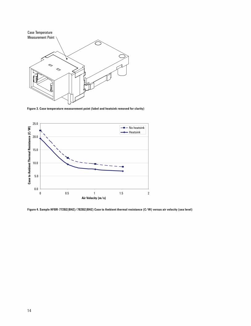
Figure 3. Case temperature measurement point (label and heatsink removed for clarity)
Case TemperatureMeasurement Point
0.0
5.0
10.0
15.0
20.0
25.0
0 0.5 1 1.5 2
Air Velocity (m/s)
Cas
e to
Am
bien
t The
rmal
Res
ista
nce
(C/W
) No heatsinkHeatsink
Figure 4. Sample HFBR-772BZ(BHZ)/782BZ(BHZ) Case to Ambient thermal resistance (C/W) versus air velocity (sea level)
15
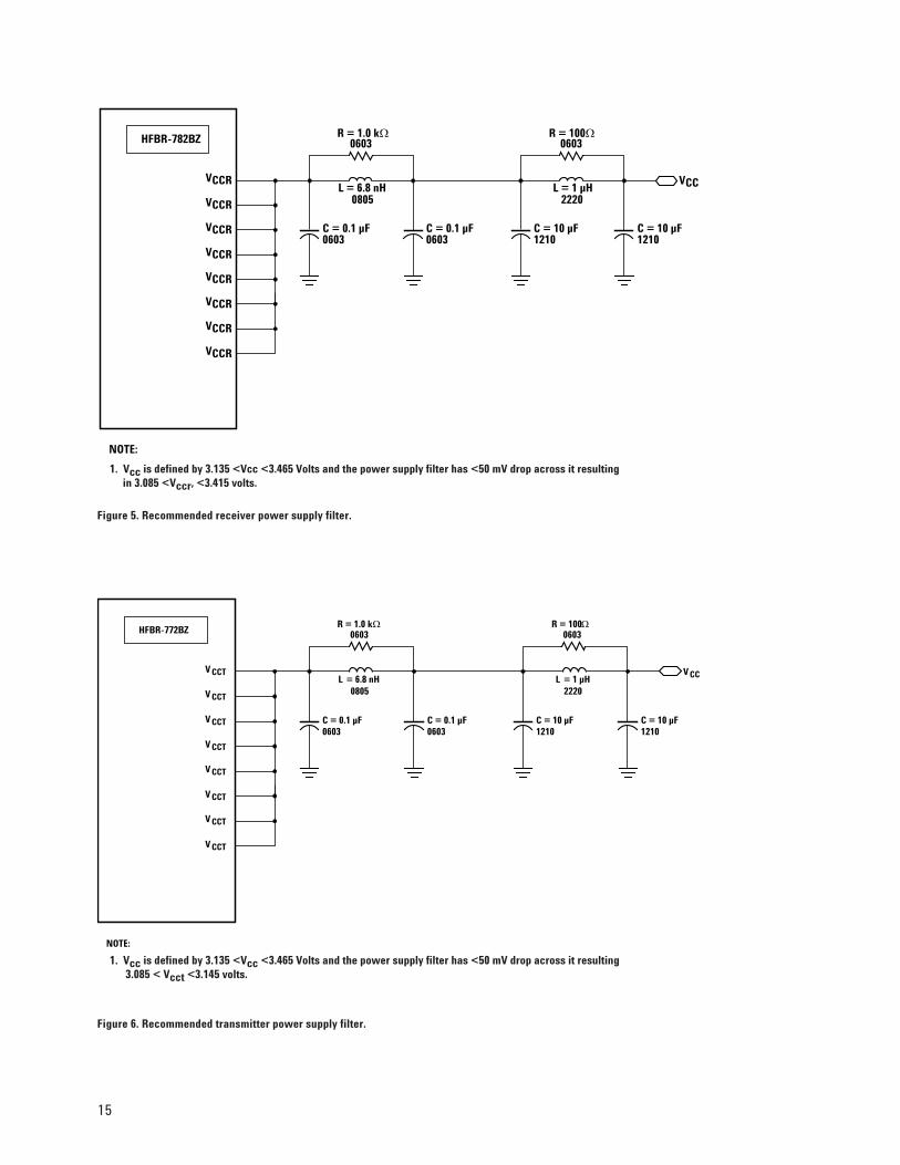
Figure 5. Recommended receiver power supply filter.
VCC
HFBR-782BZ
VCCR
VCCR
VCCR
VCCR
VCCR
VCCR
R = 100 Ω0603
C = 10 µF1210
L = 1 µH 2220
L = 6.8 nH 0805
R = 1.0 k Ω0603
C = 0.1 µF0603
C = 0.1 µF0603
C = 10 µF1210
VCCR
VCCR
NOTE:
1. Vcc is defined by 3.135 <Vcc <3.465 Volts and the power supply filter has <50 mV drop across it resulting in 3.085 <Vccr, <3.415 volts.
V CC
HFBR-772BZR = 100 Ω
0603
C = 10 µF1210
L = 1 µH 2220
L = 6.8 nH 0805
R = 1.0 kΩ0603
C = 0.1 µF0603
C = 0.1 µF0603
C = 10 µF1210
NOTE:
V CCT
V CCT
V CCT
V CCT
V CCT
V CCT
V CCT
V CCT
1. Vcc is defined by 3.135 <Vcc <3.465 Volts and the power supply filter has <50 mV drop across it resulting 3.085 < Vcct <3.145 volts.
Figure 6. Recommended transmitter power supply filter.
16
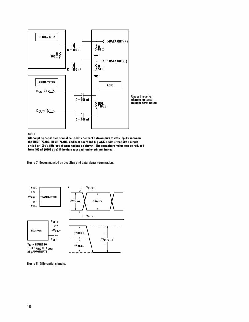
Figure 7. Recommended ac coupling and data signal termination.
NOTE:AC coupling capacitors should be used to connect data outputs to data inputs betweenthe HFBR-772BZ, HFBR-782BZ, and host board ICs (eg ASIC) with either 50 Ω singleended or 100 Ω differential terminations as shown. The capacitors' value can be reducedfrom 100 nF (0603 size) if the data rate and run length are limited.
DATA OUT (+)HFBR-772BZ
R50 Ω
DATA OUT (–)
R50 Ω
R100 Ω
ASICHFBR-782BZ
RDL100 Ω
DOUT (+)
DOUT (–)
C = 100 nF
C = 100 nF
C = 100 nF
C = 100 nF
Unused receiverchannel outputsmust be terminated
D IN+
D IN–
TRANSMITTER∆V DIN
–
+
D OUT+
D OUT–
RECEIVER
–
+
∆V DOUT
∆V DI/OH ∆V DI/OL
V DI/O+
V DI/O–
∆V DI/O P-P
∆V DI/OL–
+∆V DI/OH
V DI/O REFERS TOEITHER VDIN OR VDOUTAS APPROPRIATE
Figure 8. Differential signals.

17
Figure 9. Package board footprint (dimensions in mm). PCB top view.
Note: The host electrical connector attached to the PCB must be a 100-position FCI Meg-Array Plug (FCI PN: 84512-102) or equivalent.
2 x ∅ 2.54 MIN. PAD KEEP-OUT
18.42 MIN.
13.72
50KEEP-OUT AREA
FOR MPO CONNECTOR
5.46
30.23
1.89 REF.
8.00
9 x 1.27 TOT = 11.43
8.95 REF.
FRONT
SYM.
9 x 1.27 TOT = 11.43
18 REF.
SYM.
END OFMODULE
2 x ∅ 1.7 ± 0.05 HOLES
3 x ∅ 4.17 MIN. PAD KEEP-OUT
3 x ∅ 2.69 ± 0.05 HOLESFOR #2 SCREW
(10 x 10 =) 100 x ∅ 0.58 ± 0.05 PADS
PCB LAYOUT(TOP VIEW)
100 PIN FCIMEG-Array® RECEPTACLE
CONNECT ORS
Rx
Tx
∅ 0.1 A B-C
∅ 0.1 A B-C
∅ 0.1 A B-C
∅ 0.1 A B-C
B
A
C
∅ 0.05 A B-C
18
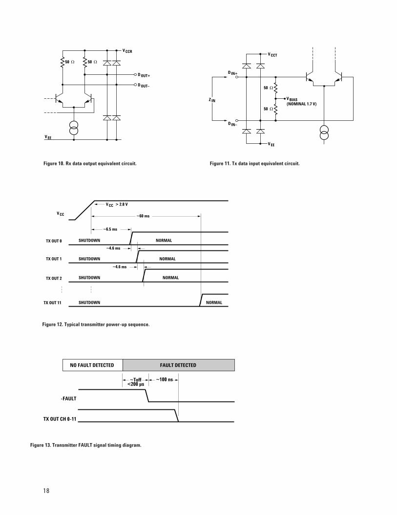
Figure 10. Rx data output equivalent circuit. Figure 11. Tx data input equivalent circuit.
V CC
TX OUT 0
TX OUT 1
TX OUT 2
TX OUT 11
~6.5 ms
~60 ms
V CC > 2.8 V
SHUTDOWN
SHUTDOWN
SHUTDOWN
SHUTDOWN
NORMAL
NORMAL
NORMAL
NORMAL
~4.6 ms
~4.6 ms
-FAULT
~100 ns~Toff<200 µs
TX OUT CH 0-11
NO FAULT DETECTED FAULT DETECTED
V CCR
50 Ω50 Ω
V EE
D OUT+
D OUT–
D IN+
50 Ω
D IN–
50 Ω
Z IN V BIAS(NOMINAL 1.7 V)
V CCT
V EE
Figure 13. Transmitter FAULT signal timing diagram.
Figure 12. Typical transmitter power-up sequence.
19
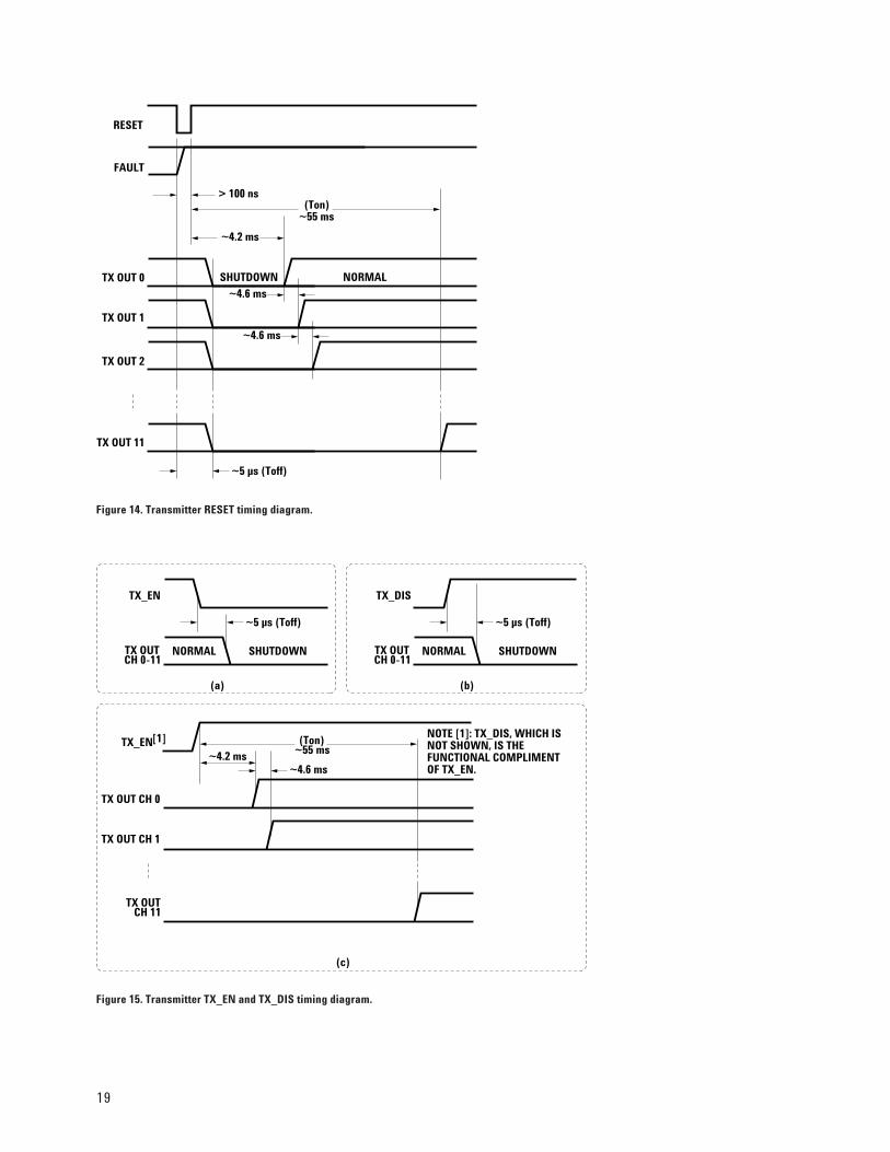
Figure 14. Transmitter RESET timing diagram.
TX OUT 0
TX OUT 1
TX OUT 2
TX OUT 11
~4.2 ms
(Ton)~55 ms
SHUTDOWN NORMAL
~4.6 ms
~4.6 ms
> 100 ns
~5 µs (Toff)
FAULT
RESET
TX OUT CH 0
TX OUT CH 1
TX OUTCH 11
~4.2 ms(Ton)
~55 ms
~4.6 ms
TX_EN
~5 µs (Toff)
SHUTDOWNNORMALTX OUTCH 0-11
(a)
TX_DIS
~5 µs (Toff)
SHUTDOWNNORMALTX OUTCH 0-11
(b)
TX_EN[1] NOTE [1]: TX_DIS, WHICH IS NOT SHOWN, IS THEFUNCTIONAL COMPLIMENT OF TX_EN.
(c)
Figure 15. Transmitter TX_EN and TX_DIS timing diagram.
20
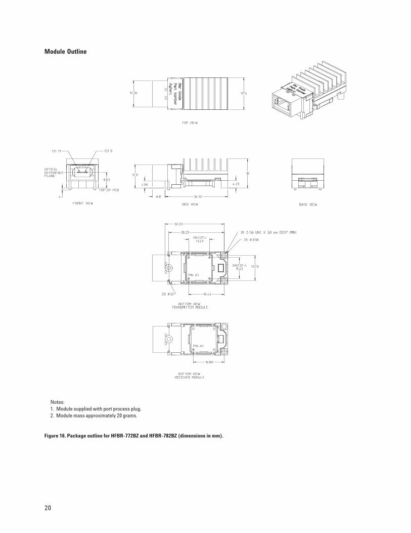
Module Outline
Figure 16. Package outline for HFBR-772BZ and HFBR-782BZ (dimensions in mm).
Notes:1. Module supplied with port process plug.2. Module mass approximately 20 grams.
21
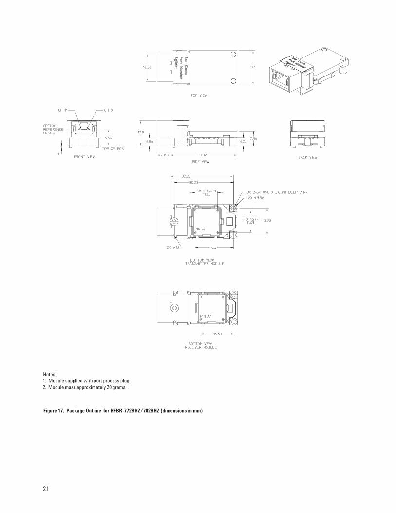
Figure 17. Package Outline for HFBR-772BHZ/782BHZ (dimensions in mm)
Notes:1. Module supplied with port process plug.2. Module mass approximately 20 grams.
22
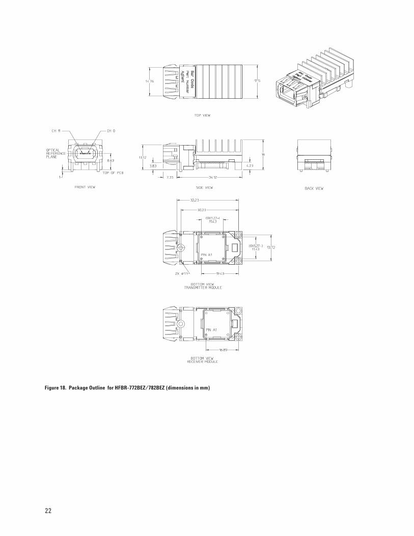
Figure 18. Package Outline for HFBR-772BEZ/782BEZ (dimensions in mm)
23
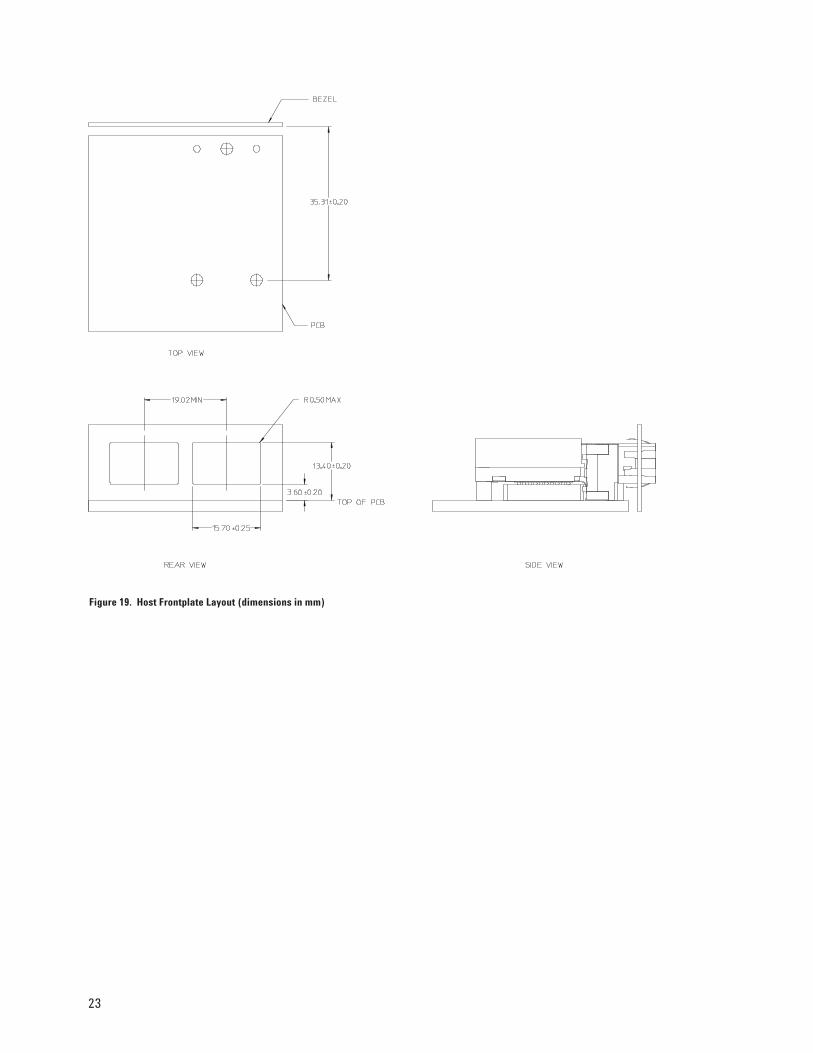
Figure 19. Host Frontplate Layout (dimensions in mm)

For product information and a complete list of distributors, please go to our web site: www.avagotech.com
Avago, Avago Technologies, and the A logo are trademarks of Avago Technologies, Pte. in the United States and other countries.Data subject to change. Copyright © 2005 Avago Technologies Pte. All rights reserved.5989-4520EN - December 14, 2005