Embed Size (px)
Citation preview
H. Buhmann H. Buhmann
Hartmut Buhmann
Physikalisches Institut, EP3
Universität Würzburg
Germany
H. Buhmann H. Buhmann
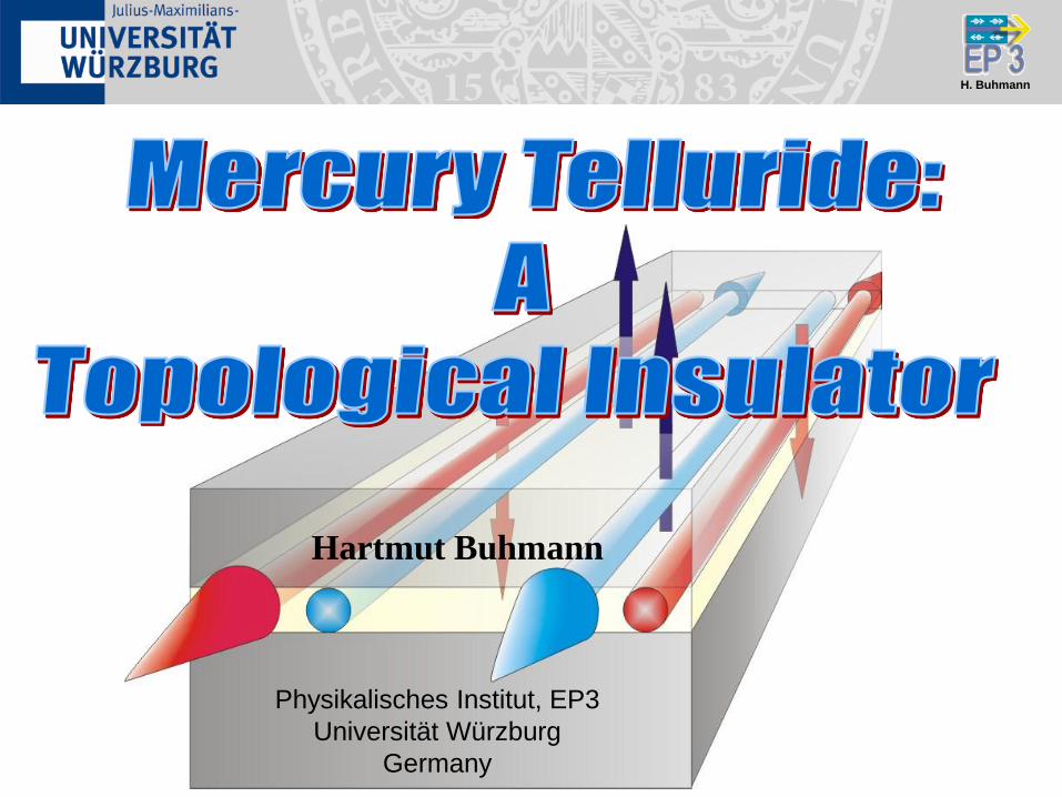
TV-Series: „The Big Bang Theory“, S04, E14 (2011)
H. Buhmann H. Buhmann
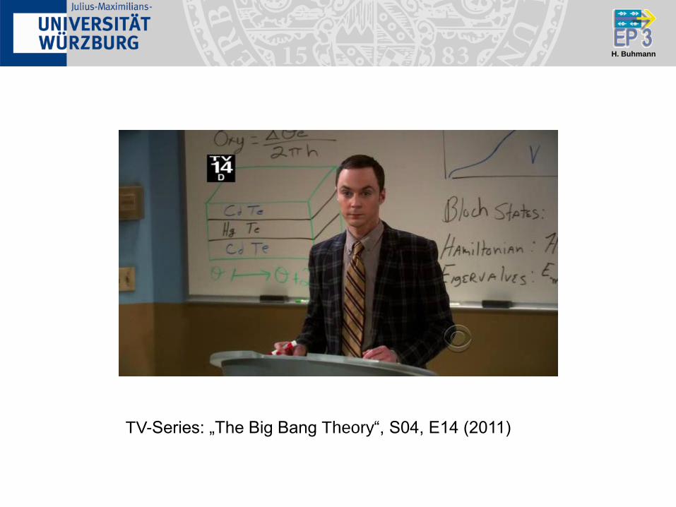
Outline
• Insulators and Topological Insulators
• HgTe
• crystal structure
• quantum wells
Two-Dimensional TI
• Quantum Spin Hall Effect
• quantized conductivity
• non-locality
• spin polarization
• strained layers
Three-Dimensional TI
• quantum Hall effect
• super currents

H. Buhmann
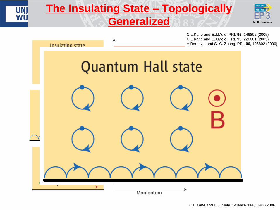
C.L.Kane and E.J. Mele, Science 314, 1692 (2006)
C.L.Kane and E.J.Mele, PRL 95, 146802 (2005)
C.L.Kane and E.J.Mele, PRL 95, 226801 (2005)
A.Bernevig and S.-C. Zhang, PRL 96, 106802 (2006)
The Insulating States
Topologically Generalized
H. Buhmann
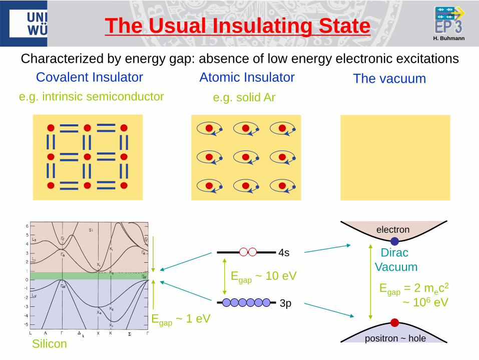
Covalent Insulator
Characterized by energy gap: absence of low energy electronic excitations
The vacuum Atomic Insulator
e.g. solid Ar
Dirac
Vacuum Egap ~ 10 eV
e.g. intrinsic semiconductor
Egap ~ 1 eV
3p
4s
Silicon
Egap = 2 mec2
~ 106 eV
electron
positron ~ hole
The Usual Insulating State
H. Buhmann
C.L.Kane and E.J. Mele, Science 314, 1692 (2006)
C.L.Kane and E.J.Mele, PRL 95, 146802 (2005)
C.L.Kane and E.J.Mele, PRL 95, 226801 (2005)
A.Bernevig and S.-C. Zhang, PRL 96, 106802 (2006)
The Insulating State – Topologically
Generalized

H. Buhmann
2D Cyclotron Motion, Landau Levels
gap cE E
Energy gap bulk insulator
The Integer Quantum Hall State
H. Buhmann
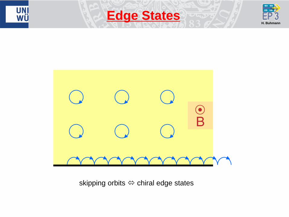
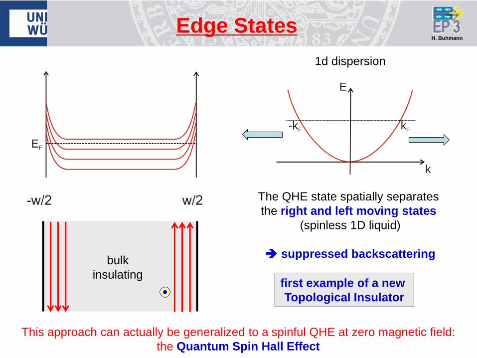
Edge States
skipping orbits chiral edge states
H. Buhmann
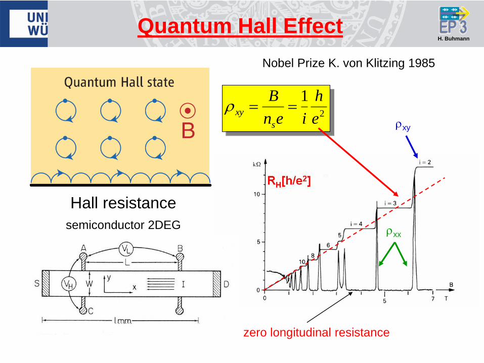
Quantum Hall Effect
Hall resistance
2
1
e
h
ien
B
s
xy xy
xx
zero longitudinal resistance
semiconductor 2DEG
Nobel Prize K. von Klitzing 1985
H. Buhmann
21( ) ( )
2 BZn d u u
i k kk k k
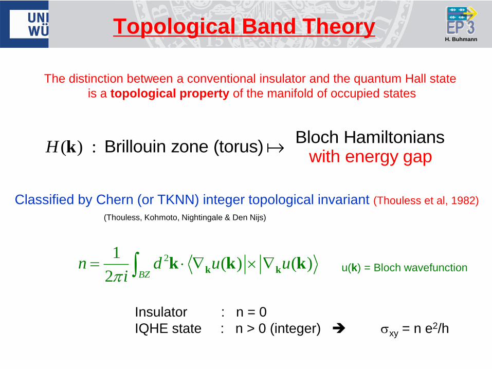
The distinction between a conventional insulator and the quantum Hall state
is a topological property of the manifold of occupied states
Insulator : n = 0
IQHE state : n > 0 (integer) sxy = n e2/h
Classified by Chern (or TKNN) integer topological invariant (Thouless et al, 1982)
( ) :H kBloch Hamiltonians
Brillouiw
n zone (torus) ith energy gap
u(k) = Bloch wavefunction
Topological Band Theory
(Thouless, Kohmoto, Nightingale & Den Nijs)

H. Buhmann
Vacuum
Dn = # Chiral Edge Modes
Edge States
The TKNN invariant can only change with a phase
transition where the energy gap goes to zero
Vacuum
n = 0 n = 3 n = 0
H. Buhmann
bulk
insulating
Edge States
1d dispersion
k
kF-kF
E
The QHE state spatially separates
the right and left moving states
(spinless 1D liquid)
suppressed backscattering
first example of a new
Topological Insulator
This approach can actually be generalized to a spinful QHE at zero magnetic field:
the Quantum Spin Hall Effect
H. Buhmann
C.L.Kane and E.J. Mele, Science 314, 1692 (2006)
C.L.Kane and E.J.Mele, PRL 95, 146802 (2005)
C.L.Kane and E.J.Mele, PRL 95, 226801 (2005)
A.Bernevig and S.-C. Zhang, PRL 96, 106802 (2006)
The Insulating State – Topologically
Generalized

H. Buhmann
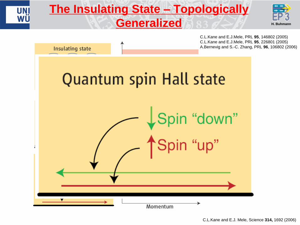
Quantum Spin Hall Effect
effB
effB
Quantum Spin Hall State
consisting of two counter propagating spin
polarized edge channels
and an insulating bulk
broken time reversal symmetry (TRS)
invariant under TR
TR copy
H. Buhmann
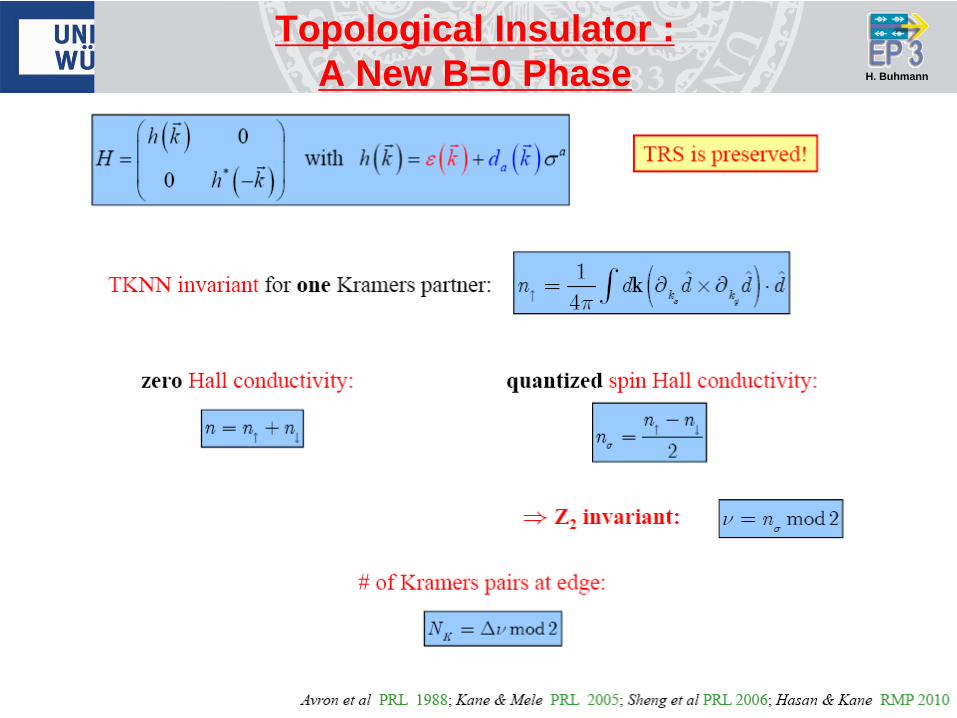
Topological Insulator :
A New B=0 Phase
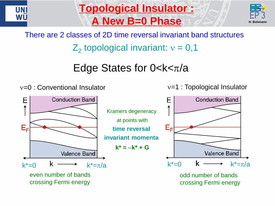
H. Buhmann
There are 2 classes of 2D time reversal invariant band structures
Z2 topological invariant: n = 0,1
n=0 : Conventional Insulator n=1 : Topological Insulator
Kramers degeneracy
at points with
time reversal
invariant momenta
k* = -k* + G
k*=0 k*=/a k*=0 k*=/a
Edge States for 0<k</a
even number of bands
crossing Fermi energy odd number of bands
crossing Fermi energy
Topological Insulator :
A New B=0 Phase

H. Buhmann
There are 4 surface Dirac Points due to Kramers degeneracy
Surface Brillouin Zone
2D Dirac Point
E
k=La k=Lb
E
k=La k=Lb
n0 = 1 : Strong Topological Insulator
Fermi circle encloses odd number of Dirac points
Topological Metal : 1/4 graphene
Berry’s phase
Robust to disorder: impossible to localize
n0 = 0 : Weak Topological Insulator
Related to layered 2D QSHI ; (n1n2n3) ~ Miller indices
Fermi surface encloses even number of Dirac points
OR
L4
L1 L2
L3
EF
How do the Dirac points connect? Determined
by 4 bulk Z2 topological invariants n0 ; (n1n2n3)
kx
ky
kx
ky
kx
ky
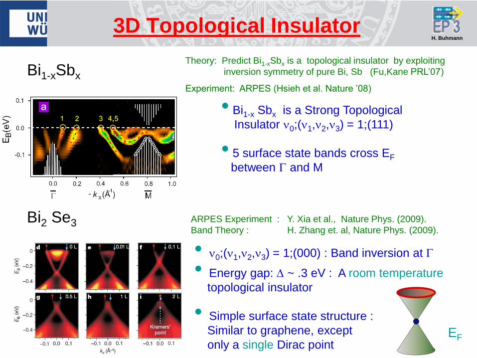
3D Topological Insulator

H. Buhmann H. Buhmann
H. Buhmann
Bi1-xSbx
Theory: Predict Bi1-xSbx is a topological insulator by exploiting
inversion symmetry of pure Bi, Sb (Fu,Kane PRL’07) Experiment: ARPES (Hsieh et al. Nature ’08)
• Bi1-x Sbx is a Strong Topological
Insulator n0;(n1,n2,n3) = 1;(111)
• 5 surface state bands cross EF
between G and M
ARPES Experiment : Y. Xia et al., Nature Phys. (2009).
Band Theory : H. Zhang et. al, Nature Phys. (2009). Bi2 Se3
• n0;(n1,n2,n3) = 1;(000) : Band inversion at G • Energy gap: D ~ .3 eV : A room temperature
topological insulator
• Simple surface state structure :
Similar to graphene, except
only a single Dirac point EF
3D Topological Insulator
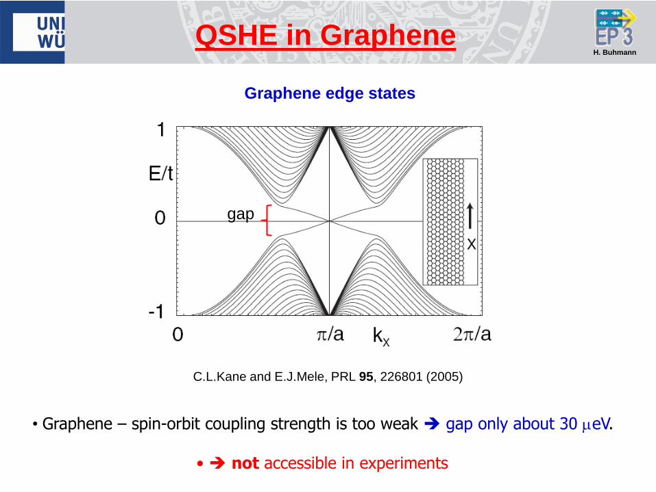
H. Buhmann
C.L.Kane and E.J.Mele, PRL 95, 226801 (2005)
Graphene edge states
QSHE in Graphene
• Graphene – spin-orbit coupling strength is too weak gap only about 30 meV.
• not accessible in experiments
gap

H. Buhmann
QSHE in HgTe
Helical edge states
for inverted HgTe QW
B.A Bernevig, T.L. Hughes, S.C. Zhang, Science 314, 1757 (2006)
k
E
H1
E1
0
DEg = 30…60 meV
(typically)
H. Buhmann
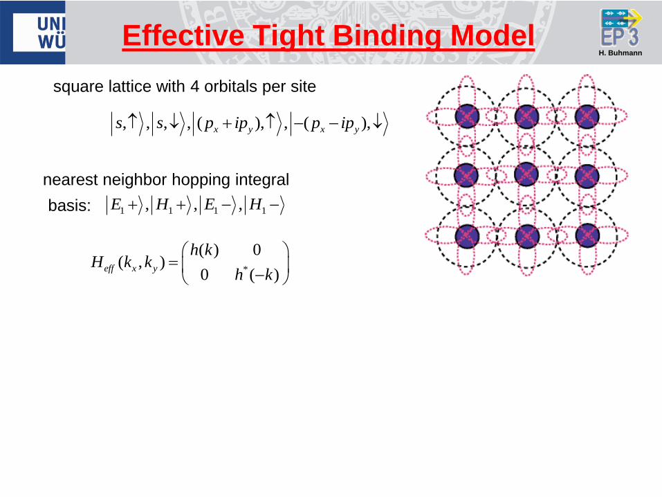
Effective Tight Binding Model
square lattice with 4 orbitals per site
, , , , ( ), , ( ),x y x ys s p ip p ip - -
nearest neighbor hopping integral
basis: 1 1 1 1, , ,E H E H - -
*
( ) 0( , )
0 ( )eff x y
h kH k k
h k
-
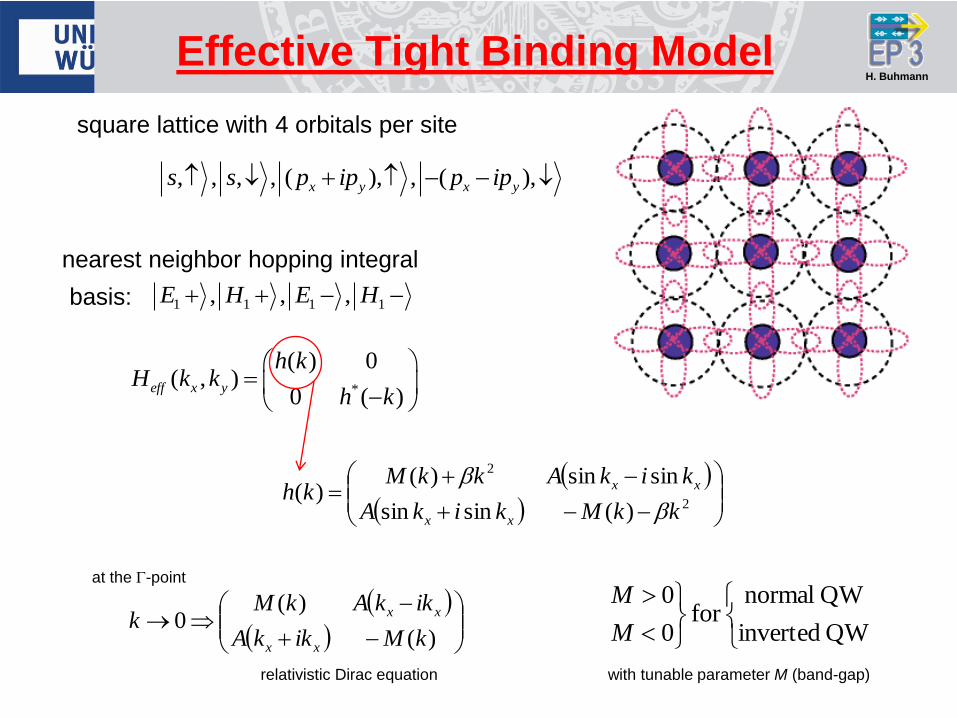
H. Buhmann
Effective Tight Binding Model
square lattice with 4 orbitals per site
, , , , ( ), , ( ),x y x ys s p ip p ip - -
nearest neighbor hopping integral
basis: 1 1 1 1, , ,E H E H - -
*
( ) 0( , )
0 ( )eff x y
h kH k k
h k
-
relativistic Dirac equation with tunable parameter M (band-gap)
at the G-point
--
-
2
2
)(sinsin
sinsin)()(
kkMkikA
kikAkkMkh
xx
xx
-
-
)(
)(0
kMikkA
ikkAkMk
xx
xx
QW inverted
QW normalfor
0
0
M
M
H. Buhmann
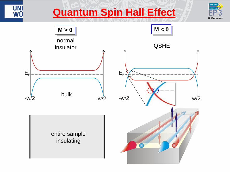
Quantum Spin Hall Effect
normal
insulator
bulk
bulk
insulating
entire sample
insulating
M > 0 M < 0
QSHE
H. Buhmann
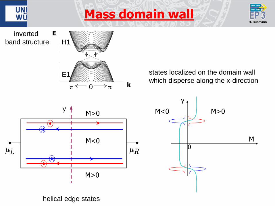
Mass domain wall
states localized on the domain wall
which disperse along the x-direction
M
y
0
M>0
M<0
M>0
y
x
x
M>0 M<0
inverted
band structure
helical edge states
k
E
H1
E1
0
H. Buhmann H. Buhmann
H. Buhmann H. Buhmann
H. Buhmann
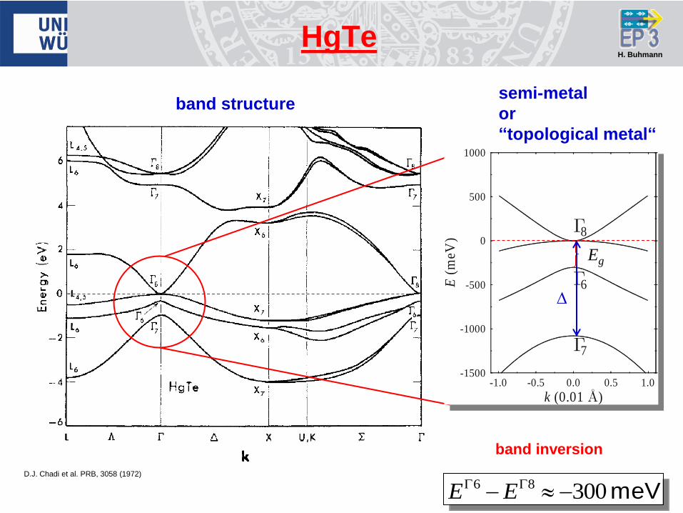
band structure
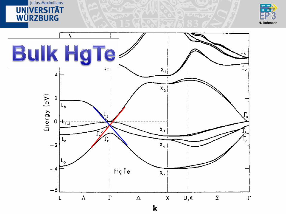
D.J. Chadi et al. PRB, 3058 (1972)
band inversion
meV 30086 -- GG EE
semi-metal
or
“topological metal“
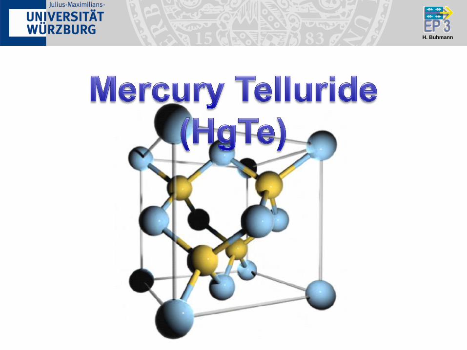
HgTe
-1.0 -0.5 0.0 0.5 1.0
k (0.01 )
-1500
-1000
-500
0
500
1000
E(m
eV) 8
6
7
Eg
D

H. Buhmann
CdTe and HgTe
H = H1 + HD + Hmv + Hso
CdTe HgTe
H. Buhmann
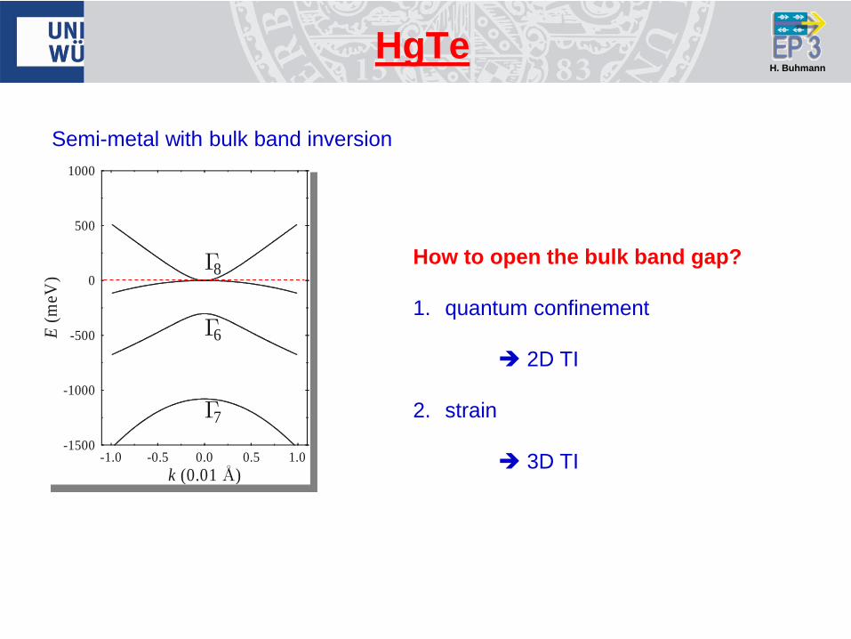
HgTe
-1.0 -0.5 0.0 0.5 1.0
k (0.01 )
-1500
-1000
-500
0
500
1000
E(m
eV) 8
6
7
Semi-metal with bulk band inversion
How to open the bulk band gap?
1. quantum confinement
2D TI
2. strain
3D TI

H. Buhmann H. Buhmann
H. Buhmann
-1.0 -0.5 0.0 0.5 1.0
k (0.01 )
-1500
-1000
-500
0
500
1000
E(m
eV)
HgTe
8
6
7
-1.0 -0.5 0.0 0.5 1.0
k (0.01 )
Hg0.32Cd0.68Te
-1500
-1000
-500
0
500
1000
E(m
eV)
6
8
7
VBO
Barrier QW
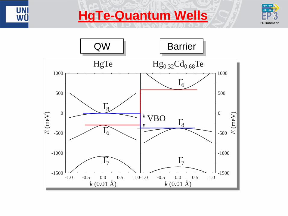
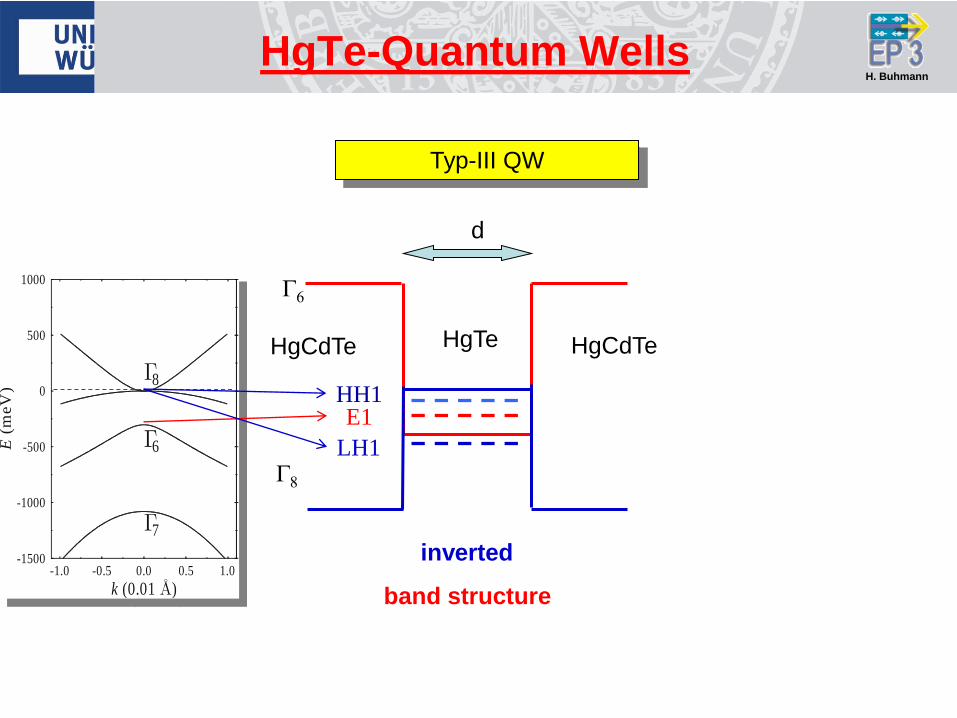
HgTe-Quantum Wells
H. Buhmann
Typ-III QW
band structure
HgCdTe HgTe
G6
G8
inverted
HgTe-Quantum Wells
HgCdTe
HH1 E1
d
-1.0 -0.5 0.0 0.5 1.0
k (0.01 )
-1500
-1000
-500
0
500
1000
E(m
eV
)
8
6
7
LH1
H. Buhmann
Typ-III QW
band structure
HgCdTe HgTe
G6
G8
inverted
HgTe-Quantum Wells
HgCdTe
HH1 E1
d
normal
H. Buhmann
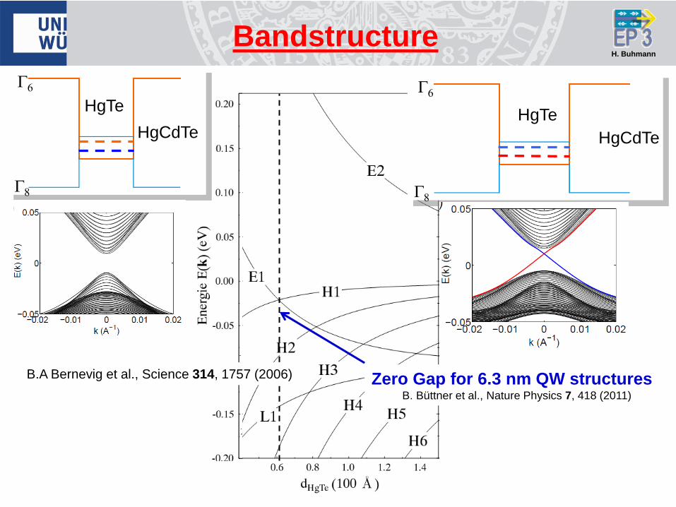
Bandstructure
HgCdTe
HgTe
G6
G8
HgCdTe
HgTe
G6
G8
Zero Gap for 6.3 nm QW structures B. Büttner et al., Nature Physics 7, 418 (2011)
B.A Bernevig et al., Science 314, 1757 (2006)
H. Buhmann H. Buhmann
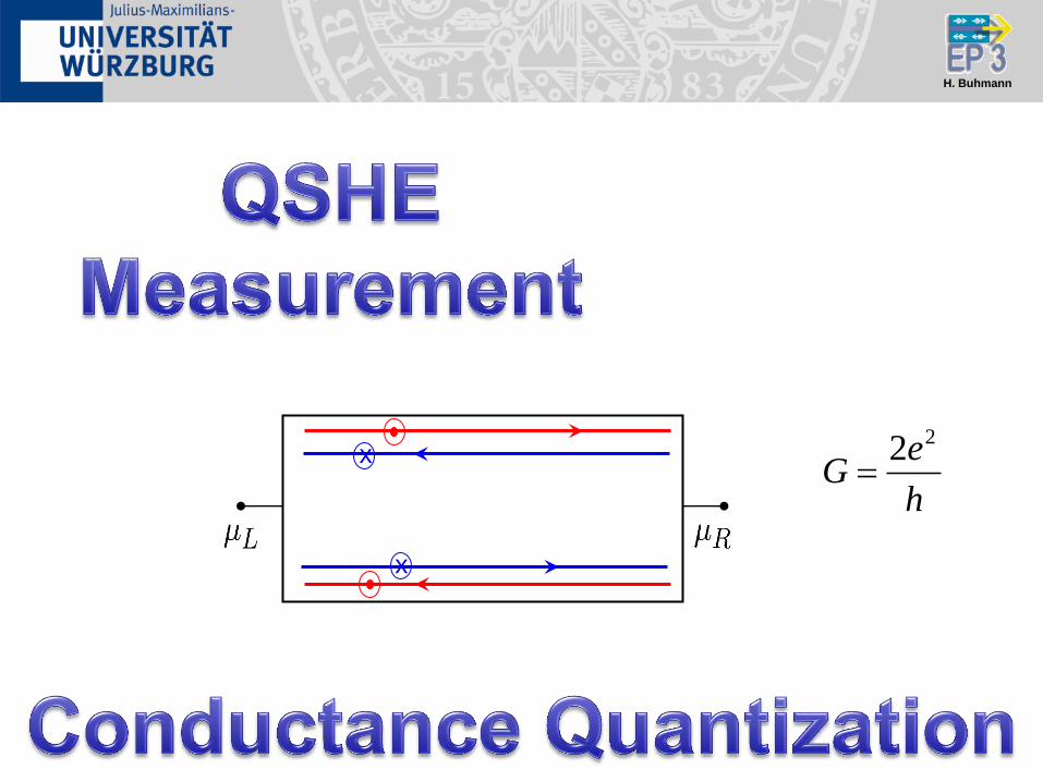
H. Buhmann H. Buhmann
x
x
h
eG
22
H. Buhmann
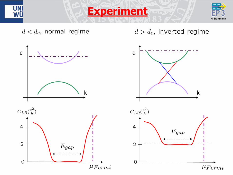
Experiment
k
e
k
e
H. Buhmann
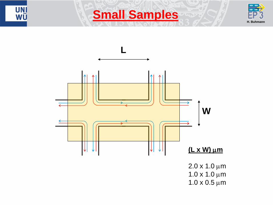
Small Samples
L
W
(L x W) mm
2.0 x 1.0 mm
1.0 x 1.0 mm
1.0 x 0.5 mm
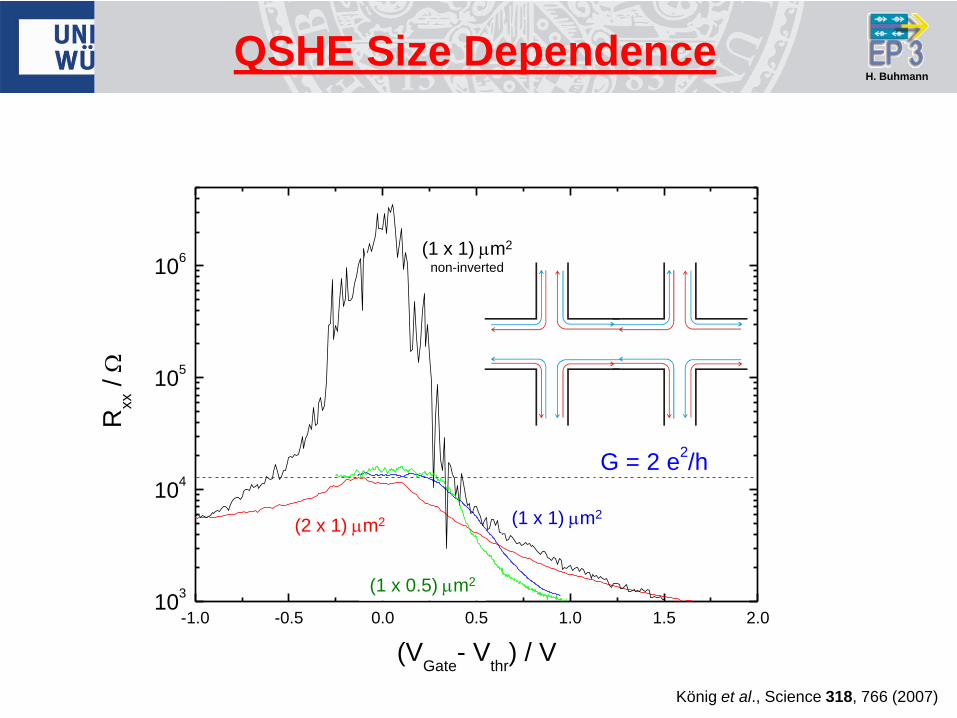
H. Buhmann
-1.0 -0.5 0.0 0.5 1.0 1.5 2.010
3
104
105
106
G = 2 e2/h
Rxx /
(VGate
- Vthr
) / V
QSHE Size Dependence
(1 x 0.5) mm2
(1 x 1) mm2 (2 x 1) mm2
(1 x 1) mm2
non-inverted
König et al., Science 318, 766 (2007)
H. Buhmann H. Buhmann
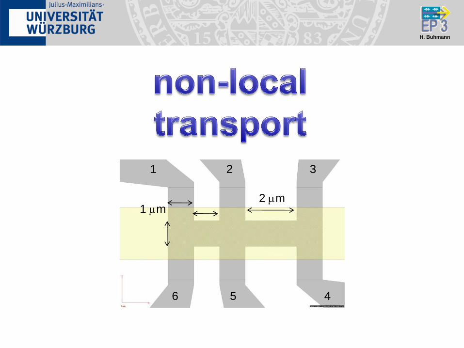
1 mm 2 mm
1 2 3
6 5 4
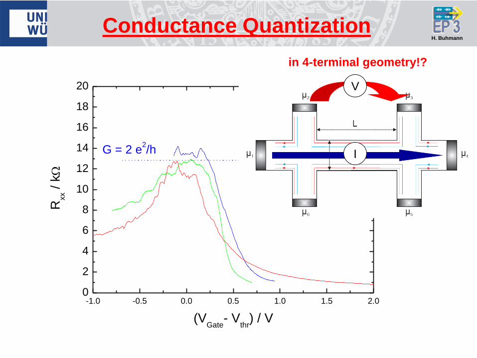
H. Buhmann
-1.0 -0.5 0.0 0.5 1.0 1.5 2.00
2
4
6
8
10
12
14
16
18
20
G = 2 e2/h
Rxx /
k
(VGate
- Vthr
) / V
Conductance Quantization
in 4-terminal geometry!?
V
I

H. Buhmann
Multi-Terminal Probe
-
-
-
-
-
-
210001
121000
012100
001210
000121
100012
T
2
144
3 2
2
142
4 1
2
2
3
t
t
I eG
h
I eG
h
m m
m m
-
-
generally 22
2
)1(
e
hnR t
3
exp4
2 t
t
R
R
h
eG t
2
exp,4 2
Landauer-Büttiker Formalism normal
conducting contacts
no QSHE
--
ij
jijiiiii TRMh
eI mm
2
H. Buhmann
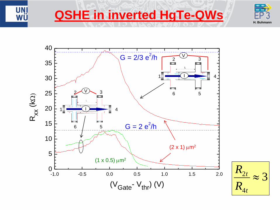
QSHE in inverted HgTe-QWs
34
2 t
t
R
R-1.0 -0.5 0.0 0.5 1.0 1.5 2.0
0
5
10
15
20
25
30
35
40
G = 2/3 e2/h
G = 2 e2/h
Rxx (
k
(VGate- Vthr) (V)
I 1
2 3
4
5 6
V
(1 x 0.5) mm2
(2 x 1) mm2
I 1
2 3
4
5 6
V
H. Buhmann
-5.5 -5.0 -4.5 -4.0 -3.5 -3.0 -2.5 -2.0 -1.5 -1.0 -0.5 0.00
2
4
6
8
10
12
14
16
18
20
22
0
2
4
6
8
10
12
14
@6 mK
Rn
l (k
)I (n
A)
UGate
[ V ]
Q2308-02
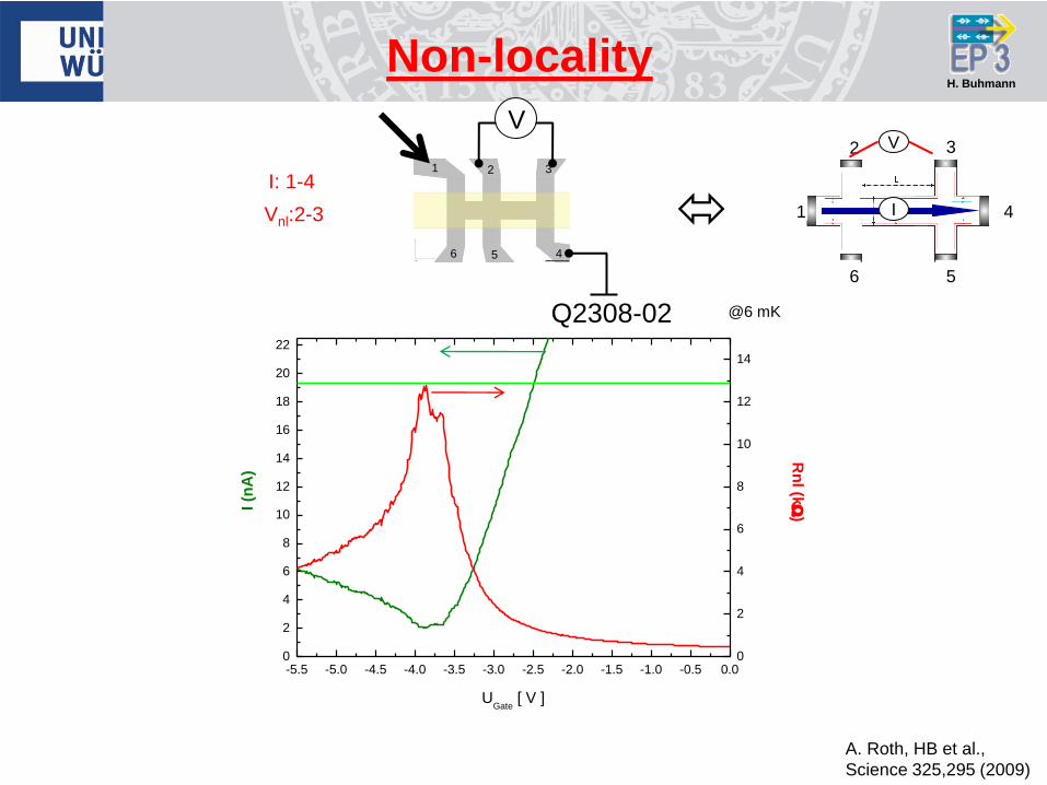
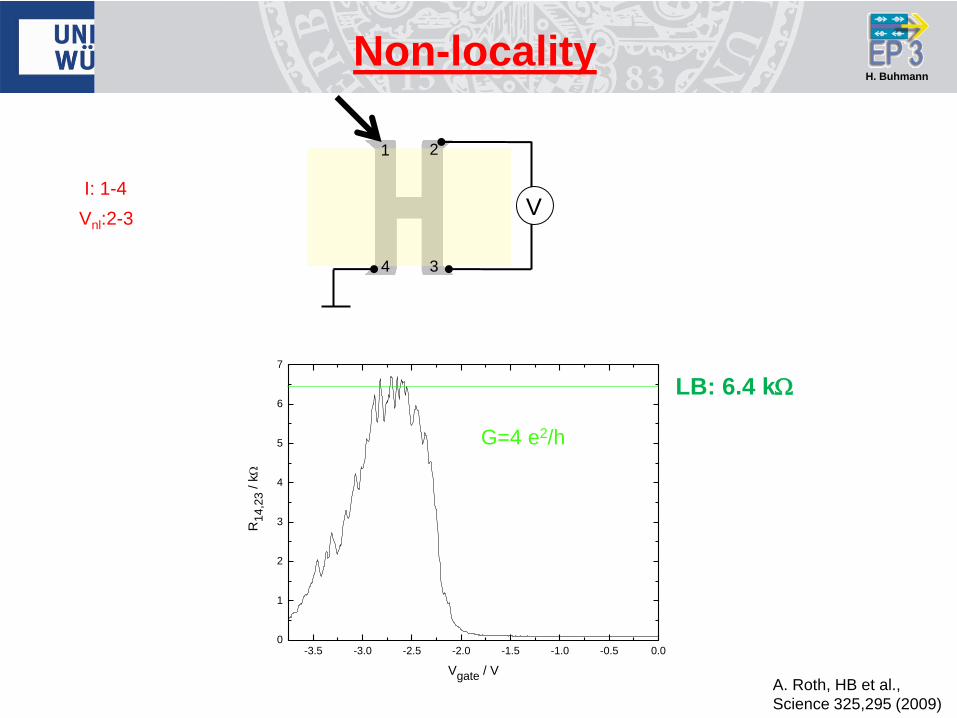
Non-locality
I: 1-4
Vnl:2-3
1 2 3
6 5 4
V
I 1
2 3
4
5 6
V
A. Roth, HB et al.,
Science 325,295 (2009)

H. Buhmann
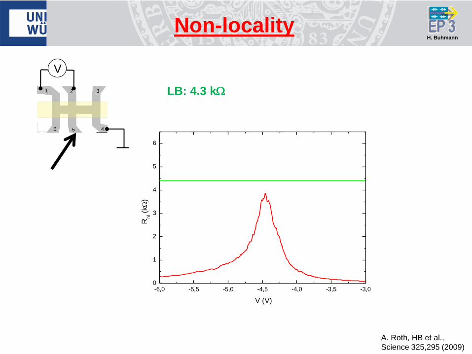
Non-locality
-1 0 1 2 3 40
2
4
6
8
10
12
R (
k
)
V* (V)
G=3 e2/h
I: 1-3
Vnl:5-4
1 2 3
6 5 4
V
4-terminal
LB: 8.6 k
A. Roth, HB et al.,
Science 325,295 (2009)
H. Buhmann
Non-locality
A. Roth, HB et al.,
Science 325,295 (2009)
G=4 e2/h
I: 1-4
Vnl:2-3
1
3
2
4
V
-3.5 -3.0 -2.5 -2.0 -1.5 -1.0 -0.5 0.00
1
2
3
4
5
6
7
R14,2
3 / k
Vgate / V
LB: 6.4 k
H. Buhmann
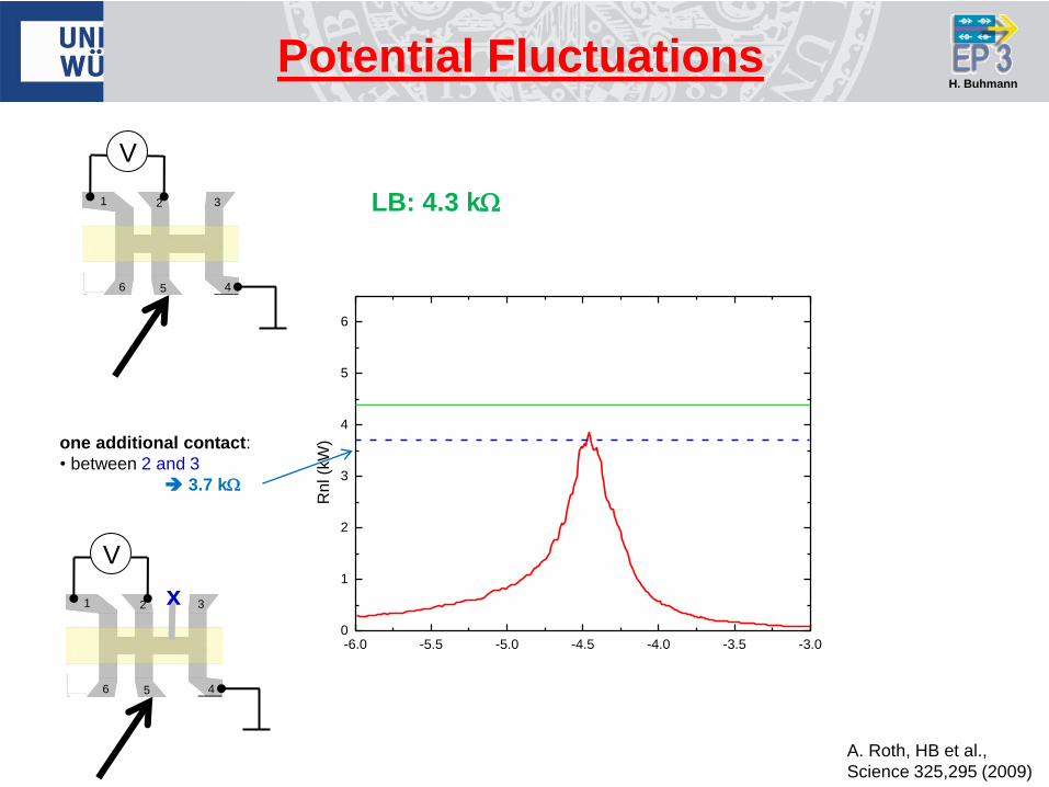
-6,0 -5,5 -5,0 -4,5 -4,0 -3,5 -3,00
1
2
3
4
5
6 R
nl (
k
)
V (V)
LB: 4.3 k
Non-locality
1 2 3
6 5 4
V
A. Roth, HB et al.,
Science 325,295 (2009)
H. Buhmann
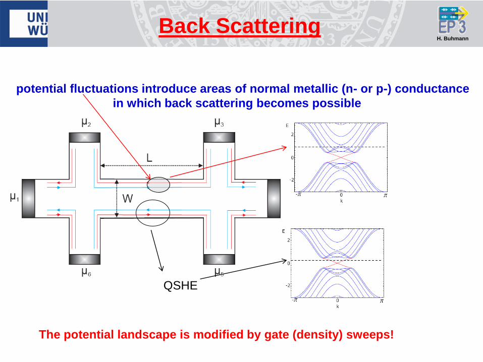
Back Scattering
potential fluctuations introduce areas of normal metallic (n- or p-) conductance
in which back scattering becomes possible
QSHE
The potential landscape is modified by gate (density) sweeps!
H. Buhmann
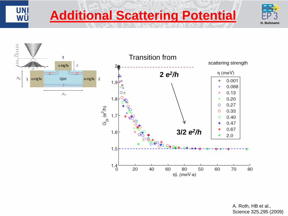
Additional Scattering Potential
A. Roth, HB et al.,
Science 325,295 (2009)
Transition from
2 e2/h
scattering strength
3/2 e2/h
H. Buhmann
-6.0 -5.5 -5.0 -4.5 -4.0 -3.5 -3.00
1
2
3
4
5
6 R
nl (k
W)
LB: 4.3 k
one additional contact:
• between 2 and 3
3.7 k
Potential Fluctuations
1 2 3
6 5 4
V
1 2 3
6 5 4
V
x
A. Roth, HB et al.,
Science 325,295 (2009)
H. Buhmann H. Buhmann
H. Buhmann
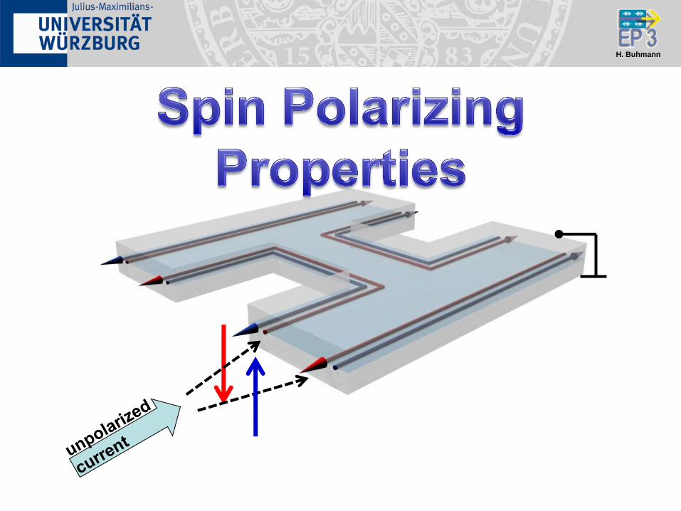
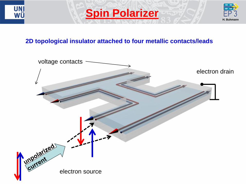
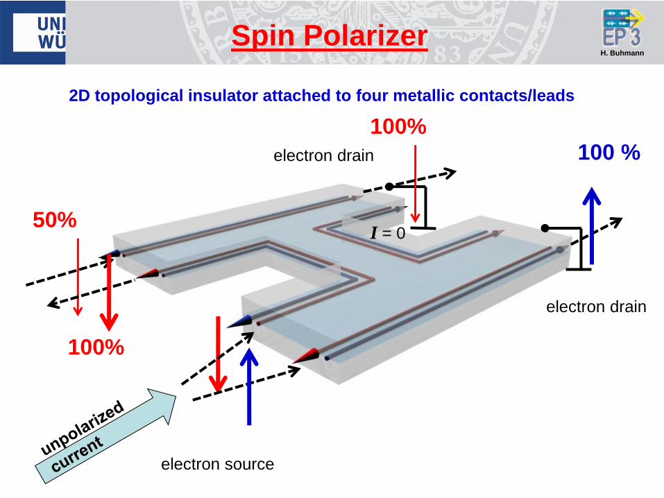
Spin Polarizer
2D topological insulator attached to four metallic contacts/leads
electron drain
voltage contacts
electron source
H. Buhmann
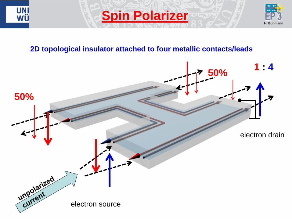
Spin Polarizer
50%
50% 1 : 4
2D topological insulator attached to four metallic contacts/leads
electron drain
electron source
H. Buhmann
Spin Polarizer
50%
100 %
100%
100%
2D topological insulator attached to four metallic contacts/leads
electron drain
electron source
electron drain
I = 0

H. Buhmann
Spin Injector
100 % 100%
spin
injection
even with backscattering!
2D topological insulator attached to four metallic contacts/leads
H. Buhmann
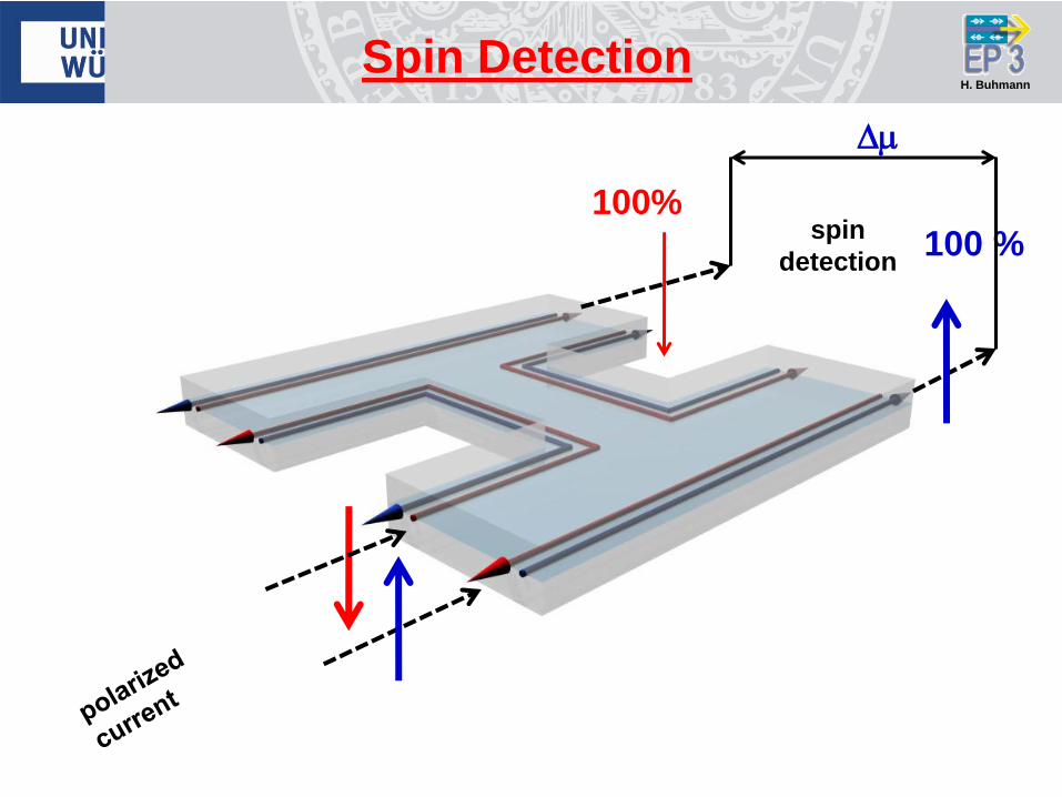
Spin Detection
100 % 100%
spin
detection
Dm
H. Buhmann
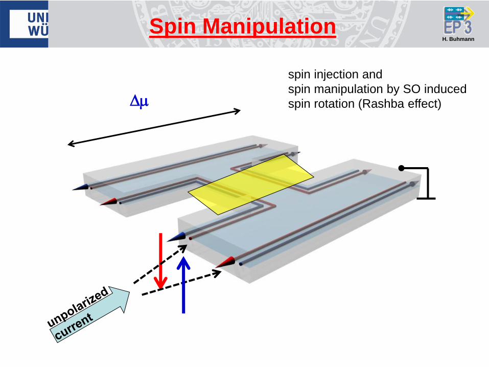
Spin Manipulation
Dm
spin injection and
spin manipulation by SO induced
spin rotation (Rashba effect)
H. Buhmann H. Buhmann
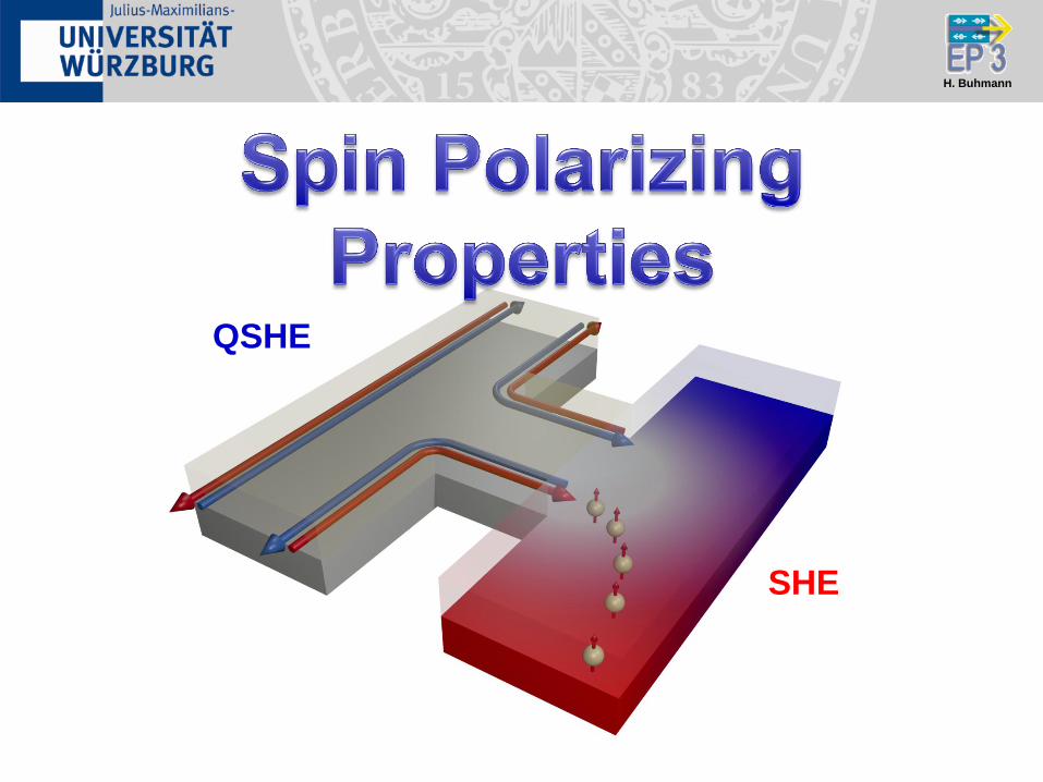
QSHE
SHE
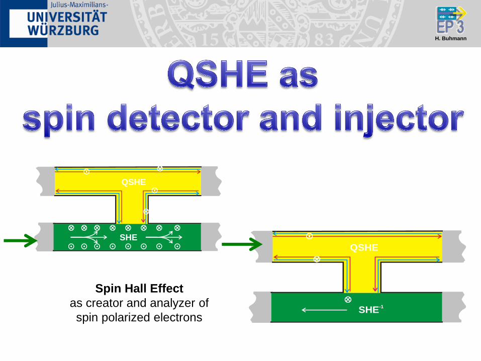
H. Buhmann H. Buhmann
SHE-1
QSHE
Spin Hall Effect
as creator and analyzer of
spin polarized electrons
SHE
QSHE
H. Buhmann
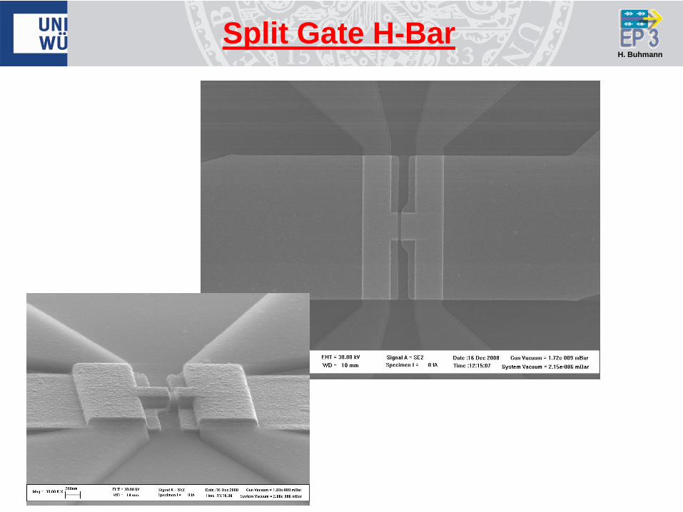
Split Gate H-Bar
H. Buhmann
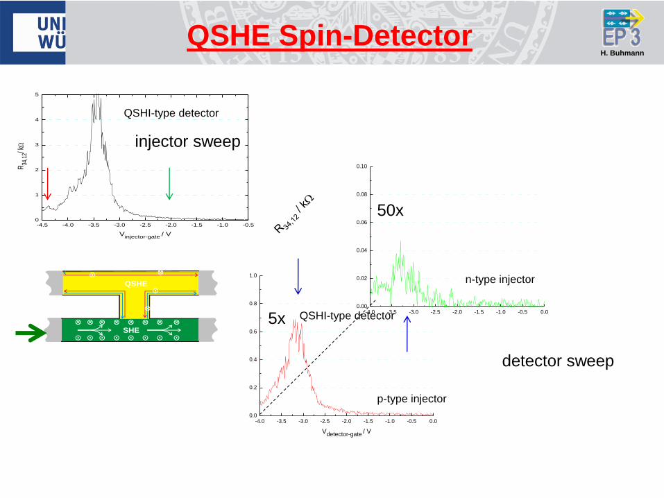
QSHE Spin-Detector
-4.0 -3.5 -3.0 -2.5 -2.0 -1.5 -1.0 -0.5 0.00.00
0.02
0.04
0.06
0.08
0.10
-4.0 -3.5 -3.0 -2.5 -2.0 -1.5 -1.0 -0.5 0.00.0
0.2
0.4
0.6
0.8
1.0
Vdetector-gate / V
5x
50x
n-type injector
p-type injector
SHE
QSHE
QSHI-type detector
-4.5 -4.0 -3.5 -3.0 -2.5 -2.0 -1.5 -1.0 -0.50
1
2
3
4
5
R34
,12/ k
Vinjector-gate
/ V
QSHI-type detector
injector sweep
detector sweep
H. Buhmann
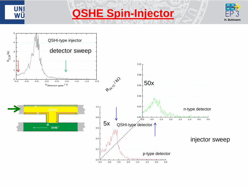
QSHE Spin-Injector
5x
50x
n-type detector
p-type detector
-3.5 -3.0 -2.5 -2.0 -1.5 -1.0 -0.5 0.00.00
0.02
0.04
0.06
0.08
0.10
-3.5 -3.0 -2.5 -2.0 -1.5 -1.0 -0.5 0.00.0
0.2
0.4
0.6
0.8
1.0
SHE-1
QSHE
QSHI-type detector
-4.5 -4.0 -3.5 -3.0 -2.5 -2.0 -1.5 -1.0 -0.50
1
2
3
4
5
R12
,34/ k
Vdetector-gate / V
QSHI-type injector
detector sweep
injector sweep

H. Buhmann H. Buhmann
C. Brüne et al., Nature Physics, 8, 485 (2012)
H. Buhmann
V
-3.5 -3.0 -2.5 -2.0 -1.5 -1.0 -0.5 0.00
20
40
60
80
100
Rn
on
loc/
Ugate
/ V
-3.5 -3.0 -2.5 -2.0 -1.5 -1.0 -0.5 0.00
200
400
600
800
1000
Rn
on
loc/
Ugate
/ V
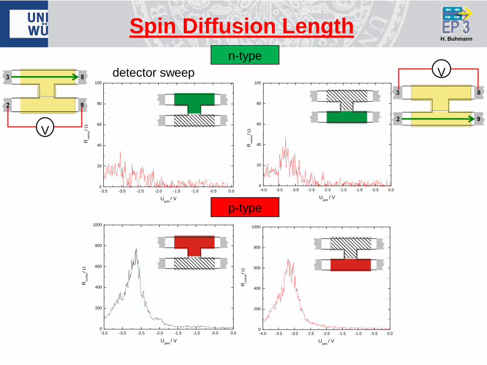
detector sweep
p-type
n-type
V
-4.0 -3.5 -3.0 -2.5 -2.0 -1.5 -1.0 -0.5 0.00
200
400
600
800
1000
Rn
on
loc/
Ugate
/ V
-4.0 -3.5 -3.0 -2.5 -2.0 -1.5 -1.0 -0.5 0.00
20
40
60
80
100
Rn
on
loc/
Ugate
/ V
Spin Diffusion Length
H. Buhmann H. Buhmann

H. Buhmann H. Buhmann
2d Dirac system
• hybridization of the top and bottom surface lead to a gapped
states on these two surfaces
• free 1d Dirac electrons at the edges of the layer
H. Buhmann H. Buhmann
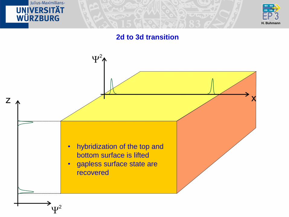
2d to 3d transition
• hybridization of the top and
bottom surface is lifted
• gapless surface state are
recovered
H. Buhmann H. Buhmann
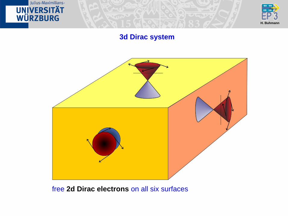
3d Dirac system
free 2d Dirac electrons on all six surfaces
H. Buhmann H. Buhmann

H. Buhmann
-0.3 -0.2 -0.1 0.0 0.1 0.2 0.3
-400
-300
-200
-100
0
100
EF
E, m
eV
k, nm-1
Bulk HgTe
x-ray diffraction (115 reflex)
fully strained
70 nm HgTe
on CdTe substrate
Band Structure
- gap openning (10…20 meV)
- two Dirac cones on
different surfaces
L1
H1
E1
5.1 5.2 5.3 5.4 5.5 5.6 5.7 5.8 5.9 6.0 6.1 6.2 6.3 6.4 6.5 6.76.6
1.0
1.5
0.5
0.0
-0.5
2.0
2.5
3.0
3.5
4.0
4.5
5.0
6.0
5.5
Bandgap vs. lattice constant(at room temperature in zinc blende structure)
Ban
dga
p e
ner
gy
(eV
)
lattice constant a [Å]0© CT-CREW 1999

H. Buhmann
0 2 4 6 8 10 12 14 160
2000
4000
6000
8000
10000
12000
14000
16000
0
2000
4000
6000
8000
10000
12000
14000
Rxx
(SdH)
Rxx in O
hm
B in Tesla
n=4
n=3
Rxy
(Hall)
Rxy in O
hm
n=2
QHE in a 3D TI system

H. Buhmann
2 4 6 8 10 12 14 160
2
4
6
8
10
12
14
s
xy [e
2/h
]
B [T]
0 2 4 6 8 10 12 14 160
2
4
6
8
10
12
14
16
0
2
4
6
8
10
12
14
Rxx [k
]
B [T]
Rxy [k
]
Brüne et al., Phys. Rev. Lett. 106, 126803 (2011)
QHE in a 3D TI system
h
enxy
2
2
1
s
single Dirac
surface
H. Buhmann
2 4 6 8 10 12 14 160
2000
4000
6000
8000
10000
Rxx in
Oh
m
B in Tesla
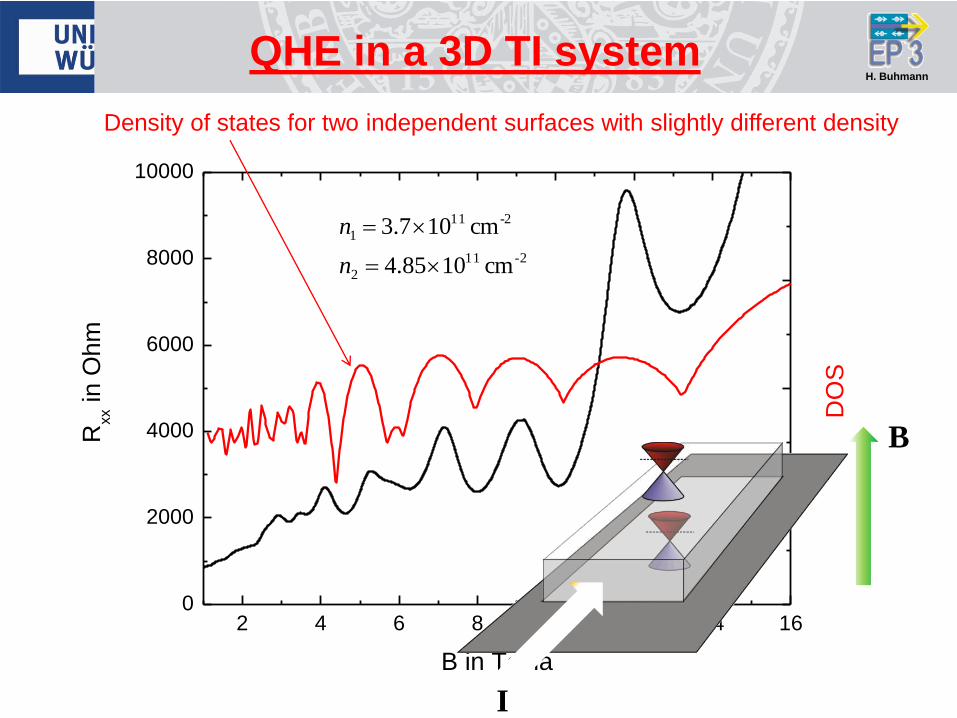
DO
S
Density of states for two independent surfaces with slightly different density
2-11
2
-211
1
cm 1085.4
cm 107.3
n
n
QHE in a 3D TI system
B
I

H. Buhmann
Brüne et al., Phys. Rev. Lett. 106, 126803 (2011)
QHE in a 3D TI system
H. Buhmann
QHE in a 3D TI system
0 2 4 6 8 10 12 14 16
-1
0
1
2
3
4
5 0
5
10
15
20
25
Vgate [V
]
B [T]
Rx
y [
k
]
Rxy from -1 V to 5 V n = 1
n = 3
n = 5
flat band condition at -1 V top and bottom surface exhibit approx. the same
carrier density.
h
enxy
2
12 s for ntop = nbottom
H. Buhmann
0 2 4 6 8 10 12 14 16
-1
0
1
2
3
4
5 0
5
10
15
20
25
Vgate [V
]
B [T]
Rx
y [
k
]
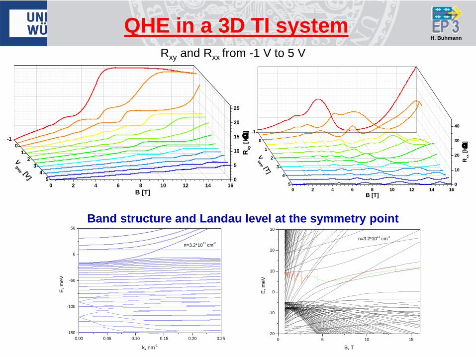
QHE in a 3D TI system Rxy and Rxx from -1 V to 5 V
0 2 4 6 8 10 12 14 16
-1
0
1
2
3
4
5 0
10
20
30
40
Vgate [T
]
B [T]
Rx
x [
k
]
0 5 10 15
-20
-10
0
10
20
30
n=3.2*1011
cm-2
E, m
eV
B, T
0.00 0.05 0.10 0.15 0.20 0.25
-150
-100
-50
0
50
n=3.2*1011
cm-2
E, m
eV
k, nm-1
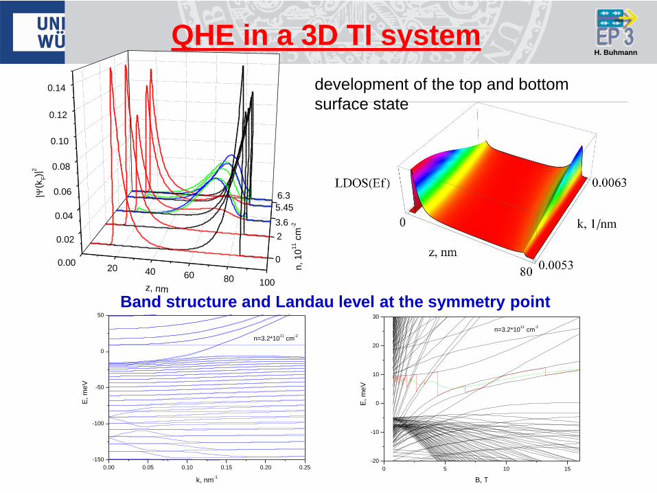
Band structure and Landau level at the symmetry point
H. Buhmann
QHE in a 3D TI system
0 5 10 15
-20
-10
0
10
20
30
n=3.2*1011
cm-2
E, m
eV
B, T
0.00 0.05 0.10 0.15 0.20 0.25
-150
-100
-50
0
50
n=3.2*1011
cm-2
E, m
eV
k, nm-1
Band structure and Landau level at the symmetry point
20 40 60 80 100
0.00
0.02
0.04
0.06
0.08
0.10
0.12
0.14
6.3
5.45
3.6
2
0
|(k
F)|
2
n, 10
11 c
m-2
z, nm
development of the top and bottom
surface state
H. Buhmann H. Buhmann
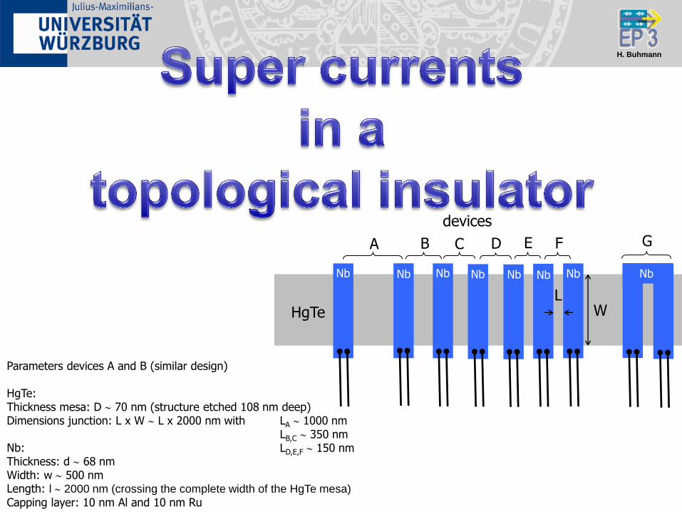
Parameters devices A and B (similar design) HgTe: Thickness mesa: D 70 nm (structure etched 108 nm deep) Dimensions junction: L x W L x 2000 nm with LA 1000 nm LB,C 350 nm LD,E,F 150 nm
HgTe
E F
devices
L W
D C B A
Nb: Thickness: d 68 nm Width: w 500 nm Length: l 2000 nm (crossing the complete width of the HgTe mesa) Capping layer: 10 nm Al and 10 nm Ru
Nb Nb Nb Nb Nb Nb Nb Nb
G
H. Buhmann
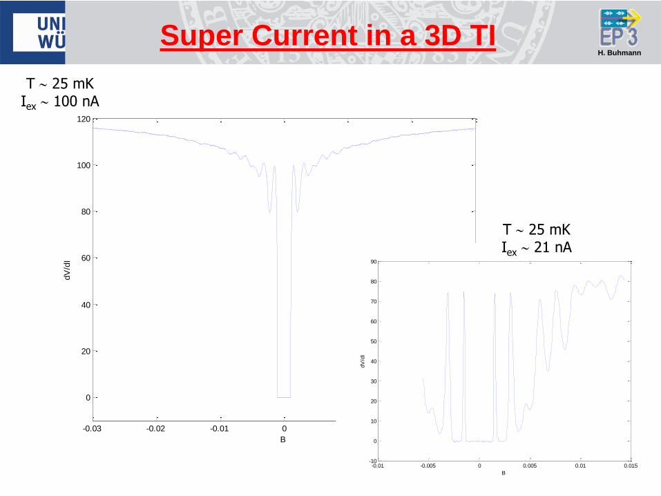
-0.03 -0.02 -0.01 0 0.01 0.02 0.03
0
20
40
60
80
100
120dV/dI(B)
B
dV
/dI
T 25 mK Iex 100 nA
Super Current in a 3D TI
-0.01 -0.005 0 0.005 0.01 0.015-10
0
10
20
30
40
50
60
70
80
90dV/dI(B) T = 25 mK
B
dV
/dI
T 25 mK Iex 21 nA

H. Buhmann
Summary
observation in 2D systems
– quantum spin Hall effect
• spin polarized quantized edge channel transport
observation in 3D systems
– quantum Hall effect of two Dirac surfaces
– proximity induced super conductivity
H. Buhmann
Acknowledgements
Quantum Transport Group (Würzburg, H. Buhmann)
C. Brüne
C. Ames
P. Leubner
L. Maier
M. Mühlbauer
C. Thienel
J. Mutterer
D. Knott
A. Astakhova
Ex-QT: C.R. Becker
T. Beringer
M. Lebrecht
J. Schneider
S. Wiedmann
N. Eikenberg
R. Rommel
F. Gerhard
B. Krefft
A. Roth
B. Büttner
R. Pfeuffer
R. Schaller
Stanford University
S.-C. Zhang
X.L. Qi
(J. Maciejko)
(T. L. Hughes)
M. König
Texas A&M University
J. Sinova
Lehrstuhl für Experimentelle Physik 3: L.W. Molenkamp
Univ. Würzburg
Inst. f. Theoretische Physik
E.M. Hankiewicz
B. Trautzettel
Collaborations:
Penn. State University
CX. Liu

H. Buhmann H. Buhmann
Quantum Spin Hall Effekt
Science 318, 766 (2007)
The Quantum Spin Hall Effect:
Theory and Experiment
J. Phys. Soc. Jap.
Vol. 77, 31007 (2008) Intrinsic Spin Hall Effekt
Nature Physics 6, 448 (2010)
Nonlocal edge state transport
in the quantum spin Hall state
Science 325, 294 (2009)
Quantum Hall Effect from the
Topological Surface States of
Strained Bulk HgTe
Phys. Rev. Lett. 106, 126803 (2011)
Spin polarization of the quantum
spin Hall edge states
Nature Physics, 8,485 (2012)


![ˇ ˆ ˙ · 3. Buhmann, M.D. Radial Basis Function: Theory and Implementations [] / M.D. Buhmann. – Cambridge Monographs on Applied and Computational Mathematics, 2003. 4. fast](https://img.pdfslide.us/doc/110x75/5ecd0e0bba2cd96faa6777f8/-3-buhmann-md-radial-basis-function-theory-and-implementations-.jpg)


![[John Heil, Alfred Mele] Mental Causation](https://img.pdfslide.us/doc/110x75/55cf9a9f550346d033a29fa7/john-heil-alfred-mele-mental-causation.jpg)