Embed Size (px)
Citation preview

12
Hardware Design of Embedded Systems for Security Applications
Camel Tanougast, Abbas Dandache, Mohamed Salah Azzaz and Said Sadoudi
University Lorraine of Metz France
1. Introduction
Embedded systems are electronic computer systems designed for dedicated operating functions, often while respecting several constraints like real-time computing, power consumption, size and cost, etc. Embedded systems control many devices in common use today such as smartphones, GPS, codec GSM, decoders, MP3, MPEG62, MPEG4, PDAs, RFIDs, smart cards and networked sensors etc. Generally, they are controlled by one or more main processing cores that are typically either Microcontrollers, Digital Signal Processors (DSPs) or Field Programmable Gate Arrays (FPGAs). These systems are embedded as part of a complete electronic system, often including software, hardware, and communication and sensor parts. By contrast, a general-purpose computer - such as a Personal Computer (PC) - is designed to be flexible and to meet a wide range of end-user needs. The key characteristic of an embedded system is that it is dedicated to the handling of a particular task. They may require very powerful processors and extensive communications. Ideally, these embedded systems are completely self-contained and will typically run off a battery source for many years before the batteries need to be changed or charged. Since such systems are embedded and dedicated to specific tasks, design engineers search to optimise them by reducing their size (miniaturisation made possible by advanced IC design in order to couple full communication subsystems to sophisticated sensors) and cost in terms of energy consumption, memory and logic resources, while increasing their reliability and performance. Consequently, embedded systems are especially suited for use in transportation, medical applications, safety and security. Indeed, in dealing with security, embedded systems can be self-sufficient and should be able to deal with communication systems. Considering these specific conditions, in the fields of information and communication technology, embedded systems designers are faced with many challenges in terms of both the trade-off between cost/performance/power and architecture design. This is especially true for embedded systems designs, which often operate in non-secure environments, while at the same time being constrained by such factors as computational capacity, memory size and - in particular - power consumption. One challenge is in the design of hardware architecture able to meet the appropriate level of security and – consequently – the best trade-off between hardware resources and the best throughput rates for real-time embedded applications.
A digital implementation of chaotic generators presents certain advantages and provides accuracy and a significant hope for integration in embedded applications, especially for data
www.intechopen.com
Embedded Systems – High Performance Systems, Applications and Projects
234
encryption and secure communications between embedded systems. Unlike analogue implementations, which exhibit various practical difficulties in ensuring information recovery and dealing with the problem of chaotic synchronisation (since the component values vary with age and temperature, etc.), a digital implementation avoids the parameter mismatch between transmitter and receiver. Indeed, a programmable hardware fabric like a FPGA (Field Programmable Logic Array) is taking an increasingly important place in the design of embedded digital systems. This is due to the excellent trade-off between computational power and the flexibility of processing which it provides.
This chapter is organised as follows: In Section 2, the related embedded design approaches suitable for embedded secure application (encryption) are briefly described. Section 3 explores the architecture of a hardware implementation for helping system designers who are faced with many challenges with regards to the trade-off between cost/performance/power/security and architecture design. Section 4 gives an overview, namely a characterisation of three dimensional (3-D) continuous chaotic systems used for embedded encryption applications. In this section, the background of the digital design based on a numerical resolution method of the 3D chaotic systems is given. Section 5 presents and discusses in detail the various steps involved in the design of a chaotic system as well as the design of its programmable hardware technology, and it illustrates this with the Genesio's chaotic system designed in a FPGA. Finally, Section 6 summarises and concludes the chapter.
2. Overview of the hardware design of embedded systems
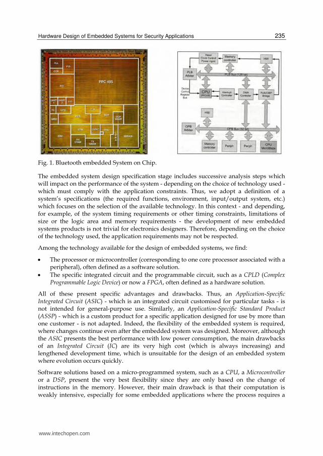
The electronic computing architecture of embedded systems is often composed of embedded blocks as parts of a complete device, often including hardware, an interface and mechanical parts. Usually, these systems are designed digitally in order to be flexible and to meet a wide range of application constraints. Therefore, embedded systems contain processing cores (CPUs) associated with several peripherals (integrated peripherals like Analogue-to-Digital Converters (ADCs), Digital-to-Analogue Converters (DACs), analogue signal conditioning blocks allowing them to operate as a System-on-Chip) that typically consist of Microcontrollers, Digital Signal Processors (DSPs) or else hardware specific cores tailored for dedicated tasks. These embedded architectures allow a good trade-off between performance, cost and application constraints (real-time processing, power consumption, etc.). Usually, these embedded systems are defined as Systems on Chip (SoC) and presented in a hand-format. Figure 1 provides an overview of one embedded System on Chip (a Bluetooth System on Chip).
However, the significant requirements and different constraints for an embedded application and the characteristics of the embedded system dedicated to handling a particular task must be taken into account. Their requirements often lead to the design of a specific embedded system for application in just one field. In this context, a methodological approach based on embedded design flow and available technologies must be considered by taking into account the advantages and main drawbacks for meeting the application constraints of the embedded application under consideration. Since embedded systems are dedicated to certain specific tasks, design engineers can optimise them in order to reduce their size and their cost, as well as increasing their reliability and performance by considering the following hardware design approach.
www.intechopen.com
Hardware Design of Embedded Systems for Security Applications
235
Fig. 1. Bluetooth embedded System on Chip.
The embedded system design specification stage includes successive analysis steps which will impact on the performance of the system - depending on the choice of technology used - which must comply with the application constraints. Thus, we adopt a definition of a system’s specifications (the required functions, environment, input/output system, etc.) which focuses on the selection of the available technology. In this context - and depending, for example, of the system timing requirements or other timing constraints, limitations of size or the logic area and memory requirements - the development of new embedded systems products is not trivial for electronics designers. Therefore, depending on the choice of the technology used, the application requirements may not be respected.
Among the technology available for the design of embedded systems, we find:
The processor or microcontroller (corresponding to one core processor associated with a peripheral), often defined as a software solution.
The specific integrated circuit and the programmable circuit, such as a CPLD (Complex Programmable Logic Device) or now a FPGA, often defined as a hardware solution.
All of these present specific advantages and drawbacks. Thus, an Application-Specific Integrated Circuit (ASIC) - which is an integrated circuit customised for particular tasks - is not intended for general-purpose use. Similarly, an Application-Specific Standard Product (ASSP) - which is a custom product for a specific application designed for use by more than one customer - is not adapted. Indeed, the flexibility of the embedded system is required, where changes continue even after the embedded system was designed. Moreover, although the ASIC presents the best performance with low power consumption, the main drawbacks of an Integrated Circuit (IC) are its very high cost (which is always increasing) and lengthened development time, which is unsuitable for the design of an embedded system where evolution occurs quickly.
Software solutions based on a micro-programmed system, such as a CPU, a Microcontroller or a DSP, present the very best flexibility since they are only based on the change of instructions in the memory. However, their main drawback is that their computation is weakly intensive, especially for some embedded applications where the process requires a
www.intechopen.com
Embedded Systems – High Performance Systems, Applications and Projects
236
long computation time. Therefore, for most applications the computation time will be prohibitive if a software solution is adopted. This effect is directly related to the nature of Von Neumann's architecture of a CPU which cannot operate in a parallel fashion.
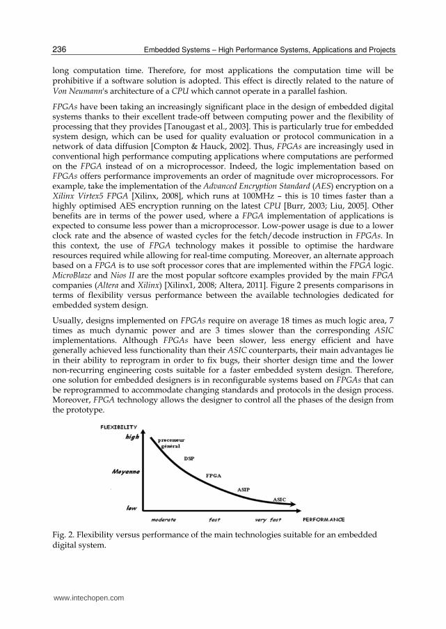
FPGAs have been taking an increasingly significant place in the design of embedded digital systems thanks to their excellent trade-off between computing power and the flexibility of processing that they provides [Tanougast et al., 2003]. This is particularly true for embedded system design, which can be used for quality evaluation or protocol communication in a network of data diffusion [Compton & Hauck, 2002]. Thus, FPGAs are increasingly used in conventional high performance computing applications where computations are performed on the FPGA instead of on a microprocessor. Indeed, the logic implementation based on FPGAs offers performance improvements an order of magnitude over microprocessors. For example, take the implementation of the Advanced Encryption Standard (AES) encryption on a Xilinx Virtex5 FPGA [Xilinx, 2008], which runs at 100MHz – this is 10 times faster than a highly optimised AES encryption running on the latest CPU [Burr, 2003; Liu, 2005]. Other benefits are in terms of the power used, where a FPGA implementation of applications is expected to consume less power than a microprocessor. Low-power usage is due to a lower clock rate and the absence of wasted cycles for the fetch/decode instruction in FPGAs. In this context, the use of FPGA technology makes it possible to optimise the hardware resources required while allowing for real-time computing. Moreover, an alternate approach based on a FPGA is to use soft processor cores that are implemented within the FPGA logic. MicroBlaze and Nios II are the most popular softcore examples provided by the main FPGA companies (Altera and Xilinx) [Xilinx1, 2008; Altera, 2011]. Figure 2 presents comparisons in terms of flexibility versus performance between the available technologies dedicated for embedded system design.
Usually, designs implemented on FPGAs require on average 18 times as much logic area, 7 times as much dynamic power and are 3 times slower than the corresponding ASIC implementations. Although FPGAs have been slower, less energy efficient and have generally achieved less functionality than their ASIC counterparts, their main advantages lie in their ability to reprogram in order to fix bugs, their shorter design time and the lower non-recurring engineering costs suitable for a faster embedded system design. Therefore, one solution for embedded designers is in reconfigurable systems based on FPGAs that can be reprogrammed to accommodate changing standards and protocols in the design process. Moreover, FPGA technology allows the designer to control all the phases of the design from the prototype.
Fig. 2. Flexibility versus performance of the main technologies suitable for an embedded digital system.
www.intechopen.com
Hardware Design of Embedded Systems for Security Applications
237
A recent trend has been to take a coarse-grained architectural approach by combining the logic blocks and interconnections of traditional FPGAs with embedded microprocessors and related peripherals. The goal is to form a complete "System on a Programmable Chip" suitable for a large performing embedded system. In this context, advances in Very-large-Scale Integration (VLSI) technology have been employed to the manufacturing of reconfigurable logic for FPGA chips; and helped with their rapid growth in logic capacity, performance and popularity. In summary, a FPGA-based architecture is suitable for efficient computing of embedded applications with high data rate to compute. It is an excellent alternative to performing fast processing in order to reduce the total processing time, while maintaining a good level of flexibility in allowing any modifications in the run time required for current embedded systems.
3. Architecture exploration
The objective of an architecture exploration is to find an efficient matching between an algorithm and the architecture. The aim is to realise an optimal implementation that satisfies the various constraints (real-time, logic area, etc.). Therefore, digital hardware techniques can be used to implement efficiency in embedded applications like chaotic generators for embedded encryption by using digital devices such as microcontrollers, DSPs, ASICs, processors and FPGA technologies. The choice of implementation in a digital system is driven by many criteria and is heavily dependent on the application area. Table 1 gives the main contrasting features of current digital technologies for the design of embedded systems.
Features
Processors / DSP / Microcontroller (Software)
FPGA (Hardware programmable)
ASICs (Hardware)
Silicon area Fixed Variable Fixed and low
Speed Moderate Fast Very fast
Consumption Moderate High Weak
Cost Low Moderate High
Prototyping Yes Yes No
Table 1. Features of the main technologies available for the design of embedded systems.
As mentioned previously, the designer can realise any embedded system (based on either the logic design and/or software design thanks to the embedded softcore processor) by utilising programmable logic devices in the form of FPGAs and CPLDs [Brown & Rose, 1996]. In the design context, the objective of Algorithm/Architecture Adequation (architecture exploration based on A3 methodology [Sorel, 1994]) is to realise an optimal implementation which satisfies the constraints (real-time, logic area, etc.). In this Section, we illustrate an analysis of the costs and benefits of the use of reconfigurable technology such as FPGAs.
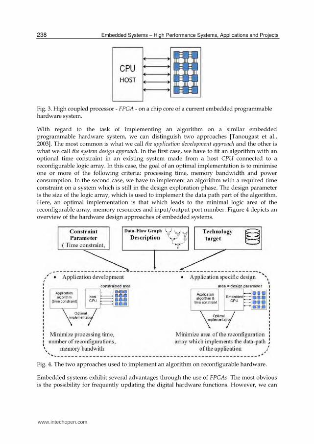
In practice, the actual embedded system is composed inside the chip of a high coupled
processor with a Programmable Array (FPGA, CPLD, etc). Indeed, such a hardware structure
allows the combination of the advantages of these two technologies inside the same circuit.
Consequently, coupling can reduce the main drawbacks of these technologies when they are
used individually. Figure 3 illustrated one such embedded programmable hardware core
which is usually associated with peripheral modules.
www.intechopen.com
Embedded Systems – High Performance Systems, Applications and Projects
238
Fig. 3. High coupled processor - FPGA - on a chip core of a current embedded programmable hardware system.
With regard to the task of implementing an algorithm on a similar embedded programmable hardware system, we can distinguish two approaches [Tanougast et al., 2003]. The most common is what we call the application development approach and the other is what we call the system design approach. In the first case, we have to fit an algorithm with an optional time constraint in an existing system made from a host CPU connected to a reconfigurable logic array. In this case, the goal of an optimal implementation is to minimise one or more of the following criteria: processing time, memory bandwidth and power consumption. In the second case, we have to implement an algorithm with a required time constraint on a system which is still in the design exploration phase. The design parameter is the size of the logic array, which is used to implement the data path part of the algorithm. Here, an optimal implementation is that which leads to the minimal logic area of the reconfigurable array, memory resources and input/output port number. Figure 4 depicts an overview of the hardware design approaches of embedded systems.
Fig. 4. The two approaches used to implement an algorithm on reconfigurable hardware.
Embedded systems exhibit several advantages through the use of FPGAs. The most obvious is the possibility for frequently updating the digital hardware functions. However, we can
www.intechopen.com
Hardware Design of Embedded Systems for Security Applications
239
also use the dynamic resources allocation feature in order to instantiate each operator for the strict required time. This permits the enhancement of silicon efficiency by reducing the reconfigurable array’s area. Consequently, the goal of the embedded system designers in architectural design flow is to minimise the FPGA resources needed for the implementation of a time constrained algorithm. So, the challenge is twofold. Firstly, to find a trade-off between flexibility and algorithm implementation efficiency through the programmable logic-array coupled with a CPU host (processor, DSP, etc.). Secondly, to obtain an optimal architecture synthesis allowing the best hardware implementation trade-off required for embedded applications.
In the rest of this chapter, we describe the main steps in the hardware design of embedded systems for security applications. We will consider an encryption process based on key chaotic generators and a mechanism for mixing the key with plaintext (encryption/decryption process).
4. Embedded digital chaotic cryptosystem
Chaos-based encryption suggests a new and efficient way of dealing with the problem of fast and highly secure data encryption. To implement the chaotic behaviour generators and the chaotic attractors associated with certain practical applications, many methods based on analogue circuits are used, such as switched capacitors or analogue Complementary Metal Oxide Semiconductor (CMOS) technology [Matsumoto, 1987; Giannakopoulos et al., 2007; Ozoguz et al., 2005; Cha & Lee, 2005]. However, these methods exhibit some practical difficulties since the component values vary with age and temperature, etc. [Aseeri et al., 2002; Sobhy et al., 1999]. To overcome this problem, a digital implementation of chaotic generators can be used, since the problem of parameter mismatch does not exist and it provides accuracy and a significant possibility of integration in the embedded system, allowing many possibilities for embedded applications. The originality of this cipher scheme is that it allows for low cost data encryption for embedded systems while still providing a good trade-off between performance and hardware resources. The experimental results have demonstrated the feasibility and efficiency of this secure solution for FPGA technology. In the rest of this chapter, thorough experimental tests are presented with detailed analysis, demonstrating the high security and fast encryption speed suitable for embedded cryptosystems where resource optimisation is required in the field of embedded applications.
4.1 Chaotic generators-based encryption
In recent years, a variety of encryption schemes have been proposed for real-time secure data transmission over the Internet and through wireless networks by embedded systems. Among them, chaos-based algorithms have shown some attractive properties in terms of security, complexity, speed, computing power and computational overheads, etc. More precisely, although chaotic systems are characterised by specific attractors, their generated chaotic signals are non-periodic, uncorrelated and appear random in the time domain. These properties increase the complexity of a cryptanalysis attack in terms of the visualisation and identification of the signals used for key generation through a key space analysis. Hence, embedded cryptosystems for secure communications based on chaos theory have been proposed and developed while showing that these embedded systems can be controlled
www.intechopen.com
Embedded Systems – High Performance Systems, Applications and Projects
240
[Lorenz, 1963; Yang, 2004]. Indeed, the synchronisation between two identical chaotic embedded systems corresponding to the data encryption transmission module and the decryption reception module has been reported [Carroll & Pecora, 1990]. Consequently, it was concluded that a key generator based on chaos theory could be useful with regard to secure communication systems because chaos is extremely sensitive to initial conditions and parameters [Azzaz et al., 2011].
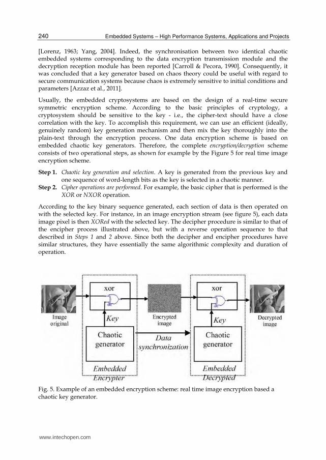
Usually, the embedded cryptosystems are based on the design of a real-time secure symmetric encryption scheme. According to the basic principles of cryptology, a cryptosystem should be sensitive to the key - i.e., the cipher-text should have a close correlation with the key. To accomplish this requirement, we can use an efficient (ideally, genuinely random) key generation mechanism and then mix the key thoroughly into the plain-text through the encryption process. One data encryption scheme is based on embedded chaotic key generators. Therefore, the complete encryption/decryption scheme consists of two operational steps, as shown for example by the Figure 5 for real time image encryption scheme.
Step 1. Chaotic key generation and selection. A key is generated from the previous key and one sequence of word-length bits as the key is selected in a chaotic manner.
Step 2. Cipher operations are performed. For example, the basic cipher that is performed is the XOR or NXOR operation.
According to the key binary sequence generated, each section of data is then operated on with the selected key. For instance, in an image encryption stream (see figure 5), each data image pixel is then XORed with the selected key. The decipher procedure is similar to that of the encipher process illustrated above, but with a reverse operation sequence to that described in Steps 1 and 2 above. Since both the decipher and encipher procedures have similar structures, they have essentially the same algorithmic complexity and duration of operation.
Fig. 5. Example of an embedded encryption scheme: real time image encryption based a chaotic key generator.
www.intechopen.com
Hardware Design of Embedded Systems for Security Applications
241
4.2 Tri-dimensional chaotic systems: chaos behavioural modelling and software simulation
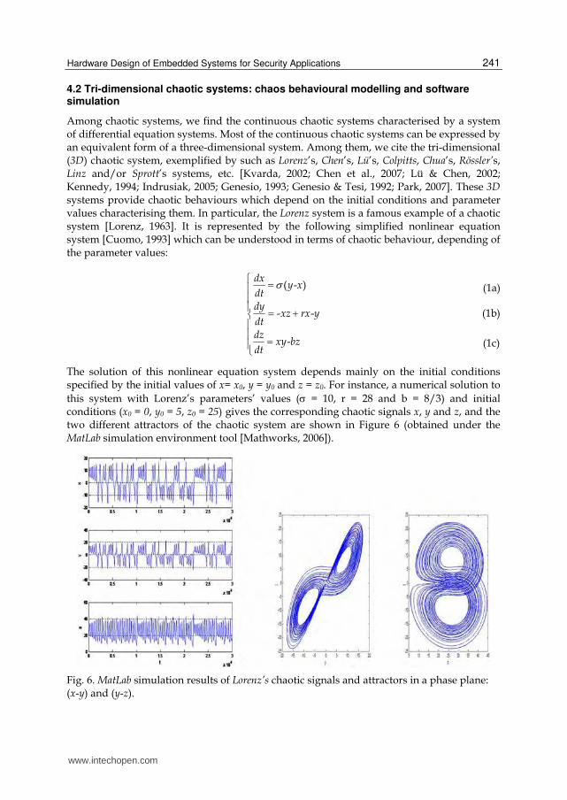
Among chaotic systems, we find the continuous chaotic systems characterised by a system of differential equation systems. Most of the continuous chaotic systems can be expressed by an equivalent form of a three-dimensional system. Among them, we cite the tri-dimensional (3D) chaotic system, exemplified by such as Lorenz’s, Chen’s, Lü’s, Colpitts, Chua’s, Rössler’s, Linz and/or Sprott’s systems, etc. [Kvarda, 2002; Chen et al., 2007; Lü & Chen, 2002; Kennedy, 1994; Indrusiak, 2005; Genesio, 1993; Genesio & Tesi, 1992; Park, 2007]. These 3D systems provide chaotic behaviours which depend on the initial conditions and parameter values characterising them. In particular, the Lorenz system is a famous example of a chaotic system [Lorenz, 1963]. It is represented by the following simplified nonlinear equation system [Cuomo, 1993] which can be understood in terms of chaotic behaviour, depending of the parameter values:
( - )
- -
-
dxy x
dtdy
xz rx ydtdz
xy bzdt
(1b)
The solution of this nonlinear equation system depends mainly on the initial conditions specified by the initial values of x= x0, y = y0 and z = z0. For instance, a numerical solution to
this system with Lorenz’s parameters’ values ( = 10, r = 28 and b = 8/3) and initial conditions (x0 = 0, y0 = 5, z0 = 25) gives the corresponding chaotic signals x, y and z, and the two different attractors of the chaotic system are shown in Figure 6 (obtained under the MatLab simulation environment tool [Mathworks, 2006]).
Fig. 6. MatLab simulation results of Lorenz’s chaotic signals and attractors in a phase plane: (x-y) and (y-z).
(1a)
(1c)
www.intechopen.com
Embedded Systems – High Performance Systems, Applications and Projects
242
4.3 Digital implementation based on the numerical resolution of 3D chaotic systems
One efficient and optimised solution for implementing a 3D chaotic embedded system is to
design a specific logic hardware architecture tailored for a digital numerical resolution
method. Among these, we can cite both Euler's and Runge-Kutta's numerical resolution
methods [Yang et al., 2005; Cartwright & Piro, 1992]. Unlike the Euler method - a numerical
procedure for solving the simplest approximation by the first-order differential equations
with initial conditions - the Runge-Kutta method allows for the most accurate solutions.
Indeed, in numerical analysis, the Runge–Kutta method characterises an important family of
implicit and explicit iterative methods for the approximation of solutions for Ordinary
Differential Equations (ODEs) [Cartwright & Piro, 1992]. These numerical methods are based
on the principle of iteration, which is to say that the first estimate of the solution is used to
calculate a second estimate, more precisely, and so on. One member of the family of Runge–
Kutta methods used is the fourth-order Runge-Kutta equation method, often referred to as
the "classical Runge-Kutta method" or simply "RK-4". Hereafter, we focus here on the RK-4
method.
Let us consider the following first-order nonlinear differential equation system modelling the behaviour of a 3D chaotic system:
, ,
, ,
, ,
dxF x y z
dtdy
G x y zdtdz
Q x y zdt
(2)
where x(t0)= x0, y(t0)= y0 et z(t0)= z0 and F, G, Q are nonlinear functions. The RK-4 method uses several intermediate points to calculate the next value, starting from the initial value and the step length h in t, as specified by the following equations:
1 0 1 2 32 26( )n n
hk k k kx x (3)
1 0 1 2 3( 2 2 )6
n n
hy y m m m m (4)
1 0 1 2 3( 2 26
)n n
hn n n nz z (5)
where at the initial t0 instant:
0 ( , )n nk F t x (6)
0 ( , )n nG t ym (7)
0 ( , )n nQ t zn (8)
www.intechopen.com
Hardware Design of Embedded Systems for Security Applications
243
at t0 + h/2 instant:
1 0( , )2 2
n nh h
k F t x k (9)
1 0( , )2 2
n nh h
G t y mm (10)
1 0( , )2 2
n nh h
Q t z nn (11)
2 1( , )2 2
n nh h
k F t x k (12)
2 1( , )2 2
n nh h
G t y mm (13)
n
hz
htQn nn )
2,
2( 12
(14)
and at t0 + h instant:
hkxhtFk nn ),( 23
(15)
hmyhtGm nn ),( 23
(16)
hnzhtQn nn ),( 23
(17)
5. Digital programmable hardware implementation
Since the introduction of FPGAs, the process of digital systems design has changed radically [Hauck, 1998]. This technology allows the appearance of hardware that is as flexible as the programming paradigm in the realisation of real-time applications. In the case of the implementation of a digital chaotic system, most approaches based on FPGA are designed using a non-optimal description embedded architecture by using automatic code generation tools as in [Aseeri et al., 2002; Sobhy et al., 1999]. However, the ‘‘high level’’ aspect of these methods keeps the user far away from the realities of the physical implementation (the low level corresponding to the Register Transfer Level (RTL)) required for the performance of a design analysis allowing the best hardware implementation. Consequently, in terms of performance and density of resources used, the result remains out of the designer’s reach, which cannot be accepted by embedded electronic designers, where optimisation and efficient implementation form a primary purpose.
In the rest of this section, we present a case study of the specific design implementation of one chaotic embedded cryptosystem based on the RTL architecture described as structural VHDL (VHSIC - Very High Speed Integrated Circuits - Hardware Description Language) suitable for a high data encryption rate.
www.intechopen.com
Embedded Systems – High Performance Systems, Applications and Projects
244
5.1 Case study: Genesio-Tesi’s system
The Genesio-Tesi system, proposed by Genesio and Tesi [Sadoudi et al., 2010], is one of paradigms of chaos since it captures many of the features of chaotic systems. The Genesio-Tesi chaotic oscillator is one of the most famous and well-studied continuous nonlinear and non-autonomous chaotic systems, exhibiting various dynamic behaviours, including chaos and bifurcations [Genesio, 1993; Genesio & Tesi, 1992]. The chaotic system includes a simple square part and three simple ODEs that depend on three positive parameters [Park, 2007]. The nonlinear dynamic equations of the system are as follows:
2
dx
ydtdy
zdtdz
az by x cxdt
(18)
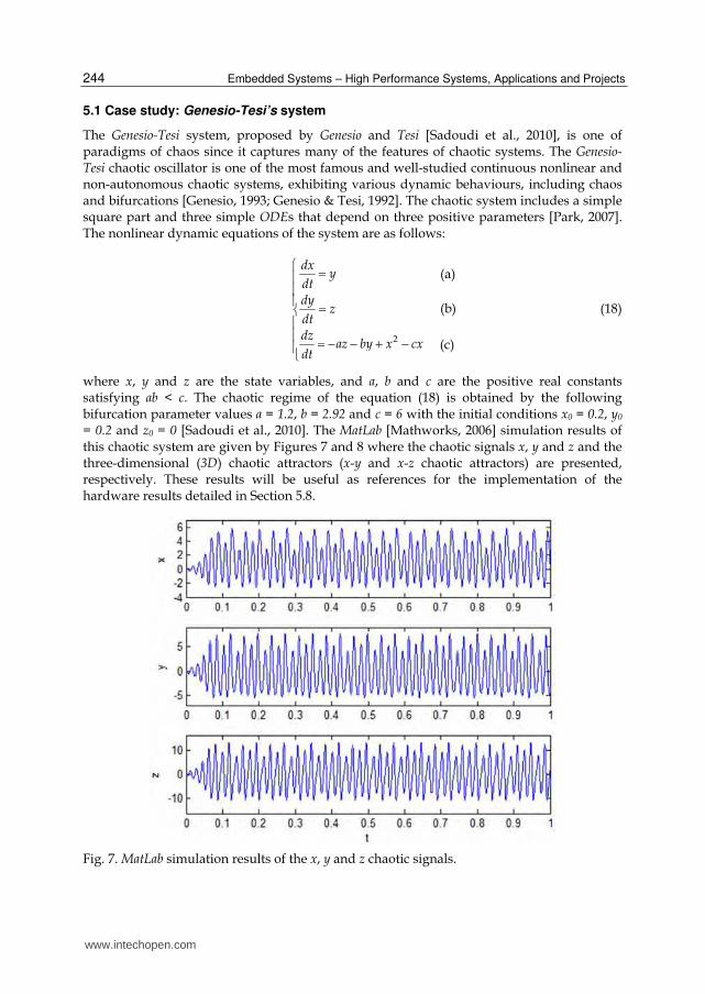
where x, y and z are the state variables, and a, b and c are the positive real constants satisfying ab < c. The chaotic regime of the equation (18) is obtained by the following bifurcation parameter values a = 1.2, b = 2.92 and c = 6 with the initial conditions x0 = 0.2, y0 = 0.2 and z0 = 0 [Sadoudi et al., 2010]. The MatLab [Mathworks, 2006] simulation results of this chaotic system are given by Figures 7 and 8 where the chaotic signals x, y and z and the three-dimensional (3D) chaotic attractors (x-y and x-z chaotic attractors) are presented, respectively. These results will be useful as references for the implementation of the hardware results detailed in Section 5.8.
Fig. 7. MatLab simulation results of the x, y and z chaotic signals.
(a)
(b)
(c)
www.intechopen.com
Hardware Design of Embedded Systems for Security Applications
245
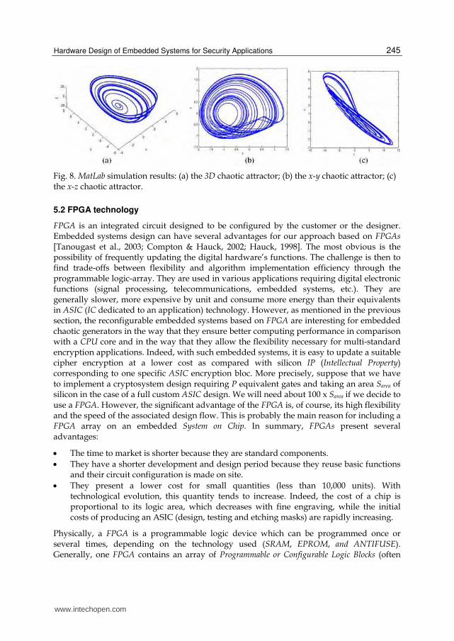
Fig. 8. MatLab simulation results: (a) the 3D chaotic attractor; (b) the x-y chaotic attractor; (c) the x-z chaotic attractor.
5.2 FPGA technology
FPGA is an integrated circuit designed to be configured by the customer or the designer. Embedded systems design can have several advantages for our approach based on FPGAs [Tanougast et al., 2003; Compton & Hauck, 2002; Hauck, 1998]. The most obvious is the possibility of frequently updating the digital hardware’s functions. The challenge is then to find trade-offs between flexibility and algorithm implementation efficiency through the programmable logic-array. They are used in various applications requiring digital electronic functions (signal processing, telecommunications, embedded systems, etc.). They are generally slower, more expensive by unit and consume more energy than their equivalents in ASIC (IC dedicated to an application) technology. However, as mentioned in the previous section, the reconfigurable embedded systems based on FPGA are interesting for embedded chaotic generators in the way that they ensure better computing performance in comparison with a CPU core and in the way that they allow the flexibility necessary for multi-standard encryption applications. Indeed, with such embedded systems, it is easy to update a suitable cipher encryption at a lower cost as compared with silicon IP (Intellectual Property) corresponding to one specific ASIC encryption bloc. More precisely, suppose that we have to implement a cryptosystem design requiring P equivalent gates and taking an area Sarea of silicon in the case of a full custom ASIC design. We will need about 100 x Sarea if we decide to use a FPGA. However, the significant advantage of the FPGA is, of course, its high flexibility and the speed of the associated design flow. This is probably the main reason for including a FPGA array on an embedded System on Chip. In summary, FPGAs present several advantages:
The time to market is shorter because they are standard components.
They have a shorter development and design period because they reuse basic functions and their circuit configuration is made on site.
They present a lower cost for small quantities (less than 10,000 units). With technological evolution, this quantity tends to increase. Indeed, the cost of a chip is proportional to its logic area, which decreases with fine engraving, while the initial costs of producing an ASIC (design, testing and etching masks) are rapidly increasing.
Physically, a FPGA is a programmable logic device which can be programmed once or several times, depending on the technology used (SRAM, EPROM, and ANTIFUSE). Generally, one FPGA contains an array of Programmable or Configurable Logic Blocks (often
www.intechopen.com
Embedded Systems – High Performance Systems, Applications and Projects
246
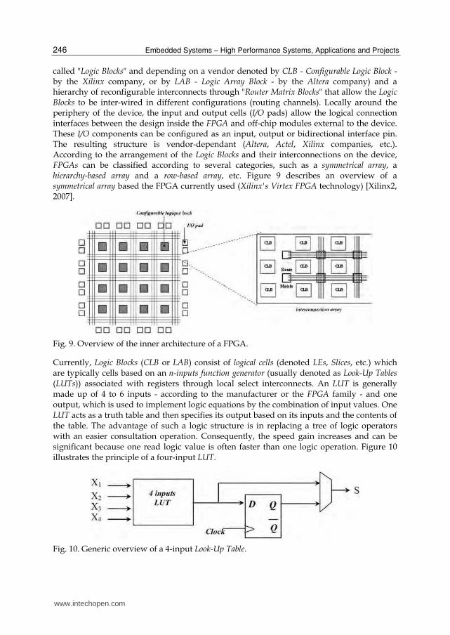
called "Logic Blocks" and depending on a vendor denoted by CLB - Configurable Logic Block - by the Xilinx company, or by LAB - Logic Array Block - by the Altera company) and a hierarchy of reconfigurable interconnects through "Router Matrix Blocks" that allow the Logic Blocks to be inter-wired in different configurations (routing channels). Locally around the periphery of the device, the input and output cells (I/O pads) allow the logical connection interfaces between the design inside the FPGA and off-chip modules external to the device. These I/O components can be configured as an input, output or bidirectional interface pin. The resulting structure is vendor-dependant (Altera, Actel, Xilinx companies, etc.). According to the arrangement of the Logic Blocks and their interconnections on the device, FPGAs can be classified according to several categories, such as a symmetrical array, a hierarchy-based array and a row-based array, etc. Figure 9 describes an overview of a symmetrical array based the FPGA currently used (Xilinx's Virtex FPGA technology) [Xilinx2, 2007].
Fig. 9. Overview of the inner architecture of a FPGA.
Currently, Logic Blocks (CLB or LAB) consist of logical cells (denoted LEs, Slices, etc.) which are typically cells based on an n-inputs function generator (usually denoted as Look-Up Tables (LUTs)) associated with registers through local select interconnects. An LUT is generally made up of 4 to 6 inputs - according to the manufacturer or the FPGA family - and one output, which is used to implement logic equations by the combination of input values. One LUT acts as a truth table and then specifies its output based on its inputs and the contents of the table. The advantage of such a logic structure is in replacing a tree of logic operators with an easier consultation operation. Consequently, the speed gain increases and can be significant because one read logic value is often faster than one logic operation. Figure 10 illustrates the principle of a four-input LUT.
Fig. 10. Generic overview of a 4-input Look-Up Table.
www.intechopen.com
Hardware Design of Embedded Systems for Security Applications
247
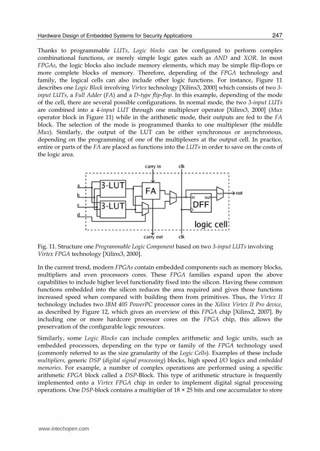
Thanks to programmable LUTs, Logic blocks can be configured to perform complex combinational functions, or merely simple logic gates such as AND and XOR. In most FPGAs, the logic blocks also include memory elements, which may be simple flip-flops or more complete blocks of memory. Therefore, depending of the FPGA technology and family, the logical cells can also include other logic functions. For instance, Figure 11 describes one Logic Block involving Virtex technology [Xilinx3, 2000] which consists of two 3-input LUTs, a Full Adder (FA) and a D-type flip-flop. In this example, depending of the mode of the cell, there are several possible configurations. In normal mode, the two 3-input LUTs are combined into a 4-input LUT through one multiplexer operator [Xilinx3, 2000] (Mux operator block in Figure 11) while in the arithmetic mode, their outputs are fed to the FA block. The selection of the mode is programmed thanks to one multiplexer (the middle Mux). Similarly, the output of the LUT can be either synchronous or asynchronous, depending on the programming of one of the multiplexers at the output cell. In practice, entire or parts of the FA are placed as functions into the LUTs in order to save on the costs of the logic area.
Fig. 11. Structure one Programmable Logic Component based on two 3-input LUTs involving Virtex FPGA technology [Xilinx3, 2000].
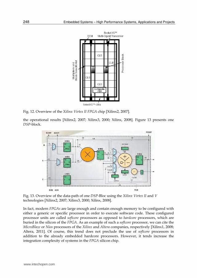
In the current trend, modern FPGAs contain embedded components such as memory blocks, multipliers and even processors cores. These FPGA families expand upon the above capabilities to include higher level functionality fixed into the silicon. Having these common functions embedded into the silicon reduces the area required and gives those functions increased speed when compared with building them from primitives. Thus, the Virtex II technology includes two IBM 405 PowerPC processor cores in the Xilinx Virtex II Pro device, as described by Figure 12, which gives an overview of this FPGA chip [Xilinx2, 2007]. By including one or more hardcore processor cores on the FPGA chip, this allows the preservation of the configurable logic resources.
Similarly, some Logic Blocks can include complex arithmetic and logic units, such as embedded processors, depending on the type or family of the FPGA technology used (commonly referred to as the size granularity of the Logic Cells). Examples of these include multipliers, generic DSP (digital signal processing) blocks, high speed I/O logics and embedded memories. For example, a number of complex operations are performed using a specific arithmetic FPGA block called a DSP-Block. This type of arithmetic structure is frequently implemented onto a Virtex FPGA chip in order to implement digital signal processing operations. One DSP-block contains a multiplier of 18 × 25 bits and one accumulator to store
www.intechopen.com
Embedded Systems – High Performance Systems, Applications and Projects
248
Fig. 12. Overview of the Xilinx Virtex II FPGA chip [Xilinx2, 2007].
the operational results [Xilinx2, 2007; Xilinx3, 2000; Xilinx, 2008]. Figure 13 presents one DSP-block.
Fig. 13. Overview of the data-path of one DSP-Bloc using the Xilinx Virtex II and V technologies [Xilinx2, 2007; Xilinx3, 2000; Xilinx, 2008].
In fact, modern FPGAs are large enough and contain enough memory to be configured with either a generic or specific processor in order to execute software code. These configured processor units are called softcore processors as opposed to hardcore processors, which are buried in the silicon of the FPGA. As an example of such a softcore processor, we can cite the MicroBlaze or Nios processors of the Xilinx and Altera companies, respectively [Xilinx1, 2008; Altera, 2011]. Of course, this trend does not preclude the use of softcore processors in addition to the already embedded hardcore processors. However, it tends increase the integration complexity of systems in the FPGA silicon chip.
www.intechopen.com
Hardware Design of Embedded Systems for Security Applications
249
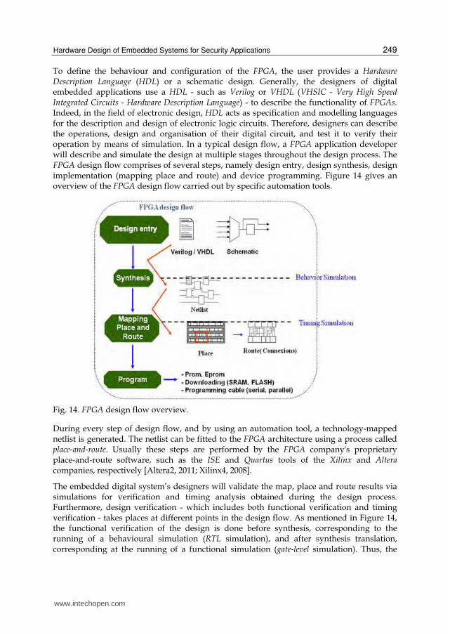
To define the behaviour and configuration of the FPGA, the user provides a Hardware Description Language (HDL) or a schematic design. Generally, the designers of digital embedded applications use a HDL - such as Verilog or VHDL (VHSIC - Very High Speed Integrated Circuits - Hardware Description Language) - to describe the functionality of FPGAs. Indeed, in the field of electronic design, HDL acts as specification and modelling languages for the description and design of electronic logic circuits. Therefore, designers can describe the operations, design and organisation of their digital circuit, and test it to verify their operation by means of simulation. In a typical design flow, a FPGA application developer will describe and simulate the design at multiple stages throughout the design process. The FPGA design flow comprises of several steps, namely design entry, design synthesis, design implementation (mapping place and route) and device programming. Figure 14 gives an overview of the FPGA design flow carried out by specific automation tools.
Fig. 14. FPGA design flow overview.
During every step of design flow, and by using an automation tool, a technology-mapped netlist is generated. The netlist can be fitted to the FPGA architecture using a process called place-and-route. Usually these steps are performed by the FPGA company's proprietary place-and-route software, such as the ISE and Quartus tools of the Xilinx and Altera companies, respectively [Altera2, 2011; Xilinx4, 2008].
The embedded digital system’s designers will validate the map, place and route results via simulations for verification and timing analysis obtained during the design process. Furthermore, design verification - which includes both functional verification and timing verification - takes places at different points in the design flow. As mentioned in Figure 14, the functional verification of the design is done before synthesis, corresponding to the running of a behavioural simulation (RTL simulation), and after synthesis translation, corresponding at the running of a functional simulation (gate-level simulation). Thus, the
www.intechopen.com
Embedded Systems – High Performance Systems, Applications and Projects
250
RTL description in VHDL or Verilog is initially simulated by creating test benches to simulate the system and observe the results. Next, the synthesis engine maps the design to a netlist. This netlist is translated to a gate-level description where simulation is repeated to confirm that the synthesis has proceeded without errors. Finally, the design is laid out in the FPGA, at which point propagation delays can be added and the simulation then runs again with these values back-annotated into the netlist. Once the design and validation process is complete, a binary file called bitstream is generated (also using the FPGA company's proprietary software) in order to (re)configure the FPGA. Therefore, the programming of the device is made from this programming file, containing the bits to program the specific FPGA by using a programming cable or by downloading into the device one memory file containing the bitstream. More precisely, the bitstream is transferred to the FPGA/CPLD via a serial interface (JTAG - Joint Test Action Group - standard support) or to an external memory device, such as an EEPROM or a PROM. Generally, after the device’s programming, a circuit verification is done in order to verify the real and final functionality of the design. This final step allows for the specification of real performance in terms of power consumption, work frequency and the required logic, as well as memory hardware resources. Furthermore, in order to simplify the design of complex systems in FPGAs, there exist libraries of predefined complex functions and circuits that have been tested and optimised so as to speed up the design process. These predefined circuits are commonly called IP cores, and are available from FPGA vendors and third-party IP suppliers (under proprietary licenses). These modules are available for targeting and programming FPGA hardware. Other predefined circuits are also available from developer communities, such as the OpenCores site (typically released under free and open-source licenses) [Opencores].
Thanks to such structures, a FPGA can be used to implement any logical function that an ASIC could perform. The ability to update their functionality after shipping (defined as total or partial chip reconfiguration of a portion of the design and the low non-recurring engineering costs relative to an ASIC design) offers advantages for many embedded applications. Thus, the FPGA allows for even higher performance by trading off precision and an increased number of parallel arithmetic units. Indeed, the inherent parallelism of the logic resources on a FPGA allows for considerable computational throughput, even at low MHz clock-rates. The adoption of FPGAs in high performance computing is currently limited by the complexity of FPGA design compared with conventional software. Indeed, the place and route steps for a complex design may take a long time to succeed.
In the case of the implementation of an embedded chaotic system, an optimised hardware design coded into a VHDL with a structural description logic is required. Indeed, the ‘‘high level’’ aspect of one non-optimal VHDL code generation keeps the embedded designer far removed from the realities of physical implementation, which does not allow for the optimised performance of the design. Consequently, a result in terms of performance and the density of resources used remains out of the designer’s reach. Therefore, the designers of embedded system based on FPGAs must find applications in any area or with any algorithm which can make use of the massive parallelism offered by the architecture. One such area is to design one cryptosystem allowing the avoidance of the breaking of the code - in particular brute-force attacks - of cryptographic algorithms carried out by the digital circuit. In this context, and in considering our embedded ciphering application, hardware implementation is designed and coded in VHDL with a structural description logic. This low level form of design seeks for resolving the Genesio-Tesi differential equation (18) through the
www.intechopen.com
Hardware Design of Embedded Systems for Security Applications
251
RK-4 numerical resolution method in order to produce a more accurate estimate of the solution [Cartwright & Piro, 1992].
The FPGA implementation presented in the remainder of this section will simulate the correct operation with test vectors returned by the software’s implementation.
5.3 RTL architecture
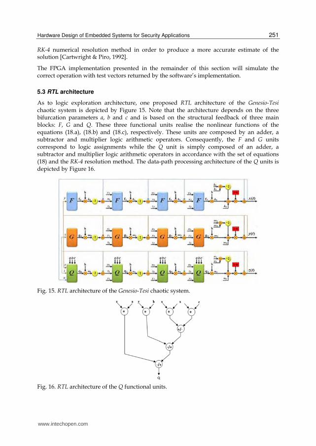
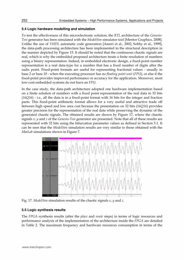
As to logic exploration architecture, one proposed RTL architecture of the Genesio-Tesi chaotic system is depicted by Figure 15. Note that the architecture depends on the three bifurcation parameters a, b and c and is based on the structural feedback of three main blocks: F, G and Q. These three functional units realise the nonlinear functions of the equations (18.a), (18.b) and (18.c), respectively. These units are composed by an adder, a subtractor and multiplier logic arithmetic operators. Consequently, the F and G units correspond to logic assignments while the Q unit is simply composed of an adder, a subtractor and multiplier logic arithmetic operators in accordance with the set of equations (18) and the RK-4 resolution method. The data-path processing architecture of the Q units is depicted by Figure 16.
Fig. 15. RTL architecture of the Genesio-Tesi chaotic system.
Fig. 16. RTL architecture of the Q functional units.
www.intechopen.com
Embedded Systems – High Performance Systems, Applications and Projects
252
5.4 Logic hardware modelling and simulation
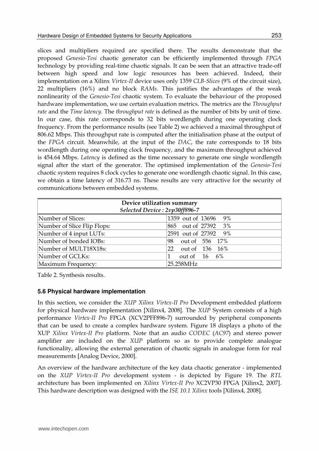
To test the effectiveness of this microelectronic solution, the RTL architecture of the Genesio-Tesi generator has been simulated with the ModelSim simulator tool [Mentor Graphics, 2008]. Unlike the use of VHDL automatic code generation [Aseeri et al., 2002; Sobhy et al., 1999], the data-path processing architecture has been implemented in the structural description in the manner depicted by Figure 15. It should be noted that the continuous chaotic signals are real, which is why the embedded proposed architecture treats a finite resolution of numbers using a binary representation. Indeed, in embedded electronic design, a fixed-point number representation is a real data-type for a number that has a fixed number of digits after the radix point. Fixed-point formats are useful for representing fractional values - usually in base 2 or base 10 - when the executing processor has no floating point unit (FPU), or else if the fixed-point provides improved performance or accuracy for the application. Moreover, most low-cost embedded systems do not have an FPU.
In the case study, the data-path architecture adopted one hardware implementation based on a finite solution of numbers with a fixed point representation of the real data in 32 bits (16Q16) - i.e., all the data is in a fixed-point format with 16 bits for the integer and fraction parts. This fixed-point arithmetic format allows for a very useful and attractive trade off between high speed and low area cost because the presentation on 32 bits (16Q16) provides greater precision for the representation of the real data while preserving the dynamic of the generated chaotic signals. The obtained results are shown by Figure 17, where the chaotic signals x, y and z of the Genesio-Tesi generator are presented. Note that all of these results are represented with 32 bits using the bifurcation parameter values as defined in Section 5.1. It can be seen that the ModelSim simulation results are very similar to those obtained with the MatLab simulations shown in Figure 7.
Fig. 17. ModelSim simulation results of the chaotic signals x, y and z.
5.5 Logic synthesis results
The FPGA synthesis results (after the place and route steps) in terms of logic resources and
performance analysis of the implementation of the architecture inside the FPGA are detailed
in Table 2. The maximum frequency and hardware resources consumption in terms of the
www.intechopen.com
Hardware Design of Embedded Systems for Security Applications
253
slices and multipliers required are specified there. The results demonstrate that the
proposed Genesio-Tesi chaotic generator can be efficiently implemented through FPGA
technology by providing real-time chaotic signals. It can be seen that an attractive trade-off
between high speed and low logic resources has been achieved. Indeed, their
implementation on a Xilinx Virtex-II device uses only 1359 CLB-Slices (9% of the circuit size),
22 multipliers (16%) and no block RAMs. This justifies the advantages of the weak
nonlinearity of the Genesio-Tesi chaotic system. To evaluate the behaviour of the proposed
hardware implementation, we use certain evaluation metrics. The metrics are the Throughput
rate and the Time latency. The throughput rate is defined as the number of bits by unit of time.
In our case, this rate corresponds to 32 bits wordlength during one operating clock
frequency. From the performance results (see Table 2) we achieved a maximal throughput of
806.62 Mbps. This throughput rate is computed after the initialisation phase at the output of
the FPGA circuit. Meanwhile, at the input of the DAC, the rate corresponds to 18 bits
wordlength during one operating clock frequency, and the maximum throughput achieved
is 454.64 Mbps. Latency is defined as the time necessary to generate one single wordlength
signal after the start of the generator. The optimised implementation of the Genesio-Tesi
chaotic system requires 8 clock cycles to generate one wordlength chaotic signal. In this case,
we obtain a time latency of 316.73 ns. These results are very attractive for the security of
communications between embedded systems.
Device utilization summary Selected Device : 2vp30ff896-7
Number of Slices: 1359 out of 13696 9%
Number of Slice Flip Flops: 865 out of 27392 3%
Number of 4 input LUTs: 2591 out of 27392 9%
Number of bonded IOBs: 98 out of 556 17%
Number of MULT18X18s: 22 out of 136 16%
Number of GCLKs: 1 out of 16 6%
Maximum Frequency: 25.258MHz
Table 2. Synthesis results.
5.6 Physical hardware implementation
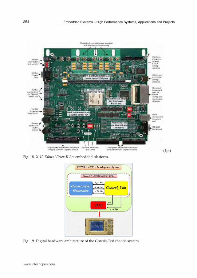
In this section, we consider the XUP Xilinx Virtex-II Pro Development embedded platform
for physical hardware implementation [Xilinx4, 2008]. The XUP System consists of a high
performance Virtex-II Pro FPGA (XCV2PFF896-7) surrounded by peripheral components
that can be used to create a complex hardware system. Figure 18 displays a photo of the
XUP Xilinx Virtex-II Pro platform. Note that an audio CODEC (AC97) and stereo power
amplifier are included on the XUP platform so as to provide complete analogue
functionality, allowing the external generation of chaotic signals in analogue form for real
measurements [Analog Device, 2000].
An overview of the hardware architecture of the key data chaotic generator - implemented
on the XUP Virtex-II Pro development system - is depicted by Figure 19. The RTL
architecture has been implemented on Xilinx Virtex-II Pro XC2VP30 FPGA [Xilinx2, 2007].
This hardware description was designed with the ISE 10.1 Xilinx tools [Xilinx4, 2008].
www.intechopen.com
Embedded Systems – High Performance Systems, Applications and Projects
254
(4pt)
Fig. 18. XUP Xilinx Virtex-II Pro embedded platform.
Fig. 19. Digital hardware architecture of the Genesio-Tesi chaotic system.
www.intechopen.com
Hardware Design of Embedded Systems for Security Applications
255
The architecture system consists of two main modules: the Control_Unit and the Genesio-Tesi-Generator module. The Control_Unit module is a Moore-state machine which manages and schedules the different operations and functions of the chaotic system. The Genesio-Tesi-Generator module generates the chaotic signals as described in Section 5.4. Once the chaotic signals (x, y and z) with 32 bits wordlength are obtained, they are truncated to 18 bits and converted to an analogue format using a Digital-to-Analogue Converter (DAC), and this process is then repeated. Next, the real-time chaotic signals obtained at the output of the DAC are visualised via a digital oscilloscope [Agilent, 2007]. Note that this proposed architecture offers two different means for using the obtained real-time chaotic signals. Indeed, it permits the use of them in their analogue form at the output of the DAC or their use in their digital form directly at the output of the FPGA circuit. This will permit the easy exploitation of the richness of the dynamical behaviour of the embedded Genesio-Tesi chaotic generator for such embedded applications as communications security.
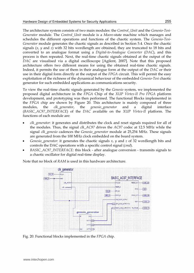
To view the real-time chaotic signals generated by the Genesio system, we implemented the proposed digital architecture in the FPGA Chip of the XUP Virtex-II Pro FPGA platform development, and prototyping was then performed. The functional Blocks implemented in the FPGA chip are shown by Figure 20. This architecture is mainly composed of three modules, the clk_generator, the genesio_generator and a digital interface (BASIC_AC97_INTERFACE) of the DAC available on the XUP Virtex-II platform. The functions of each module are:
clk_generator: it generates and distributes the clock and reset signals required for all of the modules. Thus, the signal clk_AC97 drives the AC97 codec at 12.5 MHz while the signal clk_genesio cadences the Genesio_generator module at 25,254 MHz. These signals are generated from the 100 MHz clock embedded on the board system.
Genesio_generator: it generates the chaotic signals x, y and z of 32 wordlength bits and controls the DAC operations with a specific control signal (cmd).
BASIC_AC97_INTERFACE: this block - after analogue conversion - transmits signals to a chaotic oscillator for digital real-time display.
Note that no block of RAM is used in this hardware architecture.
Fig. 20. Functional blocks implemented in the FPGA chip.
www.intechopen.com
Embedded Systems – High Performance Systems, Applications and Projects
256
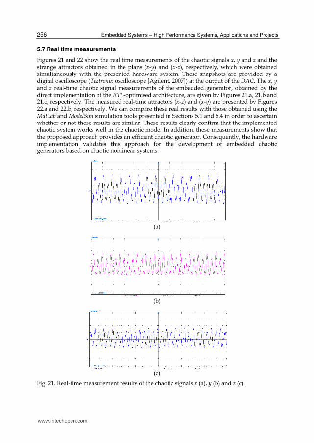
5.7 Real time measurements
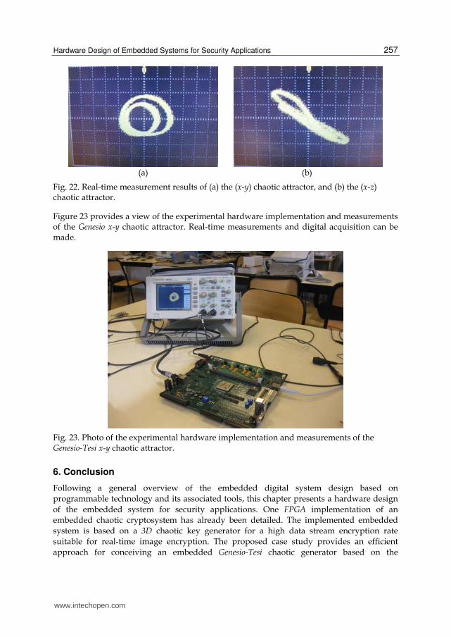
Figures 21 and 22 show the real time measurements of the chaotic signals x, y and z and the strange attractors obtained in the plans (x-y) and (x-z), respectively, which were obtained simultaneously with the presented hardware system. These snapshots are provided by a digital oscilloscope (Tektronix oscilloscope [Agilent, 2007]) at the output of the DAC. The x, y and z real-time chaotic signal measurements of the embedded generator, obtained by the direct implementation of the RTL-optimised architecture, are given by Figures 21.a, 21.b and 21.c, respectively. The measured real-time attractors (x-z) and (x-y) are presented by Figures 22.a and 22.b, respectively. We can compare these real results with those obtained using the MatLab and ModelSim simulation tools presented in Sections 5.1 and 5.4 in order to ascertain whether or not these results are similar. These results clearly confirm that the implemented chaotic system works well in the chaotic mode. In addition, these measurements show that the proposed approach provides an efficient chaotic generator. Consequently, the hardware implementation validates this approach for the development of embedded chaotic generators based on chaotic nonlinear systems.
(a)
(b)
(c)
Fig. 21. Real-time measurement results of the chaotic signals x (a), y (b) and z (c).
www.intechopen.com
Hardware Design of Embedded Systems for Security Applications
257
(a) (b)
Fig. 22. Real-time measurement results of (a) the (x-y) chaotic attractor, and (b) the (x-z) chaotic attractor.
Figure 23 provides a view of the experimental hardware implementation and measurements of the Genesio x-y chaotic attractor. Real-time measurements and digital acquisition can be made.
Fig. 23. Photo of the experimental hardware implementation and measurements of the Genesio-Tesi x-y chaotic attractor.
6. Conclusion
Following a general overview of the embedded digital system design based on
programmable technology and its associated tools, this chapter presents a hardware design
of the embedded system for security applications. One FPGA implementation of an
embedded chaotic cryptosystem has already been detailed. The implemented embedded
system is based on a 3D chaotic key generator for a high data stream encryption rate
suitable for real-time image encryption. The proposed case study provides an efficient
approach for conceiving an embedded Genesio-Tesi chaotic generator based on the
www.intechopen.com
Embedded Systems – High Performance Systems, Applications and Projects
258
implementation of reconfigurable technology. The hardware implementation of this
embedded generator gave attractive performances. More precisely, the implementation
requires only 1359 CLB-slices, 22 multipliers and no blocks of RAM, and achieves a
throughput rate of 808.26 Mbps at the output of the FPGA circuit and 454.64 Mbps at the
input of the DAC, with a clock frequency of 25.258 MHz and with a low latency time of
316.73 ns. Thus, the signal generator performs well for embedded applications, such as
secure communications based on chaos approach. The random key generator architecture
that was presented is particularly attractive, since it provides low-cost secure
communications solutions for embedded systems. This approach at hardware design is
validated by showing that the real-time Genesio-Tesi chaotic signals obtained with the RTL
architecture are similar to the software simulations as its counterparts. Moreover, embedded
cipher systems can have several advantages over the use of FPGAs. Indeed, the
experimental results using the Xilinx Virtex technology have demonstrated that the design
approach presented can lead to designs with a small logic area, satisfactory throughput rates
and low latency for embedded applications.
7. References
Agilent, (2007). 3000 Series Oscilloscopes data Sheet, Agilent Technologies, 5989-2235. Altera. (2011). Nios II Processor, Reference Handbook; Available from http://www. altera.com Altera2, (2011). Quartus II Handbook Version 11.1. Available from http://www.altera.com/literature/hb/qts/quartusii_handbook.pdf Analog Device, (2000), AC’97 SoundMAX Codec, AD1881A Datasheet. Aseeri, M. A.; Sobhy, M. I.; Lee, P. (2002). Lorenz Chaotic Model Using Field Programmable
Gate Array (FPGA), Midwest Symposium on Circuit and Systems, pp. 686-699. Azzaz, M. S.; Tanougast, C.; Sadoudi, S.; Dandache, A. (2011). Robust Chaotic Key Stream
Generator for Real Time Images Encryption, Journal of Real-Time Image Processing, Springer Verlag, Vol. 6.
Brown, S.; Rose, J. (1996). FPGA and CPLD architectures: a tutorial, IEEE Design and Test of Computers, 13 (2), pp. 42–57.
Burr, W. E. (2003). Selecting the advanced Encryption Standard, IEEE Security & Privacy, IEEE Computer Society, pp. 43-52.
Carroll, P. L.; Pecora, L. M. (1990). Synchronization in chaotic systems, Phy. Rev. Lett., 64 (8), pp. 821-824.
Cartwright, J. H. E.; Piro, O. (1992). The Dynamics of Runge-Kutta Methods, Int. J. Bifurcation and Chaos, Vol. 2, pp. 427-449.
Cha, C. Y.; Lee, S. G. (2005). Complementary Colpitts Oscillator in CMOS Technology’, IEEE Transaction on microwave theory and techniques, 53 (3).
Chen, H. H ; Chiang, J. S. ; Lin, Y. L. ; Lee, C. I. (2007). Chaos synchronization of general Lorenz, Lü, and Chen systems, HSIUPING Journal, Vol. 15, pp. 159-166.
Compton, K.; Hauck, S. (2002). Reconfigurable computing : a survey of systems and software, ACM Comput. Surv., 34 (2), pp. 171 - 210.
Cuomo, K. M.; Oppenheim, A. V.; Strogatz, S. H. (1993). Synchronization of Lorenz-Based Chaotic Circuits with Applications to Communications, IEEE transactions on circuits and systems-11: analog and digital signal processing, 40 (1), pp. 626-633.
www.intechopen.com
Hardware Design of Embedded Systems for Security Applications
259
Genesio, R.; Tesi, A.; Villoresi, F. (1993). A frequency approach for analyzing and controlling chaos in nonlinear circuits, IEEE Trans. on Circuits Systems I: Fundamental Theory and Applications. Vol. 40, pp. 819-828.
Genesio, R; Tesi, A. (1992). Harmonic balance methods for the analysis of chaotic dynamics in nonlinear systems, Automatica, Vol. 28, pp. 531–548.
Giannakopoulos, K.; Souliotis, G.; Fragoulis, N. (2007). An integratable chaotic oscillator with Current Amplifiers, IEEE Int Symp. on Signals, Circuits and Systems, Vol. 1, pp. 1-4.
Hauck, S. (1998). The role of FPGA in reprogrammable systems, Proceedings of IEEE, Vol. 86 ( 4), pp. 615–638.
Indrusiak, L. S.; Dutra Silva Junior, E.C. ; Glesner, M. (2005). Advantages of the Linz-Sprott weak nonlinearity on the FPGA implementation of chaotic systems: a comparative analysis, Proc. Int. Symp. Signals, Circuits and Sys. 2, pp. 753 – 756.
Kennedy, M. P. (1994). Chaos in the Colpitts oscillator, IEEE Trans. Circuits Syst. I, Vol. 41, pp. 771-774.
Kvarda, P. (2002). Investigating the Rössler attractor using Lorenz plot and Lyapunov exponents, Radio Engineering. 11 (3), pp. 22-23.
Liu, T.; Tanougast, C.; Brunet, P.; Berviller, Y.; Rabah H.; Weber, S. (2005). An Optimized FPGA Implementation of an AES Algorithm for Embedded Applications, The International Workshop on Applied Reconfigurable Computing, pp. 111-118.
Lorenz, T E.N. (1963). Deterministic nonperiodic flow, Journal of the Atmospheric Sciences, 20 (2), pp. 130-141.
Lü, J.; Chen, G. (2002). A new chaotic attractor coined, Int. Journal of Bifurcation and Chaos, 12 (3), pp. 659-661.
Mathworks (2006), MatLab Software, Version 7.3, Mathworks. Matsumoto, T. (1987). Chaos in electronic circuits, Proc of the IEEE, Vol. 75 (8), pp. 1033-1046. Mentor Graphics, (2008). Modelsim SE User’s Manuel, Software, Version 6. 4, Mentor
Graphics. Opencores, Available from http://opencores.org. Ozoguz, S. ; Ates, O.; Elwakil, A. S. O. (2005). An integrated circuit chaotic oscillator and its
application for high speed random bit generation, ISCAS 2005, Vol. 5, pp. 4345- 4348.
Park, J. H. (2007). Exponential Synchronization of the Genesio-Tesi Chaotic System via a Novel Feedback Control,” Phys.Scr., Vol. 76, pp. 617-622.
Sadoudi, S.; Tanougast, C.; Azzaz, M.; Bouridane, A. Dandache, A. (2010). Embedded Genesio-Tesi Chaotic Generator for cipher communications, 7th IEEE, IET International Symposium on Communication Systems, Networks and Digital Signal Processing, pp. 234 - 238.
Sobhy, M. I.; Aseeri, M. A.; Shehata, A. E. R. (1999). Real Time Implementation Of Continuous (Chua And Lorenz) Chaotic Generator Models Using Digital Hardware, Proc. of the Third International Symposium on Communication Systems Networks and Digital Processing, pp. 38-41.
Sorel, Y. (1994). Massively parallel systems with real time constraints, the algorithm architecture adequation methodology, In Proceedings of Conference on Massively Parallel Computing Systems, May 1994, pp. 44 - 53.
www.intechopen.com
Embedded Systems – High Performance Systems, Applications and Projects
260
Tanougast, C.; Berviller, Y.; Weber, S.; Brunet, P. (2003). A partitioning methodology that optimises the area on reconfigurable real-time embedded systems, EURASIP Journal On Applied Signal Processing, Special Issue on Rapid Prototyping of DSP Systems, Vol. ( 6), pp. 494-501.
Tanougast, C.; Berviller, Y.; Brunet, P.; Weber, S.; Rabah, H. (2003). Temporal partitioning methodology optimizing FPGA resources for dynamically reconfigurable embedded real-time system, Microprocessors and Microsystems, Elsevier, 27 (3), pp. 115-130.
Yang, T. (2004). A survey of chaotic secure communication systems, International Journal of Computational Cognition, 2 (2), pp. 81-130.
Yang, Cao, Chung and Morris, (2005). Applied Numerical Methods Using MATLAB, John Wiley, and Sons, Inc.
Xilinx1. (2008). MicroBlaze Processor, Reference Guide Embedded Development Kit EDK 10.1i, UG081 (v9.0). Available from
http://www.xilinx.com/support/documentation/sw_manuals/mb_ref_guide.pdf Xilinx2, (2007). VirtexII complete Datasheet. Available from http://www.xilinx.com/support/documentation/data_sheets/ds031.pdf. Xilinx3, (2000). Xilinx Data Sheet DS003 (v.2.2). Xilinx, (2008). Virtex5 FPGA Data Sheet, 2008. Available from http://www.xilinx.com/support/documentation/data_sheets/ds202.pdf. Xilinx4, (2008). Integrated Software Environment (ISE), Version 10.1, Available from http://www.xilinx.com/support/documentation Xilinx4, (2008). Xilinx University Program Virtex-II Pro Development System, Xilinx, UG069
(v1.1).
www.intechopen.com
Embedded Systems - High Performance Systems, Applications andProjectsEdited by Dr. Kiyofumi Tanaka
ISBN 978-953-51-0350-9Hard cover, 278 pagesPublisher InTechPublished online 16, March, 2012Published in print edition March, 2012
InTech EuropeUniversity Campus STeP Ri Slavka Krautzeka 83/A 51000 Rijeka, Croatia Phone: +385 (51) 770 447 Fax: +385 (51) 686 166www.intechopen.com
InTech ChinaUnit 405, Office Block, Hotel Equatorial Shanghai No.65, Yan An Road (West), Shanghai, 200040, China
Phone: +86-21-62489820 Fax: +86-21-62489821
Nowadays, embedded systems - computer systems that are embedded in various kinds of devices and play animportant role of specific control functions, have permeated various scenes of industry. Therefore, we canhardly discuss our life or society from now onwards without referring to embedded systems. For wide-rangingembedded systems to continue their growth, a number of high-quality fundamental and applied researches areindispensable. This book contains 13 excellent chapters and addresses a wide spectrum of research topics ofembedded systems, including parallel computing, communication architecture, application-specific systems,and embedded systems projects. Embedded systems can be made only after fusing miscellaneoustechnologies together. Various technologies condensed in this book as well as in the complementary book"Embedded Systems - Theory and Design Methodology", will be helpful to researchers and engineers aroundthe world.
How to referenceIn order to correctly reference this scholarly work, feel free to copy and paste the following:
Camel Tanougast, Abbas Dandache, Mohamed Salah Azzaz and Said Sadoudi (2012). Hardware Design ofEmbedded Systems for Security Applications, Embedded Systems - High Performance Systems, Applicationsand Projects, Dr. Kiyofumi Tanaka (Ed.), ISBN: 978-953-51-0350-9, InTech, Available from:http://www.intechopen.com/books/embedded-systems-high-performance-systems-applications-and-projects/hardware-design-of-embedded-systems-for-security-applications

© 2012 The Author(s). Licensee IntechOpen. This is an open access articledistributed under the terms of the Creative Commons Attribution 3.0License, which permits unrestricted use, distribution, and reproduction inany medium, provided the original work is properly cited.