Embed Size (px)
Citation preview

This article was downloaded by: 10.3.98.104On: 11 Feb 2022Access details: subscription numberPublisher: CRC PressInforma Ltd Registered in England and Wales Registered Number: 1072954 Registered office: 5 Howick Place, London SW1P 1WG, UK
Handbook of NanophysicsNanotubes and NanowiresKlaus D. Sattler
Electron Transport in Carbon Nanotubes
Publication detailshttps://www.routledgehandbooks.com/doi/10.1201/9781420075434-5
Na Young KimPublished online on: 17 Sep 2010
How to cite :- Na Young Kim. 17 Sep 2010, Electron Transport in Carbon Nanotubes from: Handbookof Nanophysics, Nanotubes and Nanowires CRC PressAccessed on: 11 Feb 2022https://www.routledgehandbooks.com/doi/10.1201/9781420075434-5
PLEASE SCROLL DOWN FOR DOCUMENT
Full terms and conditions of use: https://www.routledgehandbooks.com/legal-notices/terms
This Document PDF may be used for research, teaching and private study purposes. Any substantial or systematic reproductions,re-distribution, re-selling, loan or sub-licensing, systematic supply or distribution in any form to anyone is expressly forbidden.
The publisher does not give any warranty express or implied or make any representation that the contents will be complete oraccurate or up to date. The publisher shall not be liable for an loss, actions, claims, proceedings, demand or costs or damageswhatsoever or howsoever caused arising directly or indirectly in connection with or arising out of the use of this material.
Dow
nloa
ded
By:
10.
3.98
.104
At:
16:1
1 11
Feb
202
2; F
or: 9
7814
2007
5434
, cha
pter
3, 1
0.12
01/9
7814
2007
5434
-5
3-1
3.1 Introduction
Carbon (6C) exists ubiquitously in nature. It is the fourth most abundant element by mass aft er hydrogen, helium, and oxygen. Carbon has four valence electrons in 2s and 2p orbitals that can form three hybridization arrangements: sp, sp2, and sp3. Via these hybrid orbitals, carbon can bond to themselves and to other elements. Even with the carbon element only, there are many systems with distinct properties: diamond, graphene, and buckyball fullerene C60 (Figure 3.1c). It is mysterious that carbon bonding in diamond can be as strong as to scribe other crystals, but in graphite as weak as to scribble on paper.
In 1991, graphitic needle-like carbon structures were synthe-sized fortuitously in a furnace that was used to produce C60 and other fullerene structures (Figure 3.1d, Iijima 1991). Since such concentric cylindrical structures were unprecedented, in early literature they were denoted as “microtubules” (Iijima 1991), “fullerene tubules” (Mintmire et al. 1992), or “graphene tubules” (Saito et al. 1992), before the term carbon nanotube (CNT) was coined. Th ese early terms refl ected the diff erent perspectives of newly discovered structures. One school of thought believed that CNTs could be elongated from fullerene as mutations, while another school of thought believed that they could be formed by folding several graphene layers seamlessly. Although the start-ing material to make needle-like carbon structures from these two thoughts was not the same, both perspectives commonly envisioned CNTs as one-dimensional (1D) objects. A high geo-metric ratio of length to diameter (105–106) indeed supports this 1D picture from experimental statistical analyses that diameters are typically up to a few tens of nanometers and lengths are in microns and even in millimeters.
One-dimensional systems are very special in comparison to their two-dimensional or three-dimensional counterparts in that there is only one particular direction along which par-ticles can move freely while they are strongly confi ned along two other directions. Hence, scientists and engineers have longed for a physical medium to explore unique 1D properties and have searched for alternative structures to attain miniaturization. Shortly aft er their discovery, CNTs have been one of the hot research topics in investigating low-dimensional properties in a variety of disciplines in science and engineering.
Many researchers have been intrigued by the CNTs’ extraor-dinary mechanical, chemical, optical, and electrical properties and their fabrication advantages (low cost and defect-free crys-talline structure) (Saito et al. 1998, Harris 1999, Jorio et al. 2008). Indeed, CNTs have already been infl uential in widespread areas as sensitive chemical sensors, high-resolution imaging probes, fi eld emission displays, supercapacitors, conductive fl exible elec-trodes, and more. In particular, CNTs have been regarded as potentially promising for future molecular electronics based on their phenomenal electrical characteristics and naturally small sizes (Dekker 1999). For example, high-performance nanotube fi eld eff ect transistors have been demonstrated with semicon-ducting tubes (Bockrath et al. 1997, Javey et al. 2003), and the interplay of electrons and phonons in CNT transistors was thor-oughly examined in order to develop practical room-temperature electronics (Yao et al. 2000, Javey et al. 2004, Park et al. 2004). Due to the spatial confi nement in 1D where electrons can move only back and forth in principle, several questions naturally arise: How do electrons carry electrical information in 1D conductors like CNTs? What are the unique electrical phenomena occurring in 1D conductors?
3Electron Transport
in Carbon Nanotubes
3.1 Introduction .............................................................................................................................3-13.2 Fundamental Concepts ...........................................................................................................3-2
Overview of Carbon Nanotube Transport • Electron Transport • Fermi-Liquid vs. Non- Fermi-Liquid Th eories
3.3 Electron Transport in Carbon Nanotubes ...........................................................................3-6Synthesis and Device Fabrication • Diff erential Conductance • Low-Frequency Shot Noise
3.4 Summary ................................................................................................................................. 3-113.5 Future Perspective ................................................................................................................. 3-11References ........................................................................................................................................... 3-11
Na Young KimStanford University

Dow
nloa
ded
By:
10.
3.98
.104
At:
16:1
1 11
Feb
202
2; F
or: 9
7814
2007
5434
, cha
pter
3, 1
0.12
01/9
7814
2007
5434
-53-2 Handbook of Nanophysics: Nanotubes and Nanowires
Th is chapter describes the fundamental concepts and recent progress in CNT electron transport fi elds. Electron transport measurements are convenient methods for characterizing mate-rials in order to study the underlying physical principles. By applying external stimulations, the corresponding response of materials provides an answer to the question of how electrons fl ow through them. Section 3.2 provides an overview of CNT electron transport research areas and presents several basic concepts and terminologies of quantum electron transport and two theoretical frameworks pertinent for interpreting CNT transport properties. Based on these fundamentals, Section 3.3 develops the details of quantum electron transport measure-ments using metallic single-walled carbon nanotubes in terms of diff erential conductance and shot noise. A summary of the discussion and future perspectives are given in Sections 3.4 and 3.5, respectively.
3.2 Fundamental Concepts
3.2.1 Overview of Carbon Nanotube Transport
CNTs are regarded as one of the ideal 1D systems and a good candidate for exploring low dimensional physics. Th e basic elec-tronic understanding of CNTs starts from their band structure. Shortly aft er the discovery of concentric multi-layered carbon tubules in 1991, condensed matter theorists immediately estab-lished the theoretical framework to compute the band structure
of CNTs by extending the two-dimensional graphene knowl-edge. Th ey fi rst simplifi ed a target system as one single tube that was conceptually folded from one graphene layer even before such tubes were physically identifi ed (Mintmire et al. 1992, Saito et al. 1992).
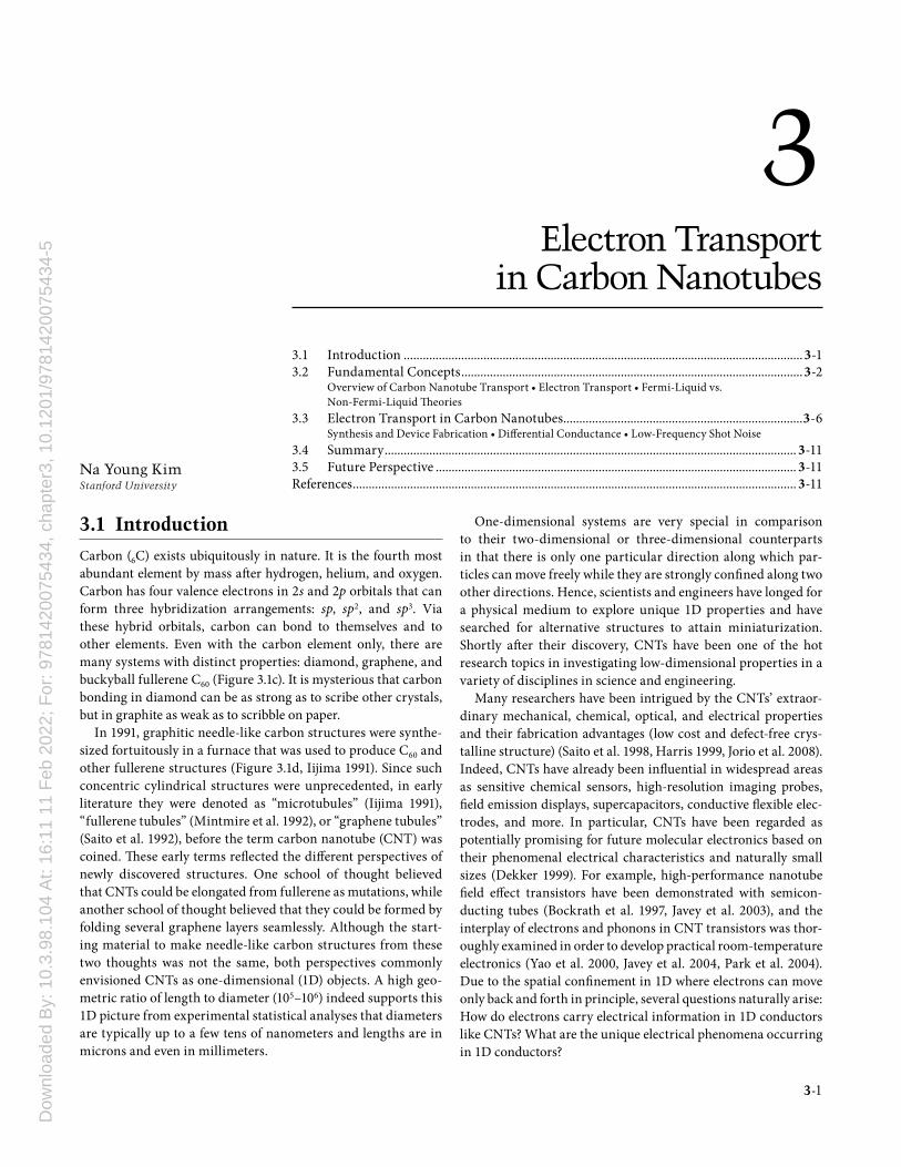
Figure 3.2 depicts how to form CNTs from a sheet of graphene by rolling up along a certain direction with a diff erent diameter. A (n, m) confi guration classifi es possible nanotubes in terms of the integer coeffi cients of the two-dimensional roll-up vector ( hC�
, Figure 3.2b, Saito et al. 1992). Th is (n, m) confi guration is a compact representation to specify diameters and chirali-ties of CNTs. A spatial confi nement along the circumferential direction in CNTs requires satisfying a periodic boundary con-dition. Th us, by including this additional boundary condition into the well-established graphite band structure calculation (Wallace 1947), the CNT band structure was readily computed (Mintmire et al. 1992, Saito et al. 1992).
Condensed matter theorists conjectured from the band struc-ture calculation that such tubules would exhibit either metal-lic or semiconducting behavior depending on the values of n, m (Mintmire et al. 1992, Saito et al. 1992). When n-m is an integer in multiples of 3, the (n, m) nanotubes will be metallic. Specifi c terms became available according to theoretical insights: single-walled nanotubes (SWNTs) and multi-walled nano-tubes (MWNTs) are distinguished by the number of constitu-ent layers; armchair (n = m) and zigzag tubes (n = 0 or m = 0) indicate a hexagonal arrangement around the circumference.
(a)
(b)
(c)
(d)
a b c
3 nm
(e)
FIGURE 3.1 (a) A cartoon of the 6C atomic shell structure in a semiclassical picture. (b) Th e diagram of s- and p-orbital hybridization: linear sp (left ), planer sp2 (middle), and tetrahedral sp3 (right). (c) Structures of carbon-based material: C60 (left ), diamond (middle), and graphite (right). (d) Electron micrograph of multi-walled carbon nanotubes. (Reprinted from Iijima, S., Nature, 354, 56, 1991. With permission.) (e) An electron micrograph of single-walled carbon nanotubes. (Reprinted from Iijima, S. and Ichihashi, T., Nature, 363, 603, 1993. With permission.)
Dow
nloa
ded
By:
10.
3.98
.104
At:
16:1
1 11
Feb
202
2; F
or: 9
7814
2007
5434
, cha
pter
3, 1
0.12
01/9
7814
2007
5434
-5Electron Transport in Carbon Nanotubes 3-3
Furthermore, these theoretical conjectures were initiated to search for SWNTs and to investigate mysterious properties. In the year 1993, another landmark in the history of the CNT research fi eld emerged—the discovery of theoretically imagined SWNTs (Iijima and Ichihashi 1993). Finally, physical systems are now available to verify the theoretical predictions.
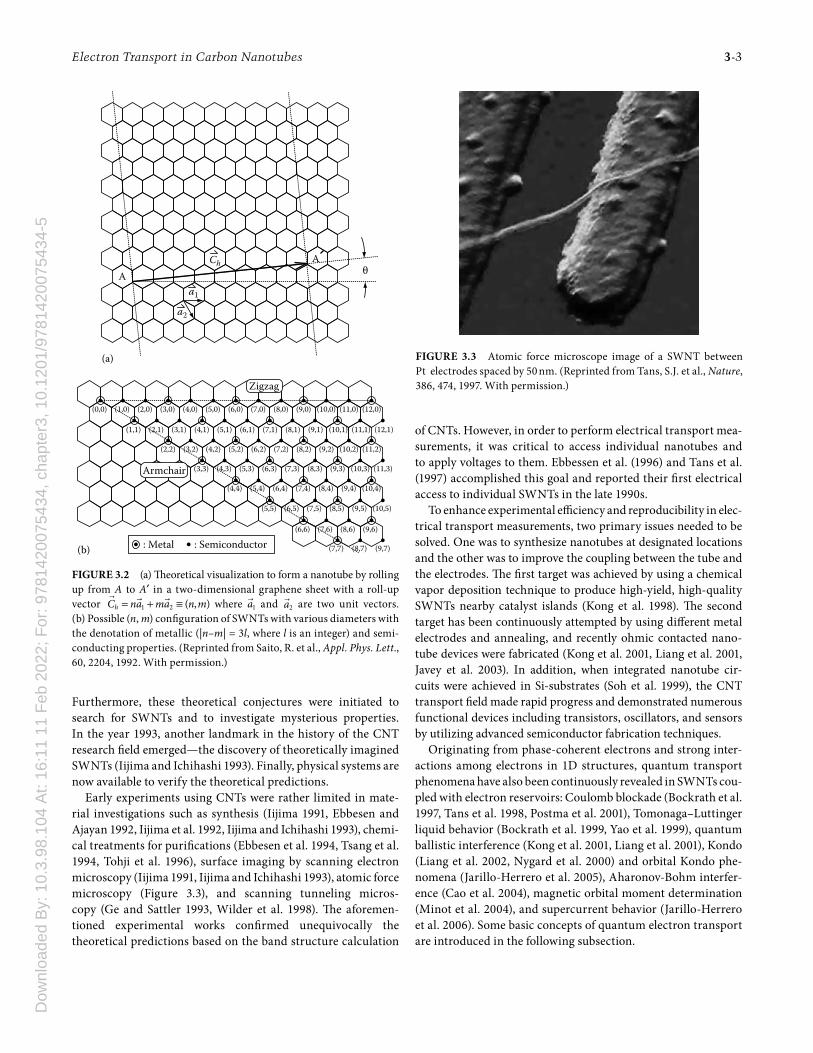
Early experiments using CNTs were rather limited in mate-rial investigations such as synthesis (Iijima 1991, Ebbesen and Ajayan 1992, Iijima et al. 1992, Iijima and Ichihashi 1993), chemi-cal treatments for purifi cations (Ebbesen et al. 1994, Tsang et al. 1994, Tohji et al. 1996), surface imaging by scanning electron microscopy (Iijima 1991, Iijima and Ichihashi 1993), atomic force microscopy (Figure 3.3), and scanning tunneling micros-copy (Ge and Sattler 1993, Wilder et al. 1998). Th e aforemen-tioned experimental works confi rmed unequivocally the theoretical predictions based on the band structure calculation
of CNTs. However, in order to perform electrical transport mea-surements, it was critical to access individual nanotubes and to apply voltages to them. Ebbessen et al. (1996) and Tans et al. (1997) accomplished this goal and reported their fi rst electrical access to individual SWNTs in the late 1990s.
To enhance experimental effi ciency and reproducibility in elec-trical transport measurements, two primary issues needed to be solved. One was to synthesize nanotubes at designated locations and the other was to improve the coupling between the tube and the electrodes. Th e fi rst target was achieved by using a chemical vapor deposition technique to produce high-yield, high-quality SWNTs nearby catalyst islands (Kong et al. 1998). Th e second target has been continuously attempted by using diff erent metal electrodes and annealing, and recently ohmic contacted nano-tube devices were fabricated (Kong et al. 2001, Liang et al. 2001, Javey et al. 2003). In addition, when integrated nanotube cir-cuits were achieved in Si-substrates (Soh et al. 1999), the CNT transport fi eld made rapid progress and demonstrated numerous functional devices including transistors, oscillators, and sensors by utilizing advanced semiconductor fabrication techniques.
Originating from phase-coherent electrons and strong inter-actions among electrons in 1D structures, quantum transport phenomena have also been continuously revealed in SWNTs cou-pled with electron reservoirs: Coulomb blockade (Bockrath et al. 1997, Tans et al. 1998, Postma et al. 2001), Tomonaga–Luttinger liquid behavior (Bockrath et al. 1999, Yao et al. 1999), quantum ballistic interference (Kong et al. 2001, Liang et al. 2001), Kondo (Liang et al. 2002, Nygard et al. 2000) and orbital Kondo phe-nomena (Jarillo-Herrero et al. 2005), Aharonov-Bohm interfer-ence (Cao et al. 2004), magnetic orbital moment determination (Minot et al. 2004), and supercurrent behavior (Jarillo-Herrero et al. 2006). Some basic concepts of quantum electron transport are introduced in the following subsection.
(a)
(0,0) (1,0)
(1,1)
(2,2)
(3,3)
(4,4)
(5,5)
(6,6)
(7,7) (8,7) (9,7)
(7,6) (8,6) (9,6)
(6,5) (7,5) (8,5) (9,5) (10,5)
(5,4) (6,4) (7,4) (8,4) (9,4) (10,4)
(4,3) (5,3) (6,3) (7,3) (8,3) (9,3) (10,3) (11,3)
(3,2) (4,2) (5,2) (6,2) (7,2) (8,2) (9,2) (10,2) (11,2)
(2,1) (3,1) (4,1) (5,1) (6,1) (7,1) (8,1) (9,1) (10,1) (11,1) (12,1)
(2,0) (3,0) (4,0) (5,0) (6,0) (7,0) (8,0) (9,0) (10,0) (11,0) (12,0)
(b)
Armchair
Zigzag
θAACh
: Metal : Semiconductor
a1
a2
FIGURE 3.2 (a) Th eoretical visualization to form a nanotube by rolling up from A to A′ in a two-dimensional graphene sheet with a roll-up vector = + ≡
� � �1 2 ( , )hC na ma n m where
�1a and
�2a are two unit vectors.
(b) Possible (n, m) confi guration of SWNTs with various diameters with the denotation of metallic (|n–m| = 3l, where l is an integer) and semi-conducting properties. (Reprinted from Saito, R. et al., Appl. Phys. Lett., 60, 2204, 1992. With permission.)
FIGURE 3.3 Atomic force microscope image of a SWNT between Pt electrodes spaced by 50 nm. (Reprinted from Tans, S.J. et al., Nature, 386, 474, 1997. With permission.)
Dow
nloa
ded
By:
10.
3.98
.104
At:
16:1
1 11
Feb
202
2; F
or: 9
7814
2007
5434
, cha
pter
3, 1
0.12
01/9
7814
2007
5434
-53-4 Handbook of Nanophysics: Nanotubes and Nanowires
3.2.2 Electron Transport
Mesoscopic systems refer to materials whose physical dimen-sions typically span from millimeters to nanometers. A SWNT is a representative mesoscopic system. Rigorously, a SWNT is an ideal 1D system since its Fermi wavelength λF is shorter than a longitudinal SWNT length, L. λF is a wavelength of carriers at Fermi energy (EF) level about 0.8 nm, and it is an important quantity since the majority of carriers are electrons near EF. In such low-dimensional systems, subtle and sophisticated features appear that are deeply rooted in quantum mechanics and tightly associated with many-body interactions.
Discerned from their classical counterpart, quantum transport properties refl ect unique traits of coherence and quantization in the system. Quantum transport is classifi ed into several regimes primarily by relevant lengthscale comparison. Th ese transport divisions are crucial in understanding transport properties in each regime. Besides λF, other relevant characteristic lengths are defi ned for classifi ed transport regimes: (1) mean free path, lmfp, (2) thermal diff usion length, lT, and (3) phase coherence length, lϕ.
3.2.2.1 Mean Free Path lmfp
Th e mean free path, as the name indicates, is the average dis-tance in which particles can move freely. Major sources to inhibit free motions of electrons are scatterers such as defects, impurities, or grain boundaries. Elastic scattering does not con-serve momentum but energy, while inelastic scattering changes both momentum and energy of incident particles. Th us, mean free paths due to elastic and inelastic scattering should be diff er-entiated accordingly, although generally, lmfp refers to the elastic mean free path. In semiconductors, lmfp is closely related to the mobility of carriers, and in metals lmfp is much longer than λF. As lmfp becomes comparable to λF, systems with such lmfp are called in the dirty limit.
3.2.2.2 Thermal Diffusion Length lT
At nonzero temperatures, electron wavepackets have an energy width of about kBT where kB is the Boltzmann’s constant and T is the temperature. Th is energy uncertainty induces diff usion in time. lT is a characteristic length of diff usion process due to thermal energy.
3.2.2.3 Phase Coherence Length lϕ
Within lϕ, particles preserve their phase. Dynamical interac-tions including mutual Coulomb interactions among electrons and electron-phonon interactions disturb phase coherence. Th erefore, this length is important to determine whether quan-tum interference eff ects from phase coherent sources can be detectable or not in systems.
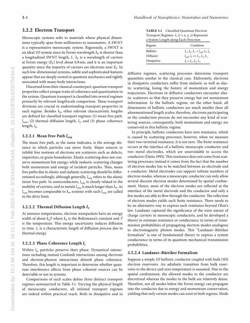
Comparisons of such scales defi ne three distinct transport regimes summarized in Table 3.1. Varying the physical length of mesoscopic conductors, all enlisted transport regimes are indeed within practical reach. Both in dissipative and in
diff usive regimes, scattering processes determine transport quantities similar to the classical case. Elaborately, electrons in dissipative conductors suff er from inelastic as well as elas-tic scattering, losing the history of momentum and energy trajectories. Electrons in diff usive conductors encounter elas-tic scatterers so that they preserve energy but not momentum information. In the ballistic regime, on the other hand, all dimensions of ballistic conductors are much smaller than all aforementioned length scales; therefore, electrons participating in the conduction process do not encounter any kind of scat-tering sources, consequently, both momentum and energy are conserved in this ballistic regime.
In principle, ballistic conductors have zero resistance, which is caused by scattering processes; however, when we measure their two-terminal resistance, it is not zero. Th e fi nite resistance occurs at the interface of a ballistic mesoscopic conductor and two metal electrodes, which are unavoidable to access the conductor (Datta 1995). Th is resistance does not come from scat-tering processes; instead it comes from the fact that the number of electron modes has to be matched between an electrode and a conductor. Metal electrodes can support infi nite numbers of electron modes, whereas a mesoscopic conductor can only allow several discrete electron modes determined by spatial confi ne-ment. Hence, most of the electron modes are refl ected at the interface of the metal electrode and the conductor and only a few modes are able to fl ow through the conductor. Th e refl ection of electron modes yields such fi nite resistance. Th ere needs to be an alternative way to express such resistance beyond Ohm’s law. Landauer captured the signifi cance of the wave nature of charge carriers in mesoscopic conductors, and he developed a theory to estimate resistance or conductance in terms of trans-mission probabilities of propagating electron modes analogous to electromagnetic photon modes. Th is “Landauer–Büttiker formalism” is one of fundamental theory to express a system conductance in terms of its quantum mechanical transmission probabilities.
3.2.2.4 Landauer–Büttiker Formalism
Suppose a simple 1D ballistic conductor coupled with bulk (3D) electron reservoirs. An adiabatic transition from bulk reser-voirs to the device and zero temperature is assumed. Due to the spatial confi nement, the allowed modes in the conductor are discretized whereas the modes in the bulk are relatively dense. Th erefore, not all modes below the Fermi energy can propagate into the conductor due to energy and momentum conservation, yielding that only certain modes can exist in both regions. Mode
TABLE 3.1 Classifi ed Quantum Electron Transport Regimes. Li (i = x, y, z) Represent a System Length along Each DirectionRegime Condition
Ballistic Lx, Ly, Lz < lmpf, lT, lϕDiff usive lmpf, lT << Lx, Ly, Lz
Dissipative lϕ < Lx, Ly, Lz
Dow
nloa
ded
By:
10.
3.98
.104
At:
16:1
1 11
Feb
202
2; F
or: 9
7814
2007
5434
, cha
pter
3, 1
0.12
01/9
7814
2007
5434
-5Electron Transport in Carbon Nanotubes 3-5
refl ection at the interface of two dissimilar materials causes fi nite conductance even with a ballistic conductor. Sometimes this fi nite resistance is called “contact resistance.” In the simplest case, only one channel in the conductor exists. Th e current I across the conductor with the applied bias voltage V is derived by
defi nition from +
= ρ∫F
Fg( ) ( )d
E eV
EI e E v E E with energy-dependent
density of states ρ, group velocity vg, and Fermi energy EF. Th e
density of states ρ in 1D is written as g
12 ( )v E
ρ =π� . Note that
in 1D, there is a magic cancellation of the velocity component, yielding the product of ρ and vg is constant 1/h. Hence, the cur-rent including spin degeneracy (a factor of 2) is
F
F
2
Q2 d 2
E eV
E
eI e E V G Vh h
+
= = ≡∫
where GQ is denoted as a spin-degenerate quantum unit of conductance when the mode is completely transmitting. If par-tial transmission occurs with a probability τ, the conductance becomes GQτ. Straightforwardly, this scheme can be extended to multi-mode channels whose individual transmission probabil-ity is τi, where the conductance G is summed over all modes,
= τ∑Q ii
G G , known as the “Landauer formula” (Datta 1995,
Imry and Landauer 1999). Since the hexagonal Brillouin zone of SWNTs contains two inequivalent K and K′ points, four bands degenerate at the same energy refl ecting the orbital and spin degeneracy. Th erefore, the ideal resistance of SWNTs is 2GQ = 4e2/h ∼ (6.45 kΩ)−1.
Besides conductance, noise (current fl uctuations) has also been actively studied in mesoscopic conductors (Blanter and Büttiker 2000). Th ere are several sources to generate current fl uctuations that are pronounced in mesoscopic conductors: internal microscopic random processes caused by thermal fl uctuations, scattering and tunneling, and quantum eff ects (Buckingham 1983, Blanter and Büttiker 2000). Noise theories have been developed intensively since its properties disclose correlations of charge carriers, scattering mechanisms, and quantum coherence, which are essential for understanding the electron transport properties especially in low-dimensional conductors. Recent endeavors in this direction are put into gain-ing a complete statistical analysis of charge transport under the name of “full counting statistics” (Levitov and Lesovik 1993, Levitov et al. 1996, Kindermann and Nazarov 2002, Nazarov et al. 2002). In the stochastic transport of quantized charged car-riers, nonequilibrium current fl uctuations are denoted as shot noise, the second moment of characteristic functions in the full counting statistics. What stimulates the advent of full count-ing statistics is the fact that higher moments provide additional information of systems beyond the fi rst moment, conductance. Th e focus of this chapter lies on two moments: conductance (the fi rst moment) and shot noise (the second moment) from which SWNTs’ electronic properties are quantifi ed.
3.2.3 Fermi-Liquid vs. Non-Fermi-Liquid Theories
Oft en, a single-particle picture describes macroscopic conduc-tors and their properties suffi ciently well with a valid justifi cation of eff ective screening. However, in lower dimensional systems as devices shrink down, screening among particles becomes insuffi -cient. Consequently, the many-body picture assumes a signifi cant role. In this section, two theoretical models are introduced: the Fermi-liquid (FL) theory and the Tomonaga–Luttinger liquid (TLL) theory. Th e former explains nominal features within a single parti-cle picture, whereas the latter explains the unique behaviors arising from many-body interactions particularly in 1D conductors.
3.2.3.1 Fermi-Liquid Theory
Th e FL theory is one of the successful solid-state frameworks to describe the physical properties of weakly interacting many-body condensed matter systems, such as the liquid state of 3He and conductivity in metals and semiconductors (Mahan 2007). In the FL system, there are still non-negligible interactions among particles. However, Landau ingeniously approached the FL system with a hypothesis that interactions are adiabatically switched on. Furthermore, he considered the long wavelength limit, namely, low energy excitations near the Fermi energy. He captured the idea that the interactions would modify the energy dispersion relation, consequently changing the mass of electrons in the system. By introducing the eff ective mass m*, which mani-fests the strength of mutual interactions, Landau established the FL theory within the single particle picture.
Th e essence of the FL theory is the existence of quasi-particles with the eff ective mass. Quasi-particles are low-lying elementary excitations consisting of electrons whose density fl uctuations arise from the particle interactions. Due to the fact that quasi-particles are formed from electrons, they possess fermionic nature such as obeying Pauli Exclusion Principle. Th e validity of the FL theory in higher dimensions relies on eff ective charge screening, which reduces the long-range Coulomb interactions among electrons. Th erefore, the FL theory works well to describe transport pro-cesses in systems whose interactions are short ranged and isotro-pic such as metals, semiconductors, and liquid 3He.
3.2.3.2 Tomonaga–Luttinger Liquid Theory
Th e successful FL theory fails in 1D. Th e breakdown of the FL theory in 1D conductors can be understood intuitively in terms of ineffi cient charge screening. Th e long-range Coulomb inter-actions survive among strongly correlated electrons. In 1D, any excitation at a particular site spreads over the whole lattice similar to the domino eff ect. Th is collectiveness is unique in 1D excita-tions, and Landau’s quasi-particles do not exist in 1D (Giamarchi 2004). A rigorous attempt to describe 1D electron gas systems is formulated as the TLL theory. Tomonaga and Luttinger came up with an exactly solvable model in 1D with insights that collective modes are bosonic in nature. By linearizing the dispersion rela-tion near the Fermi level, low energy properties of system can be extracted (Voit 1994, Giamarchi 2004).
Dow
nloa
ded
By:
10.
3.98
.104
At:
16:1
1 11
Feb
202
2; F
or: 9
7814
2007
5434
, cha
pter
3, 1
0.12
01/9
7814
2007
5434
-53-6 Handbook of Nanophysics: Nanotubes and Nanowires
Th e Fermi surface of 1D consists of two points at ±kF, where kF is the Fermi wavenumber. Particle-hole excitations in 1D are only possible near momentum q = 0 or q = 2kF near the Fermi points, whereas any q values below 2kF are allowed for particle-hole excitations in higher dimensions by conserving the energy and momentum. In the limit of q → 0 and low energy, the excita-tion spectrum is linear, resembling a phonon mode. Th is resem-blance hints that the Hamiltonian of 1D electron gas system can be derived by boson-like phonon displacements as a rather intuitive approach. Th e positive (negative) slope at kF(−kF) cor-responds to right (left ) moving channels. When interactions are renormalized in a system, the dimensionless quantity, the
TLL parameter g, is defi ned as
120
F1 Vg
v
−⎛ ⎞= +⎜ ⎟⎝ ⎠π�
, where V0 is the
interaction potential. It is a measure of competition between the interaction potential energy and the kinetic energy. In the absence of V0, g becomes 1, recovering the noninteracting Fermi gas system. On the other hand, V0 > �vF > 0 for a repulsive Coulomb interaction leads to g < 1. Th e stronger the interactions V0, the smaller the value of g. Note that g can also be greater than 1 if attractive Coulomb interactions are dominant among the particles. Th e TLL parameter g emerges in various 1D properties such as the fractional charge ge, the charge mode velocity vF/g, and the power-exponents of correlation functions.
As one specifi c example of 1D conductors, metallic SWNTs have been predicted as the TLL system (Egger and Gogolin 1997, Kane et al. 1997). Th e transport properties in the tun-neling regime, where tubes are isolated from metal reservoirs, exhibited the TLL features as the power-scaling conductance by means of the bias voltage and the temperatures (Bockrath et al. 1999). Th is nonlinear behavior certainly cannot be explained by a noninteracting single-particle picture. Recently, the spectral function from SWNT mats was obtained from angle-integrated photoemission measurements, which was claimed as the direct observation of the TLL features in SWNTs (Ishii et al. 2003).
Th e TLL parameter g for the SWNT is
12 2
S
F
81 lne Rgv R
−⎛ ⎞⎛ ⎞= + ⎜ ⎟⎜ ⎟⎝ ⎠π⎝ ⎠�
,
where RS is the screening length and R is the radius of the SWNT (Kane et al. 1997). Th e logarithmic dependence on RS/R explains that the value of g is rather insensitive to the actual value of RS (Kane et al. 1997), and the value falls between 0.2 and 0.3 with vF = 8 × 107 cm/s as RS/R > 4. Th e search of the TLL behavior in SWNTs is actively pursued since the strongly correlated SWNTs serve as a basic ingredient of quantum electron entanglers (Bena et al. 2002, Recher and Loss 2002, Bouchiat et al. 2003, Crépieux et al. 2003).
3.3 Electron Transport in Carbon Nanotubes
3.3.1 Synthesis and Device Fabrication
3.3.1.1 Synthesis
Th e discovery of MWNTs seems fortuitous in a carbon arc- discharge chamber that was designed to produce fullerenes
(Iijima 1991). Two years later, SWNTs were found by the same arc- discharge method except that catalytic components had been added into the chamber (Iijima and Ichihashi 1993). For a system-atic characterization of new materials toward functional device fabrication and quantum nature investigation, effi cient synthesis methods have been on demand that aim to isolate individual nan-otubes and grow specifi c types of SWNTs in a controllable way. Th ere are three major synthetic methods for growing SWNTs using catalytic nanoparticles: electric arc-discharge, laser ablation, and chemical vapor deposition (CVD). Among them, the CVD method has been superior in producing high-quality SWNTs.
Typically, the CVD chamber for growing SWNTs in the labo-ratory consists of a 1 in. diameter tube vessel inserted into a fur-nace, gas sources of CH4, H2 and Ar, a Si-substrate containing catalyst islands, and an exhaust system. Catalysts are essential for designating the location of SWNTs during growth. In 1999, Professor Dai’s group managed to synthesize a high-yield of SWNTs near the catalyst islands. Iron-based alumina-supported catalysts were under a carbon feedstock: 99.999% CH4 and H2 at the right concentration for 5–7 min at 900°C–1000°C followed by an Ar fl ush and a cool-down to room temperature (Kong et al. 1998). Th is work has advanced the SWNT research fi eld in which ballistic transport studies could be performed and prototypes of nanotube-electronics can be built.
Th e synthesis mechanism of SWNTs in the catalytic CVD method is associated with the details of nanoparticles. Recently, Li et al. (2001) have attempted to assess the role of catalysts and have shown that the diameter of SWNTs indeed closely links to the nanoparticle size based on statistical analysis. Th e report presents that the synthesis can be understood in three stages: First, nanoparticles as catalysts absorb decomposed carbon atoms from CH4 or other carbon feedstock in the CVD pro-cess. Second, the absorption of carbon atoms to nanoparticles continues until saturation. Once it reaches the saturation point, carbon atoms start to grow outward from the catalysts with a closed-end. Th ird, an excess carbon supply adds to the carbon precipitation on the surface, yielding fi nite-length nanotubes in the end. It is reasonable, therefore, that the SWNT diame-ter would be determined by the nanoparticle size as the initial basis. Although Li et al. (2001) provided valuable information as to the microscopic level of understanding of the synthesis in the catalytic CVD process, the complete controllability to produce tailor-made SWNTs with an expected diameter, chirality (roll-up vector direction), length, position, and orientation on demand is yet to be acquired, which is the present SWNT fabrication chal-lenge. Once this goal is achieved, it is not diffi cult to imagine that SWNTs would become widely utilized in various applications as electrical, chemical, mechanical, and optical components.
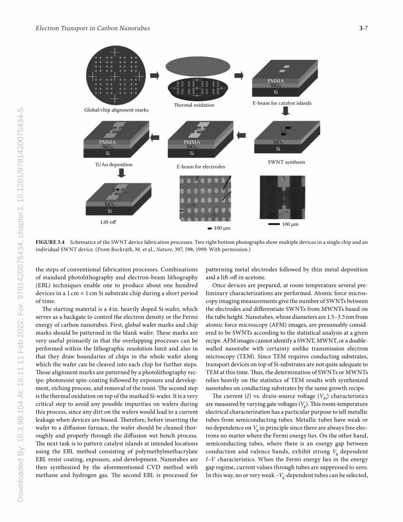
3.3.1.2 Device Fabrication
Th e confi guration of SWNT devices for electron transport mea-surements resembles conventional semiconductor fi eld-eff ect transistors, which have three terminals: source, drain, and gate. Th e fabrication goal is to produce three-terminal isolated SWNT nanotube devices on top of a Si-wafer. Figure 3.4 shows
Dow
nloa
ded
By:
10.
3.98
.104
At:
16:1
1 11
Feb
202
2; F
or: 9
7814
2007
5434
, cha
pter
3, 1
0.12
01/9
7814
2007
5434
-5Electron Transport in Carbon Nanotubes 3-7
the steps of conventional fabrication processes. Combinations of standard photolithography and electron-beam lithography (EBL) techniques enable one to produce about one hundred devices in a 1 cm × 1 cm Si substrate chip during a short period of time.
Th e starting material is a 4 in. heavily doped Si-wafer, which serves as a backgate to control the electron density or the Fermi energy of carbon nanotubes. First, global wafer marks and chip marks should be patterned in the blank wafer. Th ese marks are very useful primarily in that the overlapping processes can be performed within the lithographic resolution limit and also in that they draw boundaries of chips in the whole wafer along which the wafer can be cleaved into each chip for further steps. Th ose alignment marks are patterned by a photolithography rec-ipe: photoresist spin-coating followed by exposure and develop-ment, etching process, and removal of the resist. Th e second step is the thermal oxidation on top of the marked Si-wafer. It is a very critical step to avoid any possible impurities on wafers during this process, since any dirt on the wafers would lead to a current leakage when devices are biased. Th erefore, before inserting the wafer to a diff usion furnace, the wafer should be cleaned thor-oughly and properly through the diff usion wet bench process. Th e next task is to pattern catalyst islands at intended locations using the EBL method consisting of polymethylmethacrylate EBL resist coating, exposure, and development. Nanotubes are then synthesized by the aforementioned CVD method with methane and hydrogen gas. Th e second EBL is processed for
patterning metal electrodes followed by thin metal deposition and a lift -off in acetone.
Once devices are prepared, at room temperature several pre-liminary characterizations are performed. Atomic force micros-copy imaging measurements give the number of SWNTs between the electrodes and diff erentiate SWNTs from MWNTs based on the tube height. Nanotubes, whose diameters are 1.5–3.5 nm from atomic force microscopy (AFM) images, are presumably consid-ered to be SWNTs according to the statistical analysis at a given recipe. AFM images cannot identify a SWNT, MWNT, or a double-walled nanotube with certainty unlike transmission electron microscopy (TEM). Since TEM requires conducting substrates, transport devices on top of Si-substrates are not quite adequate to TEM at this time. Th us, the determination of SWNTs or MWNTs relies heavily on the statistics of TEM results with synthesized nanotubes on conducting substrates by the same growth recipe.
Th e current (I) vs. drain-source voltage (Vds) characteristics are measured by varying gate voltages (Vg). Th is room-temperature electrical characterization has a particular purpose to tell metallic tubes from semiconducting tubes. Metallic tubes have weak or no dependence on Vg in principle since there are always free elec-trons no matter where the Fermi energy lies. On the other hand, semiconducting tubes, where there is an energy gap between conduction and valence bands, exhibit strong Vg dependent I–V characteristics. When the Fermi energy lies in the energy gap regime, current values through tubes are suppressed to zero. In this way, no or very weak −Vg-dependent tubes can be selected,
Lift-off
Ti/Au deposition
Global/chip alignment marksThermal oxidation E-beam for catalyst islands
SWNT synthesisE-beam for electrodes
100 μm100 μm
SiO2Si
SiO2PMMA
SiSiO2
PMMA
Si
SiO2PMMA
Si
SiO2Si
FIGURE 3.4 Schematics of the SWNT device fabrication processes. Two right bottom photographs show multiple devices in a single chip and an individual SWNT device. (From Bockrath, M. et al., Nature, 397, 598, 1999. With permission.)
Dow
nloa
ded
By:
10.
3.98
.104
At:
16:1
1 11
Feb
202
2; F
or: 9
7814
2007
5434
, cha
pter
3, 1
0.12
01/9
7814
2007
5434
-53-8 Handbook of Nanophysics: Nanotubes and Nanowires
and room-temperature characterization has also another pur-pose to identify the best and good ohmic contacted devices for low-temperature measurements.
Th e subsequent two sections describe low-temperature electron transport properties: diff erential conductance and low-frequency shot noise. Th e main discussion focuses on three-terminal metallic SWNT devices that are well contacted to electrodes. Th e device dimension is fi xed between 200 and 600 nm by a distance between two electrodes. Th e Ti/Au, Ti-only, and Pd metal elec-trodes are used, which feature low-resistance contacts. Metallic SWNTs are considered to have both the elastic and the inelastic mean free path at least on the order of microns at low tempera-tures. Th erefore, the electron transport within 200–600 nm-long SWNTs is believed to be ballistic, where quantum coherence is preserved inside (Kong et al. 2001, Liang et al. 2001).
3.3.2 Differential Conductance
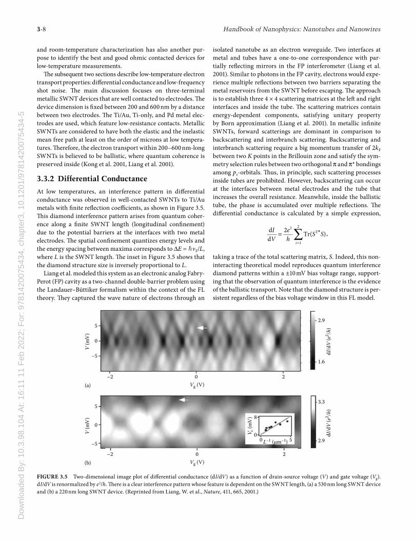
At low temperatures, an interference pattern in diff erential conductance was observed in well-contacted SWNTs to Ti/Au metals with fi nite refl ection coeffi cients, as shown in Figure 3.5. Th is diamond interference pattern arises from quantum coher-ence along a fi nite SWNT length (longitudinal confi nement) due to the potential barriers at the interfaces with two metal electrodes. Th e spatial confi nement quantizes energy levels and the energy spacing between maxima corresponds to ΔE = �vF/L, where L is the SWNT length. Th e inset in Figure 3.5 shows that the diamond structure size is inversely proportional to L.
Liang et al. modeled this system as an electronic analog Fabry-Perot (FP) cavity as a two-channel double-barrier problem using the Landauer–Büttiker formalism within the context of the FL theory. Th ey captured the wave nature of electrons through an
isolated nanotube as an electron waveguide. Two interfaces at metal and tubes have a one-to-one correspondence with par-tially refl ecting mirrors in the FP interferometer (Liang et al. 2001). Similar to photons in the FP cavity, electrons would expe-rience multiple refl ections between two barriers separating the metal reservoirs from the SWNT before escaping. Th e approach is to establish three 4 × 4 scattering matrices at the left and right interfaces and inside the tube. Th e scattering matrices contain energy-dependent components, satisfying unitary property by Born approximation (Liang et al. 2001). In metallic infi nite SWNTs, forward scatterings are dominant in comparison to backscattering and interbranch scattering. Backscattering and interbranch scattering require a big momentum transfer of 2kF between two K points in the Brillouin zone and satisfy the sym-metry selection rules between two orthogonal π and π* bondings among pz-orbitals. Th us, in principle, such scattering processes inside tubes are prohibited. However, backscattering can occur at the interfaces between metal electrodes and the tube that increases the overall resistance. Meanwhile, inside the ballistic tube, the phase is accumulated over multiple refl ections. Th e diff erential conductance is calculated by a simple expression,
22T
1
d 2 *Tr( )d
i
I e S SV h
=
= ∑ ,
taking a trace of the total scattering matrix, S. Indeed, this non-interacting theoretical model reproduces quantum interference diamond patterns within a ±10 mV bias voltage range, support-ing that the observation of quantum interference is the evidence of the ballistic transport. Note that the diamond structure is per-sistent regardless of the bias voltage window in this FL model.
–2
–5
0
5
(b)0
Vg (V)
L–1 (μm–1)
V (m
V)
V c (m
V)
2
00 5
8
–2
–5
0
5
(a)0
Vg (V)
V (m
V)
2
2.9
3.3
dI/d
V (e
2 /h)
1.6
2.9dI
/dV
(e2 /h
)
FIGURE 3.5 Two-dimensional image plot of diff erential conductance (dI/dV) as a function of drain-source voltage (V) and gate voltage (Vg). dI/ dV is renormalized by e2/h. Th ere is a clear interference pattern whose feature is dependent on the SWNT length, (a) a 530 nm long SWNT device and (b) a 220 nm long SWNT device. (Reprinted from Liang, W. et al., Nature, 411, 665, 2001.)
Dow
nloa
ded
By:
10.
3.98
.104
At:
16:1
1 11
Feb
202
2; F
or: 9
7814
2007
5434
, cha
pter
3, 1
0.12
01/9
7814
2007
5434
-5Electron Transport in Carbon Nanotubes 3-9
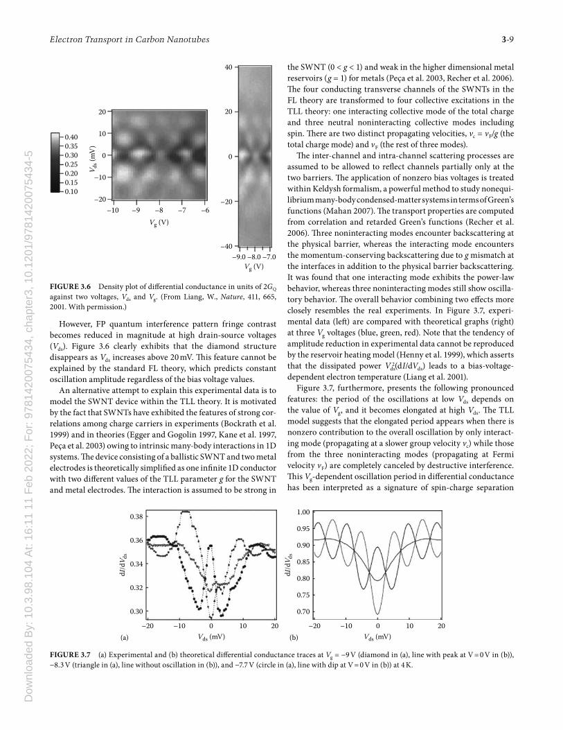
However, FP quantum interference pattern fringe contrast becomes reduced in magnitude at high drain-source voltages (Vds). Figure 3.6 clearly exhibits that the diamond structure disappears as Vds increases above 20 mV. Th is feature cannot be explained by the standard FL theory, which predicts constant oscillation amplitude regardless of the bias voltage values.
An alternative attempt to explain this experimental data is to model the SWNT device within the TLL theory. It is motivated by the fact that SWNTs have exhibited the features of strong cor-relations among charge carriers in experiments (Bockrath et al. 1999) and in theories (Egger and Gogolin 1997, Kane et al. 1997, Peça et al. 2003) owing to intrinsic many-body interactions in 1D systems. Th e device consisting of a ballistic SWNT and two metal electrodes is theoretically simplifi ed as one infi nite 1D conductor with two diff erent values of the TLL parameter g for the SWNT and metal electrodes. Th e interaction is assumed to be strong in
the SWNT (0 < g < 1) and weak in the higher dimensional metal reservoirs (g = 1) for metals (Peça et al. 2003, Recher et al. 2006). Th e four conducting transverse channels of the SWNTs in the FL theory are transformed to four collective excitations in the TLL theory: one interacting collective mode of the total charge and three neutral noninteracting collective modes including spin. Th ere are two distinct propagating velocities, vc = vF/g (the total charge mode) and vF (the rest of three modes).
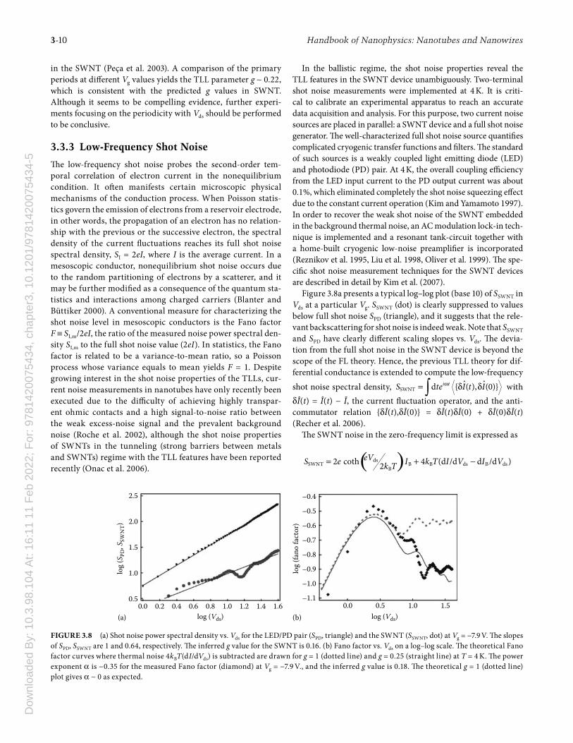
Th e inter-channel and intra-channel scattering processes are assumed to be allowed to refl ect channels partially only at the two barriers. Th e application of nonzero bias voltages is treated within Keldysh formalism, a powerful method to study nonequi-librium many-body condensed-matter systems in terms of Green’s functions (Mahan 2007). Th e transport properties are computed from correlation and retarded Green’s functions (Recher et al. 2006). Th ree noninteracting modes encounter backscattering at the physical barrier, whereas the interacting mode encounters the momentum-conserving backscattering due to g mismatch at the interfaces in addition to the physical barrier backscattering. It was found that one interacting mode exhibits the power-law behavior, whereas three noninteracting modes still show oscilla-tory behavior. Th e overall behavior combining two eff ects more closely resembles the real experiments. In Figure 3.7, experi-mental data (left ) are compared with theoretical graphs (right) at three Vg voltages (blue, green, red). Note that the tendency of amplitude reduction in experimental data cannot be reproduced by the reservoir heating model (Henny et al. 1999), which asserts that the dissipated power Vds
2(dI/dVds) leads to a bias-voltage-dependent electron temperature (Liang et al. 2001).
Figure 3.7, furthermore, presents the following pronounced features: the period of the oscillations at low Vds depends on the value of Vg, and it becomes elongated at high Vds. Th e TLL model suggests that the elongated period appears when there is nonzero contribution to the overall oscillation by only interact-ing mode (propagating at a slower group velocity vc) while those from the three noninteracting modes (propagating at Fermi velocity vF) are completely canceled by destructive interference. Th is Vg-dependent oscillation period in diff erential conductance has been interpreted as a signature of spin-charge separation
–20(a)
0.30
0.32
0.34
0.36
0.38
–10 0Vds (mV)
dI/d
V ds
10 20 –20(b)
0.70
0.75
0.80
0.85
0.90
0.95
1.00
–10 0Vds (mV)
dI/d
V ds
10 20
FIGURE 3.7 (a) Experimental and (b) theoretical diff erential conductance traces at Vg = −9 V (diamond in (a), line with peak at V = 0 V in (b)), −8.3 V (triangle in (a), line without oscillation in (b)), and −7.7 V (circle in (a), line with dip at V = 0 V in (b)) at 4 K.
0.10–20–20
0
20
40
–40
–10 –9 –8Vg (V)
Vg (V)
–7
–7.0–8.0–9.0
–6
–10
0
10
20
0.150.20 V d
s (m
V)
0.250.300.350.40
FIGURE 3.6 Density plot of diff erential conductance in units of 2GQ against two voltages, Vds and Vg. (From Liang, W., Nature, 411, 665, 2001. With permission.)
Dow
nloa
ded
By:
10.
3.98
.104
At:
16:1
1 11
Feb
202
2; F
or: 9
7814
2007
5434
, cha
pter
3, 1
0.12
01/9
7814
2007
5434
-53-10 Handbook of Nanophysics: Nanotubes and Nanowires
in the SWNT (Peça et al. 2003). A comparison of the primary periods at diff erent Vg values yields the TLL parameter g ∼ 0.22, which is consistent with the predicted g values in SWNT. Although it seems to be compelling evidence, further experi-ments focusing on the periodicity with Vds should be performed to be conclusive.
3.3.3 Low-Frequency Shot Noise
Th e low-frequency shot noise probes the second-order tem-poral correlation of electron current in the nonequilibrium condition. It oft en manifests certain microscopic physical mechanisms of the conduction process. When Poisson statis-tics govern the emission of electrons from a reservoir electrode, in other words, the propagation of an electron has no relation-ship with the previous or the successive electron, the spectral density of the current fl uctuations reaches its full shot noise spectral density, SI = 2eI, where I is the average current. In a mesoscopic conductor, nonequilibrium shot noise occurs due to the random partitioning of electrons by a scatterer, and it may be further modifi ed as a consequence of the quantum sta-tistics and interactions among charged carriers (Blanter and Büttiker 2000). A conventional measure for characterizing the shot noise level in mesoscopic conductors is the Fano factor F ≡ SI,m/2eI, the ratio of the measured noise power spectral den-sity SI,m to the full shot noise value (2eI). In statistics, the Fano factor is related to be a variance-to-mean ratio, so a Poisson process whose variance equals to mean yields F = 1. Despite growing interest in the shot noise properties of the TLLs, cur-rent noise measurements in nanotubes have only recently been executed due to the diffi culty of achieving highly transpar-ent ohmic contacts and a high signal-to-noise ratio between the weak excess-noise signal and the prevalent background noise (Roche et al. 2002), although the shot noise properties of SWNTs in the tunneling (strong barriers between metals and SWNTs) regime with the TLL features have been reported recently (Onac et al. 2006).
In the ballistic regime, the shot noise properties reveal the TLL features in the SWNT device unambiguously. Two-terminal shot noise measurements were implemented at 4 K. It is criti-cal to calibrate an experimental apparatus to reach an accurate data acquisition and analysis. For this purpose, two current noise sources are placed in parallel: a SWNT device and a full shot noise generator. Th e well-characterized full shot noise source quantifi es complicated cryogenic transfer functions and fi lters. Th e standard of such sources is a weakly coupled light emitting diode (LED) and photodiode (PD) pair. At 4 K, the overall coupling effi ciency from the LED input current to the PD output current was about 0.1%, which eliminated completely the shot noise squeezing eff ect due to the constant current operation (Kim and Yamamoto 1997). In order to recover the weak shot noise of the SWNT embedded in the background thermal noise, an AC modulation lock-in tech-nique is implemented and a resonant tank-circuit together with a home-built cryogenic low-noise preamplifi er is incorporated (Reznikov et al. 1995, Liu et al. 1998, Oliver et al. 1999). Th e spe-cifi c shot noise measurement techniques for the SWNT devices are described in detail by Kim et al. (2007).
Figure 3.8a presents a typical log–log plot (base 10) of SSWNT in Vds at a particular Vg. SSWNT (dot) is clearly suppressed to values below full shot noise SPD (triangle), and it suggests that the rele-vant backscattering for shot noise is indeed weak. Note that SSWNT and SPD have clearly diff erent scaling slopes vs. Vds. Th e devia-tion from the full shot noise in the SWNT device is beyond the scope of the FL theory. Hence, the previous TLL theory for dif-ferential conductance is extended to compute the low-frequency
shot noise spectral density, ω= δ δ∫SWNTˆ ˆd { ( ), (0)}i tS te I t I with
δÎ(t) = Î(t) − Ī, the current fl uctuation operator, and the anti-commutator relation {δÎ(t),δÎ(0)} = δÎ(t)δÎ(0) + δÎ(0)δÎ(t) (Recher et al. 2006).
Th e SWNT noise in the zero-frequency limit is expressed as
( )= + −dsSWNT B B ds B ds
B2 coth 4 (d /d d /d )2
eVS e I k T I V I Vk T
0.0(a)
0.5
1.0
1.5
2.0
2.5
0.40.2 0.6 0.8log (Vds)
log
(SPD
, SSW
NT)
1.21.0 1.61.4(b)
–1.1
–1.0
–0.9
–0.8
–0.7
–0.6
–0.5
–0.4
0.0 0.5log (Vds)
log
(fano
fact
or)
1.0 1.5
FIGURE 3.8 (a) Shot noise power spectral density vs. Vds for the LED/PD pair (SPD, triangle) and the SWNT (SSWNT, dot) at Vg = −7.9 V. Th e slopes of SPD, SSWNT are 1 and 0.64, respectively. Th e inferred g value for the SWNT is 0.16. (b) Fano factor vs. Vds on a log–log scale. Th e theoretical Fano factor curves where thermal noise 4kBT(dI/dVds) is subtracted are drawn for g = 1 (dotted line) and g = 0.25 (straight line) at T = 4 K. Th e power exponent α is −0.35 for the measured Fano factor (diamond) at Vg = −7.9 V., and the inferred g value is 0.18. Th e theoretical g = 1 (dotted line) plot gives α ∼ 0 as expected.
Dow
nloa
ded
By:
10.
3.98
.104
At:
16:1
1 11
Feb
202
2; F
or: 9
7814
2007
5434
, cha
pter
3, 1
0.12
01/9
7814
2007
5434
-5Electron Transport in Carbon Nanotubes 3-11
where IB is the backscattered current. In the limit of eVds > kBT, the SWNT noise spectral power density becomes simplifi ed as SSWNT = 2eIB. Th e asymptotic behavior of IB follows the power-law scaling 1
B ds~I V +α with α = −(1/2) (1 − g)/(1 + g). Th e power exponent α is uniquely determined by the TLL parameter g.
Th e experimental Fano factor F(Vds) is displayed on a log–log (base 10) scale in Figure 3.8b. Th e TLL model predicts that at low bias voltages eVds < kBT < �/2gtF, experimental Fano factor Fexp
is proportional to Vds if we subtract the thermal noise compo-nent. In addition, the slope between Fexp and Vds is insensitive to g-values in the region of log(Vds) < log (�/2gtF) ∼ 0.47. On the other hand, if eVds > �/2gtF, a power-law F ∼ Vds
α is expected by assumption that the backscattered current is smaller than the ideal current 2GQVds. A linear regression analysis of the Fano fac-tor F with Vds in this region, therefore, is another means to obtain the g value. Th e Fano factors F for g = 0.25 (red) and g = 1 (yellow) are displayed on a log–log scale in Figure 3.8b. Th e experimen-tal data (diamonds) agree well with the theoretical Fano factor of g = 0.25. Th e stiff er slope (α) corresponds to a stronger electron–electron interaction. Th e measured exponent α and inferred g values from the spectral density and the Fano factor from four diff erent devices with various metal electrodes (Ti/Au, Ti-only, Pd) show similar statistics of α ∼ −0.31 ± 0.047 and g ∼ 0.26 ± 0.071 as derived from several Vg values for each sample. Many-body TLL behavior in the ballistic SWNT is clearly probed in the shot noise properties.
3.4 Summary
Th e electron transport properties of SWNTs are discussed based on experimental results and theoretical models. Th e discussion started from the discovery of carbon nanotubes and the history of their research fi eld with a focus on the electron transport area. Th e noninteracting FL and interacting TLL theories, which have been used widely for bulk and 1D systems respectively, are briefl y introduced as background knowledge. Th e ballistic transport regime is clearly defi ned, in which no inelastic and elastic scat-tering occurs, consequently quantum coherence is preserved.
A metallic SWNT is a model system to investigate ballistic transport properties in 1D owing to quantum many-body inter-actions. Th e diff erential conductance and the shot noise have been measured, and their experimental signatures are examined by the FL and the TLL theoretical frameworks. It is clear that quantum coherent properties manifest as an interference pat-tern in diff erential conductance, and unique power-law scaling behavior quantifi es correlations among charge carriers. A non-interacting picture may describe conductance data in the low bias regime; however, it fails to explain the high-energy regions of experimental data. Th e TLL theory has explained the qualita-tive trend of conductance as a function of the drain-source volt-age. In addition, it has captured the quantitative information of the strong electron–electron interactions both in conductance and the shot noise quantities. Th e strength of the interactions is parameterized by the TLL parameter, g, which has been obtained
from the conductance period at various Vg and power-law scal-ing exponents from both shot noise and the Fano factor. Th e search of many-body collective phenomena in SWNT devices would provide fundamental physical knowledge in 1D electron transport properties.
3.5 Future Perspective
CNTs have been greatly infl uential in numerous areas based on extraordinary properties in physics, chemistry, chemical engi-neering, mechanical engineering, electrical engineering, and more. In particular, conductance and shot noise properties are important because they would ultimately provide the limit-ing performance of electronic devices. Th is chapter focuses on the early work of this property on a particular type of carbon nanotubes: metallic SWNTs. However, there has been growing interest with regard to these current fl uctuations of diverse SWNT device structures. Th e knowledge acquired from SWNTs can certainly be transferred to other 1D systems and also carbon nanotube mother material including fullerene and graphene (Bréchignac et al. 2007, Dupas et al. 2007). At present, an experi-mental investigation on graphene is indeed very exciting and progressively moving forward in comparison with carbon nano-tube properties. Th erefore, this fi eld will continue to deepen low-dimensional physical knowledge and to build pragmatic devices and systems that can impact everyday lives of human beings (Baughman et al. 2002).
References
Baughman, R. H., Zakhidov, A. A., and de Heer, W. A. 2002. Carbon nanotubes—Th e route toward applications. Science 297: 787–792.
Bena, C., Vishveshware, S., Balents, L., and Fisher, M. P. A. 2002. Quantum entanglement in carbon nanotubes. Phys. Rev. Lett. 89: 037901.
Blanter, Ya. M. and Büttiker, M. 2000. Shot noise in mesoscopic conductors. Phys. Rep. 336: 1–166.
Bockrath, M., Cobden, D. H., McEuen, P. L. et al. 1997. Single-electron transport in ropes of carbon nanotubes. Science 275: 1922–1925.
Bockrath, M., Cobden, D. H., Lu, J. et al. 1999. Luttinger-liquid behavior in carbon nanotubes. Nature 397: 598–601.
Bouchiat, V., Chtchelkatchev, N., Feinberg, D., Lesovik, G. B., Martin, T., and Torres, J. 2003. Single-walled carbon nanotube-superconductor entangler: Noise correlations and Einstein-Podolsky-Rosen states. Nanotechnology 14: 77–85.
Bréchignac, C., Houdy, P., and Lahmani, M. 2007. Nanomaterials and Nanochemistry. Berlin/Heidelberg, Germany: Springer.
Buckingham, M. J. 1983. Noise in Electronic Devices and Systems. New York: John Wiley & Sons.
Cao, J., Wang, Q., Rolandi, M., and Dai, H. 2004. Aharonov-Bohm interference and beating in single-walled carbon-nanotube interferometers. Phys. Rev. Lett. 93: 216803.
Dow
nloa
ded
By:
10.
3.98
.104
At:
16:1
1 11
Feb
202
2; F
or: 9
7814
2007
5434
, cha
pter
3, 1
0.12
01/9
7814
2007
5434
-53-12 Handbook of Nanophysics: Nanotubes and Nanowires
Crépieux, A., Guyon, R., Devillard, P., and Martin, T. 2003. Electron injection in a nanotube: Noise correlations and entanglement. Phys. Rev. B 67: 205408.
Datta, S. 1995. Electronic Transport in Mesoscopic Systems. Cambridge, U.K.: Cambridge University Press.
Dekker, C. 1999. Carbon nanotubes as molecular quantum wires. Phys. Today 5: 22–28.
Dupas, C., Houdy, P., and Lahmani, M. 2007. Nanoscience—Nanotechnologies and Nanophysics. Berlin/Heidelberg, Germany: Springer.
Ebbesen, T. W. and Ajayan, P. M. 1992. Large-scale synthesis of carbon nanotubes. Nature 358: 220–222.
Ebbesen, T. W., Ajayan, P. M., Hiura, H., and Tanigaki, K. 1994. Purifi cation of nanotubes. Nature 367: 519.
Ebbesen, T. W., Lezec, T. H., Hiura, H., Bennett, J. W., Ghaemi, H. F., and Th io, T. 1996. Electrical conductivity of individual car-bon nanotubes. Nature 382: 54–56.
Egger, R. and Gogolin, A. O. 1997. Eff ective low-energy the-ory for correlated carbon nanotubes. Phys. Rev. Lett. 79: 5082–5085.
Ge, M. and Sattler, K. 1993. Vapor-condensation generation and {STM} analysis of fullerene tubes. Science 260: 515–518.
Giamarchi, T. 2004. Quantum Physics in One Dimension. Oxford, U.K.: Oxford University Press.
Harris, P. J. F. 1999. Carbon Nanotubes and Related Structures: New Materials for the Twenty-First Century. Cambridge, U.K.: Cambridge University Press.
Henny, M., Oberholzer, S., Strunk, C., and Schonenberger, C. 1999. 1/3-Shot-noise suppression in diff usive nanowires. Phys. Rev. B 59: 2871–2880.
Iijima, S. 1991. Helical microtubules of graphitic carbon. Nature 354: 56–58.
Iijima, S. and Ichihashi, T. 1993. Single-shell carbon nanotubes of 1-nm diameter. Nature 363: 603–605.
Iijima, S., Ichihashi, T., and Ando, Y. 1992. Pentagons, heptagons and negative curvature in graphite microtubule growth. Nature 356: 776–778.
Imry, Y. and Landauer, R. 1999. Conductance viewed as transmis-sion. Rev. Mod. Phys. 71: S306–S312.
Ishii, H., Kataura, H., Shiozawa, H. et al. 2003. Direct observation of Tomonaga-Luttinger-liquid state in carbon nanotubes at low temperatures. Nature 426: 540–544.
Jarillo-Herrero, P., Kong, J., Van der Zant, H. S. J. et al. 2005. Orbital Kondo eff ect in carbon nanotubes. Nature 434: 484–488.
Jarillo-Herrero, P., van Dam, J., and Kouwenhoven, L. 2006. Quantum supercurrent transistors in carbon nanotubes. Nature 439: 953–956.
Javey, A., Guo, J., Paulsson, M. et al. 2004. High-fi eld quasi bal-listic transport in short carbon nanotubes. Phys. Rev. Lett. 92: 106804.
Javey, A., Guo, J., Wang, Q., Lundstrom, M., and Dai, H. 2003. Ballistic carbon nanotube fi eld-eff ect transistors. Nature 424: 654–657.
Jorio, A., Dresselhaus, G., and Dresselhaus, M. S. 2008. Carbon Nanotubes: Advanced Topics in the Synthesis, Structure, Properties and Applications. Berlin/Heidelberg, Germany: Springer.
Kane, C., Balents, L., and Fisher, M. P. A. 1997. Coulomb inter-actions and mesoscopic eff ects in carbon nanotubes. Phys. Rev. Lett. 79: 5086–5089.
Kim, J. and Yamamoto, Y. 1997. Th eory of noise in P-N junction light emitters. Phys. Rev. B 55: 9949–9959.
Kim, N. Y., Recher, P., Oliver, W. D., Yamamoto, Y., Kong, J., and Dai, H. 2007. Tomonaga-Luttinger liquid features in ballis-tic single-walled carbon nanotubes: Conductance and shot noise. Phys. Rev. Lett. 99: 036802.
Kindermann, M. and Nazarov, Yu. V. 2002 Full counting statis-tics in electric circuits. In Quantum Noise in Mesoscopic Physics, eds. Yu. V. Nazarov and Ya. M. Blanter, pp. 403–429. Dordrecht, the Netherlands: Kluwer Academic Publishers.
Kong, J., Soh, H. T., Cassell, A. M., Quate, C. F., and Dai, H. 1998. Synthesis of individual single-walled carbon nanotubes on patterned silicon wafers. Nature 395: 878–881.
Kong, J., Yenilmez, E., Tombler, T. W. et al. 2001. Quantum inter-ference and ballistic transmission in nanotube electron waveguides. Phys. Rev. Lett. 87: 106801.
Levitov, L. S., Lee, H., and Lesovik, G. B. 1996. Electron count-ing statistics and coherent states of electric current. J. Math. Phys. 37: 4845–4866.
Levitov, L. S. and Lesovik, G. B. 1993. Charge distribution in quantum shot noise. JETP Lett. 58: 230–235.
Li, Y., Kim, W., Zhang, Y., Rolandi, M., Wang, D., and Dai, H. 2001. Growth of single-walled carbon nanotubes from discrete catalytic nanoparticles of various sizes. J. Phys. Chem. B 105: 11424–11431.
Liang, W., Bockrath, M., Bozovic, D., Hafner, J. H., Tinkham, M., and Park, H. 2001. Fabry-Perot interference in a nanotube electron waveguide. Nature 411: 665–669.
Liang, W., Bockrath, M., and Park, H. 2002. Shell fi lling and exchange coupling in metallic single-walled carbon nano-tubes. Phys. Rev. Lett. 88: 126801.
Liu, R. C., Odom, B., Yamamoto, Y., and Tarucha, S. 1998. Quantum interference in electron collision. Nature 391: 263–265.
Mahan, G. D. 2007. Many-Particle Physics. New York: Springer.Minot, E. D., Yaish, Y., Sazonova, V., and McEuen, P. L. 2004.
Determination of electron orbital magnetic moments in carbon nanotubes. Nature 428: 536–539.
Mintmire, J. W., Dunlap, B. I., and White, C. T. 1992. Are fullerene tubules metallic? Phys. Rev. Lett. 68: 631–634.
Nazarov, Yu. V. and Bagrets, D. A. 2002. Circuit theory for full counting statistics in multiterminal circuits. Phys. Rev. Lett. 88: 196801.
Nygard, J., Cobden, D. H., and Lindelof, P. E. 2000. Kondo physics in carbon nanotubes. Nature 408: 342–346.
Dow
nloa
ded
By:
10.
3.98
.104
At:
16:1
1 11
Feb
202
2; F
or: 9
7814
2007
5434
, cha
pter
3, 1
0.12
01/9
7814
2007
5434
-5Electron Transport in Carbon Nanotubes 3-13
Oliver, W. D., Kim, J., Liu, R. C., and Yamamoto, Y. 1999. Hanbury Brown and Twiss-type experiment with electrons. Science 284: 299–302.
Onac, E., Balestro, F., Trauzettel, B., Lodewijk, C. F. J., and Kouwenhoven, L. P. 2006. Shot-noise detection in a carbon nanotube quantum dot. Phys. Rev. Lett. 96: 026803.
Park, J., Rosenblatt, S., Yaish, Y. et al. 2004. Electron-phonon scat-tering in metallic single-walled carbon nanotubes. Nano Lett. 4: 517–520.
Peça, C. S., Balents, L., and Wiese, K. J. 2003. Fabry-Perot inter-ference and spin fi ltering in carbon nanotubes. Phys. Rev. B 68: 205423.
Postma, H. W. Ch., Teepen, T, Yao, Z., Grifoni, M., and Dekker, C. 2001. Carbon nanotube single-electron transistors at room temperature. Science 293: 76–79.
Recher, P., Kim, N. Y., and Yamamoto, Y. 2006. Tomonaga-Luttinger liquid correlations and Fabry-Perot interference in conductance and fi nite-frequency shot noise in a single-walled carbon nanotube. Phys. Rev. B 74: 235438.
Recher, P. and Loss, D. 2002. Superconductor coupled to two Luttinger liquids as an Entangler for electron spins. Phys. Rev. B 65: 165327.
Roche, P.-E., Kociak, M., Gueron, S., Kasumov, A., Reulet, B., and Bouchiart, H. 2002. Very low shot noise in carbon nano-tubes. Euro. Phys. J. B 28: 217–222.
Reznikov, M., Heiblum, H., Shtrikman, H., and Mahalu, D. 1995. Temporal correlation of electrons: Suppression of shot noise in a ballistic quantum point contact. Phys. Rev. Lett. 75: 3340–3343.
Saito, R., Dresselhaus, G., and Dresselhaus, M. S. 1998. Physical Properties of Carbon Nanotubes. London, U.K.: Imperial College Press.
Saito, R., Fujita, M., Dresselhaus, G., and Dresselhaus, M. S. 1992. Electronic structure of chiral graphene tubules. Appl. Phys. Lett. 60: 2204–2206.
Soh, H. T., Quate, C. F., Morpurgo, A. F., Marcus, C. M., Kong, J., and Dai, H. 1999. Integrated nanotube circuits: Controlled growth and ohmic contacting of single-walled carbon nan-otubes. Appl. Phys. Lett. 75: 627–629.
Tans, S. J., Devoret, M. H., Dai, H. et al. 1997. Individual sin-gle-wall carbon nanotubes as quantum wires. Nature 386: 474–477.
Tans, S. J., Verschueren, A. R. M., and Dekker, C. 1998. Room-temperature transistor based on a single carbon nanotube. Nature 393: 49–52.
Tohji, K., Goto, T., Takahashi, H., Shinoda, Y., and Shimizu, N. 1996. Purifying single-walled nanotubes. Nature 383: 679.
Tsang, S. C., Chen, Y. K., Harris, P. J. F., and Green, M. L. H. 1994. A simple chemical method of opening and fi lling carbon nanotubes. Nature 372: 159–162.
Voit, J. 1994. One-dimensional Fermi liquids. Rep. Prog. Phys. 57: 977–1116.
Wallace, P. R. 1947. Th e band theory of graphite. Phys. Rev. 71: 622–634.
Wilder, J. W. G., Venema, L. C., Rinzler, A. G., Smalley, R. E., and Dekker, C. 1998. Electronic structure of atomically resolved carbon nanotubes. Nature 391: 59–52.
Yao, Z., Kane, C. L., and Dekker, C. 2000. High-fi eld electrical transport in single-wall carbon nanotubes. Phys. Rev. Lett. 84: 2941–2944.
Yao, Z., Postma, H. W. Ch., Balents, L., and Dekker, C. 1999. Carbon nanotube intramolecular junctions. Nature 402: 273–276.