Embed Size (px)
Citation preview

neel.c
nrs
.fr
highlights4


neel.c
nrs
.fr
highlights
Deuterated KDP crystals Optical measurement Epitaxy machine Superconducting C60
transitor4

DAte oF PuBLicAtioN: 2010
Director oF PuBLicAtioN Alain FoNTAiNE
eDitorLaurent LEVY
coPy eDitorSronald coX, Nora DEmPSEY
ProDuctioNNathalie BoUrGEAT-LAmi
DeSigN & LAyoutagence-connivence.fr
coPyrigHtS© cNrS Photothèque/Alexis chEZiErES© cNrS Photothèque/Emmanuel PErriN
PriNtiNg Press Vercors
Louis Néel,the founder of Grenoble’s
research centres.
2010, 40 years after
his Nobel prize, his heritage lives on...
“J’ai été précédé, au Xiie siècle,
par Pierre de maricourt, auteur en 1269 du premier
traité sérieux sur les aimants. En matière scientifique,
on a souvent des prédécesseurs beaucoup plus anciens
qu’on ne le pense.”
L. Néel, Stockholm, 1970”Je ne désirais
pas rester à Grenoble pour en faire le marche pied
d’une carrière parisienne, mais bien avec l’intention
de créer un centre de recherche suffisamment important
pour en retenir les cadres...”
L. NéelUn siècle de physique 1991

Editorial
in addition, in the core areas of our expertise - highly ranked by the recent AErES evaluation committee -
“highlights” 2010 features new breakthroughs for the Nanofab technology platform, automats for cryogenics
regulation, GaN quantum dots inserted in nanowires, permanent magnet microflux sources, a superconducting
single molecule transistor, together with leading research results in helium condensation in aerogels, quantum
phase-slips in a Josephson junction chain, radiative heat fluxes at sub-micron distances (greatly enhanced beyond
the classical Stefan-Boltzmann law), and not forgetting the always attractive thin-film diamond. recognized as
a wide bandgap semiconductor for several decades, diamond has now achieving unprecedented performance in
terms of hole mobility and yielded a Schottky diode with breakdown voltage surpassing the magic 10 kV threshold.
2010 is also the 40th anniversary of Louis Néel’s Nobel Prize in Physics. The Néel Institute is honoured to host the cel-
ebration ceremony, which will take place October 20th-21st as a major event of Grenoble’s annual “Science Festival”
for this year. For the organization of the commemoration, the Institute has received the valuable support of the City
of Grenoble and the CCSTI Cultural Centre, and the enthusiastic participation of Joseph Fourier University, Grenoble
Institute of Technology (INP), the CEA, the ESRF and the ILL, Grenoble Université EPCS and GIANT.
in 2011, a century after the discovery of superconductivity by Kamerlingh onnes in Leiden, we will take the
opportunity to celebrate the first French production of the cryogenic fluids hydrogen and helium in Grenoble,
initiated by Albert Lacaze and Louis Weil in the early 50s. Their work was the seed for the Grenoble area’s
exceptional concentration of academic and industrial expertise in cryogenics. over the last 60 years, the
synergy between research and industry in this and other technological fields has contributed to the long
series of successes for Grenoble science and greatly enhanced the international reputation of the Grenoble
science complex.
The Néel Institute sees its objectives as organised along three essential guidelines:
- high level fundamental research, including initiatives in ”high risk” directions where
success is never guaranteed,
- commitment to training Ph.D. students, as well as undergraduate students,
- technological innovation and intellectual property transfer.
This issue #4 of the Néel Institute’s ”Highlights” magazine illustrates these commitments.
We feature news about two successful European schools, a touch-sensitive nano-object manipulator
as an educational tool, new detectors for millimetre wave astrophysics, a contribution to Earth and
environmental science via basic research on hydrothermal fluids, in-vitro neuron networks on
semiconductor chips, rapid growth of deuterated crystals for the Megajoule Laser.
Alain FoNTAiNE Director of the Néel Institute, CNRS-UJF
Benoit BouLaNgEr2009 iXcore Prize
Bernard PaNNETIEr2010 Jaffé Prize-Physics
LE SI DaNg2010 gentner-Kastler Prize
Florence MarcHI2010 Prize for Innovative Education

The condensed matter and Low Temperatures department conducts fundamental studies of new states of matter (magnetism, charge density waves, superconductivity...) and of the physics of helium between 100 mK and room temperature. The department develops transverse activities in cryogenic electro-technology, fluid mechanics, astronomy, the life sciences and associated applications (cryogenics, aero-space).
The Nanosciences department is engaged in the study of the physical properties of nanostructures: electronic transport, magnetism, nanomechanics, spectroscopy... at both experimental and theoretical levels. These nanostructures are prepared from various types of materials chosen for their specific properties - novel semiconductors, superconductors, metals, magnetic materials and molecules... Their fabrication at the nanometre scale - molecular films, nanowires, nanotubes, quantum wells and dots - leads to novel functions resulting from the most fundamental aspects of quantum physics.
The condensed matter, materials & Functions department fosters fundamental research on materials and their applications. it has wide-ranging experimental and theoretical expertise in materials preparation, crystallography, electronic structure, magnetism, lasers, non-linear optics, catalysis and energy. The Department is distinguished by a strong interplay between physics and chemistry. it manages national projects at the ESrF and iLL and coordinates two thematic networks of the cNrS.
NANoScieNceS
mAtiÈre coNDeNSÉe
et BASSeS temPÉrAtureS
mAtiÈre coNDeNSÉe mAtÉriAuX
& FoNctioNS
contEnts
From Top-down to Bottom-up fabrication 8
automated temperature regulation at cryogenic temperatures: iMacrT 9
Superconductivity in a single molecule transistor 10
Heat flux at the nanoscale: beyond the Stefan Boltzmann law 11
Effect of quantum phase-slips in a Josephson junction chain 12
Electronic transport through gaN quantum dots in nanowires 13
60 years of liquid Helium production at the cNrS in grenoble 14
condensation of helium into silica aerogels is an out-of-equilibrium phase transition 15
European School on Nanosciences and Nanotechnologies (ESoNN) 16
From a French-romanian collaboration to the European School on Magnetism 17
Iron in hydrothermal fluids: fundamental geochemical processes studied by synchrotron radiation 18
Permanent magnet micro flux sources 19
Breaking records in diamond devices 20
“First light” for NIKa: Néel IraM Kinetic Inductance Detector array for mm-wave astronomy 21
In vitro neuron networks on a chip 22
rapid growth of deuterated KDP crystals for frequency conversion in the “Laser Mégajoule” facility 23
Scientific prizes 24

Top-down fabrication is a subtractive process in which material is removed to produce features of a controlled shape and size. An example of such a method is the lithography process developed by the micro-electronics industry to sculpt features in deposited materials.
The technology has been refined to fabricate features as small as a few tens of nanometres. Bottom-up fabrication is an additive process in which atoms and molecules are used to build up the desired objects (e.g. nanowires, nanodots).
The thus produced objects are often positioned randomly on a substrate. Probing their physical properties (via electrical or thermal measurements) requires the adaptation of classical lithographic techniques to bottom-up approaches.
Though object specific, the developed techniques include the following steps:
> the creation of alignment marks on the substrate,
> dispersion or growth of nano-objects on the substrate using a bottom-up procedure. The density of objects must be controlled and adapted to the desired measurement,
> imaging (optical or electron microscopy, AFm, etc.) of nano-objects in order to locate them with respect to the alignment marks,
> integration of the image in a drawing software and design of the electrodes to connect with the nano-object(s),
> electron lithography with automatic alignment on the alignment marks. This automated step allows the connection of several tens of objects on each die,
> evaporation of the metallic contacts and Lift-off.
The alignment accuracy is of the order of 100 nm. The initial acquisition of the images, sometimes fastidious, can be automated in the electron microscope. Thermoelectric nanowires, carbon nanotubes and graphene have been thus connected in the cleanroom.
other procedures are also being developed: nanomanipulation and localized metallic deposit under an ion and\or an electron beam. movement of nano-objects using micromanipulators. Deposition of metallic electrodes directly on the sample by cracking a gas under the FiB (Focused ion Beam). This option is available on the new Dual-Beam SEm-FiB on the Nanocharacterization Platform (PFNc) at minatec, Grenoble.
For the past fifteen years, the processes developed on the Néel institute’s Nanofab platform were variants of “top-down” technologies. exploration of the physical properties of nano-objects, often randomly arranged, has led to the development of new “bottom-up” procedures evolving from the work of several Néel institute research groups.
Néel institute / Highlights 4
coNtAct
thierry [email protected]: +33 476 88 90 71
From Top-down to Bottom-up fabrication
8
connected thermoelectric nanowires.

The instrument was developed for low temperature experiments in helium, nitrogen and he3-he4 dilution refrigerator environments (T<100mK). it consists of three distinct modules:
> The resistance measurement module, mmr3. Three resistors can be monitored simultaneously with a very low noise level, below 1nV/√hz. The measurement range extends from 1 micro-ohm to 2 megohms. it uses a Ac differential square pulse, four-wire measurement scheme, with three current ranges from 10pA to 10mA. An accuracy of 0.05% can be reached after calibration, with a temperature drift never exceeding 135 ppm/°c. The equipment is particularly adapted to the measurement of germanium, carbon, ruthenium oxide, and cernoxTm thermometers
> The current generator module, mGc3. it powers the three temperature regulator channels simultaneously. The temperature controllers are of the Proportional-integral-Derivative (PiD) type and can be operated in automatic or manual mode. The first channel can output up to 9 Watts of power at 25V compliance voltage when powered via PoE (Power over Ethernet) technology. it can provide 50 Watts at 44V compliance voltage if powered by an external power supply. The two other channels can deliver a 20mA output current with a 16 bit resolution. These current sources are protected against open and short circuits and shut down automatically in case of connection loss. Two TTL digital outputs are provided for auxiliary controls.
> The interconnection module, mAcrT. This is the Ethernet interface which allows remote control of the two other modules over an Ethernet network.
Technology transfer of this instrument is currently under way with cryomagnetics (USA) and cryoconcepts (France).
A new generation of temperature regulators for cryogenics applications has been designed at the Néel institute. this new system, imArct, is built to a modular autonomous, design around an ethernet interface, and can regulate temperatures between 10 mK and 300 K. Forty instruments have already been constructed and transfer of the technology to an industrial partner is under way.
coNtAct
Olivier [email protected]: +33 476 88 10 27
Automated temperature regulation
at cryogenic temperatures: iMACRT
9
The MMr3 as seen through the web browser

FurtHer reADiNgc.B. Winkelmann, N. roch, W. Wernsdorfer, V. Bouchiat, and F. Balestro, Nature Physics 5, 876 (2009).
recent progress in the field of molecular electronics now allows for directly integrating molecular objects into electrical on-chip circuits.
Néel institute / Highlights 4
For example, by inserting molecules into a nanometre gap sectioning a metallic wire, it is possible to create a molecular bridge for electronic conduction. A surrounding electrostatic field (the gate) allows tuning of the position of the discrete molecular energy levels with respect to the Fermi energy of the contacts. Bringing these levels on and off resonance switches the molecular transistor on and off. By chemical engineering of the molecule’s size and optical, electronic or magnetic properties, one can obtain a vast variety of new functionalities. The single molecule transistor suffers however from an inherent limitation: quantum mechanics does not allow a single conduction channel to display a resistance lower than a minimum value of r
K/2 = h/2e2 = 12.9 kohm. This makes Joule losses
prohibitively high, even in the on state of the device. one solution to overcome this limitation is superconductivity, with cooper-paired electrons flowing without any losses and resistance.
our experiments performed at 0.03 K on c60
molecules contacted between superconducting aluminum electrodes show firstly that the physics crucially depends on the electronic tunnel coupling between the electrodes and the molecule, that is the electronic anchoring of the molecular bridge. For sufficiently strong coupling, the cooper pairs may cross the molecular junction without breaking up and loosing their coherence, which leads to the observation of a quantum supercurrent (a Josephson current). The amplitude of this supercurrent depends strongly on the normal state resistance of the junction - the electronic transmission of the bridge - which we fine-tune via the electrostatic gate voltage. This therefore is the first experimental realization of a single molecule Josephson transistor. moving on to contacting magnetic molecules in future work, one could now hope to couple superconductivity to the magnetism of a single local quantum spin, opening up new perspectives in the field of spintronics.
Superconductivity in a single molecule transistor
10
Figure 1: sketch of principle of the superconducting molecular junction with aluminium source, drain and gate electrodes.
Figure 2: differential resistance dV / dI of the junction as a function of gate voltage and bias current. For current magnitudes below a threshold given by the two crests (lighter tones), the differential resistance drops strongly (dark toned area S). The amplitude of the supercurrent is tuned by the gate voltage.
coNtAct
Clemens [email protected]: +33 476 88 78 36
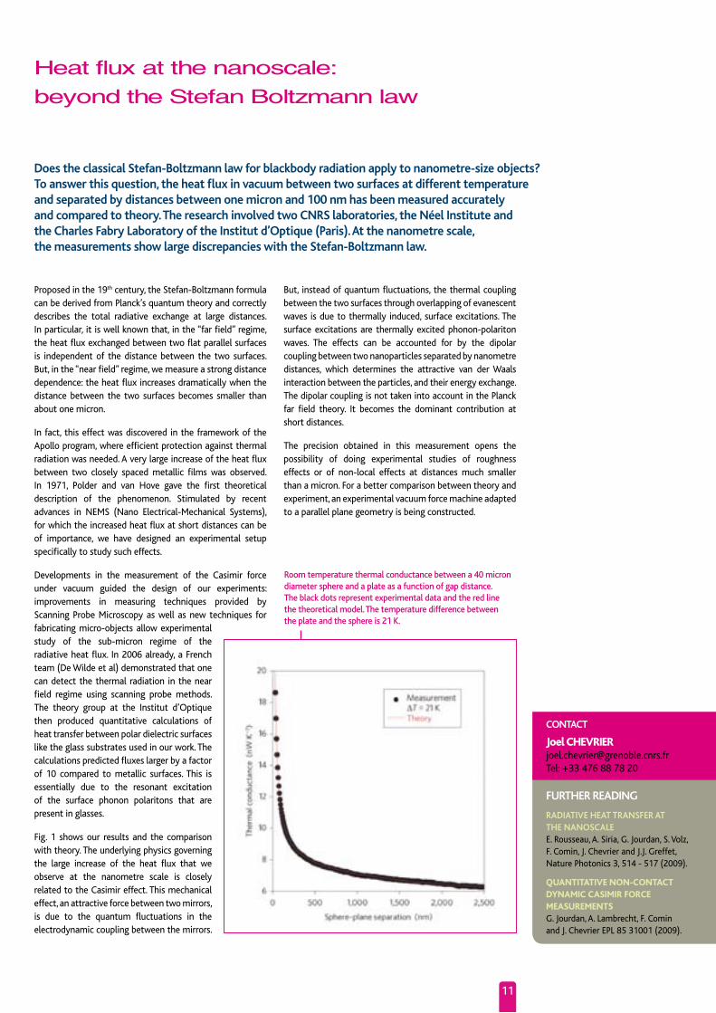
Proposed in the 19th century, the Stefan-Boltzmann formula can be derived from Planck’s quantum theory and correctly describes the total radiative exchange at large distances. in particular, it is well known that, in the “far field” regime, the heat flux exchanged between two flat parallel surfaces is independent of the distance between the two surfaces. But, in the “near field” regime, we measure a strong distance dependence: the heat flux increases dramatically when the distance between the two surfaces becomes smaller than about one micron.
in fact, this effect was discovered in the framework of the Apollo program, where efficient protection against thermal radiation was needed. A very large increase of the heat flux between two closely spaced metallic films was observed. in 1971, Polder and van hove gave the first theoretical description of the phenomenon. Stimulated by recent advances in NEmS (Nano Electrical-mechanical Systems), for which the increased heat flux at short distances can be of importance, we have designed an experimental setup specifically to study such effects.
Developments in the measurement of the casimir force under vacuum guided the design of our experiments: improvements in measuring techniques provided by Scanning Probe microscopy as well as new techniques for fabricating micro-objects allow experimental study of the sub-micron regime of the radiative heat flux. in 2006 already, a French team (De Wilde et al) demonstrated that one can detect the thermal radiation in the near field regime using scanning probe methods. The theory group at the institut d’optique then produced quantitative calculations of heat transfer between polar dielectric surfaces like the glass substrates used in our work. The calculations predicted fluxes larger by a factor of 10 compared to metallic surfaces. This is essentially due to the resonant excitation of the surface phonon polaritons that are present in glasses.
Fig. 1 shows our results and the comparison with theory. The underlying physics governing the large increase of the heat flux that we observe at the nanometre scale is closely related to the casimir effect. This mechanical effect, an attractive force between two mirrors, is due to the quantum fluctuations in the electrodynamic coupling between the mirrors.
But, instead of quantum fluctuations, the thermal coupling between the two surfaces through overlapping of evanescent waves is due to thermally induced, surface excitations. The surface excitations are thermally excited phonon-polariton waves. The effects can be accounted for by the dipolar coupling between two nanoparticles separated by nanometre distances, which determines the attractive van der Waals interaction between the particles, and their energy exchange. The dipolar coupling is not taken into account in the Planck far field theory. it becomes the dominant contribution at short distances.
The precision obtained in this measurement opens the possibility of doing experimental studies of roughness effects or of non-local effects at distances much smaller than a micron. For a better comparison between theory and experiment, an experimental vacuum force machine adapted to a parallel plane geometry is being constructed.
room temperature thermal conductance between a 40 micron diameter sphere and a plate as a function of gap distance. The black dots represent experimental data and the red line the theoretical model. The temperature difference between the plate and the sphere is 21 K.
11
Does the classical Stefan-Boltzmann law for blackbody radiation apply to nanometre-size objects?to answer this question, the heat flux in vacuum between two surfaces at different temperature and separated by distances between one micron and 100 nm has been measured accuratelyand compared to theory. the research involved two cNrS laboratories, the Néel institute and the charles Fabry Laboratory of the institut d’optique (Paris). At the nanometre scale, the measurements show large discrepancies with the Stefan-Boltzmann law.
Heat flux at the nanoscale:
beyond the Stefan Boltzmann law
FurtHer reADiNg
rADiAtive HeAt trANSFer At tHe NANoScALe E. rousseau, A. Siria, G. Jourdan, S. Volz, F. comin, J. chevrier and J.J. Greffet, Nature Photonics 3, 514 - 517 (2009).
QUantItatIve nOn-COntaCt DynamIC CasImIr FOrCe measUrements G. Jourdan, A. Lambrecht, F. comin and J. chevrier EPL 85 31001 (2009).
coNtAct
Joel [email protected]: +33 476 88 78 20

Josephson junction chains are attracting a lot of interest currently due to their possible applications in the fields of metrology and quantum information. For example, under microwave irradiation of frequency f, such chains should exhibit exact current quantization i=2nef, where 2e is the charge of a cooper pair and n is an integer number. therefore, these chains could be used for the definition of a new quantum current standard. in view of the many possible applications, we have measured the ground state of a Josephson junction chain. We have analysed our results in terms of “quantum phase-slips”, the central phenomenon occurring in such superconducting networks.
Néel institute / Highlights 4
A Josephson junction consists of two superconducting electrodes separated by an insulating layer. A phase difference ϕ between the superconducting phases of the two electrodes yields a supercurrent through the junction of the form i(ϕ)=i
c sin(ϕ). The maximum value of this supercurrent,
that is the critical current ic, is fixed by the Josephson energy
EJ. This energy depends on the superconducting gap of
the electrodes and on the normal-state resistance of the junction. The phase difference ϕ over a Josephson junction fluctuates quantum-mechanically due to the presence of the charging energy E
c=q2/2c of the junction capacitance c.
These quantum phase fluctuations induce so-called “quantum phase-slips” where the phase over the junction changes by 2π.
if these phase-slips occur over a junction that is embedded in a chain with many other junctions, new phenomena appear. in this case, a quantum phase-slip on one junction leads to a collective response of all other junctions. This collective behaviour implies the formation of new energy levels ε
n(δ)
that depend on the overall phase difference δ over the chain. The ground state supercurrent through the chain i
chain is
given by the derivative of the ground state energy ε0(δ) with
respect to δ. For a large phase-slip rate υ, that is the number of quantum phase-slips per second, the current-phase relation of a Josephson junction chain is i
chain(δ)=i
cchain sin(δ).
it has the same form as for a single junction but with an effective critical current i
cchain that is given by the quantum
chain dynamics. The critical current icchain is determined by
the number of junctions in the chain and by the quantum phase-slip rate which depends on the ratio of the Josephson energy E
J and the charging energy E
c. We have done the
first quantitative measurement of quantum phase-slips in a Josephson junction chain by measuring its supercurrent as a function of δ.
in our measurements, we determine the ground state of a Josephson junction chain containing six SQUiDs by measuring the critical current of the chain shunted by a read-out junction (figure 1). As each junction of the chain is realized in the form of a SQUiD, we can tune the E
J/E
c ratio in
situ by changing the magnetic flux ΦS through the SQUiDs.
Figure 2 shows the chain’s critical current as a function of flux Φ
S. With increasing flux, we observe the expected
suppression of the critical current due to the increase of quantum fluctuations. From our measurement results we can deduce the quantum phase-slip rate υ. it varies over a range from 1 to 3 Ghz (see inset of figure 2).
our results open the way for the use of quantum phase-slips in Josephson junction networks for the implementation of a new current standard or the fabrication of topologically protected qubits.
Figure 1: E-beam image of the sample, a) six SQuID chain shunted by the read-out junction, b) one SQuID, c) one SQuID junction, d) the read-out junction.
Figure 2: measured critical current (black points) as a function of flux Φ
S/Φ
0 through the SQuID.
The red curve is the theoretical fit. Inset: Quantum phase-slip rate υ as a function of flux.
coNtActS
wiebke [email protected]: +33 (0)476 88 78 20
Olivier [email protected]: +33 476 88 90 66
Effect of quantum phase-slips in a Josephson junction chain
12
FurtHer reADiNg
meASuremeNt oF tHe eFFect oF quANtum PHASe-SLiPS iN A JoSePHSoN JuNctioN cHAiN i. m. Pop, i. Protopopov, F. Lecocq, Z. Peng, B. Pannetier, o. Buisson, W. Guichard, Nature Physics 6, 1697 (2010).
meASuremeNt oF tHe curreNt-PHASe reLAtioN iN JoSePHSoN JuNctioN rHomBi cHAiNSi. m. Pop, K. hasselbach, o. Buisson, W. Guichard, B. Pannetier, and i. Protopopov, Phys. rev. B 78, 104504 (2008).

FurtHer reADiNg
eviDeNce For quANtum- coNFiNeD StArK eFFect iN gAN/ALN quANtum DotS iN NANoWireSJ. renard, r. Songmuang, G. Tourbot, c. Bougerol, B. Daudin, B. Gayral, Phys. rev. B 80, 121305 (2009).
quANtum trANSPort iN gAN/ALN DouBLe-BArrier HeteroStructure NANoWireSr. Songmuang, G. Katsaros, E. monroy, P. Spathis, c. Bougerol, m. mongillo and S. De Franceschi, ArXiv:1005.3637 (2010).
Nanowires are considered to be very promising as building blocks for nano-scale devices and as a new route to access the physics of low dimensional systems. For iii-N compounds (nitrides of group iii elements), nanowire heterostructures provide a new way to create quantum dots, with greater flexibility as compared to the classic Stranski-Krastanow growth mode because the dot height and the material composition can be better controlled. Furthermore, while the strain induced by the large lattice mismatch usually leads to high dislocation density in planar iii-N nanostructures, it can relax elastically (radially) in thin nanowires, allowing dislocation free growth.
currently, nearly all the studies on iii-N quantum dots have been oriented towards their photonic aspects. in the present work we focus on probing such structures via electrical measurements. We have fabricated single GaN quantum dots in the form of iii-N nanowire heterostructures and we have measured electronic transport through these dots. our results indicate that GaN quantum dots formed in a nanowire are promising objects for accessing the low dimensional electronic properties of iii-N materials.
We grow wurtzite GaN nanowires on Si (111) substrates by plasma-assisted molecular Beam Epitaxy without using any catalyst (Fig. 1(a)). The GaN quantum dots were fabricated by introducing two AlN tunnel barriers into the GaN nanowires (see the high resolution TEm image in Fig. 1(b)). After growth, the nanowires were mechanically dispersed so as to lie horizontally on a Sio
2 layer on top of a high conductivity
Si substrate. For electronic transport measurements, nanowires were electrically contacted by metal electrodes (source and drain) formed by electron beam lithography (Fig. 2(a)). The heavily doped silicon substrate was used as the gate electrode.
Electronic transport through GaN
quantum dots in nanowires
The diagram of the differential conductance di/dVSD
versus source-drain voltage (V
SD) and gate voltage (V
G) at 4.2 K
shows a series of diamond shaped regions where transport is entirely suppressed (blue regions in Fig. 2(b)). These “coulomb diamonds” are clearly separated from each other and have all their edges fully defined. This is characteristic of coulomb-blockaded transport of single electrons through a single island. here the island is the quantum dot grown in the GaN wire. Within each coulomb diamond the quantum dot contains a fixed number of electrons. The periodicity along the V
G axis, which is related to the length of the island
through which transport takes place, is consistent with the length, as given by electron microscopy, of the GaN dot in between its two AlN tunnel barriers.
Studies of this type have already been done on several types of nano-scale islands of Si, Group iii arsenides and metals. our results demonstrate for the first time, single electron transport through single GaN/AlN quantum dots in nanowires. This work is not only valuable for the application of iii-N nanowires, but also for a deeper understanding of quantum transport in nitride materials, which is mostly unexplored.
coNtActS
rudeesun sOnGmUanG [email protected]: +33 438 78 54 16
Giorgos KatsarOs [email protected]
Figure 1: (a): Transmission Electron Microscopy (TEM) image of a gaN nanowire ensemble grown on a Si (111) substrate.
(b): High resolution TEM image of a gaN nanowire containing a double barrier heterostructure, i.e. a pair of 2 nm thick alN tunnel barriers (bright contrast) separated by a 6 nm height gaN quantum dot layer (dark constrast).
Figure 2: (a): Schematic illustration of a gaN nanowire device with double tunnel barriers contacted by metal leads. The nanowire is deposited on an oxidized Si substrate.
(b): color scale plot of the differential conductance dI/dVSD
versus source-drain voltage V
SD and gate-voltage V
g for a gaN quantum dot formed in a nanowire.
The measurement is taken at 4.2 K. Blue (red) color corresponds to low (high) conductance.
13

Néel institute / Highlights 4
60 years ago and half a century after helium gas was first liquefied by Kamerlingh onnes in Leiden (1908), the cNrS laboratory in grenoble became a centre for helium liquefaction. today the liquefaction centre at the Néel institute is the largest in France. We recall here the history of this development from its origin to the present day.
Néel institute / Highlights 4
Louis Néel and Louis Weil arrived in Grenoble during World War ii. At the end of the war, there was an obvious need for cryogenic fluids to allow them to extend their research on magnetism down to very low temperatures. in 1947, Weil engaged Albert Lacaze to build an apparatus to produce liquid hydrogen (boiling point 20 K); this was Lacaze’s doctoral research project. The liquefier constructed by Lacaze was based on the Joule Thomson expansion of hydrogen at 150 bars and pre-cooled by a pumped liquid nitrogen bath (62 K).
The Weil-Lacaze liquefier was installed in the basement of the institut Fourier building in central Grenoble (with the basement windows kept open for ventilating any hydrogen leaks...). By 1950, it could produce 15 litres of liquid hydrogen in an hour. in that year 1950, Weil and Lacaze were able to liquify helium (4 K), using the same principle, with liquid hydrogen replacing liquid nitrogen as initial coolant. Because handling liquid hydrogen was a difficult and a dangerous matter (especially while decanting it from one liquefier to another), a hybrid apparatus combining the two liquefaction stages -hydrogen and helium- soon replaced the initial installation.
By 1956, their prototype mixed liquefier was producing 100 litres of liquid helium and 400 litres of liquid hydrogen per year. it ensured hydrogen and helium production for the Grenoble laboratories until 1962. This class of liquefier, in use until the early seventies, was commercialized by the Très Basses Températures (Very Low Temperatures) company, founded by Louis Weil in 1956. The TBT company also manufactured cryogenics components such as transfer tubes and storage vessels.
in 1958, the Air Liquide company bought TBT. The creation, several years later, of Air Liquide’s centre for cryogenics Studies near Grenoble at Sassenage is probably one of the consequences of this collaboration. The Sassenage centre later became the Division of Advanced Technologies of Air Liquide.
60 years of liquid Helium production
at the CNRS in Grenoble
14
evolution of annual production of liquid helium by the cNrS in grenoble. today the liquefaction centre at the Néel institute is the largest in France. it produces more than 500000 litres of liquid helium a year, of which 400000 litres are dispatched to cNrS and university laboratories in the grenoble area. in partnership with the liquefaction service of the institute of Nanosciences and cryogenics (iNAc) at the ceA-grenoble, it supplies liquid helium to grenoble’s two large european research facilities, the european Synchrotron radiation Facility (eSrF) and the Laue Langevin institute (iLL).
Louis WEIL
albert LacazE
TBT Helium Liquefier (copyright: atelier robert Doisneau).
coNtActS
philippe [email protected]: +33 476 88 90 69
Christian [email protected]: +33 476 88 12 77
in 1971, the cNrS in Grenoble acquired a Philips liquefier (10 litres helium/hour) and constructed the present liquefier building. Turbine liquefiers arrived shortly afterwards, increasing the liquefaction rates dramatically. in 1976, a “hélial” helical turbine liquefier producing 40 litres/hour was purchased from Air Liquide. As the needs of the cNrS laboratories continued to increase, two more liquefiers were added: the first in 1986 (100 litres/hour) and the second (replacing the first hélial) in 1996.
FurtHer reADiNg
eviDeNce For A DiSorDer- DriveN PHASe trANSitioN iN tHe coNDeNSAtioN oF 4He iN AerogeLS Bonnet, T. Lambert, B. cross, L. Guyon, F. Despetis, L. Puech et P. E. Wolf, Europhysics Letters 82 56003 (2008). EPL Editor’s choice 2008.
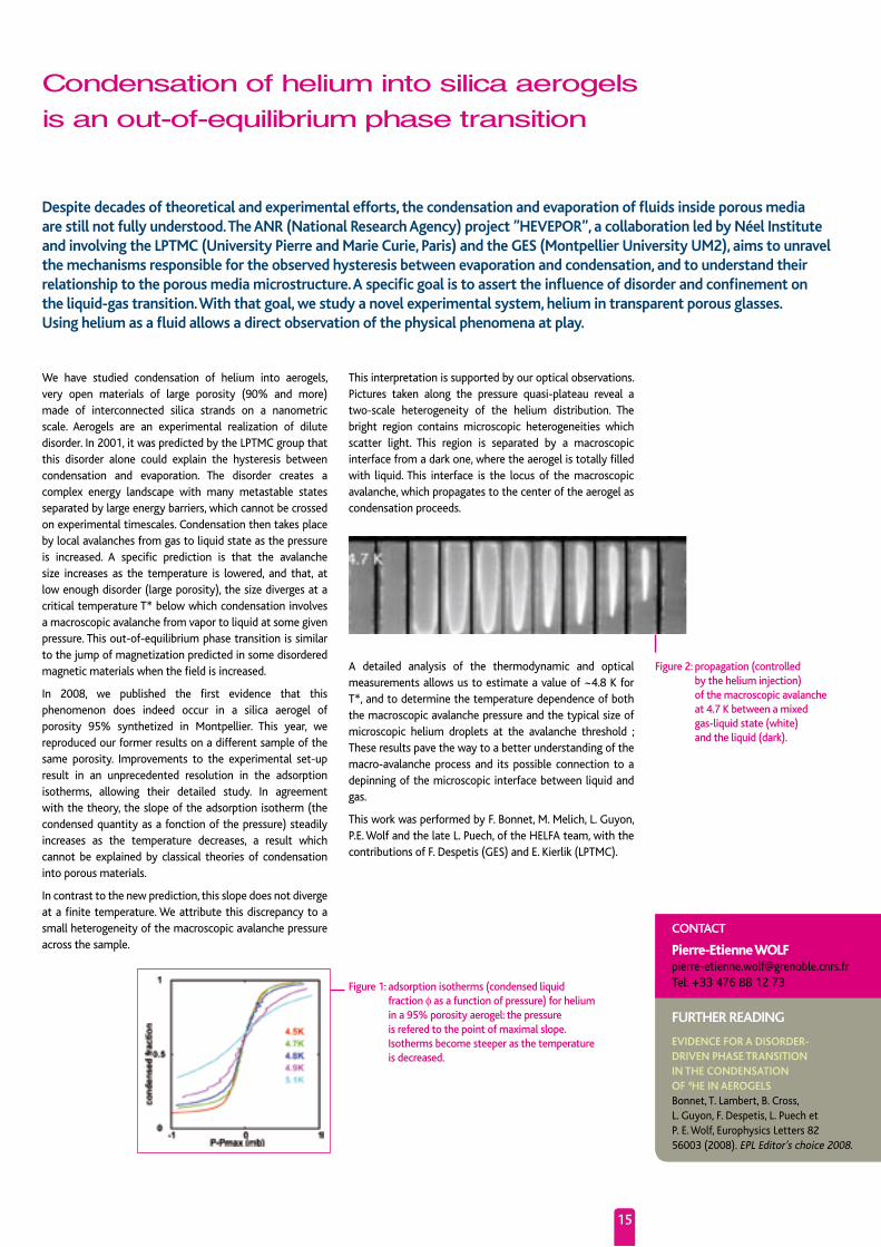
We have studied condensation of helium into aerogels, very open materials of large porosity (90% and more) made of interconnected silica strands on a nanometric scale. Aerogels are an experimental realization of dilute disorder. in 2001, it was predicted by the LPTmc group that this disorder alone could explain the hysteresis between condensation and evaporation. The disorder creates a complex energy landscape with many metastable states separated by large energy barriers, which cannot be crossed on experimental timescales. condensation then takes place by local avalanches from gas to liquid state as the pressure is increased. A specific prediction is that the avalanche size increases as the temperature is lowered, and that, at low enough disorder (large porosity), the size diverges at a critical temperature T* below which condensation involves a macroscopic avalanche from vapor to liquid at some given pressure. This out-of-equilibrium phase transition is similar to the jump of magnetization predicted in some disordered magnetic materials when the field is increased.
in 2008, we published the first evidence that this phenomenon does indeed occur in a silica aerogel of porosity 95% synthetized in montpellier. This year, we reproduced our former results on a different sample of the same porosity. improvements to the experimental set-up result in an unprecedented resolution in the adsorption isotherms, allowing their detailed study. in agreement with the theory, the slope of the adsorption isotherm (the condensed quantity as a fonction of the pressure) steadily increases as the temperature decreases, a result which cannot be explained by classical theories of condensation into porous materials.
in contrast to the new prediction, this slope does not diverge at a finite temperature. We attribute this discrepancy to a small heterogeneity of the macroscopic avalanche pressure across the sample.
This interpretation is supported by our optical observations. Pictures taken along the pressure quasi-plateau reveal a two-scale heterogeneity of the helium distribution. The bright region contains microscopic heterogeneities which scatter light. This region is separated by a macroscopic interface from a dark one, where the aerogel is totally filled with liquid. This interface is the locus of the macroscopic avalanche, which propagates to the center of the aerogel as condensation proceeds.
A detailed analysis of the thermodynamic and optical measurements allows us to estimate a value of ~4.8 K for T*, and to determine the temperature dependence of both the macroscopic avalanche pressure and the typical size of microscopic helium droplets at the avalanche threshold ; These results pave the way to a better understanding of the macro-avalanche process and its possible connection to a depinning of the microscopic interface between liquid and gas.
This work was performed by F. Bonnet, m. melich, L. Guyon, P.E. Wolf and the late L. Puech, of the hELFA team, with the contributions of F. Despetis (GES) and E. Kierlik (LPTmc).
Figure 2: propagation (controlled by the helium injection) of the macroscopic avalanche at 4.7 K between a mixed gas-liquid state (white) and the liquid (dark).
Despite decades of theoretical and experimental efforts, the condensation and evaporation of fluids inside porous media are still not fully understood. the ANr (National research Agency) project ”HevePor”, a collaboration led by Néel institute and involving the LPtmc (university Pierre and marie curie, Paris) and the geS (montpellier university um2), aims to unravel the mechanisms responsible for the observed hysteresis between evaporation and condensation, and to understand their relationship to the porous media microstructure. A specific goal is to assert the influence of disorder and confinement on the liquid-gas transition. With that goal, we study a novel experimental system, helium in transparent porous glasses. using helium as a fluid allows a direct observation of the physical phenomena at play.
coNtAct
pierre-etienne wOLF [email protected]: +33 476 88 12 73
Condensation of helium into silica aerogels
is an out-of-equilibrium phase transition
15
Figure 1: adsorption isotherms (condensed liquid fraction f as a function of pressure) for helium in a 95% porosity aerogel: the pressure is refered to the point of maximal slope. Isotherms become steeper as the temperature is decreased.

ESoNN 2009.
the 6th eSoNN (european School on Nanosciences and Nanotechnologies) took place from August 22nd to September 12th 2009 in grenoble. eSoNN is a summer school organised each year by the université Joseph Fourier and grenoble iNP, with the essential participation of the cNrS and the ceA. it is designed for doctoral students and young researchers interested in nanosiences. eSoNN’s specificity is to associate lectures given by top european specialists with practical sessions at the “centre inter-universitaire de micro-electronique ” (cime) and in grenoble research institutes.
European School on Nanosciences
and Nanotechnologies
Two parallel sessions are offered, one on quantum nano-electronics (mesoscopic transport, molecular electronics, spintronics, single-electron components, ultimate moSFET’s), the second on nanomaterials for life sciences (surface physical-chemistry, microsystems for biophysics, rheology of biological structures, microfluidics, nano-object synthesis). Joint lectures on nanotechnology (nanofabrication, local probe microscopy, bottom-up techniques) are followed by all attendees.
Albert Fert, winner of the 2007 Nobel Prize in Physics for his pioneering works on spintronics, gave the opening lecture at the 6th ESoNN. That school was attended by 56 students selected from over 110 applications. A total of 25 nationalities were represented: Austria (1), Brazil (3), canada (1), china (2), croatia (1), Denmark (4), Finland (3), France (4), Germany (1), hungary (1), india (4), iran (1), italy (5), Jamaica (1), Lebanon (1), Pakistan (1), Peru (1), Poland (2), Portugal (2), russia (3), South Africa (2), Spain (5), Thailand(1), Turkey (3) and the United States (3). The participation of indian and Brazilian students was made possible by regional ArcUS programs. The US participants were financed by the houston French consulate.
FurtHer reADiNg
eSoNN rePortS 2004-2009
coNtAct
Hervé [email protected]: +33 476 88 11 51web site: www.esonn.fre-mail: [email protected]
Among the 50 laboratory practicals offered in 2009, 10 were organized by Néel institute on the following topics: optical and electrical characterization of wide bandgap semiconductor single nanowires, E-beam lithography and FiB techniques for micro-nanofabrication, magnetoresistive effects in magnetic heterostructures, Electro-migration technique to realize a single molecule transistor, coulomb blockade in carbon Nanotube Transistors, carbon Nanotube synthesis and optical characterization by raman spectroscopy, X-ray scattering from films and superlattices, Seeing real-time electron tunneling processes, confocal spectroscopy on small objects, Force measurements with a micro-mechanical oscillator based on a tuning fork. These one day practicals have been prepared by doctoral students, engineers, and researchers from Néel institute.
ESoNN is financed by the following: Université Joseph Fourier, Grenoble iNP, Grenoble Nanoscience Fondation, cNrS, Nano-innov program, French National Education ministry (“European Summer campus”), rhône-Alpes regional council, Grenoble city and mETro councils.
The 7th school, now in preparation, has a similar program of lectures and practicals. it will also include a program on technology transfer for high tech industries (prepared in collaboration with the Grenoble School of management) and societal issues for nanosciences and nanotechnologies. Ethical aspects and risk assessment for nano-materials will be covered during evening seminars.
albert FErT & Hervé courToIS.
16

17
overview of the lecture Hall
computer tutorials (here micromagnetism, 4h).
The core of the organization of ESm relies on research scientists from Néel institute and Spintec. it is supported by many institutions and most notably UJF and cNrS, and is guided by a European scientific committee. The upcoming events will be more closely associated with the bi-annual, largest European conference on magnetism JEmS (Joint European magnetic Symposia), which itself was initiated and first held in Grenoble in 2001. This new association should further increase the attractiveness of ESm, and through it the key role played by Grenoble laboratories and universities in modern magnetism.
there have been long-standing research and teaching collaborations between romania and France, most notably with grenoble. Néel institute plays an active role through its hosting of colleagues and students from several romanian universities, in particular cluj-Napoca (Babes-Bolyai). the latter’s Faculty of Physics has many common interests with Néel institute (condensed matter Physics, magnetism, materials...), which has led to a constant influx of master level romanian students to grenoble. many students have continued to PhD level at the université Joseph Fourier or grenoble iNP, in many cases the thesis work being co-supervised.
research schools intended for graduate students have been organized jointly in romania since 1997, with topics mostly related to magnetism.
The first schools were conducted in French and gathered French and romanian students. Since 2003 the schools have been conducted in English and progressively became more international, concerning both the choice of lecturers and attendees. consequently, this series of schools has been renamed the European School on magnetism (ESm). in 2009 ESm was held in Timisoara with the topic “models in magnetism: from basic aspects to practical uses”. 120 attendees were registered on a first-come first-served basis. These were mostly PhDs and post-docs counting 31 nationalities and coming from 23 countries, mainly European.
Through a constant evolution the School has created a unique pedagogical environment, informal and interactive, where students truly get the most out of teaching: ten full days duration, both lectures and tutorials, question sessions, open-access library dedicated to magnetism etc.
coNtActS
Claudine [email protected]: +33 476 88 10 98
Olivier [email protected]: +33 476 88 79 20
Olivier [email protected]: +33 476 88 11 46
From a French-Romanian collaboration
to the European School on Magnetism
FurtHer reADiNg
WeB Site: HttP://eSm.NeeL.cNrS.Fr

Néel institute / Highlights 4
18
Experimental information about the elements dissolved in a fluid phase at high temperatures and pressures are needed: their speciation (i.e. their chemical and structural form) and their thermodynamics data (i.e. the stability of the different species present as a function of temperature, pressure, salinity). To obtain such information, we have developed a new methodology based on the use of X-ray Absorption Spectroscopy.
We use a dedicated, high pressure autoclave designed and developed at the Néel institute by r. Argoud. The autoclave is equipped with beryllium windows for X-ray absorption and fluorescence spectroscopy measurements. it is installed on FAmE (the French Absorption spectroscopy beamline for material and Environmental sciences) at the European Synchrotron radiation Facility in Grenoble. This experimental development allows us to cover a large domain of the phase diagram (pressures 1-2000 bars, temperatures 30-600 °c, densities down to 0.1 g.cm-3), corresponding to conditions existing in the real Earth. Since iron is both a typical and an ubiquitous element in the Earth’s crust and mantle, we have investigated using this instrument the fate of aqueous iron in hydrothermal (i.e. high temperature and pressure) conditions.
First we explored the speciation from ambient up to supercritical conditions (500°c, 500 bar), as a function of temperature and chlorinity of the solutions (i.e. the quantity of dissolved chlorine ions).
in the present economic and ecological context, two primordial fields of research in earth Sciences are (i) developing methods for sequestration of co
2 in mineral form as stable
carbonate rocks and (ii) understanding the formation of metal-ore deposits in view of the prospection of new, mineable resources. A common aspect of these two research fields is understanding the complex processes of dissolution/precipitation of rocks in aqueous fluids.
Iron in hydrothermal fluids: fundamental geochemical
processes studied by synchrotron radiation
FurtHer reADiNg
AN X-rAy ABSorPtioN StuDy oF tHe DiSSoLutioN oF SiDerite At 300 BAr BetWeeN 50°c AND 100°c, cHem. geoL. 259, 8 (2009)D. Testemale, F. Dufaud, i. martinez, P. Bénézeth, J.L. hazemann, J. Schott, and F. Guyot
iN-Situ X-rAy ABSorPtioN StuDy oF iroN(ii) SPeciAtioN iN BriNeS uP to SuPercriticAL coNDitioNS, cHem. geoL. 264, 295 (2009)D. Testemale, J. Brugger, W. Liu, B. Etschmann, and J.L. hazemann
coNtActS
Jean-Louis [email protected]: +33 476 88 74 07
Denis [email protected]: +33 476 88 10 45
yves [email protected]: +33 476 88 74 12
The near edge X-ray Absorption spectrum is very sensitive to the local environment of solvated iron. recent theoretical progress in ab initio calculations of the X-ray Absorption Near-Edge Structure (XANES) using Finite Difference method (FDmNES) calculations allowed us to interpret the spectral signature of the iron complexes and to observe their transition from octahedral hydrated species Fe(h
2o)
62+
to tetrahedral chlorinated species Fecl4
2- (see figure). This investigation was performed in collaboration with Adelaide University & cSiro (Australia).
Secondly, we studied the dissolution/precipitation reaction of siderite (Feco
3) in hydrothermal conditions, a model reaction
for an essential step in proposed methods to sequester co2 as
metal carbonates. in nature, this corresponds to the final step of carbonatation (transformation to carbonate) once Fe2+ is released in solution by earlier dissolution of other iron-bearing rocks, such as the silicates widely present in the Earth’s crust and mantle. measuring in situ the X-ray transmission of the carbonate solution, we determine iron concentration and we derive kinetics parameters and thermodynamics data such as dissolution rate constants, activation energies, dependence on ph and chlorinity. Simultaneously, the iron speciation was also determined by X-ray fluorescence spectroscopy.
This work, done in collaboration with the institut de minéralogie et de Physique des milieux condensés (imPmc, Paris) on a model dissolution reaction, provides an overall set of speciation, thermodynamics & kinetics data. Data of this kind is essential for geochemical modeling. Through our current national and international collaborations, we are extending these methods to other aqueous geochemical systems (cu, co, Ga, Au, Ag, etc.).
observed changes of iron speciation in saline aqueous solution. at low chlorine concentration and/or low temperature, Fe2+ ions are hydrated by 6 water molecules in an octahedral symmetry; in high salinity and/or high temperature (i.e. hydrothermal) conditions up to 500°c, Fe2+ ions are coordinated by 4 chloride ions cl- in a tetrahedral symmetry.
high T, high salinityLow T, low salinity

Figure 1: (a,b) Schematic diagrams of the TMP process and magneto-optic
imaging with a uniaxial Magneto-optic-Indicator-Film (u-MoIF),
(c) Magneto-optic image of aMoIF placed on top of a uniaxially patterned out-of-plane textured NdFeB film irradiated through a mask with features of size 50 x 50 µm,
(d) MFM image of a similar film patterned with a mask containing features of size 7 × 7 µm2.
19
micro flux sources produce magnetic fields which are spatially modulated at the micron scale. they have many potential applications in the field of magnetic memS (micro-electro-mechanical-Systems), as well as for biasing, diamagnetic levitation, the manipulation and trapping of particles and atoms, etc. the magnetic force on a magnetic particle submitted to the field of such a flux source depends on the field and on the field gradient created by the source. Since the field gradient is inversely proportional to the size of the field source, the force per unit volume increases as its size is reduced.
The use of permanent magnets to produce the flux offers a number of specific advantages. it favours autonomy and stability. By comparison, micro-patterned soft magnetic materials require the application of an external magnetic field while micro-coils operating in Dc mode produce much smaller fields and field gradients. The challenge in fabricating micro-permanent magnet based sources is first of all to produce hard magnetic films of the appropriate thickness (1-100 µm). We have demonstrated that triode sputtering is suitable for the preparation of high performance hard magnetic films (NdFeB, Smco) in thick film form. The second challenge is to laterally pattern the films on the scale of 1-100 µm. in a first approach we showed that standard micro-fabrication techniques (lithography, etching, planarization) can be applied to these highly reactive films (collaboration LETi). here we will present an alternative and very promising patterning technique, namely Thermo-magnetic Patterning (TmP).
When we heat a hard magnetic film we reduce its coercivity, i.e. the value of external magnetic field required to reverse its magnetisation. TmP (fig. 1(a)) exploits this fact to locally modify the direction of magnetisation, by localised heating through a mask in the presence of a magnetic field which is lower than the film’s room temperature value of coercivity. An excimer laser operated in nanosecond pulsed mode at an ultralviolet wavelength is used so as to minimise reflection at the film’s surface and lateral heat diffusion through the hard magnetic film. Qualitative magnetic imaging using magneto-optic-indicator-Films (moiF) (fig. 1b) and magnetic Force microscopy (mFm) reveals the magnetic patterns with
Permanent magnet micro flux sources
FurtHer reADiNg
N. m. DemPSey et AL., APPL. PHyS. Lett. 90, 092509 (2007).
F. DumAS-BoucHiAt et AL., APPL. PHyS. Lett. 96, 102511 (2010).
coNtAct
Frédéric [email protected] Tel.: +33 476 88 74 33
lateral dimensions of roughly 50 µm and 7µm, respectively, which have been produced by TmP of 5µm thick out-of-plane textured NdFeB films (fig. 1c,d).
The stray field patterns produced by these hard magnet micro-flux sources have been quantitatively characterised using a Scanning hall Probe microscope. comparing these measurements with calculations we have estimated the depth of film over which magnetisation had been reversed by TmP to be of the order of 1.3 µm.
These hard magnet micro-flux sources constitute traps for superparamagnetic (SPm) particles and biological species incorporating superparamagnetic particles (collaboration Ampere Lab. Lyon). Preliminary experiments show that the magnetic field gradients produced at the interface between reversed and non-reversed regions of the hard magnetic films are strong enough (>106 T/m) to attract and trap 100 nm sized SPm particles flowing in a micro-fluidic channel above the film (fig. 2a). What is more, bacteria of 1µm in size (escherichia coli) internalised with the SPm particles by electroporation can also be trapped at these regions of high field gradient (fig. 2b). These preliminary results show the great potential for the use of permanent magnet micro flux sources for lab-on-chip applications in biology and medicine.
Figure 2: (a) (collaboration ampere Lab,
Ecole centrale Lyon). optical image showing the trapping of superparamagnetic particles within a PDMS micro-fluidic channel (width: 500µm, height: 100µm) above a TMP NdFeB film,
(b) Fluorescent image showing the trapping of bacteria internalised with superparamagnetic particles on a TMP NdFeB film.
TmP can be used to produce complex magnetic field configurations such as linear halbach arrays, for which flux is maximised on one side and minimised on the other side of the array. A linear halbach array prepared by TmP of an isotropic NdFeB film is shown in figure 3. This demonstrates the potential for TmP to produce complex patterns at the micro-scale and should allow us to optimise the use of micro-flux sources in identified applications and eventually open the door to new applications.
Figure 3: magneto-optic image of a MoIF placed on top of a thermo-magnetically patterned linear Halbach array and schematic diagram showing the direction of the applied magnetic field during TMP.

Néel institute / Highlights 4
13
recently, we have demonstrated, first, that the hole mobility could be optimized and what kind of defects may degrade it and, second, that unprecedented breakdown voltages, in excess of 10 kV, can be obtained in Schottky diodes if a specific surface oxidizing treatment is applied. This treatment ensures both electrical passivation of the surface and chemical passivation of the metallic interface. These findings open the route to high voltage and high power devices for power electronics and electrical energy management.
These achievements are the results of new diamond growth conditions developed at the Néel institute for better control of dopant incorporation, as well as a new surface treatment method based on ozone produced by Vacuum UV, developed in collaboration with the NimS Laboratory (Tsukuba, Japan).
Device simulations and studies of high voltage bias conditions in air were performed at the AmPErE Laboratory (iNSA Lyon). Finally, very high voltage was applied to a diamond device at iSL (institut Franco-Allemand de recherches de Saint-Louis), demonstrating a 10kV break-down voltage for the diamond rectifier. For the first time, the breakdown field of 10 mV/cm predicted a long time ago might really determine the maximum voltage of these diodes, because of their ideal surface and interface passivations. other device architectures, using both heavily and lightly doped diamond epilayers, have also been investigated. They demonstrated current densities in the forward regime as high as 50 A/cm2 under 4 volts at 300 K.
These new results show that diamond is well able to fulfil its promise, provided that appropriate growth methods and treatments are implemented. Such advances pave the way to high voltage and high power electronic devices, with superior performance in comparison to usual silicon or to innovative silicon carbide devices.
Diamond is a wide bandgap semiconductor (eg = 5.5 ev) with astounding electronic,
thermal, optical, mechanical and chemical properties, which have been recognized for several decades. Steady progress has been achieved in understanding and mastering crystalline quality and defects, dopant concentrations, carrier mobility and saturation velocity, breakdown voltage and surface terminations, which control the electrical properties of homoepitaxial layers used in electronic devices.
Breaking records in diamond devices
current density vs d.c. voltage applied to a diamond Schottky diode at 300 K in vacuum, showing the 10kV reverse breakdown voltage. a picture of the diamond crystal is displayed in the inset, with the four ohmic contacts in the corners and 49 diodes in the center.
FurtHer reADiNg
HigH HoLe moBiLity iN BoroN-DoPeD DiAmoND For PoWer Device APPLicAtioNSP.-N. Volpe, J. Pernot, P. muret, F. omnès, Appl. Phys. Letters 94, 092102 (2009)
coNtAct
Julien [email protected]: +33 456 38 70 83
20
Breaking records in diamond devices
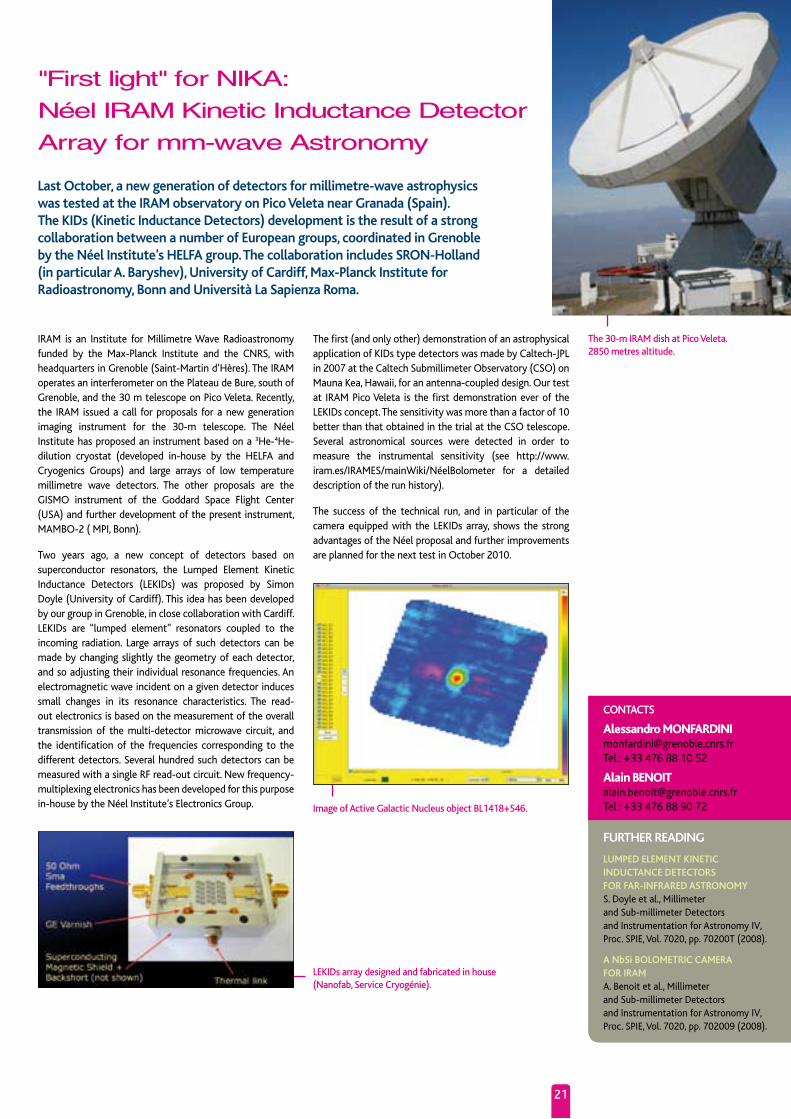
Last october, a new generation of detectors for millimetre-wave astrophysics was tested at the irAm observatory on Pico veleta near granada (Spain). the KiDs (Kinetic inductance Detectors) development is the result of a strong collaboration between a number of european groups, coordinated in grenoble by the Néel institute’s HeLFA group. the collaboration includes SroN-Holland (in particular A. Baryshev), university of cardiff, max-Planck institute for radioastronomy, Bonn and università La Sapienza roma.
irAm is an institute for millimetre Wave radioastronomy funded by the max-Planck institute and the cNrS, with headquarters in Grenoble (Saint-martin d’hères). The irAm operates an interferometer on the Plateau de Bure, south of Grenoble, and the 30 m telescope on Pico Veleta. recently, the irAm issued a call for proposals for a new generation imaging instrument for the 30-m telescope. The Néel institute has proposed an instrument based on a 3he-4he-dilution cryostat (developed in-house by the hELFA and cryogenics Groups) and large arrays of low temperature millimetre wave detectors. The other proposals are the GiSmo instrument of the Goddard Space Flight center (USA) and further development of the present instrument, mAmBo-2 ( mPi, Bonn).
Two years ago, a new concept of detectors based on superconductor resonators, the Lumped Element Kinetic inductance Detectors (LEKiDs) was proposed by Simon Doyle (University of cardiff). This idea has been developed by our group in Grenoble, in close collaboration with cardiff. LEKiDs are “lumped element” resonators coupled to the incoming radiation. Large arrays of such detectors can be made by changing slightly the geometry of each detector, and so adjusting their individual resonance frequencies. An electromagnetic wave incident on a given detector induces small changes in its resonance characteristics. The read-out electronics is based on the measurement of the overall transmission of the multi-detector microwave circuit, and the identification of the frequencies corresponding to the different detectors. Several hundred such detectors can be measured with a single rF read-out circuit. New frequency-multiplexing electronics has been developed for this purpose in-house by the Néel institute’s Electronics Group.
"First light" for NIKA:
Néel IRAM Kinetic Inductance Detector
Array for mm-wave Astronomy
FurtHer reADiNg
LumPeD eLemeNt KiNetic iNDuctANce DetectorS For FAr-iNFrAreD AStroNomyS. Doyle et al., millimeter and Sub-millimeter Detectors and instrumentation for Astronomy iV, Proc. SPiE, Vol. 7020, pp. 70200T (2008).
A NbSi BoLometric cAmerA For irAmA. Benoit et al., millimeter and Sub-millimeter Detectors and instrumentation for Astronomy iV, Proc. SPiE, Vol. 7020, pp. 702009 (2008).
coNtActS
alessandro [email protected].: +33 476 88 10 52
alain [email protected] Tel.: +33 476 88 90 72Image of active galactic Nucleus object BL1418+546.
LEKIDs array designed and fabricated in house (Nanofab, Service cryogénie).
The first (and only other) demonstration of an astrophysical application of KiDs type detectors was made by caltech-JPL in 2007 at the caltech Submillimeter observatory (cSo) on mauna Kea, hawaii, for an antenna-coupled design. our test at irAm Pico Veleta is the first demonstration ever of the LEKiDs concept. The sensitivity was more than a factor of 10 better than that obtained in the trial at the cSo telescope. Several astronomical sources were detected in order to measure the instrumental sensitivity (see http://www.iram.es/irAmES/mainWiki/NéelBolometer for a detailed description of the run history).
The success of the technical run, and in particular of the camera equipped with the LEKiDs array, shows the strong advantages of the Néel proposal and further improvements are planned for the next test in october 2010.
21
The 30-m IraM dish at Pico Veleta.2850 metres altitude.
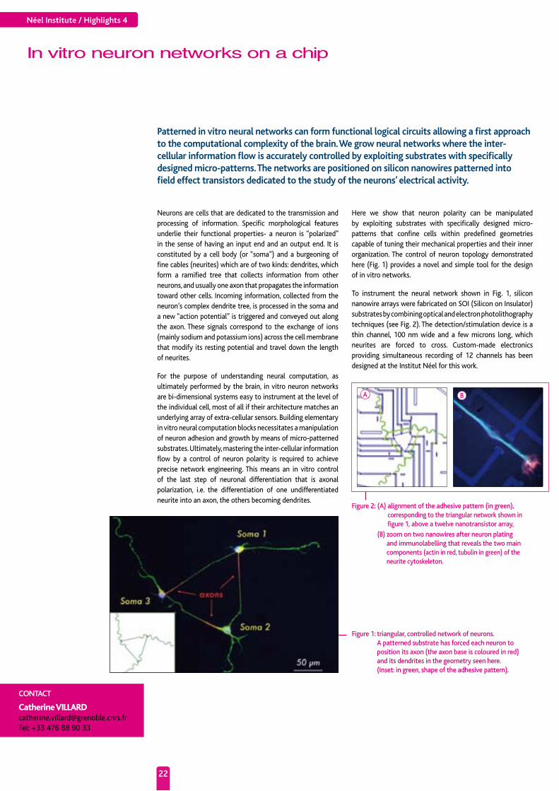
Figure 1: triangular, controlled network of neurons. a patterned substrate has forced each neuron to position its axon (the axon base is coloured in red) and its dendrites in the geometry seen here. (Inset: in green, shape of the adhesive pattern).
Neurons are cells that are dedicated to the transmission and processing of information. Specific morphological features underlie their functional properties- a neuron is “polarized” in the sense of having an input end and an output end. it is constituted by a cell body (or “soma”) and a burgeoning of fine cables (neurites) which are of two kinds: dendrites, which form a ramified tree that collects information from other neurons, and usually one axon that propagates the information toward other cells. incoming information, collected from the neuron’s complex dendrite tree, is processed in the soma and a new “action potential” is triggered and conveyed out along the axon. These signals correspond to the exchange of ions (mainly sodium and potassium ions) across the cell membrane that modify its resting potential and travel down the length of neurites.
For the purpose of understanding neural computation, as ultimately performed by the brain, in vitro neuron networks are bi-dimensional systems easy to instrument at the level of the individual cell, most of all if their architecture matches an underlying array of extra-cellular sensors. Building elementary in vitro neural computation blocks necessitates a manipulation of neuron adhesion and growth by means of micro-patterned substrates. Ultimately, mastering the inter-cellular information flow by a control of neuron polarity is required to achieve precise network engineering. This means an in vitro control of the last step of neuronal differentiation that is axonal polarization, i.e. the differentiation of one undifferentiated neurite into an axon, the others becoming dendrites.
Patterned in vitro neural networks can form functional logical circuits allowing a first approach to the computational complexity of the brain. We grow neural networks where the inter-cellular information flow is accurately controlled by exploiting substrates with specifically designed micro-patterns. the networks are positioned on silicon nanowires patterned into field effect transistors dedicated to the study of the neurons’ electrical activity.
In vitro neuron networks on a chip
coNtAct
Catherine [email protected]: +33 476 88 90 33
Néel institute / Highlights 4
Figure 2: (a) alignment of the adhesive pattern (in green), corresponding to the triangular network shown in figure 1, above a twelve nanotransistor array,
(B) zoom on two nanowires after neuron plating and immunolabelling that reveals the two main components (actin in red, tubulin in green) of the neurite cytoskeleton.
here we show that neuron polarity can be manipulated by exploiting substrates with specifically designed micro-patterns that confine cells within predefined geometries capable of tuning their mechanical properties and their inner organization. The control of neuron topology demonstrated here (Fig. 1) provides a novel and simple tool for the design of in vitro networks.
To instrument the neural network shown in Fig. 1, silicon nanowire arrays were fabricated on Soi (Silicon on insulator) substrates by combining optical and electron photolithography techniques (see Fig. 2). The detection/stimulation device is a thin channel, 100 nm wide and a few microns long, which neurites are forced to cross. custom-made electronics providing simultaneous recording of 12 channels has been designed at the institut Néel for this work.
a B
22

crystals of Deuterated KDP of size several cm3 obtained by rapid growth in solution under stationary conditions.
FurtHer reADiNg
mAtÉriAuX, oPtique NoNLiNÉAire et PLASmoNique. J. Zaccaro, A. ibanez, brevet cNrS ref. PcT/Fr2007/00198
the Néel institute has a well established expertise in crystal growth. Among the many growth techniques used, crystal growth in solution (flux method) at high or low temperatures (close to room temperature) allows synthesis of crystals that undergo a phase transition or decomposition before melting. the major drawback of these techniques, when compared with growths from the melt, is the limited growth rates that can be achieved. As a result, growth runs can extend over several months for very large crystals, hence the interest in developing techniques able to increase growth rates by an order of magnitude. the expertise of the Néel institute “matériaux, optique Nonlinéaire et Plasmonique” team in such techniques is the basis of a joint study involving the cNrS, the ceA and the company St gobain crystals in view of the growth of giant crystals for the “Laser mégajoule” facility.
The “Laser mégajoule” (LmJ) facility currently being set up near Bordeaux will be dedicated to the production and the study of high energy plasmas. Each one of the 240 laser lines constituting the LmJ facility includes three Kh
2Po
4 (KDP) single crystal slabs of 40x40 cm² in aperture:
one for the Pockels cell and two for the frequency conversion (ir-visible-UV) and focusing system. Such large aperture slabs require growing very large KDP boules (about 300kg).
So far, these giant crystals have been synthesized by lowering the temperature of a 1000 litre solution containing a KDP point seed. To reduce the growth time growth rates are increased by one order of magnitude through a technique based on the continuous ultra-filtration and thermal conditioning of the solution. This technique allows reaching very high supersaturations, to go far from thermodynamic equilibrium in the metastable region without spurious nucleation. The French company St Gobain crystals uses this technique to produce all the giant KDP crystals needed for the LmJ. however, these crystals can not be used for the visible-UV convertors because of a residual absorption which lowers their laser damage threshold so much that the optical components would not resist. To avoid the raman effect responsible of this absorption, partially deuterated KDP crystals (K(D
(1-x)h
x)
2Po
4) have to be used.
The LmJ requires single crystal slabs with a deuterium ratio above 60%. To grow this intermediate composition solid solution rapidly, the temperature lowering technique used for KDP is inapplicable. in fact, the continuous modification of the thermodynamic conditions of growth (temperature and supersaturation) leads to modifications in the growth mechanisms: diffusion to and on the growing surfaces, adsorption... There are consequences at the chemical, morphological and mechanical levels leading to a significant lowering of the quality of the grown crystals.
The Néel institute team has developed an original technique that allows us to achieve rapid growths in stationary thermodynamic conditions. Done at constant temperature and supersaturation, the growth uses a transport technique where the solution is circulated between two different containers of the reactor. in the first one, at higher temperatures, a high solute concentration is maintained by the dissolution of a deuterated KDP powder whose synthesis had first been optimized.
Rapid growth of deuterated KDP crystals for
frequency conversion in the "Laser MegaJoule" facility
coNtActS
Julien [email protected]: +33 476 88 78 04
alain [email protected]: +33 476 88 78 05
This solution is then transported into another container (the growth zone) kept at a lower temperature containing a KDP point seed. The temperature is chosen so that the rich solution arriving becomes heavily supersaturated hence leading to high growth rates. To avoid spurious nucleation, the solution is treated in-line while it passes from the enrichment zone to the growth zone. Because the time for treatment is reduced, the treatment must be highly efficient. That is why ultra-filtration and thermal conditioning are supplemented by high power ultrasounds which efficiently disaggregate clusters of molecules that are the starting point of the spurious nucleation. The combined effect of solution treatment and high supersaturations allows us to reach growth rates over 10 mm/day instead of the fractions of a mm per day rates that are generally observed with standard solution growth techniques.
23
This technique has been successfully applied for the growth of organic-inorganic hybrid crystals as well as KDP. The optimal rapid growth conditions for deuterated KDP (DKDP) are being investigated in partnership with the cEA which is in charge of building and operating the LmJ project.

Néel institute / Highlights 4
Scientific prizes
Prize for innovative education
in close collaboration with Annie Luciani and Jean-Loup Florens of Grenoble institute of Tehnology’s computer Arts Laboratory (the icA/AcroE), Florence marchi and her colleague Jöel chevrier (also of Université Joseph Fourier and Néel institute) developed a force-feedback nanomanipulator to probe the interaction forces between an Atomic Force microscope tip and a surface.
This prototype, unique in the world, is an exceptional educational tool. it is the result of inter-disciplinary research involving the Néel institute and the icA/AcroE on the development of innovative instruments for the handling of nano-objects. it is implemented in Grenoble on the Nanoworld platform of cimE-Nanotech, and is used to teach nanosciences at the Bachelor and master levels.
A version designed for the general public was also built as a showcase station for the exhibition “Nanotechnology – the infinitely Small – maximum challenges” which has travelled widely in France and Europe and has already received more than 200,000 visitors. With these instruments, it has been possible to spread knowledge of the nanosciences to high-school students using the “multi-sensorial” aspect of the instrument, which implements virtual reality techniques coupled to a haptic (i.e. touch-technology) interface.
cimE-Nanotech (a joint facility of Université Joseph Fourier and the Grenoble institute of Technology) is the inter-university centre for microElectronics and Nanotechnologies.
Florence marchi (Néel institute researcher and Associate Professor at université Joseph Fourier) has received the prize for innovative education at the 8th French-speaking colloquium for teaching Systems and information technologies and Sciences (cetSiS). the prize was awarded for her presentation of the force-feedback nanomanipulator, which allows students and the general public to “touch the Nanoworld with their fingertips”.
The nanomanipulator stationedat the ”cité des Sciences”, Paris.
24
Florence MarcHI

25
2010 laureate of the Gentner-Kastler prize
Le Si Dang cNrS researcher and member of the “Nanophysique et Semiconducteurs” group of the Néel institute, is the 2010 laureate of the gentner-Kastler prize for his contributions to the study of polaritons in low-dimensional semiconductors and for the discovery of their Bose-einstein condensation.
Phase transitions to quantum condensed phases - such as Bose-Einstein condensation (BEc), superfluidity, and superconductivity - have long fascinated scientists, as they bring purely quantum effects to a macroscopic scale. BEc has famously been demonstrated in dilute atom gas of rubidium atoms at temperatures below 200 nanokelvin, or in superfluid liquid helium. much effort has also been devoted to finding a solid-state system in which BEc can take place.
Le Si Dang and his colleagues (r. André, J. Kasprzak, m. richard) have realized such condensation for polaritons in a cdTe-based, semiconductor microcavity. Polaritons are quasi-particles resulting from the coupling of electronic and photonic quantum states. Above a critical density, Le Si Dang and his coworkers observe massive occupation of the ground state developing from a polariton gas at thermal equilibrium at 19 K, together with an increase of temporal coherence and the build-up of long-range spatial coherence and linear polarization, all of which indicate the spontaneous onset of a macroscopic quantum phase.
From left to right: gerd LITFIN, president of the DPg, Le SI DaNg, directeur de recherche cNrS, Michèle LEDuc, vice president SFP.
This quantum state, observed for the first time inside a solid, is of considerable importance in physics. These studies, performed in collaboration with B. Deveaud’s group at EPFL Lausanne, are exceptional contributions to fundamental research and to semiconductor physics.
The Gentner-Kastler prize is a joint prize of the Deutsche Physicalische Gesellshaft and the Société Française de Physique. it is awarded one year out of two by the German society to a French scientist and the following year by the French society to a German scientist.
The prize ceremony took place in march 2010 during the annual meeting of the DPG in regensburg.
LAte NeWS
Benoit BouLANger has been awarded the ixcore research Foundation prize.
Bernard PANNetier is the 2010 laureate of the Jaffé Prize in Physics attributed by the French Academy of Sciences.

reverse dilution cryostat “Sionludi”
Laser ablation
Sample conditioning before cool-down


Department mCBtFax: +33 456 38 70 87DEPUTY DirEcTor i. NEELAndré SULPicE
hEAD oF DEPArTmENTroom E408Tel: +33 476 88 90 68 [email protected]
Director Alain FoNTAiNEroom D408Tel: +33 476 88 10 22Fax: +33 476 88 12 [email protected]
PErSoNAL ASSiSTANTNathalie BoUrGEAT-LAmiroom D409Tel: +33 476 88 10 [email protected]
tecHNicAL Director Philippe GANDiT room E418Tel: +33 476 88 90 69 [email protected]
iN chArGE oF
commuNicAtioNLaurent LEVYroom S122Tel: +33 476 88 11 [email protected]
iNterNAtioNALSerge TATArENKoroom D407Tel: +33 476 88 79 [email protected]
FoNDAtioN NANoScieNceShervé coUrToiSroom E305Tel: +33 476 88 11 51hervé[email protected]
cHemiStrymichel ANNEroom F203DTel: +33 476 88 10 [email protected]
ASSiSTANT TEch-DirEcTorLaurence GriTTiroom F404Tel: +33 476 88 11 [email protected]
commUNicATioN ASSiSTANTcéline LoUrDELroom D411Tel: +33 476 88 74 [email protected]
Valérie chAUmoNTroom D411Tel: +33 476 88 74 [email protected]
DEPUTY DirEcTor DEPArTmENTJean DUmASroom D413Tel: +33 476 88 74 60 [email protected]
PErSoNAL ASSiSTANTchristine mArTiNELLiroom E409Tel: +33 476 88 11 85 [email protected]
DEPUTY DirEcTor DEPArTmENTDenis FEiNBErGroom D308Tel: +33 476 88 74 56 [email protected]
Department nanOFax: +33 476 88 11 91DEPUTY DirEcTor i. NEEL Joël ciBErThEAD oF DEPArTmENTroom D212Tel: +33 476 88 11 93 [email protected]
PErSoNAL ASSiSTANTVéronique FAUVELroom D213Tel: +33 476 88 10 89 [email protected]
Department mCmF Fax: +33 476 88 10 38DEPUTY Director i. NEEL Benoît BoULANGErhead oF Departmentroom F405Tel: +33 476 88 74 [email protected]
DEPUTY DirEcTor DEPArTmENT Pierre BorDETroom F414Tel: +33 476 88 78 07 [email protected]
PErSoNAL ASSiSTANT muriel BoYErroom F406Tel: +33 476 88 10 39 [email protected]
NANoScieNceS
mAtiÈre coNDeNSÉe
et BASSeS temPÉrAtureS
mAtiÈre coNDeNSÉe mAtÉriAuX
& FoNctioNS


![ExtracellularBiosynthesisofSilverNanoparticles …downloads.hindawi.com/archive/2011/385480.pdfbe very useful for the analysis of nanoparticles as illustrated by [23–25]. Figures](https://img.pdfslide.us/doc/110x75/5f0d83077e708231d43ab968/extracellularbiosynthesisofsilvernanoparticles-be-very-useful-for-the-analysis-of.jpg)