Embed Size (px)
Citation preview
The growth and characterization of Silicon
Nanowires/Carbon Nanotubes for
heterojunctions
by
PARUL SHARMA
Principal Supervisor: Professor S. Ravi P. Silva
Co-supervisor: Dr. David Carey
Submitted for the Degree of
Doctor of Philosophy
From the
University of Surrey
Nano-Electronics Centre
Advanced Technology Institute University of Surrey
Guildford, Surrey, GU2 7XH, United Kingdom.
May 2011
® Parul Sharma 2011
i
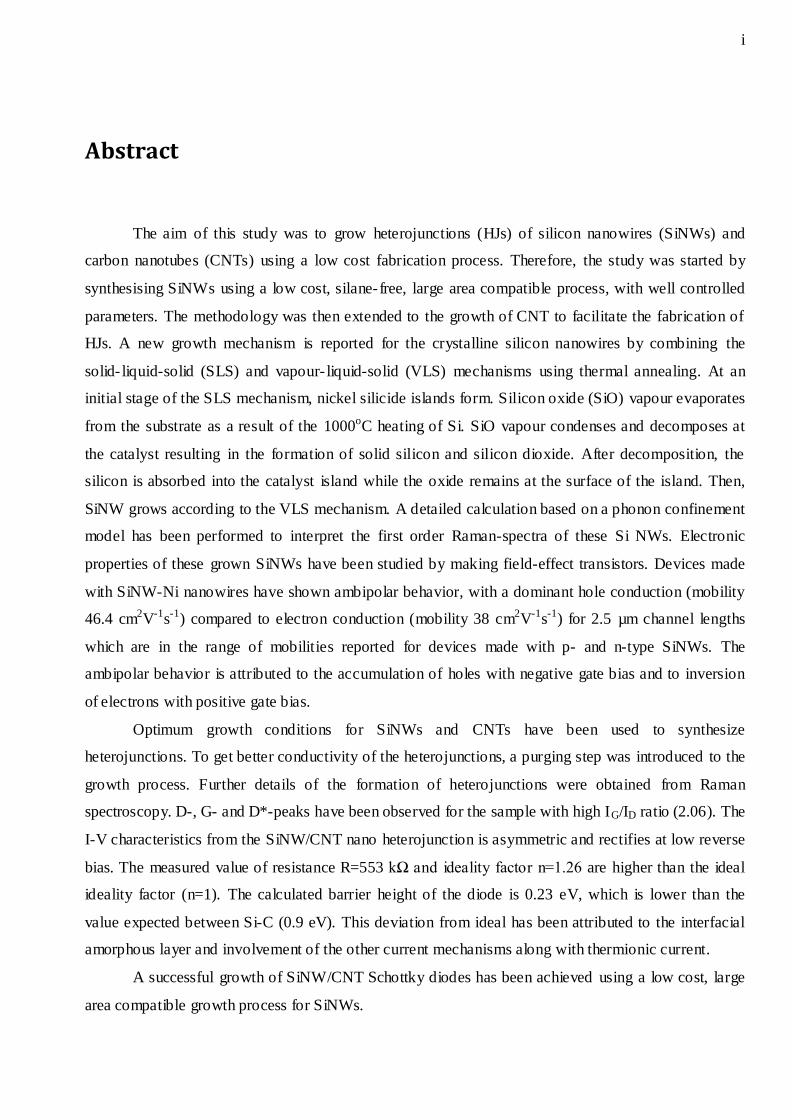
Abstract
The aim of this study was to grow heterojunctions (HJs) of silicon nanowires (SiNWs) and
carbon nanotubes (CNTs) using a low cost fabrication process. Therefore, the study was started by
synthesising SiNWs using a low cost, silane-free, large area compatible process, with well controlled
parameters. The methodology was then extended to the growth of CNT to facilitate the fabrication of
HJs. A new growth mechanism is reported for the crystalline silicon nanowires by combining the
solid- liquid-solid (SLS) and vapour- liquid-solid (VLS) mechanisms using thermal annealing. At an
initial stage of the SLS mechanism, nickel silicide islands form. Silicon oxide (SiO) vapour evaporates
from the substrate as a result of the 1000oC heating of Si. SiO vapour condenses and decomposes at
the catalyst resulting in the formation of solid silicon and silicon dioxide. After decomposition, the
silicon is absorbed into the catalyst island while the oxide remains at the surface of the island. Then,
SiNW grows according to the VLS mechanism. A detailed calculation based on a phonon confinement
model has been performed to interpret the first order Raman-spectra of these Si NWs. Electronic
properties of these grown SiNWs have been studied by making field-effect transistors. Devices made
with SiNW-Ni nanowires have shown ambipolar behavior, with a dominant hole conduction (mobility
46.4 cm2V-1s-1) compared to electron conduction (mobility 38 cm2V-1s-1) for 2.5 µm channel lengths
which are in the range of mobilities reported for devices made with p- and n-type SiNWs. The
ambipolar behavior is attributed to the accumulation of holes with negative gate bias and to inversion
of electrons with positive gate bias.
Optimum growth conditions for SiNWs and CNTs have been used to synthesize
heterojunctions. To get better conductivity of the heterojunctions, a purging step was introduced to the
growth process. Further details of the formation of heterojunctions were obtained from Raman
spectroscopy. D-, G- and D*-peaks have been observed for the sample with high IG/ID ratio (2.06). The
I-V characteristics from the SiNW/CNT nano heterojunction is asymmetric and rectifies at low reverse
bias. The measured value of resistance R=553 kΩ and ideality factor n=1.26 are higher than the ideal
ideality factor (n=1). The calculated barrier height of the diode is 0.23 eV, which is lower than the
value expected between Si-C (0.9 eV). This deviation from ideal has been attributed to the interfacial
amorphous layer and involvement of the other current mechanisms along with thermionic current.
A successful growth of SiNW/CNT Schottky diodes has been achieved using a low cost, large
area compatible growth process for SiNWs.

ii
Acknowledgements
The writing of this thesis is the most significant milestone in my life. I couldn‘t have come this
far without the assistance of many individuals and I want to express my deepest appreciation to them.
I would like to express my heartiest gratitude to my supervisor Prof. S. Ravi P. Silva, who has
introduced me to a cutting-edge research topic and provided me precious ideas, which made the work
possible. His wisdom, knowledge and commitment to the highest standards has inspired and motivated
me.
I would like to express my appreciation to Dr. Jose J. Anguita, for providing his support and
guidance for the growth, Dr. Vlad Stolojan, for conducting TEM and EELS for the samples and also
for advice and critiques on the Raman discussions.
I would like to thank Dr. Simon Henley, for his advice on the work, Dr. David Carey, for
discussions on Raman analysis and reviewing the thesis. Dr. David Cox for providing his support on
work carried out on the SEM and discussions on the growth process.
I would also like to thank Dr. Fumitika Ohashi, Dr. Anto Regis Inigo, Dr. Cristina Giusca,
Dean Mansfield, John Underwood, Chris Buxey, Tony Corless and Dr. Martin Blissett for being very
helpful on and off research work. I am grateful to the Advanced Technology Institute and all its
members for making a helpful and enjoyable environment to work in.
I convey my thanks to EPSRC for providing financial support for the research.
I believe I owe deepest thanks to all the people in my entire family who have supported,
encouraged and believed in me, throughout my life and am very grateful to my parents. I couldn‘t have
started this project without all they have done for me.
Last but not least, I am greatly indebted to my husband Ravi and my son Rushil, without them
this effort would have been worth nothing. They form the backbone and origin of my happiness. Their
love and support without any complaint or regret has enabled me to complete this PhD project. Thank
you to the one ―yet to be born‖ for giving me company while I finished thesis write-up.
Parul Sharma
May 2011
iii
Abbreviations
CNTs Carbon Nanotubes
CVD Chemical Vapour Deposition
EDXS Energy Dispersion X-ray Spectroscopy
EELS Electron Energy Loss Spectroscopy
ESEM Environmental Scanning Electron Microscopy
EFTEM Energy Filtered Transmission Electron Microscopy
ICP Inductively Coupled Plasma
MWNTs Multi-walled Carbon Nanotubes
NTs Nanotubes
OAG Oxide Assisted Growth
PECVD Plasma Enhanced Chemical Vapour Deposition
RIE Reactive Ion Etching
SEM Scanning Electron Microscopy
SiNPs Silicon Nanopillars
SiNWs Silicon Nanowires
SLS Solid- liquid-solid
STM Scanning Tunneling Microscopy
SWNT Single-walled Carbon Nanotubes
TEM Transmission Electron Microscopy
VLS Vapour- liquid-solid
iv
Contents
Abstract...................................................................................................................................................... i
Acknowledgements................................................................................................................................... ii
Abbreviations .......................................................................................................................................... iii
Contents................................................................................................................................................... iv
1. Introduction ..................................................................................................................................... 1
1.1 Why Heterojunctions are important? ......................................................................................... 1
1.2 Potential of SiNW/CNT Heterojunctions .................................................................................. 2
1.3 Research Aim ............................................................................................................................. 8
1.4 Layout of the Thesis................................................................................................................... 9
2 Literature Review ........................................................................................................................... 11
2.1 Silicon Nanowires .................................................................................................................... 11
2.1.1 Physical Properties of SiNWs........................................................................................... 13
2.1.2 Applications of SiNWs ..................................................................................................... 14
2.1.3 Silicon Nanowire Growth ................................................................................................. 18
2.2 Carbon Nanotubes.................................................................................................................... 22
2.2.1 Physical Properties of CNTs............................................................................................. 25
2.2.2 Applications of CNTs ....................................................................................................... 25
2.2.3 Carbon Nanotube Growth ................................................................................................. 27
2.3 Heterojunctions ........................................................................................................................ 28
2.3.1 Band Diagram of the Heterojunction................................................................................ 29
2.3.2 Metal/Semiconductor (MS) Junctions .............................................................................. 32
2.4 Electrical Characterization of Nano Schottky Diodes ............................................................. 35
2.4.1 Thermionic Field Emission Theory .................................................................................. 38
2.4.2 Schottky Diode Parameter Extraction .............................................................................. 41
2.5 Possible growth mechanism of SiNW/CNT HJ ....................................................................... 44
2.5.1 Growth Mechanism for bottom-up growth ....................................................................... 44
2.5.2 Mechanisms for SiNWs growth from top-down approach ............................................... 48
2.6 Conclusions .............................................................................................................................. 49
3 Experimental Techniques .............................................................................................................. 50
v
3.1 Introduction .............................................................................................................................. 50
3.2 DC-Magnetron Sputtering System........................................................................................... 50
3.3 Thermal annealing Lenton furnace system .............................................................................. 51
3.4 PECVD System........................................................................................................................ 52
3.5 Inductively Coupled Plasma (ICP-RIE) Etching ..................................................................... 54
3.6 Photolithography ...................................................................................................................... 56
3.7 Scanning Electron Microscopy ................................................................................................ 58
3.8 Transmission Electron Microscopy ......................................................................................... 60
3.9 Raman Spectroscopy................................................................................................................ 61
3.10 Summary............................................................................................................................... 65
4 Silicon Nanowires Synthesis ......................................................................................................... 66
4.1 Silicon oxide nanowire growth ................................................................................................ 67
4.1.1 Metal Coating ................................................................................................................... 67
4.1.2 Experimental Conditions .................................................................................................. 69
4.1.3 Results and Discussion ..................................................................................................... 70
4.2 Crystalline core-clad SiNWs growth ....................................................................................... 89
4.2.1 Experimental Section ........................................................................................................ 89
4.2.2 Results and Discussion ..................................................................................................... 90
4.3 Silicon nanopillars fabrication through etching ..................................................................... 102
4.3.1 Mask formation............................................................................................................... 102
4.3.2 ICP Etching..................................................................................................................... 104
4.3.3 Results and Discussion ................................................................................................... 105
4.4 Electronic Properties .............................................................................................................. 108
4.4.1 Field-effect transistor Fabrication................................................................................... 108
4.4.2 Device Physics ................................................................................................................ 109
4.4.3 Device Measurements..................................................................................................... 111
4.5 Conclusions ............................................................................................................................ 118
5 Carbon Nanotube Synthesis ........................................................................................................ 121
5.1 CNT growth with methane as carbon feedstock .................................................................... 121
5.1.1 Experimental Condition .................................................................................................. 123
5.1.2 Results and Discussion ................................................................................................... 124
5.2 CNT growth with acetylene as carbon feedstock................................................................... 135
5.2.1 Experimental Condition .................................................................................................. 135
5.2.2 Results and Discussion ................................................................................................... 136
vi
5.3 Electrical Characterization of CNTs ...................................................................................... 139
5.4 Conclusions ............................................................................................................................ 143
6 SiNW/CNT heterojunctions Growth ........................................................................................... 144
6.1 Bottom-up Approach.............................................................................................................. 144
6.1.1 Optimum conditions for SiNW growth .......................................................................... 144
6.1.2 Results and Discussion ................................................................................................... 146
6.2 Top-down Approach .............................................................................................................. 160
6.2.1 Experimental Conditions ................................................................................................ 160
6.2.2 Results and Discussion ................................................................................................... 161
6.3 Real Interfaces........................................................................................................................ 165
6.4 Conclusions ............................................................................................................................ 166
7 Summary and Conclusion ........................................................................................................... 167
7.1 Silicon Nanowire Growth ...................................................................................................... 167
7.2 Carbon Nanotube Growth ...................................................................................................... 167
7.3 SiNW/CNT heterojunctions Growth...................................................................................... 169
7.4 Proposed Future Work ........................................................................................................... 169
List of Publications .............................................................................................................................. 172
Bibliography ......................................................................................................................................... 173
1
1. Introduction
Nanoelectronics have fascinated scientists due to its fundamental and technological interest.
Nanoparticles can exhibit energy confinement in quantum states. One of the goals for nanoelectronics
is to achieve higher performance devices in higher densities compared to conventional semiconductor
technology.
The large scope of bulk heterojunctions have drawn interest in the study of one-dimensional
(1D) heterojunctions (HJs). These are formed at the point of contact between 1D nanostructures e.g.
nanorods, nanowires, nanoribbons, nanobelts etc. They provide the facility to enhance the device
properties of systems made from only one material. The transport of electrons and holes in materials
can be controlled by varying the composition of materials through band engineering. These HJs have
applications in photonics and electronics (Einspruch and Frensley 1994) as functional and
interconnecting elements, and could be useful in making light-emitting diodes ( ak et al.
2005; Wang, Cole et al. 2007) as well as single electron transistors (Thelander, Martensson et al.
2003).
1.1 Why are Heterojunctions important?
Nanocircuits are extremely sensitive to their surroundings, and have potential electronic
applications (Hu, Odom et al. 1999; Zhang, Ichihashi et al. 1999). This makes them highly suitable for
detecting molecules such as gases (Weichsel and et al. 2005; Tsai, Chen et al. 2007). Therefore, they
have great appeal to engineer them from the nanoscale to combine the fields of physical sciences,
engineering and the life sciences. There is a wide selection of building blocks in 1D nanostructures for
nanocircuits which has fascinated researchers due to their optoelectronic, electrochemical, and
electromechanical properties. For the development of nanocircuits, an appropriate current-voltage
characteristic should be obtained by controlling the potential barrier between adjacent constituents.
2
This leads towards the synthesis and design of various multi component 1D materials. These 1D multi
component materials contain heterojunctions such as p-n junctions, metal-semiconductor junctions or
metal-oxide-semiconductor junctions. These 1D heterojunctions give the combined benefit of the 1D
material with the unique features of heterojunctions. Higher device density with vastly different
properties compared to their bulk counterpart is a feature of 1D structures which leads to smaller and
more portable devices. It is possible to avoid lattice mismatches in nano heterojunctions of two highly
different lattice constants where conventional bulk heterojunctions are subject to large misfit
dislocations which can be detrimental to the electronic performances of the devices.
1.2 Potential of SiNW/CNT Heterojunctions
Diverse 1D heterojunctions have been explored, e.g. semiconductor/semiconductor (Wang,
Cole et al. 2007), semiconductor/metal (Wu and et al. 2007; Yang, Meng et al. 2007), metal/metal,
carbon/carbon(Luo, Xing et al. 2006), carbon/semiconductor (Hu, Odom et al. 1999) and carbon/metal
(Luo, Xing et al. 2006), where carbon can be in the form of carbon nanotubes, graphene, diamond or
amorphous carbon. Wang, Cole et al. (2007) have grown zinc oxide Nanowire (NW) / p-gallium
nitride HJ LEDs showing electroluminescence (EL) under both forward and reverse bias. Forward bias
emission shows that holes are injected from the GaN and combine with electrons in zinc oxide.
Reverse bias EL shows that electrons and holes combine in p-GaN, indicating a difference from
forward bias condition.
3
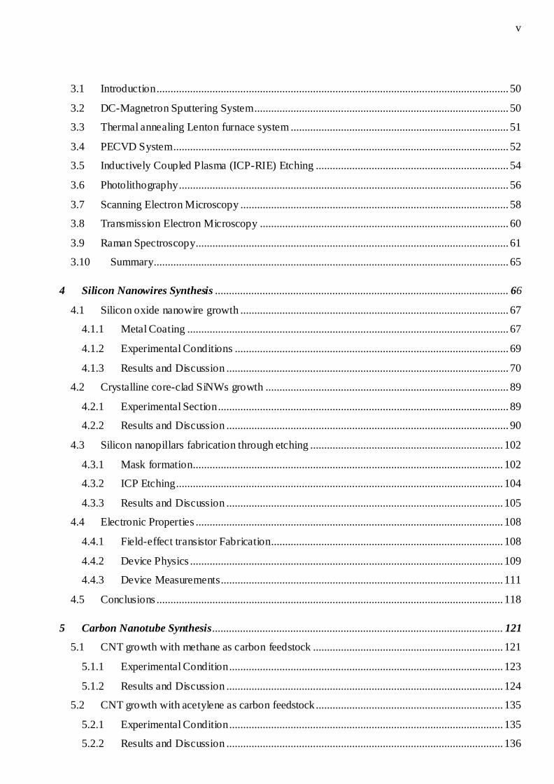
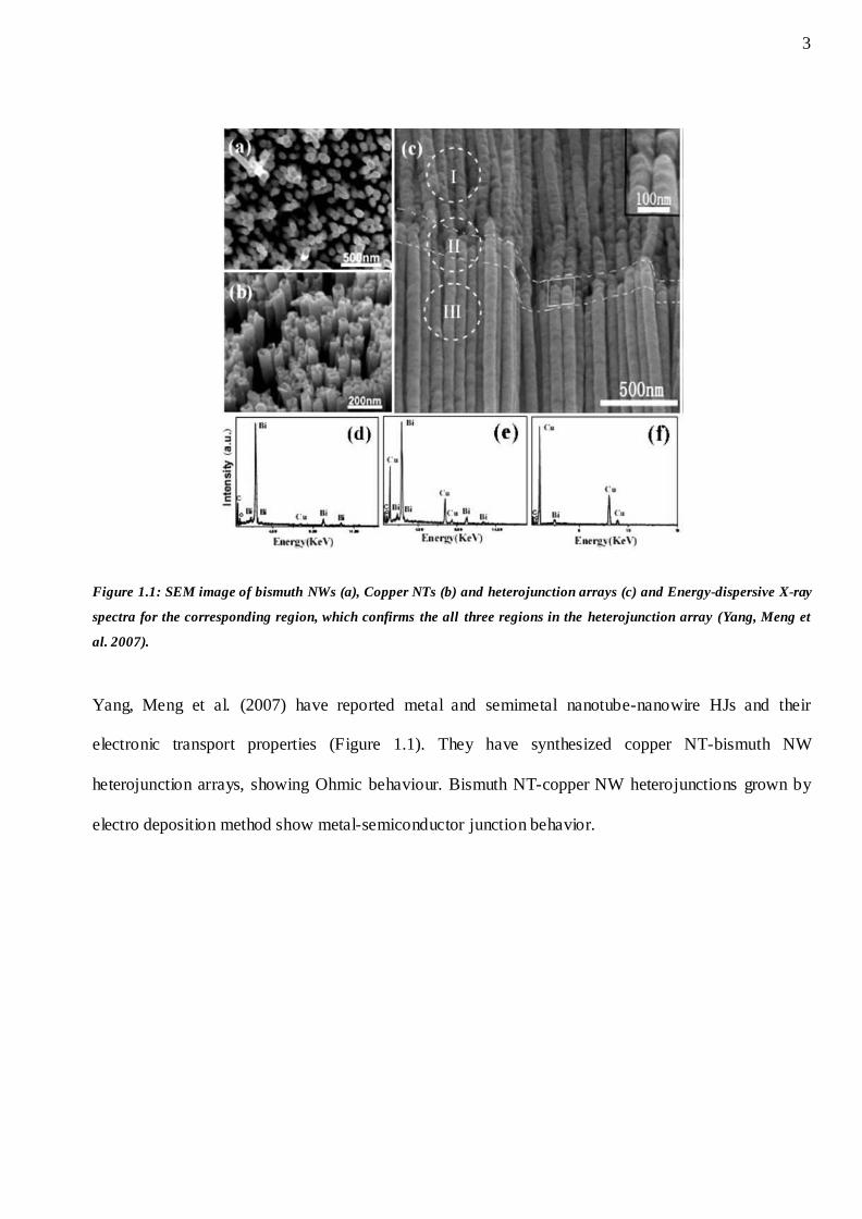
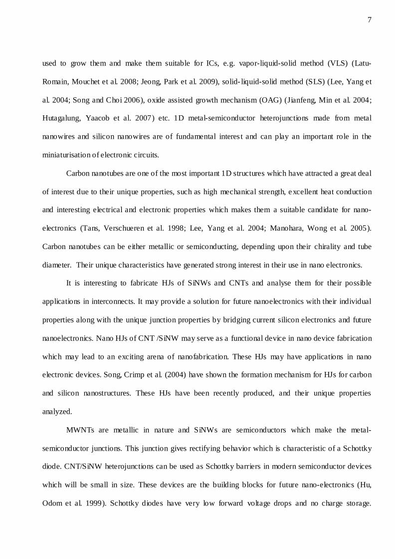
Figure 1.1: SEM image of bismuth NWs (a), Copper NTs (b) and heterojunction arrays (c) and Energy-dispersive X-ray
spectra for the corresponding region, which confirms the all three regions in the heterojunction array (Yang, Meng et
al. 2007).
Yang, Meng et al. (2007) have reported metal and semimetal nanotube-nanowire HJs and their
electronic transport properties (Figure 1.1). They have synthesized copper NT-bismuth NW
heterojunction arrays, showing Ohmic behaviour. Bismuth NT-copper NW heterojunctions grown by
electro deposition method show metal-semiconductor junction behavior.
4
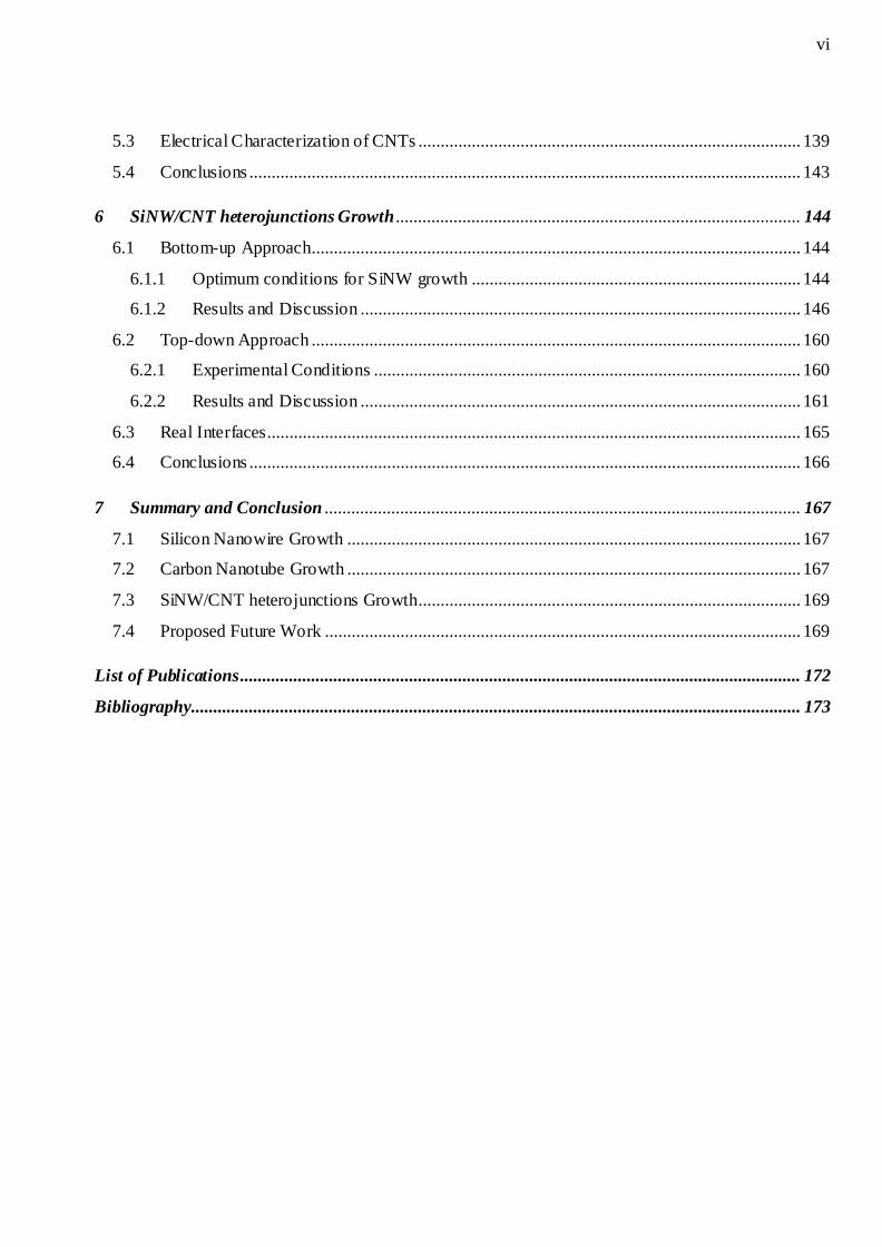
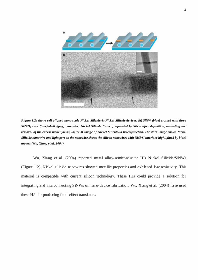
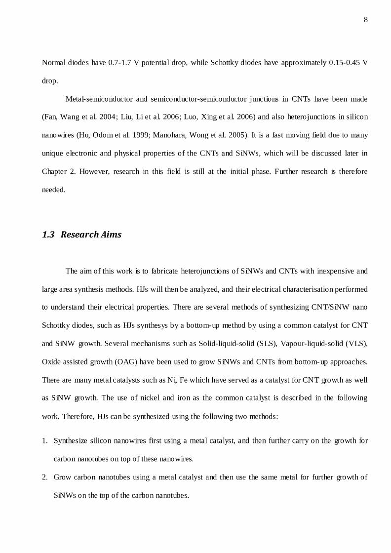
Figure 1.2: shows self aligned nano-scale Nickel Silicide-Si-Nickel Silicide devices; (a) SiNW (blue) crossed with three
Si/SiO2 core (blue)-shell (grey) nanowire; Nickel Silicide (brown) separated by SiNW after deposition, annealing and
removal of the excess nickel yields, (b) TEM image of Nickel Silicide/Si heterojunction. The dark image shows Nickel
Silicide nanowire and light part on the nanowire shows the silicon nanowires with NiSi/Si interface highlighted by black
arrows (Wu, Xiang et al. 2004).
Wu, Xiang et al. (2004) reported metal alloy-semiconductor HJs Nickel Silicide/SiNWs
(Figure 1.2). Nickel silicide nanowires showed metallic properties and exhibited low resistivity. This
material is compatible with current silicon technology. These HJs could provide a solution for
integrating and interconnecting SiNWs on nano-device fabrication. Wu, Xiang et al. (2004) have used
these HJs for producing field-effect transistors.
5
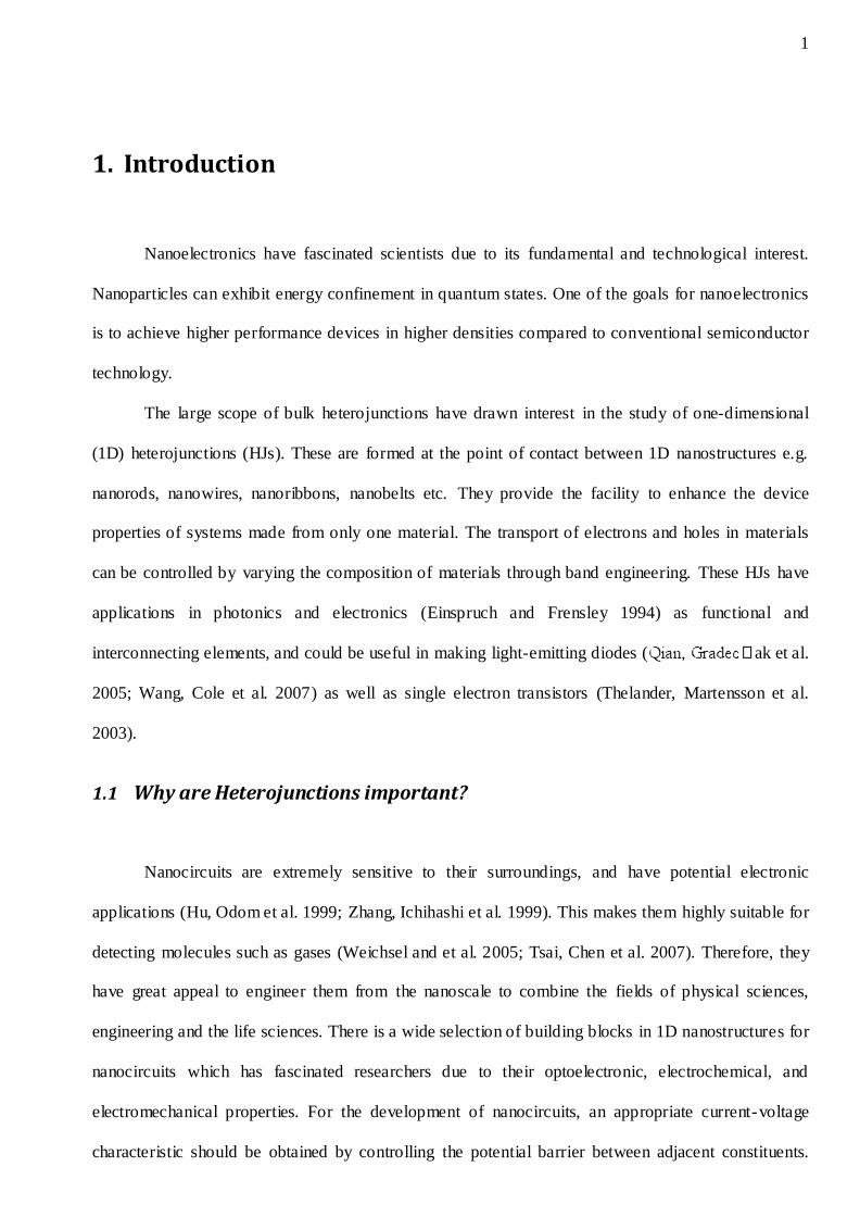
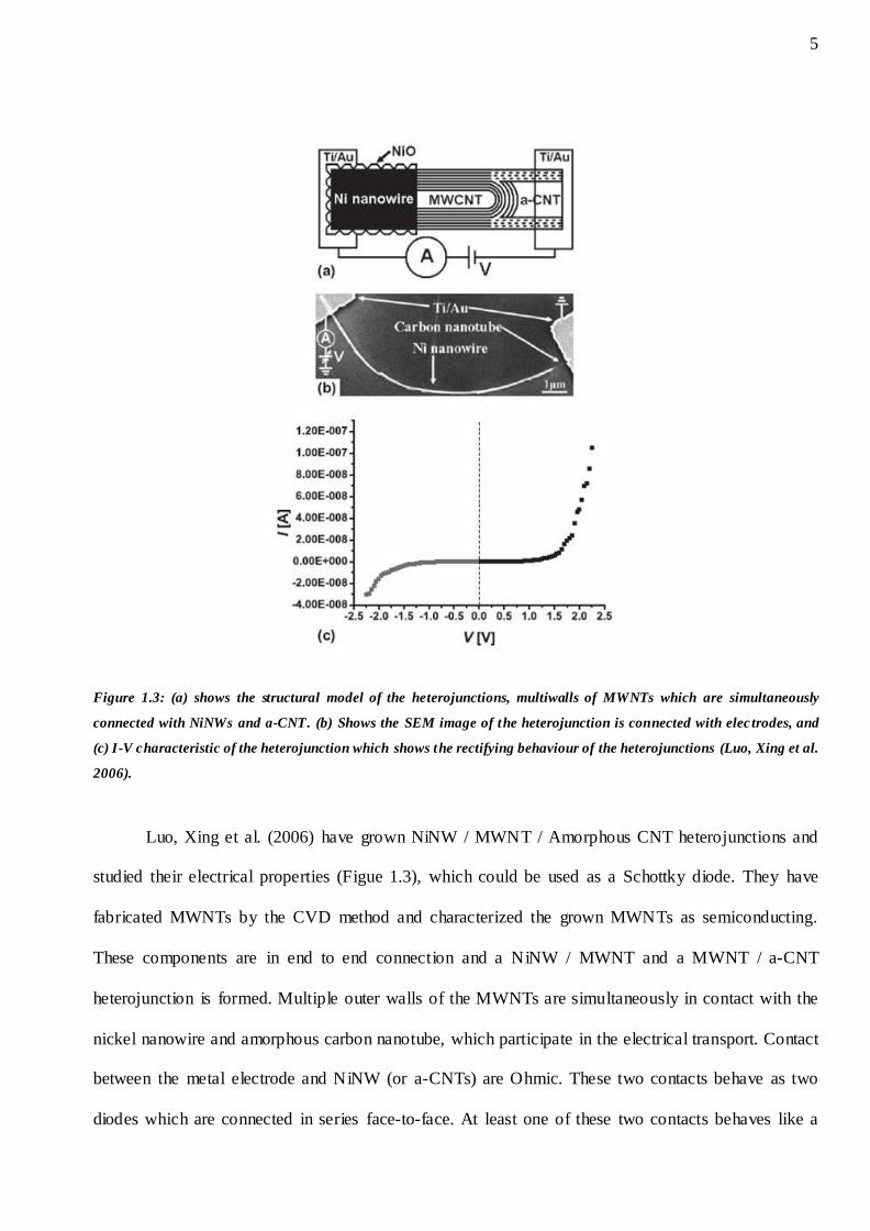
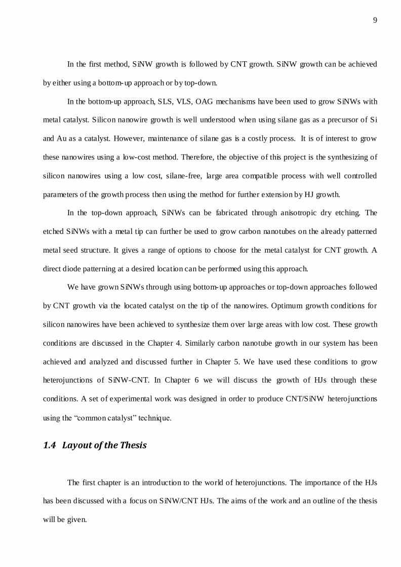
Figure 1.3: (a) shows the structural model of the heterojunctions, multiwalls of MWNTs which are simultaneously
connected with NiNWs and a-CNT. (b) Shows the SEM image of the heterojunction is connected with elec trodes, and
(c) I-V characteristic of the heterojunction which shows the rectifying behaviour of the heterojunctions (Luo, Xing et al.
2006).
Luo, Xing et al. (2006) have grown NiNW / MWNT / Amorphous CNT heterojunctions and
studied their electrical properties (Figue 1.3), which could be used as a Schottky diode. They have
fabricated MWNTs by the CVD method and characterized the grown MWNTs as semiconducting.
These components are in end to end connection and a NiNW / MWNT and a MWNT / a-CNT
heterojunction is formed. Multiple outer walls of the MWNTs are simultaneously in contact with the
nickel nanowire and amorphous carbon nanotube, which participate in the electrical transport. Contact
between the metal electrode and NiNW (or a-CNTs) are Ohmic. These two contacts behave as two
diodes which are connected in series face-to-face. At least one of these two contacts behaves like a
6
nearly ideal Schottky diode and obeys thermionic emission theory, wherein only image force lowers
the Schottky barrier.
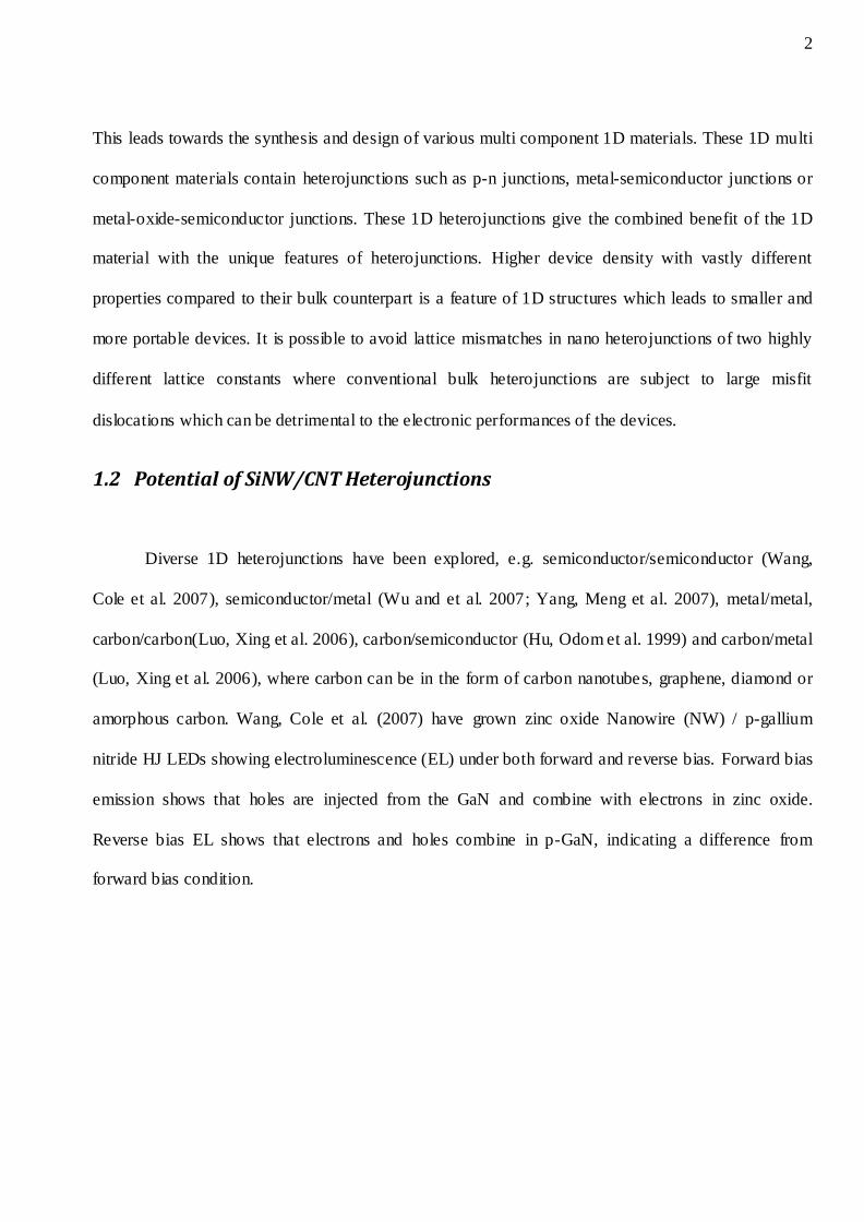
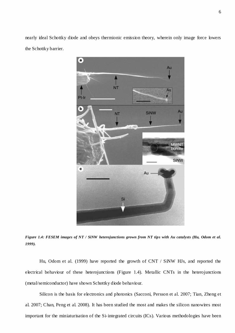
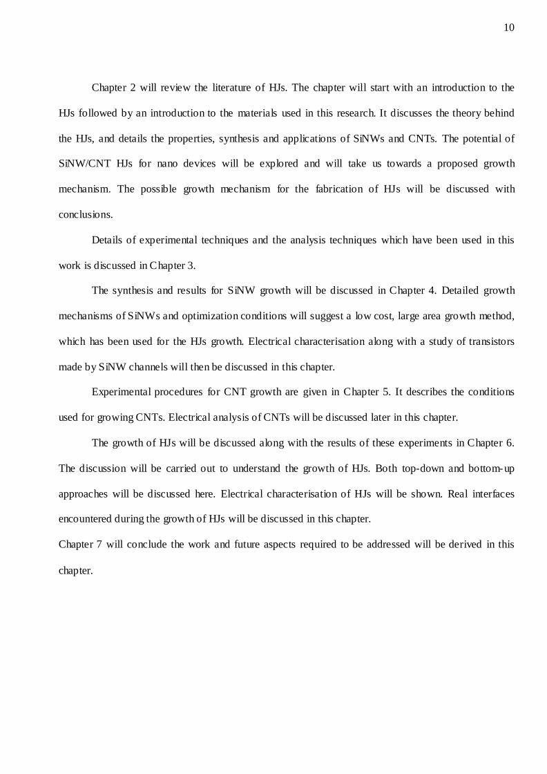
Figure 1.4: FESEM images of NT / SiNW heterojunctions grown from NT tips with Au catalysts (Hu, Odom et al.
1999).
Hu, Odom et al. (1999) have reported the growth of CNT / SiNW HJs, and reported the
electrical behaviour of these heterojunctions (Figure 1.4). Metallic CNTs in the heterojunctions
(metal/semiconductor) have shown Schottky diode behaviour.
Silicon is the basis for electronics and photonics (Sacconi, Persson et al. 2007; Tian, Zheng et
al. 2007; Chan, Peng et al. 2008). It has been studied the most and makes the silicon nanowires most
important for the miniaturisation of the Si- integrated circuits (ICs). Various methodologies have been
7
used to grow them and make them suitable for ICs, e.g. vapor-liquid-solid method (VLS) (Latu-
Romain, Mouchet et al. 2008; Jeong, Park et al. 2009), solid- liquid-solid method (SLS) (Lee, Yang et
al. 2004; Song and Choi 2006), oxide assisted growth mechanism (OAG) (Jianfeng, Min et al. 2004;
Hutagalung, Yaacob et al. 2007) etc. 1D metal-semiconductor heterojunctions made from metal
nanowires and silicon nanowires are of fundamental interes t and can play an important role in the
miniaturisation of electronic circuits.
Carbon nanotubes are one of the most important 1D structures which have attracted a great deal
of interest due to their unique properties, such as high mechanical strength, excellent heat conduction
and interesting electrical and electronic properties which makes them a suitable candidate for nano-
electronics (Tans, Verschueren et al. 1998; Lee, Yang et al. 2004; Manohara, Wong et al. 2005).
Carbon nanotubes can be either metallic or semiconducting, depending upon their chirality and tube
diameter. Their unique characteristics have generated strong interest in their use in nano electronics.
It is interesting to fabricate HJs of SiNWs and CNTs and analyse them for their possible
applications in interconnects. It may provide a solution for future nanoelectronics with their individual
properties along with the unique junction properties by bridging current silicon electronics and future
nanoelectronics. Nano HJs of CNT /SiNW may serve as a functional device in nano device fabrication
which may lead to an exciting arena of nanofabrication. These HJs may have applications in nano
electronic devices. Song, Crimp et al. (2004) have shown the formation mechanism for HJs for carbon
and silicon nanostructures. These HJs have been recently produced, and their unique properties
analyzed.
MWNTs are metallic in nature and SiNWs are semiconductors which make the metal-
semiconductor junctions. This junction gives rectifying behavior which is characteristic of a Schottky
diode. CNT/SiNW heterojunctions can be used as Schottky barriers in modern semiconductor devices
which will be small in size. These devices are the building blocks for future nano-electronics (Hu,
Odom et al. 1999). Schottky diodes have very low forward voltage drops and no charge storage.
8
Normal diodes have 0.7-1.7 V potential drop, while Schottky diodes have approximately 0.15-0.45 V
drop.
Metal-semiconductor and semiconductor-semiconductor junctions in CNTs have been made
(Fan, Wang et al. 2004; Liu, Li et al. 2006; Luo, Xing et al. 2006) and also heterojunctions in silicon
nanowires (Hu, Odom et al. 1999; Manohara, Wong et al. 2005). It is a fast moving field due to many
unique electronic and physical properties of the CNTs and SiNWs, which will be discussed later in
Chapter 2. However, research in this field is still at the initial phase. Further research is therefore
needed.
1.3 Research Aims
The aim of this work is to fabricate heterojunctions of SiNWs and CNTs with inexpensive and
large area synthesis methods. HJs will then be analyzed, and their electrical characterisation performed
to understand their electrical properties. There are several methods of synthesizing CNT/SiNW nano
Schottky diodes, such as HJs synthesys by a bottom-up method by using a common catalyst for CNT
and SiNW growth. Several mechanisms such as Solid-liquid-solid (SLS), Vapour-liquid-solid (VLS),
Oxide assisted growth (OAG) have been used to grow SiNWs and CNTs from bottom-up approaches.
There are many metal catalysts such as Ni, Fe which have served as a catalyst for CNT growth as well
as SiNW growth. The use of nickel and iron as the common catalyst is described in the following
work. Therefore, HJs can be synthesized using the following two methods:
1. Synthesize silicon nanowires first using a metal catalyst, and then further carry on the growth for
carbon nanotubes on top of these nanowires.
2. Grow carbon nanotubes using a metal catalyst and then use the same metal for further growth of
SiNWs on the top of the carbon nanotubes.
9
In the first method, SiNW growth is followed by CNT growth. SiNW growth can be achieved
by either using a bottom-up approach or by top-down.
In the bottom-up approach, SLS, VLS, OAG mechanisms have been used to grow SiNWs with
metal catalyst. Silicon nanowire growth is well understood when using silane gas as a precursor of Si
and Au as a catalyst. However, maintenance of silane gas is a costly process. It is of interest to grow
these nanowires using a low-cost method. Therefore, the objective of this project is the synthesizing of
silicon nanowires using a low cost, silane-free, large area compatible process with well controlled
parameters of the growth process then using the method for further extension by HJ growth.
In the top-down approach, SiNWs can be fabricated through anisotropic dry etching. The
etched SiNWs with a metal tip can further be used to grow carbon nanotubes on the already patterned
metal seed structure. It gives a range of options to choose for the metal catalyst for CNT growth. A
direct diode patterning at a desired location can be performed using this approach.
We have grown SiNWs through using bottom-up approaches or top-down approaches followed
by CNT growth via the located catalyst on the tip of the nanowires. Optimum growth conditions for
silicon nanowires have been achieved to synthesize them over large areas with low cost. These growth
conditions are discussed in the Chapter 4. Similarly carbon nanotube growth in our system has been
achieved and analyzed and discussed further in Chapter 5. We have used these conditions to grow
heterojunctions of SiNW-CNT. In Chapter 6 we will discuss the growth of HJs through these
conditions. A set of experimental work was designed in order to produce CNT/SiNW heterojunctions
using the ―common catalyst‖ technique.
1.4 Layout of the Thesis
The first chapter is an introduction to the world of heterojunctions. The importance of the HJs
has been discussed with a focus on SiNW/CNT HJs. The aims of the work and an outline of the thesis
will be given.
10
Chapter 2 will review the literature of HJs. The chapter will start with an introduction to the
HJs followed by an introduction to the materials used in this research. It discusses the theory behind
the HJs, and details the properties, synthesis and applications of SiNWs and CNTs. The potential of
SiNW/CNT HJs for nano devices will be explored and will take us towards a proposed growth
mechanism. The possible growth mechanism for the fabrication of HJs will be discussed with
conclusions.
Details of experimental techniques and the analysis techniques which have been used in this
work is discussed in Chapter 3.
The synthesis and results for SiNW growth will be discussed in Chapter 4. Detailed growth
mechanisms of SiNWs and optimization conditions will suggest a low cost, large area growth method,
which has been used for the HJs growth. Electrical characterisation along with a study of transistors
made by SiNW channels will then be discussed in this chapter.
Experimental procedures for CNT growth are given in Chapter 5. It describes the conditions
used for growing CNTs. Electrical analysis of CNTs will be discussed later in this chapter.
The growth of HJs will be discussed along with the results of these experiments in Chapter 6.
The discussion will be carried out to understand the growth of HJs. Both top-down and bottom-up
approaches will be discussed here. Electrical characterisation of HJs will be shown. Real interfaces
encountered during the growth of HJs will be discussed in this chapter.
Chapter 7 will conclude the work and future aspects required to be addressed will be derived in this
chapter.
11
2 Literature Review
This chapter introduces the literature available on heterojunctions of silicon nanowire and
carbon nanotubes. First, the theory of the materials used in this study is presented. Then this chapter
will focus on the electrical characterisation of nano heterojunctions and Schottky diode parameter
extraction. The possible growth mechanisms will be discussed at the end of this Chapter.
Introduction to the materials used in this study
2.1 Silicon Nanowires
Nanostructures such as nanotubes and nanowires offer unique access to low-dimensional
physics. Nanowires could be important, as they can be considered the building blocks of a technology
which harnesses the quantum size effects for useful device applications. Device integration densities
too can be optimized. Such one-dimensional nano-materials can play a key role in nanotechnology, as
well as provide model systems to demonstrate quantum size effects. Silicon-based nanowires including
silicon, silicate and silicide nanowires are particularly attractive due to the central role of silicon to the
semiconductor industry. Potential applications include the field of photonics, photovoltaic,
interconnects, sensors and nano-electromechanical systems.
For SiNWs, the carrier type and concentration can be controlled by doping, as in bulk silicon.
Furthermore silicon turns into a direct-band-gap semiconductor at nanometer size, due to quantum
confinement, opening an entirely new field of optoelectronic applications for such nano silicon-based
devices. But SiNWs having extremely small diameters show indirect band gaps (Scheel, Reich et al.
2005). This suggests using medium sized nanowires for the optical applications. Si-based nanowires
have shown stable electroluminescent devices at room temperature. Si-based nanowires have also
shown efficiency enhancement in test photovoltaic applications, arising from the enhanced optical
12
absorption of this nanostructured form of silicon. It is clear that Si-based nanowire research has led to
a clear improvement in device performance in terms of efficiency. However, there is still much scope
in developing understanding into the growth and behaviour of this material before viable device
production becomes possible.
At the nano-scale, quantum-confinement effects are important, which affects the properties of
materials. So, it is important to see the quantum-confinement effects and exciton effects at the nano-
scale, which affects the optical properties of the nanowires. The orientation of the SiNWs grown
depends on the diameter of the nanowires. Smaller SiNWs whose diameter range from 3 nm to 10 nm,
are grown primarily along the (110) direction. Also medium SiNWs whose diameter ranges from 10
nm to 20 nm, grow primarily along the (112) direction and large SiNWs whose diameter ranges from
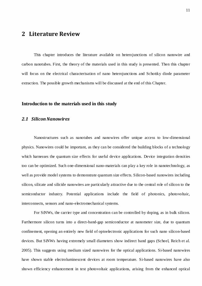
20 nm to 30 nm, grown primarily along the (111) direction (Marsen and Sattler 1999).
Figure 2.1: Schematic presentations of small diameter silicon nanowires (a) tetrahedral (top), (b) Si34-clathrate, (c)
Si46-clathrate and (d) polycrystalline types of nanowires (Marsen and Sattler 1999).
Several possible structures for SiNWs have been reported. These include fullerene like cage
structure (clathrate), tetrahedral structures and polycrystalline nanowires (Marsen and Sattler 1999;
Hofmann, Ducati et al. 2003; Ponomareva, Menon et al. 2005) as shown in figure 2.1.
13
The surface of SiNWs is easily oxidized in air due to a high density of dangling bonds at the
surface.
2.1.1 Physical Properties of SiNWs
SiNWs have one free direction in which the electrical carriers can flow. Their physical
properties are significantly different from those in bulk silicon, as explained below
2.1.1.1 Electronic and Optical Properties
SiNWs show quantum confinement (Law, Goldberger, & Yang, 2004). This confinement is
manifested as a change in the band gap from the bulk material. The band gap is directly related to the
diameter of the nanowires (Ma, Lee et al. 2003)
(2.1)
where, d is the diameter of the nanowire.
SiNWs have exhibited band gap variations from 1.1 to 3.95 eV with diameters ranging
from 7 nm to 1.3 nm, respectively (Yun, Rivas et al. 2005). The electronic properties such as the band
gap, valley splitting and effective mass are also functions of the diameter (Sacconi, Persson et al.
2007). These affect the transport properties of the nanowires (Saitta, Buda et al. 1996). Hydrogen and
oxygen terminated SiNWs have been studied to gain an understanding of their optical and electronic
properties. Confinement in SiNWs render them optically active (direct band gap), and are independent
of their specific orientation (Ponomareva, Menon et al. 2005). Quantum confinement in nanowires
could play an important role in photovoltaic devices. SiNWs could also be used as light emitting
diodes and lasers at small diameters.
14
2.1.1.2 Thermal and Mechanical Properties
SiNWs could have applications in nano-scale thermoelectric power generators (Paulo, Bokor et
al. 2005; Chen 2007). Therefore, it is important to study their thermal conductivity. Thin SiNWs,
having diameters between 1.4 and 8.3 nm have been studied. As the nanowire diameter decreases, the
surface to volume ratio increases, which increases the surface scattering effects. This decrea ses the
thermal conductivity of the nanowires. While at very small diameter (<1.5nm), quantum confinement
effect occur and these increase the thermal conductivity (Paulo, Bokor et al. 2005). The values of
Young‘s Modulus for SiNWs were similar to that for bulk Si (Chen 2007). The values of Young‘s
modulus were estimated to be 186 and 207 GPa respectively, for single- and double- clamped SiNWs.
The values are close to the bulk value of 169 GPa for Si(111).
2.1.2 Applications of SiNWs
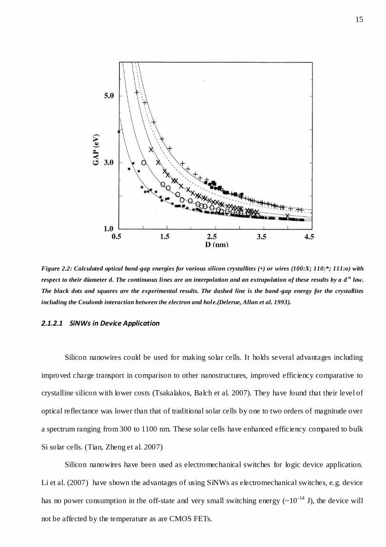
Figure 2.2 shows the dependency of the band gap energy with diameter of silicon nanowires.
The band gap increases with decreasing diameter of the wires, which greatly enhances at low diameter,
introducing quantum confinement. Band-gaps ranging from 1.1 eV for 7 nm to 3.5 eV for 1.3 nm,
demonstrates the quantum size effect in the silicon nanowires. (Delerue, Allan et al. 1993)
15
Figure 2.2: Calculated optical band-gap energies for various silicon crystallites (+) or wires (100:X; 110:*; 111:o) with
respect to their diameter d. The continuous lines are an interpolation and an extrapolation of these results by a d-n
law.
The black dots and squares are the experimental results. The dashed line is the band -gap energy for the crystallites
including the Coulomb interaction between the electron and hole.(Delerue, Allan et al. 1993).
2.1.2.1 SiNWs in Device Application
Silicon nanowires could be used for making solar cells. It holds several advantages including
improved charge transport in comparison to other nanostructures, improved efficiency comparative to
crystalline silicon with lower costs (Tsakalakos, Balch et al. 2007). They have found that their level of
optical reflectance was lower than that of traditional solar cells by one to two orders of magnitude over
a spectrum ranging from 300 to 1100 nm. These solar cells have enhanced efficiency compared to bulk
Si solar cells. (Tian, Zheng et al. 2007)
Silicon nanowires have been used as electromechanical switches for logic device application.
Li et al. (2007) have shown the advantages of using SiNWs as electromechanical switches, e.g. device
has no power consumption in the off-state and very small switching energy (~10-14 J), the device will
not be affected by the temperature as are CMOS FETs.
16
Silicon nanowire field effect transistors (SiNWFETs) have been fabricated, where direct metal
contacts formed the source and the drain. Traditional FET structures have p-n doping. Formation of the
source-doping and drain-doping and metal contacts requires complex process steps. SiNWs with
Schottky contacts can be used as enhancement-mode FETs (Koo and et al. 2005). These provide a
number of advantages over the traditional FETs, e.g. simple and low temperature processing, the
elimination of doping and subsequent activation steps. This shows excellent enhancement-mode
characteristics and a high on/off current ratio of up to ≈107 (Koo and et al. 2005). It showed improved
thermal emission leakage (≈6*10-13 A/mm) with 60nm channel width and 3 to 4 orders of magnitude
improvement in the on/off current ratio compared to traditional FETs (Koo and et al. 2005). Overall
device performance was improved compared to traditional FETs.
2.1.2.2 SiNWs in Data storage technology
Nanowires could play an essential role in future nanoscale electronics. Li et al. (2007) have
fabricated a non volatile memory device. A self-alignment technique is used to position the silicon
nanowires, which could allow for lower production cost than current flash memory cards. SiNW based
memory devices showed better stability at higher temperatures. (Li et al. 2007)
2.1.2.3 SiNWs in rechargeable Lithium-Ion batteries
Lithium-Ion battery capacity depends on the lithium holding capacity of the anode. Silicon is a
good candidate as the anode material in such batteries, due to its low discharge potential.
Theoretically, this would allow one to achieve the highest known theoretical charge capacity (4200
mAh g-1, (Boukamp et al. 1981). Silicon nanowire based Lithium-Ion batteries could boost battery life
10 times. In these batteries, the lithium ions react with silicon nanowires and make lithium silicide
which has much greater capacity. Chan, Peng et al. (2008) observed that when energy is used up, the
lithium silicide turns back into silicon, so batteries are rechargeable. Laïk, Eude et al. (2008) have used
17
silicon nanowires as electrodes for lithium-ion micro batteries. It increases the storage capacity with
growth temperature by a factor of three as the temperature varies from 525 to 575oC. (Boukamp, Lesh
et al. 1981)
2.1.2.4 SiNWs as UV LEDs and Lasers
Silicon being an indirect band-gap semiconductor is an inefficient emitter of light. Single
crystal Si nanowires have possible applications in UV LEDs and lasers (Pavesi, Dal Negro et al. 2000).
Single crystal SiNWs provide a wide band-gap, which gives a direct electronic transition with an
allowed electric dipole and short radioactive life time emission. Pavesi, Dal Negro et al. (2000) have
shown the stimulated emission and light amplification in Si nanostructures. They have seen optical
gain in Si waveguides. Population inversion is shown between the fundamental and a radiative state
associated with the nano-crystal + oxide interface. These results could be the route for a Si based laser.
2.1.2.5 SiNWs as efficient thermoelectric materials
Conductive materials generate thermoelectricity. When a temperature gradient is applied across
the materials, then a charge difference builds up between the hot and cold region of the material, as a
result of the electron diffusion between the hot and cold region. Thermoelectric materials can be used
to generate electricity, to cool the objects or to heat them. These materials could be used in cars for
power generators by utilizing heat from the exhaust gasses. Conversion efficiency can be improved by
lowering the thermal conductivity. Nanostructure materials interface with the flow of heat to enhance
the efficiency. The efficiency depends on the factor ZT of their material components. ZT is a function
of the Seebeck coefficient, electrical resistivity, thermal conductivity and absolute temperature. SiNWs
have potential application as thermoelectric materials. SiNWs have the same Seebeck coefficient and
electrical reisitivity values as bulk Si. But due to their small size, they can show a 100-fold reduction
in thermal conductivity, which gives ZT=0.60 at room temperature (Boukai, Bunimovich et al. 2008).
18
With reducing diameter it could be possible to achieve ZT values of 1 or greater, at room temperature.
Bulk Si is a poor thermoelectric material, while SiNWs with reduced thermal conductivity may be
useful thermoelectric materials (Boukai, Bunimovich et al. 2008).
2.1.2.6 SiNWs as chemical and biomedical Sensors
The sensitivity of the device increases as sensor dimensions shrink down to the size of the
analyte. Nanowire-based sensors are attractive due to their high surface to volume ratio. The sensing
mechanism for chemical species is based on the conductance of the nanowires. The conductivity of the
nanowires is changed as molecules absorb on the surface. Silicon nanowires are of particular interest
for sensing applications because Si has surface dangling bonds which can be effectively passivated and
become chemically modified. Silicon nanowires can be used as chemical and biosensors. Talin, Hunter
et. al. (2006) has shown the SiNW sensor will act as an FET with very high on/off ratio. When this
device is exposed to ammonia cyclohexane gas solutions containing nitrobenzene or phenol, the
threshold voltage shifts indicative of a charge transfer between the analytes and the nanowires is
recorded. (Elibol, Morisette et al. 2003; Talin, Hunter et al. 2006; Park, Li et al. 2007)
2.1.3 Silicon Nanowire Growth
There are several methods to synthesize SiNWs. These include Chemical Vapour Deposition
(CVD) (Kamins, Sharma et al. 2005), Laser ablation (Morales and Lieber 1998; Fukata, Oshima et al.
2005), thermal-evaporation (Wong, Yahaya et al. ; Song and Choi 2006), and solid-state growth from
silicon substrates.
The CVD process favours SiNW growth by the vapour- liquid-solid (VLS) mechanism when a
suitable catalyst is present (such as gold). This allows growth at comparatively low temperatures
(~400°C) due to the low eutectic temperature (363oC) of the gold-silicon alloy. Nanowires grown from
this method are single crystal. Typical gases Si2H6, SiH4, SiH2Cl2 and SiCl4 usually act as precursor
19
for growing SiNWs from CVD. Gold works as a catalyst which gives lower dissociation energy for the
decomposition of the silicon precursor gas. Sharma et al. (2004) have shown a dependency of the
silicon nanowire diameter on the thickness of the catalyst deposited and on the annealing conditions.
Laser ablation also uses the VLS mechanism. This method allows for high yields, takes
comparatively less growth time, and can give controlled growth with changing synthesis parameters.
But it does not allow for growth in large surface areas, which is important for making devices. A
suitable thermally pressed target is used for growth, which is placed in the chamber on the target plate.
A laser beam is used to vaporize the target at low pressure, and condenses on the substrate catalyst.
Fukata, Oshima et al. (2005) have grown silicon nanowires with Ni and Fe as catalysts. The diameter
and length of the nanowires decrease with decreasing laser power. Morales and Lieber (1998) have
grown silicon nanowires of diameters of 6 to 20 nm, and lengths ranging from 1 to 30 μm with laser
ablation. They used Au as a catalyst for their experiment.
Thermal evaporation is cost effective and doesn‘t use dangerous silane gas for growing the
SiNWs. But it uses high temperatures. The source material is vaporized which is transported by a
carrier gas. This transported material is deposited onto the substrate surface with catalyst deposit
where it condenses and the SLS growth mechanism takes place (Song & Choi, 2006). In some
methods, silicon wafer itself works as a source material. A metal catalyst is deposited onto the silicon
wafer and then kept in a furnace for thermal annealing and further nanowire growth (Wong, Yahaya et
al. 2005).
2.1.3.1 Catalyst used for SiNWs growth
Catalysts play an important role in the nanowire growth. The catalyst particle size determines
the nanowire diameter. Equilibrium phase diagrams can be used to select suitable catalyst materials
and growth conditions. There are many metals which are useful as catalysts for silicon nanowire
growth.
20
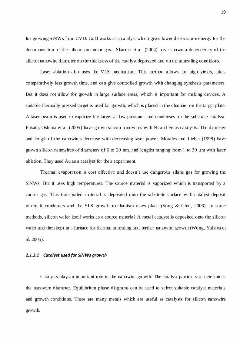
Figure 2.3: Phase diagram of Au-Si Eutectic alloy, which forms at 363oC. At the eutectic temperature, the alloy has
19.5% of Si atoms. (Wong, Yahaya et al. 2005).
Gold is a well-known catalyst which is used for silicon nanowire growth. The eutectic
temperature for Au/Si is 363oC which allows low temperature growth for silicon nanowires (Figure
2.3). The silicon solubility in Au-Si alloy at the eutectic temperature is high which makes the growth
process robust against fluctuations of the silicon concentration. To understanding this statement, let us
consider a half-spherical Au-Si catalyst particle with a diameter of 10 nm. It has approximately
1.5*104 Au atoms and 2.5*103 Si atoms at the eutectic temperature. If there is a change of plus/minus
one silicon atom then the relative concentration of silicon will change by only 0.04%. Now suppose
the silicon concentration is very small at the eutectic temperature (e.g. In-Si alloy), then a fluctuation
of plus or minus one silicon atom will give very high relative concentration change, and will affect the
stability of the growth process. High silicon solubility in Au-Si alloy will support the stable growth
process. Gold has a low vapour pressure at moderate temperatures which reduces the chance of the re-
evaporation of the catalyst material during the growth process.
21
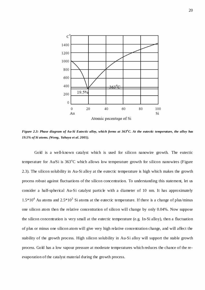
Figure 2.4: Binary Phase diagram of Ni-Si alloy (Lu and et al. 2006).
Wong, Yahaya et al. (2005) have shown the successful growth of silicon nanowires via solid-
liquid-solid mechanism using gold as a catalyst. Nickel has the possibility to act as a catalyst for
silicon nanowire growth. Yan, Xing et al. (2000) and Hsu and Huang (2006) have used nickel as a
catalyst for silicon nanowire growth. Yan, Xing et al. (2000) have grown amorphous silicon nanowires
with an average diameter 20 nm using a Ni layer of 40nm as a catalyst. Hsu and Huang (2006) have
synthesized silicon nanowires using electroplating technique of nickel catalyst on silicon substrates.
They have shown that the diameters, lengths and the growth densities could be controlled by the nickel
content of the deposited layer on the silicon substrate. Figure 2.4 presents the phase diagram of the
nickel and silicon. During the growth process nickel makes nickel silicide whose eutectic temperature
is 966oC with 57% of silicon concentration.
Titanium has a eutectic temperature at 1330oC and has shown the suitability as a catalyst for
silicon nanowire growth (Sharma, Kamins et al. 2004). Aluminium is also a potential candidate as a
catalyst for silicon nanowire growth. The eutectic temperature for Al-Si alloy is 577oC with 12% of
silicon concentration which is less comparable to gold (eutectic temperature 363oC with 19.5% of Si

22
concentration), but greater than other metals. Iron also has proved suitable for the growth of silicon
nanowires but it needs high temperature (around 1200oC).
We have chosen Ni and Au as a catalyst in this research due to their proven ability to grow
SiNWs. Au has been chosen due to higher silicon solubility in the Au-Si alloy at eutectic temperature
and also due to low eutectic temperature. Ni has been chosen due to high Ni concentration in nickel
silicide at the eutectic temperature.
2.2 Carbon Nanotubes
In the past two decades, researchers have been working extensively in the field of carbon
nanoscience. Crystalline carbon exists mainly in four states:
1. Graphite
2. Diamond
3. Fullerenes
4. Carbon Nanotubes
Carbon nanotubes were first identified by Japanese scientist Pro f. Iijima in 1991 as one-
dimensional structures. Carbon nanotubes are hollow cylinders which are made from graphene sheets,
which are capped by pentagonal carbon rings. sp2 hybridized carbon atoms are arranged in mono-
atomic layers of graphene. If there are several coaxial sheets comprising nanotubes, then they are
called multi-wall carbon nanotubes (MWNTs), while if there is only one layer then it is single- wall
carbon nanotubes (SWNTs).
Graphene has an sp2 hybridized structure, in which each carbon atom fill the planar sp2 hybrid
orbit and form 3 in-plane ζ-bonds and one out of plane π-bond, which is perpendicular to the ζ-bond
surface. This makes a planar hexagonal network. These networks are held together by Van der Waals
forces in graphite and the spacing between these sheets is 0.345nm. Due to its circular curvature, these
sp2 bonds rehybridize and these 3 ζ bonds are slightly out of the plane and the π-bond becomes more
23
delocalized outside the plane for compensation with ζ-bonds. This structure makes carbon nanotubes
more mechanically strong and electrically conductive than graphite. Due to this structure, sometimes
they allow some defects in that hexagonal structure, like pentagons and heptagons, which forms bent
and helical nanotubes. (Baughman, Zakhidov et al. 2002)
Figure 2.5: Schematic presentation of the way to form carbon nanotubes from a grapheme sheet (Baughman, Zakhidov
et al. 2002)
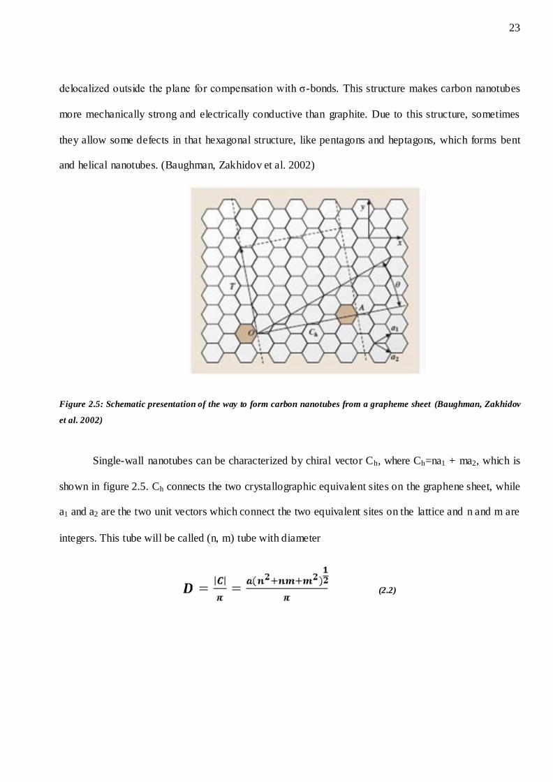
Single-wall nanotubes can be characterized by chiral vector Ch, where Ch=na1 + ma2, which is
shown in figure 2.5. Ch connects the two crystallographic equivalent sites on the graphene sheet, while
a1 and a2 are the two unit vectors which connect the two equivalent sites on the lattice and n and m are
integers. This tube will be called (n, m) tube with diameter
(2.2)
24
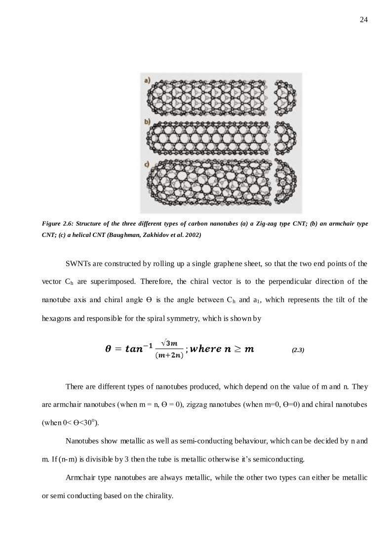
Figure 2.6: Structure of the three different types of carbon nanotubes (a) a Zig-zag type CNT; (b) an armchair type
CNT; (c) a helical CNT (Baughman, Zakhidov et al. 2002)
SWNTs are constructed by rolling up a single graphene sheet, so that the two end points of the
vector Ch are superimposed. Therefore, the chiral vector is to the perpendicular direction of the
nanotube axis and chiral angle Ө is the angle between Ch and a1, which represents the tilt of the
hexagons and responsible for the spiral symmetry, which is shown by
(2.3)
There are different types of nanotubes produced, which depend on the value of m and n. They
are armchair nanotubes (when m = n, Ө = 0), zigzag nanotubes (when m=0, Ө=0) and chiral nanotubes
(when 0< Ө<30o).
Nanotubes show metallic as well as semi-conducting behaviour, which can be decided by n and
m. If (n-m) is divisible by 3 then the tube is metallic otherwise it‘s semiconducting.
Armchair type nanotubes are always metallic, while the other two types can either be metallic
or semi conducting based on the chirality.
25
2.2.1 Physical Properties of CNTs
Due to their structure, MWNTs are mechanically strong and more electrically conductive than
graphite. The diameter of SWNTs has an inverse relationship with their bandgap. This is the key factor
to control the bandgap of the nanotubes. Carbon nanotubes show many properties due to their
nanometer size, which can be employed in many applications. CNTs have exceptional mechanical
strength; they have a very high Young modulus in their axial direction (0.64 TPa for (10, 10) SWNT),
high tensile strength (~37 GPa for (8, 9) SWNT), and extraordinary flexibility (Hofmann, Ducati et al.
2003). They have proposed uses including hydrogen storage devices, field emission devices, as
nanoprobe tips, nanoscale electronic devices, and electrochemical devices (Baughman, Zakhidov et al.
2002).
The electronic properties of CNTs are dependent on their geometry and structure. The bandgap
of large gap nanotubes decrease in proportion to 1/r, while the band gap of small gap nanotubes
decrease with 1/r2; where r is the radius of the nanotubes. Experimentally, the lowest diameter of CNT
produced is 3.5 Å (Kim, Shi et al. 2001).
CNTs have very good transport properties. They are one dimensional nanostructures, so
currents can be transported for long lengths in one direction without any heating effects. Phonons can
also be transport very easily. The thermal conductance for MWNT is ~3000 W/m.K, which is greater
than that of graphite (2000 W/m.K) (Salvetat, Bonard et al. 1999).
2.2.2 Applications of CNTs
The application of specific CNTs depend on their size and orientation. For example, large
diameter CNTs can be used in energy devices such as in fuel cells, lithium ion secondary batteries, and
hydrogen storage (Jang, Lee et al. 2005). Current hydrogen storage methods involve pressurized,
cryogenic vessels, or the use of chemical compounds which release hydrogen upon heating. Carbon
26
nanotubes are attracting interest as hydrogen storage media, as, in principle, hydrogen gas can be
stored within their core (Collins, Arnold et al. 2001).
CNTs have been shown to exhibit electrical conductivity by means of electrons traveling
ballistically inside their cores. These electrons move inside the carbon nanotubes without losing
energy. This renders CNTs potentially useful in electronics, e.g., transistors, field emitting devices.
Bandaru, Daraio et al. (2005) have shown Y-shaped carbon nanotubes behave as electronic
switches similar to conventional MOS transistors. These transistors exhibit better electronic properties
compared to conventional transistors. CNT transistors can operate at extremely fast microwave
frequencies which open the potential for much faster devices with reduced power consumption. Li, Yu
et al. (2004) have reported single SWNT transistor operation at microwave frequencies.
CNTs can also be used as nanoprobes and sensors due to their flexibility and conductive
properties (Nakayama and Akita 2003). Li, Lu et al. (2003) have fabricated a sensor by using SWNTs
for gas and organic vapour detection at room temperature. These SWCNT based sensors can detect gas
levels at low concentrations (ppm) at room temperature, whilst conventional metal oxide microfilm
sensors require an operating temperature >350oC. SWNTs experience a change in conductivity as a
result of gas molecules adsorbing at defect sites. Gases such as NO2 and nitro-toluene have been tested
successfully for this purpose. Someya, Small et al. (2003) have fabricated alcohol vapour sensors
based on SWNT-FETs. When SWNT-FETs are exposed to various kinds of alcohol vapours they
exhibit a significant change in their drain current. They suggest that the sensing mechanism of the
nanotubes FET might be related to electrochemical adsorption or reaction of alcoholic vapo urs. The
adsorption or reaction of the alcoholic molecule could dope the nanotube or it could change the
substrate potential by electrochemical adsorption to the silicon oxide surface, filling out the charge
traps. It could also alter the Schottky barrier at the nanotube-metal interface indirectly by changing the
doping level and/or incomplete screening of electrostatics.
CNTs have also been used to reinforce ceramic and composite materials due to their high
mechanical tensile strength, good flexibility and low weight (Yamamoto and et al. 2008).
27
2.2.3 Carbon Nanotube Growth
There are many methods to grow CNTs: e.g. arc-discharge (Ando and Zhao 2006; Kim and
Kim 2007), laser ablation (Kuo, Chi et al. 2001; Vander Wal, Berger et al. 2003) and CVD (Brukh and
Mitra 2006; Hart and et al. 2006). Early workers used the arc discharge method with metal catalyst as
shown by S. Iijima et al. in 1991. Here, the nanotubes were produced by arc vaporization generated by
applying a high electric current between two graphite electrodes, separated by approximately 1 mm, in
an inert atmosphere. This method yields carbon nanotubes in very large quantities, but it requires
extremely high operating temperatures, around 4000°C.
Pulsed Laser Ablation is a fast method, which employs a graphite target as a carbon source.
Ablation of the graphite target at low pressure gives carbon nanotubes growth in plasma condensation.
Chemical Vapour Deposition (CVD) growth is a large-area compatible process, where the
CNTs grow uniformly over the surface of the substrate. Growth of nanotubes is controlled by the
choice of catalyst, the gas sources and substrates and temperature. Nanotubes are grown from
nucleation sites of a catalyst material on the surface. (Brukh & Mitra, 2006)
2.2.3.1 Catalysts used for CNT growth
Carbon nanotubes produced from catalytic CVD allow for large area synthesis (Rana, Koltypin
et al. 2001). The composition of the bimetallic catalysts significantly affects the carbon nanotube
growth (Liao, Serquis et al. 2003; Pint and et al. 2008). Let us take an example of carbon nanotube
growth with Co-Mo as a catalyst. A high concentration of Mo in Co-Mo is effective in producing
single-wall carbon nanotubes. When there is only Co as a catalyst then it produces multiwall carbon
nanotubes whilst alone Mo is inactive at 700oC and produces single-wall carbon nanotubes at 1200oC.
Rümmeli, Kramberger et al. (2007) have shown that the grown carbon nanotubes depend on the
volume to surface area ratio of the catalyst particle. Ohara, Neo et al. (2008) have grown multiwall
carbon nanotubes using iron as a catalyst. Wongwiriyapan, Katayama et al. (2008) have grown single
28
walled carbon nanotubes with Fe/Al and Fe catalysts. Fe/Al catalyst gives uniform diameters of carbon
nanotubes while Fe catalyst gives scattered diameters of carbon nanotubes. Al layers act as a support
material which promotes the formation of the catalyst nano-particles with a high number density and
uniform sizes. Abdi, Arzi et al. (2008) have grown carbon nanotubes by PECVD using Ni as a catalyst
with acetylene and hydrogen as a gas mixture at 650oC. Transition metal catalysts such as Fe and Co
have strong catalytic activities for both the decomposition of hydrocarbon feedstock and the formation
of graphite carbons. Yoshihara, Ago et. al. (2008) have grown carbon nanotubes by CVD in the
presence of Au nanoclusters. Carbon has low solubility in gold. They have observed catalytic activity
of gold supported on various metal oxides, alumina, silica, titania and magnesia with different
hydrocarbon feedstocks, methane (CH4), ethylene (C2H4) and acetylene (C2H2). They recorded a very
limited catalytic effect of gold for the decomposition for hydrocarbon feedstock (Yoshihara, Ago et al.
2008). Liu, Chokan et al. (2008) have grown single walled carbon nanotubes (SWCNTs) using gold as
a catalyst.
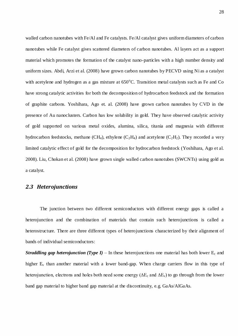
2.3 Heterojunctions
The junction between two different semiconductors with different energy gaps is called a
heterojunction and the combination of materials that contain such heterojunctions is called a
heterostructure. There are three different types of heterojunctions characterized by their alignment of
bands of individual semiconductors:
Straddling gap heterojunction (Type I) – In these heterojunctions one material has both lower Ec and
higher Ev than another material with a lower band-gap. When charge carriers flow in this type of
heterojunction, electrons and holes both need some energy (∆Ec and ∆Ev) to go through from the lower
band gap material to higher band gap material at the discontinuity, e.g. GaAs/AlGaAs.
29
Staggered gap heterojunction (Type II) – One material has both lower Ec and lower Ev than the other
material with the low band-gap. When charge flows in this heterojunction then one type of carrier
needs energy while second carrier gains energy, e.g InP/InSb
Broken gap heterojunctrion (Type III) – These heterojunctions are similar to Type II heterojunctions
but the Ec of material is lower than Ev of another material. The band-gap doesn‘t overlap. Case is
similar to the Type II heterojunction but the difference between the Fermi levels is high, e.g.
GaSb/InAs.
Due to the alignment of the bands, the energy of the conduction and valence bands change. The
magnitude of the change in energy is important in device fabrication of heterojunctions.
Figure 2.7: Straddling gap (Type I), Staggering gap (Type II) and Broken gap (Type III) heterojunctions. Ec Lowest
conduction band energy, Ev Highest valance band energy, EF Fermi energy, qχ is electron affinity (the work needed to
remove a charge from the lowest conduction band edge to the infinity), q φ is the Work function (energy needed to
remove the energy from the Fermi level to the infinity) (Foll 2011).
2.3.1 Band Diagram of the Heterojunction
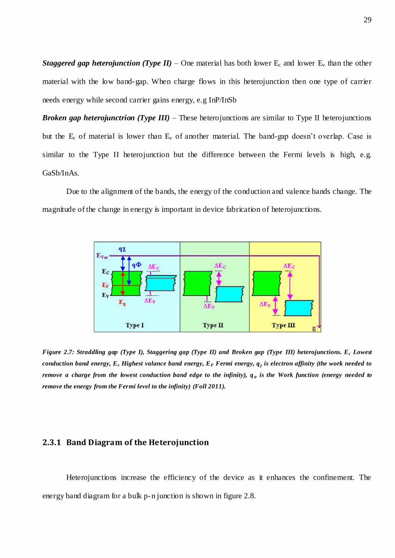
Heterojunctions increase the efficiency of the device as it enhances the confinement. The
energy band diagram for a bulk p-n junction is shown in figure 2.8.
30
Figure 2.8: P-n junction under (a) zero bias and (b) forward bias condition. Under forward bias conditions, minority
carriers diffuse into the neutral regions (Schubert 2011).
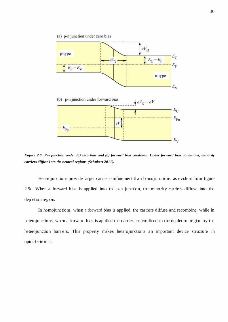
Heterojunctions provide larger carrier confinement than homojunctions, as evident from figure
2.9c. When a forward bias is applied into the p-n junction, the minority carriers diffuse into the
depletion region.
In homojunctions, when a forward bias is applied, the carriers diffuse and recombine, while in
heterojunctions, when a forward bias is applied the carrier are confined to the depletion region by the
heterojunction barriers. This property makes heterojunctions an important device structure in
optoelectronics.
31
(a) Homojunction under zero bias
(b) Homojunction under forward bias
(c) Heterojunction under forward bias
Figure 2.9: Band diagram of a p-n junction. P-n homojunction under (a) zero and (b) forward bias. p-n heterojunction
under forward bias. In homojunctions, carriers diffuse, on average, over the diffusion lengths L n and Lp before
recombining. In heterojunctions, carriers are confined by the heterojunctions barriers (Schubert 2011).
32
2.3.2 Metal/Semiconductor (MS) Junctions
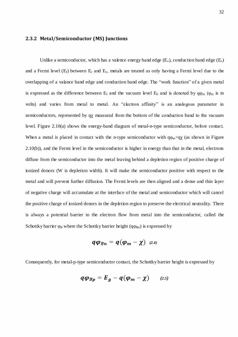
Unlike a semiconductor, which has a valence energy band edge (Ev), conduction band edge (Ec)
and a Fermi level (Ef) between Ec and Ev, metals are treated as only having a Fermi level due to the
overlapping of a valance band edge and conduction band edge. The ―work function‖ of a given metal
is expressed as the difference between Ef and the vacuum level E0 and is denoted by qφm (φm is in
volts) and varies from metal to metal. An ―electron affinity‖ is an analogous parameter in
semiconductors, represented by qχ measured from the bottom of the conduction band to the vacuum
level. Figure 2.10(a) shows the energy-band diagram of metal-n-type semiconductor, before contact.
When a metal is placed in contact with the n-type semiconductor with qφm>qχ (as shown in Figure
2.10(b)), and the Fermi level in the semiconductor is higher in energy than that in the metal, electrons
diffuse from the semiconductor into the metal leaving behind a depletion region of positive charge of
ionized donors (W is depletion width). It will make the semiconductor positive with respect to the
metal and will prevent further diffusion. The Fermi levels are then aligned and a dense and thin layer
of negative charge will accumulate at the interface of the metal and semiconductor which will cancel
the positive charge of ionized donors in the depletion region to preserve the electrical neutrality. There
is always a potential barrier to the electron flow from metal into the semiconductor, called the
Schottky barrier φB where the Schottky barrier height (qφBn) is expressed by
(2.4)
Consequently, for metal-p-type semiconductor contact, the Schottky barrier height is expressed by
(2.5)
33
where Eg is the semiconductor band gap. Figure 2.10 (c and d) presents the energy-band diagram of a
metal-n-type semiconductor contact under forward and reverse bias conditions. VF is the applied
forward bias and VR is the applied reverse bias.
Figure 2.10: Energy-band diagram for metal-n-type semiconductor contact under different biasing conditions. (a)
before contact; (b) after contact at equilibrium; (c) at forward bias; and (d) at reverse bias.
However, the barrier height depends on other factors too. There is a weak dependency
attributed to interface states with energies within the band gap of the semiconductor that are present in
close vicinity of the metal. This dependency, together with any space charge in the dep letion layer, is
balanced by an equal amount of opposite charge on the metal surface. This results in dipole behaviour
over a distance δ of atomic dimensions. The potential drop over this dipole modifies the Schottky
barrier height.
34
In M-S junctions the current is mainly due to majority charge carriers. For an n-type
semiconductor, majority carrier electrons flow from the semiconductor into the metal and leaves
behind a positive charge due to the ionized donor atoms. A negative field is created due to this positive
charge at the interface which in turn lowers the band edges of the semiconductors. The diffusion of
electrons from the metal into the n-type semiconductor is prevented due to the large Schottky barrier
ΦBn at the junction for electrons. At thermal equilibrium, the resultant current should be zero. This
causes an accumulation of charge at the interface, which creates a depletion region or space charge
region. In metals this is negative charge and in the semiconductor it is a positive charge. This creates
bending in the band at the interface, which behaves as a barrier for the charge carriers. This barrier is
called a Schottky barrier. The potential across the semiconductor is called a built- in-potential. In either
bias condition, the majority carrier current is always significantly greater than the minority current.
Under forward bias conditions, when the metal is held at the neutral potential while the n-type
semiconductor is at a negative potential, the Fermi energy of the semiconductor is at a higher energy
level compared to the Fermi energy of the metal, which enhances the electron drift current from the
semiconductor into the metal. This gives a positive current at the junction with a voltage equal to the
built- in potential.
Under reverse bias conditions, when the metal is held at the neutral potential while the n-type
semiconductor is held at a positive potential, the Fermi energy of n-type semiconductor is at a lower
level than the Fermi energy of the metal, which increases the built- in potential across the
semiconductor. It increases the barrier height, which ceases the flow of electron diffusion current from
the semiconductor into the metal. So there would not be any resultant current in the reverse bias
condition. This is the rectifying behavior of the Schottky diodes, which gives current in forward bias
due to majority charge carriers, while it does not give any current in the reverse bias junction.
A tentative band diagram of the CNT-n-type SiNW heterojunction has been made on the basis
of the work function and band gaps of the carbon nanotubes and silicon nanowires using the Anderson
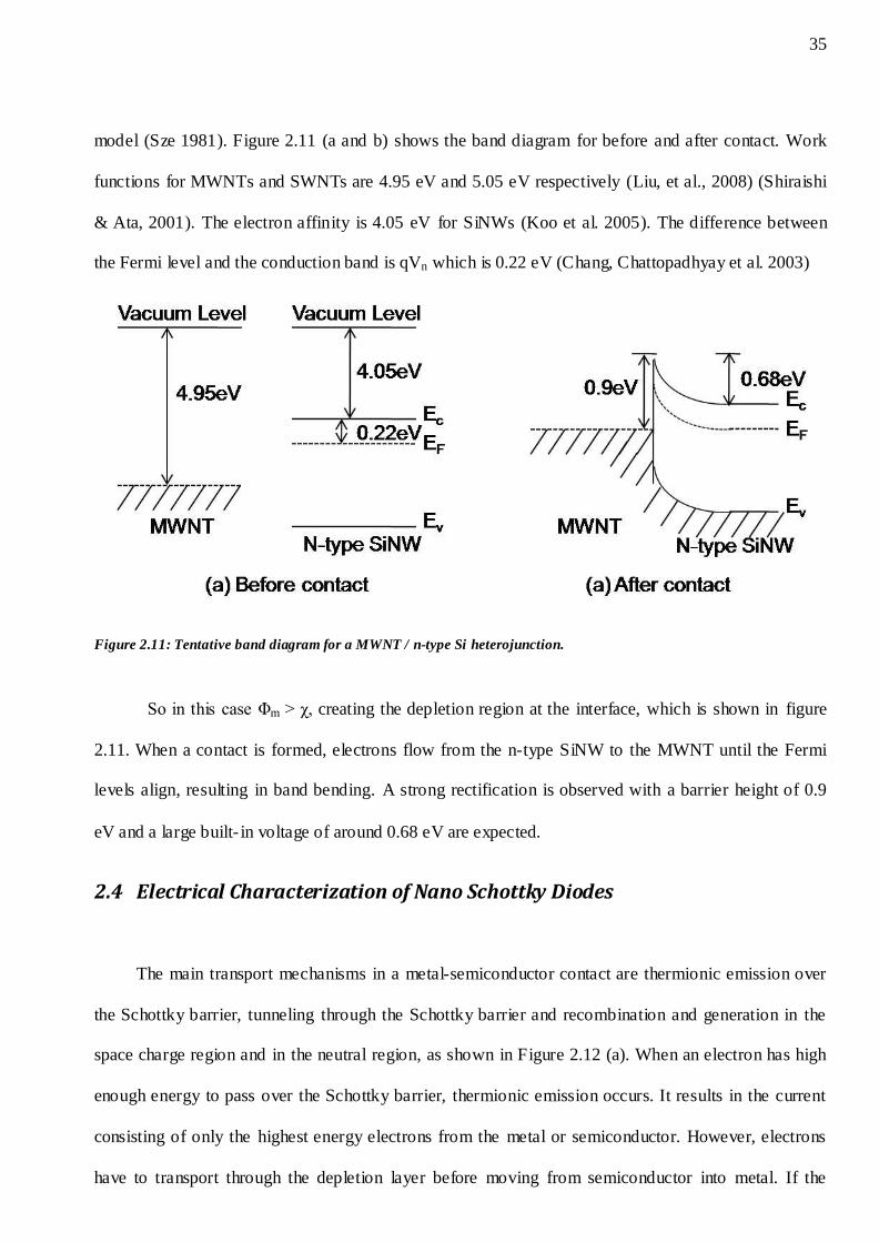
35
model (Sze 1981). Figure 2.11 (a and b) shows the band diagram for before and after contact. Work
functions for MWNTs and SWNTs are 4.95 eV and 5.05 eV respectively (Liu, et al., 2008) (Shiraishi
& Ata, 2001). The electron affinity is 4.05 eV for SiNWs (Koo et al. 2005). The difference between
the Fermi level and the conduction band is qVn which is 0.22 eV (Chang, Chattopadhyay et al. 2003)
Figure 2.11: Tentative band diagram for a MWNT / n-type Si heterojunction.
So in this case Φm > χ, creating the depletion region at the interface, which is shown in figure
2.11. When a contact is formed, electrons flow from the n-type SiNW to the MWNT until the Fermi
levels align, resulting in band bending. A strong rectification is observed with a barrier height of 0.9
eV and a large built- in voltage of around 0.68 eV are expected.
2.4 Electrical Characterization of Nano Schottky Diodes
The main transport mechanisms in a metal-semiconductor contact are thermionic emission over
the Schottky barrier, tunneling through the Schottky barrier and recombination and generation in the
space charge region and in the neutral region, as shown in Figure 2.12 (a). When an electron has high
enough energy to pass over the Schottky barrier, thermionic emission occurs. It results in the current
consisting of only the highest energy electrons from the metal or semiconductor. However, electrons
have to transport through the depletion layer before moving from semiconductor into metal. If the
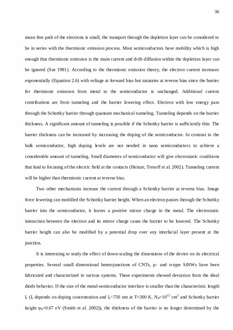
36
mean free path of the electrons is small, the transport through the depletion layer can be considered to
be in series with the thermionic emission process. Most semiconductors have mobility which is high
enough that thermionic emission is the main current and drift-diffusion within the depletion layer can
be ignored (Sze 1981). According to the thermionic emission theory, the electron current increases
exponentially (Equation 2.6) with voltage at forward bias but saturates at reverse bias since the barrier
for thermionic emission from metal to the semiconductor is unchanged. Additional current
contributions are from tunneling and the barrier lowering effect. Electron with low energy pass
through the Schottky barrier through quantum mechanical tunneling. Tunneling depends on the barrier
thickness. A significant amount of tunneling is possible if the Schottky barrier is sufficiently thin. The
barrier thickness can be increased by increasing the doping of the semiconductor. In contrast to the
bulk semiconductor, high doping levels are not needed in nano semiconductors to achieve a
considerable amount of tunneling. Small diameters of semiconductor will give electrostatic conditions
that lead to focusing of the electric field at the contacts (Heinze, Tersoff et al. 2002). Tunneling current
will be higher than thermionic current at reverse bias.
Two other mechanisms increase the current through a Schottky barrier at reverse bias. Image
force lowering can modified the Schottky barrier height. When an electron passes through the Schottky
barrier into the semiconductor, it leaves a positive mirror charge in the metal. The electrostatic
interaction between the electron and its mirror charge cause the barrier to be lowered. The Schottky
barrier height can also be modified by a potential drop over any interfacial layer present at the
junction.
It is interesting to study the effect of down-scaling the dimensions of the device on its electrical
properties. Several small dimensional heterojunctions of CNTs, p- and n-type SiNWs have been
fabricated and characterized in various systems. These experiments showed deviation from the ideal
diode behavior. If the size of the metal-semiconductor interface is smaller than the characteristic length
lc (lc depends on doping concentration and lc~750 nm at T=300 K, Nd=1015 cm3 and Schottky barrier
height φb=0.67 eV (Smith et al. 2002)), the thickness of the barrier is no longer determined by the
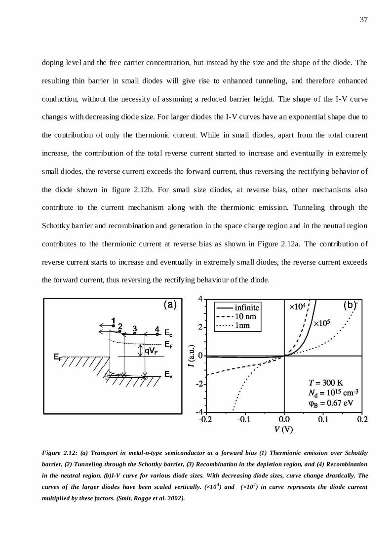
37
doping level and the free carrier concentration, but instead by the size and the shape of the diode. The
resulting thin barrier in small diodes will give rise to enhanced tunneling, and therefore enhanced
conduction, without the necessity of assuming a reduced barrier height. The shape of the I-V curve
changes with decreasing diode size. For larger diodes the I-V curves have an exponential shape due to
the contribution of only the thermionic current. While in small diodes, apart from the total current
increase, the contribution of the total reverse current started to increase and eventually in extremely
small diodes, the reverse current exceeds the forward current, thus reversing the rect ifying behavior of
the diode shown in figure 2.12b. For small size diodes, at reverse bias, other mechanisms also
contribute to the current mechanism along with the thermionic emission. Tunneling through the
Schottky barrier and recombination and generation in the space charge region and in the neutral region
contributes to the thermionic current at reverse bias as shown in Figure 2.12a. The contribution of
reverse current starts to increase and eventually in extremely small diodes, the reverse current exceeds
the forward current, thus reversing the rectifying behaviour of the diode.
Figure 2.12: (a) Transport in metal-n-type semiconductor at a forward bias (1) Thermionic emission over Schottky
barrier, (2) Tunneling through the Schottky barrier, (3) Recombination in the depletion region, and (4) Recombination
in the neutral region. (b)I-V curve for various diode sizes. With decreasing diode sizes, curve change drastically. The
curves of the larger diodes have been scaled vertically. (×104) and (×10
4) in curve represents the diode current
multiplied by these factors. (Smit, Rogge et al. 2002).
38
Non-linear I-V characteristics of nano Schottky diodes are mainly due to the Schottky barrier and
depend strongly on the barrier height. Depending on the Schottky barrier height, at least four types of
I-V characteristics have been observed:
1. Linear I-V characteristics (Wang et al. 2003) (Cui et al. 2000) (Zhang et al. 2003).
2. Symmetric I-V characteristics
3. Asymmetric I-V characteristics (Wang et al. 2003) (Cui et al. 2000) (Zhang et al. 2006) (Chung
et al. 2000) (Heo et al. 2004)
4. Rectifying I-V characteristics (Fan & Lu 2005) (Lee et al. 2005)
2.4.1 Thermionic Field Emission Theory
Thermionic emission theory is the most successful and widely used theory for modeling planar
Schottky junctions. The main component of tunneling current is missing from the thermionic emission
theory which becomes the dominating component under reverse bias and especially for low dimension
systems (Appenzeller et al. 2004; Gu et al. 2005; Yu et al. 1998). This current must be included in the
general emission theory.
We will analyze our Schottky diodes on the basis of the thermionic field emission model of
Padovani and Stratton (1966). Let us start with Schottky diode of metal-n-type semiconductor. In an n-
type semiconductor, electron currents dominate the I-V characteristics and for large band gap
materials, we may ignore the hole current. For nano M-S junctions, where the forward current itself is
of the order of nA, then we cannot ignore the reverse bias current. Tunneling through the reverse bias
Schottky barrier becomes significant. When a moderately large reverse bias is applied to the Schottky
junction then it can cause the potential barrier to become thin enough for significant tunneling of
electrons from metal to semiconductor (Rhoderick & Williams, 1988). According to the thermionic
emission theory the current density equation of a Schottky junction is given by (Rhoderick &
Williams, 1988)
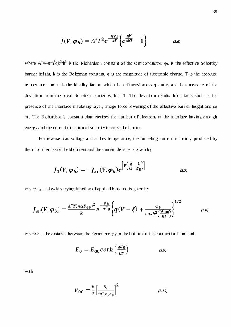
39
(2.6)
where A*=4πm*qk2/h3 is the Richardson constant of the semiconductor, φb is the effective Schottky
barrier height, k is the Boltzman constant, q is the magnitude of electronic charge, T is the absolute
temperature and n is the ideality factor, which is a dimensionless quantity and is a measure of the
deviation from the ideal Schottky barrier with n=1. The deviation results from facts such as the
presence of the interface insulating layer, image force lowering of the effective barrier height and so
on. The Richardson‘s constant characterizes the number of electrons at the interface having enough
energy and the correct direction of velocity to cross the barrier.
For reverse bias voltage and at low temperature, the tunneling current is mainly produced by
thermionic emission field current and the current density is given by
(2.7)
where Jsr is slowly varying function of applied bias and is given by
(2.8)
where ξ is the distance between the Fermi energy to the bottom of the conduction band and
(2.9)
with
(2.10)
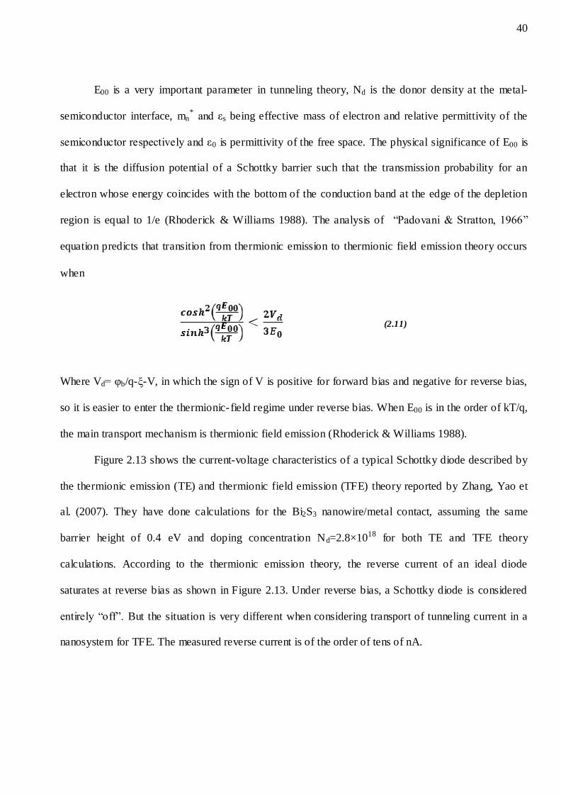
40
E00 is a very important parameter in tunneling theory, Nd is the donor density at the metal-
semiconductor interface, mn* and εs being effective mass of electron and relative permittivity of the
semiconductor respectively and ε0 is permittivity of the free space. The physical significance of E00 is
that it is the diffusion potential of a Schottky barrier such that the transmission probability for an
electron whose energy coincides with the bottom of the conduction band at the edge of the depletion
region is equal to 1/e (Rhoderick & Williams 1988). The analysis of ―Padovani & Stratton, 1966‖
equation predicts that transition from thermionic emission to thermionic field emission theory occurs
when
(2.11)
Where Vd= φb/q-ξ-V, in which the sign of V is positive for forward bias and negative for reverse bias,
so it is easier to enter the thermionic-field regime under reverse bias. When E00 is in the order of kT/q,
the main transport mechanism is thermionic field emission (Rhoderick & Williams 1988).
Figure 2.13 shows the current-voltage characteristics of a typical Schottky diode described by
the thermionic emission (TE) and thermionic field emission (TFE) theory reported by Zhang, Yao et
al. (2007). They have done calculations for the Bi2S3 nanowire/metal contact, assuming the same
barrier height of 0.4 eV and doping concentration Nd=2.8×10¹⁸ for both TE and TFE theory
calculations. According to the thermionic emission theory, the reverse current of an ideal diode
saturates at reverse bias as shown in Figure 2.13. Under reverse bias, a Schottky diode is considered
entirely ―off‖. But the situation is very different when considering transport of tunneling current in a
nanosystem for TFE. The measured reverse current is of the order of tens of nA.
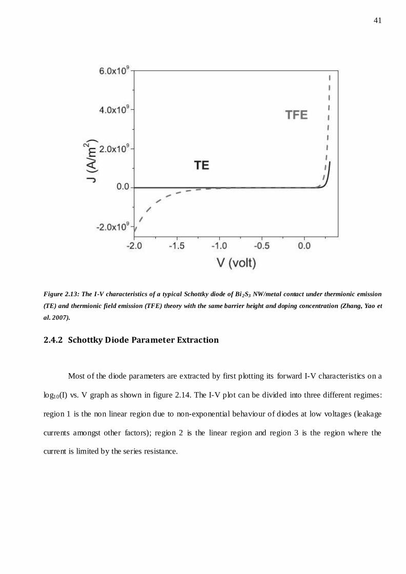
41
Figure 2.13: The I-V characteristics of a typical Schottky diode of Bi2S3 NW/metal contact under thermionic emission
(TE) and thermionic field emission (TFE) theory with the same barrier height and doping concentration (Zhang, Yao et
al. 2007).
2.4.2 Schottky Diode Parameter Extraction
Most of the diode parameters are extracted by first plotting its forward I-V characteristics on a
log10(I) vs. V graph as shown in figure 2.14. The I-V plot can be divided into three different regimes:
region 1 is the non linear region due to non-exponential behaviour of diodes at low voltages (leakage
currents amongst other factors); region 2 is the linear region and region 3 is the region where the
current is limited by the series resistance.
42
Figure 2.14: Semi-logarithmic I-V plot for a typical Schottky or a p-n junction diode (Bashar 1998)
Barrier Height φb: This is defined as the potential barrier to thermionic emission that naturally exists
between an intimate metal and semiconductor contact at zero applied bias. Current by thermionic
emission is assumed and the φb is extracted by fitting a straight line in region 2 of figure 2.14. From
equation 2.6 it is seen that the y-axis intercept of this fit gives the saturation current Is:
(2.12)
Thus
(2.13)

43
This approach requires the modified Richardson constant, A*, to be known for the particular metal-
semiconductor junction (A**=252 A cm-2 K-2 for n-type silicon (Li et al. 2010)).
Ideality Factor (n): Ideality factor (n) is used to quantify the quality of the Schottky diode junction.
For ideal Schottky diode n=1. Slope of Figure 2.14 will give the value of n.
From equation 2.6
(2.14)
Series Resistance (Rs): The series resistance (Rs) is determined from region 3 of figure 2.14 where at
high current, the plot becomes flat and is assumed to be dominated entirely by the Rs. A plot of I-V is
made and Rs is extracted from the point where this curve saturates to a steady minimum value.
Another method to calculate the barrier height, resistance and the ideality factor is Cheung‘s
method. They have shown that these can be calculated using the forward current-voltage (I-V) by
plotting the following two equations
(2.15)
where V is voltage, I is forward diode current, n is ideality factor, k is Boltzmann‘s constant, T is
absolute temperature and R is resistance of the diode. A plot of dV/d(lnI) versus I should be a straight
line with slope Rs and y axis intercept n(kT/q) and
(2.16)
where
(2.17)
44
where Aeff is effective area of the diode, A* (for free electrons A*=120cm-2K-2A (Sze 1981)) is
Richardson constant and øb is the barrier height. A plot of H(I) versus I should be a straight line whose
y axis intercept is nøb and slope will give R.
2.5 Possible growth mechanisms of SiNW/CNT Heterojunction
There may be several methods for synthesizing CNT/SiNW nano Schottky diodes. For
example, CNT/SiNW HJs can be synthesized using the bottom-up method by using a common catalyst
for CNT and SiNW growth. Several mechanisms such as, SLS, VLS, OAG etc have been used to grow
SiNWs and CNTs from bottom-up approaches.
2.5.1 Growth Mechanism for bottom-up growth
There are two main mechanisms for silicon nanowire and carbon nanotube growth: vapour-
liquid-solid (VLS) mechanism and the solid- liquid-solid mechanism (SLS). There are many metal
catalysts such as Ni, Fe which have served as a catalyst for CNT growth as well as SiNW growth. The
use of nickel, iron and gold as the common catalyst is described in the following work. Therefore,
heterojunction can be synthesized by the following two methods:
1. Synthesize silicon nanowires first using metal catalyst, and then further carry on growth for carbon
nanotubes on the top of the nanowires.
2. Grow carbon nanotubes using metal catalyst and then use the same metal for further growth of
SiNWs on the top of the nanotubes.
2.5.1.1 Vapor-Liquid-Solid mechanism
The VLS mechanism was developed by Wagner and Ellis in 1960 (Wagner & Ellis 1964). The
VLS mechanism can be controlled using metal catalysts. There are two types of growth mechanism for
VLS, one is tip growth and second is base growth. The growth is defined by the liquid droplet. The
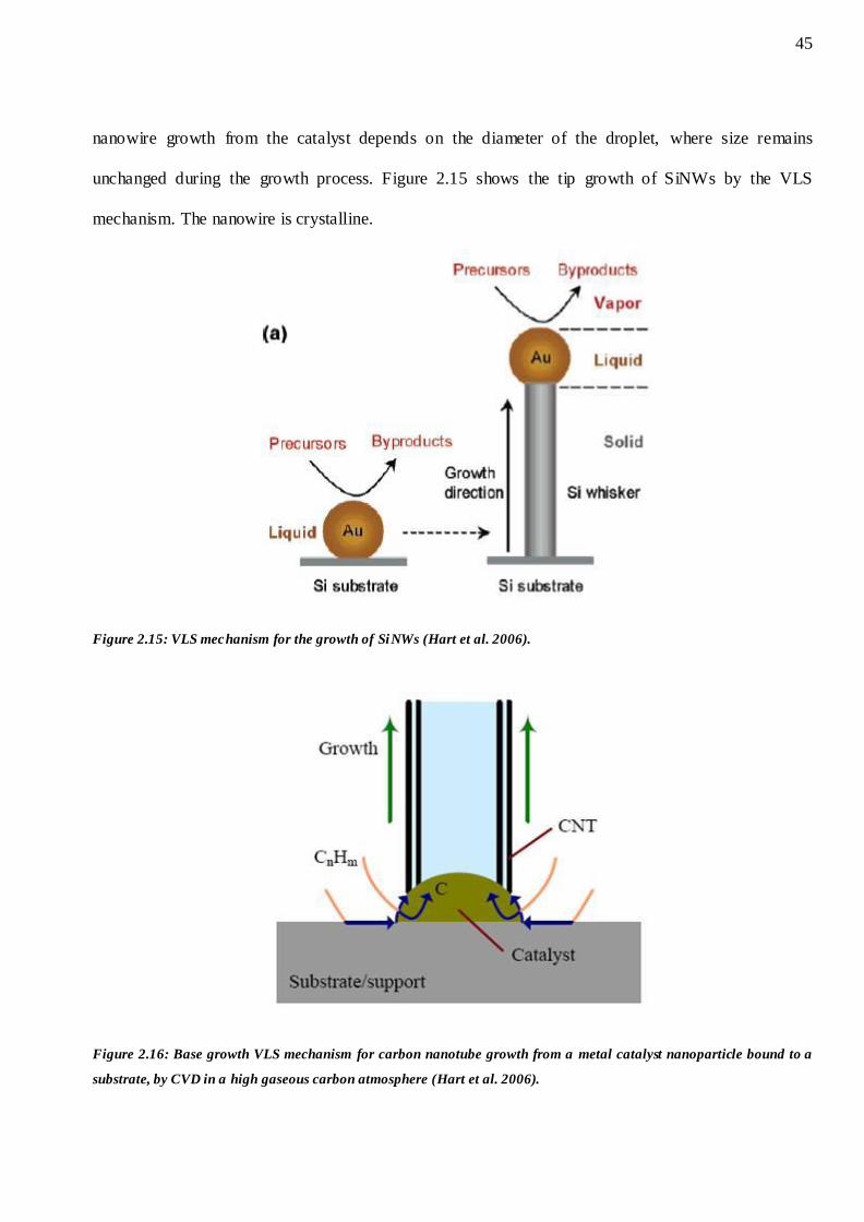
45
nanowire growth from the catalyst depends on the diameter of the droplet, where size remains
unchanged during the growth process. Figure 2.15 shows the tip growth of SiNWs by the VLS
mechanism. The nanowire is crystalline.
Figure 2.15: VLS mechanism for the growth of SiNWs (Hart et al. 2006).
Figure 2.16: Base growth VLS mechanism for carbon nanotube growth from a metal catalyst nanoparticle bound to a
substrate, by CVD in a high gaseous carbon atmosphere (Hart et al. 2006).
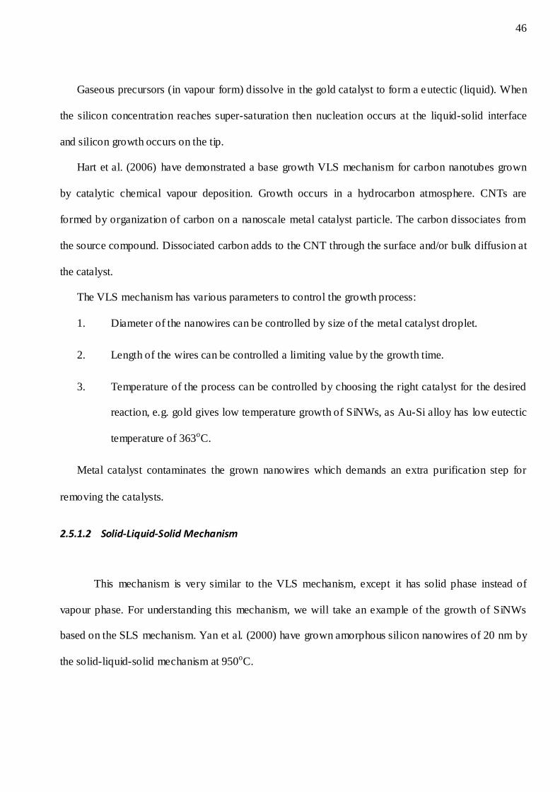
46
Gaseous precursors (in vapour form) dissolve in the gold catalyst to form a eutectic (liquid). When
the silicon concentration reaches super-saturation then nucleation occurs at the liquid-solid interface
and silicon growth occurs on the tip.
Hart et al. (2006) have demonstrated a base growth VLS mechanism for carbon nanotubes grown
by catalytic chemical vapour deposition. Growth occurs in a hydrocarbon atmosphere. CNTs are
formed by organization of carbon on a nanoscale metal catalyst particle. The carbon dissociates from
the source compound. Dissociated carbon adds to the CNT through the surface and/or bulk diffusion at
the catalyst.
The VLS mechanism has various parameters to control the growth process:
1. Diameter of the nanowires can be controlled by size of the metal catalyst droplet.
2. Length of the wires can be controlled a limiting value by the growth time.
3. Temperature of the process can be controlled by choosing the right catalyst for the desired
reaction, e.g. gold gives low temperature growth of SiNWs, as Au-Si alloy has low eutectic
temperature of 363oC.
Metal catalyst contaminates the grown nanowires which demands an extra purification step for
removing the catalysts.
2.5.1.2 Solid-Liquid-Solid Mechanism
This mechanism is very similar to the VLS mechanism, except it has solid phase instead of
vapour phase. For understanding this mechanism, we will take an example of the growth of SiNWs
based on the SLS mechanism. Yan et al. (2000) have grown amorphous silicon nanowires of 20 nm by
the solid-liquid-solid mechanism at 950oC.
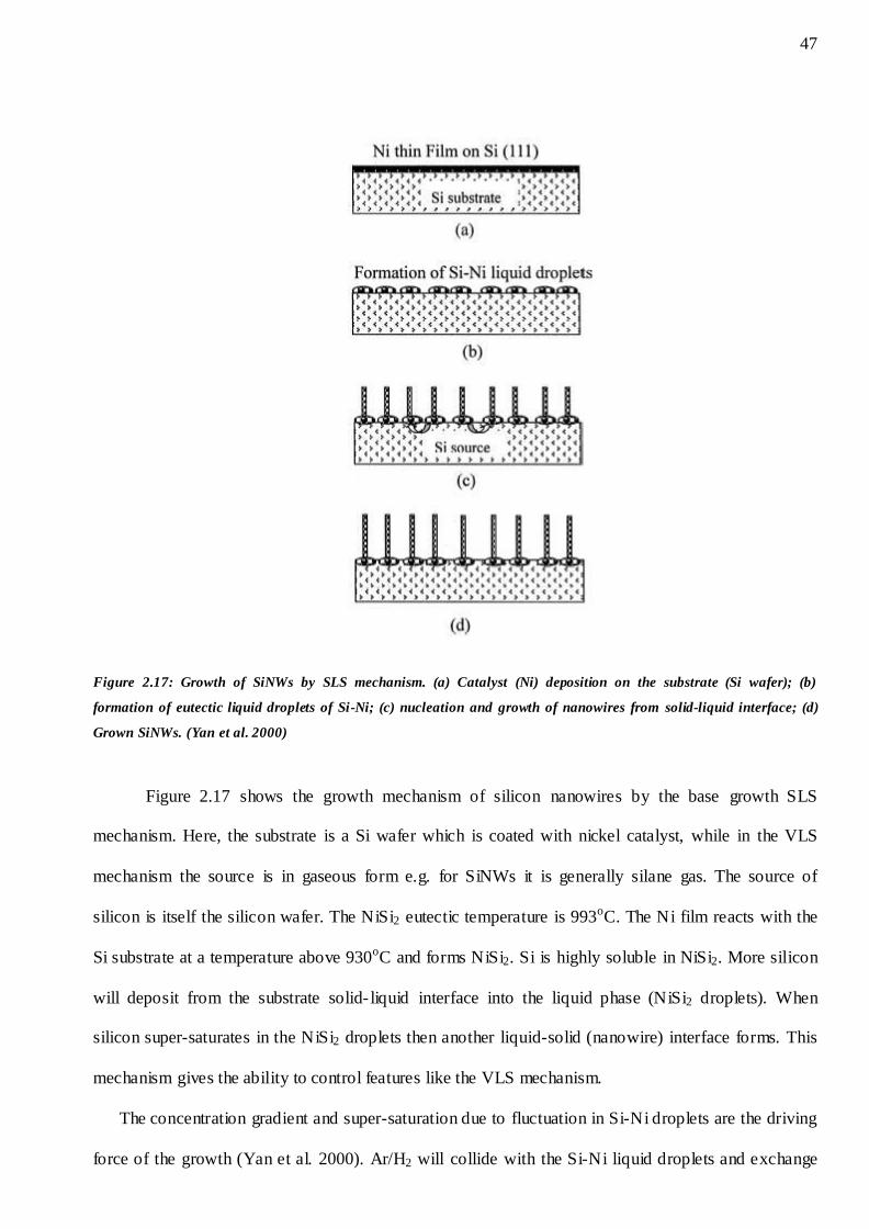
47
Figure 2.17: Growth of SiNWs by SLS mechanism. (a) Catalyst (Ni) deposition on the substrate (Si wafer); (b)
formation of eutectic liquid droplets of Si-Ni; (c) nucleation and growth of nanowires from solid-liquid interface; (d)
Grown SiNWs. (Yan et al. 2000)
Figure 2.17 shows the growth mechanism of silicon nanowires by the base growth SLS
mechanism. Here, the substrate is a Si wafer which is coated with nickel catalyst, while in the VLS
mechanism the source is in gaseous form e.g. for SiNWs it is generally silane gas. The source of
silicon is itself the silicon wafer. The NiSi2 eutectic temperature is 993oC. The Ni film reacts with the
Si substrate at a temperature above 930oC and forms NiSi2. Si is highly soluble in NiSi2. More silicon
will deposit from the substrate solid- liquid interface into the liquid phase (NiSi2 droplets). When
silicon super-saturates in the NiSi2 droplets then another liquid-solid (nanowire) interface forms. This
mechanism gives the ability to control features like the VLS mechanism.
The concentration gradient and super-saturation due to fluctuation in Si-Ni droplets are the driving
force of the growth (Yan et al. 2000). Ar/H2 will collide with the Si-Ni liquid droplets and exchange
48
their energy and momentum with the materials on the surface of the Si-Ni droplets. It causes
overcooling which initiate the preferential unidirectional growth of a-SiNWs.
2.5.2 Mechanisms for SiNW growth from top-down approaches
Several bottom-up techniques have been used to synthesize SiNWs in the literature. SiNWs
growth with a combined mechanism of VLS and SLS has been reviewed in an earlier part of this
chapter. A top-down approach has also shown its importance in silicon nano-pillar formation (Ng, et
al. 2009; Chang et al. 2010). Small separation between nano-pillars can be obtained which is more
difficult through the bottom-up approach where at higher growth temperature, metal catalyst islands
merge and give a challenge to obtain small separation between nano-pillars. Dry etching had been used
earlier by other researchers to fabricate SiNWs through the top-down approach. Dry etching gives
anisotropic etching of the wafer. Prior to etching, a mask is deposited onto the wafer. Top-down
approaches use masking which is followed by etching. Very small features down to <10nm can be
defined by electron-beam lithography followed by etching (Chen & Ahmed, 1993). Though the result
is good the high cost and time consuming process pressurize us to use some different technique for
mask formation to reduce the cost. Natural lithography is one of the options which is explored through
many researches (Hulteen & Duyne, 1995; Peng et al. 2007). Arrays of polystyrene (PS) spheres have
been used for patterning. In this process, PS spheres assembled themselves into close-packed arrays.
Metal islands were formed in between these arrays. Spacing and diameter of these islands can be
controlled by etching of PS spheres or by using different diameter PS spheres. Another low cost and
less time consuming option for nano dots mask formation is nano-particle film made by either spin
coating or dip coating. Similarly self-organized metal islands formation by low temperature annealing
can be a good solution for low cost nano dots mask formation. We have used nano-particles in our
work to make a pattern onto the wafer. Dry etching can be done in an ICP etcher; it gives better results
compared to Reactive Ion Etching (RIE). Details of the ICP system can be found in Chapter 3.
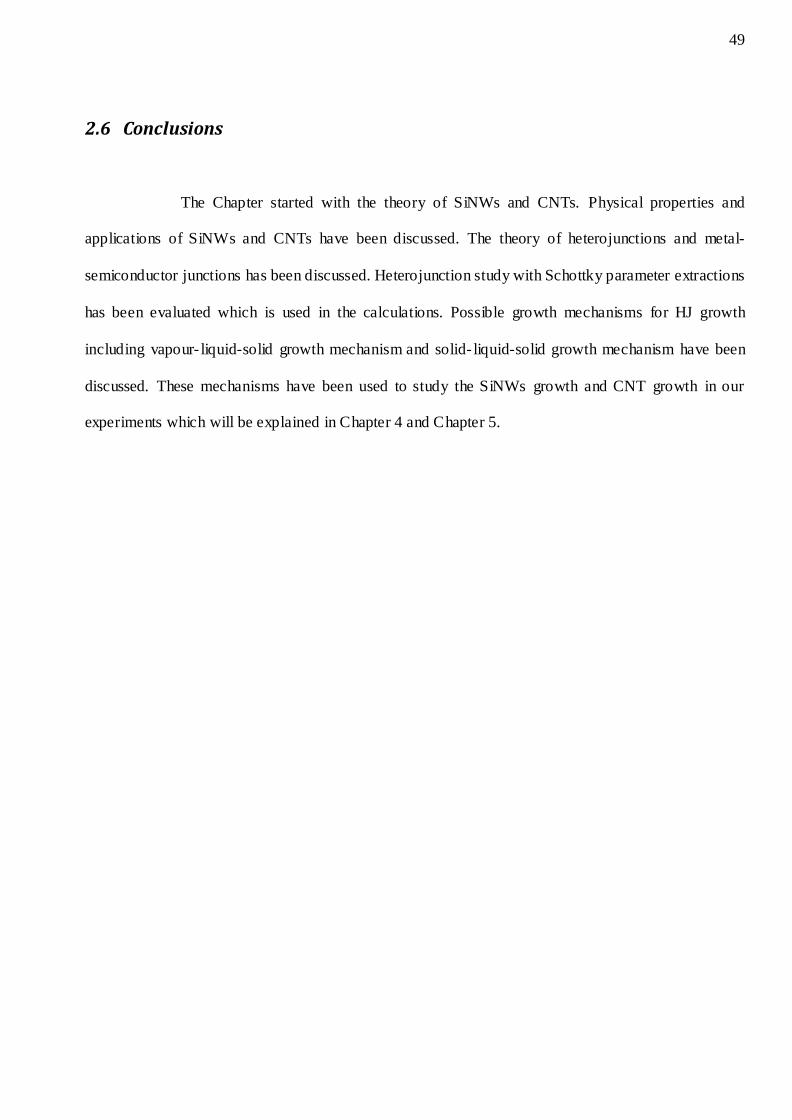
49
2.6 Conclusions
The Chapter started with the theory of SiNWs and CNTs. Physical properties and
applications of SiNWs and CNTs have been discussed. The theory of heterojunctions and metal-
semiconductor junctions has been discussed. Heterojunction study with Schottky parameter extractions
has been evaluated which is used in the calculations. Possible growth mechanisms for HJ growth
including vapour- liquid-solid growth mechanism and solid- liquid-solid growth mechanism have been
discussed. These mechanisms have been used to study the SiNWs growth and CNT growth in our
experiments which will be explained in Chapter 4 and Chapter 5.
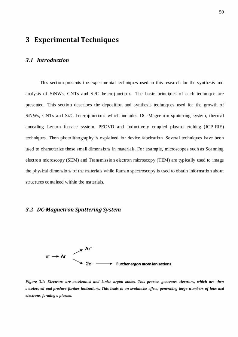
50
3 Experimental Techniques
3.1 Introduction
This section presents the experimental techniques used in this research for the synthesis and
analysis of SiNWs, CNTs and Si/C heterojunctions. The basic principles of each technique are
presented. This section describes the deposition and synthesis techniques used for the growth of
SiNWs, CNTs and Si/C heterojunctions which includes DC-Magnetron sputtering system, thermal
annealing Lenton furnace system, PECVD and Inductively coupled plasma etching (ICP-RIE)
techniques. Then photolithography is explained for device fabrication. Several techniques have been
used to characterize these small dimensions in materials. For example, microscopes such as Scanning
electron microscopy (SEM) and Transmission electron microscopy (TEM) are typically used to image
the physical dimensions of the materials while Raman spectroscopy is used to obtain information about
structures contained within the materials.
3.2 DC-Magnetron Sputtering System
Figure 3.1: Electrons are accelerated and ionize argon atoms. This process generates electrons, which are then
accelerated and produce further ionizations. This leads to an avalanche effect, generating large numbers of ions and
electrons, forming a plasma.
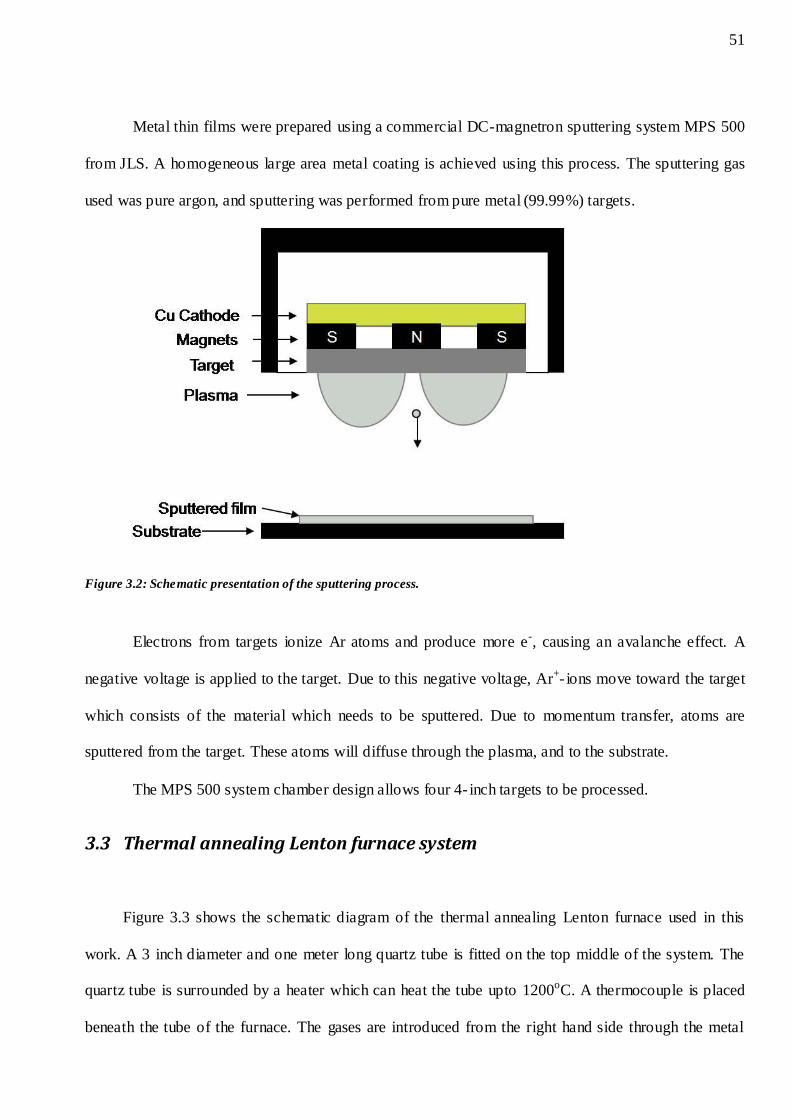
51
Metal thin films were prepared using a commercial DC-magnetron sputtering system MPS 500
from JLS. A homogeneous large area metal coating is achieved using this process. The sputtering gas
used was pure argon, and sputtering was performed from pure metal (99.99%) targets.
Figure 3.2: Schematic presentation of the sputtering process.
Electrons from targets ionize Ar atoms and produce more e-, causing an avalanche effect. A
negative voltage is applied to the target. Due to this negative voltage, Ar+- ions move toward the target
which consists of the material which needs to be sputtered. Due to momentum transfer, atoms are
sputtered from the target. These atoms will diffuse through the plasma, and to the substrate.
The MPS 500 system chamber design allows four 4- inch targets to be processed.
3.3 Thermal annealing Lenton furnace system
Figure 3.3 shows the schematic diagram of the thermal annealing Lenton furnace used in this
work. A 3 inch diameter and one meter long quartz tube is fitted on the top middle of the system. The
quartz tube is surrounded by a heater which can heat the tube upto 1200oC. A thermocouple is placed
beneath the tube of the furnace. The gases are introduced from the right hand side through the metal
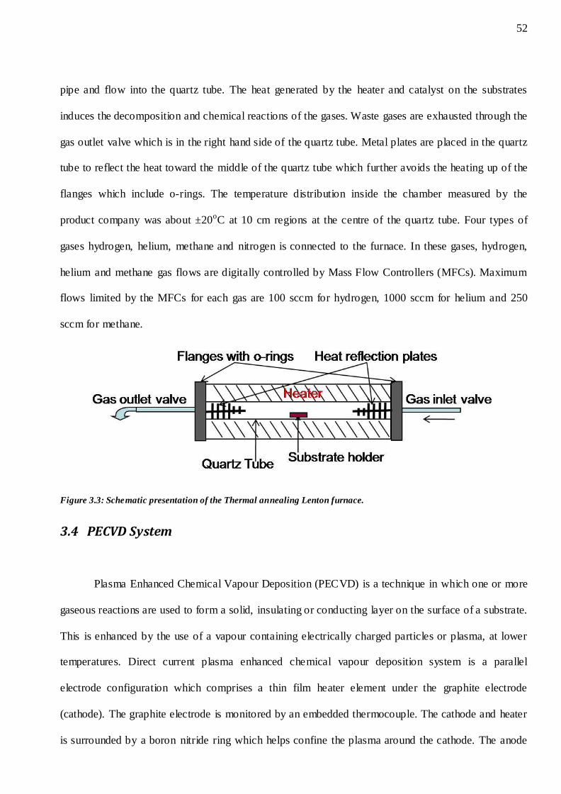
52
pipe and flow into the quartz tube. The heat generated by the heater and catalyst on the substrates
induces the decomposition and chemical reactions of the gases. Waste gases are exhausted through the
gas outlet valve which is in the right hand side of the quartz tube. Metal plates are placed in the quartz
tube to reflect the heat toward the middle of the quartz tube which further avoids the heating up of the
flanges which include o-rings. The temperature distribution inside the chamber measured by the
product company was about ±20oC at 10 cm regions at the centre of the quartz tube. Four types of
gases hydrogen, helium, methane and nitrogen is connected to the furnace. In these gases, hydrogen,
helium and methane gas flows are digitally controlled by Mass Flow Controllers (MFCs). Maximum
flows limited by the MFCs for each gas are 100 sccm for hydrogen, 1000 sccm for helium and 250
sccm for methane.
Figure 3.3: Schematic presentation of the Thermal annealing Lenton furnace.
3.4 PECVD System
Plasma Enhanced Chemical Vapour Deposition (PECVD) is a technique in which one or more
gaseous reactions are used to form a solid, insulating or conducting layer on the surface of a substrate.
This is enhanced by the use of a vapour containing electrically charged particles or plasma, at lower
temperatures. Direct current plasma enhanced chemical vapour deposition system is a parallel
electrode configuration which comprises a thin film heater element under the graphite electrode
(cathode). The graphite electrode is monitored by an embedded thermocouple. The cathode and heater
is surrounded by a boron nitride ring which helps confine the plasma around the cathode. The anode
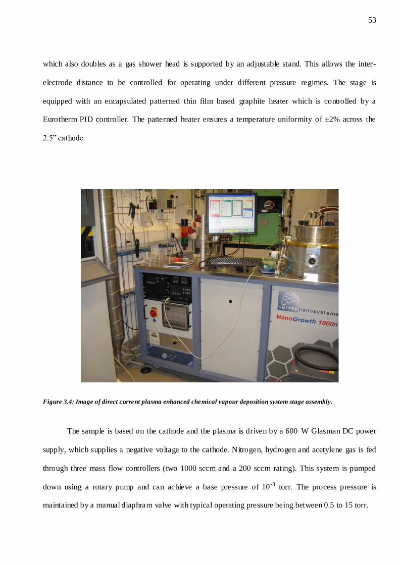
53
which also doubles as a gas shower head is supported by an adjustable stand. This allows the inter-
electrode distance to be controlled for operating under different pressure regimes. The stage is
equipped with an encapsulated patterned thin film based graphite heater which is controlled by a
Eurotherm PID controller. The patterned heater ensures a temperature uniformity of ±2% across the
2.5‖ cathode.
Figure 3.4: Image of direct current plasma enhanced chemical vapour deposition system stage assembly.
The sample is based on the cathode and the plasma is driven by a 600 W Glasman DC power
supply, which supplies a negative voltage to the cathode. Nitrogen, hydrogen and acetylene gas is fed
through three mass flow controllers (two 1000 sccm and a 200 sccm rating). This system is pumped
down using a rotary pump and can achieve a base pressure of 10-3 torr. The process pressure is
maintained by a manual diaphram valve with typical operating pressure being between 0.5 to 15 torr.

54
A typical run would start by placing the sample on the cathode electrode and evacuating the
chamber with the rotary pump to base pressure. The chamber is then backfilled with the carrier or
dilution gas to the desired pressure. If required, the temperature is raised before the plasma is ignited.
Acetylene is introduced only after the plasma is ignited. After the deposition is carried out, the sample
is allowed to cool down in nitrogen ambient before removal.
3.5 Inductively Coupled Plasma (ICP-RIE) Etching
To produce the SiNWs by the top-down approach, Si wafers are dry etched through with an ICP-
RIE system. A ICP-RIE system is preferred for this work due to the requirement of anisotropic etching
with vertical profile, lower etch rates and less surface damage. A STS ICP-RIE system has been used
in this work. The ICP-RIE system is the most commonly plasma based etching system, where ion
bombardment and chemical reactions occur. A photograph of the STS ICP-RIE system, which has
been used in this project, is shown in figure 3.5. A high chemical sensitivity with high etch rate is the
main advantage of ICP-RIE system.
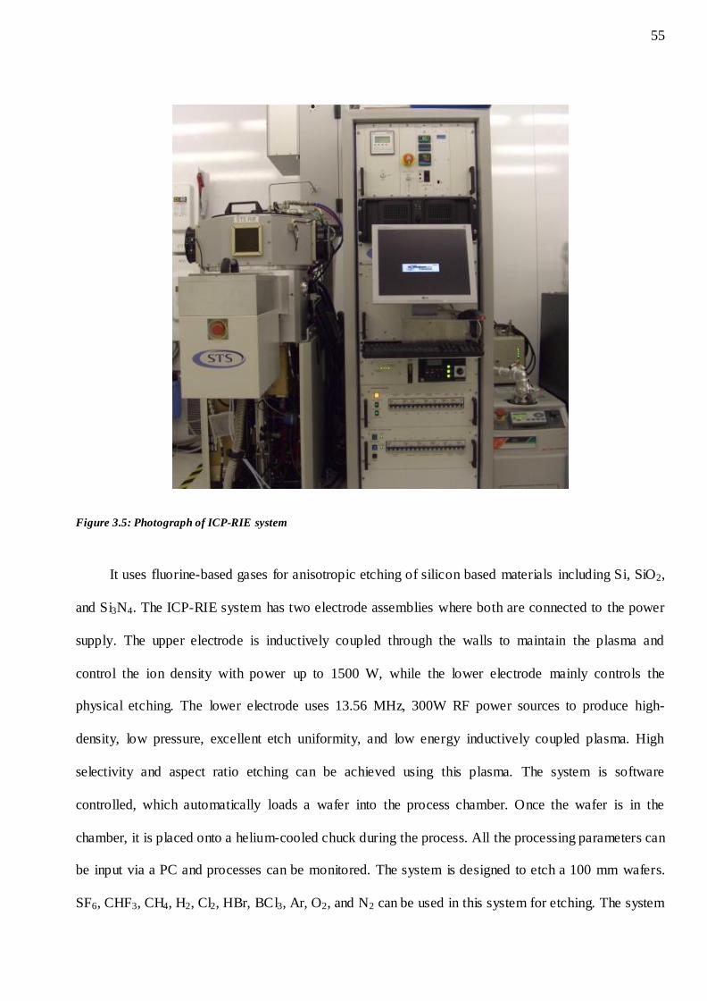
55
Figure 3.5: Photograph of ICP-RIE system
It uses fluorine-based gases for anisotropic etching of silicon based materials including Si, SiO2,
and Si3N4. The ICP-RIE system has two electrode assemblies where both are connected to the power
supply. The upper electrode is inductively coupled through the walls to maintain the plasma and
control the ion density with power up to 1500 W, while the lower electrode mainly controls the
physical etching. The lower electrode uses 13.56 MHz, 300W RF power sources to produce high-
density, low pressure, excellent etch uniformity, and low energy inductively coupled plasma. High
selectivity and aspect ratio etching can be achieved using this plasma. The system is software
controlled, which automatically loads a wafer into the process chamber. Once the wafer is in the
chamber, it is placed onto a helium-cooled chuck during the process. All the processing parameters can
be input via a PC and processes can be monitored. The system is designed to etch a 100 mm wafers.
SF6, CHF3, CH4, H2, Cl2, HBr, BCl3, Ar, O2, and N2 can be used in this system for etching. The system
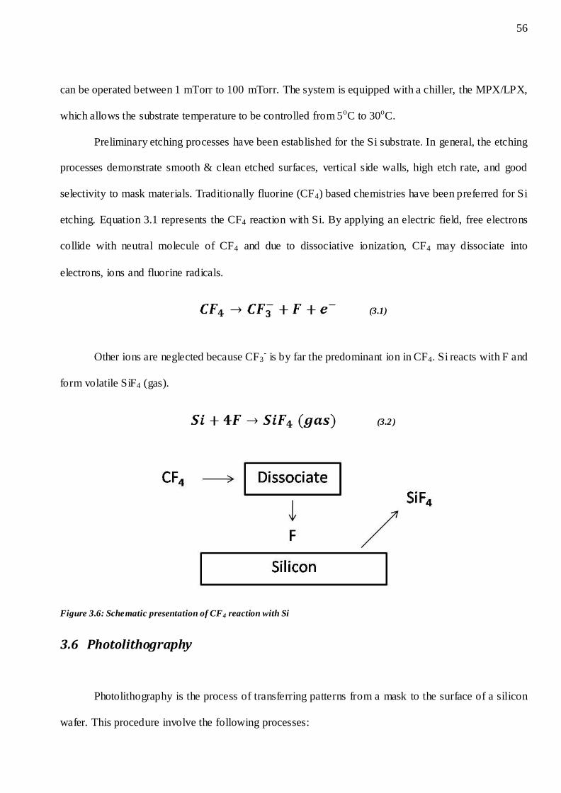
56
can be operated between 1 mTorr to 100 mTorr. The system is equipped with a chiller, the MPX/LPX,
which allows the substrate temperature to be controlled from 5oC to 30oC.
Preliminary etching processes have been established for the Si substrate. In general, the etching
processes demonstrate smooth & clean etched surfaces, vertical side walls, high etch rate, and good
selectivity to mask materials. Traditionally fluorine (CF4) based chemistries have been preferred for Si
etching. Equation 3.1 represents the CF4 reaction with Si. By applying an electric field, free electrons
collide with neutral molecule of CF4 and due to dissociative ionization, CF4 may dissociate into
electrons, ions and fluorine radicals.
(3.1)
Other ions are neglected because CF3- is by far the predominant ion in CF4. Si reacts with F and
form volatile SiF4 (gas).
(3.2 )
Figure 3.6: Schematic presentation of CF4 reaction with Si
3.6 Photolithography
Photolithography is the process of transferring patterns from a mask to the surface of a silicon
wafer. This procedure involve the following processes:
57
Wafer Cleaning: The silicon wafer is chemically cleaned using the standard cleaning process prior to
use in photolithography. A wafer is cleaned with acetone then isopropanol and then methanol which at
the end is cleaned with pure water and dried from N2 gas.
Metal deposition: A JLS 500 sputtering system has been used to deposit the required metal layer on
the Si wafer. Cr (10 nm)/Au (80 nm) was deposited on 300 nm oxidized silicon wafer. An under layer
of chromium is used to avoid delamination of the films.
Photoresist Application: Photoresist is a UV sensitive layer. The photoresist layer is applied with a
spinner which has a wafer chuck in the middle of the chamber. A spinner has a control unit which can
control the rotation speed as well as acceleration. A primer allows good adhesion between the
photoresist and the wafer surface. The wafer is removed from the chuck and put on a heater at 100oC
for 2 minutes to semi-harden the photoresist. Spin coating produces a thin uniform layer of photoresist
on the wafer surface. Shipley S1805 was used as the photoresist in this work.
Mask Alignment and Exposure: A photo mask is made of square glass plate. It has patterned metal on
one side. A Quintel Q7000 6‖ mask aligner was used in this work. The mask is aligned with the wafer
for transferring the pattern onto the wafer. After alignment, the photoresist is exposed to UV radiation
through the pattern on the mask with a high intensity UV light.
Development: The photoresist was developed in MF319 developer for 30 seconds, and then immersed
in DI water.
Hard Bake: This was done at 130oC for 30 minutes. Hard baking improves the adhesion of the
photoresist to the wafer surface and hardens the photoresist.
Etching: Wet etching was used to remove the regions of underlying material not protected by
photoresist after development. Wet etching of gold was done with the etchant KI:I2 :H2O (with
concentration 20gm:5ml:200ml) solution. Chromium etching was done with HCl. Finally, the wafer
was washed in acetone to remove the photoresist.

58
3.7 Scanning Electron Microscopy
The SEM is typically used to study the surface or near surface structure of bulk samples. A FEI
Quanta 200F Field emission SEM has been used for analyzing our samples. It is a versatile high
resolution (near 1 nm), low vacuum scanning electron microscope which can work with three modes
(high vacuum, low vacuum and ESEM). The SEM produces a magnified image of the specimen using
an electron beam. Its principle operation is shown in the figure 3.7. The electron gun, placed on the top
of the SEM system, produces a beam of monochromatic electrons. This electron beam follows the
vertical path through the microscope. Electromagnetic fields and lenses focuses the beam onto the
sample. It reduces the spot size of the electron beam typically to 2 – 10 nm in diameter. When this
electron beam hits the sample, low energy secondary electrons with other radiations (such as
backscattered electrons, X-ray) are ejected, which are then analyzed through the detectors. Using the
scan coils the electron beam is rastered across the specimen of which area gives the magnification of
the obtaining image. The rastering of the electron beam and secondary electron detector are used to
form the image.
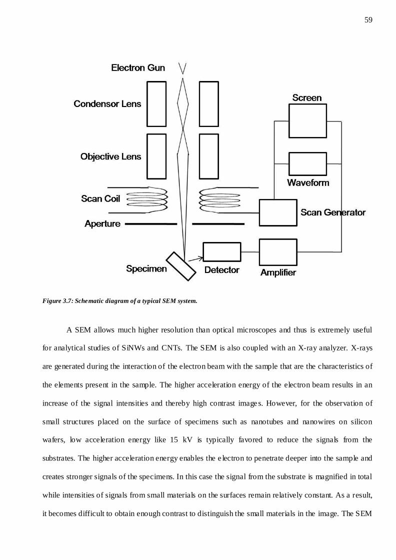
59
Figure 3.7: Schematic diagram of a typical SEM system.
A SEM allows much higher resolution than optical microscopes and thus is extremely useful
for analytical studies of SiNWs and CNTs. The SEM is also coupled with an X-ray analyzer. X-rays
are generated during the interaction of the electron beam with the sample that are the characteristics of
the elements present in the sample. The higher acceleration energy of the electron beam results in an
increase of the signal intensities and thereby high contrast images. However, for the observation of
small structures placed on the surface of specimens such as nanotubes and nanowires on silicon
wafers, low acceleration energy like 15 kV is typically favored to reduce the signals from the
substrates. The higher acceleration energy enables the e lectron to penetrate deeper into the sample and
creates stronger signals of the specimens. In this case the signal from the substrate is magnified in total
while intensities of signals from small materials on the surfaces remain relatively constant. As a result,
it becomes difficult to obtain enough contrast to distinguish the small materials in the image. The SEM
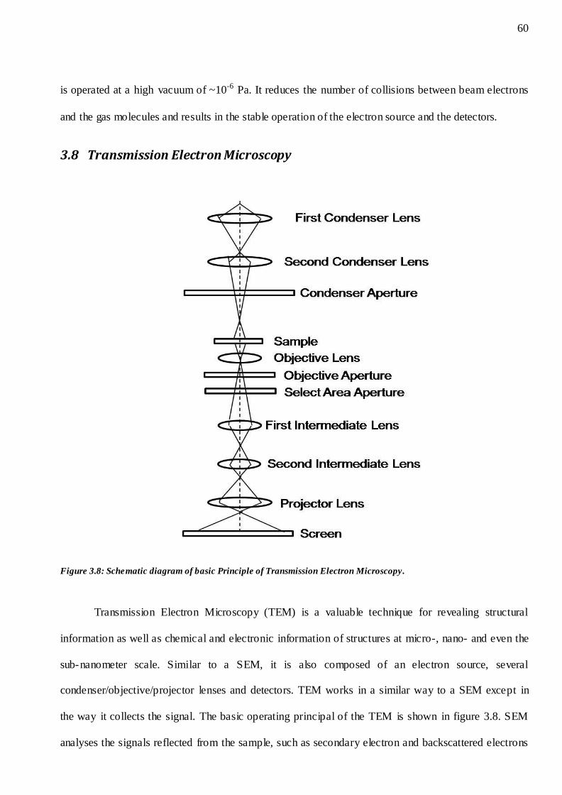
60
is operated at a high vacuum of ~10-6 Pa. It reduces the number of collisions between beam electrons
and the gas molecules and results in the stable operation of the electron source and the detectors.
3.8 Transmission Electron Microscopy
Figure 3.8: Schematic diagram of basic Principle of Transmission Electron Microscopy.
Transmission Electron Microscopy (TEM) is a valuable technique for revealing structural
information as well as chemical and electronic information of structures at micro-, nano- and even the
sub-nanometer scale. Similar to a SEM, it is also composed of an electron source, several
condenser/objective/projector lenses and detectors. TEM works in a similar way to a SEM except in
the way it collects the signal. The basic operating principal of the TEM is shown in figure 3.8. SEM
analyses the signals reflected from the sample, such as secondary electron and backscattered electrons
61
while in a TEM the analysis of electrons is of the component through the specimen. When a beam of
electrons passes through the sample, wherever part is transmitted is projected onto phosphor screen.
This yields information on the morphology such as the size, shape and arrangements of the particles
which make up the sample as well as their relationship to each other on the scale of atomic diameters.
It also yields crystallographic information such as the arrangements of atoms in the specimen and their
degree of order, detection of atomic-scale defects in areas a few nanometers in diameter.
To obtain a good signal and clear images, the thickness of the sample should be very small, e.g.
less than 100 nm in thickness. The acceleration energy of the electron gun is much higher (~200 kV)
than that of a SEM resulting in increased spatial resolution. A Philips CM200 with LaB6 source, 200 k
eV acceleration voltage with 0.17 nm resolution has been used in this work.
3.9 Raman Spectroscopy
Raman spectroscopy is important for chemical analysis of the samples. It depends on the
Raman Effect and enables the characterization of samples in a non-destructive manner and requires
simple sample preparation. Raman spectroscopy was performed using a Renishaw 2000 Raman
microscope with two possible excitation sources of a 782 nm and 514 nm, in all the analysis done in
this work.
Raman Effect
When monochromatic radiation is incident on a molecule then most photons are elastically
scattered. A small fraction of photon (~1 in 107 photons) is inelastically scattered, and its frequency is
different from the incident photon. The difference between the frequencies is determined by the
material on which light was incident. The effect which leads to this ine lastic scatter is called the
Raman effect. The difference in energy between incident photon and scattered photon is the energy of
the vibrational state of the molecule.
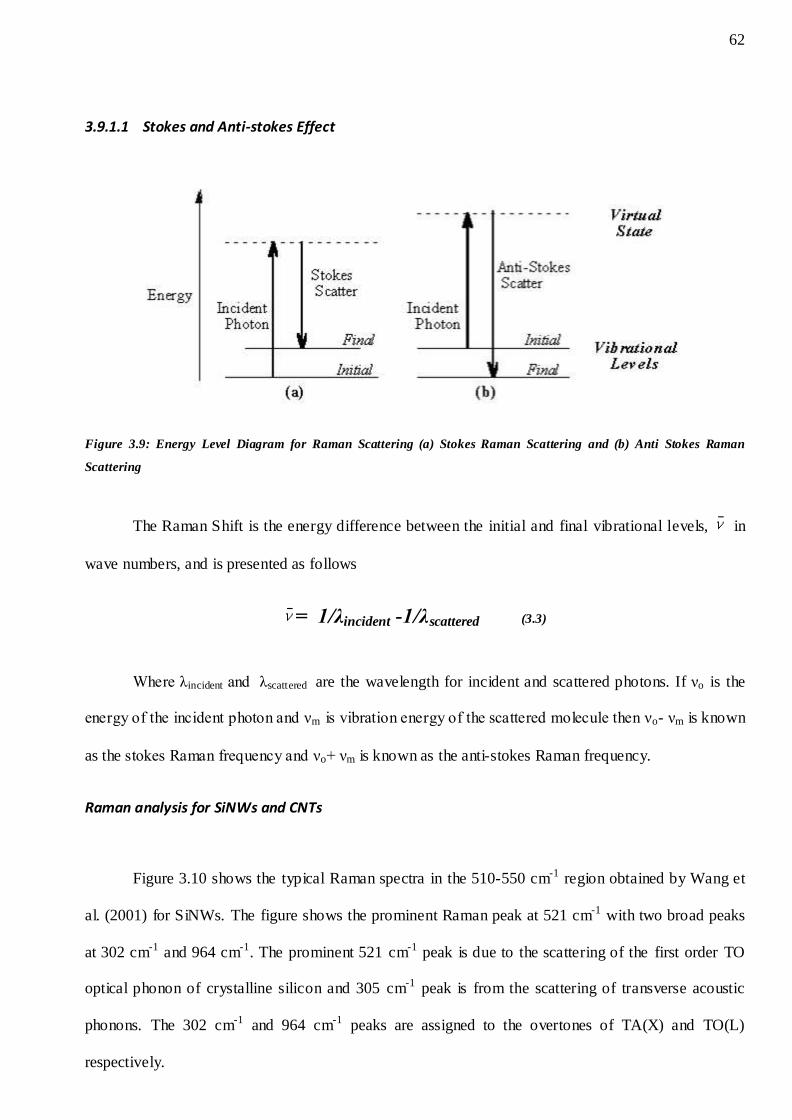
62
3.9.1.1 Stokes and Anti-stokes Effect
Figure 3.9: Energy Level Diagram for Raman Scattering (a) Stokes Raman Scattering and (b) Anti Stokes Raman
Scattering
The Raman Shift is the energy difference between the initial and final vibrational levels, in
wave numbers, and is presented as follows
= 1/λincident -1/λscattered (3.3)
Where λincident and λscattered are the wavelength for incident and scattered photons. If νo is the
energy of the incident photon and νm is vibration energy of the scattered molecule then νo- νm is known
as the stokes Raman frequency and νo+ νm is known as the anti-stokes Raman frequency.
Raman analysis for SiNWs and CNTs
Figure 3.10 shows the typical Raman spectra in the 510-550 cm-1 region obtained by Wang et
al. (2001) for SiNWs. The figure shows the prominent Raman peak at 521 cm-1 with two broad peaks
at 302 cm-1 and 964 cm-1. The prominent 521 cm-1 peak is due to the scattering of the first order TO
optical phonon of crystalline silicon and 305 cm-1 peak is from the scattering of transverse acoustic
phonons. The 302 cm-1 and 964 cm-1 peaks are assigned to the overtones of TA(X) and TO(L)
respectively.
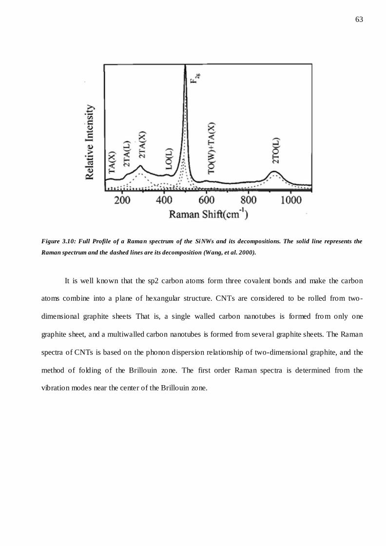
63
Figure 3.10: Full Profile of a Raman spectrum of the SiNWs and its decompositions. The solid line represents the
Raman spectrum and the dashed lines are its decomposition (Wang, et al. 2000).
It is well known that the sp2 carbon atoms form three covalent bonds and make the carbon
atoms combine into a plane of hexangular structure. CNTs are considered to be rolled from two-
dimensional graphite sheets That is, a single walled carbon nanotubes is formed from only one
graphite sheet, and a multiwalled carbon nanotubes is formed from several graphite sheets. The Raman
spectra of CNTs is based on the phonon dispersion relationship of two-dimensional graphite, and the
method of folding of the Brillouin zone. The first order Raman spectra is determined from the
vibration modes near the center of the Brillouin zone.
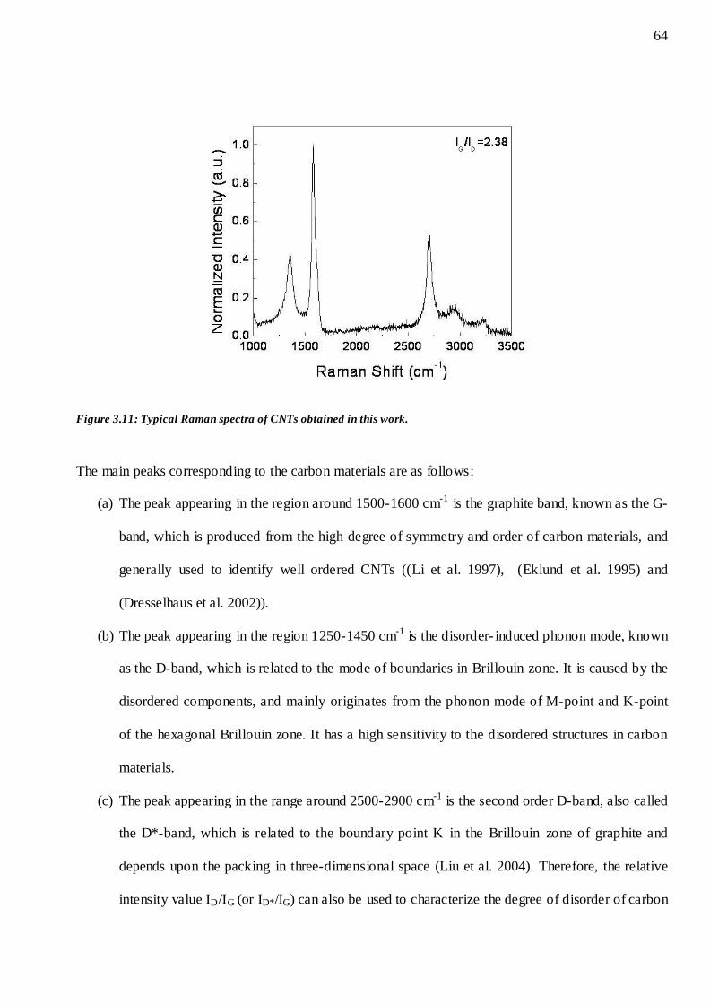
64
Figure 3.11: Typical Raman spectra of CNTs obtained in this work.
The main peaks corresponding to the carbon materials are as follows:
(a) The peak appearing in the region around 1500-1600 cm-1 is the graphite band, known as the G-
band, which is produced from the high degree of symmetry and order of carbon materials, and
generally used to identify well ordered CNTs ((Li et al. 1997), (Eklund et al. 1995) and
(Dresselhaus et al. 2002)).
(b) The peak appearing in the region 1250-1450 cm-1 is the disorder- induced phonon mode, known
as the D-band, which is related to the mode of boundaries in Brillouin zone. It is caused by the
disordered components, and mainly originates from the phonon mode of M-point and K-point
of the hexagonal Brillouin zone. It has a high sensitivity to the disordered structures in carbon
materials.
(c) The peak appearing in the range around 2500-2900 cm-1 is the second order D-band, also called
the D*-band, which is related to the boundary point K in the Brillouin zone of graphite and
depends upon the packing in three-dimensional space (Liu et al. 2004). Therefore, the relative
intensity value ID/IG (or ID*/IG) can also be used to characterize the degree of disorder of carbon
65
materials, i.e., smaller ratio of ID/IG or larger of ID*/IG corresponding to the higher order degree
of substances, such as CNTs.
(d) The peaks at 2875 cm-1, 2987 cm-1 and 3146 cm-1 are due to symmetric and asymmetric-H
stretch vibrations of the CH3 group and asymmetric C-H stretch vibrations of the CH2 group,
respectively (Liu et al. 2004).
Typical Raman spectra obtained for CNTs in this work has been shown in figure 3.11. According
to these peaks, the larger D* peak and larger IG/ID ratio or smaller IG/I D* ratio indicates that the CNTs
grown with this sample have higher degrees of order and graphitization.
3.10 Summary
The experimental and analysis techniques, used in this work have been discussed in this
chapter. The deposition and synthesis techniques for SiNWs, CNTs and HJs has been discussed in the
earlier part of this chapter, which includes DC-Magnetron sputtering, thermal annealing, PECVD and
Inductively coupled plasma etching (ICP-RIE) techniques. Then discussion moved towards the device
fabrication process, photolithography, following with discussions of analysis techniques for material
analysis. It includes Scanning electron microscopy (SEM) and Transmission electron microscopy
(TEM) which are typically used to image physical dimensions of the materials and then at the end of
the chapter, Raman spectroscopy, which is used to obtain information about the chemical structure
contained within the materials, is explained.
66
4 Silicon Nanowires Synthesis
We present the synthesis of silicon nanowires by combining a SLS mechanism with a VLS
mechanism in this work. This method does not need a complicated experimental setup or the use of the
hazardous gas silane. It is a growth method which is cost-effective, large-area-compatible and may
give a higher degree of control of the end product, facilitated by a simple experimental process. In the
VLS mechanism, a gold-coated silicon wafer is used as a substrate and a Si precursor is thermally
degraded from the gas phase over the substrate whilst the Au film breaks up into islands. The Si from
the precursor dissolves into the gold droplets to form eutectic gold silicide, until it supersaturates the
catalyst. Upon saturation, Si extrudes from the droplets as nanowires. In the SLS mechanism (Lee,
Yang et al. 2004; Lee and et al. 2008), the Si wafer itself acts as the silicon source in the growth and Si
nanowires grow by thermal annealing, assisted by the transition metal coating on the silicon wafer.
These mechanisms have the advantage of controlling the nanowire diameter through the size of the
nucleating metal island. Our synthesis method combines the SLS mechanism for the initial formation
of metal islands (Au or Ni), their saturation with Si and the extrusion of nanowire growth, which is
then sustained via a VLS mechanism and published by Sharma et al. (2010).
A set of experiments was designed in order to produce silicon nanowires using the thermal
annealing method. Two types of growth are methodologies studied in this research to grow SiNWs are
explained in this thesis. One growth process produces silicon oxide nanowires with a nickel silicide tip
and crystalline Si tail which ends with long silicon oxide nanowires. We will explain this growth in
Section 4.1 ―Silicon oxide nanowire growth‖. The second growth process gives SiNWs with
crystalline Si core and oxide clad, headed with a silicide tip. We will explain this growth process in
Section 4.2 ―Crystalline core-clad SiNW growth‖. Crystalline silicon nanowires have been grown with
this method. This nanowire has a Si-core and oxide-clad structure. Oxide clad has been shown to have
applications in fabricating surround-gate field effect transistors (Ng, Han et al. 2004). The
experimental procedures for these methodologies are described in this chapter. The top-down approach
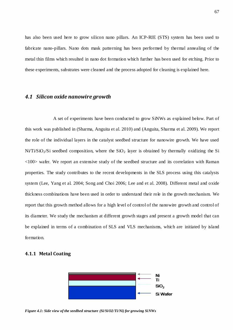
67
has also been used here to grow silicon nano pillars. An ICP-RIE (STS) system has been used to
fabricate nano-pillars. Nano dots mask patterning has been performed by thermal annealing of the
metal thin films which resulted in nano dot formation which further has been used for etching. Prior to
these experiments, substrates were cleaned and the process adopted for cleaning is explained here.
4.1 Silicon oxide nanowire growth
A set of experiments have been conducted to grow SiNWs as explained below. Part of
this work was published in (Sharma, Anguita et al. 2010) and (Anguita, Sharma et al. 2009). We report
the role of the individual layers in the catalyst seedbed structure for nanowire growth. We have used
Ni/Ti/SiO2/Si seedbed composition, where the SiO2 layer is obtained by thermally oxidizing the Si
<100> wafer. We report an extensive study of the seedbed structure and its correlation with Raman
properties. The study contributes to the recent developments in the SLS process using this catalysts
system (Lee, Yang et al. 2004; Song and Choi 2006; Lee and et al. 2008). Different metal and oxide
thickness combinations have been used in order to understand their role in the growth mechanism. We
report that this growth method allows for a high level of control of the nanowire growth and control of
its diameter. We study the mechanism at different growth stages and present a growth model that can
be explained in terms of a combination of SLS and VLS mechanisms, which are initiated by island
formation.
4.1.1 Metal Coating
Figure 4.1: Side view of the seedbed structure (Si/SiO2/Ti/Ni) for growing SiNWs

68
Table 4.1: Seedbed structure with different thicknesses of catalyst/substrate layers to conduct a combinatorial study of
SiNW growth.
The metal seedbed layer deposition was performed using a DC-magnetron sputtering system
(JLS), using argon at a pressure of 5 mTorr with 25 sccm flow rate. The substrates were p-type <100>
single crystal Si, and thermally-oxidised silicon (50 nm and 100 nm thick oxide layers). Various
thicknesses of Ni [0 nm, 10 nm, 20 nm, 30 nm] were deposited on layers of Ti [0 nm, 20 nm, 50 nm,
100 nm and 200 nm], with the Ni always on the top to make our experimental matrix, which is shown
in table 1. The side view of the seedbed structure of Si/SiO2/Ti/Ni is shown in figure 4.1.
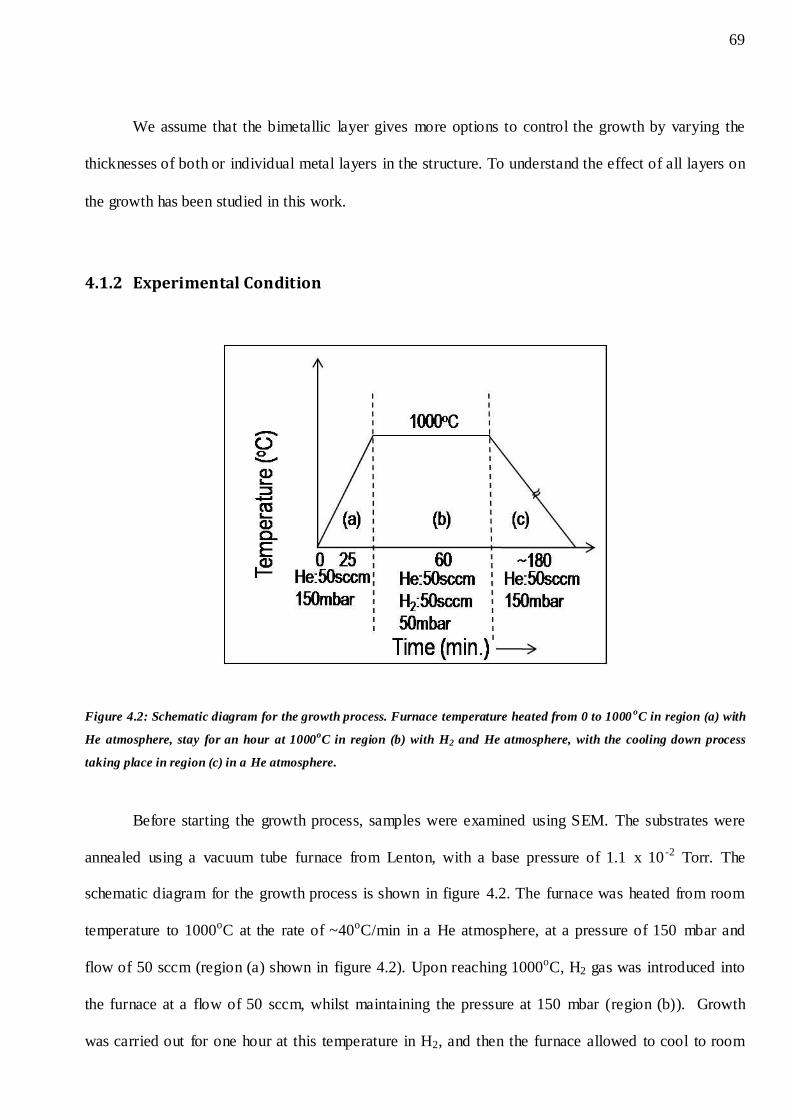
69
We assume that the bimetallic layer gives more options to control the growth by varying the
thicknesses of both or individual metal layers in the structure. To understand the effect of all layers on
the growth has been studied in this work.
4.1.2 Experimental Condition
Figure 4.2: Schematic diagram for the growth process. Furnace temperature heated from 0 to 1000oC in region (a) with
He atmosphere, stay for an hour at 1000oC in region (b) with H2 and He atmosphere, with the cooling down process
taking place in region (c) in a He atmosphere.
Before starting the growth process, samples were examined using SEM. The substrates were
annealed using a vacuum tube furnace from Lenton, with a base pressure of 1.1 x 10 -2 Torr. The
schematic diagram for the growth process is shown in figure 4.2. The furnace was heated from room
temperature to 1000oC at the rate of ~40oC/min in a He atmosphere, at a pressure of 150 mbar and
flow of 50 sccm (region (a) shown in figure 4.2). Upon reaching 1000oC, H2 gas was introduced into
the furnace at a flow of 50 sccm, whilst maintaining the pressure at 150 mbar (region (b)). Growth
was carried out for one hour at this temperature in H2, and then the furnace allowed to cool to room
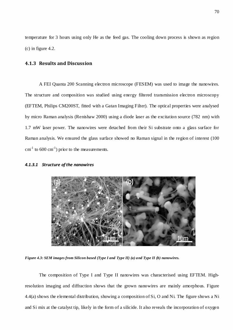
70
temperature for 3 hours using only He as the feed gas. The cooling down process is shown as region
(c) in figure 4.2.
4.1.3 Results and Discussion
A FEI Quanta 200 Scanning electron microscope (FESEM) was used to image the nanowires.
The structure and composition was studied using energy filtered transmission electron microscopy
(EFTEM, Philips CM200ST, fitted with a Gatan Imaging Filter). The optical properties were analysed
by micro Raman analysis (Renishaw 2000) using a diode laser as the excitation source (782 nm) with
1.7 mW laser power. The nanowires were detached from their Si substrate onto a glass surface for
Raman analysis. We ensured the glass surface showed no Raman signal in the region of interest (100
cm-1 to 600 cm-1) prior to the measurements.
4.1.3.1 Structure of the nanowires
Figure 4.3: SEM images from Silicon based (Type I and Type II) (a) and Type II (b) nanowires.
The composition of Type I and Type II nanowires was characterised using EFTEM. High-
resolution imaging and diffraction shows that the grown nanowires are mainly amorphous. Figure
4.4(a) shows the elemental distribution, showing a composition of Si, O and Ni. The figure shows a Ni
and Si mix at the catalyst tip, likely in the form of a silicide. It also reveals the incorporation of oxygen
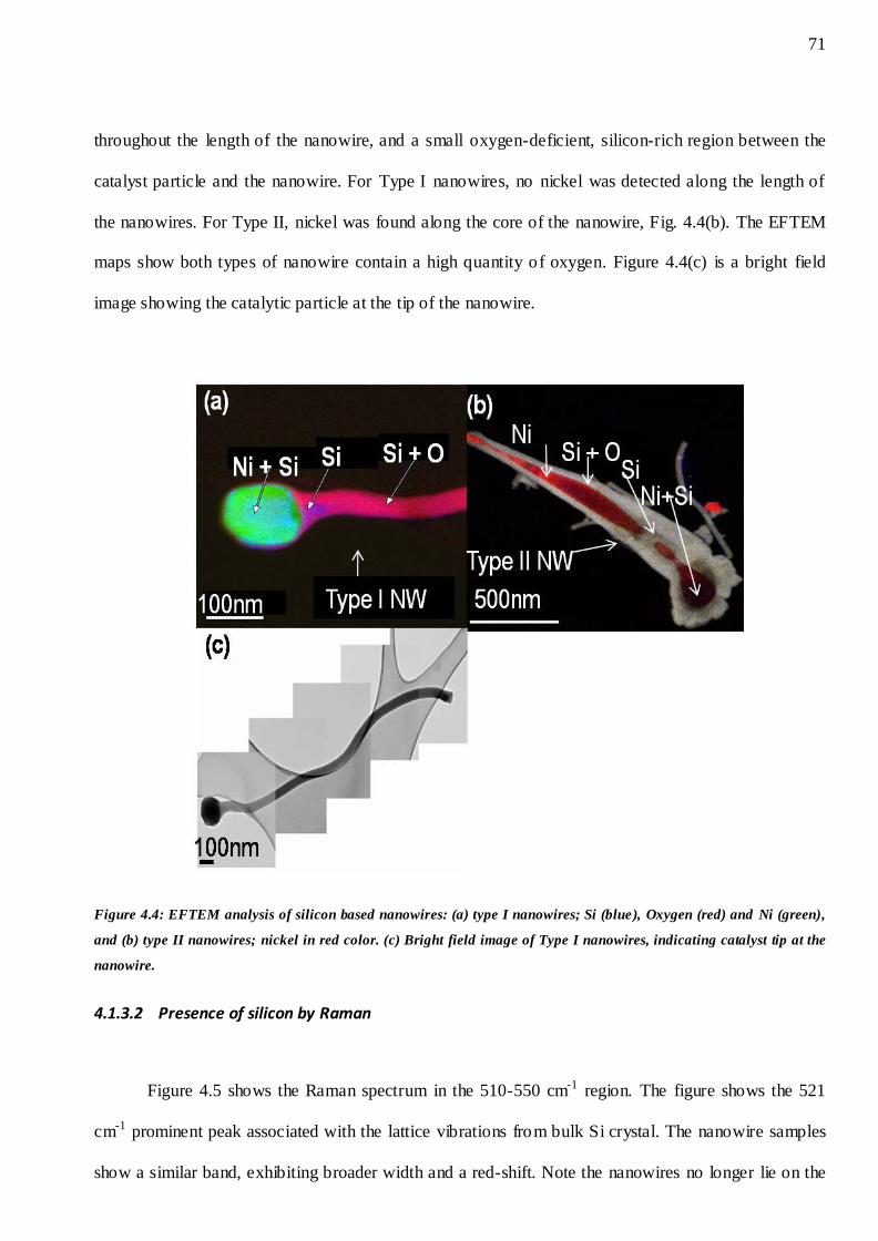
71
throughout the length of the nanowire, and a small oxygen-deficient, silicon-rich region between the
catalyst particle and the nanowire. For Type I nanowires, no nickel was detected along the length of
the nanowires. For Type II, nickel was found along the core of the nanowire, Fig. 4.4(b). The EFTEM
maps show both types of nanowire contain a high quantity of oxygen. Figure 4.4(c) is a bright field
image showing the catalytic particle at the tip of the nanowire.
Figure 4.4: EFTEM analysis of silicon based nanowires: (a) type I nanowires; Si (blue), Oxygen (red) and Ni (green),
and (b) type II nanowires; nickel in red color. (c) Bright field image of Type I nanowires, indicating catalyst tip at the
nanowire.
4.1.3.2 Presence of silicon by Raman
Figure 4.5 shows the Raman spectrum in the 510-550 cm-1 region. The figure shows the 521
cm-1 prominent peak associated with the lattice vibrations from bulk Si crystal. The nanowire samples
show a similar band, exhibiting broader width and a red-shift. Note the nanowires no longer lie on the
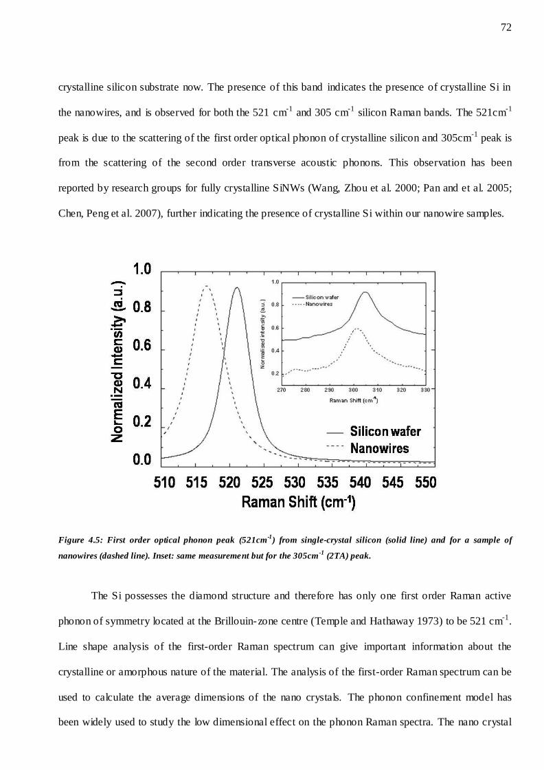
72
crystalline silicon substrate now. The presence of this band indicates the presence of crystalline Si in
the nanowires, and is observed for both the 521 cm-1 and 305 cm-1 silicon Raman bands. The 521cm-1
peak is due to the scattering of the first order optical phonon of crystalline silicon and 305cm-1 peak is
from the scattering of the second order transverse acoustic phonons. This observation has been
reported by research groups for fully crystalline SiNWs (Wang, Zhou et al. 2000; Pan and et al. 2005;
Chen, Peng et al. 2007), further indicating the presence of crystalline Si within our nanowire samples.
Figure 4.5: First order optical phonon peak (521cm-1
) from single-crystal silicon (solid line) and for a sample of
nanowires (dashed line). Inset: same measurement but for the 305cm-1
(2TA) peak.
The Si possesses the diamond structure and therefore has only one first order Raman active
phonon of symmetry located at the Brillouin-zone centre (Temple and Hathaway 1973) to be 521 cm-1.
Line shape analysis of the first-order Raman spectrum can give important information about the
crystalline or amorphous nature of the material. The analysis of the first-order Raman spectrum can be
used to calculate the average dimensions of the nano crystals. The phonon confinement model has
been widely used to study the low dimensional effect on the phonon Raman spectra. The nano crystal
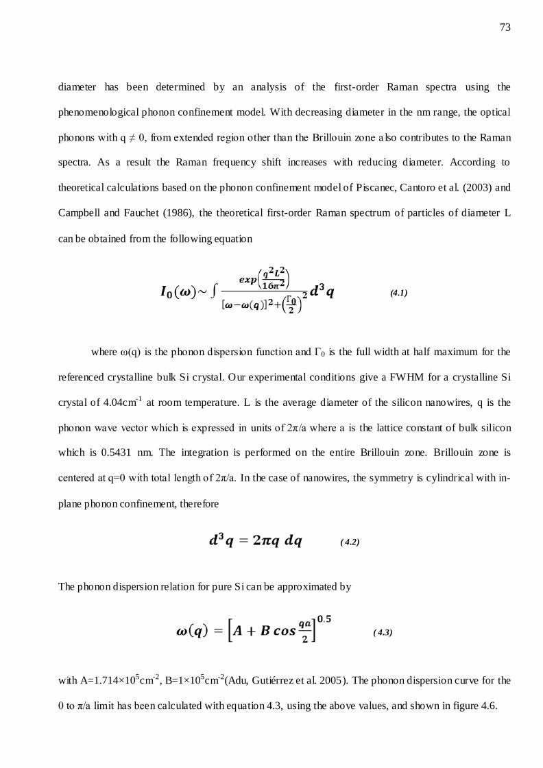
73
diameter has been determined by an analysis of the first-order Raman spectra using the
phenomenological phonon confinement model. With decreasing diameter in the nm range, the optical
phonons with q ≠ 0, from extended region other than the Brillouin zone a lso contributes to the Raman
spectra. As a result the Raman frequency shift increases with reducing diameter. According to
theoretical calculations based on the phonon confinement model of Piscanec, Cantoro et al. (2003) and
Campbell and Fauchet (1986), the theoretical first-order Raman spectrum of particles of diameter L
can be obtained from the following equation
(4.1)
where ω(q) is the phonon dispersion function and Г0 is the full width at half maximum for the
referenced crystalline bulk Si crystal. Our experimental conditions give a FWHM for a crystalline Si
crystal of 4.04cm-1 at room temperature. L is the average diameter of the silicon nanowires, q is the
phonon wave vector which is expressed in units of 2π/a where a is the lattice constant of bulk silicon
which is 0.5431 nm. The integration is performed on the entire Brillouin zone. Brillouin zone is
centered at q=0 with total length of 2π/a. In the case of nanowires, the symmetry is cylindrical with in-
plane phonon confinement, therefore
( 4.2)
The phonon dispersion relation for pure Si can be approximated by
( 4.3)
with A=1.714×105cm-2, B=1×105cm-2(Adu, Gutiérrez et al. 2005). The phonon dispersion curve for the
0 to π/a limit has been calculated with equation 4.3, using the above values, and shown in figure 4.6.
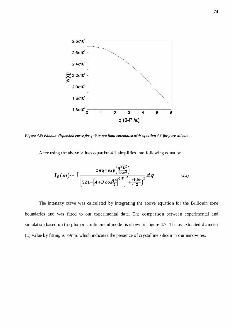
74
Figure 4.6: Phonon dispersion curve for q=0 to π/a limit calculated with equation 4.3 for pure silicon.
After using the above values equation 4.1 simplifies into following equation.
( 4.4)
The intensity curve was calculated by integrating the above equation for the Brillouin zone
boundaries and was fitted to our experimental data. The comparison between experimental and
simulation based on the phonon confinement model is shown in figure 4.7. The as-extracted diameter
(L) value by fitting is ~9nm, which indicates the presence of crystalline silicon in our nanowires.
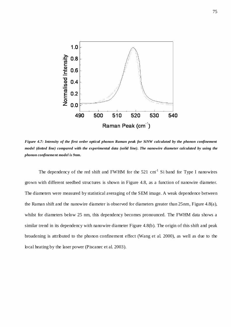
75
Figure 4.7: Intensity of the first order optical phonon Raman peak for SiNW calculated by the phonon confinement
model (dotted line) compared with the experimental data (solid line). The nanowire diameter calculated by using the
phonon confinement model is 9nm.
The dependency of the red shift and FWHM for the 521 cm-1 Si band for Type I nanowires
grown with different seedbed structures is shown in Figure 4.8, as a function of nanowire diameter.
The diameters were measured by statistical averaging of the SEM image. A weak dependence between
the Raman shift and the nanowire diameter is observed for diameters greater than 25nm, Figure 4.8(a),
whilst for diameters below 25 nm, this dependency becomes pronounced. The FWHM data shows a
similar trend in its dependency with nanowire diameter Figure 4.8(b). The origin of this shift and peak
broadening is attributed to the phonon confinement effect (Wang et al. 2000), as well as due to the
local heating by the laser power (Piscanec et al. 2003).
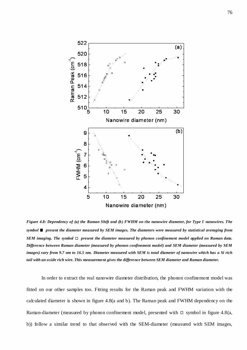
76
Figure 4.8: Dependency of (a) the Raman Shift and (b ) FWHM on the nanowire diameter, for Type I nanowires. The
symbol present the diameter measured by SEM images. The diameters were measured by statistical averaging from
SEM imaging. The symbol present the diameter measured by phonon confinement model applied on Raman data.
Difference between Raman diameter (measured by phonon confinement model) and SEM diameter (measured by SEM
images) vary from 9.7 nm to 16.5 nm. Diameter measured with SEM is total diameter of nanowire which has a Si rich
tail with an oxide rich wire. This measurement gives the difference between SEM diameter and Raman diameter.
In order to extract the real nanowire diameter distribution, the phonon confinement model was
fitted on our other samples too. Fitting results for the Raman peak and FWHM variation with the
calculated diameter is shown in figure 4.8(a and b). The Raman peak and FWHM dependency on the
Raman-diameter (measured by phonon confinement model, presented with symbol in figure 4.8(a,
b)) follow a similar trend to that observed with the SEM-diameter (measured with SEM images,
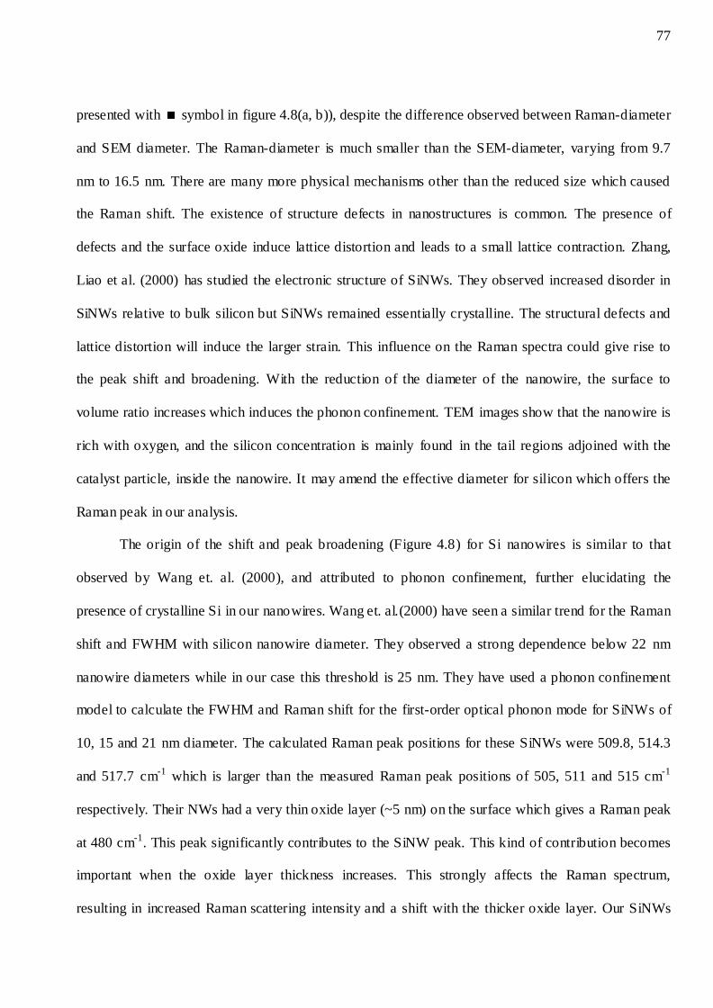
77
presented with symbol in figure 4.8(a, b)), despite the difference observed between Raman-diameter
and SEM diameter. The Raman-diameter is much smaller than the SEM-diameter, varying from 9.7
nm to 16.5 nm. There are many more physical mechanisms other than the reduced size which caused
the Raman shift. The existence of structure defects in nanostructures is common. The presence of
defects and the surface oxide induce lattice distortion and leads to a small lattice contraction. Zhang,
Liao et al. (2000) has studied the electronic structure of SiNWs. They observed increased disorder in
SiNWs relative to bulk silicon but SiNWs remained essentially crystalline. The structural defects and
lattice distortion will induce the larger strain. This influence on the Raman spectra could give rise to
the peak shift and broadening. With the reduction of the diameter of the nanowire, the surface to
volume ratio increases which induces the phonon confinement. TEM images show that the nanowire is
rich with oxygen, and the silicon concentration is mainly found in the tail regions adjoined with the
catalyst particle, inside the nanowire. It may amend the effective diameter for silicon which offers the
Raman peak in our analysis.
The origin of the shift and peak broadening (Figure 4.8) for Si nanowires is similar to that
observed by Wang et. al. (2000), and attributed to phonon confinement, further elucidating the
presence of crystalline Si in our nanowires. Wang et. al.(2000) have seen a similar trend for the Raman
shift and FWHM with silicon nanowire diameter. They observed a strong dependence below 22 nm
nanowire diameters while in our case this threshold is 25 nm. They have used a phonon confinement
model to calculate the FWHM and Raman shift for the first-order optical phonon mode for SiNWs of
10, 15 and 21 nm diameter. The calculated Raman peak positions for these SiNWs were 509.8, 514.3
and 517.7 cm-1 which is larger than the measured Raman peak positions of 505, 511 and 515 cm-1
respectively. Their NWs had a very thin oxide layer (~5 nm) on the surface which gives a Raman peak
at 480 cm-1. This peak significantly contributes to the SiNW peak. This kind of contribution becomes
important when the oxide layer thickness increases. This strongly affects the Raman spectrum,
resulting in increased Raman scattering intensity and a shift with the thicker oxide layer. Our SiNWs
78
have a thicker oxide layer compared to them and may affect the Raman peak intensity and shift in the
SiNWs. It is important to understand the cause of Raman shift and peak broadening in our samples.
Figure 4.9: Raman peak shift variation with incident laser power for SiNWs (Substrate = Ni=20nm; Ti=100nm; Oxide=
0nm). First order optical phonon peak shifts from 516.61 to 504.01 with increasing laser power from 0.17mW to 17mW.
The Raman peak for laser powers of 0.17mW and 1.7mW is similar.
Raman spectra for SiNWs (for Ni=20 nm; Ti=100 nm; Oxide=0 nm; nanowires diameter=22
nm) was recorded for different laser powers varying from 0.17 mW to 17 mW. When the sample is
illuminated with laser power from 0.17 mW, 1.7 mW, 4.25 mW, 8.5 mW and 17 mW, the first order
optical phonon peak is observed at 516.61 cm-1, 516.61 cm-1, 513.5 cm-1, 511.39 cm-1 and 504.01 cm-1
respectively (figure 4.9). For 0.17 mW and 1.7 mW laser powers, the Raman peak is observed at a
similar point while with increasing laser power from 1.7mW to 4.5mW, the Raman peak shifted from
516.61 cm-1 to 513.5 cm-1 (figure 4.9). Analysis indicates that the optical phonon peaks of silicon
nanowires are dependent on the excitation laser power. Thus, a low laser power is essential in order to
examine the phonon spectrum of different sized nanowires. A low laser power of 1.7 mW is used in
our analysis of samples. Wang, Zhou et al. (2000) also found a similar effect of laser heating on the
Raman shift which can be neglected for laser powers less than 2.5 mW, concluding that the laser
79
heating effect would not be comparable to the Raman shift due with the use of 1.7 mW laser power in
our samples. The Raman peak shift in our samples are therefore attributed to the crystalline silicon
presents in the nanowires.
4.1.3.3 Effect of seedbed structure on the nanowires
A clear and consistent dependency between the layers used in the seedbed structure and the
type of nanowire growth was observed and identified in Table 4.2. It shows that some layered
structures resulted in only Type I nanowire growth, whilst other compositions exhibited a mixture of
Type I and Type II nanowires. It was observed that the seedbed compositions with no nickel exhibited
no nanowire growth, indicating nickel is an essential component/ element of the growth. Concentration
of Type I and Type II nanowires has been calculated by determining the diameter statistics of ~100
NWs on each sample.
Table 4.2 reveals that either Ti or SiO2 or a combination of both is required to produce Type II
nanowires. Seedbed compositions of the form Ni/Ti/Si or Ni/Ti/SiO2/Si produce Type I and Type II
nanowires while Ni/Si structures produce only Type I nanowires. From the experimental observation,
it is clear that Type II nanowires occur as a result of the interaction between the Ti and the SiO 2 layers
with the Ni catalyst layer. The table also reveals that reducing the oxide layer thickness (while
maintaining Ti (100 nm) and Ni (20 nm) in the seedbed structure) results in an increase of Type I
nanowire concentration. i.e. diffusion of the Si through the SiO2 layer, which then mixes with Ti/ Ni is
key for the formation of Type I nanowires. For Ni/Ti/SiO2/Si substrates, a maximum concentration
(~98%) of Type I nanowires is achieved for 0 nm oxide. With lesser oxide thicknesses, Si diffusion
time through the SiO2 layer is less and favorable for nickel silicide formation which further forms
Type I nanowires. With increasing oxide thickness, the Si diffusion time through the SiO2 layer is
increased, and favorable for the formation of NixTiySiz compared to nickel silicide formation which
gives Type II nanowire growth.
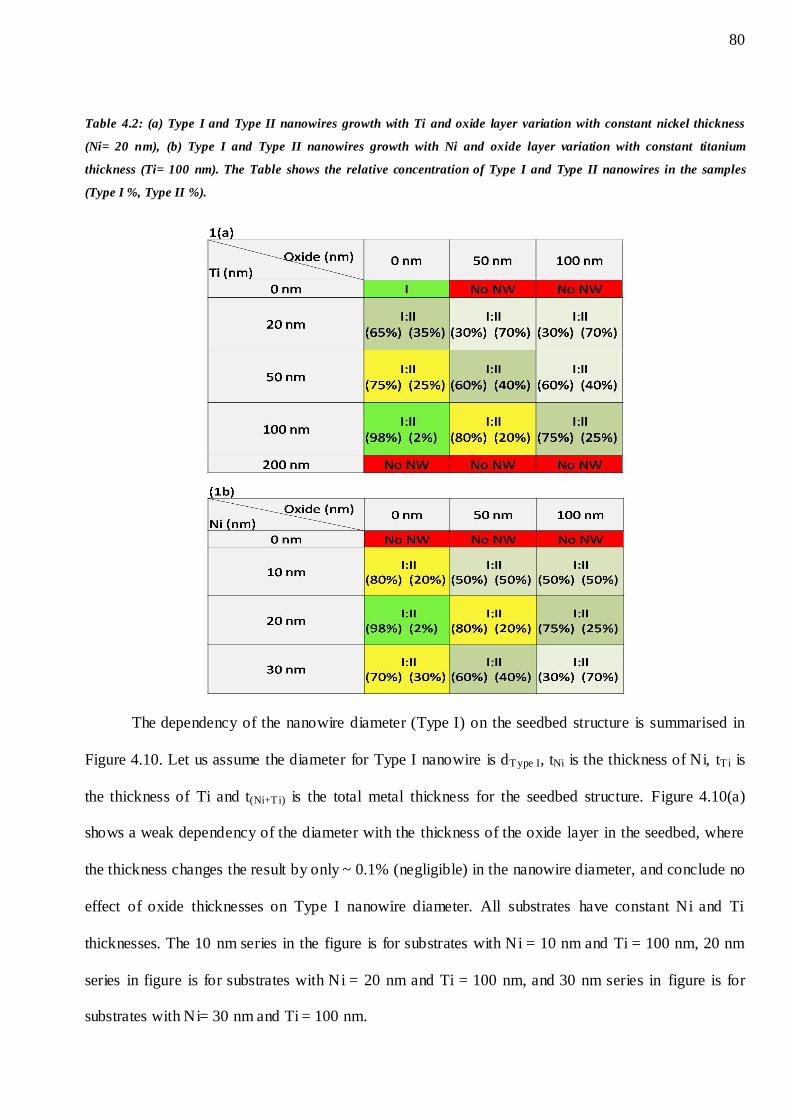
80
Table 4.2: (a) Type I and Type II nanowires growth with Ti and oxide layer variation with constant nickel thickness
(Ni= 20 nm), (b) Type I and Type II nanowires growth with Ni and oxide layer variation with constant titanium
thickness (Ti= 100 nm). The Table shows the relative concentration of Type I and Type II nanowires in the samples
(Type I %, Type II %).
The dependency of the nanowire diameter (Type I) on the seedbed structure is summarised in
Figure 4.10. Let us assume the diameter for Type I nanowire is dType I, tNi is the thickness of Ni, tTi is
the thickness of Ti and t(Ni+Ti) is the total metal thickness for the seedbed structure. Figure 4.10(a)
shows a weak dependency of the diameter with the thickness of the oxide layer in the seedbed, where
the thickness changes the result by only ~ 0.1% (negligible) in the nanowire diameter, and conclude no
effect of oxide thicknesses on Type I nanowire diameter. All substrates have constant Ni and Ti
thicknesses. The 10 nm series in the figure is for substrates with Ni = 10 nm and Ti = 100 nm, 20 nm
series in figure is for substrates with Ni = 20 nm and Ti = 100 nm, and 30 nm series in figure is for
substrates with Ni= 30 nm and Ti = 100 nm.
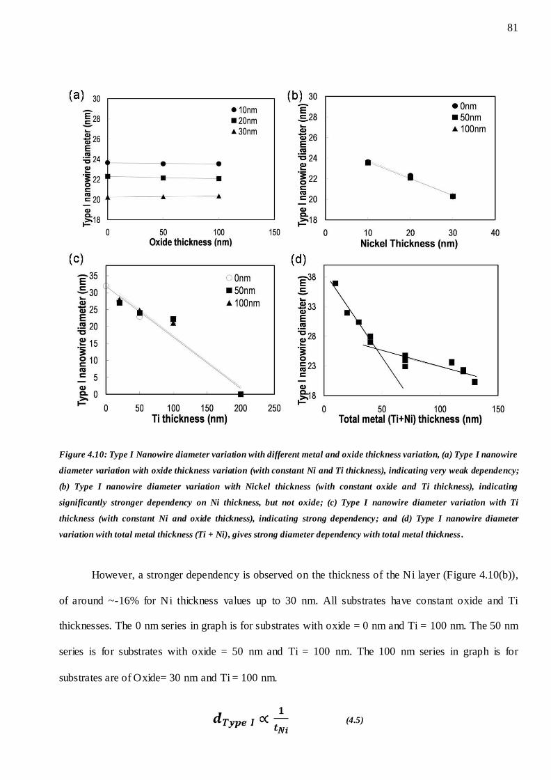
81
Figure 4.10: Type I Nanowire diameter variation with different metal and oxide thickness variation, (a) Type I nanowire
diameter variation with oxide thickness variation (with constant Ni and Ti thickness), indicating very weak dependency;
(b) Type I nanowire diameter variation with Nickel thickness (with constant oxide and Ti thickness), indicating
significantly stronger dependency on Ni thickness, but not oxide; (c) Type I nanowire diameter variation with Ti
thickness (with constant Ni and oxide thickness), indicating strong dependency; and (d) Type I nanowire diameter
variation with total metal thickness (Ti + Ni), gives strong diameter dependency with total metal thickness .
However, a stronger dependency is observed on the thickness of the Ni layer (Figure 4.10(b)),
of around ~-16% for Ni thickness values up to 30 nm. All substrates have constant oxide and Ti
thicknesses. The 0 nm series in graph is for substrates with oxide = 0 nm and Ti = 100 nm. The 50 nm
series is for substrates with oxide = 50 nm and Ti = 100 nm. The 100 nm series in graph is for
substrates are of Oxide= 30 nm and Ti = 100 nm.
(4.5)
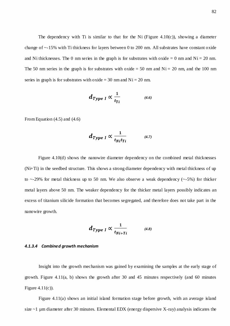
82
The dependency with Ti is similar to that for the Ni (Figure 4.10(c)), showing a diameter
change of ~-15% with Ti thickness for layers between 0 to 200 nm. All substrates have constant oxide
and Ni thicknesses. The 0 nm series in the graph is for substrates with oxide = 0 nm and Ni = 20 nm.
The 50 nm series in the graph is for substrates with oxide = 50 nm and Ni = 20 nm, and the 100 nm
series in graph is for substrates with oxide = 30 nm and Ni = 20 nm.
(4.6)
From Equation (4.5) and (4.6)
(4.7)
Figure 4.10(d) shows the nanowire diameter dependency on the combined metal thicknesses
(Ni+Ti) in the seedbed structure. This shows a strong diameter dependency with metal thickness of up
to ~-29% for metal thickness up to 50 nm. We also observe a weak dependency (~-5%) for thicker
metal layers above 50 nm. The weaker dependency for the thicker metal layers possibly indicates an
excess of titanium silicide formation that becomes segregated, and therefore does not take part in the
nanowire growth.
(4.8)
4.1.3.4 Combined growth mechanism
Insight into the growth mechanism was gained by examining the samples at the early stage of
growth. Figure 4.11(a, b) shows the growth after 30 and 45 minutes respectively (and 60 minutes
Figure 4.11(c)).
Figure 4.11(a) shows an initial island formation stage before growth, with an average island
size ~1 µm diameter after 30 minutes. Elemental EDX (energy dispersive X-ray) analysis indicates the
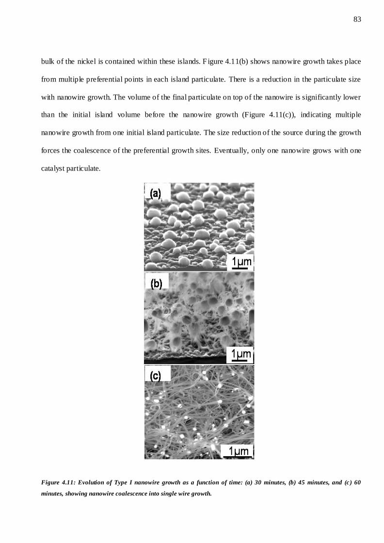
83
bulk of the nickel is contained within these islands. F igure 4.11(b) shows nanowire growth takes place
from multiple preferential points in each island particulate. There is a reduction in the particulate size
with nanowire growth. The volume of the final particulate on top of the nanowire is significantly lower
than the initial island volume before the nanowire growth (Figure 4.11(c)), indicating multiple
nanowire growth from one initial island particulate. The size reduction of the source during the growth
forces the coalescence of the preferential growth sites. Eventually, only one nanowire grows with one
catalyst particulate.
Figure 4.11: Evolution of Type I nanowire growth as a function of time: (a) 30 minutes, (b) 45 minutes, and (c) 60
minutes, showing nanowire coalescence into single wire growth.
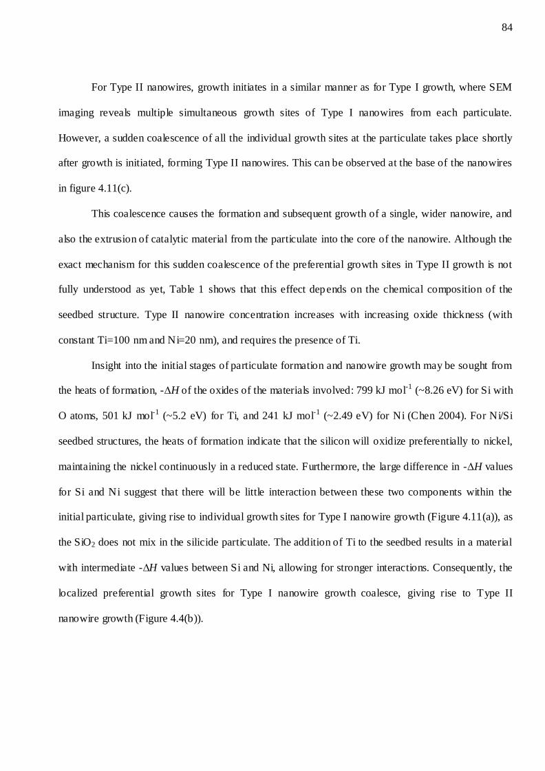
84
For Type II nanowires, growth initiates in a similar manner as for Type I growth, where SEM
imaging reveals multiple simultaneous growth sites of Type I nanowires from each particulate.
However, a sudden coalescence of all the individual growth sites at the particulate takes place shortly
after growth is initiated, forming Type II nanowires. This can be observed at the base of the nanowires
in figure 4.11(c).
This coalescence causes the formation and subsequent growth of a single, wider nanowire, and
also the extrusion of catalytic material from the particulate into the core of the nanowire. Although the
exact mechanism for this sudden coalescence of the preferential growth sites in Type II growth is not
fully understood as yet, Table 1 shows that this effect depends on the chemical composition of the
seedbed structure. Type II nanowire concentration increases with increasing oxide thickness (with
constant Ti=100 nm and Ni=20 nm), and requires the presence of Ti.
Insight into the initial stages of particulate formation and nanowire growth may be sought from
the heats of formation, -∆H of the oxides of the materials involved: 799 kJ mol-1 (~8.26 eV) for Si with
O atoms, 501 kJ mol-1 (~5.2 eV) for Ti, and 241 kJ mol-1 (~2.49 eV) for Ni (Chen 2004). For Ni/Si
seedbed structures, the heats of formation indicate that the silicon will oxidize preferentially to nickel,
maintaining the nickel continuously in a reduced state. Furthermore, the large difference in -∆H values
for Si and Ni suggest that there will be little interaction between these two components within the
initial particulate, giving rise to individual growth sites for Type I nanowire growth (Figure 4.11(a)), as
the SiO2 does not mix in the silicide particulate. The addition of Ti to the seedbed results in a material
with intermediate -∆H values between Si and Ni, allowing for stronger interactions. Consequently, the
localized preferential growth sites for Type I nanowire growth coalesce, giving rise to Type II
nanowire growth (Figure 4.4(b)).
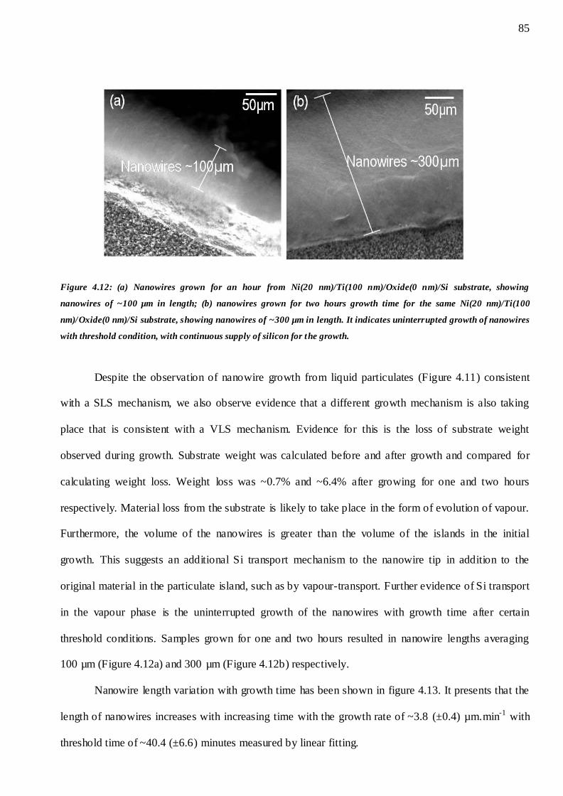
85
Figure 4.12: (a) Nanowires grown for an hour from Ni(20 nm)/Ti(100 nm)/Oxide(0 nm)/Si substrate, showing
nanowires of ~100 µm in length; (b) nanowires grown for two hours growth time for the same Ni(20 nm)/Ti(100
nm)/Oxide(0 nm)/Si substrate, showing nanowires of ~300 µm in length. It indicates uninterrupted growth of nanowires
with threshold condition, with continuous supply of silicon for the growth.
Despite the observation of nanowire growth from liquid particulates (Figure 4.11) consistent
with a SLS mechanism, we also observe evidence that a different growth mechanism is also taking
place that is consistent with a VLS mechanism. Evidence for this is the loss of substrate weight
observed during growth. Substrate weight was calculated before and after growth and compared for
calculating weight loss. Weight loss was ~0.7% and ~6.4% after growing for one and two hours
respectively. Material loss from the substrate is likely to take place in the form of evolution of vapour.
Furthermore, the volume of the nanowires is greater than the volume of the islands in the initial
growth. This suggests an additional Si transport mechanism to the nanowire tip in addition to the
original material in the particulate island, such as by vapour-transport. Further evidence of Si transport
in the vapour phase is the uninterrupted growth of the nanowires with growth time after certain
threshold conditions. Samples grown for one and two hours resulted in nanowire lengths averaging
100 µm (Figure 4.12a) and 300 µm (Figure 4.12b) respectively.
Nanowire length variation with growth time has been shown in figure 4.13. It presents that the
length of nanowires increases with increasing time with the growth rate of ~3.8 (±0.4) µm.min-1 with
threshold time of ~40.4 (±6.6) minutes measured by linear fitting.
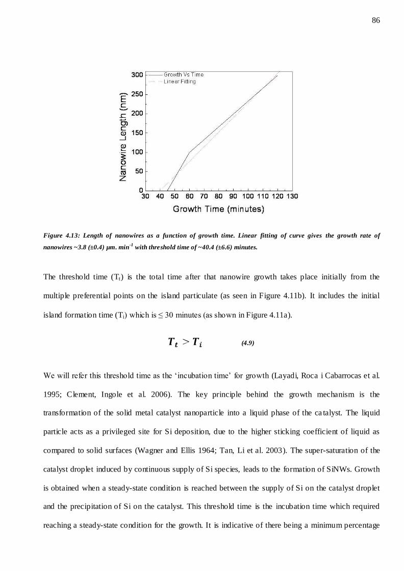
86
Figure 4.13: Length of nanowires as a function of growth time. Linear fitting of curve gives the growth rate of
nanowires ~3.8 (±0.4) µm. min-1
with threshold time of ~40.4 (±6.6) minutes.
The threshold time (Tt) is the total time after that nanowire growth takes place initially from the
multiple preferential points on the island particulate (as seen in Figure 4.11b). It includes the initial
island formation time (Ti) which is ≤ 30 minutes (as shown in Figure 4.11a).
(4.9)
We will refer this threshold time as the ‗incubation time‘ for growth (Layadi, Roca i Cabarrocas et al.
1995; Clement, Ingole et al. 2006). The key principle behind the growth mechanism is the
transformation of the solid metal catalyst nanoparticle into a liquid phase of the ca talyst. The liquid
particle acts as a privileged site for Si deposition, due to the higher sticking coefficient of liquid as
compared to solid surfaces (Wagner and Ellis 1964; Tan, Li et al. 2003). The super-saturation of the
catalyst droplet induced by continuous supply of Si species, leads to the formation of SiNWs. Growth
is obtained when a steady-state condition is reached between the supply of Si on the catalyst droplet
and the precipitation of Si on the catalyst. This threshold time is the incubation time which required
reaching a steady-state condition for the growth. It is indicative of there being a minimum percentage
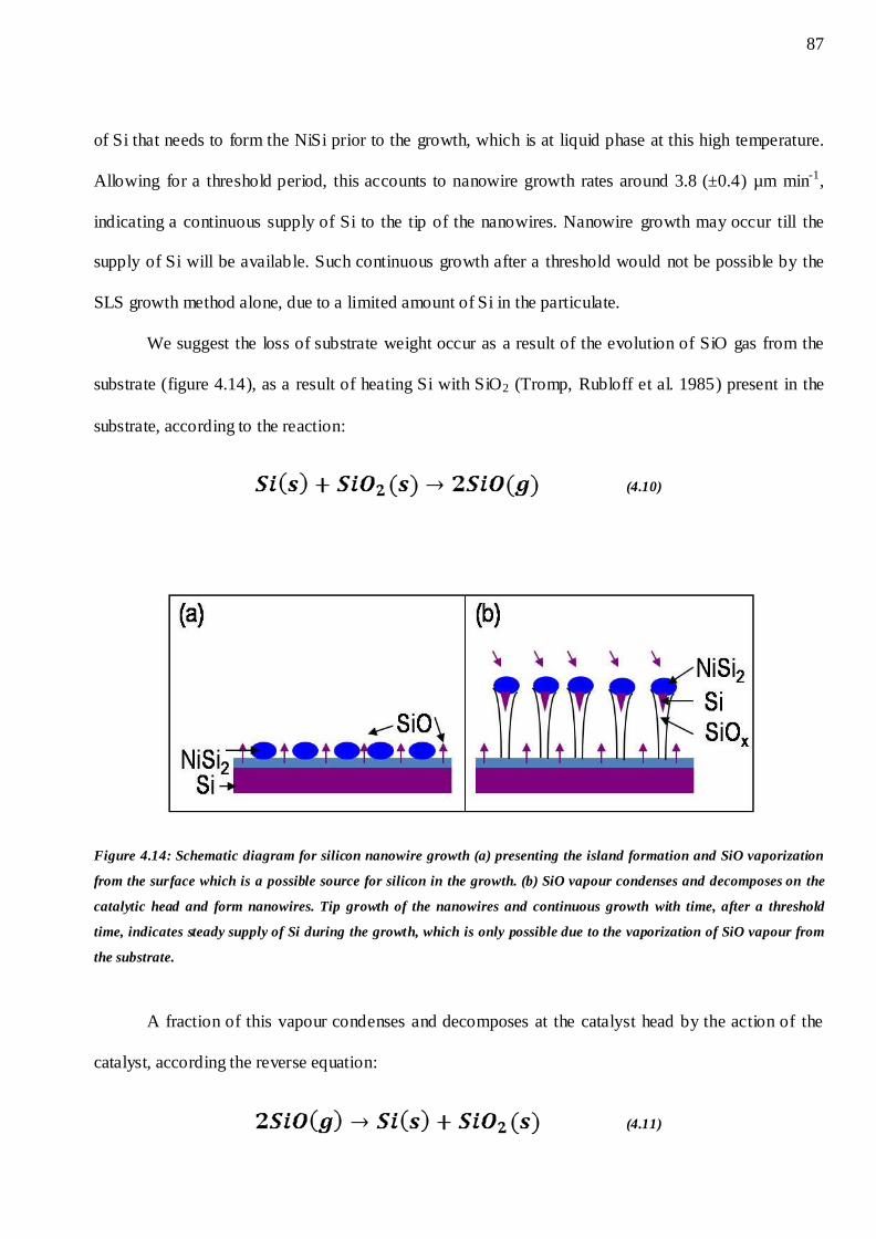
87
of Si that needs to form the NiSi prior to the growth, which is at liquid phase at this high temperature.
Allowing for a threshold period, this accounts to nanowire growth rates around 3.8 (±0.4) µm min-1,
indicating a continuous supply of Si to the tip of the nanowires. Nanowire growth may occur till the
supply of Si will be available. Such continuous growth after a threshold would not be possible by the
SLS growth method alone, due to a limited amount of Si in the particulate.
We suggest the loss of substrate weight occur as a result of the evolution of SiO gas from the
substrate (figure 4.14), as a result of heating Si with SiO2 (Tromp, Rubloff et al. 1985) present in the
substrate, according to the reaction:
(4.10)
Figure 4.14: Schematic diagram for silicon nanowire growth (a) presenting the island formation and SiO vaporization
from the surface which is a possible source for silicon in the growth. (b) SiO vapour condenses and decomposes on the
catalytic head and form nanowires. Tip growth of the nanowires and continuous growth with time, after a threshold
time, indicates steady supply of Si during the growth, which is only possible due to the vaporization of SiO vapour from
the substrate.
A fraction of this vapour condenses and decomposes at the catalyst head by the action of the
catalyst, according the reverse equation:
(4.11)
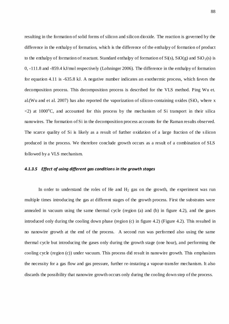
88
resulting in the formation of solid forms of silicon and silicon dioxide. The reaction is governed by the
difference in the enthalpy of formation, which is the difference of the enthalpy of formation of product
to the enthalpy of formation of reactant. Standard enthalpy of formation of Si(s), SiO(g) and SiO 2(s) is
0, -111.8 and -859.4 kJ/mol respectively (Lohninger 2006). The difference in the enthalpy of formation
for equation 4.11 is -635.8 kJ. A negative number indicates an exothermic process, which favors the
decomposition process. This decomposition process is described for the VLS method. Ping Wu et.
al.(Wu and et al. 2007) has also reported the vaporization of silicon-containing oxides (SiOx where x
<2) at 1000oC, and accounted for this process by the mechanism of Si transport in their silica
nanowires. The formation of Si in the decomposition process accounts for the Raman results observed.
The scarce quality of Si is likely as a result of further oxidation of a large fraction of the s ilicon
produced in the process. We therefore conclude growth occurs as a result of a combination of SLS
followed by a VLS mechanism.
4.1.3.5 Effect of using different gas conditions in the growth stages
In order to understand the roles of He and H2 gas on the growth, the experiment was run
multiple times introducing the gas at different stages of the growth process. First the substrates were
annealed in vacuum using the same thermal cycle (region (a) and (b) in figure 4.2), and the gases
introduced only during the cooling down phase (region (c) in figure 4.2) (Figure 4.2). This resulted in
no nanowire growth at the end of the process. A second run was performed also using the same
thermal cycle but introducing the gases only during the growth stage (one hour), and performing the
cooling cycle (region (c)) under vacuum. This process did result in nanowire growth. This emphasizes
the necessity for a gas flow and gas pressure, further re-instating a vapour-transfer mechanism. It also
discards the possibility that nanowire growth occurs only during the cooling down step of the process.
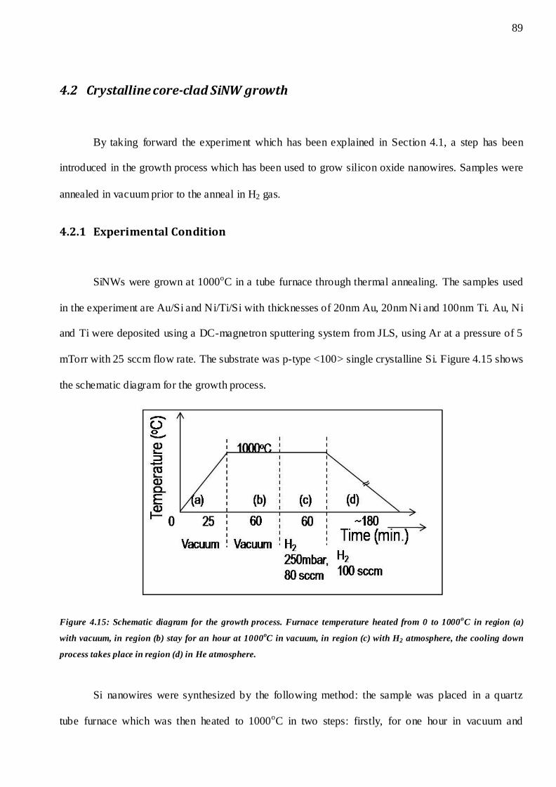
89
4.2 Crystalline core-clad SiNW growth
By taking forward the experiment which has been explained in Section 4.1, a step has been
introduced in the growth process which has been used to grow silicon oxide nanowires. Samples were
annealed in vacuum prior to the anneal in H2 gas.
4.2.1 Experimental Condition
SiNWs were grown at 1000oC in a tube furnace through thermal annealing. The samples used
in the experiment are Au/Si and Ni/Ti/Si with thicknesses of 20nm Au, 20nm Ni and 100nm Ti. Au, Ni
and Ti were deposited using a DC-magnetron sputtering system from JLS, using Ar at a pressure of 5
mTorr with 25 sccm flow rate. The substrate was p-type <100> single crystalline Si. Figure 4.15 shows
the schematic diagram for the growth process.
Figure 4.15: Schematic diagram for the growth process. Furnace temperature heated from 0 to 1000oC in region (a)
with vacuum, in region (b) stay for an hour at 1000oC in vacuum, in region (c) with H2 atmosphere, the cooling down
process takes place in region (d) in He atmosphere.
Si nanowires were synthesized by the following method: the sample was placed in a quartz
tube furnace which was then heated to 1000oC in two steps: firstly, for one hour in vacuum and
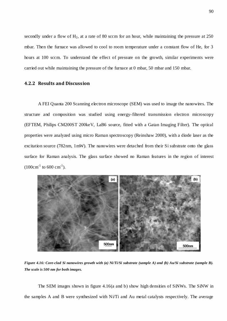
90
secondly under a flow of H2, at a rate of 80 sccm for an hour, while maintaining the pressure at 250
mbar. Then the furnace was allowed to cool to room temperature under a constant flow of He, for 3
hours at 100 sccm. To understand the effect of pressure on the growth, similar experiments were
carried out while maintaining the pressure of the furnace at 0 mbar, 50 mbar and 150 mbar.
4.2.2 Results and Discussion
A FEI Quanta 200 Scanning electron microscope (SEM) was used to image the nanowires. The
structure and composition was studied using energy-filtered transmission electron microscopy
(EFTEM, Philips CM200ST 200keV, LaB6 source, fitted with a Gatan Imaging Filter). The optical
properties were analyzed using micro Raman spectroscopy (Reinshaw 2000), with a diode laser as the
excitation source (782nm, 1mW). The nanowires were detached from their Si substrate onto the glass
surface for Raman analysis. The glass surface showed no Raman features in the region of interest
(100cm-1 to 600 cm-1).
Figure 4.16: Core-clad Si nanowires growth with (a) Ni/Ti/Si substrate (sample A) and (b) Au/Si substrate (sample B).
The scale is 500 nm for both images.
The SEM images shown in figure 4.16(a and b) show high densities of SiNWs. The SiNW in
the samples A and B were synthesized with Ni/Ti and Au metal catalysts respectively. The average
91
core-diameters for the two samples are similar, of the order of 10 nm. However, the nanowires grow to
lengths of about ~ 1 µm in sample Au (figure 4.16b) and significantly longer, of up to tens of µm in
sample Ni/Ti (figure 4.16a); the actual length was difficult to measure due to entanglement of the
nanowires.
The elemental distribution within the SiNWs in sample A and sample B was mapped using
EFTEM. High resolution imaging and diffractograms show that the grown nanowires have core-clad
structures, with a crystalline core cladded by an amorphous coating. Figure 4.17(a) shows the
elemental distribution for SiNWs grown on sample A, revealing a Ni and Si mix at the catalyst tip,
most likely as a silicide. SiNWs in sample A have a crystalline Si core covered with a n amorphous
oxide clad (figure 4.17b). The oxide clad is much thicker than the native oxide thickness (~2-5 nm)
which forms by oxidation of silicon nanowires in ambient air, as is the case where nanowires are
grown with silane via CVD. The average diameter (15.5 nm) of the crystalline core is determined from
the HRTEM micrographs of 100 SiNWs in sample A.
Figure 4.17: EFTEM analysis of SiNWs; (a) SiNW with Ni/Ti/Si substrate (sample A); Si (green), Oxygen (blue) and Ni
(orange). (b) SiNWs grown on Ni/Ti/Si substrate (sample A); 12 nm core diameter and 12 nm oxide clad thickness and;
(c) Au/Si substrate (sample B) ; 10 nm core diameter and 15 nm oxide clad thickness.
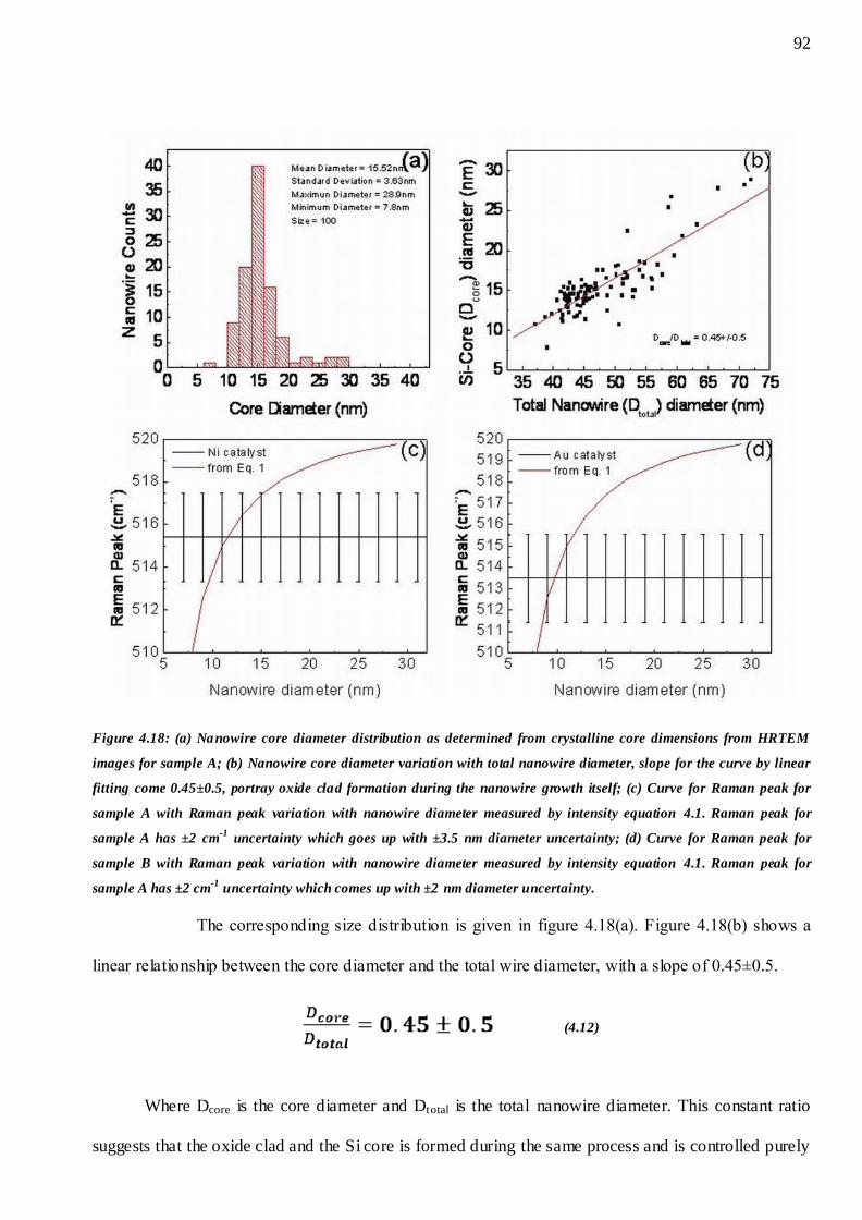
92
Figure 4.18: (a) Nanowire core diameter distribution as determined from crystalline core dimensions from HRTEM
images for sample A; (b) Nanowire core diameter variation with total nanowire diameter, slope for the curve by linear
fitting come 0.45±0.5, portray oxide clad formation during the nanowire growth itself; (c) Curve for Raman peak for
sample A with Raman peak variation with nanowire diameter measured by intensity equation 4.1. Raman peak for
sample A has ±2 cm-1
uncertainty which goes up with ±3.5 nm diameter uncertainty; (d) Curve for Raman peak for
sample B with Raman peak variation with nanowire diameter measured by intensity equation 4.1. Raman peak for
sample A has ±2 cm-1
uncertainty which comes up with ±2 nm diameter uncertainty.
The corresponding size distribution is given in figure 4.18(a). Figure 4.18(b) shows a
linear relationship between the core diameter and the total wire diameter, with a slope of 0.45±0.5.
(4.12)
Where Dcore is the core diameter and Dtotal is the total nanowire diameter. This constant ratio
suggests that the oxide clad and the Si core is formed during the same process and is controlled purely
93
through the catalyst size (figure 4.17c). The presence of the catalyst particle on the tip and the constant
diameter of the wires indicate that these nanowires grow via a VLS mechanism, where a steady state
between Si arriving at the catalyst and Si being extruded from the catalyst is achieved. The straight line
fit in Figure 4.18b also shows that no nanowires can be obtained below 24.5 nm which is the total
nanowire diameter including core and clad. This can be interpreted as the critical catalyst size below
which it is not forming a nanowire. The critical catalyst size manifests the thermodynamic limit for the
minimum radius of the catalyst droplets.
PL measurements were obtained at room temperature using the 281 nm excitation wavelength
in a Cary Eclipse Varian Fluorescence Spectroscope. Figure 4.19 shows that the PL spectra (a)
obtained for SiNWs for Ni/Ti/Si seedbed substrate and spectra (b) for SiNWs for Au/Si seedbed
structure. Spectra (a) is centered at ~622 nm and at spectra (b) is centered at ~618 nm.
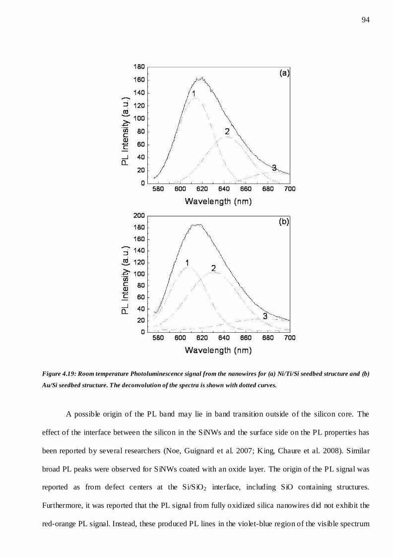
94
Figure 4.19: Room temperature Photoluminescence signal from the nanowires for (a) Ni/Ti/Si seedbed structure and (b)
Au/Si seedbed structure. The deconvolution of the spectra is shown with dotted curves.
A possible origin of the PL band may lie in band transition outside of the silicon core. The
effect of the interface between the silicon in the SiNWs and the surface side on the PL properties has
been reported by several researchers (Noe, Guignard et al. 2007; King, Chaure et al. 2008). Similar
broad PL peaks were observed for SiNWs coated with an oxide layer. The origin of the PL signal was
reported as from defect centers at the Si/SiO2 interface, including SiO containing structures.
Furthermore, it was reported that the PL signal from fully oxidized silica nanowires did not exhibit the
red-orange PL signal. Instead, these produced PL lines in the violet-blue region of the visible spectrum
95
(410-450 nm) (Kar and Chaudhuri 2005). No emission centers were observed between 500-700 nm for
the fully oxidized silica nanowires.
Assuming the shape of the bands to be Gaussian, a multi-Gaussian deconvolution has been
done for both PL spectra. Three elementary bands 1, 2 and 3 with maxima at 613, 642 and 685 nm
respectively for Ni/Ti/Si seedbed structure and with maxima at 607, 630 and 676 nm respectively for
Au/Si seedbed structure are required to produce the composite curve (as shown in Figure 4.19 (a and
b)) that closely fits the experimental data. Silicon is an indirect band-gap semiconductor with small
band-gap (~1.1 eV). Big changes in the band structure takes place as size decreases, causing a
transformation from indirect to direct band gap structure and/or an increase in the band-gap. The blue
shift and increase of intensity in the PL spectra is attributed due to decrease in silicon size (Feng, Yu et
al. 1999). Salhi, Gelloz et al. (2007) have shown the increase in PL peak intensity with decrease in the
crystalline core SiNW size. The indirect-to-direct transition in the band gap may not occur for SiNWs
with large diameter and this would result in weak PL. Quantum confinement in Si crystallites is
probably responsible for the peak 3. Small intensity of peak 3 may be attrib uted due to the large
diameter compare to the dimensions of the free exciton (the Bohr radius of about 5 nm) of bulk silicon.
SiNWs grown with both seedbed substrates have oxide clad. Oxide clad has a direct band gap, this
surface layer itself does not contribute to the visible PL spectrum because the band gap energy is out of
the visible range (>155 nm). However, the oxide clad layer plays a role in the PL spectra of nanowires.
It is responsible for the reduction of the number of surface dangling bonds that act as non-radiative
recombination centers of the crystalline nanowire core. The oxide clad induces the quantum
confinement of photo-generated carriers within the crystalline Si core which is responsible for the PL
peak. Also it creates a novel electronic state in the interfacial region due to the oxygen atoms
interconnecting the crystalline SiNW core with a SiO2 layer. Peak 1 and peak 2 can be attributed to the
Si/SiO2 interface and SiO2 layer. Intensity of spectra (b) is large compare to spectra (a). It is due to the
more intense peak 2 in spectra (b) compared to spectra (a). Higher intensity is attributed to the greater
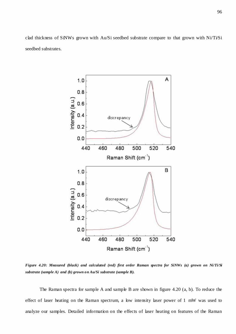
96
clad thickness of SiNWs grown with Au/Si seedbed substrate compare to that grown with Ni/Ti/Si
seedbed substrates.
Figure 4.20: Measured (black) and calculated (red) first order Raman spectra for SiNWs (a) grown on Ni/Ti/Si
substrate (sample A) and (b) grown on Au/Si substrate (sample B).
The Raman spectra for sample A and sample B are shown in figure 4.20 (a, b). To reduce the
effect of laser heating on the Raman spectrum, a low intensity laser power of 1 mW was used to
analyze our samples. Detailed information on the effects of laser heating on features of the Raman
97
spectra of Si nanowires have been discussed in Section 4.1.3. We will concentrate on the changes in
the first-order optical mode, when compared to standard c-Si. A Raman peak at 521.1 cm-1, with the
full-width-at-half-maximum of 4.1 cm-1 was observed for c-Si. This is due to the scattering of the first-
order TO optical phonons of c-Si. The Raman spectra of samples A and B (figure 4.20 a, b) show
prominent Raman features at ~515.4 and ~513.4 cm-1, respectively, with a shoulder at 495.2 and 490.6
cm-1, respectively. When comparing them with the c-Si Raman spectrum, SiNWs on samples A and B
show a similar band, exhibiting broader widths and a red shift in the peak positions. Note that the
nanowires no longer lie on the crystalline silicon substrate, but have been transferred onto glass. This
feature has also been observed by other research groups for crystalline silicon nanowires (Pan and et
al. 2005; Chen, Peng et al. 2007). The observed line width broadening can be explained with the
breakdown of the phonon momentum selection rule q≈0, specific of the Raman scattering in ordered
systems. In the case of crystals of very small size, this rule is no longer valid as the phonons are
confined in space and all the phonons over the Brillouin zone will contribute to the first order Raman
spectra. The weight of the off-center phonon increases as the crystal size decreases and the phonon
dispersion causes an asymmetrical broadening and the shift of the Raman peaks (Campbell and
Fauchet 1986; Bersani, Lottici et al. 1998).
Table 4.3: The Raman frequency, frequency shi ft from the Raman frequency of c-Si, The FWHM, the coefficient of
broadening (Cb) defined by FWHMSiNWs/FWHMc-Si, the asymmetric coefficient (Ca) defined by LWHM/RWHM (the
left width at half maximum (LWHM) and the right width at half maximum (RWHM) from the central peak position),
the diameter of the nanowires measured by TEM image and the diameter of the nanowires measured by Raman spectra.
98
Spectral parameters of the first-order optical phonon spectra of SiNWs (sample A and B) and
of c-Si are listed in Table 4.3. The spectral parameters are the Raman frequency, the frequency shift,
the coefficient of broadening (Cb) defined by FWHMSiNWs/FWHMc-Si, and the asymmetric coefficient
(Ca) defined by LWHM/RWHM, where LWHM and RWHM are the left-width-at-half-maximum and
right-width-at-half-maximum from the central peak position respectively. From Table 4.3, we found
that the frequency shift, FWHM, the coefficient of broadening Cb, and the asymmetric coefficient Ca of
sample B are all larger than those of sample A. This is expected qualitatively from the values in the
order of size measured by TEM listed in Table 4.3, giving further support to that the Raman spectra
shown in figure 4.20 (a, b) resulting from the quantum confinement effect of the SiNW for samples A
and B. The phonon confinement model has been explained in Section 4.2. The Raman intensity
function (Equation 4.1) was fitted to our experimental data and the comparison between the
experiment and the simulation based on the phonon confinement model is shown in figure 4.20 (a, b)
for samples A and B respectively. The Raman peak variation with nanowire diameter has be en shown
in figure 4.18(c, d), measured by equation 4.1 with different L values. Straight line at 515.4 cm-1 and
513.4 cm-1 in figure 4.18c and figure 4.18d is the Raman peak for SiNWs grown with Ni and Au
catalysts respectively. Error bars of ±2 cm-1 are shown in curves for both SiNW peaks. Nanowire
diameters for sample A and sample B by Raman fitting provides 11.5±3.5 nm and 9.5±2 nm, as their
diameters as listed in Table 4.3. There is good general agreement in spectral features between
experimental and calculated Raman spectra, indicating that the identification of the Raman peak at
~513.4 and ~515.4 cm-1 in figures 4.18a and 4.18b is correct.
On closer examination, some discrepancies have been observed between the experimental and
the calculated spectra. The calculated spectra do not explain the features on the low frequency sides
with shoulders at ~490.6 cm-1 for sample A and ~495.2 cm-1 for sample B, suggesting that there are
other components not due to the SiNWs. They may be attributed (Veprek, Sarott et al. 1987) to the
oxide that covers the SiNWs, which has a Raman structure between 400 cm-1 and 550 cm-1, with a
peak at ~490 cm-1.
99
Growth conditions have been investigated with more experiments. Critical growth temperatures
were examined by varying the growth temperature. No growth was observed at 950oC, indicating
1000oC is essential for the growth. To investigate the importance of gas in the growth, experiments
were carried out without any flow of gas in step two. No nanowire growth was observed on the
substrate. SiNW growth with the help of Ti and Ni seedbed structure has been explained in Section
4.1. Growth mechanisms were described with SLS and VLS. In the SLS mechanism, growth
temperatures for nanowires depend on the eutectic temperature of the metal silicide, in the present
case, no growth was observed at 950oC with Au catalyst. It should be noted that 950oC is much higher
than the eutectic temperature of Au-Si (360oC), indicating the likelihood of another growth
mechanism. We suggest a combination of SLS and VLS mechanism to explain the growth in our
system. In an initial stage of the SLS growth mechanism start process, nickel (or Au in sample B)
silicide islands form. SiO vapour evaporates from the substrate as a result of heating the Si at 1000oC
(Tromp, Rubloff et al. 1985) according to the reaction:
(4.13)
SiO vapor sticks to the catalyst head and condenses and decomposes at the catalyst head by the
action of the catalyst according to the reverse equation:
(4.14)
resulting in the formation of solid forms of silicon and silicon oxide. The temperature is high
enough for the decomposition of SiO vapor. After decomposition, the silicon is absorbed into the
catalyst island, while oxide remains at the surface of the island. Then SiNWs grow according to the
VLS mechanism.
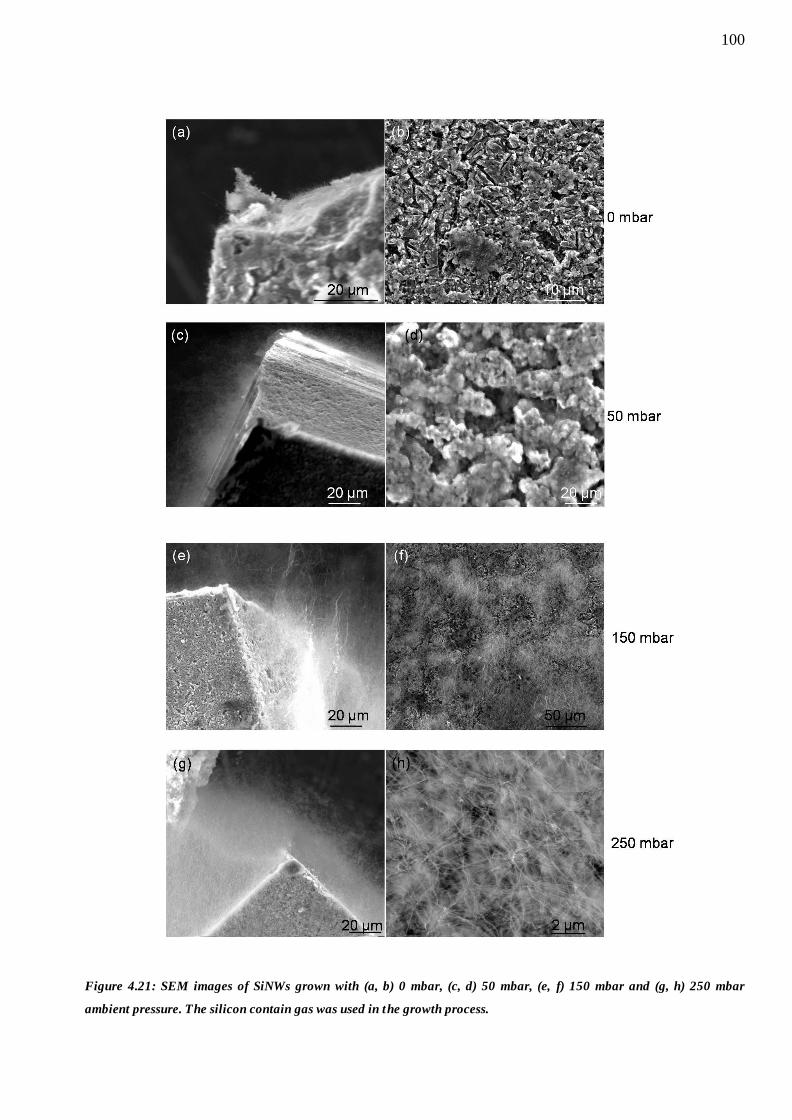
100
Figure 4.21: SEM images of SiNWs grown with (a, b) 0 mbar, (c, d) 50 mbar, (e, f) 150 mbar and (g, h) 250 mbar
ambient pressure. The silicon contain gas was used in the growth process.
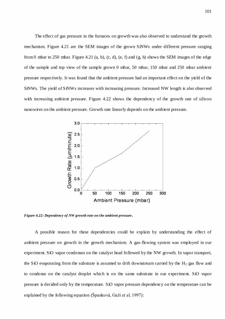
101
The effect of gas pressure in the furnaces on growth was also observed to understand the growth
mechanism. Figure 4.21 are the SEM images of the grown SiNWs under different pressure ranging
from 0 mbar to 250 mbar. Figure 4.21 (a, b), (c, d), (e, f) and (g, h) shows the SEM images of the edge
of the sample and top view of the sample grown 0 mbar, 50 mbar, 150 mbar and 250 mbar ambient
pressure respectively. It was found that the ambient pressure had an important effect on the yield of the
SiNWs. The yield of SiNWs increases with increasing pressure. Increased NW length is also observed
with increasing ambient pressure. Figure 4.22 shows the dependency of the growth rate of silicon
nanowires on the ambient pressure. Growth rate linearly depends on the ambient pressure.
Figure 4.22: Dependency of NW growth rate on the ambient pressure.
A possible reason for these dependencies could be explain by understanding the effect of
ambient pressure on growth in the growth mechanism. A gas- flowing system was employed in our
experiment. SiO vapor condenses on the catalyst head followed by the NW growth. In vapor transport,
the SiO evaporating from the substrate is assumed to drift downstream carried by the H2 gas flow and
to condense on the catalyst droplet which is on the same substrate in our experiment. SiO vapor
pressure is decided only by the temperature. SiO vapor pressure dependency on the temperature can be
explained by the following equation (Španková, Gaži et al. 1997):
102
(4.15)
where p is vapor pressure in Pa and Ts is substrate temperature in Kelvins. SiO vapor pressure
increases with increasing temperature. In our experiments, NWs have been grown at the same
temperature with different ambient pressure. Therefore as the ambient pressure increases, the SiO
vapor pressure would be constant. SiO vapor transport along the tube is due to the carrier gas flow.
Since vapor transport is diffusion driven, it can be suppressed if the total H2 gas pressure is increased.
The diffusion coefficient is inversely proportional to the total pressure (Colli and et al. 2006; Hudson
2008). With decreasing ambient pressure, diffusion will increase and the SiO vapors are swept away
by the carrier gas from the surface of the source material. Since in our mechanism, source and
deposition sites both exist on the same wafer, the SiO vapour will be swept away by the substrate and
will provide low yield of the SiNWs at low ambient pressure. High yield of SiO vapor at the catalyst
droplet at high ambient pressure is attributed to the lower diffusion coefficient. High yield will result
in high growth rate of NWs at high ambient pressure.
4.3 Silicon nanopillar fabrication through etching
Two processes have been tested to select the proper mask for etching in our experiment: (1)
Metal nanoparticle film and (2) metal island formation.
4.3.1 Mask formation
4.3.1.1 Metal nano-particle film
Nano-particles can be a good choice for making masks for etching. The diameter of nano-
pillars can be controlled by changing the nano particle diameter. As a Ni catalyst will be used for
further CNT growth, we have chosen Ni nano particles. An average diameter of ~200nm of Ni nano-
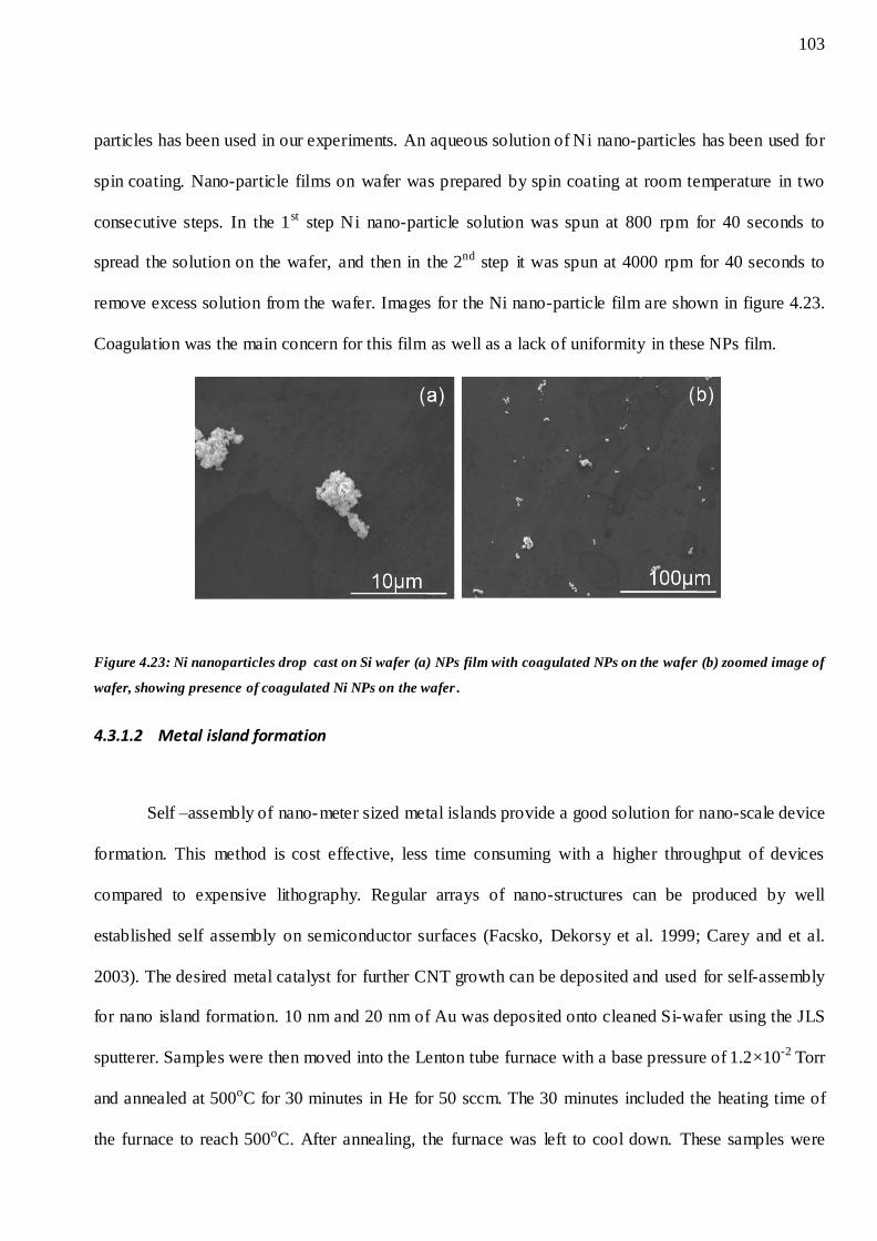
103
particles has been used in our experiments. An aqueous solution of Ni nano-particles has been used for
spin coating. Nano-particle films on wafer was prepared by spin coating at room temperature in two
consecutive steps. In the 1st step Ni nano-particle solution was spun at 800 rpm for 40 seconds to
spread the solution on the wafer, and then in the 2nd step it was spun at 4000 rpm for 40 seconds to
remove excess solution from the wafer. Images for the Ni nano-particle film are shown in figure 4.23.
Coagulation was the main concern for this film as well as a lack of uniformity in these NPs film.
Figure 4.23: Ni nanoparticles drop cast on Si wafer (a) NPs film with coagulated NPs on the wafer (b) zoomed image of
wafer, showing presence of coagulated Ni NPs on the wafer .
4.3.1.2 Metal island formation
Self –assembly of nano-meter sized metal islands provide a good solution for nano-scale device
formation. This method is cost effective, less time consuming with a higher throughput of devices
compared to expensive lithography. Regular arrays of nano-structures can be produced by well
established self assembly on semiconductor surfaces (Facsko, Dekorsy et al. 1999; Carey and et al.
2003). The desired metal catalyst for further CNT growth can be deposited and used for self-assembly
for nano island formation. 10 nm and 20 nm of Au was deposited onto cleaned Si-wafer using the JLS
sputterer. Samples were then moved into the Lenton tube furnace with a base pressure of 1.2×10⁻² Torr
and annealed at 500oC for 30 minutes in He for 50 sccm. The 30 minutes included the heating time of
the furnace to reach 500oC. After annealing, the furnace was left to cool down. These samples were
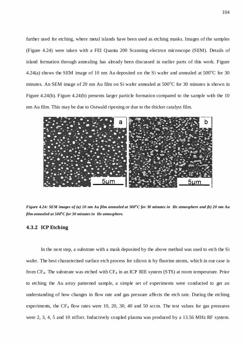
104
further used for etching, where metal islands have been used as etching masks. Images of the samples
(Figure 4.24) were taken with a FEI Quanta 200 Scanning electron microscope (SEM). Details of
island formation through annealing has already been discussed in earlier parts of this work. Figure
4.24(a) shows the SEM image of 10 nm Au deposited on the Si wafer and annealed at 500oC for 30
minutes. An SEM image of 20 nm Au film on Si wafer annealed at 500oC for 30 minutes is shown in
Figure 4.24(b). Figure 4.24(b) presents larger particle formation compared to the sample with the 10
nm Au film. This may be due to Ostwald ripening or due to the thicker catalyst film.
Figure 4.24: SEM images of (a) 10 nm Au film annealed at 500oC for 30 minutes in He atmosphere and (b) 20 nm Au
film annealed at 500oC for 30 minutes in He atmosphere.
4.3.2 ICP Etching
In the next step, a substrate with a mask deposited by the above method was used to etch the Si
wafer. The best characterised surface etch process for silicon is by fluorine atoms, which in our case is
from CF4. The substrate was etched with CF4 in an ICP RIE system (STS) at room temperature. Prior
to etching the Au array patterned sample, a simple set of experiments were conducted to get an
understanding of how changes in flow rate and gas pressure affects the etch rate. During the etching
experiments, the CF4 flow rates were 10, 20, 30, 40 and 50 sccm. The test values for gas pressures
were 2, 3, 4, 5 and 10 mTorr. Inductively coupled plasma was produced by a 13.56 MHz RF system.
105
The coil power of 600 W and platen power of 300 W was used for the experiment to create the plasma.
Samples were analyzed by taking images in a FEI Quanta 200 Scanning electron microscope (SEM).
4.3.3 Results and Discussion
The literature (van Roosmalen, Baggerman et al. 1991; Suzuki and Itabashi 1996) have already
shown that during etching, the CF4 molecules dissolved into chemically aggressive etchants such as F,
F+ and unsaturates like CF2, CF2+
through collisions in plasma.
(4.16)
The radicals and ions break the Si-Si bonding and form a layer of SiF4 in the near-surface
region which is volatile. Then the product evaporates from the surface. Simultaneously, an excess of
ions accumulates in the etched layer as free ions and strikes the surface perpendicularly, making the
etch anisotropic.
(4.17)
(4.18)
Chemical etching is the outcome of the pure chemical reaction between silicon and fluorine,
resulting in isotropic profiles. But the ion-enhanced etching takes place along the direction of incident
ions, providing the vertical etch profile. Therefore, the competence between chemical etching and ion-
enhanced etching will determined the etch anisotropy.
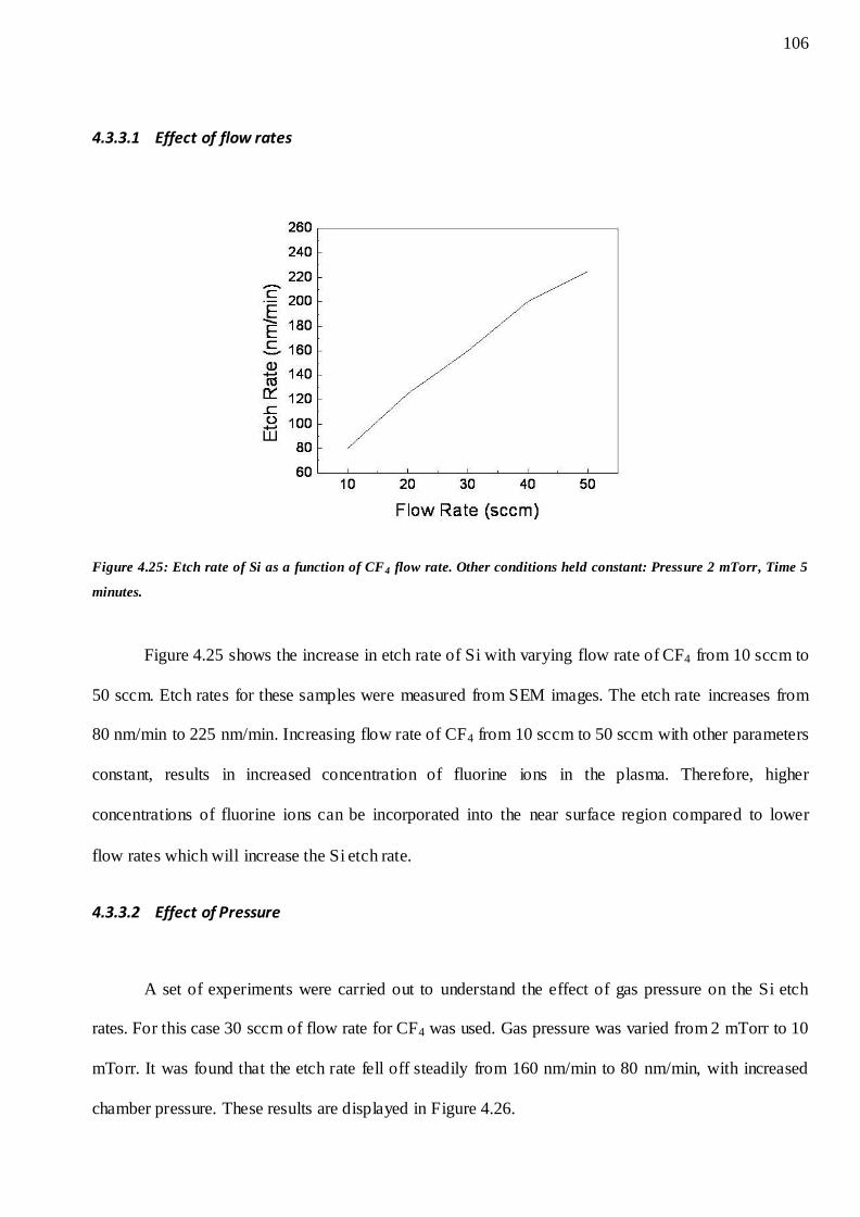
106
4.3.3.1 Effect of flow rates
Figure 4.25: Etch rate of Si as a function of CF4 flow rate. Other conditions held constant: Pressure 2 mTorr, Time 5
minutes.
Figure 4.25 shows the increase in etch rate of Si with varying flow rate of CF4 from 10 sccm to
50 sccm. Etch rates for these samples were measured from SEM images. The etch rate increases from
80 nm/min to 225 nm/min. Increasing flow rate of CF4 from 10 sccm to 50 sccm with other parameters
constant, results in increased concentration of fluorine ions in the plasma. Therefore, higher
concentrations of fluorine ions can be incorporated into the near surface region compared to lower
flow rates which will increase the Si etch rate.
4.3.3.2 Effect of Pressure
A set of experiments were carried out to understand the effect of gas pressure on the Si etch
rates. For this case 30 sccm of flow rate for CF4 was used. Gas pressure was varied from 2 mTorr to 10
mTorr. It was found that the etch rate fell off steadily from 160 nm/min to 80 nm/min, with increased
chamber pressure. These results are displayed in Figure 4.26.

107
Figure 4.26: Etch rate of Si as a function of gas pressure. Other conditions held constant: Gas flow rate 30 sccm, Time
5 minutes.
At high pressure, for a constant flow rate, the mean free path will decrease giving the increase
in particle collision rate, resulting in reduced average electron energy (Melliar—Smith and Mogab
1978). Radicals and ions will be generated at a smaller rate due to the reduction in electron energy,
which results in a decrease in etch rates with increasing pressure. In addition, the anisotropy of the
etching of Si also decreased with increased pressure. This is the result of a decrease in generation of
radicals and ions which will increase the chemical etching compare to ion-enhanced etching. It will
decrease the anisotropy of the etching.
Figure 4.27 presents the SEM image of ICP-RIE etched sample (10 nm Au deposited, annealed
at 500oC for 30 minutes in He atmosphere). The sample was etched in CF4 for 5 minutes at 2 mTorr
pressure with 30 sccm flow rate. An inductively coupled plasma was produced by a 13.56 MHz RF
system. The coil power of 600 W and platen power of 300 W was used for the experiment to create the
plasma.
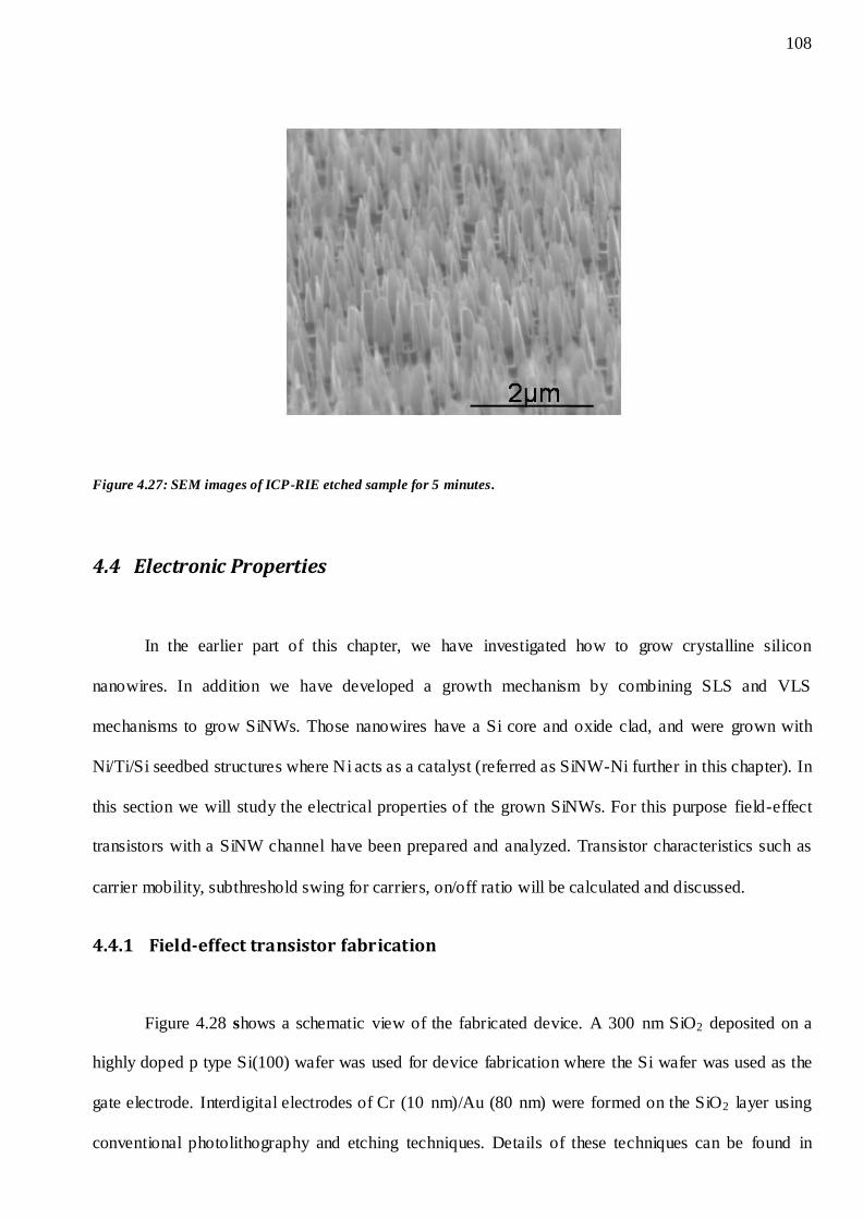
108
Figure 4.27: SEM images of ICP-RIE etched sample for 5 minutes.
4.4 Electronic Properties
In the earlier part of this chapter, we have investigated how to grow crystalline silicon
nanowires. In addition we have developed a growth mechanism by combining SLS and VLS
mechanisms to grow SiNWs. Those nanowires have a Si core and oxide clad, and were grown with
Ni/Ti/Si seedbed structures where Ni acts as a catalyst (referred as SiNW-Ni further in this chapter). In
this section we will study the electrical properties of the grown SiNWs. For this purpose field-effect
transistors with a SiNW channel have been prepared and analyzed. Transistor characteristics such as
carrier mobility, subthreshold swing for carriers, on/off ratio will be calculated and discussed.
4.4.1 Field-effect transistor fabrication
Figure 4.28 shows a schematic view of the fabricated device. A 300 nm SiO2 deposited on a
highly doped p type Si(100) wafer was used for device fabrication where the Si wafer was used as the
gate electrode. Interdigital electrodes of Cr (10 nm)/Au (80 nm) were formed on the SiO2 layer using
conventional photolithography and etching techniques. Details of these techniques can be found in
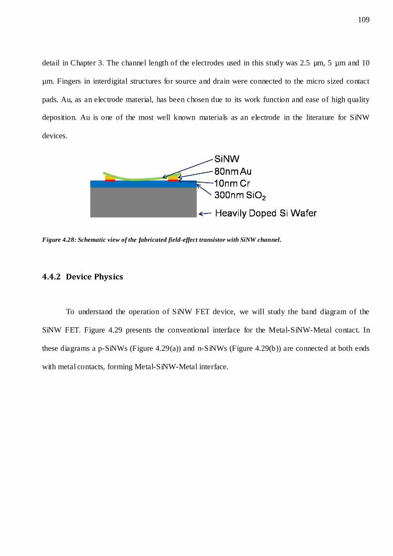
109
detail in Chapter 3. The channel length of the electrodes used in this study was 2.5 µm, 5 µm and 10
µm. Fingers in interdigital structures for source and drain were connected to the micro sized contact
pads. Au, as an electrode material, has been chosen due to its work function and ease of high quality
deposition. Au is one of the most well known materials as an electrode in the literature for SiNW
devices.
Figure 4.28: Schematic view of the fabricated field-effect transistor with SiNW channel.
4.4.2 Device Physics
To understand the operation of SiNW FET device, we will study the band diagram of the
SiNW FET. Figure 4.29 presents the conventional interface for the Metal-SiNW-Metal contact. In
these diagrams a p-SiNWs (Figure 4.29(a)) and n-SiNWs (Figure 4.29(b)) are connected at both ends
with metal contacts, forming Metal-SiNW-Metal interface.
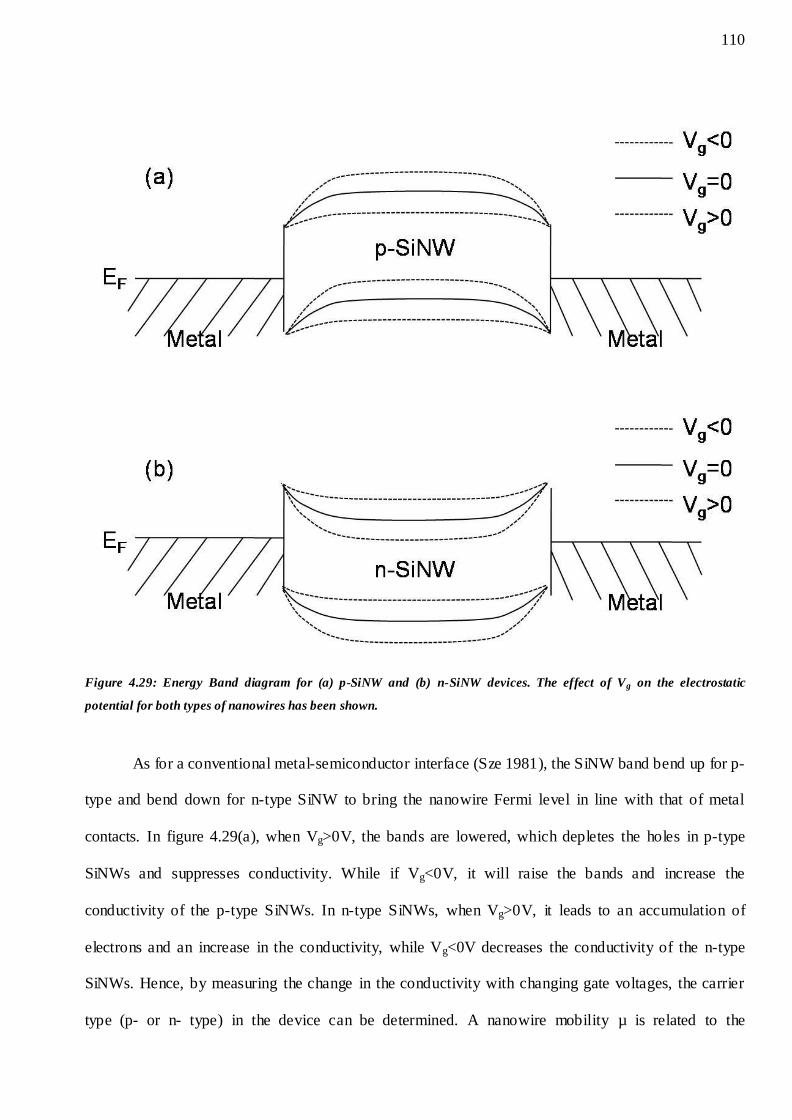
110
Figure 4.29: Energy Band diagram for (a) p-SiNW and (b) n-SiNW devices. The effect of Vg on the electrostatic
potential for both types of nanowires has been shown.
As for a conventional metal-semiconductor interface (Sze 1981), the SiNW band bend up for p-
type and bend down for n-type SiNW to bring the nanowire Fermi level in line with that of metal
contacts. In figure 4.29(a), when Vg>0V, the bands are lowered, which depletes the holes in p-type
SiNWs and suppresses conductivity. While if Vg<0V, it will raise the bands and increase the
conductivity of the p-type SiNWs. In n-type SiNWs, when Vg>0V, it leads to an accumulation of
electrons and an increase in the conductivity, while Vg<0V decreases the conductivity of the n-type
SiNWs. Hence, by measuring the change in the conductivity with changing gate voltages, the carrier
type (p- or n- type) in the device can be determined. A nanowire mobility µ is related to the
111
transconductance gm of the FETs by the following relation (Cui, Duan et al. 2000) which can be used
to calculate the carrier mobility.
(4.19)
where
(4.20)
where gm is the transconductance, L is the channel length (i.e. distance between the source and drain),
V is the source-drain voltage, for which the transfer characteristics are measured and C is the
capacitance, ε is the dielectric constant of the SiO2 layer (3.9 for SiO2 (Aissa & Khakani, 2009)), h is
the thickness of the SiO2 layer and r is the radius of the nanowires.
The transconductance gm can be obtained from the Ids vs Vgs plot by using the following
relation;
(4.21)
at a fixed V in the linear region.
4.4.3 Device Measurements
SiNW-Ni was sonicated off the substrate in IPA. The solution was then drop cast on the above
mentioned pre patterned electrode structure. The device was heated at 100oC for 10 minutes to remove
the solvent. Field-effect transistor measurements have been done to understand the electrical properties
of these nanowires.
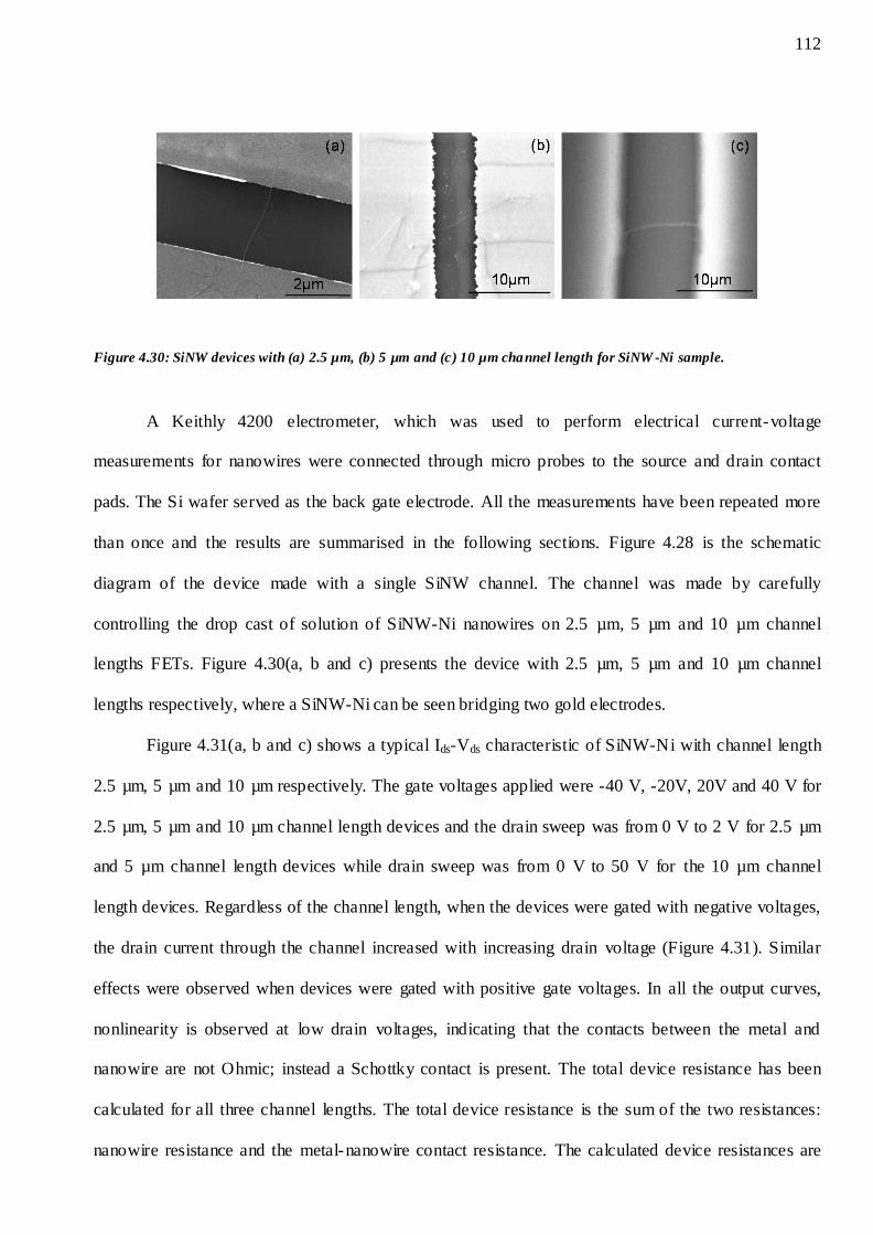
112
Figure 4.30: SiNW devices with (a) 2.5 µm, (b) 5 µm and (c) 10 µm channel length for SiNW -Ni sample.
A Keithly 4200 electrometer, which was used to perform electrical current-voltage
measurements for nanowires were connected through micro probes to the source and drain contact
pads. The Si wafer served as the back gate electrode. All the measurements have been repeated more
than once and the results are summarised in the following sections. Figure 4.28 is the schematic
diagram of the device made with a single SiNW channel. The channel was made by carefully
controlling the drop cast of solution of SiNW-Ni nanowires on 2.5 µm, 5 µm and 10 µm channel
lengths FETs. Figure 4.30(a, b and c) presents the device with 2.5 µm, 5 µm and 10 µm channel
lengths respectively, where a SiNW-Ni can be seen bridging two gold electrodes.
Figure 4.31(a, b and c) shows a typical Ids-Vds characteristic of SiNW-Ni with channel length
2.5 µm, 5 µm and 10 µm respectively. The gate voltages applied were -40 V, -20V, 20V and 40 V for
2.5 µm, 5 µm and 10 µm channel length devices and the drain sweep was from 0 V to 2 V for 2.5 µm
and 5 µm channel length devices while drain sweep was from 0 V to 50 V for the 10 µm channel
length devices. Regardless of the channel length, when the devices were gated with negative voltages,
the drain current through the channel increased with increasing drain voltage (Figure 4.31). Similar
effects were observed when devices were gated with positive gate voltages. In all the output curves,
nonlinearity is observed at low drain voltages, indicating that the contacts between the metal and
nanowire are not Ohmic; instead a Schottky contact is present. The total device resistance has been
calculated for all three channel lengths. The total device resistance is the sum of the two resistances:
nanowire resistance and the metal-nanowire contact resistance. The calculated device resistances are
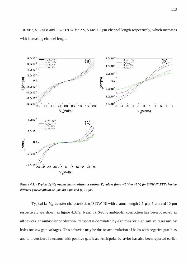
113
1.07×E7, 5.17×E8 and 1.52×E9 Ω for 2.5, 5 and 10 µm channel length respectively, which increases
with increasing channel length.
Figure 4.31: Typical Ids-Vds output characteristics at various Vg values (from -40 V to 40 V) for SiNW-Ni FETs having
different gate length (a) 2.5 µm, (b) 5 µm and (c) 10 µm.
Typical Ids-Vgs transfer characteristic of SiNW-Ni with channel length 2.5 µm, 5 µm and 10 µm
respectively are shown in figure 4.32(a, b and c). Strong ambipolar conduction has been observed in
all devices. In ambipolar conduction, transport is dominated by electrons for high gate voltages and by
holes for low gate voltages. This behavior may be due to accumulation of holes with negative gate bias
and to inversion of electrons with positive gate bias. Ambipolar behavior has also been reported earlier
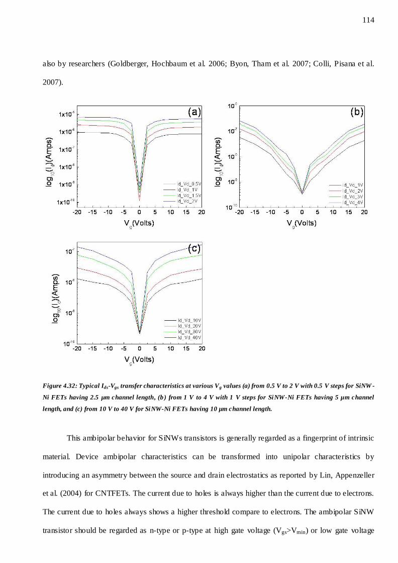
114
also by researchers (Goldberger, Hochbaum et al. 2006; Byon, Tham et al. 2007; Colli, Pisana et al.
2007).
Figure 4.32: Typical Ids-Vgs transfer characteristics at various Vg values (a) from 0.5 V to 2 V with 0.5 V steps for SiNW -
Ni FETs having 2.5 µm channel length, (b ) from 1 V to 4 V with 1 V steps for SiNW-Ni FETs having 5 µm channel
length, and (c) from 10 V to 40 V for SiNW-Ni FETs having 10 µm channel length.
This ambipolar behavior for SiNWs transistors is generally regarded as a fingerprint of intrinsic
material. Device ambipolar characteristics can be transformed into unipolar characteristics by
introducing an asymmetry between the source and drain electrostatics as reported by Lin, Appenzeller
et al. (2004) for CNTFETs. The current due to holes is always higher than the current due to electrons.
The current due to holes always shows a higher threshold compare to electrons. The ambipolar SiNW
transistor should be regarded as n-type or p-type at high gate voltage (Vgs>Vmin) or low gate voltage
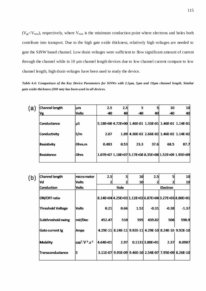
115
(Vgs<Vmin), respectively, where Vmin is the minimum conduction point where electrons and holes both
contribute into transport. Due to the high gate oxide thickness, relatively high voltages are needed to
gate the SiNW based channel. Low drain voltages were sufficient to flow significant amount of current
through the channel while in 10 µm channel length devices due to low channel current compare to low
channel length, high drain voltages have been used to study the device.
Table 4.4: Comparison of the Key Device Parameters for SiNWs with 2.5µm, 5µm and 10µm channel length. Similar
gate oxide thickness (300 nm) has been used in all devices.
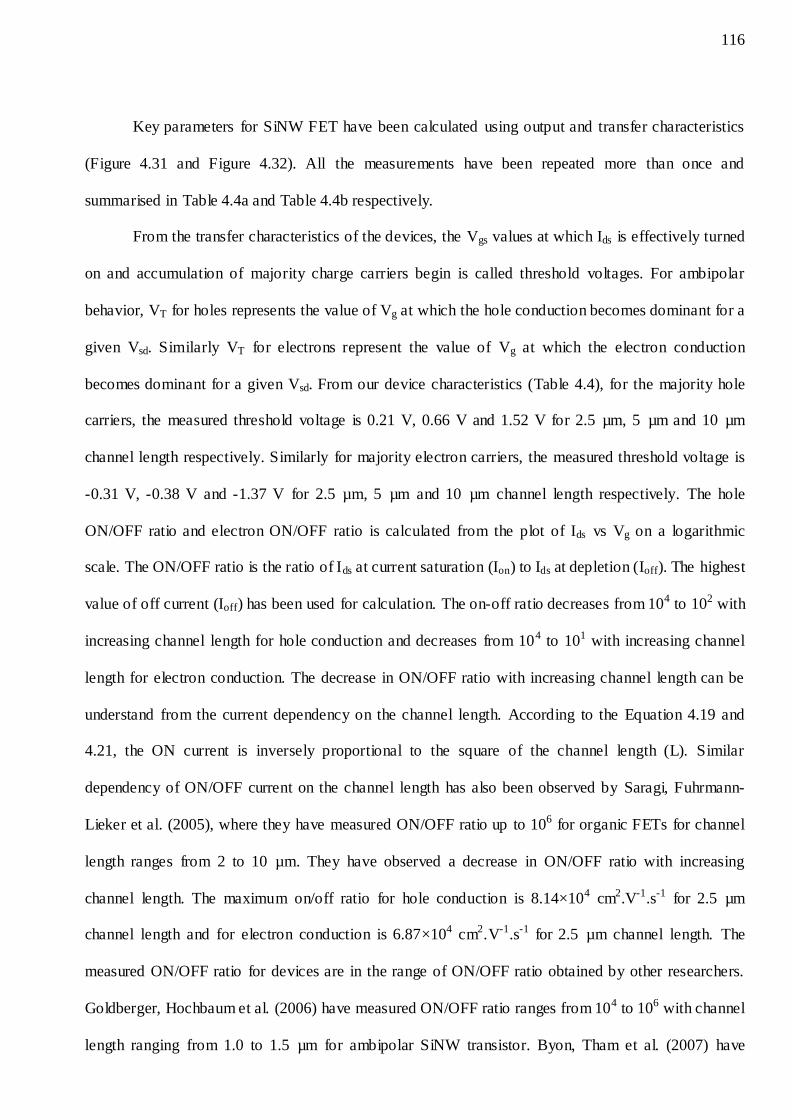
116
Key parameters for SiNW FET have been calculated using output and transfer characteristics
(Figure 4.31 and Figure 4.32). All the measurements have been repeated more than once and
summarised in Table 4.4a and Table 4.4b respectively.
From the transfer characteristics of the devices, the Vgs values at which Ids is effectively turned
on and accumulation of majority charge carriers begin is called threshold voltages. For ambipolar
behavior, VT for holes represents the value of Vg at which the hole conduction becomes dominant for a
given Vsd. Similarly VT for electrons represent the value of Vg at which the electron conduction
becomes dominant for a given Vsd. From our device characteristics (Table 4.4), for the majority hole
carriers, the measured threshold voltage is 0.21 V, 0.66 V and 1.52 V for 2.5 µm, 5 µm and 10 µm
channel length respectively. Similarly for majority electron carriers, the measured threshold voltage is
-0.31 V, -0.38 V and -1.37 V for 2.5 µm, 5 µm and 10 µm channel length respectively. The hole
ON/OFF ratio and electron ON/OFF ratio is calculated from the plot of Ids vs Vg on a logarithmic
scale. The ON/OFF ratio is the ratio of Ids at current saturation (Ion) to Ids at depletion (Ioff). The highest
value of off current (Ioff) has been used for calculation. The on-off ratio decreases from 104 to 102 with
increasing channel length for hole conduction and decreases from 104 to 101 with increasing channel
length for electron conduction. The decrease in ON/OFF ratio with increasing channel length can be
understand from the current dependency on the channel length. According to the Equation 4.19 and
4.21, the ON current is inversely proportional to the square of the channel length (L). Similar
dependency of ON/OFF current on the channel length has also been observed by Saragi, Fuhrmann-
Lieker et al. (2005), where they have measured ON/OFF ratio up to 106 for organic FETs for channel
length ranges from 2 to 10 µm. They have observed a decrease in ON/OFF ratio with increasing
channel length. The maximum on/off ratio for hole conduction is 8.14×104 cm2.V-1.s-1 for 2.5 µm
channel length and for electron conduction is 6.87×104 cm2.V-1.s-1 for 2.5 µm channel length. The
measured ON/OFF ratio for devices are in the range of ON/OFF ratio obtained by other researchers.
Goldberger, Hochbaum et al. (2006) have measured ON/OFF ratio ranges from 104 to 106 with channel
length ranging from 1.0 to 1.5 µm for ambipolar SiNW transistor. Byon, Tham et al. (2007) have
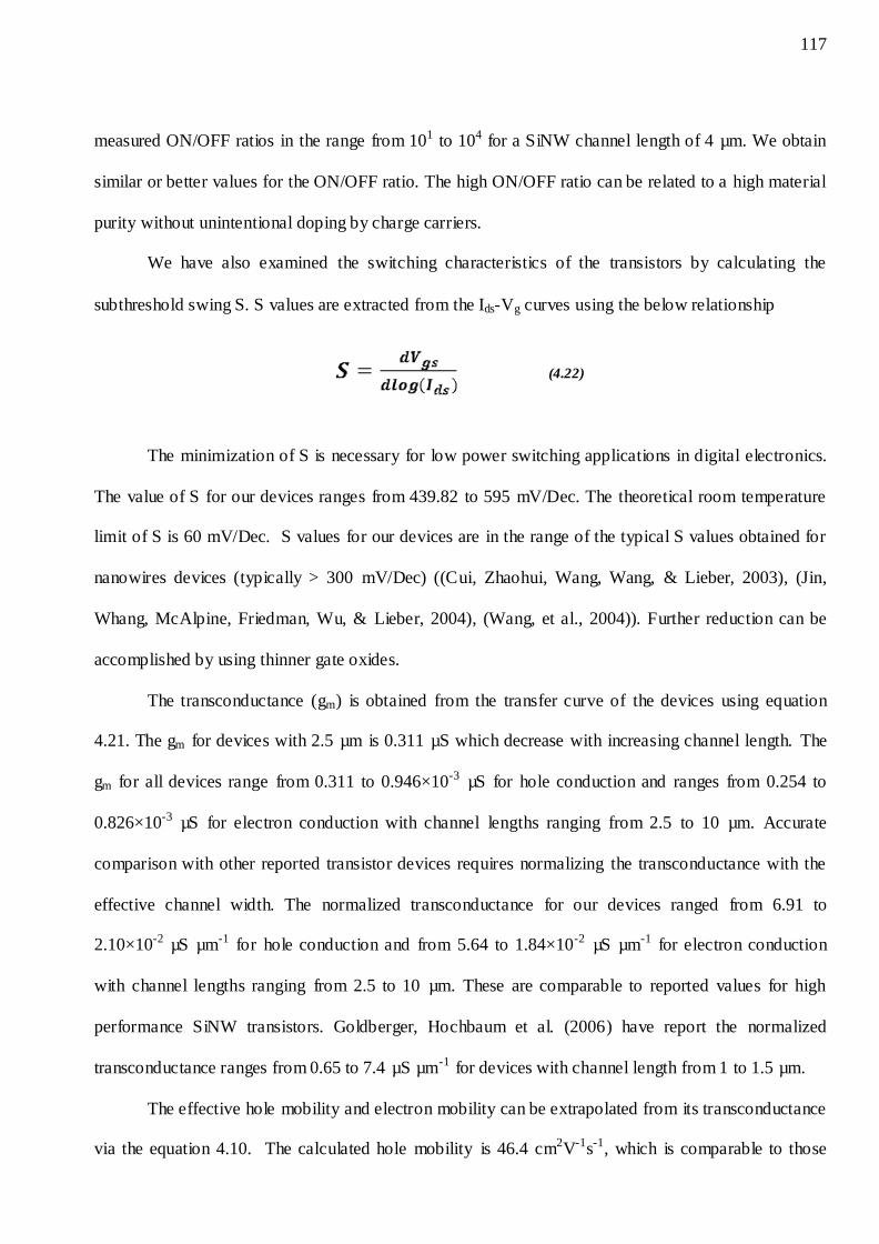
117
measured ON/OFF ratios in the range from 101 to 104 for a SiNW channel length of 4 µm. We obtain
similar or better values for the ON/OFF ratio. The high ON/OFF ratio can be related to a high material
purity without unintentional doping by charge carriers.
We have also examined the switching characteristics of the transistors by calculating the
subthreshold swing S. S values are extracted from the Ids-Vg curves using the below relationship
(4.22)
The minimization of S is necessary for low power switching applications in digital electronics.
The value of S for our devices ranges from 439.82 to 595 mV/Dec. The theoretical room temperature
limit of S is 60 mV/Dec. S values for our devices are in the range of the typical S values obtained for
nanowires devices (typically > 300 mV/Dec) ((Cui, Zhaohui, Wang, Wang, & Lieber, 2003), (Jin,
Whang, McAlpine, Friedman, Wu, & Lieber, 2004), (Wang, et al., 2004)). Further reduction can be
accomplished by using thinner gate oxides.
The transconductance (gm) is obtained from the transfer curve of the devices using equation
4.21. The gm for devices with 2.5 µm is 0.311 µS which decrease with increasing channel length. The
gm for all devices range from 0.311 to 0.946×10⁻³ µS for hole conduction and ranges from 0.254 to
0.826×10⁻³ µS for electron conduction with channel lengths ranging from 2.5 to 10 µm. Accurate
comparison with other reported transistor devices requires normalizing the transconductance with the
effective channel width. The normalized transconductance for our devices ranged from 6.91 to
2.10×10⁻² µS µm-1 for hole conduction and from 5.64 to 1.84×10⁻² µS µm-1 for electron conduction
with channel lengths ranging from 2.5 to 10 µm. These are comparable to reported values for high
performance SiNW transistors. Goldberger, Hochbaum et al. (2006) have report the normalized
transconductance ranges from 0.65 to 7.4 µS µm-1 for devices with channel length from 1 to 1.5 µm.
The effective hole mobility and electron mobility can be extrapolated from its transconductance
via the equation 4.10. The calculated hole mobility is 46.4 cm2V-1s-1, which is comparable to those
118
reported for unfunctionalized p-type silicon nanowires (10-1350 cm2V-1s-1) (Cui, Zhong et al. 2003;
Wu, Xiang et al. 2004; Byon, Tham et al. 2007). Goldberger, Hochbaum et al. (2006) have reported
hole mobilities from 7.5 to 102 cm2V-1s-1 for high performance SiNW devices. Similarly the calculated
electron mobility is 38 cm2V-1s-1 for a 2.5 µm channel length which is in the range of the mobilities
reported for n-type silicon nanowires (Byon, Tham et al. 2007; Colinge, Lee et al. 2010).
4.5 Conclusions
Silicon nanowire synthesis has been discussed in this chapter, starting with the
synthesis of silicon oxide nanowires. We have developed a novel method for the large scale synthesis
of core-clad crystalline silicon nanowires by combining the SLS and VLS growth mechanisms. We
have produced silica nanowires, obtained from the thermal annealing of Ni/Si, Ni/SiO2/Si and
Ni/Ti/SiO2/Si in a furnace at 1000oC in a He and H2 environment. The He is needed for cooling down
the chamber while H2 facilitates the nanowire growth. The nanowires also contain some crystalline
silicon, as determined by the Raman measurements. The Raman peak has been observed in our
samples and the phonon confinement model employed to measure the diameter of the Si rich tail in our
samples. The Raman peak shift and FWHM variation with nanowire diameter qualitatively follow the
phonon confinement model. We conclude that the Ni acts as the catalyst material, essential for
nanowire growth, and the Ti can be used to form and control the ratio of Type I to type II nanowires.
The nanowire diameter can be controlled by the thickness of the metal layers in the seedbed, much like
carbon nanotube growth on a Ni catalyst (Poa, Henley et al. 2005). An inverse relation has been
observed (both for Ni and Ti), but not by the SiO2 layer. The diameter changes by ~-29% for a given
change in the metal thickness for thickness up to 50 nm. We have explained the growth mechanism in
terms of three stages: (1) a island formation stage followed by (2) initial nanowire growth by a SLS
process and continued by (3) a VLS growth process. The importance of the ambient step has been
highlighted in terms of enabling growth by silicon-carrier gas diffusion to the tip of the nanowires.
119
Crystalline SiNWs have been grown with two catalysts (Au and Ni). Metal islands serve as a starting
point of the growth as well as facilitating the SiO formation which further decomposes and nanowire
growth takes place. The presence of the catalyst head at the tip from TEM images suggests the growth
occurs via a VLS mechanism. HRTEM images show the crystalline Si core covered with an oxide. A
detailed Raman analysis has been conducted for both types of sample. Raman peaks of SiNWs have
been observed and identified. The spectral features for both samples have been analyzed. A calculation
based on a phonon confinement model has been performed to interpret the first order Raman-spectra.
The diameter of the nanowires has been calculated with this model. There is a discrepancy between the
calculated and experimental data. Some reasons for this discrepancy are discussed.
A top-down approach has also shown its importance in Silicon nano-pillar formation. Top-down
approaches use masking which is followed by etching. Nano partic les have been used for nano dot
mask formation where the diameter of the nano-pillars can be controlled by choosing different
diameter nano particles. A problem of coagulation was faced in this process which has resolved by
using different methods for nano dot formation. Self-organized metal island formation by low
temperature annealing can be a good solution for low cost nano dot mask formation. 10 nm Au and 20
nm Au films have been used for thermal annealing at 500oC for 30 minutes, including heating time, in
He atmosphere. A film thickness effect was observed in 20 nm Au film samples. ICP-RIE (STS)
system was use to etch Si with well known CF4 gas. Prior to the etching of Au array patterned samples,
a set of experiments were done to observe the effect of gas flow rate and gas pressure on etching. High
gas flow rates result in high concentration of fluorine ions with a resultant increase in etch rate, while
high gas pressure will decrease the mean free path resulting in a decrease in etch rates. A decrease in
anisotropy with increasing gas pressure was also observed. For anisotropic Si etching, the optimum
condition of etching was 30sccm CF4 flow rate and 2 mTorr gas pressure.
The electrical properties of the core-clad crystalline silicon nanowires have been uncovered
from FETs made with SiNW-Ni channel. These devices have shown ambipolar behavior with mobility
values which are in the range of mobilities reported for the devices made with n- and p-type SiNWs.
120
Ambipolar SiNWs FET are one of the most promising candidates for future nanoelectronic
applications. An ambipolar FET makes them attractive due to their ability to work as either p-type or
n-type FET by implementing different top gate metals and asymmetric design as shown by Chen,
Appenzeller et al. (2006) in their ambipolar carbon nanotubes FETs. The ambipolar behavior is
attributed to the accumulation of holes with negative gate bias and to inversion of electrons with a
positive gate bias and also shows the intrinsic nature of the material.
121
5 Carbon Nanotube Synthesis
After the successful growth of crystalline silicon nanowires, we examined the synthesis of
carbon nanotubes to reach the objective of the growth of Si/C heterojunctions. CVD gives an
opportunity to grow CNTs with accurate positioning wherever desired with product purity and large
scale production capability. According to the plan, CNTs have to be grown from the tip of the SiNW
which has a Ni catalysts on the tip. It restricted us to using Ni as the catalyst for CNT growth, which
may form nickel silicide during growth.
5.1 CNT growth with methane as carbon feedstock
A set of experiments were planned to grow the CNTs with Ni catalyst. The main objective was
to synthesize the CNTs with nickel-silicide catalyst in the same system that had been used to grow
SiNWs to reduce the chance of post oxidization of the SiNWs in atmosphere. The growth temperature
of CNTs by Ni deposited directly on Si substrate produces a reaction between the Si substrate and
nickel catalyst, thus changes the pure nickel catalyst into nickel-silicide with the modification in the
catalytic activity of nickel for CNT growth. Several researchers (Teo, Chhowalla et al. 2001; Jeong,
Jeong et al. 2002; Siegal, Overmyer et al. 2002) have shown the requirement of the diffusion barrier
layer between the underlying Si and the Ni layer, to maintain the ‗active‘ Ni particles for CNT growth
and to prevent the formation of nickel silicide at higher temperatures. Furthermore, other groups have
reported again the requirement of a barrier layer such as SiO2 to prevent silicide formation when nickel
has been used as a catalyst for CNT growth. Several other researchers (Ducati, Alexandrou et al. 2002;
Siegal, Overmyer et al. 2002; Teo, Chhowalla et al. 2002; Milne, Teo et al. 2003) have also shown the
requirement of a barrier layer between Ni and Si substrate to prevent the nickel-silicide formation for
CNT growth. On the other hand, several researchers (Choi, Cho et al. 2002; Mizuhisa, Kawabata et al.
2003; Kabir and et al. 2005) have shown CNT growth with nickel silicide catalyst. Choi, Cho et al.
122
(2002) has observed growth of CNTs with the formation of nickel silicide at temperatures ranging
from 500 to 900oC with C2H2 as a carbon feedstock. Mizuhisa, Kawabata et al. (2003) has shown the
growth of bundles of CNTs with nickel silicide as a catalyst with the control of the diameter of CNTs
by forming various nickel silicide phases. Kabir et al. (2005) has observed a significant improvement
in CNT growth on different metal underlayers, by introducing a Si layer between the metal catalyst
layer and metal underlayer. Nihei, Kawabata et al. ( 2003) have used nickel-silicide as a catalyst to
grow bundles of CNTs and suggested that the CNT diameter might be controlled by forming various
nickel-silicide phases. However, the catalytic activity of nickel silicide is still a subject of some debate.
Several researchers have prevented nickel-silicide formation during CNT growth. But simultaneously
others have used nickel-silicide as the catalyst for the CNT growth. These suggest the growth of CNTs
with nickel-silicide as catalyst under certain experimental conditions. Our work reveals that under
selected growth conditions, nickel-silicide can act as active catalyst and further provide for CNT
formation. No barrier layer has been used between the nickel and Si substrate allowing the formation
of nickel-silicide and use it as a catalyst for CNT growth. The nickel deposition was performed using a
DC-magnetron sputtering system (JLS), using argon at a pressure of 5 mTorr with 25 sccm flow rate.
The substrates were p-type <100> single crystal Si. Various thicknesses of Ni (2 nm, 5 nm, 10 nm)
were deposited on the wafer.
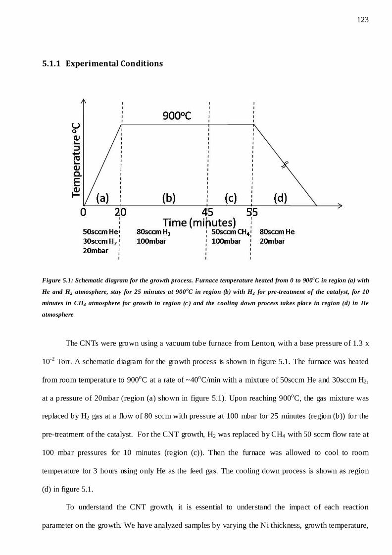
123
5.1.1 Experimental Conditions
Figure 5.1: Schematic diagram for the growth process. Furnace temperature heated from 0 to 900oC in region (a) with
He and H2 atmosphere, stay for 25 minutes at 900oC in region (b) with H2 for pre-treatment of the catalyst, for 10
minutes in CH4 atmosphere for growth in region (c ) and the cooling down process takes place in region (d) in He
atmosphere
The CNTs were grown using a vacuum tube furnace from Lenton, with a base pressure of 1.3 x
10-2 Torr. A schematic diagram for the growth process is shown in figure 5.1. The furnace was heated
from room temperature to 900oC at a rate of ~40oC/min with a mixture of 50sccm He and 30sccm H2,
at a pressure of 20mbar (region (a) shown in figure 5.1). Upon reaching 900oC, the gas mixture was
replaced by H2 gas at a flow of 80 sccm with pressure at 100 mbar for 25 minutes (region (b)) for the
pre-treatment of the catalyst. For the CNT growth, H2 was replaced by CH4 with 50 sccm flow rate at
100 mbar pressures for 10 minutes (region (c)). Then the furnace was allowed to cool to room
temperature for 3 hours using only He as the feed gas. The cooling down process is shown as region
(d) in figure 5.1.
To understand the CNT growth, it is essential to understand the impact of each reaction
parameter on the growth. We have analyzed samples by varying the Ni thickness, growth temperature,
124
pre-treatment time and process pressure. The nickel thickness was varied, using 2 nm, 5 nm and 10 nm
films to understand the effect of thickness on growth and to achieve the des ired growth. The growth
temperature was varied from 850oC to 1000oC in 50oC steps. The effect of pre-treatment time has been
observed by varying the time with 15 minutes, 20 minutes, 25 minutes and 30 minutes. The H2 flow
rate was kept constant at 80 sccm throughout the experiment to coincide this growth with SiNWs
growth. The chamber pressure was varied with CNT growth at 0 mbar, 50 mbar, 100 mbar and 150
mbar.
5.1.2 Results and Discussion
In order to make a quantitative analysis of different samples, a statistical analysis of the top-
view SEM images was performed. A FEI Quanta 200 scanning electron microscope (SEM) was used
to image the nanowires. The optical properties were analyzed by micro Raman analysis (Renishaw
2000) using a diode laser as the excitation source (514 nm).
5.1.2.1 Effect of Nickel thickness on the growth
The effect of the Ni thickness on the growth of CNTs has been analysed with SEM images and
Raman spectra. Figure 5.2 presents the SEM images and Raman spectra for CNTs grown samples with
2, 5 and 10 nm Ni thicknesses.
Uniform CNT growth has been observed over the entire sample area in terms of diameter and
length. The catalyst particles were clearly observed on the tip of the CNTs, indicated that a tip growth
mechanism took place. As the Ni thickness increased in the range of 2, 5 and 10 nm, the particle size
increased to 88, 155 and 180 nm respectively. It was considered that the initial Ni thickness
determined the size and density of the island catalyst which determined the size and density of the
CNTs. A similar observation has been made by Chhowalla, Teo et al. (2001).
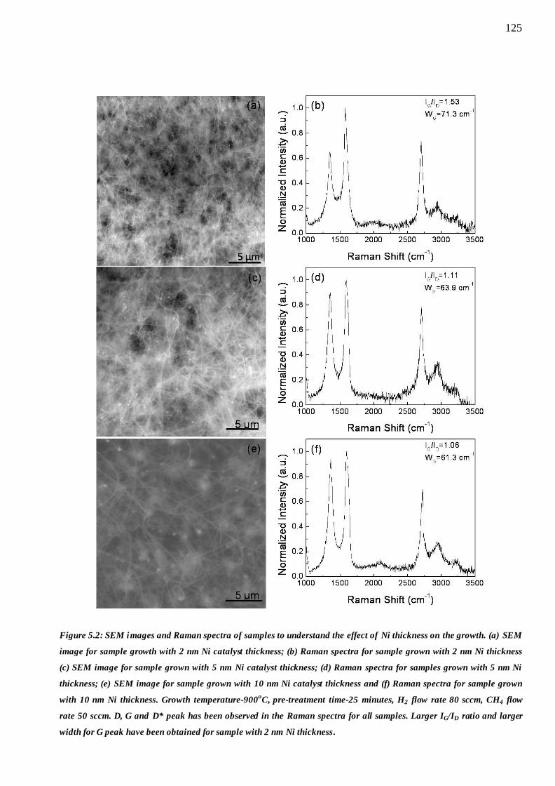
125
Figure 5.2: SEM images and Raman spectra of samples to understand the effect of Ni thickness on the growth. (a) SEM
image for sample growth with 2 nm Ni catalyst thickness; (b) Raman spectra for sample grown with 2 nm Ni thickness
(c) SEM image for sample grown with 5 nm Ni catalyst thickness; (d) Raman spectra for samples grown with 5 nm Ni
thickness; (e) SEM image for sample grown with 10 nm Ni catalyst thickness and (f) Raman spectra for sample grown
with 10 nm Ni thickness. Growth temperature-900oC, pre-treatment time-25 minutes, H2 flow rate 80 sccm, CH4 flow
rate 50 sccm. D, G and D* peak has been observed in the Raman spectra for all samples. Larger IG/ID ratio and larger
width for G peak have been obtained for sample with 2 nm Ni thickness.
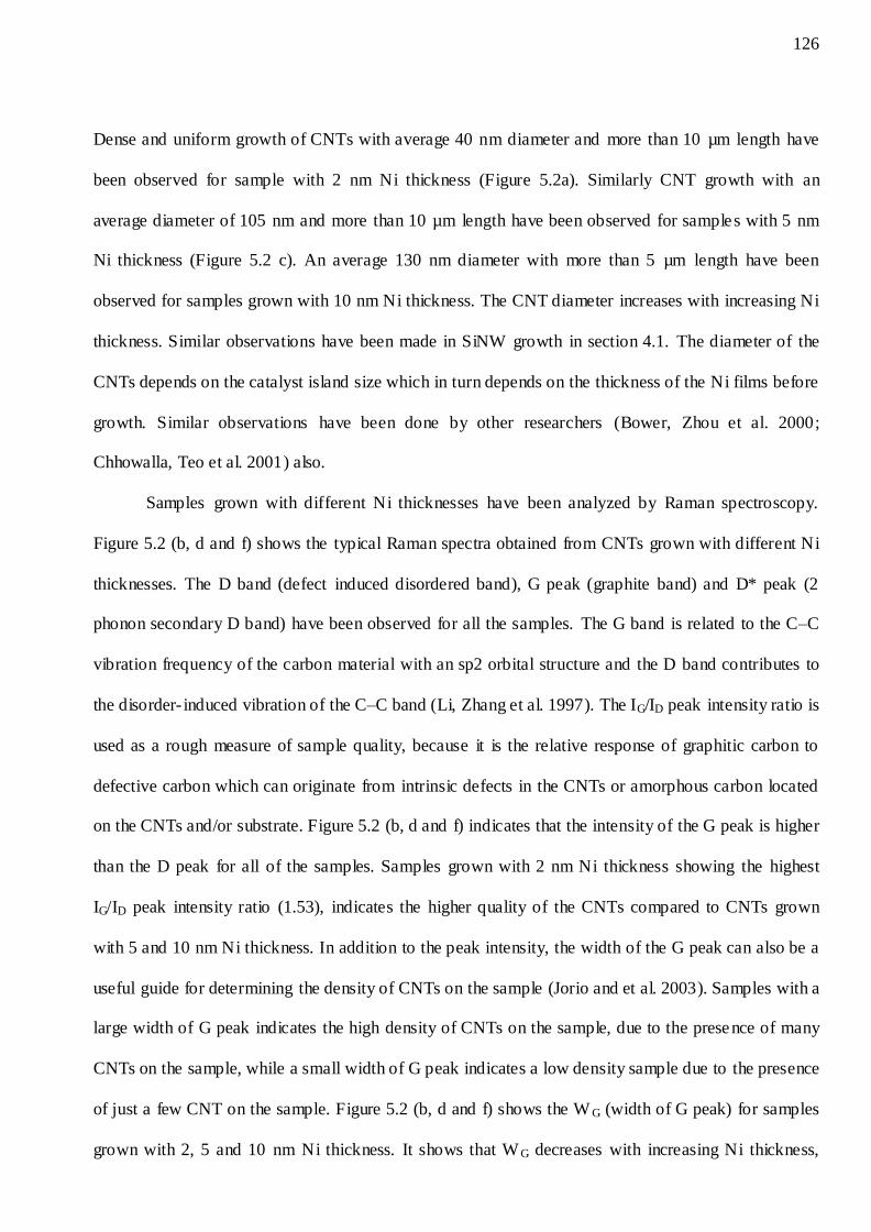
126
Dense and uniform growth of CNTs with average 40 nm diameter and more than 10 µm length have
been observed for sample with 2 nm Ni thickness (Figure 5.2a). Similarly CNT growth with an
average diameter of 105 nm and more than 10 µm length have been observed for samples with 5 nm
Ni thickness (Figure 5.2 c). An average 130 nm diameter with more than 5 µm length have been
observed for samples grown with 10 nm Ni thickness. The CNT diameter increases with increasing Ni
thickness. Similar observations have been made in SiNW growth in section 4.1. The diameter of the
CNTs depends on the catalyst island size which in turn depends on the thickness of the Ni films before
growth. Similar observations have been done by other researchers (Bower, Zhou et al. 2000;
Chhowalla, Teo et al. 2001) also.
Samples grown with different Ni thicknesses have been analyzed by Raman spectroscopy.
Figure 5.2 (b, d and f) shows the typical Raman spectra obtained from CNTs grown with different Ni
thicknesses. The D band (defect induced disordered band), G peak (graphite band) and D* peak (2
phonon secondary D band) have been observed for all the samples. The G band is related to the C–C
vibration frequency of the carbon material with an sp2 orbital structure and the D band contributes to
the disorder- induced vibration of the C–C band (Li, Zhang et al. 1997). The IG/ID peak intensity ratio is
used as a rough measure of sample quality, because it is the relative response of graphitic carbon to
defective carbon which can originate from intrinsic defects in the CNTs or amorphous carbon located
on the CNTs and/or substrate. Figure 5.2 (b, d and f) indicates that the intensity of the G peak is higher
than the D peak for all of the samples. Samples grown with 2 nm Ni thickness showing the highest
IG/ID peak intensity ratio (1.53), indicates the higher quality of the CNTs compared to CNTs grown
with 5 and 10 nm Ni thickness. In addition to the peak intensity, the width of the G peak can also be a
useful guide for determining the density of CNTs on the sample (Jorio and et al. 2003). Samples with a
large width of G peak indicates the high density of CNTs on the sample, due to the presence of many
CNTs on the sample, while a small width of G peak indicates a low density sample due to the presence
of just a few CNT on the sample. Figure 5.2 (b, d and f) shows the W G (width of G peak) for samples
grown with 2, 5 and 10 nm Ni thickness. It shows that W G decreases with increasing Ni thickness,
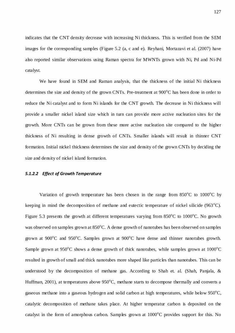
127
indicates that the CNT density decrease with increasing Ni thickness. This is verified from the SEM
images for the corresponding samples (Figure 5.2 (a, c and e). Reyhani, Mortazavi et al. (2007) have
also reported similar observations using Raman spectra for MWNTs grown with Ni, Pd and Ni-Pd
catalyst.
We have found in SEM and Raman analysis, that the thickness of the initial Ni thickness
determines the size and density of the grown CNTs. Pre-treatment at 900oC has been done in order to
reduce the Ni catalyst and to form Ni islands for the CNT growth. The decrease in Ni thickness will
provide a smaller nickel island size which in turn can provide more active nucleation sites for the
growth. More CNTs can be grown from these more active nucleation site compared to the higher
thickness of Ni resulting in dense growth of CNTs. Smaller islands will result in thinner CNT
formation. Initial nickel thickness determines the size and density of the grown CNTs by deciding the
size and density of nickel island formation.
5.1.2.2 Effect of Growth Temperature
Variation of growth temperature has been chosen in the range from 850oC to 1000oC by
keeping in mind the decomposition of methane and eutectic temperature of nickel silicide (963oC).
Figure 5.3 presents the growth at different temperatures varying from 850oC to 1000oC. No growth
was observed on samples grown at 850oC. A dense growth of nanotubes has been observed on samples
grown at 900oC and 950oC. Samples grown at 900oC have dense and thinner nanotubes growth.
Sample grown at 950oC shows a dense growth of thick nanotubes, while samples grown at 1000oC
resulted in growth of small and thick nanotubes more shaped like particles than nanotubes. This can be
understood by the decomposition of methane gas. According to Shah et. al. (Shah, Panjala, &
Huffman, 2001), at temperatures above 950oC, methane starts to decompose thermally and converts a
gaseous methane into a gaseous hydrogen and solid carbon at high temperatures, while below 950oC,
catalytic decomposition of methane takes place. At higher temperatur carbon is deposited on the
catalyst in the form of amorphous carbon. Samples grown at 1000oC provides support for this. No
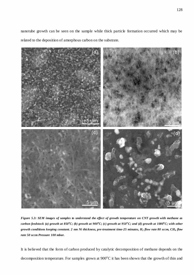
128
nanotube growth can be seen on the sample while thick particle formation occurred which may be
related to the deposition of amorphous carbon on the substrate.
Figure 5.3: SEM images of samples to understand the effect of growth temperature on CNT growth with methane as
carbon feedstock (a) growth at 850oC; (b) growth at 900
oC; (c) growth at 950
oC; and (d) growth at 1000
oC; with other
growth conditions keeping constant. 2 nm Ni thickness, pre-treatment time-25 minutes, H2 flow rate 80 sccm, CH4 flow
rate 50 sccm Pressure 100 mbar.
It is believed that the form of carbon produced by catalytic decomposition of methane depends on the
decomposition temperature. For samples grown at 900oC it has been shown that the growth of thin and
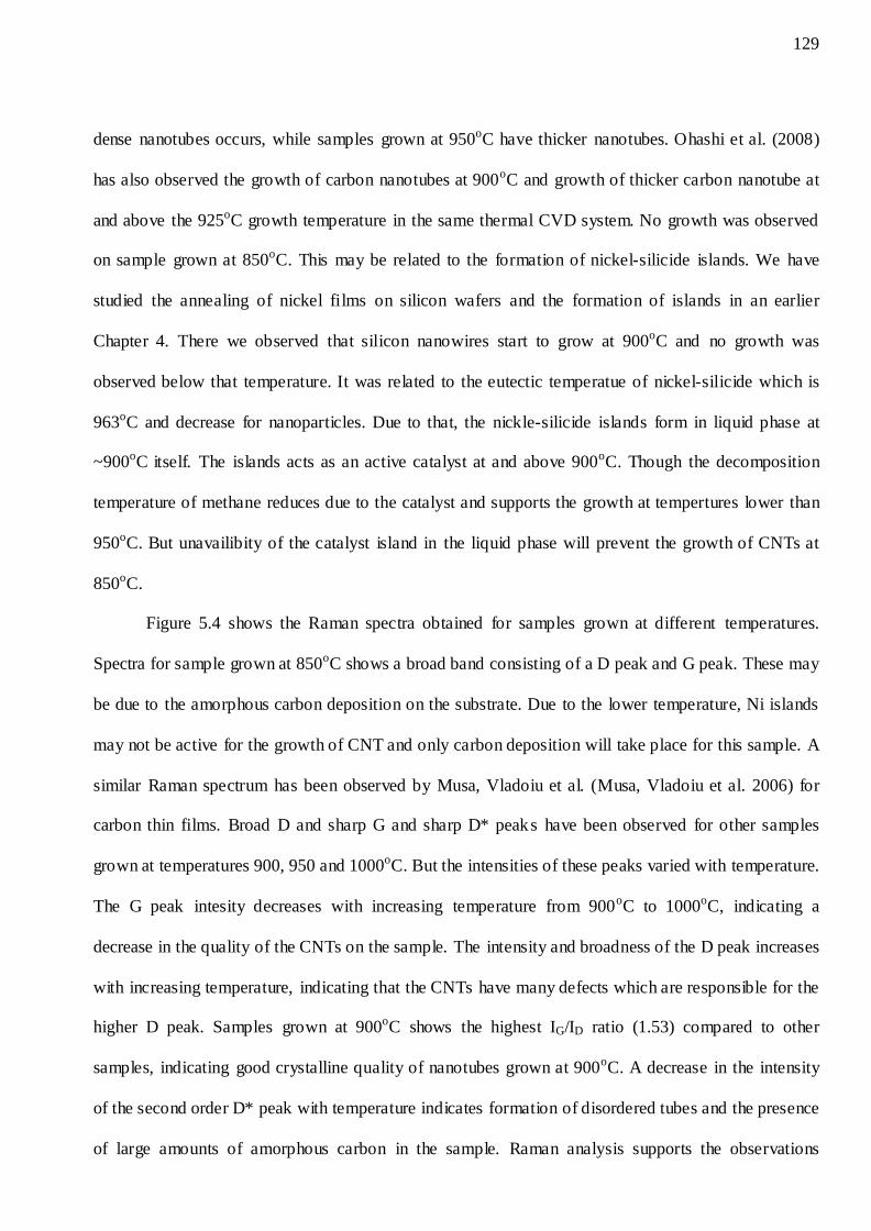
129
dense nanotubes occurs, while samples grown at 950oC have thicker nanotubes. Ohashi et al. (2008)
has also observed the growth of carbon nanotubes at 900oC and growth of thicker carbon nanotube at
and above the 925oC growth temperature in the same thermal CVD system. No growth was observed
on sample grown at 850oC. This may be related to the formation of nickel-silicide islands. We have
studied the annealing of nickel films on silicon wafers and the formation of islands in an earlier
Chapter 4. There we observed that silicon nanowires start to grow at 900oC and no growth was
observed below that temperature. It was related to the eutectic temperatue of nickel-silicide which is
963oC and decrease for nanoparticles. Due to that, the nickle-silicide islands form in liquid phase at
~900oC itself. The islands acts as an active catalyst at and above 900oC. Though the decomposition
temperature of methane reduces due to the catalyst and supports the growth at tempertures lower than
950oC. But unavailibity of the catalyst island in the liquid phase will prevent the growth of CNTs at
850oC.
Figure 5.4 shows the Raman spectra obtained for samples grown at different temperatures.
Spectra for sample grown at 850oC shows a broad band consisting of a D peak and G peak. These may
be due to the amorphous carbon deposition on the substrate. Due to the lower temperature, Ni islands
may not be active for the growth of CNT and only carbon deposition will take place for this sample. A
similar Raman spectrum has been observed by Musa, Vladoiu et al. (Musa, Vladoiu et al. 2006) for
carbon thin films. Broad D and sharp G and sharp D* peaks have been observed for other samples
grown at temperatures 900, 950 and 1000oC. But the intensities of these peaks varied with temperature.
The G peak intesity decreases with increasing temperature from 900oC to 1000oC, indicating a
decrease in the quality of the CNTs on the sample. The intensity and broadness of the D peak increases
with increasing temperature, indicating that the CNTs have many defects which are responsible for the
higher D peak. Samples grown at 900oC shows the highest IG/ID ratio (1.53) compared to other
samples, indicating good crystalline quality of nanotubes grown at 900oC. A decrease in the intensity
of the second order D* peak with temperature indicates formation of disordered tubes and the presence
of large amounts of amorphous carbon in the sample. Raman analysis supports the observations
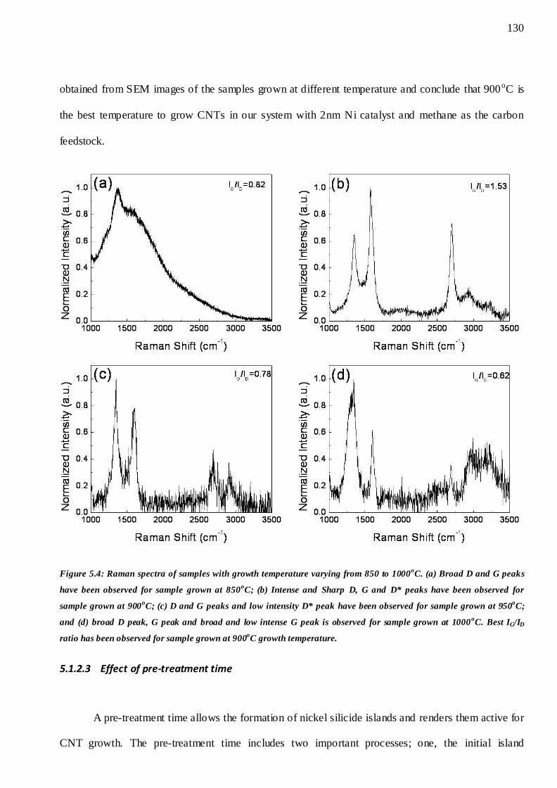
130
obtained from SEM images of the samples grown at different temperature and conclude that 900oC is
the best temperature to grow CNTs in our system with 2nm Ni catalyst and methane as the carbon
feedstock.
Figure 5.4: Raman spectra of samples with growth temperature varying from 850 to 1000oC. (a) Broad D and G peaks
have been observed for sample grown at 850oC; (b) Intense and Sharp D, G and D* peaks have been observed for
sample grown at 900oC; (c) D and G peaks and low intensity D* peak have been observed for sample grown at 950
oC;
and (d) broad D peak, G peak and broad and low intense G peak is observed for sample grown at 1000oC. Best IG/ID
ratio has been observed for sample grown at 900oC growth temperature.
5.1.2.3 Effect of pre-treatment time
A pre-treatment time allows the formation of nickel silicide islands and renders them active for
CNT growth. The pre-treatment time includes two important processes; one, the initial island
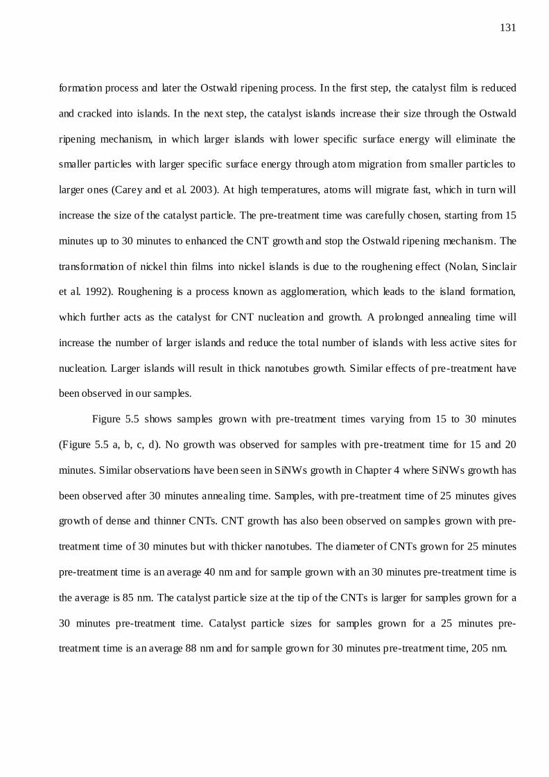
131
formation process and later the Ostwald ripening process. In the first step, the catalyst film is reduced
and cracked into islands. In the next step, the catalyst islands increase their size through the Ostwald
ripening mechanism, in which larger islands with lower specific surface energy will eliminate the
smaller particles with larger specific surface energy through atom migration from smaller particles to
larger ones (Carey and et al. 2003). At high temperatures, atoms will migrate fast, which in turn will
increase the size of the catalyst particle. The pre-treatment time was carefully chosen, starting from 15
minutes up to 30 minutes to enhanced the CNT growth and stop the Ostwald ripening mechanism. The
transformation of nickel thin films into nickel islands is due to the roughening effect (Nolan, Sinclair
et al. 1992). Roughening is a process known as agglomeration, which leads to the island formation,
which further acts as the catalyst for CNT nucleation and growth. A prolonged annealing time will
increase the number of larger islands and reduce the total number of islands with less active sites for
nucleation. Larger islands will result in thick nanotubes growth. Similar effects of pre-treatment have
been observed in our samples.
Figure 5.5 shows samples grown with pre-treatment times varying from 15 to 30 minutes
(Figure 5.5 a, b, c, d). No growth was observed for samples with pre-treatment time for 15 and 20
minutes. Similar observations have been seen in SiNWs growth in Chapter 4 where SiNWs growth has
been observed after 30 minutes annealing time. Samples, with pre-treatment time of 25 minutes gives
growth of dense and thinner CNTs. CNT growth has also been observed on samples grown with pre-
treatment time of 30 minutes but with thicker nanotubes. The diameter of CNTs grown for 25 minutes
pre-treatment time is an average 40 nm and for sample grown with an 30 minutes pre-treatment time is
the average is 85 nm. The catalyst particle size at the tip of the CNTs is larger for samples grown for a
30 minutes pre-treatment time. Catalyst particle sizes for samples grown for a 25 minutes pre-
treatment time is an average 88 nm and for sample grown for 30 minutes pre-treatment time, 205 nm.
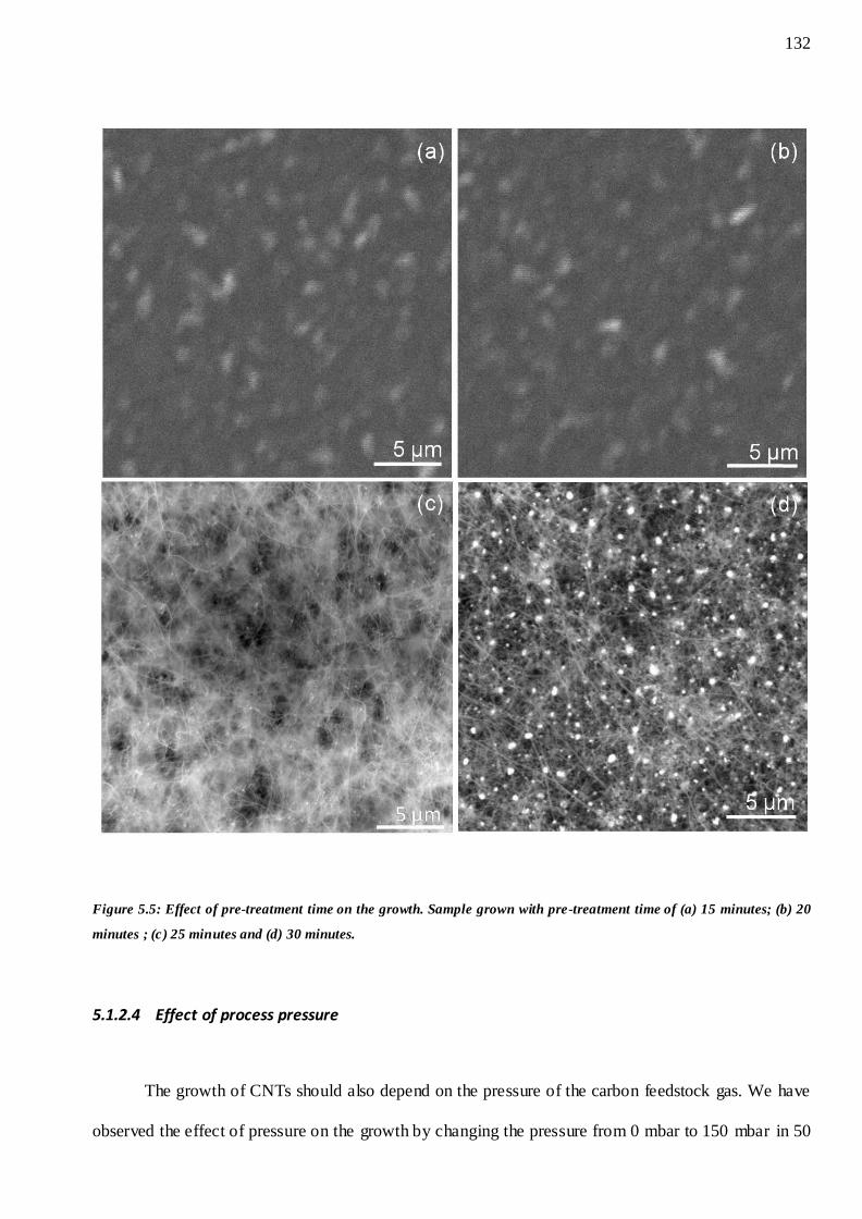
132
Figure 5.5: Effect of pre-treatment time on the growth. Sample grown with pre-treatment time of (a) 15 minutes; (b) 20
minutes ; (c) 25 minutes and (d) 30 minutes.
5.1.2.4 Effect of process pressure
The growth of CNTs should also depend on the pressure of the carbon feedstock gas. We have
observed the effect of pressure on the growth by changing the pressure from 0 mbar to 150 mbar in 50
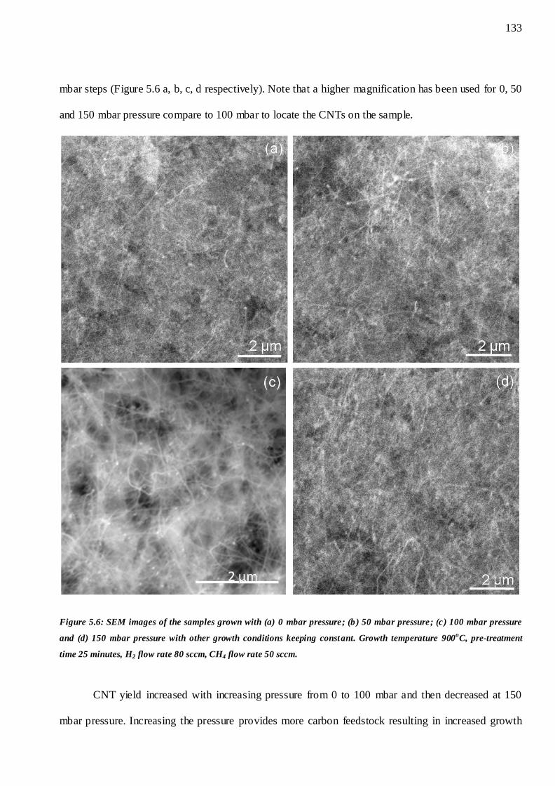
133
mbar steps (Figure 5.6 a, b, c, d respectively). Note that a higher magnification has been used for 0, 50
and 150 mbar pressure compare to 100 mbar to locate the CNTs on the sample.
Figure 5.6: SEM images of the samples grown with (a) 0 mbar pressure; (b ) 50 mbar pressure; (c) 100 mbar pressure
and (d) 150 mbar pressure with other growth conditions keeping constant. Growth temperature 900oC, pre-treatment
time 25 minutes, H2 flow rate 80 sccm, CH4 flow rate 50 sccm.
CNT yield increased with increasing pressure from 0 to 100 mbar and then decreased at 150
mbar pressure. Increasing the pressure provides more carbon feedstock resulting in increased growth
134
of CNTs. A decrease in CNT growth at 150 mbar is due to the excess carbon atoms deposited on the
surface which in turn will poison the catalyst quickly and reduce the growth of CNTs.
Carbon nanotube growth was carried out between 850 to 1000oC with pressure ranging from 0
mbar to 150 mbar. After understanding and analyzing the effect of each parameter on the growth,
insight into the growth mechanism has been obtained. The growth of CNTs by the CVD process over
metal catalysts includes (i) decomposition of hydrocarbon gas, (ii) incorporation of carbon atoms into
the transition metal catalysts and (iii) diffusion of carbon atoms in the transition metal catalyst to form
the nuclei for CNTs. During the growth of CNTs, two mechanisms involving the base growth and tip
growth mode could exist. By observation of SEM images, the growth of CNTs in our case could
follow the tip growth mode. Firstly the nickel thin film is broken up into nickel silicide island s by
roughening. A limited time of pre-treatment (25 minutes) allows the formation of small island and will
stop the formation of larger island due to Ostwald ripening. Next, the nucleation of carbon
nanostructure proceeds after the nano island formation. Catalytic decomposition of methane provides
the carbon feedstock. The carbon diffuses onto the nickel silicide island. The diffusion is likely to be
surface based rather than through the bulk of the nickel particle due to the lower activation energy of
the carbon surface diffusion compared to that of bulk diffusion. The surface diffusion of carbon then
lifts the island as the growth proceeds. Higher process pressure provides more carbon which poisons
the catalyst and decreases the growth. Similarly, higher process temperature will be favorable for
thermal decomposition of methane which results in amorphous carbon deposition on the substrate.
Carefully chosen growth parameters will give successful growth of CNTs with nickel silicide catalyst.
In this Chapter we will refer to these CNTs as CNTmethane. Similar growth parameters will be used to
grow CNTs at SiNWs with nickel-silicide tip to grow SiNW/CNT heterojunction.
135
5.2 CNT growth with acetylene as carbon feedstock
Silicon nanopillars have been synthesized on Si wafers with ICP etching, details of which is
described in Chapter 4. To fulfill the requirement of the heterojunction formation with Si nanopillars,
CNTs need to be grown at the tip of the nanopillars. CNT growth has been achieved in a TCVD
system with methane as the carbon feedstock at 900oC temperature. High growth temperatures may
destroy the form and properties of the Si nanopillars. Due to the high growth temperature, we need
another growth condition to grow CNTs at the tip of the Si nanopillars. To satisfy this requirement, a
DC-PECVD system equipped with acetylene was used to grow CNTs. As the decomposition
temperature of methane is very high it makes it unfavorable for CNT growth at low temperature.
Acetylene breaks down at lower temperatures compared to methane, leading to the CNTs growth at
comparatively lower temperature. Most reports of CNT synthesis at low temperature describes the use
of acetylene as the carbon feedstock for the growth. Fe has been used as a catalyst in this experiment
due to its proven ability for CNT growth at low temperature. 5 nm Fe deposited on a 300 nm oxide
coated silicon wafer was used in this experiment. To obtain the desired growth, experimental
conditions have been chosen carefully on the basis of the SiNW and CNT growth experience and on
the basis of the literature review.
5.2.1 Experimental Conditions
The CNTs were grown using a parallel-plate direct current-PECVD system, with a base
pressure of 10-3 Torr with acetylene as the carbon feedstock and H2 as the dilution gas. A typical run
was started with the backfilling of the evacuated chamber to the desired operating pressure (2 Torr)
with H2. A schematic diagram for the growth process is shown in figure 5.7. The system was kept at
500oC for 10 minutes in H2 atmosphere with 100sccm flow rate (region (a) shown in figure 5.8) for the
pre-treatment of the catalyst. For the CNT growth, 5% of C2H2 with 5 sccm flow rate was added to the
chamber for 5 minutes (region (b)). Then the furnace was allowed to cool to room temperature using
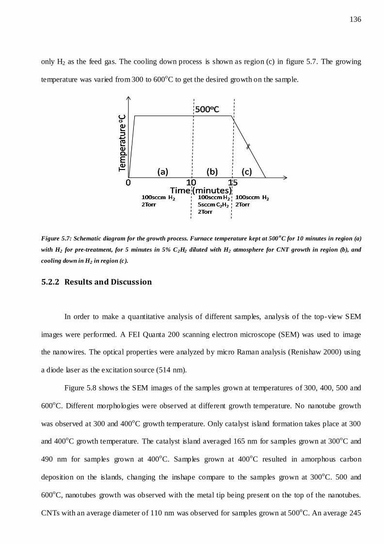
136
only H2 as the feed gas. The cooling down process is shown as region (c) in figure 5.7. The growing
temperature was varied from 300 to 600oC to get the desired growth on the sample.
Figure 5.7: Schematic diagram for the growth process. Furnace temperature kept at 500oC for 10 minutes in region (a)
with H2 for pre-treatment, for 5 minutes in 5% C2H2 diluted with H2 atmosphere for CNT growth in region (b), and
cooling down in H2 in region (c).
5.2.2 Results and Discussion
In order to make a quantitative analysis of different samples, analysis of the top-view SEM
images were performed. A FEI Quanta 200 scanning electron microscope (SEM) was used to image
the nanowires. The optical properties were analyzed by micro Raman analysis (Renishaw 2000) using
a diode laser as the excitation source (514 nm).
Figure 5.8 shows the SEM images of the samples grown at temperatures of 300, 400, 500 and
600oC. Different morphologies were observed at different growth temperature. No nanotube growth
was observed at 300 and 400oC growth temperature. Only catalyst island formation takes place at 300
and 400oC growth temperature. The catalyst island averaged 165 nm for samples grown at 300oC and
490 nm for samples grown at 400oC. Samples grown at 400oC resulted in amorphous carbon
deposition on the islands, changing the inshape compare to the samples grown at 300oC. 500 and
600oC, nanotubes growth was observed with the metal tip being present on the top of the nanotubes.
CNTs with an average diameter of 110 nm was observed for samples grown at 500oC. An average 245
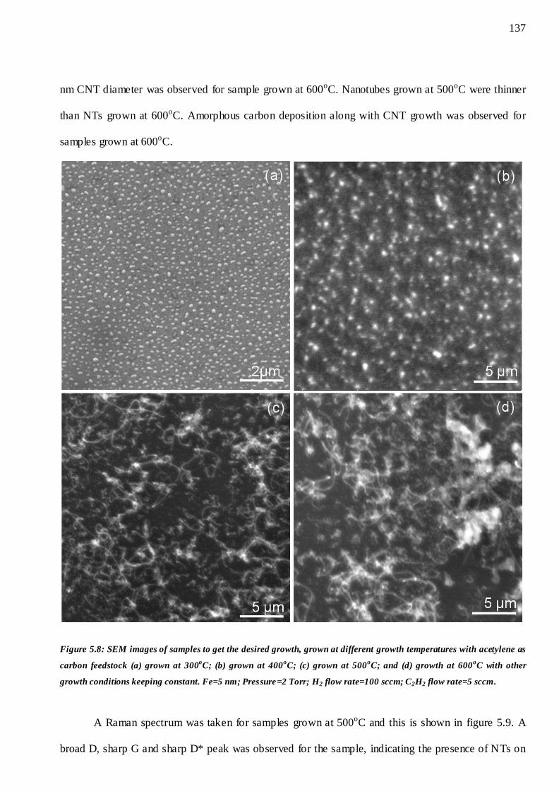
137
nm CNT diameter was observed for sample grown at 600oC. Nanotubes grown at 500oC were thinner
than NTs grown at 600oC. Amorphous carbon deposition along with CNT growth was observed for
samples grown at 600oC.
Figure 5.8: SEM images of samples to get the desired growth, grown at different growth temperatures with acetylene as
carbon feedstock (a) grown at 300oC; (b) grown at 400
oC; (c) grown at 500
oC; and (d) growth at 600
oC with other
growth conditions keeping constant. Fe=5 nm; Pressure=2 Torr; H2 flow rate=100 sccm; C2H2 flow rate=5 sccm.
A Raman spectrum was taken for samples grown at 500oC and this is shown in figure 5.9. A
broad D, sharp G and sharp D* peak was observed for the sample, indicating the presence of NTs on
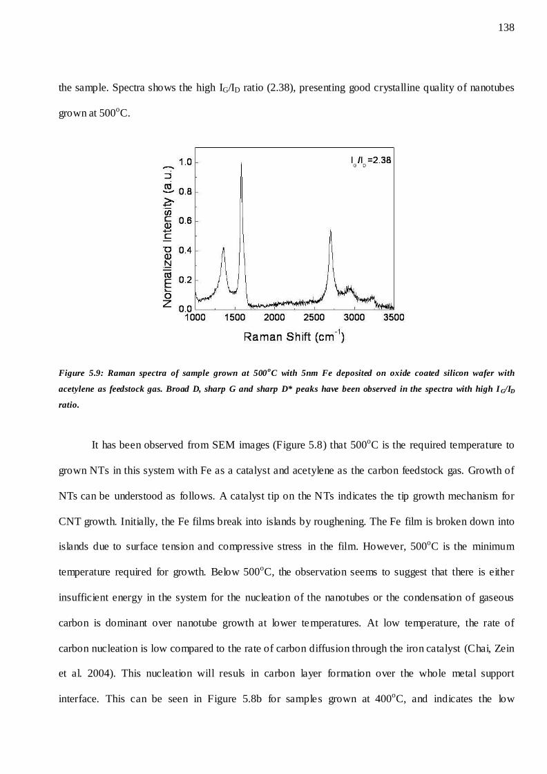
138
the sample. Spectra shows the high IG/ID ratio (2.38), presenting good crystalline quality of nanotubes
grown at 500oC.
Figure 5.9: Raman spectra of sample grown at 500oC with 5nm Fe deposited on oxide coated silicon wafer with
acetylene as feedstock gas. Broad D, sharp G and sharp D* peaks have been observed in the spectra with high I G/ID
ratio.
It has been observed from SEM images (Figure 5.8) that 500oC is the required temperature to
grown NTs in this system with Fe as a catalyst and acetylene as the carbon feedstock gas. Growth of
NTs can be understood as follows. A catalyst tip on the NTs indicates the tip growth mechanism for
CNT growth. Initially, the Fe films break into islands by roughening. The Fe film is broken down into
islands due to surface tension and compressive stress in the film. However, 500oC is the minimum
temperature required for growth. Below 500oC, the observation seems to suggest that there is either
insufficient energy in the system for the nucleation of the nanotubes or the condensation of gaseous
carbon is dominant over nanotube growth at lower temperatures. At low temperature, the rate of
carbon nucleation is low compared to the rate of carbon diffusion through the iron catalyst (Chai, Zein
et al. 2004). This nucleation will resuls in carbon layer formation over the whole metal support
interface. This can be seen in Figure 5.8b for samples grown at 400oC, and indicates the low
139
temperature the CNT growth. At high temperature, the carbon nucleation is much faster than carbon
diffusion through the iron, resulting in the growth of CNTs at 500oC (Figure 5.8c).
Acetylene decomposes easily at 500oC due to its lower decomposition temperature.
Researchers have reported growth of CNTs with acetylene at low temperatures such as 500oC. Growth
in our system can be seen at or higher than 500oC which is in agreement with the work reported by
others (Chen 2005). Catalytic decomposition of acetylene provides the carbon feedstock. The carbon
diffuses onto the island. The diffusion is likely to be surface based rather than through the bulk of the
iron particle due to the lower activation energy of the carbon surface diffusion compared to that of
bulk diffusion. The surface diffusion of carbon then lifts the island as the growth proceeds. As the
temperature increases more carbon will diffuse onto the island due to the higher deco mposition rate at
higher temperature which in turn will give some amorphous carbon formation along with CNT growth
on the sample. Successful growth of CNTs with iron catalyst have been performed at 500oC with
acetylene as the feed stock gas. In this chapter we will refer to these CNTs as CNTacetelyne. Similar
growth parameters will be used to grow CNTs on silicon nanopillars with iron deposited on the tips to
grow Si/C heterojunctions.
5.3 Electrical Characterization of CNTs
The electrical properties of the grown CNTs are explained in this section. For this purpose,
field-effect transistors with CNT channels have been prepared in a similar manner to the SiNW-FET
described in Chapter 4. 300 nm SiO2 deposited on a highly doped p type Si(100) wafer was used for
device fabrication with the Si wafer used as the gate electrode. Interdigital electrodes of Cr (10 nm)/Au
(80 nm) were formed on the SiO2 layer using conventional photolithography and etching techniques.
Detail of these techniques can be found in Chapter 3. The channel length of the electrodes used in this
study was 2.5 µm, 5 µm and 10 µm. Fingers in interdigital structures for source and drain contacts
were connected to the micro sized contact pads. Au as an electrode material was chosen due to its
140
work function and ease of high quality deposition. CNTmethane and CNTacetelyne were sonicated off the
substrates in IPA. Solutions were then drop cast on the above mentioned pre patterned electrode
structures. The device was heated at 100oC for 10 minutes to remove the solvent. Measurements have
been done to understand the electrical properties of these CNTs.
The Keithly 4200 electrometer, which was used to perform electrical current-voltage
measurements for the nanowires were connected through the micro-probes to the source and drain
contact pads. Current versus bias voltage (I-V) measurements were conducted on the samples to
evaluate the electrical properties of the grown NTs. The CNT was considered the main conducting
channel in these devices. The device resistance was calculated for both sets of samples.
Figure 5.10 presents the I-V curves of individual CNTmethane and CNTacetelyne TFTs with the
channel length varied from 2.5 to 10 µm on the normal scale (Figure 5.10 a and c) and on a Log10 scale
(Figure 5.10 b and d). The nanotube channels were found to be conducting. The I-V curves (Figure
5.10 a and c) are non linear, which indicates the presence of a potential barrier. The current increases
rapidly with decreasing channel length. When plotting the curve on a logarithmic scale (Figure 5.10 b
and d), a change in the slope of the current is clearly observed. The high bias regime varies almost
exponentially up to ±1 Volts, suggesting thermionic emission above the potential barrier. At low bias,
tunneling across the barrier occurs. It may be possible that the bias voltage modulates the barrier
width.
The resistance measured for CNTmethane for the 2.5 µm channel was 1.04 MΩ, for 5 µm was
1.76 MΩ and for 10 µm was 3.70 MΩ. The resistance increased with decreasing channel length and
the minimum value obtained was 1.04 MΩ for 2.5 µm channel length. The diameter of the dropped
CNTs were 40 nm and the conducting length of CNTs was the channel length. Using these
measurements, resistivity values were calculated for all sets of data. The resistivity of the CNTmethane
for the 2.5 µm channel was 5.22×10⁻² Ω-cm, for 5 µm was 4.41×10⁻² Ω-cm and for 10 µm was
4.64×10⁻² Ω-cm.
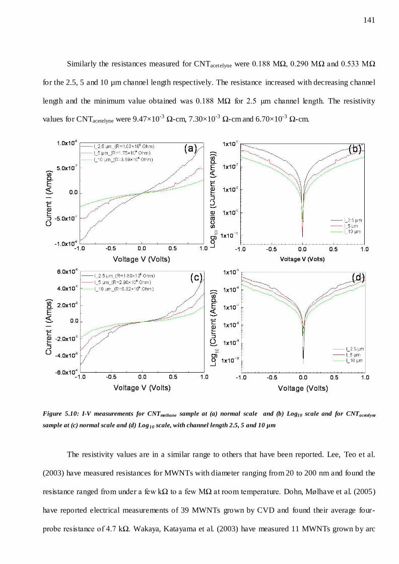
141
Similarly the resistances measured for CNTacetelyne were 0.188 MΩ, 0.290 MΩ and 0.533 MΩ
for the 2.5, 5 and 10 µm channel length respectively. The resistance increased with decreasing channel
length and the minimum value obtained was 0.188 MΩ for 2.5 µm channel length. The resistivity
values for CNTacetelyne were 9.47×10⁻³ Ω-cm, 7.30×10⁻³ Ω-cm and 6.70×10⁻³ Ω-cm.
Figure 5.10: I-V measurements for CNTmethane sample at (a) normal scale and (b) Log10 scale and for CNTacetelyne
sample at (c) normal scale and (d) Log10 scale, with channel length 2.5, 5 and 10 µm
The resistivity values are in a similar range to others that have been reported. Lee, Teo et al.
(2003) have measured resistances for MWNTs with diameter ranging from 20 to 200 nm and found the
resistance ranged from under a few kΩ to a few MΩ at room temperature. Dohn, Mølhave et al. (2005)
have reported electrical measurements of 39 MWNTs grown by CVD and found their average four-
probe resistance of 4.7 kΩ. Wakaya, Katayama et al. (2003) have measured 11 MWNTs grown by arc
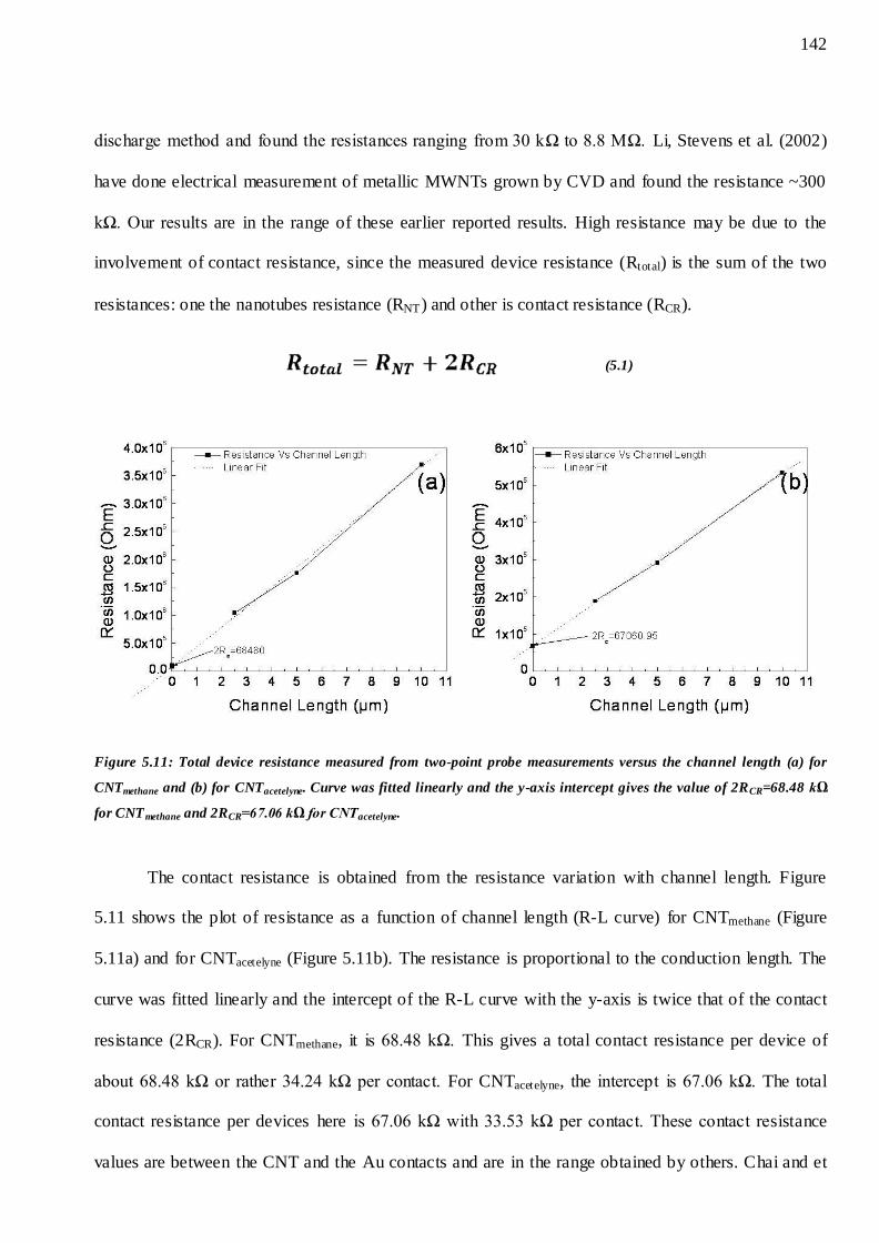
142
discharge method and found the resistances ranging from 30 kΩ to 8.8 MΩ. Li, Stevens et al. (2002)
have done electrical measurement of metallic MWNTs grown by CVD and found the resistance ~300
kΩ. Our results are in the range of these earlier reported results. High resistance may be due to the
involvement of contact resistance, since the measured device resistance (Rtotal) is the sum of the two
resistances: one the nanotubes resistance (RNT) and other is contact resistance (RCR).
(5.1)
Figure 5.11: Total device resistance measured from two-point probe measurements versus the channel length (a) for
CNTmethane and (b) for CNTacetelyne. Curve was fitted linearly and the y-axis intercept gives the value of 2RCR=68.48 kΩ
for CNTmethane and 2RCR=67.06 kΩ for CNTacetelyne.
The contact resistance is obtained from the resistance variation with channel length. Figure
5.11 shows the plot of resistance as a function of channel length (R-L curve) for CNTmethane (Figure
5.11a) and for CNTacetelyne (Figure 5.11b). The resistance is proportional to the conduction length. The
curve was fitted linearly and the intercept of the R-L curve with the y-axis is twice that of the contact
resistance (2RCR). For CNTmethane, it is 68.48 kΩ. This gives a total contact resistance per device of
about 68.48 kΩ or rather 34.24 kΩ per contact. For CNTacetelyne, the intercept is 67.06 kΩ. The total
contact resistance per devices here is 67.06 kΩ with 33.53 kΩ per contact. These contact resistance
values are between the CNT and the Au contacts and are in the range obtained by others. Chai and et
143
al. (2010) have done the electrical characterization of CNTs deposited on Au electrodes and measured
a contact resistance of 8859 Ω. Similarly Kanda, Ootuka et al. (2001) have measured contact resistance
for MWNT/Au for 13 devices and obtained the value ranges for 6.5 to 28 kΩ. An and Friedrich (2011)
have measured contact resistances for MWNTs/Au using electrical contact with focused ion beam. The
measured contact resistance of MWNTs with Au was around 100 kΩ μm. They varied the contact
resistance by changing the contact configurations and obtained values as low as 50 KΩ. Contact
resistances can be reduced by changing the metal electrode.
5.4 Conclusions
In conclusions, CNTs have been successfully grown at 900oC with Ni catalyst using methane
as the carbon feedstock. The effect of nickel thickness, growth temperature, pre-treatment and growth
pressure have been analyzed with SEM images and Raman spectra. Optimum growth for these CNTs
was achieved with 2 nm Ni thickness, 25 minutes pre-treatment time, 100 mbar pressure and a 900oC
growth temperature. CNTs with acetylene as the carbon feedstock have been successfully grown with
5 nm Fe catalyst at 500oC at a pressure of 2 Torr. Samples were analyzed with SEM and Raman
spectra. Both types of CNTs have shown broad D-peak, sharp G-peak and sharp D*-peak in their
Raman spectra with high IG/ID value, indicating good crystallinity of NTs. Electrical measurements
have been done for both type of CNTs. Device resistances measured for CNTmethane was 1.04 MΩ for a
2.5 µm channel length and for CNTacetelyne was 0.188 MΩ for 2.5 µm channel length. These values are
in the range of earlier reported results. Device resistance values are the combination of CNT resistance
and contact resistance. The contact resistance has been calculated from the resitance variation with
channel length and the value of the contact resistance was found to be 68.48 kΩ for CNTmethane and
67.06 kΩ for CNTacetelyne.
144
6 SiNW/CNT heterojunction Growth & Characterisation
We have grown SiNWs through the Bottom-up approach as well as the Top-down approach
followed by CNT growth through the located metal catalyst on the tip of the nanowires. Optimum
growth conditions for silicon nanowires have been achieved to synthesize them on large area with low
cost. These growth conditions have been discussed in Chapter 4. Similarly, carbon nanotube growth in
our systems have been achieved and analyzed, and discussed in Chapter 5. We have used these
conditions to grow heterojunctions of Si/C. In this chapter we will discuss the growth of HJs through
these conditions. A set of experiments were designed to produce Si/C heterojunctions using the
―common catalyst‖ technique. The experimental procedures for this are described in this chapter. For a
better understanding of growth of HJs through the bottom-up approach and top-down approach for
SiNWs, we divide the growth section in to two parts: Bottom-up approach and Top-down approach.
6.1 Bottom-up Approach
After growing seedbed structures via sputtering, they were transferred into the quartz tube
lenton furnace for further annealing and growth of SiNWs and CNTs. The different annealing
conditions used for the growth are discussed below. Thermal annealing was carried out in a vacuum
tube-furnace evacuated to a base pressure of 1.1×10⁻² mbar using a rotary pump. Our best SiNW
growth conditions have been used to grow SiNW, which have been analyzed and subsequent CNT
growth carried out on the same sample.
6.1.1 Optimum conditions for SiNW growth
SiNWs were grown at 1000oC in a tube furnace through thermal annealing. The samples used
in the experiment were Ni/Ti/Si with thicknesses of 20 nm Ni and 100 nm Ti. Ni and Ti were
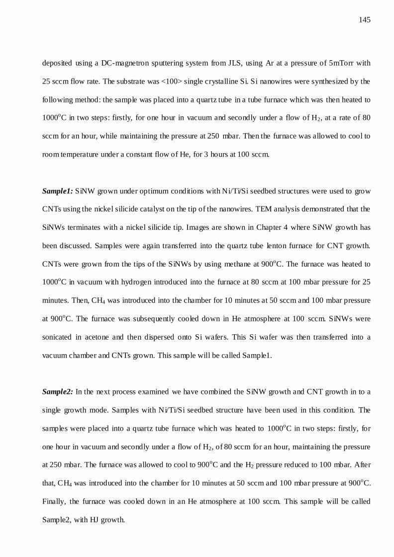
145
deposited using a DC-magnetron sputtering system from JLS, using Ar at a pressure of 5mTorr with
25 sccm flow rate. The substrate was <100> single crystalline Si. Si nanowires were synthesized by the
following method: the sample was placed into a quartz tube in a tube furnace which was then heated to
1000oC in two steps: firstly, for one hour in vacuum and secondly under a flow of H2, at a rate of 80
sccm for an hour, while maintaining the pressure at 250 mbar. Then the furnace was allowed to cool to
room temperature under a constant flow of He, for 3 hours at 100 sccm.
Sample1: SiNW grown under optimum conditions with Ni/Ti/Si seedbed structures were used to grow
CNTs using the nickel silicide catalyst on the tip of the nanowires. TEM analysis demonstrated that the
SiNWs terminates with a nickel silicide tip. Images are shown in Chapter 4 where SiNW growth has
been discussed. Samples were again transferred into the quartz tube lenton furnace for CNT growth.
CNTs were grown from the tips of the SiNWs by using methane at 900oC. The furnace was heated to
1000oC in vacuum with hydrogen introduced into the furnace at 80 sccm at 100 mbar pressure for 25
minutes. Then, CH4 was introduced into the chamber for 10 minutes at 50 sccm and 100 mbar pressure
at 900oC. The furnace was subsequently cooled down in He atmosphere at 100 sccm. SiNWs were
sonicated in acetone and then dispersed onto Si wafers. This Si wafer was then transferred into a
vacuum chamber and CNTs grown. This sample will be called Sample1.
Sample2: In the next process examined we have combined the SiNW growth and CNT growth in to a
single growth mode. Samples with Ni/Ti/Si seedbed structure have been used in this condition. The
samples were placed into a quartz tube furnace which was heated to 1000oC in two steps: firstly, for
one hour in vacuum and secondly under a flow of H2, of 80 sccm for an hour, maintaining the pressure
at 250 mbar. The furnace was allowed to cool to 900oC and the H2 pressure reduced to 100 mbar. After
that, CH4 was introduced into the chamber for 10 minutes at 50 sccm and 100 mbar pressure at 900oC.
Finally, the furnace was cooled down in an He atmosphere at 100 sccm. This sample will be called
Sample2, with HJ growth.
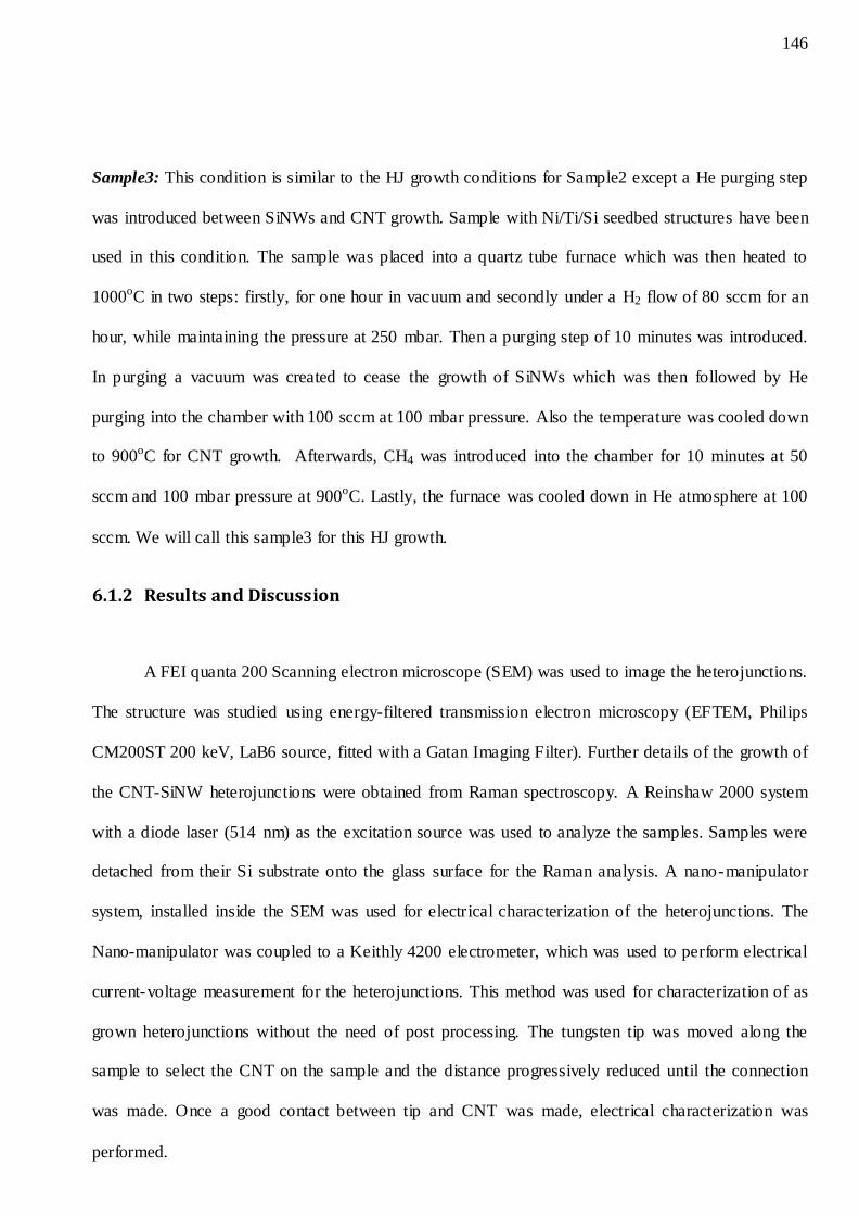
146
Sample3: This condition is similar to the HJ growth conditions for Sample2 except a He purging step
was introduced between SiNWs and CNT growth. Sample with Ni/Ti/Si seedbed structures have been
used in this condition. The sample was placed into a quartz tube furnace which was then heated to
1000oC in two steps: firstly, for one hour in vacuum and secondly under a H2 flow of 80 sccm for an
hour, while maintaining the pressure at 250 mbar. Then a purging step of 10 minutes was introduced.
In purging a vacuum was created to cease the growth of SiNWs which was then followed by He
purging into the chamber with 100 sccm at 100 mbar pressure. Also the temperature was cooled down
to 900oC for CNT growth. Afterwards, CH4 was introduced into the chamber for 10 minutes at 50
sccm and 100 mbar pressure at 900oC. Lastly, the furnace was cooled down in He atmosphere at 100
sccm. We will call this sample3 for this HJ growth.
6.1.2 Results and Discussion
A FEI quanta 200 Scanning electron microscope (SEM) was used to image the heterojunctions.
The structure was studied using energy-filtered transmission electron microscopy (EFTEM, Philips
CM200ST 200 keV, LaB6 source, fitted with a Gatan Imaging Filter). Further details of the growth of
the CNT-SiNW heterojunctions were obtained from Raman spectroscopy. A Reinshaw 2000 system
with a diode laser (514 nm) as the excitation source was used to analyze the samples. Samples were
detached from their Si substrate onto the glass surface for the Raman analysis. A nano-manipulator
system, installed inside the SEM was used for electrical characterization of the heterojunctions. The
Nano-manipulator was coupled to a Keithly 4200 electrometer, which was used to perform electrical
current-voltage measurement for the heterojunctions. This method was used for characterization of as
grown heterojunctions without the need of post processing. The tungsten tip was moved along the
sample to select the CNT on the sample and the distance progressively reduced until the connection
was made. Once a good contact between tip and CNT was made, electrical characterization was
performed.
147
6.1.2.1 Sample1
Figure 6.1: SEM images of (a) SiNWs growth, (b) magnified image of SiNW growth, (c) CNTs growth on SiNWs, (d)
magnified image of CNTs grown on SiNWs, (e) CNTs grown on drop-casted SiNWs on wafer and (f) CNTs grown on
SiNWs, dropped on Si wafer after growth.
148
Figure 6.1 shows the scanning electron microscopy images of the as grown heterojunctions.
Figure 6.1a and Figure 6.1b are images before CNT growth. The images show the high density growth
of SiNWs on the sample. Figure 6.1c and figure 6.1d are images after CNT growth on the same
sample, and shows the growth of nanotubes on SiNW. These CNTs are curly in nature and can be
differentiated from SiNWs which are long and straight. CNTs grown on a dispersed SiNWs solution is
shown in figure 6.1e. It confirms the curly CNT growth on straight SiNWs similar to that in figure
6.1d. Figure 6.1f is the solution drop-cast of HJs on a Si wafer which verify similar HJ growth as
shown in figure 6.1c, figure 6.1d and figure 6.1e.
Figure 6.2: Raman spectra of CNT-SiNW heterojunction (Sample1). Raman signal from CNTs and SiNWs have been
found in the spectra, indicating the presence of CNT and SiNWs on the sample.
Further details of the formation of heterojunctions were obtained from Raman spectroscopy.
Figure 6.2 is the Raman spectra of the CNT-SiNW heterojunctions. Si peaks along with CNT peaks
can be found in the spectra. The Raman spectra of sample1 show prominent Si Raman features at
~514.9 cm-1, with a shoulder at 489.3 cm-1. In addition, there are two broad peaks at ~968.2 and 283
cm-1. When comparing them with the c-Si Raman spectrum, SiNWs show similar bands, exhibiting
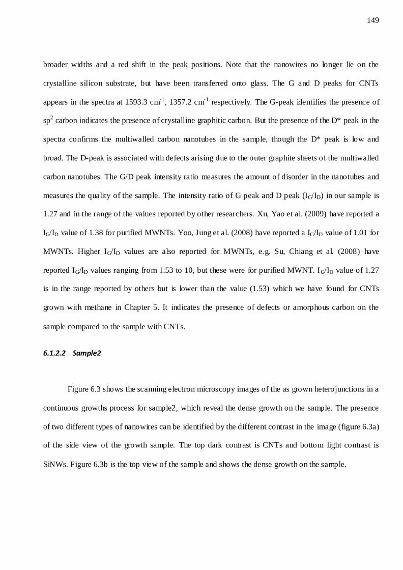
149
broader widths and a red shift in the peak positions. Note that the nanowires no longer lie on the
crystalline silicon substrate, but have been transferred onto glass. The G and D peaks for CNTs
appears in the spectra at 1593.3 cm-1, 1357.2 cm-1 respectively. The G-peak identifies the presence of
sp2 carbon indicates the presence of crystalline graphitic carbon. But the presence of the D* peak in the
spectra confirms the multiwalled carbon nanotubes in the sample, though the D* peak is low and
broad. The D-peak is associated with defects arising due to the outer graphite sheets of the multiwalled
carbon nanotubes. The G/D peak intensity ratio measures the amount of disorder in the nanotubes and
measures the quality of the sample. The intensity ratio of G peak and D peak (IG/ID) in our sample is
1.27 and in the range of the values reported by other researchers. Xu, Yao et al. (2009) have reported a
IG/ID value of 1.38 for purified MWNTs. Yoo, Jung et al. (2008) have reported a IG/ID value of 1.01 for
MWNTs. Higher IG/ID values are also reported for MWNTs, e.g. Su, Chiang et al. (2008) have
reported IG/ID values ranging from 1.53 to 10, but these were for purified MWNT. IG/ID value of 1.27
is in the range reported by others but is lower than the value (1.53) which we have found for CNTs
grown with methane in Chapter 5. It indicates the presence of defects or amorphous carbon on the
sample compared to the sample with CNTs.
6.1.2.2 Sample2
Figure 6.3 shows the scanning electron microscopy images of the as grown heterojunctions in a
continuous growths process for sample2, which reveal the dense growth on the sample. The presence
of two different types of nanowires can be identified by the different contrast in the image (figure 6.3a)
of the side view of the growth sample. The top dark contrast is CNTs and bottom light contrast is
SiNWs. Figure 6.3b is the top view of the sample and shows the dense growth on the sample.
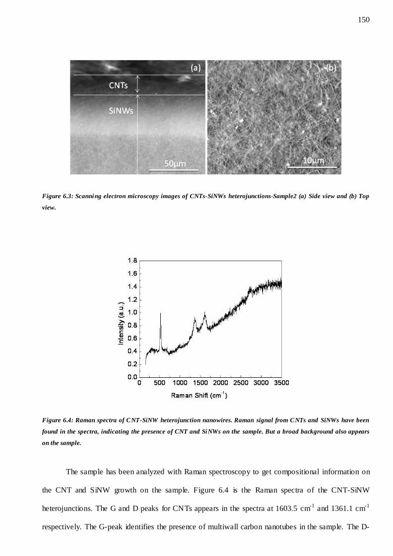
150
Figure 6.3: Scanning electron microscopy images of CNTs-SiNWs heterojunctions-Sample2 (a) Side view and (b) Top
view.
Figure 6.4: Raman spectra of CNT-SiNW heterojunction nanowires. Raman signal from CNTs and SiNWs have been
found in the spectra, indicating the presence of CNT and SiNWs on the sample. But a broad background also appears
on the sample.
The sample has been analyzed with Raman spectroscopy to get compositional information on
the CNT and SiNW growth on the sample. Figure 6.4 is the Raman spectra of the CNT-SiNW
heterojunctions. The G and D peaks for CNTs appears in the spectra at 1603.5 cm-1 and 1361.1 cm-1
respectively. The G-peak identifies the presence of multiwall carbon nanotubes in the sample. The D-
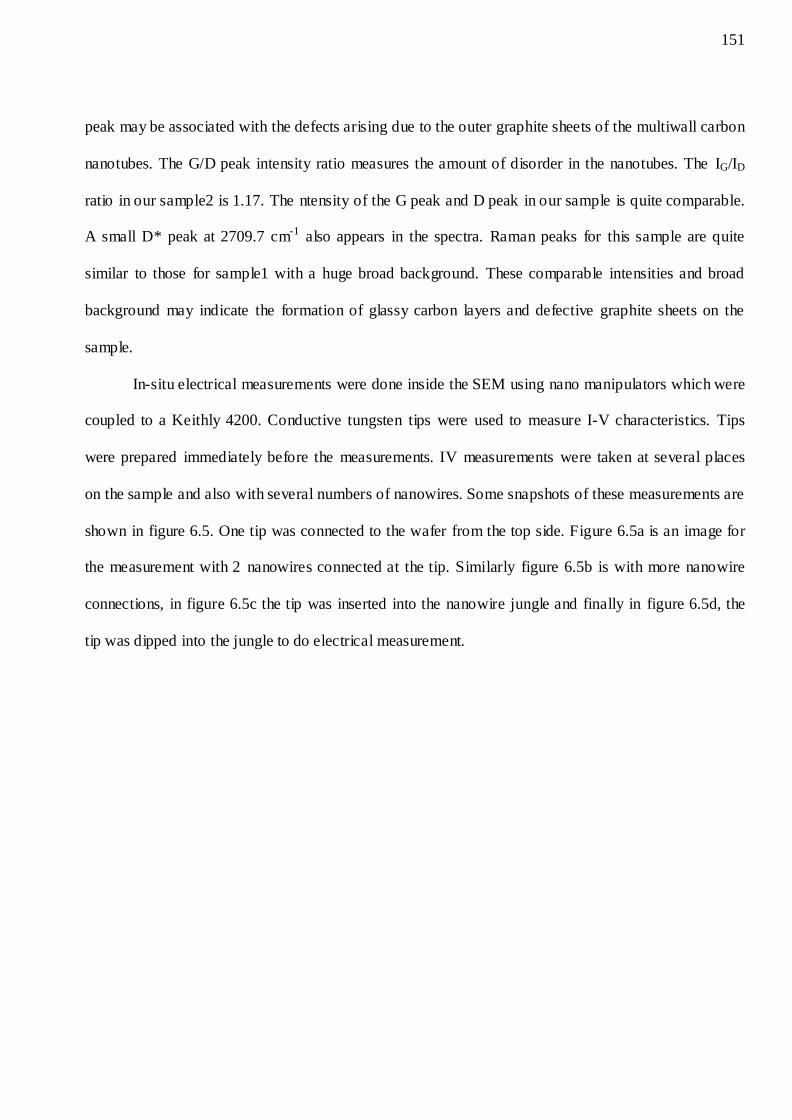
151
peak may be associated with the defects arising due to the outer graphite sheets of the multiwall carbon
nanotubes. The G/D peak intensity ratio measures the amount of disorder in the nanotubes. The IG/ID
ratio in our sample2 is 1.17. The ntensity of the G peak and D peak in our sample is quite comparable.
A small D* peak at 2709.7 cm-1 also appears in the spectra. Raman peaks for this sample are quite
similar to those for sample1 with a huge broad background. These comparable intensities and broad
background may indicate the formation of glassy carbon layers and defective graphite sheets on the
sample.
In-situ electrical measurements were done inside the SEM using nano manipulators which were
coupled to a Keithly 4200. Conductive tungsten tips were used to measure I-V characteristics. Tips
were prepared immediately before the measurements. IV measurements were taken at several places
on the sample and also with several numbers of nanowires. Some snapshots of these measurements are
shown in figure 6.5. One tip was connected to the wafer from the top side. Figure 6.5a is an image for
the measurement with 2 nanowires connected at the tip. Similarly figure 6.5b is with more nanowire
connections, in figure 6.5c the tip was inserted into the nanowire jungle and finally in figure 6.5d, the
tip was dipped into the jungle to do electrical measurement.
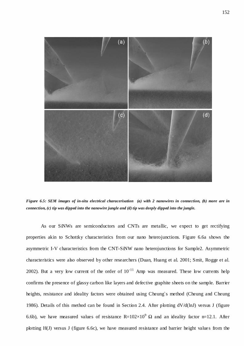
152
Figure 6.5: SEM images of in-situ electrical characerisation (a) with 2 nanowires in connection, (b) more are in
connection, (c) tip was dipped into the nanowire jungle and (d) tip was deeply dipped into the jungle.
As our SiNWs are semiconductors and CNTs are metallic, we expect to get rectifying
properties akin to Schottky characteristics from our nano heterojunctions. Figure 6.6a shows the
asymmetric I-V characteristics from the CNT-SiNW nano heterojunctions for Sample2. Asymmetric
characteristics were also observed by other researchers (Duan, Huang et al. 2001; Smit, Rogge et al.
2002). But a very low current of the order of 10-11 Amp was measured. These low currents help
confirms the presence of glassy carbon like layers and defective graphite sheets on the sample. Barrier
heights, resistance and ideality factors were obtained using Cheung`s method (Cheung and Cheung
1986). Details of this method can be found in Section 2.4. After plotting dV/d(lnJ) versus J (figure
6.6b), we have measured values of resistance R=102×109 Ω and an ideality factor n=12.1. After
plotting H(J) versus J (figure 6.6c), we have measured resistance and barrier height values from the
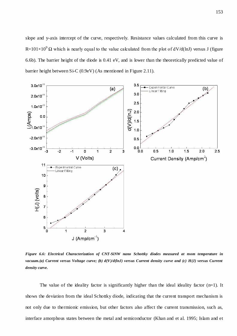
153
slope and y-axis intercept of the curve, respectively. Resistance values calculated from this curve is
R=101×109 Ω which is nearly equal to the value calculated from the plot of dV/d(lnJ) versus J (figure
6.6b). The barrier height of the diode is 0.41 eV, and is lower than the theoretically predicted value of
barrier height between Si-C (0.9eV) (As mentioned in Figure 2.11).
Figure 6.6: Electrical Characterization of CNT-SiNW nano Schottky diodes measured at room temperature in
vacuum.(a) Current versus Voltage curve; (b) d(V)/d(lnJ) versus Current density curve and (c) H(J) versus Current
density curve.
The value of the ideality factor is significantly higher than the ideal ideality factor (n=1). It
shows the deviation from the ideal Schottky diode, indicating that the current transport mechanism is
not only due to thermionic emission, but other factors also affect the current transmission, such as,
interface amorphous states between the metal and semiconductor (Khan and et al. 1995; Islam and et
154
al. 2011), tunneling current, in highly doped semiconductors (Sze 1981; Zhang, Yao et al. 2007), and
generation-recombination current. Cobas (Cobas 2010) have studied the transport properties of carbon
nanotubes and reported the ideality factor ranges from 2 to 20. They have attributed this to the high
tunneling current at the metal-semiconductor contact. Mohammad (Mohammad 2010) studied the 1D
rectifying contacts and reported that the ideality factor can reach up to 20 for metal-semiconductor
nanowire Schottky junctions. The high value of ideality factor is due to the temperature effect,
tunneling current and interfacial states. We attribute the high value of ideality factor in our HJs to the
interfacial amorphous layer and tunneling current. An amorphous layer was formed during the growth
itself. Raman spectra also verified this by a broad background in Raman spectra. It resulted in the high
resistance and high ideality value in this HJ. A high D peak intensity indicates the presence of defects
in the HJs. These are responsible for the tunneling current and will contribute to increasing the ideality
factor.
6.1.2.3 Sample3
To get better conductivity of the heterojunctions, a purging step was introduced in the growth
process with Sample3. Figure 6.7 shows the scanning electron microscopy images of the as grown
heterojunctions which reveals dense growth on the sample. Figure 6.7a is a side view of the sample
indicating the presence of two different types of nanowires by visible differences in the contrast. The
top bright contrast is CNTs and bottom light contrast is SiNWs. While Figure 6.7b is a top view of
sample showing a dense growth on the sample.
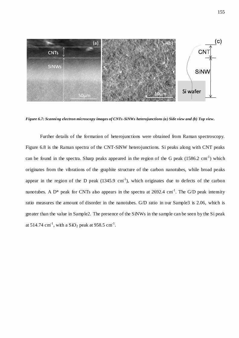
155
Figure 6.7: Scanning electron microscopy images of CNTs-SiNWs heterojunctions (a ) Side view and (b) Top view.
Further details of the formation of heterojunctions were obtained from Raman spectroscopy.
Figure 6.8 is the Raman spectra of the CNT-SiNW heterojunctions. Si peaks along with CNT peaks
can be found in the spectra. Sharp peaks appeared in the region of the G peak (1586.2 cm-1) which
originates from the vibrations of the graphite structure of the carbon nanotubes, while broad peaks
appear in the region of the D peak (1345.9 cm-1), which originates due to defects of the carbon
nanotubes. A D* peak for CNTs also appears in the spectra at 2692.4 cm-1. The G/D peak intensity
ratio measures the amount of disorder in the nanotubes. G/D ratio in our Sample3 is 2.06, which is
greater than the value in Sample2. The presence of the SiNWs in the sample can be seen by the Si peak
at 514.74 cm-1, with a SiO2 peak at 958.5 cm-1.
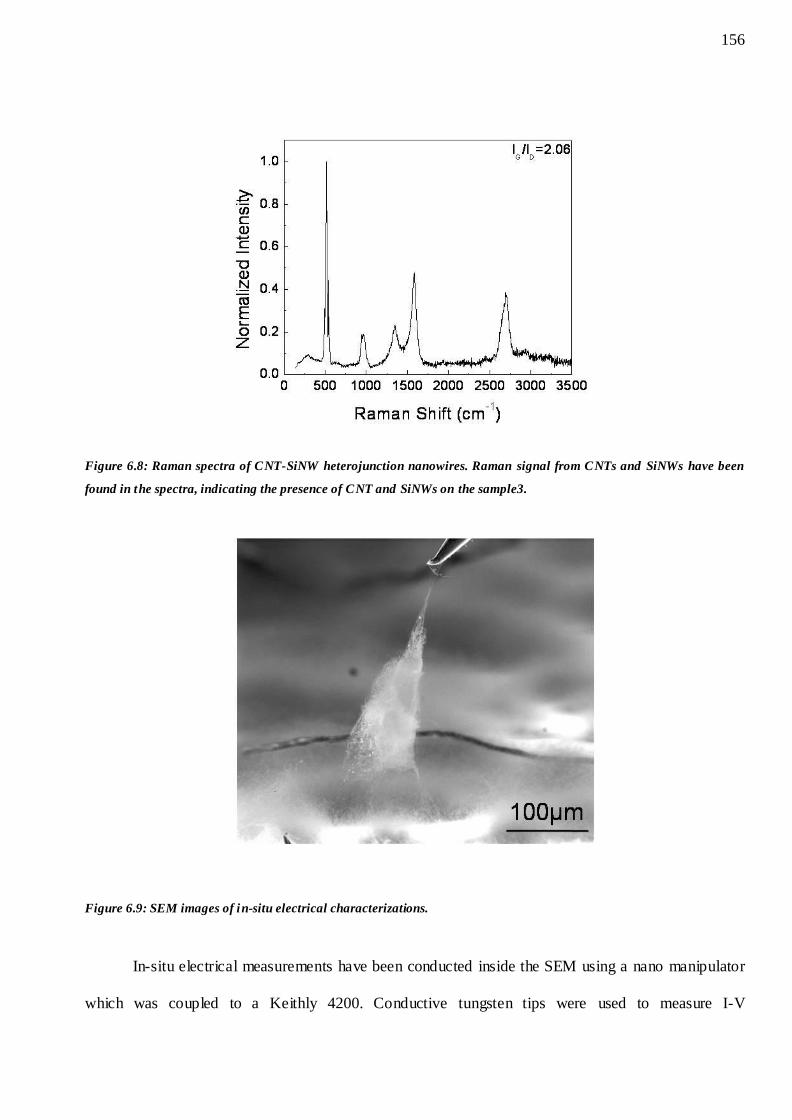
156
Figure 6.8: Raman spectra of CNT-SiNW heterojunction nanowires. Raman signal from CNTs and SiNWs have been
found in the spectra, indicating the presence of CNT and SiNWs on the sample3.
Figure 6.9: SEM images of in-situ electrical characterizations.
In-situ electrical measurements have been conducted inside the SEM using a nano manipulator
which was coupled to a Keithly 4200. Conductive tungsten tips were used to measure I-V
157
characteristics. Tips were prepared immediately before the measurements. Figure 6.9 shows an image
taken during the measurement.
Assuming our SiNWs are semiconductors and CNTs are metallic we expect to get Schottky
characteristics from our nano heterojunctions. Figure 6.10a shows the I-V characteristics from the
CNT-SiNW nano heterojunctions which are asymmetric and rectify at low reverse bias voltage.
Typical Schottky diode characteristics can be observed in the forward bias condition while it
shows rectifying characteristics at low reverse bias. This type of reverse characteristics has been
reported for nano Schottky diodes (Yang, Meng et al. 2007; Shafiei, Yu et al. 2010). Ideally, Schottky
diodes are explained using thermionic emission theory (Sze 1981) according to which reverse current
in Schottky diodes are almost zero or in the range of nA, with diodes considered as `off` in reverse bias
conditions. But in nano heterojunctions, where the current is of the order of nA, we cannot neglect the
reverse current in Schottky diodes. For calculating barrier heights, resistance and ideality factor, we
use Cheung`s method (Cheung and Cheung 1986). After plotting dV/d(lnJ) versus J (fig10b), we have
measured value of resistance of R=577 kΩ and an ideality factor n=1.26. After plotting H(I) versus I
(fig10c), we have measured resistance and barrier height value from the slope and y-axis intercept of
the curve respectively. The resistance value calculated from this curve is 553 kΩ which is near to the
value calculated from the data in figure 6.10b. The barrier height of the diode is 0.24 eV which is
lower than the theoretically predicted value of barrier height between Si-C (0.9 eV) (As mentioned
Figure 2.11). The value of ideality factor is higher than the ideal ideality factor (n=1).
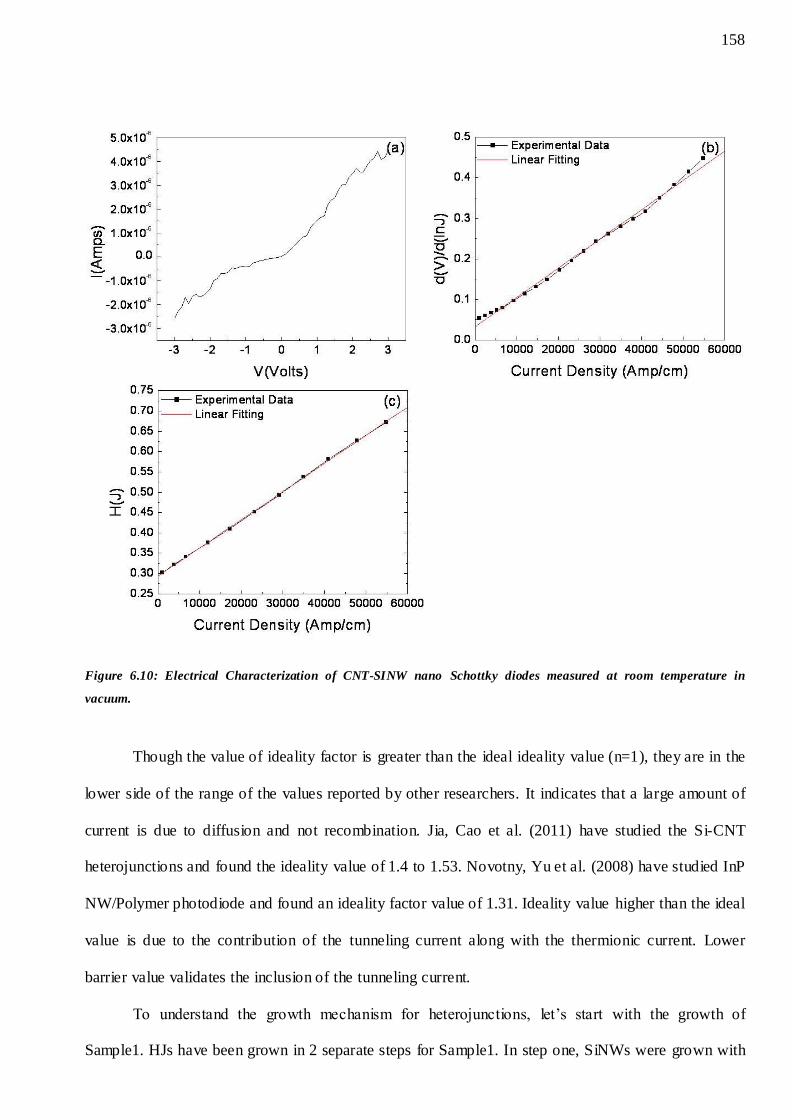
158
Figure 6.10: Electrical Characterization of CNT-SINW nano Schottky diodes measured at room temperature in
vacuum.
Though the value of ideality factor is greater than the ideal ideality value (n=1), they are in the
lower side of the range of the values reported by other researchers. It indicates that a large amount of
current is due to diffusion and not recombination. Jia, Cao et al. (2011) have studied the Si-CNT
heterojunctions and found the ideality value of 1.4 to 1.53. Novotny, Yu et al. (2008) have studied InP
NW/Polymer photodiode and found an ideality factor value of 1.31. Ideality value higher than the ideal
value is due to the contribution of the tunneling current along with the thermionic current. Lower
barrier value validates the inclusion of the tunneling current.
To understand the growth mechanism for heterojunctions, let‘s start with the growth of
Sample1. HJs have been grown in 2 separate steps for Sample1. In step one, SiNWs were grown with
159
Ni/Ti/Si seedbed structures, and then the sample taken from the vacuum chamber for analyzing. After
analysis, samples were again transferred into the vacuum chamber for CNT growth. The growth
mechanism for SiNWs has been reported in Chapter 4, where a combination of SLS and VLS
mechanism has been used to explain the SiNW growth in our chamber. These grown SiNWs have
nickel silicide at the tip of the nanowires which acts as a catalyst for CNT growth. After transferring
the SiNW sample again into the chamber, temperature is increased to 900oC and kept at the same
temperature in an H2 atmosphere. H2 will activate the catalyst tip of the nanowires by reducing the
oxidized catalyst particle which may have oxidized during the exposure to the environment which took
place during the analysis of the SiNWs. When CH4 is introduced into the tube, it easily decomposes at
900oC and the H2 helps to reduce the decomposition of methane for reducing the excess deposition of
carbon at the catalyst which may interfere with the CNT growth. Decomposition of methane facilitates
the CNT growth through a base growth mechanism. At high temperature, a catalytic head will embed
into the nanowire tip which will promote the base growth of carbon nanotubes. CNT growth with the
base growth mechanism at higher temperature has been observed by other researchers (Esconjauregui
and et al. 2008; Ohashi and et al. 2008).
During the continuous growth of HJs in the furnace for Sample2, SiNW growth started in a
similar to Sample1 by a combined SLS and VLS growth mechanism through the decomposition of
SiO. After an hour of H2 flow into the chamber for SiNW growth, when methane was introduced into
the chamber a different mechanism takes place, as there is already SiO vapour present, which changes
the chemistry and influences the growth process. The gas phase reaction between SiO with CH4 will
provide SiC according to the following equation (Setiowati and Kimura 1997)
( 6.1)
This SiC may react with the oxide clad of the SiNW (Note that SiNWs grown from this process
have Si core and Oxide cladding according to the following equation (Borisov and Yudin 1968)
160
( 6.2)
The presence of CO in the furnace will enhance the carbon diffusion onto the catalyst and will
change the ratio of C and H which will affect the crystalline structure of the grown nanotubes. Zhang
and Smith (2002) have observed a similar effect of CO on the CH4. Absence of SiO2 peaks in the
Raman spectra of Sample2 shows the physical absence of SiO2 compared to Sample1. It may have
been reduced from SiC according to equation 6.2. The broad background in the Raman spectra of
Sample2 and high resistance in electrical characterization of Sample2 supports the decrease in the
crystalline nature of carbon nanotubes which may be due to the change in the ratio of C and H in the
furnace.
When the purging step was introduced into the growth, an increase in crystalline nature of
CNTs and the presence of the SiO2 peak was observed for Sample3 (Figure 6.9). In the purging step,
the furnace was pumped down after SiNW growth and He was introduced into the furnace. Pumping
down will help to get rid of the existing SiO in the chamber which is present during the SiNW growth.
Then, methane was introduced for CNT growth and decomposition of methane facilitate s CNT growth
within the VLS mechanism.
6.2 Top-down Approach
6.2.1 Experimental Conditions
Metal assisted silicon etching has been employed for SiNW fabrication. The best aspect ratio
and most regular morphologies have been obtained by using Au nano dots as a mask for etching. P-Si
wafers were initially cleaned with the 3 step process and 20 nm Au was deposited using the JLS
sputterer in an Ar atmosphere on to the wafer. The films were then subsequently annealed in the
Lenton furnace for 30 minutes in a He atmosphere at 300oC. The furnace was cooled down to room
temperature and substrates taken out for Si etching. The substrate with Au metal nano dots were then
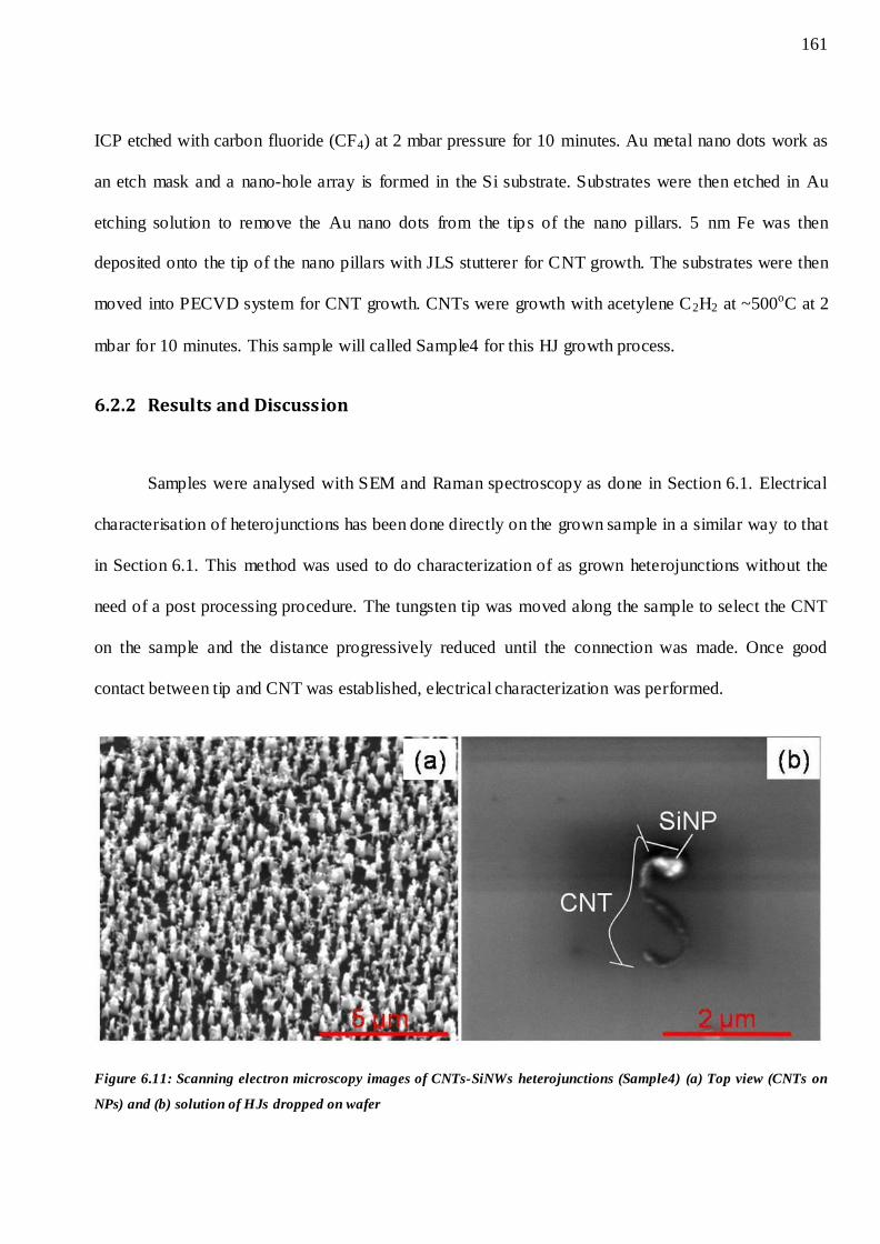
161
ICP etched with carbon fluoride (CF4) at 2 mbar pressure for 10 minutes. Au metal nano dots work as
an etch mask and a nano-hole array is formed in the Si substrate. Substrates were then etched in Au
etching solution to remove the Au nano dots from the tips of the nano pillars. 5 nm Fe was then
deposited onto the tip of the nano pillars with JLS stutterer for CNT growth. The substrates were then
moved into PECVD system for CNT growth. CNTs were growth with acetylene C2H2 at ~500oC at 2
mbar for 10 minutes. This sample will called Sample4 for this HJ growth process.
6.2.2 Results and Discussion
Samples were analysed with SEM and Raman spectroscopy as done in Section 6.1. Electrical
characterisation of heterojunctions has been done directly on the grown sample in a similar way to that
in Section 6.1. This method was used to do characterization of as grown heterojunctions without the
need of a post processing procedure. The tungsten tip was moved along the sample to select the CNT
on the sample and the distance progressively reduced until the connection was made. Once good
contact between tip and CNT was established, electrical characterization was performed.
Figure 6.11: Scanning electron microscopy images of CNTs-SiNWs heterojunctions (Sample4) (a) Top view (CNTs on
NPs) and (b) solution of HJs dropped on wafer
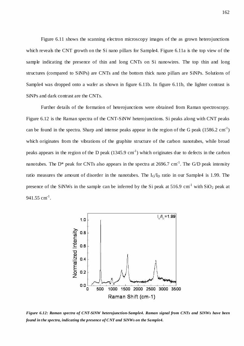
162
Figure 6.11 shows the scanning electron microscopy images of the as grown heterojunctions
which reveals the CNT growth on the Si nano pillars for Sample4. Figure 6.11a is the top view of the
sample indicating the presence of thin and long CNTs on Si nanowires. The top thin and long
structures (compared to SiNPs) are CNTs and the bottom thick nano pillars are SiNPs. Solutions of
Sample4 was dropped onto a wafer as shown in figure 6.11b. In figure 6.11b, the lighter contrast is
SiNPs and dark contrast are the CNTs.
Further details of the formation of heterojunctions were obtained from Raman spectroscopy.
Figure 6.12 is the Raman spectra of the CNT-SiNW heterojunctions. Si peaks along with CNT peaks
can be found in the spectra. Sharp and intense peaks appear in the region of the G peak (1586.2 cm-1)
which originates from the vibrations of the graphite structure of the carbon nanotubes, while broad
peaks appears in the region of the D peak (1345.9 cm-1) which originates due to defects in the carbon
nanotubes. The D* peak for CNTs also appears in the spectra at 2696.7 cm-1. The G/D peak intensity
ratio measures the amount of disorder in the nanotubes. The IG/ID ratio in our Sample4 is 1.99. The
presence of the SiNWs in the sample can be inferred by the Si peak at 516.9 cm-1 with SiO2 peak at
941.55 cm-1.
Figure 6.12: Raman spectra of CNT-SiNW heterojunction-Sample4. Raman signal from CNTs and SiNWs have been
found in the spectra, indicating the presence of CNT and SiNWs on the Sample4.
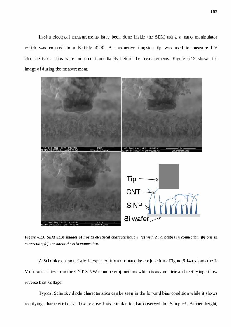
163
In-situ electrical measurements have been done inside the SEM using a nano manipulator
which was coupled to a Keithly 4200. A conductive tungsten tip was used to measure I-V
characteristics. Tips were prepared immediately before the measurements. F igure 6.13 shows the
image of during the measurement.
Figure 6.13: SEM SEM images of in-situ electrical characterization (a) with 2 nanotubes in connection, (b) one in
connection, (c) one nanotube is in connection.
A Schottky characteristic is expected from our nano heterojunctions. Figure 6.14a shows the I-
V characteristics from the CNT-SiNW nano heterojunctions which is asymmetric and rectify ing at low
reverse bias voltage.
Typical Schottky diode characteristics can be seen in the forward bias condition while it shows
rectifying characteristics at low reverse bias, similar to that observed for Sample3. Barrier height,
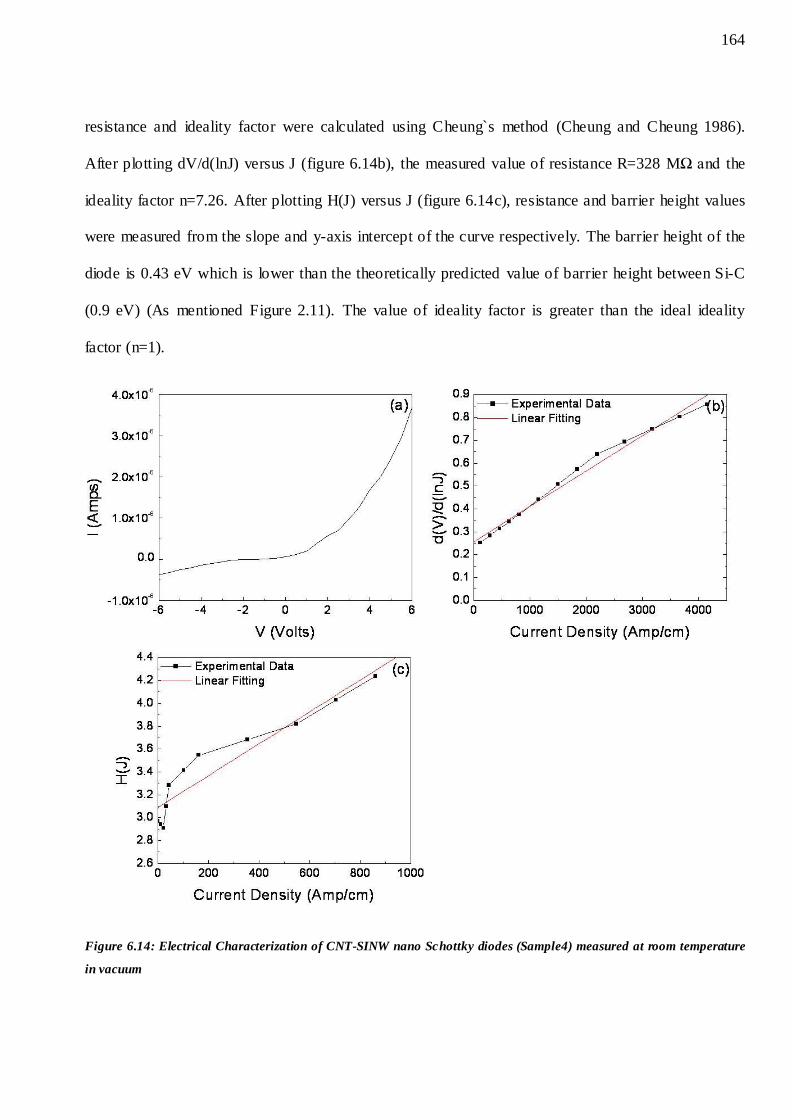
164
resistance and ideality factor were calculated using Cheung`s method (Cheung and Cheung 1986).
After plotting dV/d(lnJ) versus J (figure 6.14b), the measured value of resistance R=328 MΩ and the
ideality factor n=7.26. After plotting H(J) versus J (figure 6.14c), resistance and barrier height values
were measured from the slope and y-axis intercept of the curve respectively. The barrier height of the
diode is 0.43 eV which is lower than the theoretically predicted value of barrier height between Si-C
(0.9 eV) (As mentioned Figure 2.11). The value of ideality factor is greater than the ideal ideality
factor (n=1).
Figure 6.14: Electrical Characterization of CNT-SINW nano Schottky diodes (Sample4) measured at room temperature
in vacuum
165
The value of the barrier height is comparable to the theoretical value reported in the literature.
The value of ideality factor is greater than the ideal ideality factor (n=1). This deviation from ideal
value is attributed due to a possible amorphous layer formed between the surface of the SiNW and
CNT after SiNW formation. An insulating layer will reduce the current transmission probability into
the SiNP from CNT and increase the ideality factor which depends on the current value. It is possible
that the oxidation of nanowires occurs due to exposure to the atmosphere during the movement of the
sample for CNT growth.
6.3 Real Interfaces
Oxidation of SiNWs at higher temperature was the main problem which was faced during the
growth. Initially, optimized conditions for SiNW growth were achieved. Though using nickel silicide
tips, several attempts have been made to grow CNTs on the top of these SiNWs in a second step. But
exposure of SiNWs to the environment oxidized them easily. Also, annealing of SiNWs at higher
temperature in pre-treatment (in second step) for CNT growth, changes them into oxidized SiNWs
which is a hurdle to avoid as SiNWs tended to oxidize at high temperature. SiNW and CNT growth
has been done in a single step to avoid the oxidation of SiNW.
To avoid oxidization of SiNWs during CNT growth, simultaneously, different routes for
fabrication were attempted. Initially CNTs were grown with the method explained in Chapter 5 using
methane. SiNWs were grown on top of CNT, in a similar way to that explained in Chapter 4. Common
catalysts have been used for both growth regimes. As we have seen, SiNWs in our systems was grown
through a combination of SLS and VLS mechanisms. We have used SiO vapour generated from the
Ni/Ti/Si wafer to grow SiNWs on the top of CNTs. Though SiNW growth with SiO vapour on the
sample was successful, it resulted in amorphous carbon layers and removed the feasibility of using this
to grow HJs.
166
A low temperature growth or lower pre treatment time for CNT growth was another possible
solution attempted. The higher cracking temperature of methane made us use alternate carbon
feedstock gas for the growth. Acetylene is a possible carbon source for low temperature CNT growth.
CNT growth with acetylene at low temperature (at 500oC) on SiNWs has been achieved and its results
analyzed. Oxidation of SiNWs was a problem in this experiment, due to exposure of SiNW to the
environment, prior to the CNT growth. Similar CNT growth conditions have been used for Sample4
which is explained in earlier parts of this chapter. When CNT growth was conducted immediately after
SiNWs growth (Sample3), it reduced the pre treatment time and allowed fabricating SiNW-CNT
heterojunctions with rectifying behavior at low reverse voltage.
6.4 Conclusions
The fabrication of heterojunctions of Si/C has been studied in this chapter. A successful growth
of HJs with top-down approach and bottom-up approach was achieved as seen in Sample3 and
Sample4. The Bottom-up approach in Sample3 gave good HJs with low ideality factor 1.26, 553 KΩ
resistance and 0.24 eV barrier height, while Top-down approach gave a 7.26 ideality factor and 328
MΩ resistance. It gave a 0.43 eV barrier height which is comparable to the actual barrier height of the
HJ. HJ growth similar to Sample3 has been done with a Au catalyst also which shows dense growth of
HJs as for Sample3 and Raman spectra for the same sample indicates the presence of CNTs and
SiNWs on the sample with an intense carbon D peak.
167
7 Summary and Conclusions
The aim of this research was to study the carbon nanotubes / silicon nanowires heterojunctions
and to analyze the electronic properties of these HJ with growth of the low cost, large area synthesis of
silicon nanowires. As part of this work, optimized conditions for the growth of crystalline silicon
nanowires and carbon nanotubes have been achieved. These optimum conditions were further used to
synthesize HJs of carbon nanotubes and silicon nanowires. In addition, electrical characterizations for
SiNWs and CNTs have been conducted in this work.
7.1 Silicon Nanowire Growth
Silicon nanowire synthesis has been performed with low cost, suitable for large area devices.
We started with a bottom-up approach to grow silicon nanowires. In this process initially Silica
nanowires have been grown from thermal annealing of Ni/Si, Ni/SiO2/Si and Ni/Ti/SiO2/Si in a
furnace at 1000oC in a He and H2 environment. Nickel acts as catalyst in this growth. The effect of
each layer on the growth has been studied carefully. The grown nanowire diameter can be controlled
by the thickness of the metal layers in the seedbed. A novel method has been developed for the large
scale synthesis of core-clad crystalline silicon nanowires by combining the SLS and VLS growth
mechanism. A detailed calculation based on a phonon confinement model has been performed to
interpret the first order Raman-spectra. The diameter of the nanowires has been calculated with this
model.
Then silicon nanopillars were synthesized by using top-down approach by etching of silicon
wafer. Self-organized metal island formation by low temperature annealing has been found to be a
good solution for low cost nano dot mask formation. An ICP-RIE (STS) system was use to etch Si
with CF4 gas. Prior to the etching of Au array patterned samples, a set of experiments was done to
observe the effect of gas flow rate and gas pressure on etching. A high gas flow rate results in high
168
concentration of fluorine ions with a resultant increase in etch rate, while a high gas pressure will
decrease the mean free path resulting in a decrease in etch rates. A decrease in anisotropy with
increasing gas pressure was also observed. For anisotropic Si etching, the optimum condition of
etching was 30 sccm CF4 flow rate and 2 mTorr gas pressures.
The electrical properties of core-clad crystalline silicon nanowires have been determined with
FETs made with SiNWs grown with nickel as a catalyst, as a channel. These devices show ambipolar
behavior with mobility values which are in the range of mobilities reported for devices made with n-
and p-type SiNWs. The calculated hole mobility is 46.4 cm2V-1s-1, which is comparable to those
reported for unfunctionalized p-type silicon nanowires (20-325 cm2V-1s-1) (Cui, Zhong et al. 2003;
Wu, Xiang et al. 2004; Wu and et al. 2007). Similarly, the calculated electron mobility is 38 cm2V-1s-1
for a 2.5 µm channel length which is in the range of the mobilities reported for n-type silicon
nanowires (Byon, Tham et al. 2007; Colinge, Lee et al. 2010).
7.2 Carbon Nanotube Growth
After the successful growth of crystalline silicon nanowires, to reach the aim of the growth of Si/C
heterojunctions, it was important for us to synthesize carbon nanotubes regardless of their quality,
quantity and arrangements. CVD gives an opportunity to grow CNTs with accurate positioning,
wherever desired, with product purity and large scale production capability. According to the plan,
CNTs have to be grown from the tip of the SiNW which has a Ni catalyst on the tip. It restricted us to
use Ni as a catalyst for CNT growth. CNTs have been successfully grown at 900oC with Ni catalyst
using methane as the carbon feedstock. The effect of nickel thickness, growth temperature, pre-
treatment and growth pressure has been analyzed with SEM images and Raman spectroscopy.
Optimum growth for these CNTs was achieved with 2 nm Ni thickness, 25 minutes pre-treatment time,
100 mbar pressure and 900oC growth temperature. CNTs with acetylene as the carbon feedstock have
been successfully grown with 5 nm Fe catalyst at 500oC with 2 Torr pressure. Samples were analyzed
169
with SEM images and Raman spectroscopy. Both types of CNTs have shown a broad D-peak, a sharp
G-peak and a sharp D*-peak in their Raman spectra with a high IG/ID value, indicating good
crystallinity of NTs. Electrical measurements have been done for both type of CNTs. Device
resistances measured for CNTmethane was 1.04 MΩ for a 2.5 µm channel length and for CNTacetelyne was
0.188 MΩ for a 2.5 µm channel length. These values are in the range of earlier reported results. Device
resistance values are the combination of CNT resistance and contact resistance. A contact resistance
has been calculated from the resitance variation with channel length and the value of contact resistance
was found to be 68.48 kΩ for CNTmethane and 67.06 kΩ for CNTacetelyne.
7.3 SiNW/CNT heterojunction Growth
Optimum conditions for synthesizing SiNWs and CNTs have been used to synthesize
SiNW/CNT heterojunctions. HJs have been fabricated with a bottom-up synthesis of SiNWs followed
by CNT growth on the tip. Also a top-down synthesis of silicon nanopillars followed by growth of
CNTs on the top of nanopillars was achieved. The bottom-up approach on Sample3 gave good HJs
with low ideality factor 1.26, 553 KΩ resistance and 0.24 eV barrier height, while the Top-down
approach gave a 7.26 ideality factor and 328 MΩ resistance. It gave a 0.43 eV barrier height which is
lower than the predicted barrier height of the HJ. Real interfaces which have been faced during the
growth of Si/C HJs have been discussed afterwards.
7.4 Proposed Future Work
This work represents a significant contribution to the fast growing research field of SiNW/CNT nano-
heterojunction. There are number of areas which can be pursued as possible extended work, including:
1. A novel method for synthesis of SiNWs by combining SLS and VLS has been done. This
method can be used to make Si films on desired substrates by using Si vapor generating during
170
the process. It provides a low cost source of Si, which may further use either device fabrication
or for another type of heterojunction.
2. Experiments should be done to synthesize SiNWs at the desired pre-deposited Ni/Ti (or Au)
electrodes on the device and electrical characterisation should be done on the device. It should
reduce the contact resistance and better device parameters would be achieve through this
process.
3. A further step would be taken for device fabrication with grown SiNWs, using the clad as an
insulating layer between Gate and Source/Drain. These devices will exploit the importance of
the core-clad structure in device fabrication.
4. SiNWs grown in Section 4.1 have a small Si tail with oxide nanowire. It will be a good idea to
use them as a template to fabricate other types of Nanowires.
5. Though SiNW FETs have been fabricated and analysed in this work and mobility value for
these devices are in the range of other reported values. A further step should be taken to make
these devices with better performance. Better contacts should be made for the devices. Effort
should be applied to reduce the contact resistance and to increase the mobility of the device.
6. SiNPs have been fabricated and a method for depositing metal on the tip has also been
achieved. This technique can been used to deposit any metal catalyst on the tip and further
grown HJ of SiNW/CNT or HJ of Si with other industrial applicable nanowires depends on the
catalyst deposited on the tip.
7. SiNPs could be use to fabricate solar cells which is a fast growing field. This can be done by
incorporating polymers with these SiNPs. This technique has been used for fabr icating
SiNW/polymer heterojunction during this research but has not been potentially characterized
due to time constraint. It would give a simple and reproducible method to fabricate solar cells.
Analysis of these solar cells should be done.
8. SiNW/CNT HJs have been grown by a bottom-up approach and in-situ electrical
characterization has been done for these samples. Effort to fabricate transistors with these HJs
171
using photolithography and study the electrical behavior of HJs. It will provide a platform to
fabricate devices using grown HJs.
9. An improved synthesis method and novel fabrication process to control the dimension,
composition, structure and interface of 1D heterojunctions would be the basis of future studies.
Further experiments can be done for growing these HJs at desired location and use the same
sample as transistors by depositing an insulating layer and electrodes on the top of the sample.
10. Equally important will be the theoretical and computational analysis of SiNW/CNT
heterojunctions for studying the fundamental properties and detailed structure of individual or
collective HJs then to compare them with experimentally found results.
11. Reliable control of the interfaces in SiNW/CNT HJs are important. It would be good idea to
make simple and reproducible strategies for assembling and integrating SiNW/CNT
heterojunction into a functional device. SiNPs/CNT HJs grown with the top-down approach
may further be explored as device fabrication. An insulating layer along with metal layer will
provide a stand alone device.
12. MWNTs have been developed in this work which has been used to fabricate heterojunctions of
SiNWS/CNT. These HJs have shown Schottky behavior. It may be interesting to synthesize
SWNTs and find the optimum conditions for the growth. An optimum condition for synthesize
p- or n- type CNTs may open a new phase for research for HJs of SiNW/CNT. HJs of P- or n-
type CNT with SiNWs may provide nano LEDs which will be another fantastic area to explore.
172
List of Publications
1. Sharma, P., V. Stolojan, et al. (2011). "Raman analysis of oxide cladded silicon core nanowires
grown with solid silicon feed stock." Journal of Nanoparticle Research 13(7): 2697-2703.
2. Sharma, P. and et al. (2010). "The growth of silica and silica-clad nanowires using a solid-state
reaction mechanism on Ti, Ni and SiO 2 layers." Nanotechnology 21(29): 295603.
3. Anguita, J. V. and et al. (2009). "Room temperature photoluminescence in the visible range
from silicon nanowires grown by a solid-state reaction." IOP Conference Series: Materials
Science and Engineering 6(1): 012011.
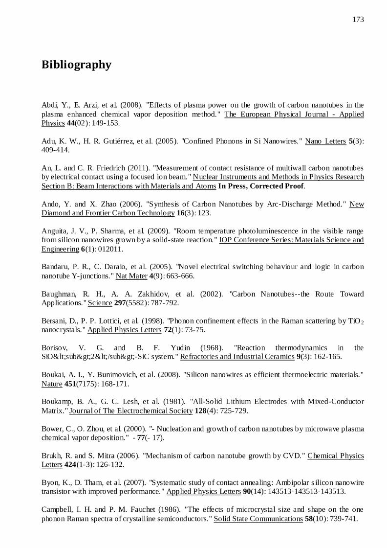
173
Bibliography
Abdi, Y., E. Arzi, et al. (2008). "Effects of plasma power on the growth of carbon nanotubes in the
plasma enhanced chemical vapor deposition method." The European Physical Journal - Applied Physics 44(02): 149-153.
Adu, K. W., H. R. Gutiérrez, et al. (2005). "Confined Phonons in Si Nanowires." Nano Letters 5(3): 409-414.
An, L. and C. R. Friedrich (2011). "Measurement of contact resistance of multiwall carbon nanotubes by electrical contact using a focused ion beam." Nuclear Instruments and Methods in Physics Research
Section B: Beam Interactions with Materials and Atoms In Press, Corrected Proof.
Ando, Y. and X. Zhao (2006). "Synthesis of Carbon Nanotubes by Arc-Discharge Method." New Diamond and Frontier Carbon Technology 16(3): 123.
Anguita, J. V., P. Sharma, et al. (2009). "Room temperature photoluminescence in the visible range from silicon nanowires grown by a solid-state reaction." IOP Conference Series: Materials Science and
Engineering 6(1): 012011. Bandaru, P. R., C. Daraio, et al. (2005). "Novel electrical switching behaviour and logic in carbon
nanotube Y-junctions." Nat Mater 4(9): 663-666.
Baughman, R. H., A. A. Zakhidov, et al. (2002). "Carbon Nanotubes--the Route Toward Applications." Science 297(5582): 787-792.
Bersani, D., P. P. Lottici, et al. (1998). "Phonon confinement effects in the Raman scattering by TiO 2 nanocrystals." Applied Physics Letters 72(1): 73-75.
Borisov, V. G. and B. F. Yudin (1968). "Reaction thermodynamics in the SiO<sub>2</sub>-SiC system." Refractories and Industrial Ceramics 9(3): 162-165.
Boukai, A. I., Y. Bunimovich, et al. (2008). "Silicon nanowires as efficient thermoelectric materials."
Nature 451(7175): 168-171. Boukamp, B. A., G. C. Lesh, et al. (1981). "All-Solid Lithium Electrodes with Mixed-Conductor
Matrix." Journal of The Electrochemical Society 128(4): 725-729.
Bower, C., O. Zhou, et al. (2000). "- Nucleation and growth of carbon nanotubes by microwave plasma chemical vapor deposition." - 77(- 17).
Brukh, R. and S. Mitra (2006). "Mechanism of carbon nanotube growth by CVD." Chemical Physics Letters 424(1-3): 126-132.
Byon, K., D. Tham, et al. (2007). "Systematic study of contact annealing: Ambipolar s ilicon nanowire transistor with improved performance." Applied Physics Letters 90(14): 143513-143513-143513.
Campbell, I. H. and P. M. Fauchet (1986). "The effects of microcrystal size and shape on the one
phonon Raman spectra of crystalline semiconductors." Solid State Communications 58(10): 739-741.
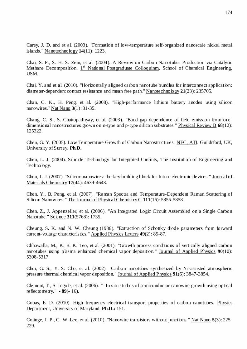
174
Carey, J. D. and et al. (2003). "Formation of low-temperature self-organized nanoscale nickel metal
islands." Nanotechnology 14(11): 1223.
Chai, S. P., S. H. S. Zein, et al. (2004). A Review on Carbon Nanotubes Production via Catalytic Methane Decomposition. 1st National Postgraduate Colloquinm. School of Chemical Engineering, USM.
Chai, Y. and et al. (2010). "Horizontally aligned carbon nanotube bundles for interconnect application:
diameter-dependent contact resistance and mean free path." Nanotechnology 21(23): 235705. Chan, C. K., H. Peng, et al. (2008). "High-performance lithium battery anodes using silicon
nanowires." Nat Nano 3(1): 31-35.
Chang, C. S., S. Chattopadhyay, et al. (2003). "Band-gap dependence of field emission from one-dimensional nanostructures grown on n-type and p-type silicon substrates." Physical Review B 68(12): 125322.
Chen, G. Y. (2005). Low Temperature Growth of Carbon Nanostructures. NEC, ATI. Guildrford, UK, University of Surrey. Ph.D.
Chen, L. J. (2004). Silicide Technology for Integrated Circuits, The Institution of Engineering and
Technology. Chen, L. J. (2007). "Silicon nanowires: the key building block for future electronic devices." Journal of
Materials Chemistry 17(44): 4639-4643.
Chen, Y., B. Peng, et al. (2007). "Raman Spectra and Temperature-Dependent Raman Scattering of Silicon Nanowires." The Journal of Physical Chemistry C 111(16): 5855-5858.
Chen, Z., J. Appenzeller, et al. (2006). "An Integrated Logic Circuit Assembled on a Single Carbon Nanotube." Science 311(5768): 1735.
Cheung, S. K. and N. W. Cheung (1986). "Extraction of Schottky diode parameters from forward current-voltage characteristics." Applied Physics Letters 49(2): 85-87.
Chhowalla, M., K. B. K. Teo, et al. (2001). "Growth process conditions of vertically aligned carbon
nanotubes using plasma enhanced chemical vapor deposition." Journal of Applied Physics 90(10): 5308-5317.
Choi, G. S., Y. S. Cho, et al. (2002). "Carbon nanotubes synthesized by Ni-assisted atmospheric pressure thermal chemical vapor deposition." Journal of Applied Physics 91(6): 3847-3854.
Clement, T., S. Ingole, et al. (2006). "- In situ studies of semiconductor nanowire growth using optical reflectometry." - 89(- 16).
Cobas, E. D. (2010). High frequency electrical transport properties of carbon nanotubes. Physics
Department, University of Maryland. Ph.D.: 151. Colinge, J.-P., C.-W. Lee, et al. (2010). "Nanowire transistors without junctions." Nat Nano 5(3): 225-
229.
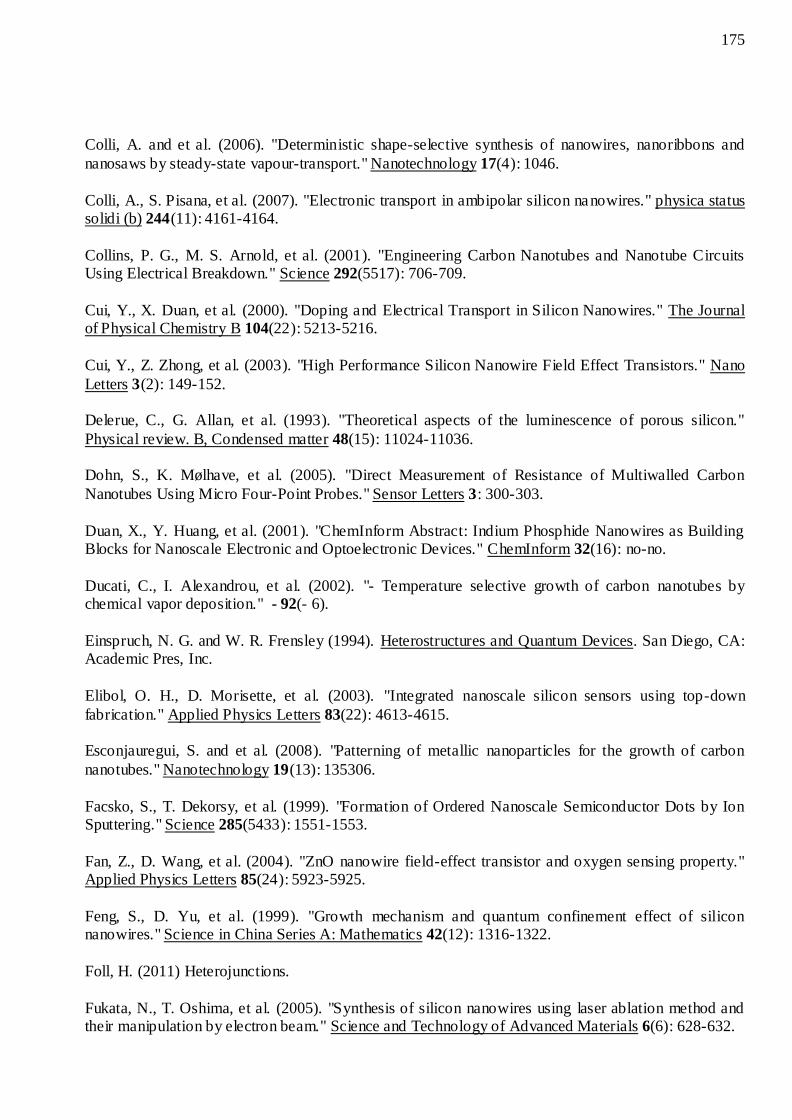
175
Colli, A. and et al. (2006). "Deterministic shape-selective synthesis of nanowires, nanoribbons and
nanosaws by steady-state vapour-transport." Nanotechnology 17(4): 1046.
Colli, A., S. Pisana, et al. (2007). "Electronic transport in ambipolar silicon nanowires." physica status solidi (b) 244(11): 4161-4164.
Collins, P. G., M. S. Arnold, et al. (2001). "Engineering Carbon Nanotubes and Nanotube Circuits Using Electrical Breakdown." Science 292(5517): 706-709.
Cui, Y., X. Duan, et al. (2000). "Doping and Electrical Transport in Silicon Nanowires." The Journal of Physical Chemistry B 104(22): 5213-5216.
Cui, Y., Z. Zhong, et al. (2003). "High Performance Silicon Nanowire Field Effect Transistors." Nano
Letters 3(2): 149-152. Delerue, C., G. Allan, et al. (1993). "Theoretical aspects of the luminescence of porous silicon."
Physical review. B, Condensed matter 48(15): 11024-11036. Dohn, S., K. Mølhave, et al. (2005). "Direct Measurement of Resistance of Multiwalled Carbon
Nanotubes Using Micro Four-Point Probes." Sensor Letters 3: 300-303.
Duan, X., Y. Huang, et al. (2001). "ChemInform Abstract: Indium Phosphide Nanowires as Building Blocks for Nanoscale Electronic and Optoelectronic Devices." ChemInform 32(16): no-no.
Ducati, C., I. Alexandrou, et al. (2002). "- Temperature selective growth of carbon nanotubes by chemical vapor deposition." - 92(- 6).
Einspruch, N. G. and W. R. Frensley (1994). Heterostructures and Quantum Devices. San Diego, CA: Academic Pres, Inc.
Elibol, O. H., D. Morisette, et al. (2003). "Integrated nanoscale silicon sensors using top-down
fabrication." Applied Physics Letters 83(22): 4613-4615. Esconjauregui, S. and et al. (2008). "Patterning of metallic nanoparticles for the growth of carbon
nanotubes." Nanotechnology 19(13): 135306.
Facsko, S., T. Dekorsy, et al. (1999). "Formation of Ordered Nanoscale Semiconductor Dots by Ion Sputtering." Science 285(5433): 1551-1553.
Fan, Z., D. Wang, et al. (2004). "ZnO nanowire field-effect transistor and oxygen sensing property." Applied Physics Letters 85(24): 5923-5925.
Feng, S., D. Yu, et al. (1999). "Growth mechanism and quantum confinement effect of silicon nanowires." Science in China Series A: Mathematics 42(12): 1316-1322.
Foll, H. (2011) Heterojunctions.
Fukata, N., T. Oshima, et al. (2005). "Synthesis of silicon nanowires using laser ablation method and their manipulation by electron beam." Science and Technology of Advanced Materials 6(6): 628-632.
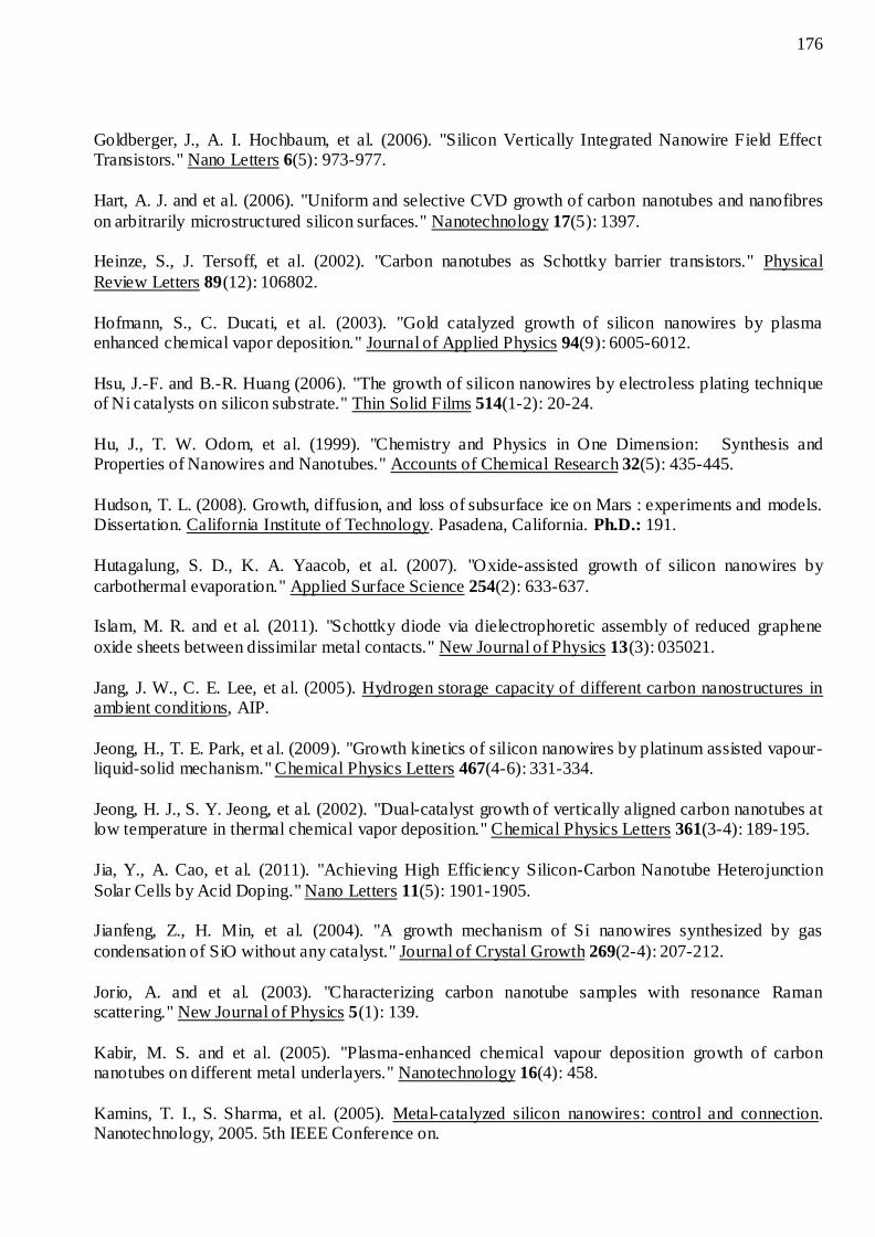
176
Goldberger, J., A. I. Hochbaum, et al. (2006). "Silicon Vertically Integrated Nanowire Field Effect Transistors." Nano Letters 6(5): 973-977.
Hart, A. J. and et al. (2006). "Uniform and selective CVD growth of carbon nanotubes and nanofibres
on arbitrarily microstructured silicon surfaces." Nanotechnology 17(5): 1397. Heinze, S., J. Tersoff, et al. (2002). "Carbon nanotubes as Schottky barrier transistors." Physical
Review Letters 89(12): 106802.
Hofmann, S., C. Ducati, et al. (2003). "Gold catalyzed growth of silicon nanowires by plasma enhanced chemical vapor deposition." Journal of Applied Physics 94(9): 6005-6012.
Hsu, J.-F. and B.-R. Huang (2006). "The growth of silicon nanowires by electroless plating technique of Ni catalysts on silicon substrate." Thin Solid Films 514(1-2): 20-24.
Hu, J., T. W. Odom, et al. (1999). "Chemistry and Physics in One Dimension: Synthesis and Properties of Nanowires and Nanotubes." Accounts of Chemical Research 32(5): 435-445.
Hudson, T. L. (2008). Growth, diffusion, and loss of subsurface ice on Mars : experiments and models. Dissertation. California Institute of Technology. Pasadena, California. Ph.D.: 191.
Hutagalung, S. D., K. A. Yaacob, et al. (2007). "Oxide-assisted growth of silicon nanowires by
carbothermal evaporation." Applied Surface Science 254(2): 633-637. Islam, M. R. and et al. (2011). "Schottky diode via dielectrophoretic assembly of reduced graphene
oxide sheets between dissimilar metal contacts." New Journal of Physics 13(3): 035021.
Jang, J. W., C. E. Lee, et al. (2005). Hydrogen storage capacity of different carbon nanostructures in ambient conditions, AIP.
Jeong, H., T. E. Park, et al. (2009). "Growth kinetics of silicon nanowires by platinum assisted vapour-liquid-solid mechanism." Chemical Physics Letters 467(4-6): 331-334.
Jeong, H. J., S. Y. Jeong, et al. (2002). "Dual-catalyst growth of vertically aligned carbon nanotubes at low temperature in thermal chemical vapor deposition." Chemical Physics Letters 361(3-4): 189-195.
Jia, Y., A. Cao, et al. (2011). "Achieving High Efficiency Silicon-Carbon Nanotube Heterojunction
Solar Cells by Acid Doping." Nano Letters 11(5): 1901-1905. Jianfeng, Z., H. Min, et al. (2004). "A growth mechanism of Si nanowires synthesized by gas
condensation of SiO without any catalyst." Journal of Crystal Growth 269(2-4): 207-212.
Jorio, A. and et al. (2003). "Characterizing carbon nanotube samples with resonance Raman scattering." New Journal of Physics 5(1): 139.
Kabir, M. S. and et al. (2005). "Plasma-enhanced chemical vapour deposition growth of carbon nanotubes on different metal underlayers." Nanotechnology 16(4): 458.
Kamins, T. I., S. Sharma, et al. (2005). Metal-catalyzed silicon nanowires: control and connection. Nanotechnology, 2005. 5th IEEE Conference on.
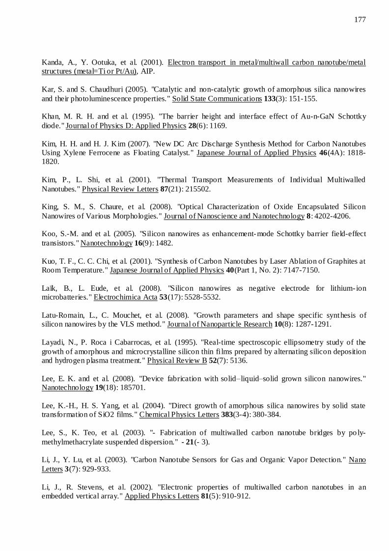
177
Kanda, A., Y. Ootuka, et al. (2001). Electron transport in metal/multiwall carbon nanotube/metal structures (metal=Ti or Pt/Au), AIP.
Kar, S. and S. Chaudhuri (2005). "Catalytic and non-catalytic growth of amorphous silica nanowires
and their photoluminescence properties." Solid State Communications 133(3): 151-155. Khan, M. R. H. and et al. (1995). "The barrier height and interface effect of Au-n-GaN Schottky
diode." Journal of Physics D: Applied Physics 28(6): 1169.
Kim, H. H. and H. J. Kim (2007). "New DC Arc Discharge Synthesis Method for Carbon Nanotubes Using Xylene Ferrocene as Floating Catalyst." Japanese Journal of Applied Physics 46(4A): 1818-1820.
Kim, P., L. Shi, et al. (2001). "Thermal Transport Measurements of Individual Multiwalled
Nanotubes." Physical Review Letters 87(21): 215502. King, S. M., S. Chaure, et al. (2008). "Optical Characterization of Oxide Encapsulated Silicon
Nanowires of Various Morphologies." Journal of Nanoscience and Nanotechnology 8: 4202-4206. Koo, S.-M. and et al. (2005). "Silicon nanowires as enhancement-mode Schottky barrier field-effect
transistors." Nanotechnology 16(9): 1482.
Kuo, T. F., C. C. Chi, et al. (2001). "Synthesis of Carbon Nanotubes by Laser Ablation of Graphites at Room Temperature." Japanese Journal of Applied Physics 40(Part 1, No. 2): 7147-7150.
Laïk, B., L. Eude, et al. (2008). "Silicon nanowires as negative electrode for lithium-ion microbatteries." Electrochimica Acta 53(17): 5528-5532.
Latu-Romain, L., C. Mouchet, et al. (2008). "Growth parameters and shape specific synthesis of silicon nanowires by the VLS method." Journal of Nanoparticle Research 10(8): 1287-1291.
Layadi, N., P. Roca i Cabarrocas, et al. (1995). "Real-time spectroscopic ellipsometry study of the
growth of amorphous and microcrystalline silicon thin films prepared by alternating silicon deposition and hydrogen plasma treatment." Physical Review B 52(7): 5136.
Lee, E. K. and et al. (2008). "Device fabrication with solid–liquid–solid grown silicon nanowires." Nanotechnology 19(18): 185701.
Lee, K.-H., H. S. Yang, et al. (2004). "Direct growth of amorphous silica nanowires by solid state transformation of SiO2 films." Chemical Physics Letters 383(3-4): 380-384.
Lee, S., K. Teo, et al. (2003). "- Fabrication of multiwalled carbon nanotube bridges by po ly-
methylmethacrylate suspended dispersion." - 21(- 3). Li, J., Y. Lu, et al. (2003). "Carbon Nanotube Sensors for Gas and Organic Vapor Detection." Nano
Letters 3(7): 929-933.
Li, J., R. Stevens, et al. (2002). "Electronic properties of multiwalled carbon nanotubes in an embedded vertical array." Applied Physics Letters 81(5): 910-912.
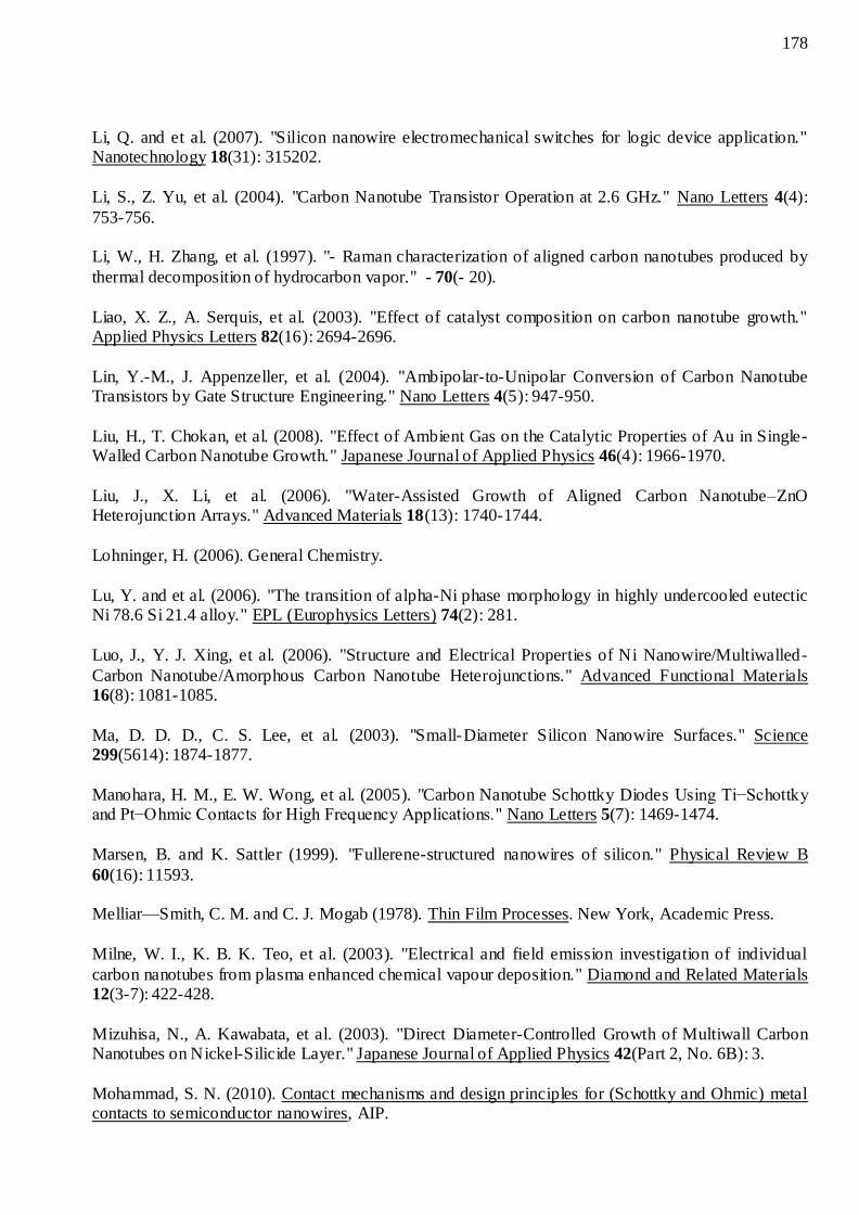
178
Li, Q. and et al. (2007). "Silicon nanowire electromechanical switches for logic device application." Nanotechnology 18(31): 315202.
Li, S., Z. Yu, et al. (2004). "Carbon Nanotube Transistor Operation at 2.6 GHz." Nano Letters 4(4):
753-756. Li, W., H. Zhang, et al. (1997). "- Raman characterization of aligned carbon nanotubes produced by
thermal decomposition of hydrocarbon vapor." - 70(- 20).
Liao, X. Z., A. Serquis, et al. (2003). "Effect of catalyst composition on carbon nanotube growth." Applied Physics Letters 82(16): 2694-2696.
Lin, Y.-M., J. Appenzeller, et al. (2004). "Ambipolar-to-Unipolar Conversion of Carbon Nanotube Transistors by Gate Structure Engineering." Nano Letters 4(5): 947-950.
Liu, H., T. Chokan, et al. (2008). "Effect of Ambient Gas on the Catalytic Properties of Au in Single-Walled Carbon Nanotube Growth." Japanese Journal of Applied Physics 46(4): 1966-1970.
Liu, J., X. Li, et al. (2006). "Water-Assisted Growth of Aligned Carbon Nanotube–ZnO Heterojunction Arrays." Advanced Materials 18(13): 1740-1744.
Lohninger, H. (2006). General Chemistry.
Lu, Y. and et al. (2006). "The transition of alpha-Ni phase morphology in highly undercooled eutectic Ni 78.6 Si 21.4 alloy." EPL (Europhysics Letters) 74(2): 281.
Luo, J., Y. J. Xing, et al. (2006). "Structure and Electrical Properties of Ni Nanowire/Multiwalled-
Carbon Nanotube/Amorphous Carbon Nanotube Heterojunctions." Advanced Functional Materials 16(8): 1081-1085.
Ma, D. D. D., C. S. Lee, et al. (2003). "Small-Diameter Silicon Nanowire Surfaces." Science 299(5614): 1874-1877.
Manohara, H. M., E. W. Wong, et al. (2005). "Carbon Nanotube Schottky Diodes Using Ti−Schottky and Pt−Ohmic Contacts for High Frequency Applications." Nano Letters 5(7): 1469-1474.
Marsen, B. and K. Sattler (1999). "Fullerene-structured nanowires of silicon." Physical Review B
60(16): 11593. Melliar—Smith, C. M. and C. J. Mogab (1978). Thin Film Processes. New York, Academic Press.
Milne, W. I., K. B. K. Teo, et al. (2003). "Electrical and field emission investigation of individual
carbon nanotubes from plasma enhanced chemical vapour deposition." Diamond and Related Materials 12(3-7): 422-428.
Mizuhisa, N., A. Kawabata, et al. (2003). "Direct Diameter-Controlled Growth of Multiwall Carbon Nanotubes on Nickel-Silicide Layer." Japanese Journal of Applied Physics 42(Part 2, No. 6B): 3.
Mohammad, S. N. (2010). Contact mechanisms and design principles for (Schottky and Ohmic) metal contacts to semiconductor nanowires, AIP.
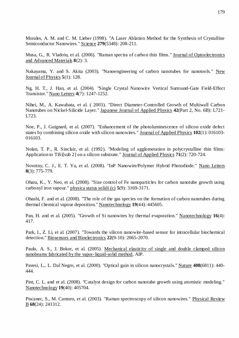
179
Morales, A. M. and C. M. Lieber (1998). "A Laser Ablation Method for the Synthesis of Crystalline Semiconductor Nanowires." Science 279(5348): 208-211.
Musa, G., R. Vladoiu, et al. (2006). "Raman spectra of carbon thin films." Journal of Optoelectronics
and Advanced Materials 8(2): 3. Nakayama, Y. and S. Akita (2003). "Nanoengineering of carbon nanotubes for nanotools." New
Journal of Physics 5(1): 128.
Ng, H. T., J. Han, et al. (2004). "Single Crystal Nanowire Vertical Surround-Gate Field-Effect Transistor." Nano Letters 4(7): 1247-1252.
Nihei, M., A. Kawabata, et al. ( 2003). "Direct Diameter-Controlled Growth of Multiwall Carbon Nanotubes on Nickel-Silicide Layer." Japanese Journal of Applied Physics 42(Part 2, No. 6B): L721-
L723. Noe, P., J. Guignard, et al. (2007). "Enhancement of the photoluminescence of silicon oxide defect
states by combining silicon oxide with silicon nanowires." Journal of Applied Physics 102(1): 016103-016103.
Nolan, T. P., R. Sinclair, et al. (1992). "Modeling of agglomeration in polycrystalline thin films: Application to TiSi[sub 2] on a silicon substrate." Journal of Applied Physics 71(2): 720-724.
Novotny, C. J., E. T. Yu, et al. (2008). "InP Nanowire/Polymer Hybrid Photodiode." Nano Letters 8(3): 775-779.
Ohara, K., Y. Neo, et al. (2008). "Size control of Fe nanoparticles for carbon nanotube growth using
carbonyl iron vapour." physica status solidi (c) 5(9): 3169-3171. Ohashi, F. and et al. (2008). "The role of the gas species on the formation of carbon nanotubes during
thermal chemical vapour deposition." Nanotechnology 19(44): 445605.
Pan, H. and et al. (2005). "Growth of Si nanowires by thermal evaporation." Nanotechnology 16(4): 417.
Park, I., Z. Li, et al. (2007). "Towards the silicon nanowire-based sensor for intracellular biochemical detection." Biosensors and Bioelectronics 22(9-10): 2065-2070.
Paulo, A. S., J. Bokor, et al. (2005). Mechanical elasticity of single and double clamped silicon nanobeams fabricated by the vapor- liquid-solid method, AIP.
Pavesi, L., L. Dal Negro, et al. (2000). "Optical gain in silicon nanocrystals." Nature 408(6811): 440-
444. Pint, C. L. and et al. (2008). "Catalyst design for carbon nanotube growth using atomistic modeling."
Nanotechnology 19(40): 405704.
Piscanec, S., M. Cantoro, et al. (2003). "Raman spectroscopy of silicon nanowires." Physical Review B 68(24): 241312.
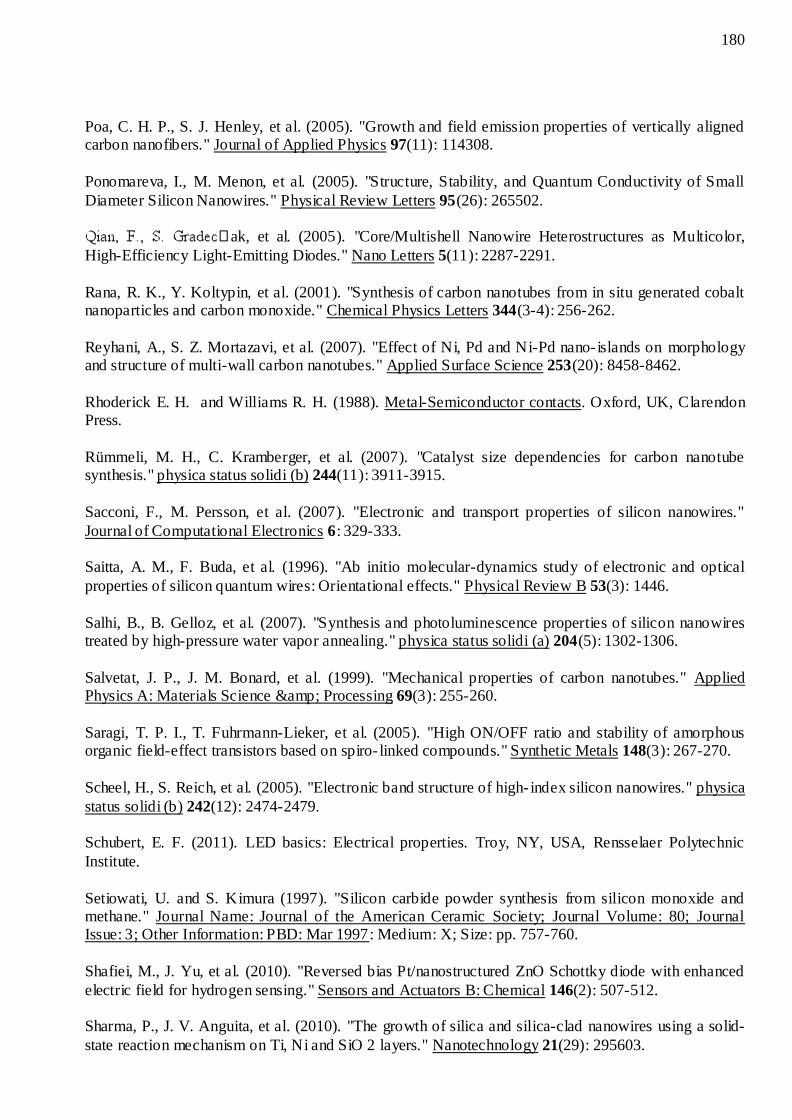
180
Poa, C. H. P., S. J. Henley, et al. (2005). "Growth and field emission properties of vertically aligned carbon nanofibers." Journal of Applied Physics 97(11): 114308.
Ponomareva, I., M. Menon, et al. (2005). "Structure, Stability, and Quantum Conductivity of Small
Diameter Silicon Nanowires." Physical Review Letters 95(26): 265502.
ak, et al. (2005). "Core/Multishell Nanowire Heterostructures as Multicolor,
High-Efficiency Light-Emitting Diodes." Nano Letters 5(11): 2287-2291.
Rana, R. K., Y. Koltypin, et al. (2001). "Synthesis of carbon nanotubes from in situ generated cobalt nanoparticles and carbon monoxide." Chemical Physics Letters 344(3-4): 256-262.
Reyhani, A., S. Z. Mortazavi, et al. (2007). "Effect of Ni, Pd and Ni-Pd nano- islands on morphology and structure of multi-wall carbon nanotubes." Applied Surface Science 253(20): 8458-8462.
Rhoderick E. H. and Williams R. H. (1988). Metal-Semiconductor contacts. Oxford, UK, Clarendon Press.
Rümmeli, M. H., C. Kramberger, et al. (2007). "Catalyst size dependencies for carbon nanotube synthesis." physica status solidi (b) 244(11): 3911-3915.
Sacconi, F., M. Persson, et al. (2007). "Electronic and transport properties of silicon nanowires."
Journal of Computational Electronics 6: 329-333. Saitta, A. M., F. Buda, et al. (1996). "Ab initio molecular-dynamics study of electronic and optical
properties of silicon quantum wires: Orientational effects." Physical Review B 53(3): 1446.
Salhi, B., B. Gelloz, et al. (2007). "Synthesis and photoluminescence properties of silicon nanowires treated by high-pressure water vapor annealing." physica status solidi (a) 204(5): 1302-1306.
Salvetat, J. P., J. M. Bonard, et al. (1999). "Mechanical properties of carbon nanotubes." Applied Physics A: Materials Science & Processing 69(3): 255-260.
Saragi, T. P. I., T. Fuhrmann-Lieker, et al. (2005). "High ON/OFF ratio and stability of amorphous organic field-effect transistors based on spiro- linked compounds." Synthetic Metals 148(3): 267-270.
Scheel, H., S. Reich, et al. (2005). "Electronic band structure of high- index silicon nanowires." physica
status solidi (b) 242(12): 2474-2479. Schubert, E. F. (2011). LED basics: Electrical properties. Troy, NY, USA, Rensselaer Polytechnic
Institute.
Setiowati, U. and S. Kimura (1997). "Silicon carbide powder synthesis from silicon monoxide and methane." Journal Name: Journal of the American Ceramic Society; Journal Volume: 80; Journal Issue: 3; Other Information: PBD: Mar 1997: Medium: X; Size: pp. 757-760.
Shafiei, M., J. Yu, et al. (2010). "Reversed bias Pt/nanostructured ZnO Schottky diode with enhanced
electric field for hydrogen sensing." Sensors and Actuators B: Chemical 146(2): 507-512. Sharma, P., J. V. Anguita, et al. (2010). "The growth of silica and silica-clad nanowires using a solid-
state reaction mechanism on Ti, Ni and SiO 2 layers." Nanotechnology 21(29): 295603.
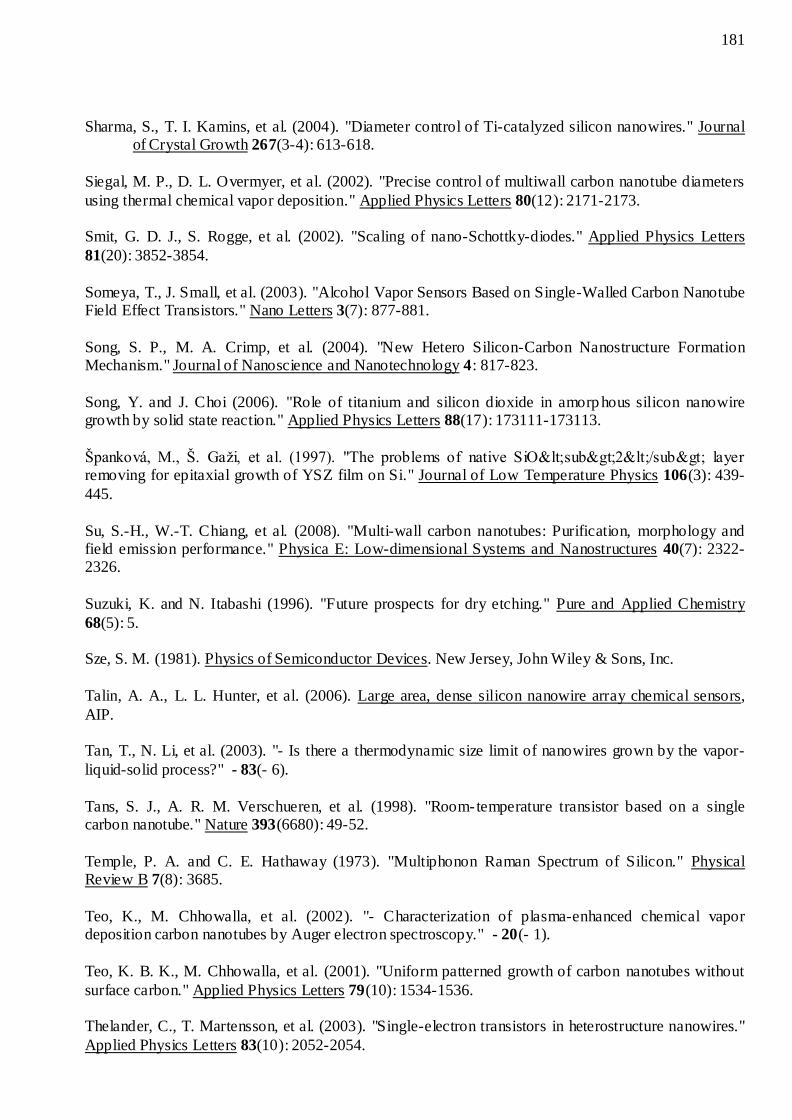
181
Sharma, S., T. I. Kamins, et al. (2004). "Diameter control of Ti-catalyzed silicon nanowires." Journal of Crystal Growth 267(3-4): 613-618.
Siegal, M. P., D. L. Overmyer, et al. (2002). "Precise control of multiwall carbon nanotube diameters
using thermal chemical vapor deposition." Applied Physics Letters 80(12): 2171-2173. Smit, G. D. J., S. Rogge, et al. (2002). "Scaling of nano-Schottky-diodes." Applied Physics Letters
81(20): 3852-3854.
Someya, T., J. Small, et al. (2003). "Alcohol Vapor Sensors Based on Single-Walled Carbon Nanotube Field Effect Transistors." Nano Letters 3(7): 877-881.
Song, S. P., M. A. Crimp, et al. (2004). "New Hetero Silicon-Carbon Nanostructure Formation Mechanism." Journal of Nanoscience and Nanotechnology 4: 817-823.
Song, Y. and J. Choi (2006). "Role of titanium and silicon dioxide in amorp hous silicon nanowire growth by solid state reaction." Applied Physics Letters 88(17): 173111-173113.
Španková, M., Š. Gaži, et al. (1997). "The problems of native SiO<sub>2</sub> layer removing for epitaxial growth of YSZ film on Si." Journal of Low Temperature Physics 106(3): 439-
445.
Su, S.-H., W.-T. Chiang, et al. (2008). "Multi-wall carbon nanotubes: Purification, morphology and field emission performance." Physica E: Low-dimensional Systems and Nanostructures 40(7): 2322-2326.
Suzuki, K. and N. Itabashi (1996). "Future prospects for dry etching." Pure and Applied Chemistry
68(5): 5. Sze, S. M. (1981). Physics of Semiconductor Devices. New Jersey, John Wiley & Sons, Inc.
Talin, A. A., L. L. Hunter, et al. (2006). Large area, dense silicon nanowire array chemical sensors,
AIP. Tan, T., N. Li, et al. (2003). "- Is there a thermodynamic size limit of nanowires grown by the vapor-
liquid-solid process?" - 83(- 6).
Tans, S. J., A. R. M. Verschueren, et al. (1998). "Room-temperature transistor based on a single carbon nanotube." Nature 393(6680): 49-52.
Temple, P. A. and C. E. Hathaway (1973). "Multiphonon Raman Spectrum of Silicon." Physical Review B 7(8): 3685.
Teo, K., M. Chhowalla, et al. (2002). "- Characterization of plasma-enhanced chemical vapor deposition carbon nanotubes by Auger electron spectroscopy." - 20(- 1).
Teo, K. B. K., M. Chhowalla, et al. (2001). "Uniform patterned growth of carbon nanotubes without
surface carbon." Applied Physics Letters 79(10): 1534-1536. Thelander, C., T. Martensson, et al. (2003). "Single-electron transistors in heterostructure nanowires."
Applied Physics Letters 83(10): 2052-2054.
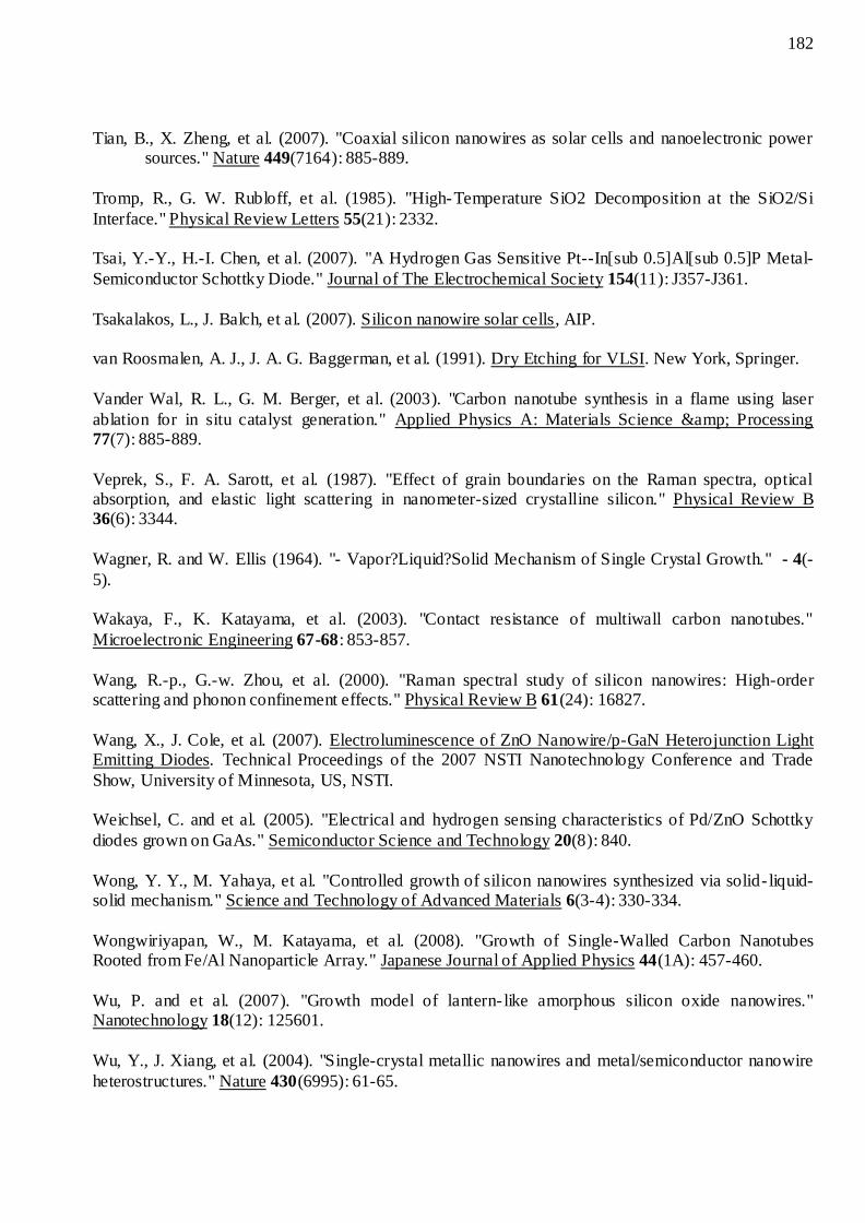
182
Tian, B., X. Zheng, et al. (2007). "Coaxial silicon nanowires as solar cells and nanoelectronic power sources." Nature 449(7164): 885-889.
Tromp, R., G. W. Rubloff, et al. (1985). "High-Temperature SiO2 Decomposition at the SiO2/Si
Interface." Physical Review Letters 55(21): 2332. Tsai, Y.-Y., H.-I. Chen, et al. (2007). "A Hydrogen Gas Sensitive Pt--In[sub 0.5]Al[sub 0.5]P Metal-
Semiconductor Schottky Diode." Journal of The Electrochemical Society 154(11): J357-J361.
Tsakalakos, L., J. Balch, et al. (2007). Silicon nanowire solar cells, AIP. van Roosmalen, A. J., J. A. G. Baggerman, et al. (1991). Dry Etching for VLSI. New York, Springer.
Vander Wal, R. L., G. M. Berger, et al. (2003). "Carbon nanotube synthesis in a flame using laser
ablation for in situ catalyst generation." Applied Physics A: Materials Science & Processing 77(7): 885-889.
Veprek, S., F. A. Sarott, et al. (1987). "Effect of grain boundaries on the Raman spectra, optical absorption, and elastic light scattering in nanometer-sized crystalline silicon." Physical Review B 36(6): 3344.
Wagner, R. and W. Ellis (1964). "- Vapor?Liquid?Solid Mechanism of Single Crystal Growth." - 4(-
5). Wakaya, F., K. Katayama, et al. (2003). "Contact resistance of multiwall carbon nanotubes."
Microelectronic Engineering 67-68: 853-857.
Wang, R.-p., G.-w. Zhou, et al. (2000). "Raman spectral study of silicon nanowires: High-order scattering and phonon confinement effects." Physical Review B 61(24): 16827.
Wang, X., J. Cole, et al. (2007). Electroluminescence of ZnO Nanowire/p-GaN Heterojunction Light Emitting Diodes. Technical Proceedings of the 2007 NSTI Nanotechnology Conference and Trade
Show, University of Minnesota, US, NSTI. Weichsel, C. and et al. (2005). "Electrical and hydrogen sensing characteristics of Pd/ZnO Schottky
diodes grown on GaAs." Semiconductor Science and Technology 20(8): 840.
Wong, Y. Y., M. Yahaya, et al. "Controlled growth of silicon nanowires synthesized via solid- liquid-solid mechanism." Science and Technology of Advanced Materials 6(3-4): 330-334.
Wongwiriyapan, W., M. Katayama, et al. (2008). "Growth of Single-Walled Carbon Nanotubes Rooted from Fe/Al Nanoparticle Array." Japanese Journal of Applied Physics 44(1A): 457-460.
Wu, P. and et al. (2007). "Growth model of lantern- like amorphous silicon oxide nanowires." Nanotechnology 18(12): 125601.
Wu, Y., J. Xiang, et al. (2004). "Single-crystal metallic nanowires and metal/semiconductor nanowire
heterostructures." Nature 430(6995): 61-65.
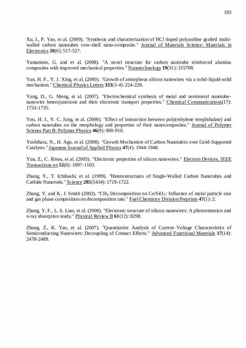
183
Xu, J., P. Yao, et al. (2009). "Synthesis and characterization of HCl doped polyaniline grafted multi-walled carbon nanotubes core-shell nano-composite." Journal of Materials Science: Materials in
Electronics 20(6): 517-527.
Yamamoto, G. and et al. (2008). "A novel structure for carbon nanotube reinforced alumina composites with improved mechanical properties." Nanotechnology 19(31): 315708.
Yan, H. F., Y. J. Xing, et al. (2000). "Growth of amorphous silicon nanowires via a solid-liquid-solid mechanism." Chemical Physics Letters 323(3-4): 224-228.
Yang, D., G. Meng, et al. (2007). "Electrochemical synthesis of metal and semimetal nanotube-nanowire heterojunctions and their electronic transport properties." Chemical Communications(17):
1733-1735.
Yoo, H. J., Y. C. Jung, et al. (2008). "Effect of interaction between poly(ethylene terephthalate) and carbon nanotubes on the morphology and properties of their nanocomposites." Journal of Polymer Science Part B: Polymer Physics 46(9): 900-910.
Yoshihara, N., H. Ago, et al. (2008). "Growth Mechanism of Carbon Nanotubes over Gold-Supported Catalysts." Japanese Journal of Applied Physics 47(4): 1944-1948.
Yun, Z., C. Rivas, et al. (2005). "Electronic properties of silicon nanowires." Electron Devices, IEEE
Transactions on 52(6): 1097-1103. Zhang, Y., T. Ichihashi, et al. (1999). "Heterostructures of Single-Walled Carbon Nanotubes and
Carbide Nanorods." Science 285(5434): 1719-1722.
Zhang, Y. and K. J. Smith (2002). "CH4 Decomposition on Co/SiO2 : Influence of metal particle size and gas phase composition on decomposition rate." Fuel Chemistry Division Preprints 47(1): 2.
Zhang, Y. F., L. S. Liao, et al. (2000). "Electronic structure of silicon nanowires: A photoemission and x-ray absorption study." Physical Review B 61(12): 8298.
Zhang, Z., K. Yao, et al. (2007). "Quantitative Analysis of Current–Voltage Characteristics of Semiconducting Nanowires: Decoupling of Contact Effects." Advanced Functional Materials 17(14):
2478-2489.