Embed Size (px)
Citation preview

H740D power supply maintenance manual


c
l
H740D power supply maintenance manual
DEC-II-H740A-A-D
. digital equipment corporation • maynard, massachusetts .
Copyright © 1973 by Digital Equipment Corporation
The material in this manual is for informational purposes and is subject to change without notice.
Digital Equipment Corporation assumes no responsibility for any errors which may appear in this manuaL
The following are trademarks of Digital Equipment Corporation, Ma¥nard, Massachusetts:
DEC FLIP CHIP DIGITAL UNIBUS
PDP FOCAL COMPUTER LAB
1st Edition, June 1973
c
(-

(
CHAPTER 1
1.1 1.2 1.3 1.3.1 1.3.2 1.3.3 1.3.4 1.3.5 1.3.6 1.3.7 1.4
CHAPTER 2
2.1 2.2 2.2.1 2.2.2 2.2.3 2.2.4 2.3 2.3.1 2.3.2 2.3.3 2.3.4 2.3.5
CHAPTER 3
3.1 3.2 3.3 3.4 3.5 3.6 3.6.1 3.6.2 3.6.3 3.6.4 3.6.5 3.6.6 3.6.7
CONTENTS
Page
GENERAL INFORMATION
INTRODUCTION ....................... . . . . . . . . . . . . . .. 1-1 GENERAL DESCRIPTION ................. . PHYSICAL DESCRIPTION .................. .
Power Supply Chassis ................................ . tine Set ....................................... . Transformer Assembly ........... . DC Regulator Module ........... .
1-1 1-1 1-3 1-3 1-4 1-4
Cooling Fan ................ . . . . . . . . . . . . . . .. 1-6 AC Harness ................. . DCHarness .....
H740D SPECIFICATIONS
INSTALLATION
1-6 1-7 1-7
INTRODUCTION ...................................... 2-1 POWER SUPPLY CONFIGURATION ............................ 2-1
Space Requirements .................................. 2-1 Environmental Requirements ............................. 2-1 Power Requirements .................................. 2-1 Cable Requirements .................................. 2-1
INSTALLATION PROCEDURES .............................. 2-1 Inspection ....................................... 2-2 Mounting the H740D ................................. 2-2 AC Power Connection ................................. 2-2 Initial Power Turn-On ............... . . . . . . . . . . . . .. 2-3 Connecting the H740D to the Device ......................... 2-3
PRINCIPLES OF OPERATION
INTRODUCTION ...................................... 3-1 LINE SET .......................................... 3-1 THERMOSTAT ....................................... 3-2 CQOLINGFAN ....................................... 3-2 TRANSFORMER ....................................... 3-2 DC REGULATOR MODULE ................................ 3-2
Generation of Raw DCVoltages ........................... . 3-4 LTC L Circuit ..................................... 3-4 AC LO L and DC LO L Circuits ............................ 3-6 PWR OK L Circuit ....;.............................. + 15 V Regulator Circuit +5 V Regulator Circuit . -15 V Regulator Circuit
iii
3-7 3-7 3-8 3-9
CHAPTER 4
4.1 4.2 4.3 4.4 4.4.1 4.4.2 4.4.3
Figure No.
1-1 1-2 1-3 1-4 1-5 1-6 2-1 3-1 3-2 3-3 3-4 3-5 3-6 3-7 3-8 3-9 3-10 3-11 4-1 4-2
Table No.
1-1 1-2 1-3 4-1
MAINTENANCE
INTRODUCTION ADJUSTMENTS .... CIRCUIT WAVEFORMS TROUBLESHOOTING
Troubleshooting Rules Troubleshooting Hints Troubleshooting Chart
, ,
CONTENTS (Cont)
· . . .~ . . . .' . . . . .'.
· ~ . . . . . . .. . . . ~ . .0' •• e' •• ' ••••
· ............ " ... .
ILLUSTRATIONS
Title
Page
. . . . .. 4-1 4-1 4-1 4-4 4-4 4-4 4-4
Page
H740D Power Supply Components ........................ 1-2 Line Set ....... . Transformer Assembly . ...... . . . . . . . . . . . . de Regulator Module . . . .. ....•. .... . . . . . . . . . ac Harness ....... . ............ , .. , .. , " ............. . de Harness ....... . .....................•.......... H740D Connectors . . . . . . . . . . . . . ; . . , • . . . . . . . . . . . . . . . . . . . . Power Supply Block Diagram ............••..•.... ..... . H740D Power Supply, Wiring Diagram ......... ; . ; ........... . 115 V Connection, Simplified Schematic Diagram ...•. . . . . . . . . . 230 V Connection, Simplified Schematic Diagram . , . ... . . . . . . . . . . . de Regulator Module, Block Diagram ..........,............ Rectifier and LTC L Circuits ..................•. ~ ........... . AC LO L and DC LO L Circuits ........... ...•.......
1-3 1-4 1-5 1-6 1-7 2-2 3-1 3-3 3-4 3-4 3-5 3-6 3-6
PWR OK L Circuit ... .................. . · . . . . . .. 3-7 + 15 V Regulator Circuit .......................... . +5 V Regulator Circuit ........•..•................ -15 V Regulator Circuit ........... . ............ . +5 V Regulator Circuit Waveforms ...... . . . . . -15 V Regulator Circuit Waveforms ..... . ............ .
TABLES
Title
Power Supply Input SpeCifications . .. . . . . . . . . . Power Supply Output Specifications .........•..... Mechanical and Environmental SpeCifications ... . Troubleshooting Chart ..................... .
iv
· . . . . . .. 3-8 · ... " . .. 3-8
. 3-10 4-2
. 4-3
Page
1-8 1-9
1-13 4-5
C
H740D POWER SUPPLY MAINTENANCE MANUAL
f'

L./

CHAPTER 1 GENERAL INFORMATION
1.1 INTRODUCTION
This manual provides a complete description of the H740D Power Supply. Included are functional and circuit level descriptions, physical descriptions of the power supply and components, power supply specifications, installation information, and maintenance procedures.
1.2 GENERAL DESCRIPTION
The H740D Power Supply is a forced air-cooled unit that converts single-phase 115 Vor 230 V nominal, 47-63 Hz line voltage to three regulated output voltages. The output voltages and their principal uses and characteristics are:
Voltage
+15 V +5V -15 V
Use
Communication circuits IC logic Core memory
Characteristics
Series regulated and overcurrent protected Switching regulated and overvoltage and overcurrent protected Switching regulated and overvoltage and overcurrent protected
In addition, the H740D generates the following control signals: power fail early warning signals (AC LO L and DC LO L), an alternate AC LO L signal (PWR OK L), and a clock signal (LTC L).
The power supply is completely contained in theH740D chassis with one 3-wire input power cord (With plug) and one IS-socket Mate-N-Lok output connector, both accessible from the rear of the chassis.
The unit is equipped with overload and overtemperature protection devices. An input power circuit breaker removes power if input current is excessive (7 A @ 1I5V, 4 A @ 230 V). A thermostat, mounted on the power supply heat sink, shuts down the power supply whenever heat sink temperature becomes excessive (1000 C).
1.3 PHYSICAL DESCRIPTION
The power supply (Figure 1-1) consists of five subassemblies and two cable harnesses: power supply chassis, line set, transformer, dc regulator module, 3-inch fan, ac harness, and dc harness. Refer to engineering drawing D-UA-H740-D-0 for a cutaway view of the H740D.
NOTE Although the line set is actually not part of the H740D Power Supply, a line set accompanies each H740D delivered and is mounted in the H740D chassis. Hence, for the convenience of the customer and Digital, the line set is treated as an integral part of the H740D Power Supply in this manual.
1-1

AIR FLOW
N
/----"\
POWE R SUPPLY CHASSIS (5309975)
COOLING. FAN ( 1210719)
LINE SET (BC05H or BC05J)
Figure 1-1 H740D Power Supply Components
(\
('
AC HARNESS (7008810)
DC REG.ULATOR MODULE (5409728)
, ~
DC HARNESS (7008811)
TRANSFORMER (700872a)
~

(
. .
(
1.3.1 Power Supply Chassis
The 5309975 chassis is a 3-1/2 in. high by 19 in. wide by 8 in. deep metal box that houses the power supply components. The box can be mounted in the rack or on the door using four bolts.
1.3.2 Line Set
The line set (Figure 1·2) adapts the power supply to the ac power source. Two different models are used: BC05H for 115 V operation and BC05J for 230 V operation. The line set is mounted in the rear of the power supply chassis by two 6-32 X 1/4 in. Phillips pan head screws. The unit consists of the H400 Power Control, a 6·ft line cord, and a 3-prong connector. The power control (engineering drawing D·UA·H400-Q-0) consists of a sing1e~pole thermal circuit breaker (7 A for 115 V operation, 4 A for 230 V operation), two RFI capacitors,. and a 6·socket Mate·N-Lok connector that is jumpered for 115 V or 230 V operation. The power control components are mounted on a sheet metal bracket with a slide-on cover that is locked in place by a 6-32 X 1/4 in. Phillips pan head screw. The line cord, with a strain relief grommet, is installed through the sheet metal bracket; Two different types of ac plugs are attached to the line cord. The BC05H line set uses NEMA plug no. 5·15P. The BC05J line set uses NEMA plug no. 6·15P. (Refer to Figure 2·1 for complete plug specifications~) .
Figure 1-2 Line Set
1·3
With the power supply completely assembled, the line cord and the circuit breaker reset button are accessible from (-the rear of the. power supply chassis. Note that the number on the reset button indicates the trip current of the '. circuit breaker.
NOTE When ordering the H740D Power Supply, the line set must be ordered separately. Line set model BC05H is used for 115 V operation and model BC05J is used for 230 V operation.
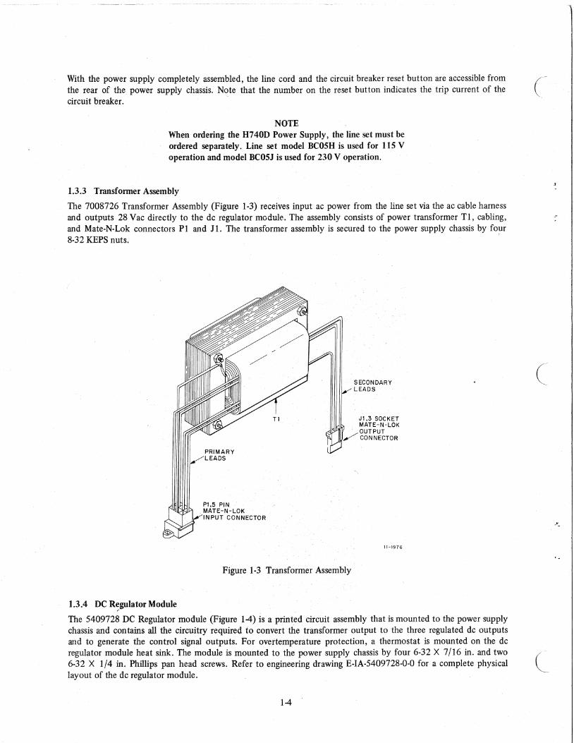
1.3.3 Transformer Assembly
The 7008726 Transformer Assembly (Figure 1-3) receives input ac power from the line set via the ac cable harness and outputs 28 Vac directly to the dc regulator module. The assembly consists of power transformer Tl, cabling, and Mate-N-Lok connectors PI and J1. The transformer assembly is secured to the power supply chassis by four 8-32 KEPS nuts. '
Figure 1-3 Transformer Assembly
1.3.4 DC R~gulator Module
SECONDARY LEADS
Jl,3 SOCKET MATE-N-LOK OUTPUT
NECTOR
11-1976
The 5409728 DC Regulator module (Figure 1-4) is a printed circuit assembly that is mounted to the power supply chassis and contains all the circuitry required to convert the transformer output to the three regulated dc outputs and to generate the control signal outputs. For overtemperature protection, a thermostat is mounted on the dc
c
regulator module heat sink. The module is mounted to the power supply chassis by four 6-32 X 7/16 in. and two ( 6-32 X 1/4 in. Phillips pan head screws. Refer to engineering drawing E-IA-S409728-0-0 for a complete physical ~ layout of the dc regulator module. -
1-4
· -

(
( '-
C14
DC OUTPUT MATE-N-LOK CONNECTOR
+15V ADJUSTMENT POTENTIOMETER
THERMOSTAT MATE-N-LOK CONNECTOR
Ll
Top View
ADJUSTMENT POTENTIOMETER
-15V ADJUSTMENT POTENTIOMETER
THERMOSTAT
Bottom View
Figure 1-4 de Regulator Module
1-5
HEAT SINK
ACINPUT MATE-N-LOK CONNECTOR
PICO FUSES

The dc regulator module consists of many small components assembled into a compact package. The printed circuit board is approximately 5 in. X 10 in. with all points on the circuit accessible from the top. The heat sink is mounted on top of the printed c:rcuit board. The power transistors and power rectifiers are bolted to shelves on the sides of the heat sink and make contact with the circuit board directly below via solder and screw connections. The thermostat is also attached to a heat sink side shelf. The 3-pin, ac input and 9-socket, dc output Mate-N-Lok connectors are soldered to opposite ends of the printed circuit board and are accessible from the bottom side.
The remaining portion of the top side of the printed circuit board is devoted to interconnecting and mounting the remaining circuitry. Three small output voltage adjustment potentiometers are mounted on the top side of the board as well as two small Pico @ fuses. Typically, these fast-acting fuses will blow only when a component fails, the +5 V or -15 V outputs are set too high, or the output is aCCidently connected to a higher voltage.
Other components are attached to the bottom side of the printed circuit board. The two input filter capacitors, Cl and C2, are bracketed to the bottom side of the board and are connected to the circuit via jumper tabs. The +5 V and -15 V output capacitors, C7 and C14, respecti;ely, and inductors, L1 and L2, respectively, are also mounted to the bottom side of the board; the capacitors are attached by screws and the inductors are attached by nuts.
1.3.5 Cooling Fan
A 3-in. cooling fan is mounted on the left side of the power supply chassis. The fan draws air into the chassis and circulates it directly over the heat sink, capacitors, chokes, and transformer. The fan is driven by ac power from the line set via the ac cable harness. The fan runs constantly as long as power is applied to the power supply; the fan stops when an overtemperature condition causes the thermostat to open.
1.3.6 AC Harness /
The ac harness (Figure 1-5) is located on the right side of the power supply chassis and interconnects the line set, transformer, thermostat, and fan. The harness consists of cabling, Mate-N-Lok connectors 11,12, and 15, and fast-on (-_ tabs 13 and 14. ~.
J2,6 PIN MATE-N-LOK CONNECTOR
CONNECTS TO J5 ON LINE SET
~ACHARNESS (SEE NOTE)
Jl,5 SOCKET MATE-N-LOK CONNECTOR
CONNECTS TO Pl ON TRANSFORMER ASSEMBLY
Figure 1-5 ac Harness
e Pico is a trademark of Littlefuse Electrical Supply.
1-6
FAST-ON TABS CONNECT TO FAN
NOTE:
J5,2PIN MATE-N-LOK CONNECTOR. CONNECTS TO THERMOSTAT CONNECTOR J3
See H740D wiring diagram (figure 3-2)
~~nn~~iI1b~~gl~i.nl
11-1975
l

-.
c
:
1.3.7 DC Harness
Thedc harness (Figure 1-6) is also located on the right side of the power chassis, beneath the dc regulator module, and routes the power supply outputs from the dc regulator module to the rear of the chassis. The harness consists of cabling and M:ate-N-Lok connectors J1 and J2.
J2, Hi- SOCKET MATE-N-LOK -----<~ CONNECTOR
POWER SUPPLY . OUTPUT
CONNECTOR
~'~<Ot---- DC HARNESS (SEE NOTE)
CONNECTS TO J2 ON DC
IJ.--REGULATOR MODULE NOTE:
Jl,9PIN MATE-N-LOK CONNECTOR
See H740D wiring diagram (figure 3-2) for point to point connection data
11-1974
Figure 1-6 dc Harness
1.4 H740D SPECIFICATIONS
Tables I-I, 1-2, and 1-3 list all the power supply specifications according to input, output, mechanical, and environmental specifications.
NOTE The output parameters specified in Table 1-2 are measured at the 9-pin Mate-N-Lok connector J1 on the dc harness, which connects to output connector J2 on the dc regulator module. IR drops in the distribution wiring should be. minimized to achieve the desired regulation at the load. Recommended distribution loss is 3 percent maximum. Regulation specified is with respect to the common ground terminal on output connector J2. Label on rear of H740Dchassis identifies J2 outputs.
1-7
I
I
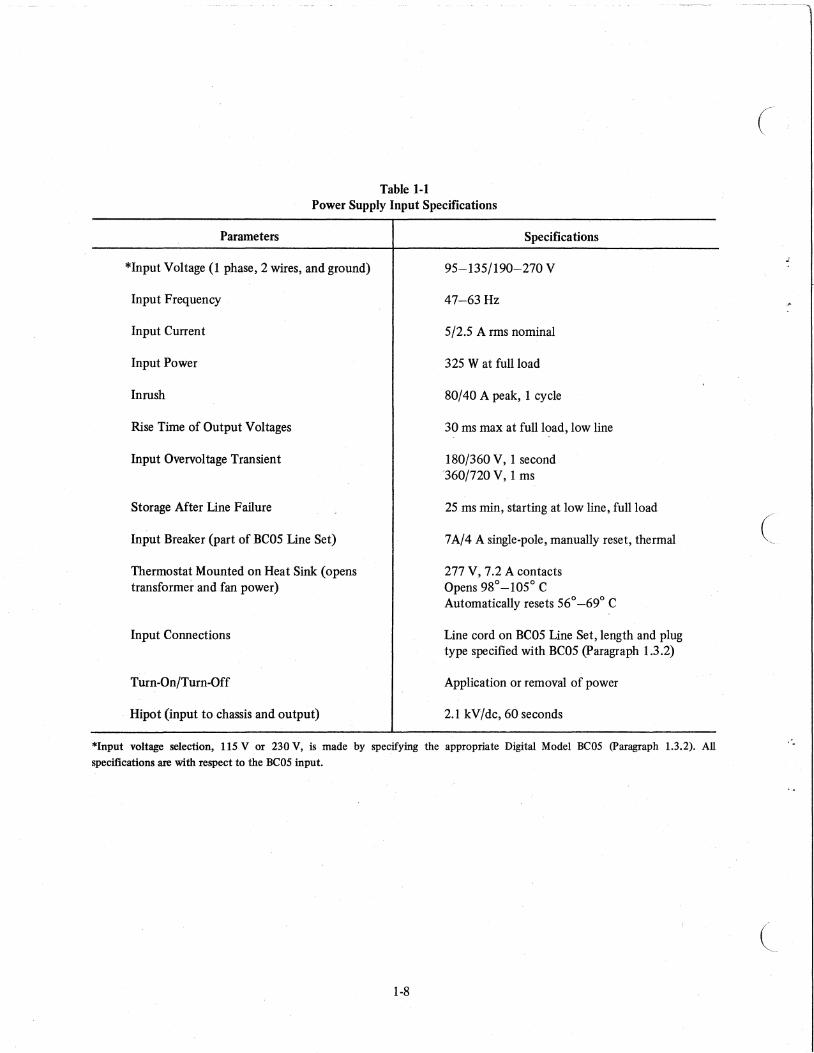
Table 1-1 Power Supply Input Specifications
Parameters
*Input Voltage (1 phase, 2 wires, and ground)
Input Frequency
Input Current
Input Power
Inrush
Rise Time of Output Voltages
Input Overvoltage Transient
Storage After Line Failure
Input Breaker (part of BC05 Line Set)
Thermostat Mounted on Heat Sink (opens transformer and fan power)
Input Connections
Turn-On/Turn-Off
Hipot (input to chassis and output)
Specifications
95-135/190-270 V
47-63 Hz
5/2.5 A rms nominal
325 W at fun load
80/40 A peak, 1 cycle
30 ms max at fun load, low line
180/360 V, 1 second '360/720 V, 1 ms
25 ms min, starting at low line, fun load
7 A/4 A single-pole, manually reset, thermal
277 V, 7.2 A contacts Opens 980 _1050 C Automatically resets 560 _690 C
Line cord on BC05 Line Set, length and plug type specified with BC05 (paragraph 1.3.2)
Application or removal of power
2.1 kVjdc, 60 seconds
*Input voltage selection, 115 V or 230 V, is made by specifying the appropriate Digital Model BC05 (paragraph 1.3.2). All specifications are with respect to the BC05 input.
1-8
(
l

(
(
:
c
Table 1-2 Power Supply Output Specifications
Load Range Static Dynamic
Parameter
Max Bypass Capacitance in load for 30-ms turn-on
Overload Protection
Current Limit @ 25° C
Backup Fuse
Adjustment Range
Regulation (all causes including line, load, ripple, noise, drift, ambient temperature)
Load Range Static Dynamic #1 Dynamic #2
Max Bypass Capacitance in load for 30-ms turn-on
Overvoltage Crowbar (blows fuse)
Current Limit at 25° C
Backup Fuse (series with raw dc)
Adjustment Range
Regulation Line Static Load Dynamic Load #1 DynamiC Load #2 Ripple and Noise 1000 Hour Drift Temperature (0-50° C)
I +15V
+5V
1·9
0-1 A 0-1 A
500 p.F
None
Specifications
1.3-1.7 A (-6.2 mAr C)
15 A (also used for +5 V)
±5%min
±5%
0-20 A ±5 A (within 0-20 A load range) No load - full load
2000 p.F
5.7-6.8 V actuate (7 V absolute max output)
24-29.4 A (-0.1 At C)
15 A
±5%min
±O.5% 3% ±2% ±1O% 4% peak-to-peak ±0.25% ±1%

Table 1-2 (Cont) Power Supply Output Specifications
Load Range Static Dynamic #1 Dynamic #2
Parameter
. M1lX~YP~SS Cap'acitllIlce illioalifor 30-ms tum-on
Overvoltage Crowbar (blows fuse)
Current Limit at 25° C
Backup Fuse (series with raw dc)
Adjustment Range
Regulation Line and Static Load Dynamic Load #1 Dynamic Load #2 Ripple and Noise 1000 Hour Drift
. Temperature' (0-50° C)
-15V
Specifications
0-7 A 61 = 5 A (0.5 A/#J.s) No load - full load (0.5 A/#J.s)
17.4-20.5 V (22 V absolute max output)
10-13.3 A (-0.03 At C)
SA
±s%rnin
±1% ±2.s% ±3% 3% peak-to-peak ±0.2s% ±I%
BUS DC LO L and BUS AC LO L Static Performance at Full Load
(for 230 V connection, double voltages below)
BUS DC LO L goes to high
BUS AC LO L goes to high
BUS AC LO L drops to low
BUS DC LO L drops to low
Hysteresis (contained in above specifications)
Output voltages still good
1-10
74-80 Vac line voltage
8-11 Vac above voltage at which BUS DC LO L goes to high
80-86 Vac line voltage
7-10 Vac below voltage at which BUS AC LO drops to low
3-4 Vac
70 Vac line voltage
c
... ------------- - -------
c
'.

(
c
Table 1-2 (Cont) Power Supply, Output Specifications
Parameter Specifications
BUS DC LO L and BUS AC LO L (Cont)
Worst case on power-up is high line, full load
Worst case on power-down is low line, full load
Open Collector
Pull-Up Voltage on Unibus
Rise and Fall Times
Dynamic Performance
~r----------------------------POWER ON
1 1 -. ______________ -:-____ SLOWEST OUTPUT
~' I COMES Up,
: I I 1
1 l- 30mS....l
MAX! f"'1--------------- BUS DC LO L
L2ms-: I'""MIN r----------- BUS AC LO ,L
U. ms NOMINAL 11-1094
~~i-----~--____________________ POWER DOWN
1
I 25 I~ ~I.~______ ms ______ ~.1 1 MIN FASTEST, D,UTPUT I GOES DOWN 1 1
~5m~ I M1N1!-. ----------------,...;....----- BUS AC LO L
1 1
BUS DC LO L 11- 1099
Output Characteristics
1-11
50 rnA sinking capability +0.4 V max offset
5 V nominal, 180 n impedance
1 J.l.smax Outputs shall remain in 0 state subsequent to power failure until power is restored despite Unibus pull-up voltages remaining

Table 1-2 (Cont) ( Power Supply Output Specifications .
Pammeter Specifications
POWEROKL
If output connector pin J2-11 is jumpeted to pin J2-14, an alternate AC LO L signal is available on pin J2-15. The static and dynamic performance characteristics are the same as stated above for AC LO L.
Load Impedance Low State
High State
'Output Impedance
Open Circuit Voltag~
Rise and Fall Times
Load May B~ Active
Short Circuit Current (to ground)
POWER
5-30 mA FROM +5V
SUPPLY 1 J 2- 8 o-t---+-----.------o ME ASUR EM EN T
COMMON .J2-2
POWER SUPPLY
J2-8
J2-2 COMMON
~
500.0. ±10%
-15V ±5%
POINT WITH RESPECT TO COMMON
500.0. ±10%'
MEASUREMENT POINT WITH RESPECT TO COMMON
-15V±5%
1-12
105 n max
0- 2.1 mA TO COMMON
+3.5 to +5.5 V (True) -1 to +0.5 V (False)
1 p.smax
o to +5.25 V max
165 rnA max
11-2023
(
l
".

._--- . -----_.-. -
Table 1-3 Mechanical and Environmental Specifications
Parameter
Weight DC Regulator Power Chassis Assembly including DC Regulator Module
Dimensions
Cooling Means
Minimum Cooling Requirements
Rated Heat Sink Temperature
Shock, Nonoperating
Vibration, Nonoperating
Ambient Temperature
Relative Humidity
Altitude
Specifications
7lb approximate 24 lbl approximate
3.5 in. height 19in.width 8 in. depth
Integral 3 in. fan (cover required over heat sink to plenum air)
375 CFM through heat sink 250 CFM over caps, chokes, and transformer
40 G (duration 30 ms) 1/2 sine in each of six orientations
1.89 G rms average, 8 G peak; varying from 10 to 50 Hz, 8 dB/octave roll-off 50-200 Hz; each of six directions
00 to +600 C operating -400 to 71 0 C storage
95% max (without condensation)
10Kft
1-13


2.1 INTRODUCTION
CHAPTER 2 INST ALLA TION
The H740D Power Supply is completely contained in an enclosed box with only the ac line cord, the circuit breaker reset button, and the dc output connector accessible from without. Before ordering the H740D, the customer should consider the dc voltage levels and power requirements of the device or devices that are to be powered by the H740D. The customer should then consider the space, environment, power, and cable requirements of the H740D. The following paragraphs provide that information, as well as information on inspecting, mounting, connecting, and turning on the power supply.
2.2 POWER SUPPLY CONFIGURATION
The H740D is available in 11~ V and 230 V configurations. The only difference between the two configurations is the type of line set installed. The BCOsH Line Set is installed for 115 V operation, the BCOs] Line Set is installed for 230 V operation. The customer must specify the line set desired when ordering the H740D.
2.2.1 Space Requirements
The H740D only oc.cupies a space 3·1/2 in. high X 19 in. wide X 8 in. deep.
2.2.2 Environmental Requirements
H740D environmental requirements are listed in Table 1·3.
2.2.3 Power Requirements
The H740D ac input power source must be capable of providing at least 325 W of 47-63 Hz ac power. The power supply is equipped with a 6·ft, 3·wire line cord and a 3·prong plug. The prime power ac input wall receptacle must be the same type as the line cord plug. Refer to Figure 2·1 for H740D connector specifications.
2.2.4 Cable Requirements
The H740D outputs are available at a Is·socket Mate·N·Lok connector accessible from the rear of the power supply chassis. Due to the varying requirements of different customers with respect to outputs used and cable lengths required, the fabrication of an H740D interconnecting cable harness is left to the customer.
2.3 INSTALLATION PROCEDURES
The· procedures. presented in the follOwing paragraphs are provided to assist in inspecting, mounting, connecting, and turning on the H740D Power Supply.
2·1

BC05H MALE PLUG
(SINGLE PHASE)
BC05J MALE PLUG
(SINGLE PHASE)
P_:fGROUND _'--~.--GROUND NEUTRAL
OR RETURN~I. ~ X.) \.
~PHASE
CONNECTOR SPECIFICATIONS
MODEL NEMA* PLUG RECEPTACLE
NUMBER CONFIr,URATION DESCRIPTION POLES WIRES
DEC DEC PART NO. HUB BEL PART NO. HUBBEL
BC05H 5-15 115V, 15AMP 2 3 90-08938 5266-C 12-05351 5262
BC05J 6-15 230V, 15 AMP 2 3 90-08853 5665-C 12-11204 5662
* ADD P SUFFIX FOR PLUG ADD R SUFFIX FOR RECEPTACLE II -2017
Figure 2-1 H740D Connectors
2.3.1 Inspection
Before installing the H740D, inspect it and report any damage ~o the local Digital Sales Office. Inspect as follows:
1. Inspect the chassis, line cord, and plug for damage.
2. Remove the top cover and inspect for loose or broken components, fan damage, cable damage, and loose nuts, bolts, screws, etc.
3. Inspect for proper seating of fuses and power connectors.
2.3.2 Mounting the H740D
The H740D can be mounted easily in any 19-in. equipment rack. Four bolts are used to attach the unit to the rack; it can be mounted within the rack or on the door. The H740D comes equipped with a 6-ft ac power cord. If a longer cord is desired, the desired length must be stipulated when ordering the power supply.
CAUTION Ensure that the H740D is installed so as not to obstruct the cooling fan intake vent as this may cause overheating.
2.3.-3 AC Power Connection
The H740D is equipped with a 3-prong connector which, when inserted into a properly wired outlet, grounds the power supply chassis. Due to normal leakage current from the power supply flowing into metal parts of the chassis, it is unsafe to operate the H740D unless the chassis is grounded properly. If the integrity of the ground circuit is questionable, the user is advised to measure the potential between the chassis and a known ground with an ac voltmeter.
2-2
(I
c.

. '
,( "--.
2.3.4 Initial Power Tum-On
Before connecting any devices to the H740D dc outputs, perform the following procedure:
CAUTION Verify that ac primary input power is compatible with the H400 Power Control Box installed in the H740D. Power requirements are indicated on the rear of the ppwer supply chassis .
I. Plug in the ac power cord and check for proper dc voltages at the IS-socket Mate-N-Lok coi:mectbr. Voltages should read as labeled on the rear of power supply chassis.
2. If any dc output voltages are incorrect, perform maintenance on the,H740D before continuing with this procedure. Maintenance procedures are provided in Chapter 4.
3. Check cooling fan operation. Verify that the fan is moving freely and that air flow is in the proper direction (fan draws air into chassis).
4. Unplug ac power cord.
2.3.5 Connecting the H740D to the Device
Interconnect the H740D and the device in accordance with the follOwing procedure:
1. Using the interconnecting cable harness (fabricated by the customer), connect the required power supply outputs to the device. Refer to the device maintenance manual to determine the dc voltages and control signals required for device operation.
NOTE If the PWR OK L output is to be used as an alternate AC LO L signal, a· jumper wire must be connected between pins 11 and 14 of the dc output connector on the rear of the power supply chassis.
2. Plug in the H740D ac power cord.
2-3


c
c
CHAPTER 3 PRINCIPLES OF OPERATION
3.1 INTRODUCTION
The power supply (Figure 3-1) can be divided functionally into five parts:
a. the line set, which adapts the power supply to 115 or 230 Vac input power and provides overload \
protection;
b. the thermostat, which provides overtemperature protection;
c. the fan, which provides forced air cooling;
d. the transformer, which steps the ac input voltage down to the level required by the dc regulator module;
e. the dc regulator module, which converts ac inputs to regulated dc outputs and provides power fail and clock outputs.
SEE NOTE "-.
,---, I PHASE
I AC" I LINE INPUT /I SET
I NEUTRAL
I I L ___ .J
NOTE:
THERMOSTAT (NORMALLY
CLOSED)
The Line Set is not part of the H740D pawer supply and must be ordered separately. Order Model number BC05 H for 115V operation and BC05 J far 230 V operation.
POWER SUPPLY
FAN
TRANS-FORMER
(T1)
Figure 3-1 Power Supply Block Diagram
DC REGULATOR
MODULE
The following paragraphs provide detailed descriptions of the H740D components.
3.2 LINE SET
K
P DC VOLTAGE OUTPUTS
POWER FAIL OUTPUTS
CLOCK OUTPUT
//-/972
To adapt the power supply to 115 or 230 Vac input power,the line sets (BC05H for 115 V operation, BC05J for 230 V operation) use different jumper wire configurations on output connector J5 (see Figures 3-2, 3~3, and 3-4). The 115 V line set output connector is jumpered such that the two primary windings of transformer T 1 are connected in parallel to the 115 Vac input; the 230 V line set output connector is jumpered such that the two primary windings of transformer T1 ,are connected in series to the 230 Vac input.
3-1

For overload protection, the line set contains a single-pole thermal circuit breaker. The circuit breaker trips when ( input current becomes excessive (7 A, @ 115 V, 4 A, @ 230 V) and is reset by pressing the reset button on the rear of the power supply chassis.
3.3 THERMOSTAT
For excessive heat protection, the power supply is equipped with a thermostat that is mounted on the heat sink (Figure 3-2). The thermostat. opens one side of the primary power input circuit whenever the heat sink temperature rises to approximately 1000 C, thereby removing power from the power supply and the cooling fan. The thermostat automatically resets at approximately 630 C.
3.4 COOLING FAN
The H740D uses a 3 in. fan (Figure 3-2) to circulate air over the heat sink, capacitors, chokes, and transformer. The fan operates continuously as long as the power suppiy is energized. If the thermostat opens, power is removed from the fan as well as the power supply. The fan forces air through the heat sink at a minimum rate of 375 linear feet per minute and over the capacitors, chokes, and transformers at a minimum rate of 250 linear feet per minute.
3.5 TRANSFORMER·
The H740D uses a step-down transformer to reduce the 47 to 63 Hz line voltage to 28 Vac as required by the dc regulator module (Figure 3-2). The transformer has two primary windings and one secondary winding. As previously stated, jumper wires in the line set connect the primary windings in parallel for 115 V input and in series for 230 V input.
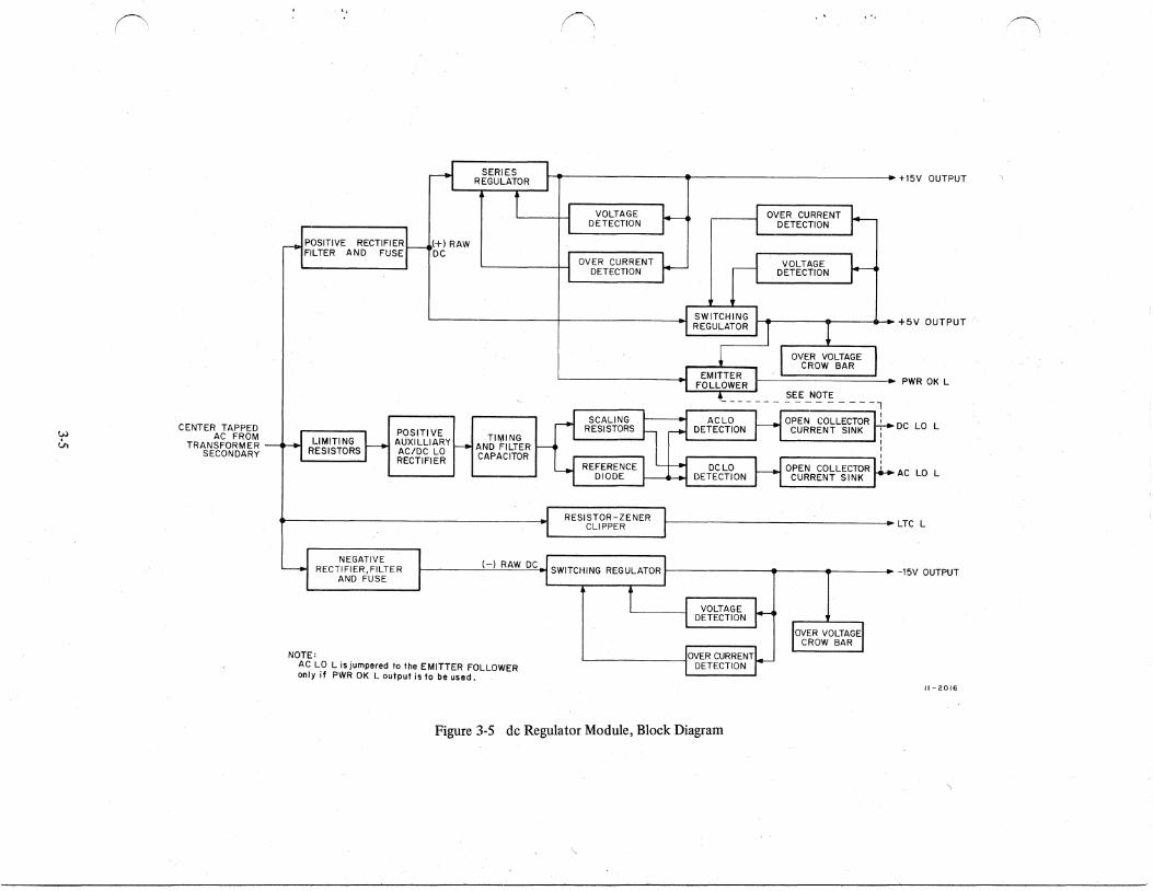
3.6 DC REGULATOR MODULE
A block diagram of the dc regulator module is shown in Figure 3-5. See engineering drawing D-CS-5409728-0-1 for the complete circuit schematic. The center-tapped output of power transformer T1 is applied to the rectifier and filter circuits. The rectifier circuits produce ±39 V nominal raw dc voltages which are unregulated but well filtered C by the input storage capacitor. _
The +39 Vdc is used to power two regulators: the +15 V regulator and the +5 V regulator. The +15 V regulator is a simple series regulator; the +5 V regulator is a higher powered, more efficient, switching regulator. Both regulators incorporate current limiting circuitry. The +5 V output is also protected against overvoltage by a crowbar circuit that limits the output to under 7 V; before the output gets to this value the crowbar circuit blows the fuse in the output circuit of the rectifier.
The - 39 V dc is used by the -15 V circuit, which is similar in operation to the +5 V regulator circuit. The -15 V crowbar circuit limits the output to -22 V.
The Clock signal (LTC L) is generated by a simple Zener clipper that is fed from the transformer secondary.
The AC LO L and DC LO L signals are used to warn the devices powered by the H740D and other deSignated devices of imminent power failure. Basically the transformer secondary voltage is detected and used to generate two timed TTL-compatible open-collector signals, which are used for power fail functions. These signals are Unibus (pDP-II bus) compatible.
The PWR OK L signal is used by some devices as an alternate to the AC LO L signal. The· PWR OK L circuit monitors the AC LO L output. When the AC LO L output is asserted, PWR OK L is asserted. However, AC LO L asserted places a ground directly on the output while PWR OK L asserted places a 100 n resistor tied to ground on the output.· Some devices may have power fail circuits which would be damaged if a ground were applied to them. These devices would use the PWR OK L output. Note that AC LO L must be jumpered to the emitter follower if the PWR OK L output is to be used. This signal is Omnibus (pDP-8 bus) compatible.
3-2

(
c
SEE NOTE 1
~ - -LINE SET
r- -115 VAC (C-UA-I
I
BC05H-0-0)
I I
AC { INPUT
I I L --
-
PHASE
GROUND
NEUTRAL
- -
- --r;3~ C LINE SET I (C-UA-
I I I I I L
BC05J-0-0)
PHASE
GROUND
NEUTRAL
- - -
- - - -, CKT BKR J5 J2
7AMP ~ 1 1
=i= 2 2
=i= 3 3
4 4
I 5 5
6 6
- - -- _ ....
-- - -- -, CKT BKR ~ 4AMP ~ 1
~ 2
=i= 3
4 • 5
C r-~ '--
- - -_ ..
nJ3 r---I-I-r
II~ POWER
" J4 SUPPLY
ttL FAN
II II J5 J3
II II I 1
" II 2 2
1/ II 1/ 1/ - - - --II r,.R~FO;;;R :;y II (D-IA -700 8726- 0- 0) II J I PI II T1 /I 5 5 5
" -th
II 1 1 J 1 II
2
1/ 4 4
1 ~ 7 2
/I II 2 2
II 6 1 II 3 3 4
II ~ 8 3 IJ
t 3 ~
AC CABLE HARNESS (D- IA-7008810 -0 - 0)
L --- -- - -- -- -
NOTES: 1. The line set is not port of the H740D Power Supply and must be ordered as a
separate item. Order BC05H for 115V operation and BC05J for 230V operation. 2. J2-11 is Jumped to J2-14 if the PWR OK L output istobeused.
THERMOSTAT I (NORMALLY CLOSED)
I
51 I I I
I I !
i i ! I I
J 1 iJ2
2 13 .1 ,
1 2
3 9
I 5
I
6
4
7
8
REGULATOR BOARD
(E - IA- 5409728 - 0 -0)
J 1
3 II II
2 II II
9 II II
5 II I
II 1 II
II 6 II
I II
JUMPER I 4 II (SEE NOTE 2)- I
\ II
7 II II
8 II II
U
t DC CABLE HARNESS
D -1 A -7008811-0 - 0
J 2 r--
1
2
3
4
5
6
7
8
9
10
11
I 12
13
,,4
15
-
+15V OUTPUT
AC LO L OUTPUT
DC LO L OUTPUT
LTC L OUTPUT
PWR OK ENABLE
PWR OK L OUTPUT
11-1971
Figure 3-2 H740D Power Supply, Wiring Diagram
3-3
7A BREAKER
~~~----~~-.o-~---+-------+--~
RFI CAp'
THERMOSTAT MOUNTED ON
HEAT SINK
POWER SUPPLY
FAN
I
540972B 115V LINE PLUG
¢ ~
DC REGULATOR
230V LINE PLUG
RFI CAP.
I
Figure 3-3 115 V Connection, Simplified Schematic Diagram
4A BREAKER
RFI CAP.
RFI CAP.
THERMOSTAT FAN
MODULE
I I I
11-2014
iEDC I REGULATOR I MODULE
I I I
L-______ ----------------l 1 11- 2015
Figure 3-4 230 V Connection, Simplified Schematic Diagram
3.6.1 Generation of Raw DC Voltages
As !ltated, the center tapped transformer secondary voltage is rel(tified and fIltered prior to being fed to the three dc regulators. The circuitry which accomplishes this is shown in Figure 3-6; Bridge rectifier D14 rectifies the ac and capacitors Cl and C2 fIlter the dc and maintain voltage for at least 25 ms when the input power is turned off or fails. Fuses Fl and F2 protect the regulator and load during fault conditions. Normally,the fuses will not blow when a regulator output is shorted because the three outputs are electronically overcurrent protected. However, the appropriate fuse will blow in the event of a +5 V or -15 V overvoltage crowbar or a failure in one of the overcurrent circuits. The resistors across the fuses provide a slow discharge (100-150 seconds) when power is turned off after a ( fuse blows. The capacitors are placed ahead of the fuse to limit the energy in the event of a fault and thus better protect the outputs.
3.6.2 LTC L Circuit
The Clock signal (Figure 3-6) is generated by a Zener clipper circuit. The output waveform is a square (clipped sine) wave at line frequency. For the positive half of the output sine wave, D13, clips at about +3.9 V; for the negative half, D13 clips at its forward voltage of -0.7 V.
3-4
(
(
w &.
(---->
CENTER TAPPED AC FROM
TRANSFORMER SECONDARY
'.
POSITIVE RECTIFIER FILTER AND FUSE
.(+) RAW DC
POSITIVE AUXILLIARY AC/DC LO RECTIFIER
NEGATIVE RECTIFIER,FILTER
AND FUSE
NOTE:
TIMING AND FILTER CAPACITOR
(--) RAW DC
AC LO L isjumpered to the EMITTER FOLLOWER only if PWR OK L output is to be used.
(\ ... ~
I •• • +15V OUTPUT
VOLTAGE DETECTION
OVER CURRENT DETECTION
RESISTOR-ZENER CLIPPER
OVER CURRENT DETECTION
VOLTAGE DETECTION
I • • •• +5V OUTPUT
OPEN COLLECTOR CURRENT SINK
OPEN COLLECTOR CURRENT SINK
PWR OK L
DC LO L
AC LO L
~---------------... LTC L
• • • -15V OUTPUT
11-2016
Figure 3-5 dc Regulator Module, Block Diagram
,
~\)

28VAC 47-63Hz
FROM TRANSFORMER
SECONDARY
NSS-3514
R45 4.7K 1/2W
~_-"----d" p ____ +.::..:39:...:V_ TO+ 5V REGULATOR CIRCUIT
.-____ +-~~_.__<~CL OUTPUT
~ TO AC LO
AND DC LO CIRCUITS
R44.7K 1/2W
D13 IN748A 3.9A
L..-_________ -:-,---____ -+-_cf'\..J>-~-+..:.39=-V=----.TO -15V REGULATOR CIRCUIT
11-1746
Figure 3-6 Rectifier and LTC L Circuits
3.6.3 AC LO L and DC LO L Circuits
The circuitry shown in Figure 3-7 is employed to generate the timed Unibus power status signals AC LO L and DC LO L. These signals are used for power fail functions. The transformer secondary voltage is rectified by 01 and 02 and ftltered by C9 and RI, R14. Circuit parameters are chosen so that the voltage across C9 rises slower than the
(
three regulated· output voltages on power-up and decays faster than the three regulated output voltages on C power-down. Two differential amplifier circuits are used to detect power status: Q17, Ql8 generate OC LO L; and Q15, Ql6 generate AC LO L. The differential amplifiers share a common reference Zener diode 03, which is fed approximately I rnA by R3. As C9 charges subsequent to power-up, first Q17, Ql8 and then Q15, Ql6change state; the reverse is true during power-down. When C9 starts to charge, Ql7 and Ql6 are on and Ql5 and Ql8 are not
.c0nducting. As C9 charges further, Q18 starts to conduct into R7 and raises the voltage on the cathode of 03. This acts as positive feedback and snaps Q 17 off and Q 18 on more solidly. A few milliseconds later, the voltage across C9 has risen sufficiently for the same process to take place in differential amplifier Q15, Q16.
':, Dl IN4004
,"VAC,4>-O,", '''" { TRANSFORMER SECONDARY D2
IN4004
AC LO L J2-1 OUTPUT >----100---...,
R13 470
Rl lK 1%
R14 lK 1%
R2 10K 1%
R12 10K 1%
R7 IK1%
Figure 3-7 AC LO Land OC LO L Circuits
3-6
, ~'
C9 2Ol£F
5%
R6 ~ 10K 1% + 11. 4 V
J2-6 DC LO.L OUTPUT
11- 2019 (
-

The status of each differential amplifier is followed by· the germanium transistor open-collector output stages Q19, Q20 for DC LO Land Q13, Q14 for AC LO L. These stages clamp the Unibus at about +0.4 V until the differential amplifier circuits sequentially signal them across Rll and R12 that power is up. The outputs then rise to about +5 V as dictated by the Unibus loading and pull-up termination resistors.
The sequence is as follows:
power up -+ then BUS DC LO L = 0 -+ then BUS AC LO L = 0 0= high (+3 V)
power down -+ BUS AC LO L = 1 -+ BUS DC LOL = 1 1 = low (+0.4 V)
Whenever DC LO L or AC LO L go low, there is sufficient storage in capacitors Cl and C2 to maintain output voltage long enough to permit the power fail circuit to operate. The open collector stages are designed to clamp the Unibus to 0.4 V maximum, even when there is no ac input to the regUlator. They are inherently biased on by Rll and R12 until the differential amplifiers signal that power is OK.
3.6.4 PWR OK L Circuit
The circuit shown in Figure 3-8 monitors the AC LO L output. When using the PWR OK L output, AC LO L must be jumpered to the base of Q12. In normal operation, AC LOL is floating and the +15 V and +5 V regulated outputs are present, hence Q12 is conducting. When Q12 is conducting, the PWR OK L output is negated (high). If AC LO L is asserted (low), Q12 turns off and PWR OK L is asserted (low). Note that AC LO L asserted places a ground on the output of the AC LO L circuit, while PWR OK L asserted places a 100 n resistor tied to ground on the output of the PWR OK L circuit.
REGULATED +15V
REGULATED +5V
AC LO L
3.6.5 +15 V Regulator Circuit
J2-7
R18 100 2W
Rl1 100
Q12 GPS A05
Figure 3-8 PWR OK L Circuit
PWR OK L
II -1973
The +15 V regulator shown in Figure 3-9 is a simple series regulator. The pass transistor Ql is a high-gain power Darlington and is mounted on the heat sink. Base drive current is supplied to QI via R38. Q3 acts to limit the value of this current to the required value by shunting it away from the Ql base. Q4, the voltage detector amplifier, biases on Q3 and thus limits current to Q1. The +15 V output voltage is sampled on the viewing chain R34, 35, 36 and compared to the voltage across reference Zener D8, which is fed by R37. If the output should try to increase from the regulated value, the emitter of Q4 is made relatively more negative than its base and conduction through Q4 increases. This increases the conduction through Q3 and causes QI to shut down sufficiently to restore the output voltage to the regulated value. Ambient temperature compensation of the voltage detector is essentially flat since D8 has a +2 mVt C temperature coefficient and the base emitter junction of Q4 has a -2 mVt C temperature coefficient.
3-7

....---~-_ TO PWR OK L CIRCUIT
+39V FROM RECT I F I ER --e--~\Mr---4"'---,,""'" r-~.--_____ -e-.,.-::-____ ...... _ ....... --=J.:2....:-5=<+15V,IA OUTPUT 08
XA55
R38 10K
R56 10K
R34 383 1%
C18 680PFI
R35 100
lN753A + CHi 6.2V R37 22pF
R36
464 1%
35V
Figure 3-9 + 15 V Regulator Circuit
11-2018
R35 acts as the +15 V voltage adjustment potentiometer. C18 is a high frequency stabilization capacitor. 02 is the overload detector; when the output current reaches 1.5 A nominal, the voltage across R33 is sufficient to cause 02 to conduct. This removes base drive from 01 and causes the regulator to current limit.
3.6.6 +S V Regulator Circuit
The +5 V regulator is similar to the +15 V regulator in that the sampled output voltage is compared to the voltage across a reference Zener by a voltage detector transistor, which in turn controls the drivers for the main pass transistor. The +5 V regulator circuit is shown in Figure 3-10. An over current circuit is likewise employed.
R41 0.025 7W,3%
R40 5.1
R39 5.1
R16
330
C17
6.B,uFT 35V R44 330
Q6 2N5302
10
Q8 XA55
Ll· 100"H
A 20A 01O,20A FAST RECOVERY
R47 6BK
R52 0.1 5W
R49 147 1 %
CW R50
R51 100
3% P.T.C.
100
Figure 3-10 +5 V Regulator Circuit
3-8
C7 6000
l"F,IOV
Ql1 C32AX135
011 lN5624
C
TOPWR OK L CIRCUIT
012 IN752A, 5.6V
R54 10
CB 0.22J1F
11-2020
-.
c

c
(
The viewing chain consists of R49, 50, 51 and the reference Zener, D9, which is fed by R44. QI0 is the detector amplifier. The pass transistor Q6 and first stage driver Q7 are mounted on the heat sink. The pre driver Q8 is turned on by R46. The current is diverted from the base of Q8 by off-driver Q9, which is controlled by QI0. The +15 V and +5 V regulators are similar in operation, i.e., a tendency for the output voltage to rise results in more conduction through Q lO and resultant limiting of conduction through Q6.
Here the similarity ends. The +5 V circuit is a regulator that operates in the SWitching mode for increased efficiency. To get the r_egulator to switch, positive feedback is applied to the voltage detector input via R47. Thus the whole regulator acts as a power Schmitt trigger and is either completely turned on or turned off, depending on whether the output voltage is too high or too low. When Q6 is on, it supplies current through fllter choke L1 to the output smoothing capacitor C7 arid the load. When Q6 is off, the Ll currf:nt decays through commutating diode DlO, which becomes forward biased by the back EMF of L1. The waveform across DlO is a 30 V nominal rectangular pulse train. The flltered output across C7 is thus +5 V with about a 200-mV peak-to-peak, lO-kHz nominal sawtooth of super-imposed ripple. At the crest of the ripple, Q6 turns off, at the valley, Q6 turns on. This switching mode of operation limits the diSsipation in the circuit to the saturate4 forward losses of Q6 and D 1 0 and the switching losses of Q6. The resultant high efficiency allows the heat sink to be small and', reduces the number of power semiconductors required.
R50 is the voltage adjustment potentiometer. R51 is a positive temperature coefficient wire-wound resistor that compensates for the fact that the QI0 base-emitter junction and the reference diode D9 both have negative voltage temperature coefficients. Q5, current limited by R39, 40, detects the overcurrent signal generated across resistor R41, which is in series with the Q6 collector. .;
Output fault current is limited to a safe value because conduction of Q5 makes the reference voltage across D9 decrease to zero. This causes QI0 to conduct and shuts down th~ regulator. C5 is an averaging capacitor, which is necessary in the circuit because the current through R41 is pulsating.
High frequency bypass capacitors, C3 and C6, are used on input and output of the regulator, respectively. C4 is used to slow down theturn-ort of Q6 to allow DI0 to recover from tHe on state without a large reverse current spike.
In the event that a malfunction causes the output voltage to increase beyond about 6.8 V nominal, Zener diode D 12 will conduct and fire silicon-controlled rectifier Q 11. This will crowbar the output voltage to a low value through Dll and will blow fuse Fl in the rectifier circuit through R52.
3.6.7 -15 V Regulator Circuit
The -15 V regulator circuit is shown in Figure 3-11. It is essentially the complement of the +5 V regulator circuit and differs only in minor detail.
The crowbar device is a Triac Q27 instead of an SCR; no temperature compensating resistor is required because Q26 and D4 track each other, as in the +15 V regulator; the detailed intercoimection of the drivers and the circuit values are different. The -15 V output voltage is adjusted by potentiometer R26.
3-9

ClO r--39V I"F FROM J2-2 GROUND \ RECTIFIER
R29 R28 .. R27 OUTPUT
lK 4.7K 464 R31 C15
1/2W 1% 100 0.22~F 50V
R26 100 1I2W
C13 C14 04 R24 lJlF
3000!,F 6.2V 25V lN753A 68K
R25 R57 383 05.20A 10K 1% FAST 1 3 RECOVERY Q27
MACI1-3 2
Cll o.033!'F R30
100V 10
C12 2.2,.,.F 35V
+ R22 0.2 5W ?~5k~~B
Q21 XA05
06 IN5624
R20 L'2 10 tOO~H
R19 lOA J2-9 -15V,7A
0.06 C 0 OUTPUT
5W 3%WW 11-0970 (-
Figure 3-11 -15 V Regulator Circuit
c 3-10
(
(
4.1 INTRODUCTION . .' . . . . ':" '. ", \'~. . .
This chapter contains power supply maintenance information consisting of adjustments, circuit, waveforms, and troubleshooting. The adjustments consist of three output potentiometers. The circuit waveforms provide a guide to pr()p'er()pera~i()n ~t various. pla<:es, in, the circuit. The, troubleshootings~f,!i0-A'Pr,9'1~~~.:.IJi!r,~!,J,lir-~~,' and' a troij~l~shoot~gchart.as,amaintenan'ce aid in isolating power supplyriialfUIl~tipris;;"'(~(>"~~':·!;r.:y ;.';/""::~:(i~'
4'~'~l}lUSWENis .' . :"""<
Th~i.etar~'qnly, thre~,adi~sfmentsto the power supply . These adjustPtetbtee' d~ Qutput v61tages:+1S' ,y,+~ V, 'and' -li~r.A smallscrewdrh:erjs all that is reqUired. Clockwise adjustrIlenl·?t\an,ofth~:P9tent!otp,¢~w~creases' volf~ail',,,:iii1dth¢'p6te~tiometers are located' on the top sideo(tpe dc;;'ii:p~;:,m~~'@i·i:~·;rh~:iipq~fftlometer
do~~'i'",:?' .. . ' '",Jii;~~~~l~~t~~~~~~~",,;l,~,,~ gZ:t,,;'~~1ff:~" c,' . ,
, ,
In performing any of these adjUstments note the following: '
CAUTION 1. Do not adjust voltages beyond their 105 percent rating and
'"adjust slowly to avoid overvoltage crowbar,wh~ . '1'4~JQW:j/ v;,'ii;t:i~
,<lcp~tp~tfuses. ' , or' ' ' i~;{0~;]~~~·~ti;/'1~l~k,;ii'~\;;J,;~mtl~~ '" '2.l)~a calibrate<l voltmeter, preferablyadigit1li\';~lhrt~;t~r,< " ", "/'
, VQltages~hould be adjusted to th~il;center,yalues~+15:Q", +5.0, al1d -J5.0, all un<ler load atth~:dcoutputcoim~ct6~ .
..•. . . ..~ ':'. :. ,.: .
,4.3" ' CIRCUIT ,W A VEfORMSi'rJf&~0,;'~~7';:~"t;,~,:::~i~;:~~i.'~!1~'i~;i~;;:~\$:ff ; Theiwo' s¥itchingregulator circuits used on the dc regulator mb,dule generad:":15V~lFlgur.eA~l' ,ows SIX
wav~formsof the +5 V regulator circuit,taken ,at two points (Aapd:tnin, ":·t,~~!~r¥~?~9};{,,\,,. ,; s~, b, and c are 'taken at point A, which is the +5 V cirCuit, Q6 transistor output:;: 'efuttri:s d;:e:; ah~ff melt' ,;.'at point B, which is +5 V power supply output. Figure 4-1 itlso indicates the load conditions and timescitles for each waveform. Figure 4-2 Shows six wavef()rms of the -J 5 V regulator' circuit taken at two points (Cand I» in the circuit (Figure 3-11 ).' Waveforms a, b,and, c are taken at pOintC, Which is the -15 V cirCuit, Q22 transistor. output. Waveforms d, e, and f are taken at point D, wruchis the -15 Vpower sUpply output. The load conditions and time scales of the respective waveforms are indicated ill Figure 4-2. These waveforms were taken, on a Tektrorux Model 453 oscilloscope; To locate the circuit test pOints on thedc regulator module, refer to engineering drawing E·IA-5409728~O-O.Allwaveforms are with respect 't()poVVersupply common .• ' i
4-1

a) Point A, No load, 2.ms Idiv, arid 10V/div.
b) Point A, No load, 20' pS!div, and
.10V/div.
c) Point A, 20A 10ild, 20 psldiv, and 10V/div.
d) PointB, No load~ 2 msldiv,.anCi 50 mV/div.
e) Point B, No load, 20 psldiv, and 50 mV/div.
f) Point B, 20A load, ps/div, and 50 mV/div.
Figure 4-1 +S V Regulator Circuit Waveforms
4·2
(
c

(
"
a) Point C, No load, 5 ms/div, and 10V/div.
b) Point C, No load, 50 Ms/div, and 10V/div.
cl Point C, 5A load, 50 )ls/div, and 10V/div.
d) Point D, No load, 5ms/div, and 50 mV/div.
eJ Point D, No load, 50 Ils/div, and 50 mV/div.
f) Point D, 5A load, 50 Ils/div, and 50 mV/d.iv.
Figure 4·2 -15 V Regulator Circuit Waveforms
4·3

4.4 TROUBLESHOOTING
Troubleshooting information for the power supply consists of troubleshooting rules, hints, and a troubleshooting chart. This information provides a maintenance aid to isolating power supply malfunctions (engineering drawing D-CS"5409728-0-1). ..
4.4.1 '. Troubleshooti~g Rules
Troubleshooting rules for the power supply are listed as follows: . .tII :
_j\ -".," ~ v
a; Ensure that power cord is unplugged before servicing the power supply. . .
. b. EnsUre that input capacitors CI and C2 are discharged before servicing the power supply. A 10 to 1.00 n, 10 Wresistor can be used to hasten the discharge of the capacitors. (Be sure power is off.)
c. The dc regulator module is not internally grounded to the chassis; therefore, shorts toground can be located.
d. The de output fuses Fl and F2 can be replaced without removing the dc regulator module. Before unsoldering fuses, observe cautions described in steps a and b.
e. For proper operation, all hardware must be secured tightly to about 12 in~/lb (i.e" capacitors, chokes, ·~emicondtictors). All hardware should be replaced with identical hardware replacement parts.
[ . Thede regulator module may 'be removed from the top of the power chassis assembly while the latter is still bolted to the cabinet. Thedcreguliltor module is held in place by six screws.
(
' .. g. .'. When replacing power semiconductor components that are secured to the heat sink, apply a tlti,n co~t of .(" Wakefield no. 128 compound or Dow silicone grease to the heat sink contact side (bottom) of the seniiconductor. Insulating wafers are not required.
4.4.2 Troubleshooting Hints
CAUTION Disconnect all power supply outputs.
, " . ..
The: most likely source of powe~.~upply malfunCtion isthedc regulator module. A quick remedy for a malfllllction maybe to replace the entire module. The problem, however, could be a short in the device connected to the power supply or possibly a.defective component in the power supply aCinput circuit.
The +5.V and ,..15 V regulators containovervoltage detection circuitry. If R50 or R26 is adjusted too fat clockwise, the corresponding crowbar circuit will trip and blow fuses. To correct this condition: adjust the potentiometer fully counterclockwise, replace the blown fuse, andre-adjust perParagrl.lph4.2.
Make a visual examination of the circuitry. Check for burnt resistors, cracked transistors, burnt printed circuit board . etch, oil leaking from capacitors,and loose connections. A visual check can be a quick method of locating the. cause of a malfunction.
4.4.3 Troubleshooting Chart
In checking the various areas of the power supply, the rules listed in Paragraph 4.4.1 should be followed. The waveforms shown in Paragraph 4.3 provide a comparison for the troubleshooting readings. Table 4-1 provides the de
, regulator troubleshooting chart;
4-4

c
< •
READER'S COMMENTS
H740D POWER SUPPLY MAINTENANCE MANUAL DEC·ll·H740A·A·D
, Your comments and suggestions will help us in our continuous effort to improve the quality and usefulness of
our publications.
What is your general reaction to this manual? In your judgment is it complete, accurate, well organized, well
written, etc.? Is it easy to use?
What features are most useful? -~------------------------------
What faults do you find with the manual?
Does this manual satisfy the need you think it was intended to satisfy?
Does it satisfy your needs? _________ _ Why? ~-------------------------------
Would you please indicate any factual errors you have found.
Ple.ase describe your position.
Name Organization
I Street _____________________ Department
~ I City _________ ___ State ___________ _ Zip or Country
'--

- -- -- -- -- - -- - - FoldHere - - - - -- -- -- -- ---
- - - - - - - - - DoNotTear-Fold Here and Staple - - - -- -- -- -- --I
BUSINESS REPLY MAIL NO POSTAGE STAMP NECESSARY IF MAILED IN THE UNITED STATES
Postage will be paid by:
Digital Equipment Corporation Technical Documentation Department 146 Main Street Maynard, Massachusetts 01754
FIRST CLASS PERMIT NO. 33
MAYNARD, MASS.
(
(
1-, r
< I

:
Problem
No +5 V and +15 V output
+5 V output too low
+ 15 V output too high
No -15 V output
-15 V output too low
AC LO L will not go high
AC LO L will not go low and/or acts erratically on Power-On/Power-Off
OC LO L will not go high
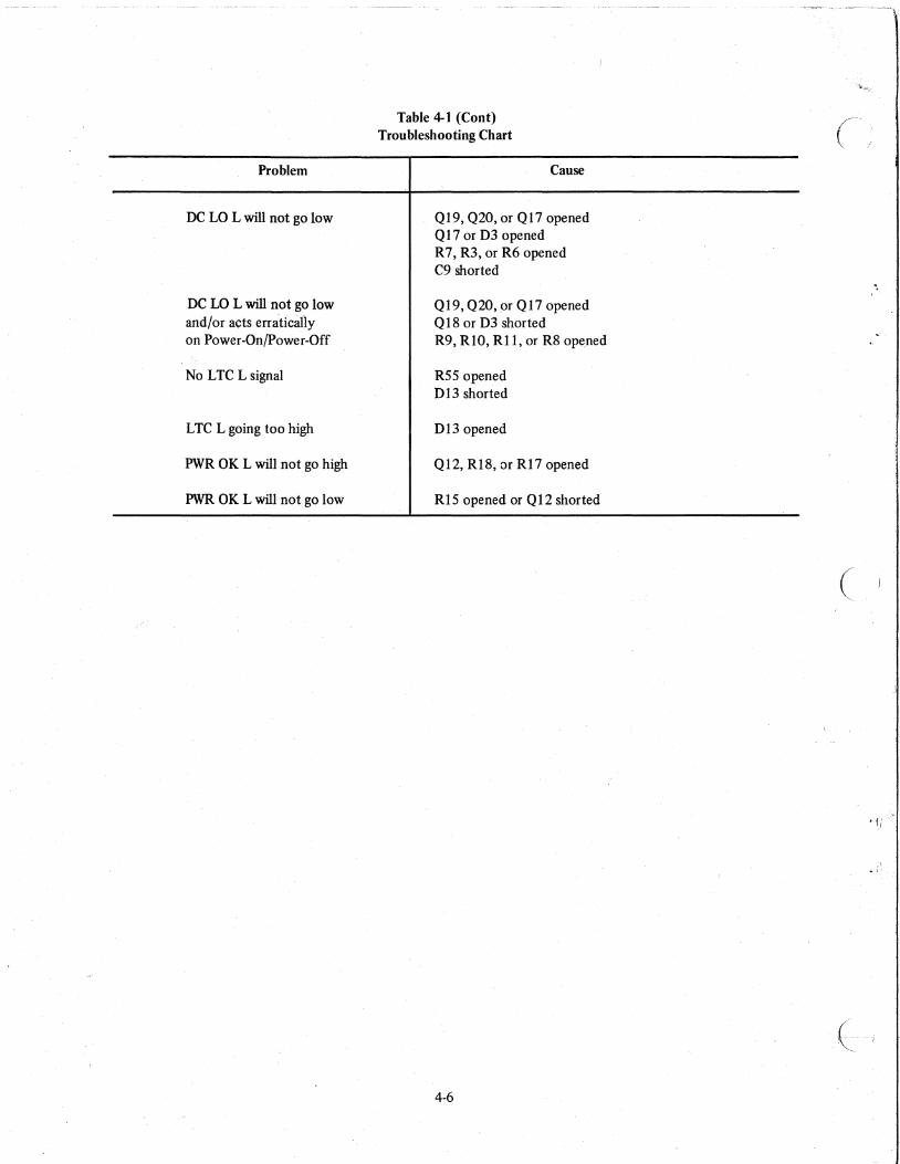
Table 4-1 Troubleshooting Chart
Flopened
Cause
014 or transformer opened +5 V adjusted too high*
Q5, 09, QI0, Q9, Qll, 012, or 010 shorted C5 or C7 shorted R49, R50, R46, or R44 opened
Q6, Q7, Q8, or Oil shorted A9, QIO, or 09 opened*
R51, or R50 opened
Ql shorted £8 opened R35 or R36 opened
F2 opened 014 or transformer opened -15 V adjusted too high *
Q25, 04, Q26, Q21, Q27, 07 or 05 shorted C14 or C12 shorted R22, R26, R25, R29 opened
Q22, Q23,Q24, orD6 shorted Q25, Q26, or 04 opened R26 or R27 opened* -15 V adjusted too high *
Q13, Q14, or Q15 shorted Q16 or 03 opened R7, R3, R6, or R8 opened C9 shorted
QI3,Q14, or Q16 opened Q 15 or 03 shorted R12, RI3,R7, or RIO opened
Q19, Q20, or Q12 shorted Q 17 or 03 opened R 7, R2, or R6 opened C9 shorted ..
* This set of causes makes the crowbar iue, which in tum blows the appropriate fuse.
4-5
Problem
DC LO L will not go low
OC LO L will not go low and/or acts ernitlcally on Power-On/power-Off
No LTC L signal
LTC L going too high
PWR OK L will not go high
PWR OK L will not go low
Table 4-1 (Cont) Troubleshooting Chart
Cause
Q19, Q20, or Q17 opened Q 17 or 03 opened R7, R3, or R6 opened C9 shorted
Q19, Q20, or Q17 opened Q 18 or 03 shorted R9, RIO, Rl1, or R8 ope.ned
R55 opened 013 shorted
013 opened
Q12, R18, or R17 opened
R15 opened or Q12 shorted
4-6
... ;:1


digital equipment corporation