Embed Size (px)
Citation preview

GSM/ EDGE Mobile Technology Power Amplifier Characterization
Matthew Angert Masters Thesis – First Draft
March 5, 2004
I. Introduction ................................................................................................................... 3
II. Background .................................................................................................................. 4
A. Power Amplifier Characteristics................................................................................ 4
B. I-Q Modulation........................................................................................................... 5
C. Encoding Data in GSM and EDGE: .......................................................................... 6 1. Encoding Data in GSM........................................................................................... 6 2. Encoding Data in EDGE......................................................................................... 6
D. GSM/ EDGE Signal Structure.................................................................................... 9
III. Measurement Theory............................................................................................... 12
A. Power Added Efficiency – ........................................................................................ 13
B. Power versus Time Measurement............................................................................. 14
C. Error Magnitude Vector Measurement .................................................................... 15
D. Output RF Spectrum - Adjacent Channel Power ..................................................... 18 1. Output RF Spectrum due to Modulation and Wideband Noise ............................ 19 2. Output RF Spectrum due to Switching Transients ............................................... 19
IV. Measurement Implementation ................................................................................ 21
A. Overview of Testing.................................................................................................. 21
B. Power Amplifier Module Evaluation Boards ........................................................... 22
C. Implementation - Power Added Efficiency............................................................... 23
D. Implementation of Tests Using Vector Signal Analyzer........................................... 23
E. Implementation of Tests Using PSA Spectrum Analyzer.......................................... 27
F. Biasing the PA .......................................................................................................... 28
G. PSA Testing - Automated Testing Codes written in Agilent Pro VEE ..................... 33
V. Results for VSA Measurements ................................................................................ 38
A. Power Added Efficiency Results............................................................................... 39
B. Power versus Time ................................................................................................... 40
C. EVM Measurements ................................................................................................. 41
D. ORFS - Spectrum due to Modulation....................................................................... 43

E. ORFS - Spectrum due to Switching .......................................................................... 44
G. Results of VSA Showing Dynamic Range as an Issue:............................................. 45
VI. Results for PSA Measurements............................................................................... 46
A. Power versus Time Results....................................................................................... 47
B. EVM Measurements.................................................................................................. 48
C. ORFS - Spectrum due to Modulation ....................................................................... 49
D. ORFS - Spectrum due to Switching.......................................................................... 52
VII. Conclusions.............................................................................................................. 54
VIII. References .............................................................................................................. 56

I. Introduction
In United States Code Division Multiple Access (CDMA) technology is primarily used for cellular phones, but worldwide Global System for Mobile Communications (GSM) (or Groupe Speciale Mobile) is the most widely deployed wireless network. Worldwide GSM Mobile Phone Users Soon to Reach 1 Billion, GSM Group Says The GSM Association, an industry association promoting GSM mobile phones, announced that worldwide users of GSM mobile phones have reached 970.5 million.1
GSM is only second generation (2G) meaning it older and has limited data rate and capability. The Enhanced Datarates for GSM (also abbreviated with Global 2 (EDGE) is third generation (3G) (some call it 2.5G indicating it is more advanced than 2G technology but not quite as high data rate as a 3G system). EDGE uses much of the same network as GSM. EDGE is viewed as a stepping-stone that more of the infrastructure can be reused and thus cost is diminished.
To utilize the enhanced features of EDGE, better components (ie. power amplifiers) need to be developed. Along with the better components new measurement techniques need to be developed and implemented to ensure the quality of the new EDGE components.

II. Background A. Power Amplifier Characteristics
The final stage in a RF front end before the antenna is usually a power amplifier (PA). The PA creates a large output power from the small input power signal to be sent out to the antenna. Many issues arise in power amplifiers due to their distortion, large power consumption, and high cost of these devices. Because of these issues, characterizing and minimizing the negative effects of power amplifiers are of utmost concern in mobile telephone design. The PA is usually integrated into a power amplifier module, which consists of filters to use multiple bands, some sensing loops, matching components, etc. 3As more and more components are being pushed to become integrated on a single chip, the PA cannot be integrated with the rest of the transceiver because of the high amounts of power needed to run these devices. Linearity and harmonics - Ideally we want the transfer function of a power amplifier to be linear over the entire input range for all desired outputs. All realistic amplifiers have a limited linear range and outside this range output saturation and distortions occur as shown in Figure 1. Many times a larger issue is that the non-linear characteristics cause harmonics of the input signal to be created at the output. These harmonics can cause interference in other frequency channels and could also mix in the receiver to create distortion at the frequency of interest. 4
Figure 1. Output Power versus Input Power showing distortion and compression characteristics of transfer function of PA.

B. I-Q Modulation
A signal that has been modulated by a carrier can be represented by ( ) cos( ( ))cA t t tω θ+ . To make a signal have more efficient bandwidth usage, quadrature
amplitude modulation (QAM) can be employed. If two signals are to be transmitted, m1(t) and m2(t), they can be sent by having the carrier frequency 90 degrees out of phase of each other. Using the same local oscillator, the signal is delay by 90 degrees, the cos( )ctω is modulated with m1(t) and sin( )ctω is modulated with m2(t). The advantage of doing quadrature modulation comes from the fact that sine and cosine are orthogonal to each other. Even though both signals have the same center frequency and bandwidth, they do not interfere because of this orthogonality. Therefore two signals can occupy the same bandwidth that one signal would occupy if it did not use quadrature modulation. 5
Quadrature amplitude modulation is used in GSM and EDGE. All QAM transmitted signals can be represented as:
1 2( ) ( ) cos( ) ( ) sin( ) c cx t m t t m t tω ω= + where m1(t) and m2(t) are two separate message signals and wc is 2πfc
The in-phase portion of the signal is the one associated with the cosine and is denoted I(t). The quadrature portion of the signal, which is the one 90 degrees out of phase with the cosine signal, is denoted as Q(t). Therefore the signal can be written as:
( ) ( ) cos( ) ( ) sin( ) c cx t I t t Q t tω ω= +
The I(t) and the Q(t) can be plotted against each other to get a picture of the signal. This is known as an I-Q Diagram or constellation diagram. For example the EDGE I-Q diagram is shown in Figure 2.
Figure 2. I-Q Constellation Diagram of an EDGE Signal6

C. Encoding Data in GSM and EDGE: 1. Encoding Data in GSM
To understand EDGE modulation, first look at the simpler GSM modulation.
The modulation scheme used in GSM is Gaussian Minimum Shift Keying (GMSK). GMSK signals are generated by sending the signal through a Gaussian prefilter, which reduces the side lobes.7 Then the signal is encoded in the following manner. Four options are created: positive in-phase and quadrature components, positive in-phase component and negative quadrature component, negative in-phase component and positive quadrature component, and negative in-phase and quadrature components.
As the signal shifts phase, the I-Q position changes from one position to the next and this determine what bit is encoded. For example if the I and Q components are both positive at a certain point, by changing the signal to having negative in-phase component and positive quadrature component would encode a bit “1” as shown in Figure 3. As all the bits are encoded the signal shifts clockwise or counterclockwise to encode all the bits.
As can be seen from Figure 3 at every time the signal is a constant distance from the origin, which signifies that it always has constant amplitude. Because the GSM signal has constant amplitude, the design for components is simplified. Figure 3. Illustration of MSK 8 2. Encoding Data in EDGE
The modulation scheme used in EDGE is a variation on 8-Phase Shift Keying (8-PSK) called 3π/8 8-PSK. 8-PSK Modulation
In Phase Shift Keying the I-Q plane has many more positions that can allow the encoding of more bits at a time point. Having one or more bits being indicated by one sample of a signal creates symbols. By using 8-PSK the eight positions are used so that each sample indicates three bits. In this way the data rate to transmit the information is

increased from 1 bit per sample to 3 bits per sample comparing the GMSK to the 8-PSK modulation schemes. Again by changing position relative to the current position, the bits are encoded onto the carrier as shown in Figure 4.
An issue with 8-PSK is that in certain transition the signal crosses the origin of the I-Q diagram, which indicates that the amplitude is becoming zero. The amplitude becoming zero at any time causes problems in the amplifiers used because distortions occur. Also zero crossings result in discontinuities in envelope and phase of the waveform. Amplifiers have only a certain linear range and amplifiers can cause distortions when the signal is very small and is close to zero.
In EDGE, to avoid the amplitude become zero, 3π/8 8-PSK modulation scheme is used. In this scheme there are still eight possible destinations starting at each sample point, but they are each shifted so that at no time does the signal cross zero and shown in Figure 5. 3π/8 equals 67.5º, which is amount of shift, that occurs between the present symbol and the adjacent symbol. Effectively the targets generated are like the 16-PSK modulation scheme. Looking at Figure 5, the targets switch from white to gray with each sample taken to encode the data onto the carrier. The bits are mapped into symbols using Grey Code, which means each adjacent symbol differs only by one bit.
Figure 4. 8-PSK Modulation9 Figure 5. 3π/8 8-PSK Modulation10
Therefore EDGE modulation scheme of 3π/8 8-PSK has the advantage of GMSK that it has no zero crossings and therefore does not cause distortions to the amplifier. The main challenge of 3π /8 8-PSK is that the signal no longer has a constant envelope. Because the signal no longer has a constant envelope, provides major issues for

components in particular, the power amplifier. With a constant envelope, the power amplifier’s linear range essentially needs to be zero because the signal’s amplitude does not change, but with EDGE’s 3π /8 8-PSK, the linear range needs to be large. As shown in Table 1, EDGE’s required linear range is quite significant.
GSM (GMSK Modulation)
EDGE (3π/8 8-PSK Modulation)
Peak-to-average ratio 0 dB 3.2 dB Peak-to-minimum 0 dB 17 dB
Table 1. GSM and EDGE peak to average and peak to minimum ratios11

D. GSM/ EDGE Signal Structure GSM and EDGE both use Time Division Multiple Access (TDMA) and Frequency Division Multiple Access (FDMA). The TDMA signal is broken up into eight equal time slots, which repeat in what is called a frame as shown in Figure 6. Figure 6. TDMA signal with 8 repeating timeslots. GSM and EDGE use a signal with a 200 kHz bandwidth for each carrier. The frequency bands used for GSM EDGE include: Frame Structure:
The frame and timeslot structure is shown in Figure 7. Each timeslot is 576.92 us and therefore a frame is 4.615 ms. Within each timeslot tail bits are at the beginning and end of each slot. These are included to tell when the signal starts and stops. Then the actual data is contained next, which included two control bits and a midamble in between. The midamble contains information about the burst such as what data rate is being used, etc. At the end of each timeslot there are guard bits, which simply add a buffer between this slot and the next. Because the signal is on only during its intended time and off in the others it is known as a burst. In this one timeslot is where one user transmits, or receives, the signal.
During the timeslot other types of bursts can be transmitted including a frequency
correction burst, synchronization burst, and dummy burst. The frequency correction burst corrects for frequency errors during transmission. Synchronization bursts make the time slots begin and end at the correct time as time delays can occur during transmission. A dummy burst is a burst that is just blank.12
Figure 7. GSM and EDGE Burst Structure13

The Figure 7, which is GSM’s burst structure, shows the timeslot of 577 us containing 156.25 bits. In EDGE’s case the same structure can be used but consider each bit as a symbol. Only in the Data portion of the timeslot does the symbols equal 3 bits per symbol; in the rest of the burst each symbol is still 1 bit. Therefore the number of symbols in the timeslot would be 156.25 symbols. Not counting the guard bits, gives 148 symbols, which is known as the “entire burst”. Not counting half a symbol of the front tail and half of a symbol of the end tail, gives 147 symbols, which is known as the “useful part of the burst.” Some refer to the burst as containing 142 symbols, which indicates that both tails are not included in the definition of the burst.
Because GSM and EDGE have the same time duration for a slot and have the same occupied bandwidth in frequency, GSM and EDGE signals can exist in the same frame. This compatibility provides designers with more freedom and flexibility in that systems can use EDGE, GSM, or both and change between the two depending on conditions. Figure 8 shows a frame with EDGE at two different power levels, GSM at two different power levels, and empty slot. Figure 8. GSM and EDGE versus time showing both EDGE and GSM coexisting14

GSM and EDGE both have a symbol rate of 270.833 kHz. GSM using GMSK modulation has 1 bit per symbol as shown previously. EDGE using 8-PSK has 3 bits per symbol and as shown in Table 2, higher data rate can be reached by using EDGE. GSM/ GPRS EDGE Modulation Bits/symbol Symbol rate Modulation Bit Rate Ratio Data Rate per time slot Data Rate per time slot (User Rate) Theoretical Max User Rate Data Rate per eight time slots (User Rate) Theoretical Max User Rate – Eight Slots
GMSK 1 270.833 ksym/s 270.833 kbps 22.8 kbps 14.4 kbps 20 kbps 115.2 kbps 160 kbps
3π /8 8PSK 3 270.833 ksym/s 812.499 kbps 69.2 kbps 48 kbps 59.2 kbps 384 kbps 473.6 kbps
Table 2. Summary of GSM and EDGE characteristics 15

III. Measurement Theory
1. Power Added Efficiency - Determines how well the power amplifier converts DC power into RF power.
2. Error Vector Magnitude – Determines the quality of the modulation and how
much modulation error has occurred.
3. Power versus Time – Determines the distortion of the waveform shape and the interference into other time slots.
Output RF Spectrum – Adjacent Channel Power – Determines the amount of interference into other frequency channels.
4. Spectrum due to modulation – Determines the adjacent channel power that comes
from the steady state component of the signal.
5. Spectrum due to switching – Determines the adjacent channel power that comes from the transient component of the signal.

A. Power Added Efficiency –
The end goal of a power amplifier is to take a weak RF input power and using the DC biasing of the circuit, create a strong RF output power. A good measure of performance of a power amplifier is therefore how efficiently this conversion is done. Power Added Efficiency is defined by the below equation:
Pout - PinPAE(%)= 100%Vsupply Isupply
(Equ 1)
where Pout is RF output power of PA in Watts, Pin is RF input power in Watts, and Vsupply and Isupply are the DC voltage and current of the source.
The Vector Signal Analyzer was used to measure the RF output power and the Electronic Signal Generator created the RF input power. Both of these quantities are in dBm so the correct equation becomes:
( ) ( )10 1010 10
10
Pout dbm Pin dbm
-PAE(%)= %Vsupply Isupply
(Equ 2)
where Poutm(dBm) is RF output power of PA in dBm, Pin(dBm) is RF input power in dBm, and Vsupply and Isupply are the DC voltage and current of the source. PAE Calibration:
To protect the VSA a 20 dB attenuator had to be added after the output of the power amplifier. This attenuator is not precisely 20 dB and the two adapters and two cables used for measurement provide some attenuation so this should be calibrated out to provide an actual measure of PAE. Running the setup over the maximum power levels of the ESG at the frequency ranges of interest, the attenuation of the 20 db attenuator, cords, and adapters totaled 22.0 dB. Therefore the final equation used to calculate PAE is:
( ) ( )22.010 1010 10
10
Poutm dbm Pin dbm
-PAE(%)= %Vsupply Isupply
+
(Equ 3)
where Poutm(dBm) is RF output power of PA in dBm, Pin(dBm) is RF input power in dBm, and Vsupply and Isupply are the DC voltage and current of the source.

B. Power versus Time Measurement
Because the EDGE signal is a TDMA signal, measuring the power amplitude versus time can tell a great deal about the quality of the signal. The power versus time measurement ensures the signal has the proper shape in amplitude and because EDGE uses TDMA, it ensures the burst is not shifted in time into other timeslots. What an EDGE signal that is only using one slot looks like in time domain can be seen in Figure 9. When amplifier distortion occurs the burst will become distorted and appear in other timeslots. This measurement determines the acceptable limits of the distorted shape and interference into the other timeslots. Figure 9. EDGE Signal in the Time Domain A mask is used to determine the proper shape of the EDGE waveform in time by providing an upper and lower limit of the waveform. The shape is determined from the data structure of the EDGE signal as discussed previously. The mask of a normal burst EDGE signal can be found in Figure 10.16 The mean of the useful part of the burst (the center 147 symbols) is used as the 0 dB reference point. If trace is between upper and lower mask, this indicates a passing of the test.
10 8 10 10 8 10 t ( µ s)
dB
-30
(*)
-6
+2,4 +4
-20
-2
(**)
(***)
2 2 22
7056/13 (542,8) µ s(147 symbols)
0
Figure 10. Time mask for normal duration bursts (NB) at 8-PSK modulation17

C. Error Magnitude Vector Measurement
The I-Q Diagram is a useful tool when Error Vector Magnitude (EVM) is used for analysis. After each measured I-Q position is determined, the difference between the measured signal and the ideal reference signal can be determined. Ideally the difference in the measured and the ideal is zero and any difference greater than zero indicates error. Because EDGE signals are amplitude and phase modulated signals, analyzing the EVM provides a good analysis of the modulation accuracy of the signal because both possible errors are taken into account. Figure 11 illustrates the measured, ideal, and error signals on the I-Q plane. Figure 11. Measured, ideal, and error signals on the I-Q plane used in EVM18 From the geometry of the above signals, the Error Vector Magnitude can be found from:
2 2( ) ( )meas ref meas refEVM I I Q Q= − + − (Equ 4)
To create the ideal reference signal the measurement device, whether a Vector Signal Analyzer or Spectrum Analyzer, would follow a procedure shown in Figure 12. The input is demodulated and then modulated, which then determines the ideal reference signal.

Figure 12. Illustrates how reference and measured signal is created from measured signal.19
When measuring the EVM for an entire burst for all symbols in the burst, a few particular EVM analyses tell a great deal about the error of the modulation and these include RMS EVM, Peak EVM, and 95 Percentile EVM. RMS EVM
The root mean square EVM (RMS EVM) over all samples is an indicator of the extent of errors occurring throughout all the samples and is calculated in Equation 5. RMS EVM is the ratio of the RMS error vector value and the RMS of the ideal vector value for all symbols measured. Doing this normalizes each error vector to the reference signal to provide a useful measure of the error.20 E(k) = Error Vector at symbol k S(k) = Ideal Vector at symbol k
2
2
( )100%
( )k
rms
k
E kEVM
S k=
∑∑
(Equ 5)
Peak EVM
If large errors are occurring at some symbols, but small errors are occurring at others, the RMS EVM will not give a high value for errors. Therefore using peak EVM gives a value, which will determine if any symbol is have very high errors.
2
2
( )( ) 100%1 ( )
k
E kEVM k
S kN
=∑
(Equ 6)
where N is number of samples

max[ ( )]peakEVM EVM k= (Equ 7)
The 95th Percentile EVM is the EVM value that 95% of all the symbols measured are at or below. When the 95th Percentile value is determined, this would indicate that only 5% of the symbols measured have an EVM value higher than the 95th Percentile value. For example if the 95th Percentile value is 10% and there are 147 symbols, this would indicate that for 140 symbols the EVM value is 10% or less.21
For EDGE signals in mobile cellular devices, the EVM specifications can be found in Table 3.
Normal Conditions Extreme Conditions RMS EVM < 9% <10% Peak EVM <30% <30% 95th Percentile <=15% <=15%
Table 3. EDGE specifications for RMS EVM, Peak EVM, and 95th Percentile for cellular mobile units.22

D. Output RF Spectrum - Adjacent Channel Power
Distortion of a power amplifier that generates interference into other frequency channels is a major issue as is another timeslot, which was measured by the power versus time measurement. Just as distortion in the time domain, adjacent channel power causes problems with other signals transmitting or receiving. By analyzing the output RF spectrum (ORFS) the amount of adjacent channel power (ACP) that is causing interference is determined. Harmonics
Spectral Regrowth Figure 13. Ideal EDGE spectrum Figure 14. EDGE Spectrum that has fitting in 200 kHz occupied bandwidth. experienced distortion showing spectral
regrowth and a harmonic.
Ideally the entire signal should fit entirely in its own 200 kHz bandwidth as shown in Figure 13. When distortions occur, many from the power amplifier, the signal grows outwards into the other channels, which is known as spectral regrowth. Also harmonics that are created by the amplifier can contribute to ACP interference. These are illustrated in Figure 14.
The ACP measurements are done at frequency offsets from the center frequency specified. For example for a center frequency of 890.2 MHz, which corresponds to the bottom frequency of the P-GSM band, a measurement may be taken at 400 kHz offset, which means the measurement is being performed at 890.6 MHz. Above and below the center frequency is measured and this is known as the upper and lower offsets denoted by a plus (+) sign and minus (-) sign respectively. Components of Adjacent Channel Power Interference
There are two major contributors to ACP. The switching on and off transitions of the bursts and the modulation and wideband noise contribute to the joint adjacent channel power. These are caused by different problems in the transmitter/ receiver and therefore the best way to analyze the ACP, to determine how to minimize it, is to separate the two causes of ACP and analyze them independently. When analyzing the output RF spectrum’s adjacent channels, these two causes directly lead to the Spectrum due to Modulation and Wideband Noise and Spectrum due to Switching Transients.23

1. Output RF Spectrum due to Modulation and Wideband Noise
Output RF Spectrum due to Modulation and Wideband Noise determines steady state component of RF output. This is analyzing the random noise of the RF output spectrum.
To separate out the spectrum due to modulation and wideband noise, the burst is measured by gating in the time domain at 50%-90% of burst excluding the midamble. This is done because in this range is where in the signal that only the modulation contributes to the adjacent channel power as shown in Figure 15. Spectrum due to Modulation is measured relative to the power at the carrier frequency and is denoted in dBc (dB from channel power). Gating Calculations: Gating is to be done for 50%-90% of useful part of burst excluding midamble.24 From signal structure:
Symbol 86 is end of midamble After 87 symbols (0-86) = 321.23 us Useful part of burst 147 symbols = 542.8 us 0.5 symbol = 1.846 us 90%(542.77us)= 488.52us 488.49 us + 1.846 us = 490.34 us
Therefore:
Start Gate = 321.23 us Stop Gate = 490.34 us
Gate delay (from start of burst) = 321.23 us Gate length = 169.12 us
2. Output RF Spectrum due to Switching Transients
Output RF Spectrum due to Switching Transients determines the transient component of the RF output. This is analyzing the impulse noise of the RF output spectrum. Spectrum due to Switching is found from taking the peak hold of each burst. Because the transient is large and is always greater compared to the Spectrum due to Modulation, the peak of the burst will be due to the switching transient as shown in Figure 15. Spectrum due to Switching is measured as an absolute power in dBm.25

dB
t100%90%Averaging
period
50%midamble
Useful part of the burst
0%
Switching transients
Max-hold level = peak of switching transients
Video average level= spectrum due to
modulation
Figure 15. Example of a time waveform due to a burst as seen in a 30 kHz filter offset from the carrier26 Frequency Offsets
The measurement is done in the time domain at frequencies set to the frequency of the offset plus the carrier. Then either by averaging over the appropriate period (for spectrum due to modulation) or taking the peak (for spectrum due to modulation) an adjacent channel power is determined. Next the measured frequency is tuned again and the waveform is measured and a power level is determined. If this if done at many frequencies above and below the center frequency, in other words at various offsets, then graphical pictures can be generated as shown in Figures 16 and 17. Note that although these outcomes are in the frequency domain they were generated by the above procedure by measuring in the time domain. Simulations performed in Agilent Advanced Design System (ADS) Figure 16. Spectrum due to Modulation Figure 17. Spectrum due to Switching

IV. Measurement Implementation A. Overview of Testing
The main features of my programs: • Control remotely the Electronic Signal Generator (ESG 4433B), which inputs the
RF EDGE Signal into the power amplifier under test and control the Vector Signal Analyzer (89441A) or PSA series Spectrum Analyzer (E4440A) remotely to perform all setup and measuring of the RF output.
• All measurements are automatically done at bottom, middle, and top (BMT) of the frequency band used for testing.
• The biasing of the power amplifier was held at constant DC voltages for many tests. Then biasing of the power amplifiers was done using function generator, which only allowed the DC biasing to be on during an RF burst.
• All measurements are automated and user can set at the VEE panel: center frequency, input powers, and number of bursts to be averaged over.
• Each program calculates the results in numerical and graphical form and data is recorded to files for later analysis.
The above tests were performed while changing the following variables: • Changing the input power from –20 dBm to +5 dBm with one time slot and two
consecutive time slots all for BMT of frequency band P-GSM. • Different biasing waveforms and techniques were used for testing. • Three power amplifiers were measured (RFMD RF3140, RFMD RF3133, and
Analog Devices ADL5551) • Changing the input RF power and the input DC bias voltage.
All results compared to specifications found in 3GPP TS 05.05 V8.15.0 (2003-04), radio transmission and reception for GSM/ EDGE. Power Amplifiers Tested:
1. RF Micro Devices RF3140 2. Analog Devices ADL5551 3. RF Micro Devices RF3133
RF Input Generated:
• Agilent E4433B ESG-D Series Signal Generator EDGE Rev. 8.3.0 Rel 1999 Framed with
1 single slot active: Slot 0 on 2 consecutive slots: Slot 0 and Slot 1 on.
Frequency Band – P-GSM - B,M,T Frequencies Bias Sources Input:
When doing constant biasing: • DC Power Supplies for Vbat, Vset/Vramp, Vreg.
When doing bursting biasing:

• DC Power Supply – Supply Voltage (Vbat). • Agilent 33120A Function Generator – Generates the signal that turns on
and off the RF output (Vset/ Vramp). In a mobile phone, this would be from the DAC.
• Agilent 33120A Function Generator – Generates power controller voltage (Vreg).
RF Output Measured:
• Agilent 89441A Vector Signal Analyzer (VSA) Option B53 – Upgrade to 20 MB memory (Turns UFG to UTH) Option B7A – Enhanced Datarates for GSM Evolution EDGE Personality
• Agilent E4440A PSA Series Spectrum Analyzer Option 1DS – Pre Amplifier Option B7J – Digital Demodulation Option 202 – GSM/ EDGE Personality
B. Power Amplifier Module Evaluation Boards
The power amplifiers chosen were used for measurement because they are or are similar to EDGE power amplifiers. Most true EDGE power amplifiers were not available for purchase at the time of this research.
The power amplifiers tested in this research included the RF MicroDevices (RFMD) RF3133, RFMD RF3140, and Analog Devices ADL5551. The RFMD 3133 was to be included in the Polaris chipset, which was to be used for EDGE applications.27 The ADL 5551 is for GSM applications, but according to Analog Devices technical support the next version ADL 5561, which is for EDGE applications, is essentially identical. The RF3140, which is an older version of power amplifier than the RF3133, was chosen because so that the two RFMD PAs can be compared.
RFMD RF 3140 Analog Devices ADL5551 RFMD 3133 Power Amplifier Module Inputs and Outputs
• Vbat is power supply for PA. • TxEnable – Set high (2.8 V) to enable the transmission. This pin is connected to
Vreg in all my testing cases so that when Vreg goes high the transmission is enabled as well.

• Vreg – Voltage that regulates the power control functionality. • Vset/ Vramp – Analog Devices calls this pin Vset whereas RFMD calls this pin
Vramp. Voltage that turns on and off the output power. In an actual cell phone this pin would be connected to the output of a Digital to Analog Converter (DAC), which comes from the Digital Signal Processor (DSP).
• RF In connected from ESG • RF Out connected to VSA/ PSA
In part of the testing the DC biasing was held constant and later biasing that was burstd with the RF burst was developed. Unless otherwise specified the voltages used in the measurement for each power amplifier for the DC biasing can be found in Table 4. RF3140 RF3133 ADL5551 Vbat 3.5 V 3.5 V 3.5 V Vreg 2.8 V 2.8 V 2.8 V TxEnable 2.8 V 2.8 V 2.8 V BandSel 0 V 0 V 0 V Vramp/ Vset 1.33 V 1.33 V 1.66 V Table 4. DC Biasing for Measurements (all biasing held constant)28 C. Implementation - Power Added Efficiency
Using the GSM or EDGE waveforms with burst biasing created did not provide accurate results due to the difficulty of accurately measuring the current coming from the DC power supply. Therefore in calculating the PAE a CW signal was used and all DC biasing was held on as a constant. DC biasing of Power Amplifiers for use in PAE Calculations is exactly what is found in Table 4, which comes directly from the specific power amplifier’s specification sheet. The input power swept from –20 dBm to 5 dBm for the B, M, and T frequencies averaged over 3 trials. D. Implementation of Tests Using Vector Signal Analyzer Overview:
In the fist phase of the project, because of equipment availability the Agilent Vector Signal Analyzer 89441A was used to measure the RF output of the power amplifier. Automation programs were created in Agilent VEE Pro to do all the measurements, which was a major portion of the research for this project. The VSA did not have a personality to automatically perform Power versus Time, Spectrum due to Modulation, or Spectrum due to Switching so all of these functionality needed to be developed in software using the Agilent VEE Pro software.

RF Input All tests other than PAE, which uses CW signals, were performed with a RF
signal using an EDGE waveform as input in both one time slot and two consecutive time slots. RF Input Frequency Band
P-GSM Band chosen because this is a popular frequency band and all power amplifiers purchased are for use in this frequency band.
ARFCN 1 = 890.2 MHz = B ARFCN 63 = 902.6 MHz = M ARFCN 124 = 914.8 MHz = T
Averaging the bursts
To get a better idea of the actual performance of a test, averaging over many bursts is essential. When averaging an important issue to remember is that mathematically taking the logarithm of averaged values is not the same as averaging logarithmic values. The common way to read in measured values off the Vector Signal Analyzer is in dBm, which is a logarithm calculation. Averaging these values over many bursts would not give a true average of the signal. Therefore in averaging the power the signal needs read in as a voltage, on a linear scale, is averaged over the bursts measured, and then the logarithm is taken to create the average power in dBm. The following equations, with VSA set to read in Vpk and assuming 50-ohm impedance, were implemented in VEE.
22
22Vpk VpkVrms Vrms= → = (Equ 8)
2
101 ( ) 10 log
2 50(1 -3)VpkPower dbm
e
=
(Equ 9)
VSA Mode and Time Record Length The measurements of Power versus Time and both ORFS measurements need to be done in the time domain. On the VSA, Vector mode enables the functionality to have both time and frequency domains available. While in Vector mode, the VSA reads in time domain and creates a frequency domain waveform using a chirp-z FFT. 29 To be able to analyze a waveform, the entire waveform in question needs to be less than or equal to the time record length. An EDGE burst has a time length of 577 us. Therefore when doing the ORFS measurements a time record length of a few us longer is used (600us). When measuring Power versus Time, the time record length is increased to 800 us so that all the waveform can be analyzed. Measurement Filter The standards set out by 3GPP specify that the measurement bandwidth or resolution bandwidth (RBW) be set to 30 kHz.30 The 3GPP spec is written for a spectrum

analyzer in zero-span mode, but for a vector signal analyzer the frequency span not RBW determines BW of measurement.31 Trigger adjust
Because the VSA reads in the signal based on when the voltage increases above the trigger level, the burst actually starts a few us before measured burst. To compensate for this a few us offset in time was subtracted from the start position of the signal when calculating the gated time portion.
• For EVM measurements, no trigger adjustment is needed because measurement is done in digital demodulation mode.
• For power versus time measurement, to be able to view the entire burst, -20 us trigger adjust was found experimentally to show the entire burst.
• For spectrum due to modulation analysis, it was found experimentally that –6 us was an appropriate value to compensate for the trigger.
• For spectrum due to switching analysis, trigger adjust is not needed because the timing is not critical; it is the peak of the RF signal in time domain that determines the spectrum due to switching.
Trigger level
The trigger level needs adjusted from the automatic adjustment in the VSA in the ORFS measurements. Because the bandwidth (frequency span) is so small, the signal fluctuates more and has a tendency to not be triggered and measured at all by the VSA. By setting the trigger level manually, the signal can be triggered and measured. Using one of the two cases listed in Table 5, which were found experimentally, worked for all power amplifiers under test. The below table summaries the setting made by the VEE programs. EVM PvT Spec Mod Spec Switch Mode Dig Demod Vector (Time) Vector (Time) Vector (Time) Time Record Length Default 800 us 600 us 600 us Freq Span Default 1 MHz 30 kHz 30 kHz Freq Points Default 1601 1601 1601 Trigger Adjust None -20 us -6 us None Trigger Level (no PA) Default Default 300 uV 300 uV Trigger Level (with PA) Default Default 1.2 mV 1.2 mV Table 5. Settings made in each respective VEE program when performing the measurement with the VSA.

Measurement Setup using VSA and constant DC biasing RF Input: Electronic Signal Generator ESG 4433B
EDGE Signal (Rev 8.3.0 Rel 1999) Framed in Slot 0 RF Output: Vector Signal Analyzer VSA 89441A DC biasing: All held at a constant value All Inputs and Outputs automated and controlled remotely by my programs in Agilent Vee Pro.
Figure 18. Measurement setup diagram using VSA and power sources for biasing.

E. Implementation of Tests Using PSA Spectrum Analyzer Due to the dynamic range of the vector signal analyzer, many of the tests could not be performed especially the ORFS measurements at high offsets. This can be seen in the results section of the VSA. Therefore the tests and associated VEE codes were developed for the PSA Spectrum Analyzer (SA). The same four main tests were performed and codes developed that have the same implementation constraints as described in the “Implantation of Tests Using the Vector Signal Analyzer”. A major difference however was that with the SA, the personality option in the SA allowed practically all analysis to be done on the SA instead of being done externally in the VEE program, which was required when using the VSA. The VEE codes set all necessary parameters, controlled all equipment, and recorded the results. A major change in procedure was done by instead of having the DC biasing constant and on for all time, the DC biasing was turned on only during the RF burst itself. This simulates more realistic conditions in an actual cellular telephone where the DC power is not on all the time and is only on during the transmission of a signal. Procedure:
1. Connect equipment as shown. 2. Set DC Source to 3.5 V 3. Run “FuncGenVregVset” to configure Function Generators. (Vset, Vreg already
in memory). For two consecutive timeslots run “FuncGenVreg2Vset2”. 4. Run VEE codes for each test. Set fields on panel to user’s specifications.

F. Biasing the PA
The Vset/ Vramp, which control the output, and the Vreg, which controls the power control functionality, are only to be on when the RF burst is on. This means that the Biasing Sources need to be synchronized by the RF burst. The ESG can output a frame trigger out of Event 1 at the back of the unit. Event 1 is used as a trigger to a Function Generator to be used to do the biasing.
Because transients in the switching on and off of the biasing will cause transient signals to show up in the RF output, the biasing should be on before the RF burst. As seen in the below diagram, the biasing signal is on before the RF burst. Also the Vreg should be on before the Vset/ Vramp signal is on because the power control circuitry needs to be on before the output power. As shown in the Burst Timing section of the ADL5551 Literature from Analog Devices, the Vreg is on before the Vset and when Vset goes high, the output power turns on.
As shown in the below diagram, I chose to buffer 13 us before the RF burst starts and 10 us after the RF burst is off for the Vset/ Vramp pins.
Figure 19. One Timeslot Biasing
Vreg has a voltage of 2.8 V. Vset/ Vramp for the ADL5551 has voltage 1.66 V and for the RF3140 and RF3133 has voltage of 1.33 V.
The supply voltage, Vbat, is held at 3.5 V the entire time because for all the PAs in question the supply is completely shut off and no current flows for the Vset/ Vramp pins held low. The Venable pin, which enables the PA, is connected to the Vreg pin. The Band Select voltage for all these three PAs is tied to ground to enable the GSM Band mode.

For two consecutive time slots, the biasing time is increased to two time slots (577*2 = 1154 us) with the same time buffering as previously with the one time slot.
Figure 20. Two Timeslot Biasing

Arbitrary Waveform Generation/ Agilent Intuilink for Waveforms
To be able to create the waveforms in Figure 1 and Figure 2 the software Agilent Intuilink for Waveforms was used. This software inputs a created waveform into the arbitrary generator memory of a 33120A Function Generator. Because the RF burst is the trigger and the biasing needs to start before the RF burst, the waveform starts the frame previous. In other words, the previous frame triggers the biasing for the current frame. The waveforms created are shown below. A frame is 4.615 ms wide, which corresponds to a 216.8 Hz frequency. *
Figure 21. DC biasing waveforms developed in Intuilink for the arbitrary waveform generator. * More precisely a frame = ((156.25/270.8333333) x 8) = 4.61538461 ms which then corresponds to frequency 216.666666 Hz. Due to the function generator operation the waveform is not correct, so the time duration needs to be made smaller by a small amount. Therefore set frequency is a small amount higher (to 216.8 Hz). This is acceptable because having the biasing on just a small amount longer is fine. Function Generator - Agilent 33120A
• Use the arbitrary waveform feature • Build arbitrary waveform in Agilent Intuilink software. • Download into memory for arbitrary waveforms in Function Generator using
HPIB interface. • Used Event 1 output of ESG to trigger the waveform in function generator. Event
outputs a high pulse at the start of each frame. This triggers is used to indicate the start of the frame and in the case of using slot 0, the start of the RF burst. The biasing of the DC should be on only during an RF burst. Also the DC bias needs to be on before the RF burst. The technique performed is to use the past RF burst as a trigger for the next burst. See Figure 21, which shows the waveform that will be loaded into the arbitrary waveform memory. From the past burst the DC bias starts and is already on by the time the next RF burst triggers the function
• Turn Burst on and set to External trigger

Bias Bursting Development All tests were performed with the DC biasing being turned on and off with the sharp transitions described above. Further analysis showed that the sharp transitions in the DC biasing appeared in the RF output of the power amplifier as additional distortion especially as higher spectrum due to switching. Observations are discussed in the “Results” section. The DC biasing waveforms that were then developed in Intuilink were smoother and were based on waveforms from the Analog Devices ADL5551 specification sheet.32 As can be seen from Figure 22 and Figure 23, the newer waveform was made to have smoother transitions from high to low and low to high. Also it was found that a waveform that started earlier provided less power in the spectrum due to switching in the adjacent channels. An example of the start early (SE) waveform is shown in Figure 24.
Figure 22. Figure 23. DC Bias Waveform - sharp transition DC Bias Waveform - smoother transition
Figure 24. DC Bias Waveform that has smoother transitions and starts earlier than necessary.

Figure 25: Measurement Setup Diagram using PSA and Function Generators
Figure 26. Measurement Setup. Note: PSA (center top), ESG (center middle), function generators (center bottom), power source (left bottom), computer running VEE (right bottom), and PA device under test (center extreme bottom).

G. PSA Testing - Automated Testing Codes written in Agilent Pro VEE I created VEE programs for each test: for one timeslot and two consecutive timeslots (Eight programs total). Also I created two VEE programs to configure the function generators to output the one timeslot biasing and two consecutive timeslot biasing. Also I created four programs to read the data recorded for analysis. Total Programs Created: 4 + 4 + 2 + 4 = 14 Programs For all Measurement Programs Users Input:
1. Input Start Power (dBm) 2. Input Stop Power (dBm) 3. Input Step Power (dBm) 4. Number of Bursts to Average 5. Averaging Wait Time
a. Tells VEE how long to wait is a large number of bursts are being averaged. If this wait time is not set for a large number of bursts being averaged, VEE will time out.
6. Start Frequency – Used to set ARFCN number on ESG. * For P-GSM Mobile Band 890 MHz is Start Frequency.
7. Filename and location to save data to analyze at a later time.
* As another program upgrade, I could possibly set ARFCN number directly without calculating it. See GPIB manual for setting ARFCN.
A. Error Vector Magnitude (EVM) Test Specifications Set by VEE Program:
• Constellation Diagram Recorded • EVM Results recorded • Pass/ Fail Criteria based on following specifications: (Normal Conditions
Measured) For EDGE Mobile Units: RMS EVM 9% Normal RMS EVM 10% Extreme Peak EVM 30 % Normal Peak EVM 30 % Extreme 95th% EVM 15% Normal 95th% EVM 15% Extreme
• NOTE: Data passes or fails based on Ave data taken from the 20 bursts. This is beneficial so that one especially good burst or one especially poor burst does not cause the EVM tests to pass or fail incorrectly.

VEE Outputs: 1. Current Frequency being Measured 2. Current Power being Measured 3. Constellation Diagram 4. Pass/ Fail Indicator at each measured point. Lights up green if passed, red if
failed. 5. Powers Measured - List of all input Powers Measured. All are measured at B, M,
and T so power are listed a powers at B frequency first, M frequency second, and T frequency third.
6. Pass/ Fail - List of all tests and whether it passed or failed. This list lines up with the Powers Measured list so that pass/fail data can be identified easily to be analyzed further.
7. Constellation data is saved in one file. 8. EVM results are saved in another file.
B. Power versus Time (PvT) Test Specifications Set by VEE Program:
• RBW of 500 kHz using Gaussian Filter (3GPP specs say >300 kHz) • Measured Timeslot – Can measure 1 or more timeslots • Time Domain • Average Mode is Exponential, which means after average count is reached instead
of repeating, the next sample is weighted exponentially against the average. This is done so that if there is a small time between average finished and sample taken, the data will not be recorded during the next averaging.
VEE Outputs:
1. Current Frequency being Measured 2. Current Power being Measured 3. Pass/ Fail Indicator at each measured point. Lights up green if passed, red if
failed. 4. Powers Measured - List of all input Powers Measured. All are measured at B, M,
and T so power are listed a powers at B frequency first, M frequency second, and T frequency third.
5. Pass/ Fail - List of all tests and whether it passed or failed. This list lines up with the Powers Measured list so that pass/fail data can be identified easily to be analyzed further.
6. Mean Power Averaged – Power measured by PSA in the measured bandwidth, which is then averaged over all bursts taken.
7. Power versus Time Plot – Upper Mask and Lower Mask as well as the data trace are shown as each measurement is taken.
8. Data is recorded in file. All traces, upper masks, and lower masks are recorded. Overall Pass/ Fail test is recorded for each power. The list of input powers measured is recorded.


Output RF Spectrum (ORFS) It is possible to measure Spectrum due to Modulation and Spectrum due to Switching at the same time, but actual measurement time is much less if they are done separately so they were implemented in separate files. Spectrum due to Modulation Test Specifications Set by VEE Program: Carrier RBW = 30 kHz
• At < 1800 kHz Offset RBW = 30 kHz • At >= 1800 kHz Offset RBW = 100 kHz • Fast Averaging - Gating is to be done at 50-90% of the burst and excluding
midamble (3GPP Spec 05.05 v8.15.0). Fast averaging function on the PSA accounts for this by measuring 50% - 90% of the burst, 10% - 50% of the burst and excludes the midamble.
• Discrete Mode – Measures only at certain points at frequency offsets higher and lower than center frequency.
• For Output Power <= 33 dBm Offsets Power Relative to Carrier +/- 200 kHz -30 dBc +/- 250 kHz -33 dBc +/- 400 kHz -54 dBc +/- 600 kHz -60 dBc +/- 1200 kHz -60 dBc +/- 1800 kHz -63 dBc
*From: 3GPP Spec 05.05 v8.15.0 p 16 VEE Outputs:
1. Current Frequency being Measured 2. Current Power being Measured 3. Pass/ Fail Indicator at each measured point. Lights up green if passed, red if
failed. 4. Powers Measured - List of all input Powers Measured. All are measured at B, M,
and T so power are listed a powers at B frequency first, M frequency second, and T frequency third.
5. Pass/ Fail - List of all tests and whether it passed or failed. This list lines up with the Powers Measured list so that pass/fail data can be identified easily to be analyzed further.
6. Relative Power – Power at that offset relative to the power in the 30 kHz bandwidth of the carrier.
7. Reference Power at the Carrier – Power in 30 kHz bandwidth. This is what will be subtracted off if looking at Relative Power at the offset.
8. Data is recorded in file. Data at each offset is recorded. Overall Pass/ Fail test is recorded for each power. The list of input powers measured is recorded.
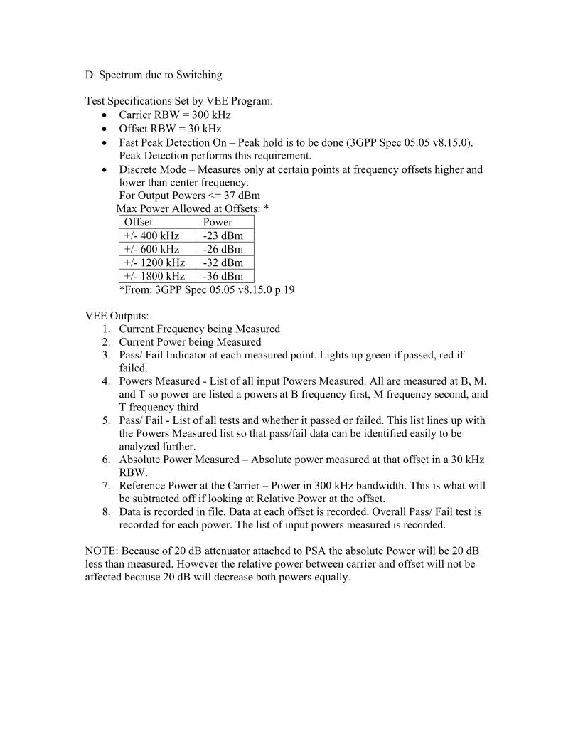
D. Spectrum due to Switching Test Specifications Set by VEE Program:
• Carrier RBW = 300 kHz • Offset RBW = 30 kHz • Fast Peak Detection On – Peak hold is to be done (3GPP Spec 05.05 v8.15.0).
Peak Detection performs this requirement. • Discrete Mode – Measures only at certain points at frequency offsets higher and
lower than center frequency. For Output Powers <= 37 dBm
Max Power Allowed at Offsets: * Offset Power +/- 400 kHz -23 dBm +/- 600 kHz -26 dBm +/- 1200 kHz -32 dBm +/- 1800 kHz -36 dBm
*From: 3GPP Spec 05.05 v8.15.0 p 19
VEE Outputs: 1. Current Frequency being Measured 2. Current Power being Measured 3. Pass/ Fail Indicator at each measured point. Lights up green if passed, red if
failed. 4. Powers Measured - List of all input Powers Measured. All are measured at B, M,
and T so power are listed a powers at B frequency first, M frequency second, and T frequency third.
5. Pass/ Fail - List of all tests and whether it passed or failed. This list lines up with the Powers Measured list so that pass/fail data can be identified easily to be analyzed further.
6. Absolute Power Measured – Absolute power measured at that offset in a 30 kHz RBW.
7. Reference Power at the Carrier – Power in 300 kHz bandwidth. This is what will be subtracted off if looking at Relative Power at the offset.
8. Data is recorded in file. Data at each offset is recorded. Overall Pass/ Fail test is recorded for each power. The list of input powers measured is recorded.
NOTE: Because of 20 dB attenuator attached to PSA the absolute Power will be 20 dB less than measured. However the relative power between carrier and offset will not be affected because 20 dB will decrease both powers equally.

V. Results for VSA Measurements
• Tests Performed: 1. Power versus Time (PvT) 2. Error Vector Magnitude (EVM)
Output RF Spectrum (ORFS) 3. Spectrum due to Modulation 4. Spectrum due to Switching
• PAs measured: RF3140 and ADL5551 • Pin swept from -20 dBm to 5 dBm. • Frequency Band P-GSM (890.2 MHz to 914.8 MHz) • B, M, T on data signifies Bottom (890.2 MHz), Middle (902.6 MHz), and Top
(914.8 MHz) Frequency of the P-GSM band respectively. • Averaged over 100 bursts. NOTE: 3GPP Spec says for ORFS to average over 200 bursts, but the measurement time is extensive and 100 bursts create a good enough average.
Results comments: Following are sample results from the measured tests for the RF3140 PA and one comparison of the RF3140 and ADL5551. Because the dynamic range proved to be a major issue for the VSA extensive results are not presented here for brevity.

A. Power Added Efficiency Results From respective specification sheet for each PA. (GSM900 refers to the frequency band which includes P-GSM band.)
RF3140 at Pout = 35 dBm 58% GSM900 ADL5551 at Pout = 32.5 dBm 55% GSM900 RF3133 at Pout = 35 dBm 53% GSM900
Results are using CW signal input, constant DC input, and averaged over three trials.
Figure 27. Output RF Power versus Input RF Power for all three PAs.
Figure 28. Power Added Efficiency versus Input RF Power for all three PAs.
RF3140 - PAE (%)PAE =
62.6366 Pin = -1
010203040506070
-20 -10 0
Input Power (dBm)
PAE
(%)
B
M
T
RF3133 - PAE (%)PAE =
54.7412Pin = -1
0
10
20
30
40
50
60
-20 -10 0Input Power (dBm)
PAE
(%)
B
M
T
ADL5551 - PAE (%)PAE =
53.2686Pin = -1
0
10
20
30
40
50
60
70
-20 -10 0Input Power (dBm)
PAE
(%)
B
M
T
RF3140 - Pout vs Pin (CW Signal)
Pout = 33.7486 Pin = -1
15
20
25
30
35
40
-20 -10 0Input Power (dBm)
Out
put P
ower
(dB
m)
B
M
T
RF3133 - Pout vs Pin (CW Signal)
Pout = 32.9002 Pin = -1
15
20
25
30
35
40
-20 -10 0Input Power (dBm)
Out
put P
ower
(dB
m)
B
M
T
ADL5551-Pout vs Pin (CW Signal)
Pout = 34.642 Pin = -1
15
20
25
30
35
40
-20 -10 0Input Power (dBm)
Out
put P
ower
(dB
m)
B
M
T

B. Power versus Time • Pass indicated by being inside upper and lower masks.
Figure 29. PvT Pin = -20 dBm Figure 30. PvT Pin = 3 dBm Figure 31. Zoomed in of Figure 29 Figure 32. Zoomed in of Figure 30 showing no signal inside mask. showing signal outside mask.

C. EVM Measurements
• Pass Indicated by:
EDGE Specs for Mobile Unit33: EVM RMS < 9.0% Peak EVM < 30% 95th Percentile <=15%
Pin = -20 dBm Pin = 0 dBm Pin = 3 dBm Figure 33. EVM measurement showing output for three input powers.

Power Amplifier Comparison – EVM Results RF3140 Figure 34. EVM results for RF3140 at a Pin = 3 dBm Pout = 35 dBm ADL5551 Figure 35. EVM results for ADL5551 at a Pin = 5 dBm Pout = 34.5 dBm

D. ORFS - Spectrum due to Modulation
• Pass Indicated by: EDGE Specs: At 35 dBm Pout 34 +/- 400 kHz < -60 dBc +/- 600 kHz < -62 dBc
Pin = -20 dBm Pin =3 dBm Figure 36. Spectrum due to Modulation measurement that shows output for two different input powers.
Pin = -20 dBm Pin = 3 dBm -400 kHz < 50 dBc -31.22 dBc +400 kHz < 50 dBc -31.74 dBc -600 kHz < 50 dBc -41.8 dBc +600 kHz < 50 dBc -42.08 dBc
Table 6. Summarized results from the data shown in Figure 36.

E. ORFS - Spectrum due to Switching
• Pass indicated by EDGE Specs: Pout = 35 Pout for < 37 dBm Pout35
+/- 400 kHz < -23 dBm +/- 600 kHz < -26 dBm
Pin = -20 dBm Pin = 3 dBm Figure 37. Spectrum due to Switching measurement that shows output for two different input powers.
Pin = -20 dBm Pin = 3 dBm -400 kHz -26.81 dBm 4.907 dBm +400 kHz -28.15 dBm 4.519 dBm -600 kHz -27.18 dBm -7.341 dBm +600 kHz -26.9 dBm -5.528 dBm
Table 7. Summarized results from the data shown in Figure 37.

G. Results of VSA Showing Dynamic Range as an Issue: The following show results of EDGE testing using the Electronic Signal
Generator (ESG) and the VSA with no PA.
Figure 38. Spectrum due to Modulation showing dynamic range issue.
Figure 39. Spectrum due to Switching showing dynamic range issue. Note: The first point in trace is not actually that high. Because signal is so low at this offset the triggering of the VSA has difficulty detecting the signal that low due to the dynamic range of the VSA. Therefore an incorrect reading is acquired at these high offsets. Observation: Can’t do offsets > 400 kHz due to dynamic range of VSA

VI. Results for PSA Measurements
• Tests Performed: 1. Power versus Time (PvT) 2. Error Vector Magnitude (EVM)
Output RF Spectrum (ORFS) 3. Spectrum due to Modulation 4. Spectrum due to Switching
• PAs measured: RF3140, RF3133, and ADL5551 • Pin swept from -20 dBm to 5 dBm. • Frequency Band P-GSM (890.2 MHz to 914.8 MHz) • B, M, T on data signifies Bottom (890.2 MHz), Middle (902.6 MHz), and Top
(914.8 MHz) Frequency of the P-GSM band respectively. • Averaged over 20 bursts.
NOTE: 3GPP Spec says for ORFS to average over 200 bursts, but the measurement time is extensive and 20 bursts create a good enough average.
Results Comments: Biasing 1 refers to the sharp transition biasing that lasts approx. 600 us. Biasing 2 refers to the smoother transition biasing that lasts approx. 600 us. Biasing 3 refers to the “starts early” smoother transition biasing that lasts approx. 800 us.

A. Power versus Time Results Shows Passes and Fails of the Power versus time test averaged over 20 bursts. Results then averaged over three trials. A Pass is a 0 and a Fail is a 1.
Figure 40. Power versus Time Data for 1 timeslot Biasing 3 for all three PAs.
R F 3 1 4 0 - P vT Ave ra g e d O ve ra ll P a s s / F a il
0
0 .2
0 .4
0 .6
0 .8
1
1 .2
-20 -18 -16 -14 -12 -10 -8 -6 -4 -2 0 2 4
In p u t P o w e r (d B m )
Pass
/ Fai
l - T
hree
Tria
ls
B M T
A D L 5 5 5 1 - P v T A v e ra g e d O v e ra ll P a s s / F a il
0
0 .2
0 .4
0 .6
0 .8
1
1 .2
-20 -18 -16 -14 -12 -10 -8 -6 -4 -2 0 2 4
In p u t P o w e r (d B m )
Pass
/ Fai
l - T
hree
Tria
ls
B M T
R F 3 1 3 3 - P v T A v e r a g e d O v e r a l l P a s s / F a i l
0
0 .2
0 .4
0 .6
0 .8
1
1 .2
-20 -18 -16 -14 -12 -10 -8 -6 -4 -2 0 2 4
In p u t P o w e r ( d B m )
Pass
/ Fai
l - T
hree
Tria
ls
B M T

B. EVM Measurements Shows EVM measurements for each PA. Three trials, each with 20 bursts, are averaged. The Bottom, Middle, and Top frequency data is overlaid and the pass/ fail line is displayed. Below the pass line the PA passes.
Figure 41. EVM Data for 1 timeslot Biasing 3 for all three PAs.

C. ORFS - Spectrum due to Modulation
As stated in the description of the measurements taken, the B, M, and T frequencies and the upper and lower offsets were all measured. After analysis of the data is would found that the B, M, and T data followed each other closely as well as the upper and lower offsets as shown Figure 42. Therefore in the further analysis the results of only one frequency and only at the lower offset were shown here.
Figure 43 shows the results of Spectrum due to Modulation for the three power amplifiers.
Figure 44 through Figure 46 shows the results of Spectrum due to Modulation for the RF3133 showing the differences between the Biasing 1, Biasing 3, and constant DC biasing.
RF3133 - ORFS - Spectrum due to Modulation - Biasing 3
-90
-80
-70
-60
-50
-40
-30
-20
-10
0-20 -15 -10 -5 0 5
Pin (dBm)
Rel
ativ
e Po
wer
(dB
c)
-200 (B) -200 (M) -200 (T) +200 (B) +200 (M) +200 (T) -250 (B) -250 (M) -250 (T) +250 (B) +250 (M) +250 (T) -400 (B) -400 (M) -400 (T) +400 (B) +400 (M) +400 (T) -600 (B) -600 (M) -600 (T) +600 (B) +600 (M) +600 (T) -1200 (B) -1200 (M) -1200 (T) +1200 (B) +1200 (M) +1200 (T) -1800 (B) -1800 (M) -1800 (T) +1800 (B) +1800 (M) +1800 (T)
Figure 42. Spectrum due to Modulation – RF3133 using Biasing 3

RF3140 - ORFS - Spectrum due to Modulation - Baising 3
-90
-80
-70
-60
-50
-40
-30
-20
-10
0-20 -15 -10 -5 0 5
Pin (dBm)
Rel
ativ
e Po
wer
(dB
c) -200 (B)
-250 (B)
-400 (B)
-600 (B)
-1200 (B)
-1800 (B)
Pass 200 kHz
Pass 250 kHz
Pass 400 kHz
Pass 600 kHz
Pass 1200 kHz
Pass 1800 kHz
ADL5551 - ORFS - Spectrum due to Modulation-Baising 3
-90
-80
-70
-60
-50
-40
-30
-20
-10
0-20 -15 -10 -5 0 5
Pin (dBm)
Rel
ativ
e Po
wer
(dB
c)
-200 (B)
-250 (B)
-400 (B)
-600 (B)
-1200 (B)
-1800 (B)
Pass 200 kHz
Pass 250 kHz
Pass 400 kHz
Pass 600 kHz
Pass 1200 kHz
Pass 1800 kHz
RF3133 - ORFS - Spectrum due to Modulation - Baising 3
-90
-80
-70
-60
-50
-40
-30
-20
-10
0-20 -15 -10 -5 0 5
Pin (dBm)
Rel
ativ
e Po
wer
(dB
c)
-200 (B)
-250 (B)
-400 (B)
-600 (B)
-1200 (B)
-1800 (B)
Pass 200 kHz
Pass 250 kHz
Pass 400 kHz
Pass 600 kHz
Pass 1200 kHz
Pass 1800 kHz
Figure 43. Spectrum due to Modulation – all PAs using Biasing 3

ORFS - Spectrum due to Modulation
-90
-80
-70
-60
-50
-40
-30
-20
-10
0-25 -20 -15 -10 -5 0 5 10
Pin (dBm)
Rel
ativ
e Po
wer
(dB
c) -200 (B)
-250 (B)
-400 (B)
-600 (B)
-1200 (B)
-1800 (B)
Pass 200 kHz
Pass 250 kHz
Pass 400 kHz
Pass 600 kHz
Pass 1200 kHz
Pass 1800 kHz
Figure 44. RF3133- DC Biasing 1 – sharp transitions
ORFS - Spectrum due to Modulation
-90
-80
-70
-60
-50
-40
-30
-20
-10
0-25 -20 -15 -10 -5 0 5 10
Pin (dBm)
Rel
ativ
e Po
wer
(dB
c)
-200 (B)
-250 (B)
-400 (B)
-600 (B)
-1200 (B)
-1800 (B)
Pass 200 kHz
Pass 250 kHz
Pass 400 kHz
Pass 600 kHz
Pass 1200 kHz
Pass 1800 kHz
Figure 45. RF3133- DC Biasing 3 – smooth transitions and starts early
ORFS - Spectrum due to Modulation
-90
-80
-70
-60
-50
-40
-30
-20
-10
0-25 -20 -15 -10 -5 0 5 10
Pin (dBm)
Rel
ativ
e Po
wer
(dB
c)
-200 (B)
-250 (B)
-400 (B)
-600 (B)
-1200 (B)
-1800 (B)
Pass 200 kHz
Pass 250 kHz
Pass 400 kHz
Pass 600 kHz
Pass 1200 kHz
Pass 1800 kHz
Figure 46. RF3133- DC biasing constant - No burst biasing

D. ORFS - Spectrum due to Switching
Figure 47 shows the results of Spectrum due to Switching for the three PAs. Arrow points to first failure and tells what input power it occurred on. Figure 48 through Figure 50 shows the results of Spectrum due to Modulation for the RF3133 showing the differences between the Biasing 1, Biasing 3, and constant DC biasing.
Figure 47. Spectrum due to Switching Biasing 3 for all three PAs.
RF3133- ORFS - Spectrum due to Switching
-13 dBm
-70-60-50-40-30-20-10
01020
-20 -15 -10 -5 0 5
Pin (dBm)
Abs
olut
e Po
wer
(dB
m)
-400 (B)
-600 (B)
-1200 (B)
-1800 (B)
Pass 400 kHz
Pass 600 kHz
Pass 1200 kHz
Pass 1800 kHz
RF3140 - ORFS - Spectrum due to Switching
-11 dBm
-70-60-50-40-30-20-10
01020
-20 -15 -10 -5 0 5
Pin (dBm)
Abs
olut
e Po
wer
(dB
m)
-400 (B)
-600 (B)
-1200 (B)
-1800 (B)
Pass 400 kHz
Pass 600 kHz
Pass 1200 kHz
Pass 1800 kHz
ADL5551 - ORFS - Spectrum due to Switching
-14 dBm
-60
-50
-40
-30
-20
-10
0
10
20
-20 -15 -10 -5 0 5
Pin (dBm)
Abs
olut
e Po
wer
(dB
m)
-400 (B)
-600 (B)
-1200 (B)
-1800 (B)
Pass 400 kHz
Pass 600 kHz
Pass 1200kHz

RF3133- ORFS - Spectrum due to Switching
All Fail
-40-35-30-25-20-15-10-505
1015
-20 -15 -10 -5 0 5
Pin (dBm)
Abs
olut
e Po
wer
(dB
m)
-400 (B)
-600 (B)
-1200 (B)
-1800 (B)
Pass 400 kHz
Pass 600 kHz
Pass 1200 kHz
Pass 1800 kHz
Figure 48. RF3133- DC Biasing 1 – sharp transitions
RF3133- ORFS - Spectrum due to Switching
-13 dBm
-70-60-50-40-30-20-10
01020
-20 -15 -10 -5 0 5
Pin (dBm)
Abs
olut
e Po
wer
(dB
m)
-400 (B)
-600 (B)
-1200 (B)
-1800 (B)
Pass 400 kHz
Pass 600 kHz
Pass 1200 kHz
Pass 1800 kHz
Figure 49. RF3133- DC Biasing 3 – smooth transitions and starts early
RF3133- ORFS - Spectrum due to Switching
-8 dBm
-70
-60
-50
-40
-30
-20
-10
0
10
-20 -15 -10 -5 0 5
Pin (dBm)
Abs
olut
e Po
wer
(dB
m)
-400 (B)
-600 (B)
-1200 (B)
-1800 (B)
Pass 400 kHz
Pass 600 kHz
Pass 1200 kHz
Pass 1800 kHz
Figure 50. RF3133- DC biasing constant - No burst biasing

VII. Conclusions VSA measurements -
VSA does not have enough dynamic range to be able to measure offsets greater than 600kHz from center frequency therefore PSA must be used. As can be seen from below measured data the VSA cannot measure signal below –50 dBc (dB below carrier power).
Measured from VSA Measured from PSA Bias Bursting
The DC biasing waveform that has a smoother transition and starts earlier shows better results in the RF output as shown in the spectrum due to switching transients’ results. Out of all the bias bursting measurements, the spectrum due to modulation results has little difference. When not turning on and off the bias with the RF burst, the spectrum due to modulation and spectrum due to switching both show much improved results. Therefore there is a tradeoff between allowing the DC bursting to be on for a constant amount of time and have less adjacent channel power present, or do the biasing to simulate better battery performance but allow adjacent channel power. EVM The RF3133 well outperformed the other two power amplifiers. The error starts to grow but then takes a dip in the RF3133 thus making much higher input levels pass compared to the RF3140 and ADL5551. EVM tests were better for the RF3133 but still did not pass for input powers greater then –7 dBm, which is not acceptable for use in an actual EDGE cellular phone. PvT The distortions in the time domain had little effect on all the tested power amplifiers. At high powers of greater than –2 dBm the signal did distort and go outside the mask and thus fail, but this is a high input power compared to the failures in the other tests.

ORFS – Spectrum due to Modulation All tests between the power amplifiers were similar for this test. The problem offset was found to be the +/- 400 kHz offset and was shown to cause the PA to fail at a lower input power than any other offset. ORFS – Spectrum due to Switching When doing any sort of bias bursting, this test proved to be the worst and the power amplifiers failed at a low input power level. As was stated above the spectrum to switching power could be diminished by using a different waveform structure for the DC biasing so therefore potentially another improved waveform could be developed to provide even less spectrum due to switching power. Two Time Slots The differences are very small in the data between having one and having two consecutive timeslots active for input power. For EVM, Power versus Time, and Spectrum due to Modulation the data is practically identical. For Spectrum due to Switching the data does show that it is worse for all PAs when two time slots are active. This is as to be expected because more transients exist in the signal due to two bursts existing.
Overall all measured PAs do not have low enough distortion at high powers to meet EDGE specifications. When designing an EDGE mobile telephone there are many design constraints. To make EDGE a reality, inexpensive power amplifiers that have a large linear range need to be developed. The development of the power amplifiers themselves is only as good as the measurement procedures that can accurately characterize power amplifiers. As these and other measurement procedures are investigated the design of the power amplifiers can be improved to accommodate these constraints.

VIII. References