Embed Size (px)
Citation preview
ARTICLE IN PRESS
0022-0248/$ - se
doi:10.1016/j.jc
�CorrespondE-mail addr
Journal of Crystal Growth 294 (2006) 427–431
www.elsevier.com/locate/jcrysgro
Growth of transparent conducting nanocrystalline Al doped ZnO thinfilms by pulsed laser deposition
R.K. Shukla�, Anchal Srivastava, Atul Srivastava, K.C. Dubey
Department of Physics, Lucknow University, 22, Milini Park, Lucknow University Campus, Lucknow 226007, India
Received 31 May 2006; accepted 19 June 2006
Communicated by R. Kern
Available online 14 August 2006
Abstract
Nanocrystalline thin films of Al doped ZnO (Al:0–5 at%) with low electrical resistivity and high optical transparency have been grown
by pulsed laser deposition. X-ray diffraction patterns showed the presence of hexagonal wurtzite ZnO phase with strong c-axis
orientation in all the cases. The c-axis lattice parameter was found to increase with increase in Al doping. The average grain size in the
film decreases from �38 to �25 nm with increasing Al concentration from 0 to 5 at%. For a critical doping of 2 at%, the resistivity of the
AZO film is minimum (6� 10�4O-cm) and the average optical transparency is nearly 85%. The band gap increases with increase in
doping which is in accordance to Burstein–Moss shift. A blue shift in the absorption edge of ZnO with increasing Al concentration in the
film is noteworthy as it leads to increase in the width of the transmission window.
r 2006 Published by Elsevier B.V.
PACS: 61.66.Dk; 78.66.Bz; 84.70.+p
Keywords: A1. Nanocrystalline; A1. Optical transparency; A1. Transmission window; A3. Pulsed laser deposition; Bl. Al doped ZnO films; B2. Low
electrical resistivity
1. Introduction
Currently there is a world wide interest in developingtransparent conducting oxides and transparent oxide semi-conductors for the development of transparent electronicsand photonic devices and transparent conducting electrodes(TCE) for solar cells [1], flat panel display [2], organic lightemitting devices [3–5], surface acoustic wave device [6],piezoelectric transducers [7] and gas sensing devices. Thewidely explored transparent oxide semiconductors are In2O3
and SnO2, etc. or combination of In2O3 and SnO2 such asindium tin oxide (ITO). Indium, the main constituent of ITOis a toxic material besides being expensive and scarce,whereas ZnO is a non-toxic, inexpensive and abundantmaterial [4] and also it is chemically and thermally stable.Zinc oxide, a II–VI compound is transparent semiconductor
e front matter r 2006 Published by Elsevier B.V.
rysgro.2006.06.035
ing author. Tel.: +910522 2740449.
ess: [email protected] (R.K. Shukla).
with naturally occurring n-type conductivity and is emergingas an alternative potential material to ITO for thin filmtransparent electrode applications. The notable properties ofZnO are its direct band gap of 3.27 eV at room temperatureand its high exciton binding energy of �60meV, which ismore than some widely used wide band gap material, such asZnSe (20meV) [6] and GaN (25meV) [8].Group III metal dopants, such as Al, In and Ga have
been suitably added to increase the electrical conductivityand transparency of ZnO films. The undoped ZnO grownon NaCl at substrate temperature of �300 1C demon-strated significant epitaxial growth, suggesting that this isthe suitable minimum temperature for growth of highquality ZnO film by pulsed laser deposition (PLD) [9]. Inthis paper, we report our studies on ZnO and Al dopedZnO films grown by PLD on heated glass substrate at400 1C. PLD has been shown to yield high quality c-axisoriented ZnO films at lower substrate temperature com-pared to many other techniques [10,11].
ARTICLE IN PRESSR.K. Shukla et al. / Journal of Crystal Growth 294 (2006) 427–431428
2. Experiments
The ZnO (99.999% purity) and Al2O3 (99.997% purity)were obtained from Aldrich chemical company, Inc. Theceramic pellets of undoped and Al doped zinc oxide (AZO)are prepared using conventional cold ceramic pressingtechnique. The AZO pellets with 2, 3 and 5 at% of Al areprepared. The sintered targets are polished before loadingin the PLD chamber to minimize the problem ofparticulates arising due to rough and irregular surfacemorphology of target surface. Float glass is used assubstrate, which was cleaned using methanol and deionizedwater. ZnO and AZO pellets were ablated by thirdharmonic of Q-Switched Nd:YAG laser (Quantel YG980,
20 30 40 50 60 70 80
ZnO
2θ
2%Al:ZnO
Inte
nsity
(ar
b.un
it)
3%Al:ZnO
(000
2) Z
nO
(000
4) Z
nO
5%Al:ZnO
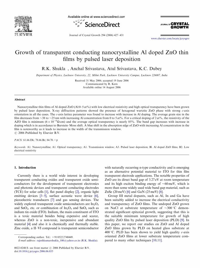
Fig. 1. The y–2y XRD patterns of ZnO and AZO thin films deposited at
400 1C.
Table 1
Variation of structural parameters of ZnO and AZO thin films
Material 2y FWHM Interplanar spacing (nm)
ZnO 34.451 0.2161 0.26015
2 at%Al:ZnO 34.391 0.2221 0.26056
3 at%Al:ZnO 34.221 0.2451 0.26181
5 at%Al:ZnO 34.201 0.3281 0.26196
355 nm, 10Hz and 6 ns pulse duration) with a fluence of2 J/cm2. The distance between the substrate and target iskept fixed at 6 cm. The average thickness of the film is�250 nm. The substrate temperature is maintained at400 1C and the oxygen partial pressure is kept at�10�3 Torr. The films deposited by PLD in vacuum aretypically Zn-rich due to recondensation of Zn onto thesurface of the target [12]. Therefore ZnO films are typicallygrown in the background pressure of oxygen [13].The X-ray diffraction of the samples has been obtained
using a fully automatic high resolution XRD system(Rigaku, Japan). The wavelength used is Cu-Ka1, i.e.1.540568 A. The transmittance of the thin film is measuredby an UV–VIS-NIR dual beam spectrophotometer (Shi-madzu model UV 3101 PC) in the wavelength range200–900 nm. The sheet resistance (Rsh) measurements weremade using a four-point probe. Assuming the thickness ofthe film to be uniform, the film resistivities have beendetermined by taking the product of Rsh and film thickness.Hall mobility and carrier density measurements were madeusing the Vander Pauw method at room temperature withfield strength of 4 kG.
3. Results and discussion
3.1. Structural properties
The y–2y XRD patterns of ZnO and AZO thin filmsdeposited at 400 1C are shown in Fig. 1. The ZnO relatedreflections (2y�341) in each pattern are obtained in (0 0 0 2)plane indicating a strong c-axis orientation with hexagonalwurtzite structure. For pure ZnO the peak occurs at 34.451,for 2, 3 and 5 at% doping in ZnO the XRD peaks occur at34.391, 34.221 and 34.201, respectively. XRD peak shifts tolower values of y with increasing Al concentration in AZOfilms. This results in an increase in the lattice parameter inc-direction and also in the interplanar spacing d as it isequal to c/2 for (0 0 0 2) plane in hexagonal wurtzitestructure. The c-lattice constant calculated from the XRDpatterns of ZnO and AZO films is in the range between0.52030 and 0.52392 nm (Table 1), which are larger thanJCPDS value 0.51948 nm for ZnO powder. This increase inlattice parameter of the AZO films probably occurs byincorporation of Al+3 ions in the interstitial position [14].Substitutional incorporation of Al ion into Zn2+ sites isnot occurring in the present conditions of growth. As theradius (0.53 A) of Al3+ ions is smaller than that (0.72 A) of
Grain size (nm) Strain c-lattice constant (nm)
38.5 1.568� 10�3 0.52030
37.5 1.333� 10�3 0.52112
33.9 1.546� 10�3 0.52363
25.4 2.048� 10�3 0.52392
ARTICLE IN PRESSR.K. Shukla et al. / Journal of Crystal Growth 294 (2006) 427–431 429
Zn2+, the substitution of Al3+ for Zn2+ is not expected toresult in lattice expansion. The increase in c-axis latticeparameter may also be a result of strain effect due tothermal expansion coefficient mismatch between the film(7� 10�6 /1C) [15], and glass substrate (4.6� 10�6 /1C).AZO films reported in Ref. [5] also have increased c-valueswhereas those reported in Ref. [9] have decreased c-values.Increase in the interplanar spacing leads to decrease in thefilm density and the refractive index of the film. Also Aldoping affects the crystalline quality of the films as itchanges the intensity, as well as full-width at half-maximaof the XRD peaks. The intensity decreases and the linewidth increases monotonically with increase in the percen-tage of Al doping Fig. 1. It indicates that there is a loweringin crystalline nature/ c-axis orientation and reduction in thegrain size of the films. The grain size is calculated usingDebye-Scherer formula, which decreases from �38 to�25 nm from 0 to 5 at% (Table 1).
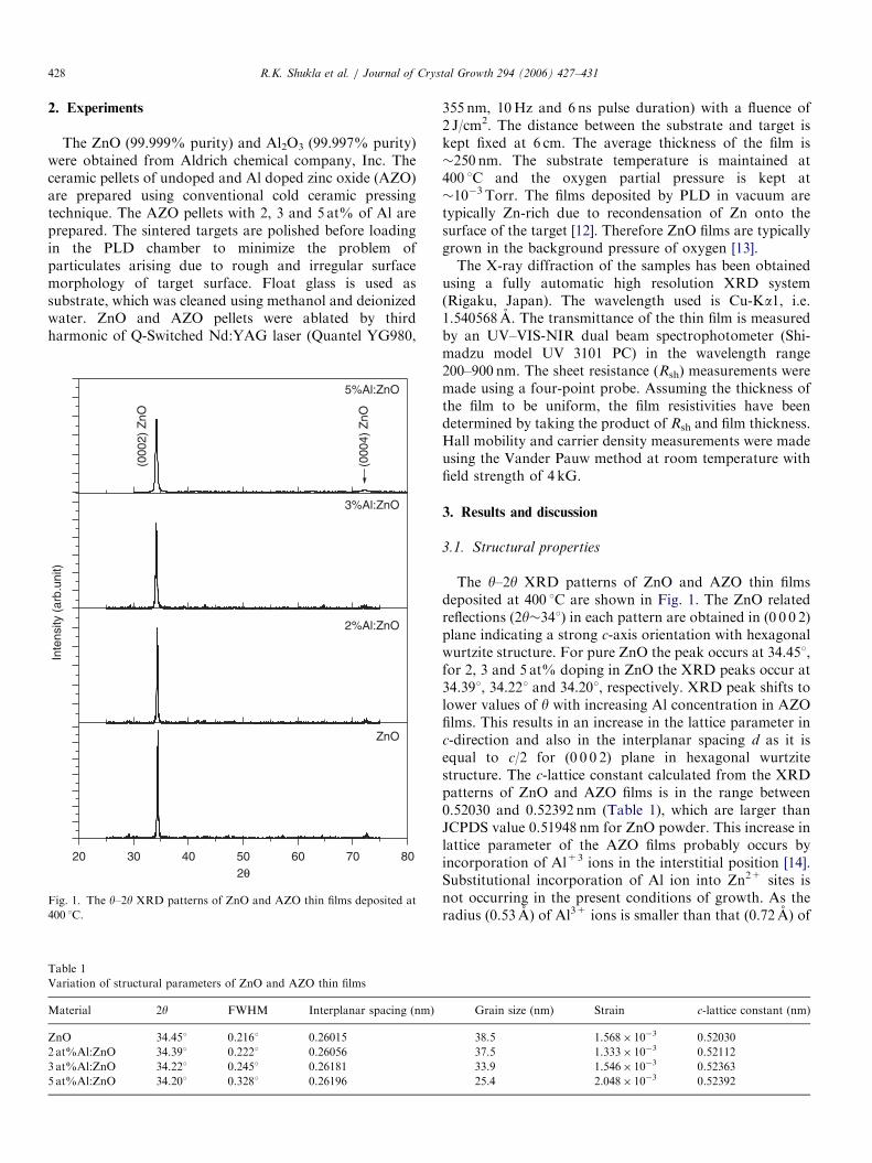
The morphology of the films has been studied usingscanning electron micrographs. Fig. 2 shows a uniformgrowth throughout the substrate.
Fig. 2. Scanning electron micrograph of pure ZnO film (a) and 2 at% Al
doped ZnO film (b).
3.2. Optical properties
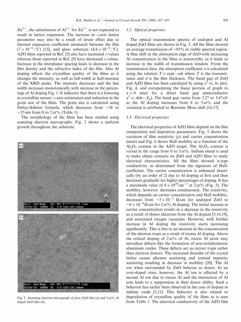
The optical transmission spectra of undoped and Aldoped ZnO films are shown in Fig. 3. All the films showedan average transmission of �85% in visible spectral region.A blue shift in the absorption edge of ZnO with increasingAl concentration in the films is noteworthy as it leads toincrease in the width of transmission window. From thetransmission data, the absorption coefficient a is calculatedusing the relation T ¼ exp(�ad) where T is the transmit-tance and d is the film thickness. The band gap of ZnOand AZO films has been calculated by using a2 vs. hu plot,Fig. 4, and extrapolating the linear portion of graph toa ¼ 0 since for a direct band gap semiconductora2 ¼ A(hu�Eg). The band gap varies from 3.27 to 3.67 eVas the Al doping increases from 0 to 5 at% and thevariation is attributed to Burstein–Moss shift [16,17].
3.3. Electrical properties
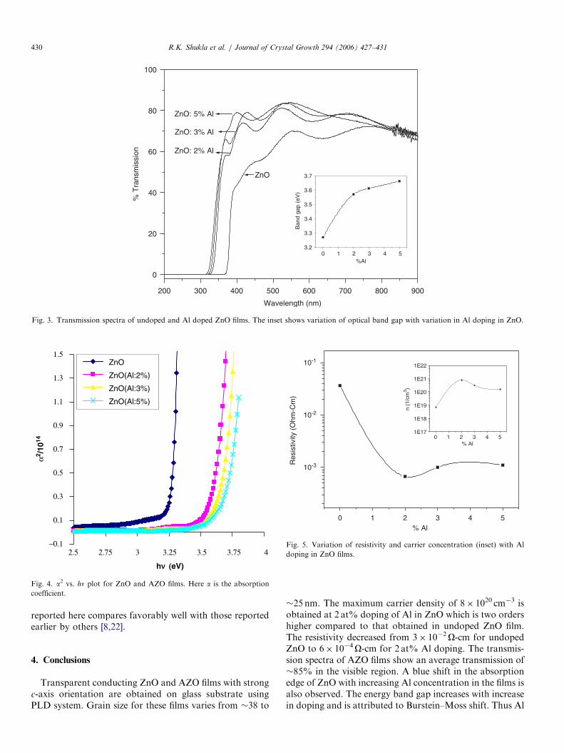
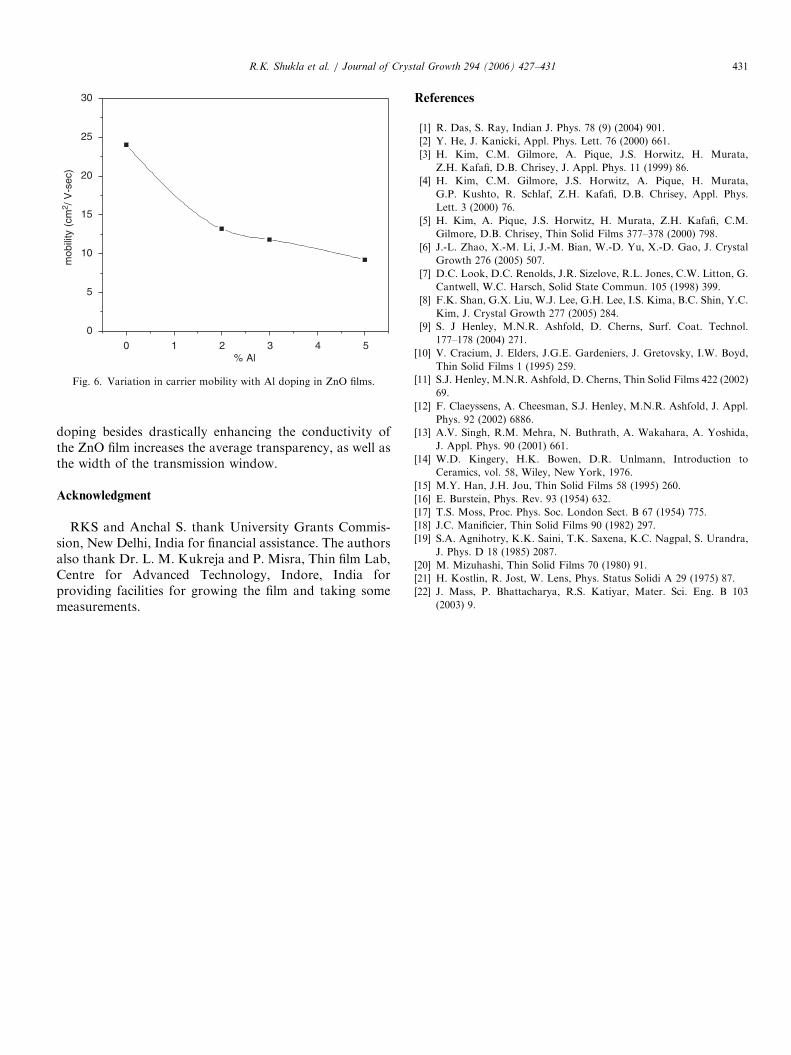
The electrical properties of AZO films depend on the filmcomposition and deposition parameters. Fig. 5 shows thevariation of film resistivity (r) and carrier concentration(inset) and Fig. 6 shows Hall mobility as a function of theAl2O3 content in the AZO target. The Al2O3 content isvaried in the range from 0 to 5 at%. Indium metal is usedto make ohmic contacts on ZnO and AZO films to studyelectrical characteristics. All the films showed n-typeconductivity as determined from the signature of Hall-coefficient. The carrier concentration is enhanced drasti-cally (by an order of 2) due to Al doping at first and thendecreases gradually for higher percentages of doping. It hasa maximum value of 8� 1020 cm�3 at 2 at% (Fig. 5). Themobility, however, decreases continuously. The resistivity,which depends on carrier concentration and Hall mobility,decreases from �3� 10�2 O-cm for undoped ZnO to�6� 10�4O-cm for 2 at% Al doping. The initial increase incarrier concentration results in a decrease in the resistivityas a result of donor electrons from the Al dopant [3,18,19],and associated oxygen vacancies. However, with furtherincrease in Al doping the resistivity starts increasingsignificantly. This is due to an increase in the concentrationof the electron traps as a result of excess Al doping. Abovethe critical doping of 2 at% of Al, excess Al atom mayintroduce defects like the formation of non-stoichiometricaluminum oxides. These defects act as carrier traps ratherthan electron donors. The increased disorder of the crystallattice causes phonon scattering and ionized impurityscattering resulting in decrease in mobility [20]. The Alion when surrounded by ZnO behaves as donor. In anover-doped state, however, the Al ion is affected by asecond Al ion due to excess Al and the interaction of Alions leads to a suppression in their donor ability. Such abehavior has earlier been observed in the case of dopant inindium oxide [3,21]. This behavior is also related todegradation of crystalline quality of the films as is seenfrom Table 1. The electrical conductivity of the AZO film
ARTICLE IN PRESS
−0.1
0.1
0.3
0.5
0.7
0.9
1.1
1.3
1.5
2.5 2.75 3 3.25 3.5 3.75 4
hν (ν (eV)
α2/101
4
ZnO
ZnO(Al:2%)
ZnO(Al:3%)
ZnO(Al:5%)
Fig. 4. a2 vs. hn plot for ZnO and AZO films. Here a is the absorption
coefficient.
200 300 400 500 600 700 800 900
0
20
40
60
80
100
3.20 1 2 3 4 5
3.3
3.4
3.5
3.6
3.7
Ban
d ga
p (e
V)
%Al
ZnO: 5% Al
ZnO: 3% Al
ZnO: 2% Al
ZnO
% T
rans
mis
sion
Wavelength (nm)
Fig. 3. Transmission spectra of undoped and Al doped ZnO films. The inset shows variation of optical band gap with variation in Al doping in ZnO.
0 5
10-3
10-2
10-1
0 1 2 3 4 51E17
1E18
1E19
1E20
1E21
1E22
n (1
/cm
3 )
% Al
Res
istiv
ity (
Ohm
-Cm
)
% Al1 2 3 4
Fig. 5. Variation of resistivity and carrier concentration (inset) with Al
doping in ZnO films.
R.K. Shukla et al. / Journal of Crystal Growth 294 (2006) 427–431430
reported here compares favorably well with those reportedearlier by others [8,22].
4. Conclusions
Transparent conducting ZnO and AZO films with strongc-axis orientation are obtained on glass substrate usingPLD system. Grain size for these films varies from �38 to
�25 nm. The maximum carrier density of 8� 1020 cm�3 isobtained at 2 at% doping of Al in ZnO which is two ordershigher compared to that obtained in undoped ZnO film.The resistivity decreased from 3� 10�2O-cm for undopedZnO to 6� 10�4O-cm for 2 at% Al doping. The transmis-sion spectra of AZO films show an average transmission of�85% in the visible region. A blue shift in the absorptionedge of ZnO with increasing Al concentration in the films isalso observed. The energy band gap increases with increasein doping and is attributed to Burstein–Moss shift. Thus Al
ARTICLE IN PRESS
0 1 2 3 4 5
0
5
10
15
20
25
30
mob
ility
(cm
2 / V
-sec
)
% Al
Fig. 6. Variation in carrier mobility with Al doping in ZnO films.
R.K. Shukla et al. / Journal of Crystal Growth 294 (2006) 427–431 431
doping besides drastically enhancing the conductivity ofthe ZnO film increases the average transparency, as well asthe width of the transmission window.
Acknowledgment
RKS and Anchal S. thank University Grants Commis-sion, New Delhi, India for financial assistance. The authorsalso thank Dr. L. M. Kukreja and P. Misra, Thin film Lab,Centre for Advanced Technology, Indore, India forproviding facilities for growing the film and taking somemeasurements.
References
[1] R. Das, S. Ray, Indian J. Phys. 78 (9) (2004) 901.
[2] Y. He, J. Kanicki, Appl. Phys. Lett. 76 (2000) 661.
[3] H. Kim, C.M. Gilmore, A. Pique, J.S. Horwitz, H. Murata,
Z.H. Kafafi, D.B. Chrisey, J. Appl. Phys. 11 (1999) 86.
[4] H. Kim, C.M. Gilmore, J.S. Horwitz, A. Pique, H. Murata,
G.P. Kushto, R. Schlaf, Z.H. Kafafi, D.B. Chrisey, Appl. Phys.
Lett. 3 (2000) 76.
[5] H. Kim, A. Pique, J.S. Horwitz, H. Murata, Z.H. Kafafi, C.M.
Gilmore, D.B. Chrisey, Thin Solid Films 377–378 (2000) 798.
[6] J.-L. Zhao, X.-M. Li, J.-M. Bian, W.-D. Yu, X.-D. Gao, J. Crystal
Growth 276 (2005) 507.
[7] D.C. Look, D.C. Renolds, J.R. Sizelove, R.L. Jones, C.W. Litton, G.
Cantwell, W.C. Harsch, Solid State Commun. 105 (1998) 399.
[8] F.K. Shan, G.X. Liu, W.J. Lee, G.H. Lee, I.S. Kima, B.C. Shin, Y.C.
Kim, J. Crystal Growth 277 (2005) 284.
[9] S. J Henley, M.N.R. Ashfold, D. Cherns, Surf. Coat. Technol.
177–178 (2004) 271.
[10] V. Cracium, J. Elders, J.G.E. Gardeniers, J. Gretovsky, I.W. Boyd,
Thin Solid Films 1 (1995) 259.
[11] S.J. Henley, M.N.R. Ashfold, D. Cherns, Thin Solid Films 422 (2002)
69.
[12] F. Claeyssens, A. Cheesman, S.J. Henley, M.N.R. Ashfold, J. Appl.
Phys. 92 (2002) 6886.
[13] A.V. Singh, R.M. Mehra, N. Buthrath, A. Wakahara, A. Yoshida,
J. Appl. Phys. 90 (2001) 661.
[14] W.D. Kingery, H.K. Bowen, D.R. Unlmann, Introduction to
Ceramics, vol. 58, Wiley, New York, 1976.
[15] M.Y. Han, J.H. Jou, Thin Solid Films 58 (1995) 260.
[16] E. Burstein, Phys. Rev. 93 (1954) 632.
[17] T.S. Moss, Proc. Phys. Soc. London Sect. B 67 (1954) 775.
[18] J.C. Manificier, Thin Solid Films 90 (1982) 297.
[19] S.A. Agnihotry, K.K. Saini, T.K. Saxena, K.C. Nagpal, S. Urandra,
J. Phys. D 18 (1985) 2087.
[20] M. Mizuhashi, Thin Solid Films 70 (1980) 91.
[21] H. Kostlin, R. Jost, W. Lens, Phys. Status Solidi A 29 (1975) 87.
[22] J. Mass, P. Bhattacharya, R.S. Katiyar, Mater. Sci. Eng. B 103
(2003) 9.


![Optical and structural properties of Si-doped ZnO thin films...Si-doped ZnO nanocomposites [8–10] and nanorods [11]. In the present work we examine Si-doped ZnO thin films pro-](https://img.pdfslide.us/doc/110x75/610af404b2c50b3ec432d369/optical-and-structural-properties-of-si-doped-zno-thin-films-si-doped-zno-nanocomposites.jpg)