Embed Size (px)
Citation preview
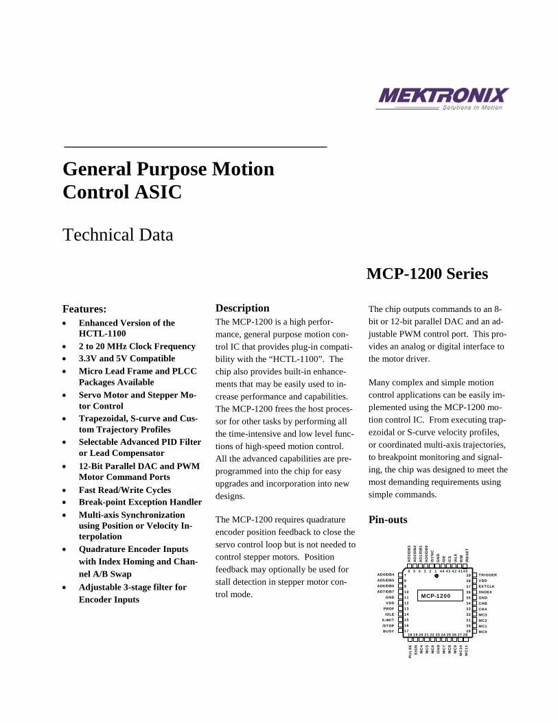
6 5 4 3 2 1 44 43 42 41 40 7 8 9 10 11 12 13 14 15 16 17
18 19 20 21 22 23 24 25 26 27 28
39 38 37 36 35 34 33 32 31 30 29
AD4/DB4 AD5/DB5 AD6/DB6 AD7/DB7
GND VDD
PROF IDLE
/LIMIT /STOP BUSY
MCP-1200
AD
3/D
B3
AD
2/D
B2
AD
1/D
B1
AD
0/D
B0
/SY
NC
G
ND
/O
E
/CS
/A
LE
R/W
/R
ES
ET
TRIGGER VDD EXTCLK /INDEX GND CHB CHA MC3 MC2 MC1 MC0
PU
LSE
S
IGN
M
C4
M
C5
M
C6
G
ND
M
C7
M
C8
M
C9
M
C10
M
C11
General Purpose Motion Control ASIC Technical Data MCP-1200 Series Features: • Enhanced Version of the
HCTL-1100 • 2 to 20 MHz Clock Frequency • 3.3V and 5V Compatible • Micro Lead Frame and PLCC
Packages Available • Servo Motor and Stepper Mo-
tor Control • Trapezoidal, S-curve and Cus-
tom Trajectory Profiles • Selectable Advanced PID Filter
or Lead Compensator • 12-Bit Parallel DAC and PWM
Motor Command Ports • Fast Read/Write Cycles • Break-point Exception Handler • Multi-axis Synchronization
using Position or Velocity In-terpolation
• Quadrature Encoder Inputs with Index Homing and Chan-nel A/B Swap
• Adjustable 3-stage filter for Encoder Inputs
Description The MCP-1200 is a high perfor-mance, general purpose motion con-trol IC that provides plug-in compati-bility with the “HCTL-1100”. The chip also provides built-in enhance-ments that may be easily used to in-crease performance and capabilities. The MCP-1200 frees the host proces-sor for other tasks by performing all the time-intensive and low level func-tions of high-speed motion control. All the advanced capabilities are pre-programmed into the chip for easy upgrades and incorporation into new designs. The MCP-1200 requires quadrature encoder position feedback to close the servo control loop but is not needed to control stepper motors. Position feedback may optionally be used for stall detection in stepper motor con-trol mode.
The chip outputs commands to an 8-bit or 12-bit parallel DAC and an ad-justable PWM control port. This pro-vides an analog or digital interface to the motor driver. Many complex and simple motion control applications can be easily im-plemented using the MCP-1200 mo-tion control IC. From executing trap-ezoidal or S-curve velocity profiles, or coordinated multi-axis trajectories, to breakpoint monitoring and signal-ing, the chip was designed to meet the most demanding requirements using simple commands. Pin-outs
2
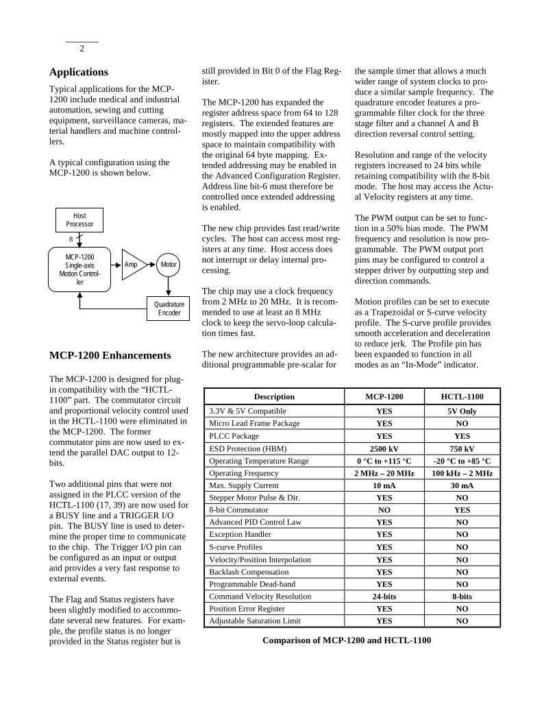
Applications Typical applications for the MCP-1200 include medical and industrial automation, sewing and cutting equipment, surveillance cameras, ma-terial handlers and machine control-lers. A typical configuration using the MCP-1200 is shown below.
MCP-1200 Enhancements The MCP-1200 is designed for plug-in compatibility with the “HCTL-1100” part. The commutator circuit and proportional velocity control used in the HCTL-1100 were eliminated in the MCP-1200. The former commutator pins are now used to ex-tend the parallel DAC output to 12-bits. Two additional pins that were not assigned in the PLCC version of the HCTL-1100 (17, 39) are now used for a BUSY line and a TRIGGER I/O pin. The BUSY line is used to deter-mine the proper time to communicate to the chip. The Trigger I/O pin can be configured as an input or output and provides a very fast response to external events. The Flag and Status registers have been slightly modified to accommo-date several new features. For exam-ple, the profile status is no longer provided in the Status register but is
still provided in Bit 0 of the Flag Reg-ister. The MCP-1200 has expanded the register address space from 64 to 128 registers. The extended features are mostly mapped into the upper address space to maintain compatibility with the original 64 byte mapping. Ex-tended addressing may be enabled in the Advanced Configuration Register. Address line bit-6 must therefore be controlled once extended addressing is enabled. The new chip provides fast read/write cycles. The host can access most reg-isters at any time. Host access does not interrupt or delay internal pro-cessing. The chip may use a clock frequency from 2 MHz to 20 MHz. It is recom-mended to use at least an 8 MHz clock to keep the servo-loop calcula-tion times fast. The new architecture provides an ad-ditional programmable pre-scalar for
the sample timer that allows a much wider range of system clocks to pro-duce a similar sample frequency. The quadrature encoder features a pro-grammable filter clock for the three stage filter and a channel A and B direction reversal control setting. Resolution and range of the velocity registers increased to 24 bits while retaining compatibility with the 8-bit mode. The host may access the Actu-al Velocity registers at any time. The PWM output can be set to func-tion in a 50% bias mode. The PWM frequency and resolution is now pro-grammable. The PWM output port pins may be configured to control a stepper driver by outputting step and direction commands. Motion profiles can be set to execute as a Trapezoidal or S-curve velocity profile. The S-curve profile provides smooth acceleration and deceleration to reduce jerk. The Profile pin has been expanded to function in all modes as an “In-Mode” indicator.
Description MCP-1200 HCTL-1100
3.3V & 5V Compatible YES 5V Only Micro Lead Frame Package YES NO PLCC Package YES YES ESD Protection (HBM) 2500 kV 750 kV Operating Temperature Range 0 °C to +115 °C -20 °C to +85 °C Operating Frequency 2 MHz – 20 MHz 100 kHz – 2 MHz Max. Supply Current 10 mA 30 mA Stepper Motor Pulse & Dir. YES NO 8-bit Commutator NO YES Advanced PID Control Law YES NO Exception Handler YES NO S-curve Profiles YES NO Velocity/Position Interpolation YES NO Backlash Compensation YES NO Programmable Dead-band YES NO Command Velocity Resolution 24-bits 8-bits Position Error Register YES NO Adjustable Saturation Limit YES NO
Comparison of MCP-1200 and HCTL-1100
Host Processor
MCP-1200 Single-axis
Motion Control-ler
8
Amp Motor
Quadrature Encoder
3
Programmable Breakpoint location with absolute and relative modes can be configured to output a pulse when a selected location is reached and /or a pulse every ‘x’ encoder counts. An exception error handler is added to provide fast detection of external events. A maximum error fault can be used to trigger an exception. The actual position may also be stored when an exception is triggered. The Command Position can now be adjusted in an 8-bit incremental mode to save R/W cycle time. This be-comes useful for custom generated position profiles. The DAC output may be adjusted with the DAC offset register to eliminate small amplifier bias or to add compensate for gravity. A dead-band register is available for eliminating chatter when servoing to a commanded position. A new position error register is available to monitor performance. Low-level automatic backlash com-pensation is processed internal to the chip. This feature allows higher accu-racy by taking out the backlash in gears or screws when reversing direc-tion. An advanced PID filter has been add-ed to provide better closed-loop con-trol. The additional feed-forward terms can be used to reduce the accel-eration and velocity following errors to a negligible amount. Users may still select the default lead compensa-tor used in the HCTL-1100. The MCP-1200 is now fully ESD and latch-up protected and qualified for reliability and long life over an indus-trial temperature range. The micro leadframe package option reduces PCB real-estate to a 7 mm square and provides additional power and ground pins. Both packages are certified lead-free as standard.
Additional enhancements are docu-mented in the remaining sections of these data sheets.
Theory of Operation The MCP-1200 is a motion controller on a chip, which provides position and velocity control for both servo and stepper motors. The internal block diagram of the MCP-l200 is shown below. The MCP- 1200 re-ceives its input commands from a host processor and position feedback from an incremental encoder with quadra-ture outputs. An 8-bit bi-directional multiplexed address/data bus interfac-es the MCP-1200 to the host proces-sor. The encoder feedback is decoded into quadrature counts and a 24-bit counter keeps track of position. The MCP-1200 features an internal microcontroller with dedicated hard-ware for fast execution of critical tasks. The firmware was developed for easy implementation of complex motion control algorithms and tasks. Many of these tasks are implemented at such a low level that the user does not need to be concerned with the details. This provides for a quick design cycle with reliable and predict-able operation. The MCP-1200 executes one of the following four control modes selected by the user. Position Control for cus-tom profiles at the servo update rate, Trapezoidal or S-Curve Profile Con-trol for point-to-point moves, Velocity Control for velocity profiling using linear acceleration, and Position or Velocity Interpolation for custom profiles that can be executed at a slower rate than the servo update rate. The resident Position Profile Genera-tor calculates the necessary profiles for Profile Control using a trapezoidal or S-curve velocity profile or a con-stant velocity trajectory using con-stant acceleration in Velocity Control.
The MCP-1200 compares the desired position (or velocity) to the actual position (or velocity) to compute compensated motor commands using a programmable digital filter D(z). The motor command is externally available at the Motor Command port for an 8-bit or 12-bit DAC or the PWM port using a Pulse Width Mod-ulated (PWM) signal. The MCP-1200 has the capability of providing pulse and direction outputs for open-loop stepper motors. Op-tionally using the encoder position information from an encoder allows for detecting stepper motor stall con-ditions and the ability to recover posi-tion. The MCP-1200 contains a number of status registers including three exter-nally available signals; “Profile”, “Idle” and “Busy” outputs. The Pro-file output may be used as an inter-lock for operator protection. The Idle signal is normally connected to the motor driver to disable the drive while the controller is in Idle mode. The chip has two emergency inputs, Limit and Stop and an external Trigger in-put, which allows operation of the MCP-1200 to be interrupted under certain conditions. The MCP-1200 controller is a digital-ly sampled data system. While infor-mation from the host processor is ac-cepted asynchronously with respect to the control functions, the motor com-mand is computed on a discrete sam-ple time basis. The sample timer is programmable using a clock frequen-cy pre-scalar and the 8-bit sample timer register. The sample timer fre-quency or “Servo Rate” is typically around 1 kHz or at least ten times faster the mechanical bandwidth of the system.
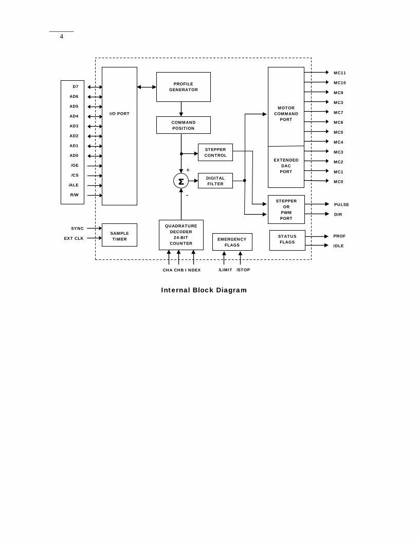
4
Internal Block Diagram
I/O PORT
SAMPLE TIMER
SYNC
EXT CLK
PROFILE
GENERATOR
MOTOR COMMAND
PORT
EXTENDED DAC
PORT
QUADRATURE DECODER
24-BIT COUNTER
CHA CHB I NDEX
MC11
MC10
MC9
MC3
MC7
MC6
MC5
MC4
MC3
MC2
MC1
MC0
STEPPER OR
PWM PORT
PULSE
DIR
COMMAND POSITION
Σ -
+ DIGITAL FILTER
STEPPER CONTROL
EMERGENCY FLAGS
STATUS FLAGS
/LIMIT /STOP
PROF
IDLE
D7
AD6
AD5
AD4
AD3
AD2
AD1
AD0
/OE
/CS
/ALE
R/W
5
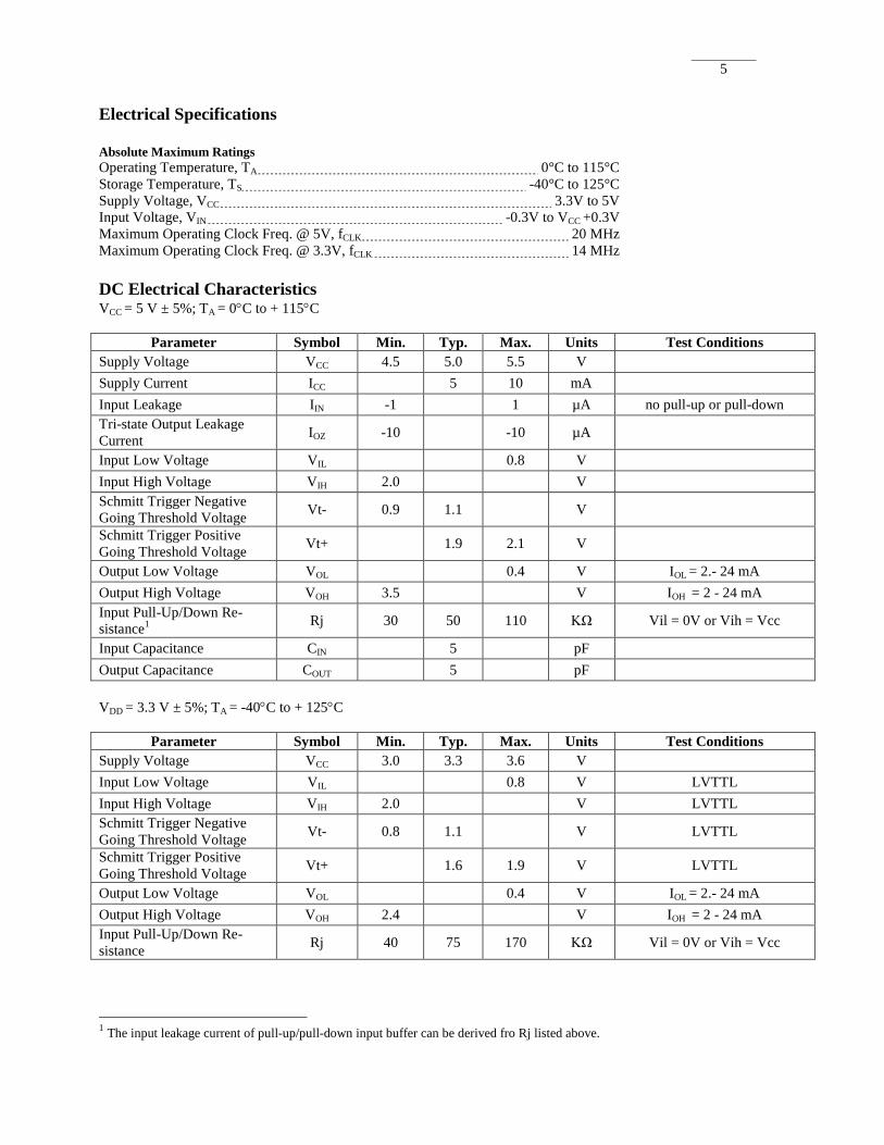
Electrical Specifications Absolute Maximum Ratings Operating Temperature, TA 0°C to 115°C Storage Temperature, TS -40°C to 125°C Supply Voltage, VCC 3.3V to 5V Input Voltage, VIN -0.3V to VCC +0.3V Maximum Operating Clock Freq. @ 5V, fCLK 20 MHz Maximum Operating Clock Freq. @ 3.3V, fCLK 14 MHz DC Electrical Characteristics VCC = 5 V ± 5%; TA = 0°C to + 115°C
Parameter Symbol Min. Typ. Max. Units Test Conditions Supply Voltage VCC 4.5 5.0 5.5 V Supply Current ICC 5 10 mA Input Leakage IIN -1 1 µA no pull-up or pull-down Tri-state Output Leakage Current IOZ -10 -10 µA
Input Low Voltage VIL 0.8 V Input High Voltage VIH 2.0 V Schmitt Trigger Negative Going Threshold Voltage Vt- 0.9 1.1 V
Schmitt Trigger Positive Going Threshold Voltage Vt+ 1.9 2.1 V
Output Low Voltage VOL 0.4 V IOL = 2.- 24 mA Output High Voltage VOH 3.5 V IOH = 2 - 24 mA Input Pull-Up/Down Re-sistance1 Rj 30 50 110 KΩ Vil = 0V or Vih = Vcc
Input Capacitance CIN 5 pF Output Capacitance COUT 5 pF VDD = 3.3 V ± 5%; TA = -40°C to + 125°C
Parameter Symbol Min. Typ. Max. Units Test Conditions Supply Voltage VCC 3.0 3.3 3.6 V Input Low Voltage VIL 0.8 V LVTTL Input High Voltage VIH 2.0 V LVTTL Schmitt Trigger Negative Going Threshold Voltage Vt- 0.8 1.1 V LVTTL
Schmitt Trigger Positive Going Threshold Voltage Vt+ 1.6 1.9 V LVTTL
Output Low Voltage VOL 0.4 V IOL = 2.- 24 mA Output High Voltage VOH 2.4 V IOH = 2 - 24 mA Input Pull-Up/Down Re-sistance Rj 40 75 170 KΩ Vil = 0V or Vih = Vcc
1 The input leakage current of pull-up/pull-down input buffer can be derived fro Rj listed above.
6
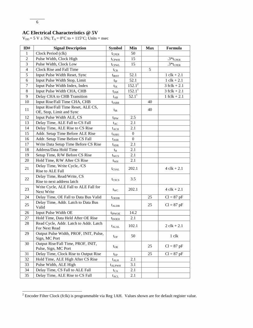
AC Electrical Characteristics @ 5V VDD = 5 V ± 5%; TA = 0°C to + 115°C; Units = nsec ID# Signal Description Symbol Min Max Formula
1 Clock Period (clk) tCPER 50 2 Pulse Width, Clock High tCPWH 15 .3*tCPER 3 Pulse Width, Clock Low tCPWL 15 .3*tCPER 4 Clock Rise and Fall Time tCR 5 5 Input Pulse Width Reset, Sync tIRST 52.1 1 clk + 2.1 6 Input Pulse Width Stop, Limit tIP 52.1 1 clk + 2.1 7 Input Pulse Width Index, Index tIX 152.12 3 fclk + 2.1 8 Input Pulse Width CHA, CHB tIAB 152.11 3 fclk + 2.1 9 Delay CHA to CHB Transition tAB 52.11 1 fclk + 2.1
10 Input Rise/Fall Time CHA, CHB tIABR 40
11 Input Rise/Fall Time Reset, ALE CS, OE, Stop, Limit and Sync tIR 40
12 Input Pulse Width ALE, CS tIPW 2.5 13 Delay Time, ALE Fall to CS Fall tAC 2.1 14 Delay Time, ALE Rise to CS Rise tACH 2.1 15 Addr. Setup Time Before ALE Rise tASR1 0 16 Addr. Setup Time Before CS Fall tASR 0 17 Write Data Setup Time Before CS Rise tSDR 2.1 18 Address/Data Hold Time tH 2.1 19 Setup Time, R/W Before CS Rise tWCS 2.1 20 Hold Time, R/W After CS Rise tWH 2.1
21 Delay Time, Write Cycle, /CS Rise to ALE Fall tCSAL 202.1 4 clk + 2.1
22 Delay Time, Read/Write, CS Rise to next address latch tCSCS 3.5
23 Write Cycle, ALE Fall to ALE Fall for Next Write tWC 202.1 4 clk + 2.1
24 Delay Time, OE Fall to Data Bus Valid tOEDB 25 Cl = 87 pF
25 Delay Time, Addr. Latch to Data Bus Valid tALDB 25 Cl = 87 pF
26 Input Pulse Width OE tIPWOE 14.2 27 Hold Time, Data Held After OE Rise tDOEH 2.1 28 Read Cycle, Addr. Latch to Addr. Latch
For Next Read tALAL 102.1 2 clk + 2.1
29 Output Pulse Width, PROF, INIT, Pulse, Sign, MC Port tOF 50 1 clk
30 Output Rise/Fall Time, PROF, INIT, Pulse, Sign, MC Port tOR 25 Cl = 87 pF
31 Delay Time, Clock Rise to Output Rise tEP 25 Cl = 87 pF 32 Hold Time, ALE High After CS Rise tALH 2.1 33 Pulse Width, ALE High tALPWH 3.1 34 Delay Time, CS Fall to ALE Fall tCA 2.1 35 Delay Time, ALE Rise to CS Fall tACL 2.1
2 Encoder Filter Clock (fclk) is programmable via Reg 1AH. Values shown are for default register value.
7
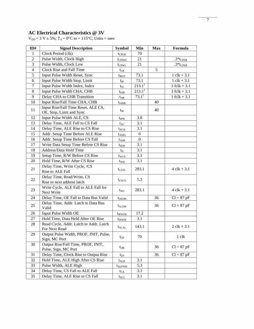
AC Electrical Characteristics @ 3V VDD = 3 V ± 5%; TA = 0°C to + 115°C; Units = nsec ID# Signal Description Symbol Min Max Formula
1 Clock Period (clk) tCPER 70 2 Pulse Width, Clock High tCPWH 21 .3*tCPER 3 Pulse Width, Clock Low tCPWL 21 .3*tCPER 4 Clock Rise and Fall Time tCR 5 5 Input Pulse Width Reset, Sync tIRST 73.1 1 clk + 3.1 6 Input Pulse Width Stop, Limit tIP 73.1 1 clk + 3.1 7 Input Pulse Width Index, Index tIX 213.11 3 fclk + 3.1 8 Input Pulse Width CHA, CHB tIAB 213.11 3 fclk + 3.1 9 Delay CHA to CHB Transition tAB 73.11 1 fclk + 3.1
10 Input Rise/Fall Time CHA, CHB tIABR 40
11 Input Rise/Fall Time Reset, ALE CS, OE, Stop, Limit and Sync tIR 40
12 Input Pulse Width ALE, CS tIPW 3.8 13 Delay Time, ALE Fall to CS Fall tAC 3.1 14 Delay Time, ALE Rise to CS Rise tACH 3.1 15 Addr. Setup Time Before ALE Rise tASR1 0 16 Addr. Setup Time Before CS Fall tASR 0 17 Write Data Setup Time Before CS Rise tSDR 3.1 18 Address/Data Hold Time tH 3.1 19 Setup Time, R/W Before CS Rise tWCS 3.1 20 Hold Time, R/W After CS Rise tWH 3.1
21 Delay Time, Write Cycle, /CS Rise to ALE Fall tCSAL 283.1 4 clk + 3.1
22 Delay Time, Read/Write, CS Rise to next address latch tCSCS 5.3
23 Write Cycle, ALE Fall to ALE Fall for Next Write tWC 283.1 4 clk + 3.1
24 Delay Time, OE Fall to Data Bus Valid tOEDB 36 Cl = 87 pF
25 Delay Time, Addr. Latch to Data Bus Valid tALDB 36 Cl = 87 pF
26 Input Pulse Width OE tIPWOE 17.2 27 Hold Time, Data Held After OE Rise tDOEH 3.1 28 Read Cycle, Addr. Latch to Addr. Latch
For Next Read tALAL 143.1 2 clk + 3.1
29 Output Pulse Width, PROF, INIT, Pulse, Sign, MC Port tOF 70 1 clk
30 Output Rise/Fall Time, PROF, INIT, Pulse, Sign, MC Port tOR 36 Cl = 87 pF
31 Delay Time, Clock Rise to Output Rise tEP 36 Cl = 87 pF 32 Hold Time, ALE High After CS Rise tALH 3.1 33 Pulse Width, ALE High tALPWH 5.3 34 Delay Time, CS Fall to ALE Fall tCA 3.1 35 Delay Time, ALE Rise to CS Fall tACL 3.1
8
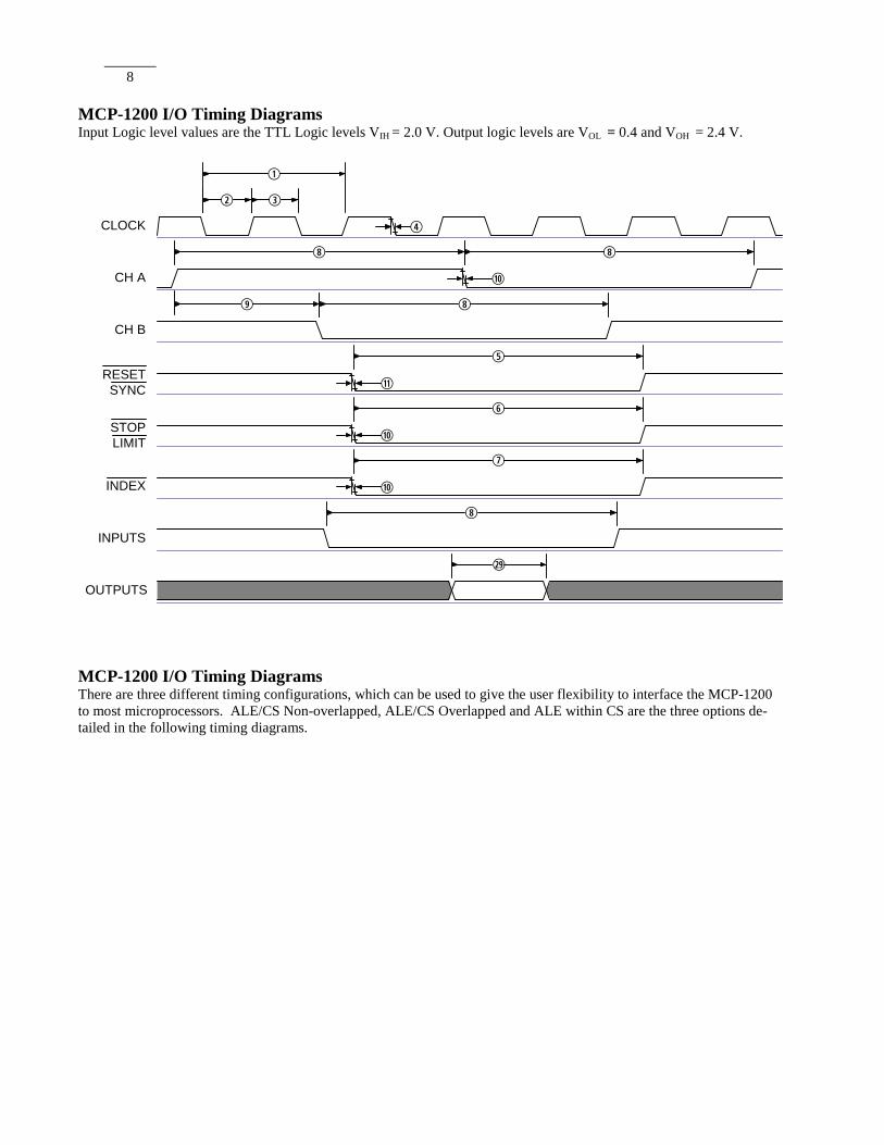
MCP-1200 I/O Timing Diagrams Input Logic level values are the TTL Logic levels VIH = 2.0 V. Output logic levels are VOL = 0.4 and VOH = 2.4 V.
CLOCK
CH A
CH B
RESETSYNC
STOPLIMIT
INDEX
INPUTS
OUTPUTS
i
t
u
i
ii
o
q
w e
2(
y
s
a
a
a
r
MCP-1200 I/O Timing Diagrams There are three different timing configurations, which can be used to give the user flexibility to interface the MCP-1200 to most microprocessors. ALE/CS Non-overlapped, ALE/CS Overlapped and ALE within CS are the three options de-tailed in the following timing diagrams.
9
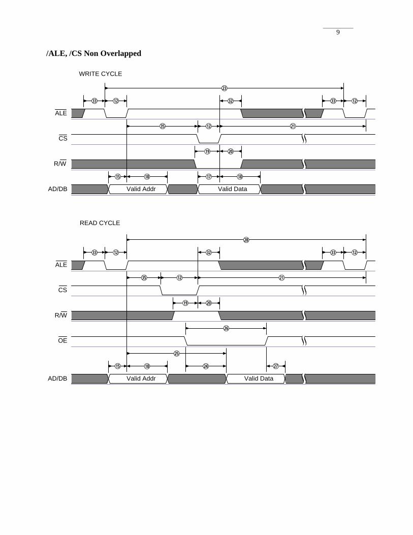
/ALE, /CS Non Overlapped
ALE
CS
R/W
AD/DB
ALE
CS
R/W
OE
AD/DB
Valid Addr Valid Data
Valid Addr Valid Data
READ CYCLE
WRITE CYCLE
2#
1@ 2!
1(
1%
1@3# 3# 1@
1&
3# 3# 1@
2!1@
1(
2*
3@
2%
2^
2$1%
3@1@
2)
2)
1*
1* 1*
2&
3%
3%
10
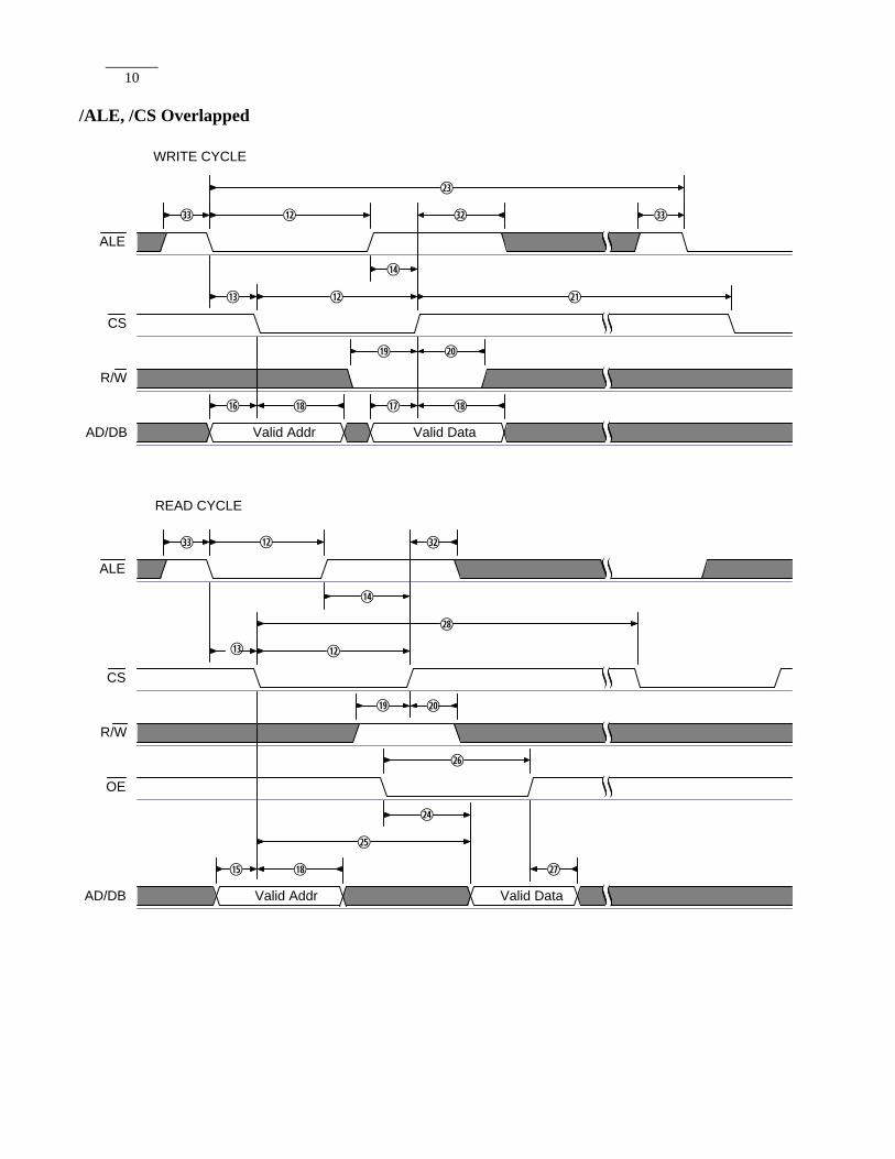
/ALE, /CS Overlapped
ALE
CS
R/W
AD/DB
ALE
CS
R/W
OE
AD/DB
Valid Addr Valid Data
Valid Addr Valid Data
READ CYCLE
WRITE CYCLE
2#
1@
1(
1@3# 3#
1&
3#
1@
1(
3@
2^
2$
1%
3@1@
2)
2)
1*
1*
2&
1#
1^ 1*
1$
2%
1#
2*
1$
2!
11
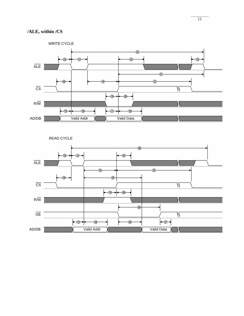
/ALE, within /CS
ALE
CS
R/W
AD/DB
ALE
CS
R/W
OE
AD/DB
Valid Addr Valid Data
Valid Addr Valid Data
READ CYCLE
WRITE CYCLE
2#
1(
1@3# 3#
1&
3#
1(
3@
2^
2$1%
3@1@
2)
2)
1*
1*
2&
1$
1$
1% 1*
2!
2@
2@
2*
3$
3$
2%
12
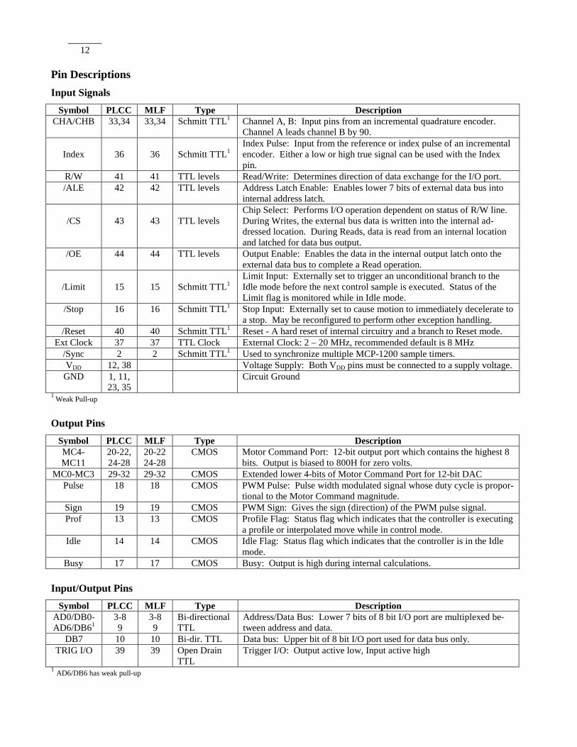
Pin Descriptions Input Signals
Symbol PLCC MLF Type Description CHA/CHB 33,34 33,34 Schmitt TTL1 Channel A, B: Input pins from an incremental quadrature encoder.
Channel A leads channel B by 90.
Index
36
36 Schmitt TTL1
Index Pulse: Input from the reference or index pulse of an incremental encoder. Either a low or high true signal can be used with the Index pin.
R/W 41 41 TTL levels Read/Write: Determines direction of data exchange for the I/O port. /ALE 42 42 TTL levels Address Latch Enable: Enables lower 7 bits of external data bus into
internal address latch.
/CS
43
43 TTL levels
Chip Select: Performs I/O operation dependent on status of R/W line. During Writes, the external bus data is written into the internal ad-dressed location. During Reads, data is read from an internal location and latched for data bus output.
/OE 44 44 TTL levels Output Enable: Enables the data in the internal output latch onto the external data bus to complete a Read operation.
/Limit
15
15
Schmitt TTL1
Limit Input: Externally set to trigger an unconditional branch to the Idle mode before the next control sample is executed. Status of the Limit flag is monitored while in Idle mode.
/Stop 16 16 Schmitt TTL1 Stop Input: Externally set to cause motion to immediately decelerate to a stop. May be reconfigured to perform other exception handling.
/Reset 40 40 Schmitt TTL1 Reset - A hard reset of internal circuitry and a branch to Reset mode. Ext Clock 37 37 TTL Clock External Clock: 2 – 20 MHz, recommended default is 8 MHz
/Sync 2 2 Schmitt TTL1 Used to synchronize multiple MCP-1200 sample timers. VDD 12, 38 Voltage Supply: Both VDD pins must be connected to a supply voltage.
GND 1, 11, 23, 35
Circuit Ground
1 Weak Pull-up Output Pins
Symbol PLCC MLF Type Description MC4-MC11
20-22, 24-28
20-22 24-28
CMOS Motor Command Port: 12-bit output port which contains the highest 8 bits. Output is biased to 800H for zero volts.
MC0-MC3 29-32 29-32 CMOS Extended lower 4-bits of Motor Command Port for 12-bit DAC Pulse 18 18 CMOS PWM Pulse: Pulse width modulated signal whose duty cycle is propor-
tional to the Motor Command magnitude. Sign 19 19 CMOS PWM Sign: Gives the sign (direction) of the PWM pulse signal. Prof 13 13 CMOS Profile Flag: Status flag which indicates that the controller is executing
a profile or interpolated move while in control mode. Idle 14 14 CMOS Idle Flag: Status flag which indicates that the controller is in the Idle
mode. Busy 17 17 CMOS Busy: Output is high during internal calculations.
Input/Output Pins
Symbol PLCC MLF Type Description AD0/DB0- AD6/DB61
3-8 9
3-8 9
Bi-directional TTL
Address/Data Bus: Lower 7 bits of 8 bit I/O port are multiplexed be-tween address and data.
DB7 10 10 Bi-dir. TTL Data bus: Upper bit of 8 bit I/O port used for data bus only. TRIG I/O 39 39 Open Drain
TTL Trigger I/O: Output active low, Input active high
1 AD6/DB6 has weak pull-up

13
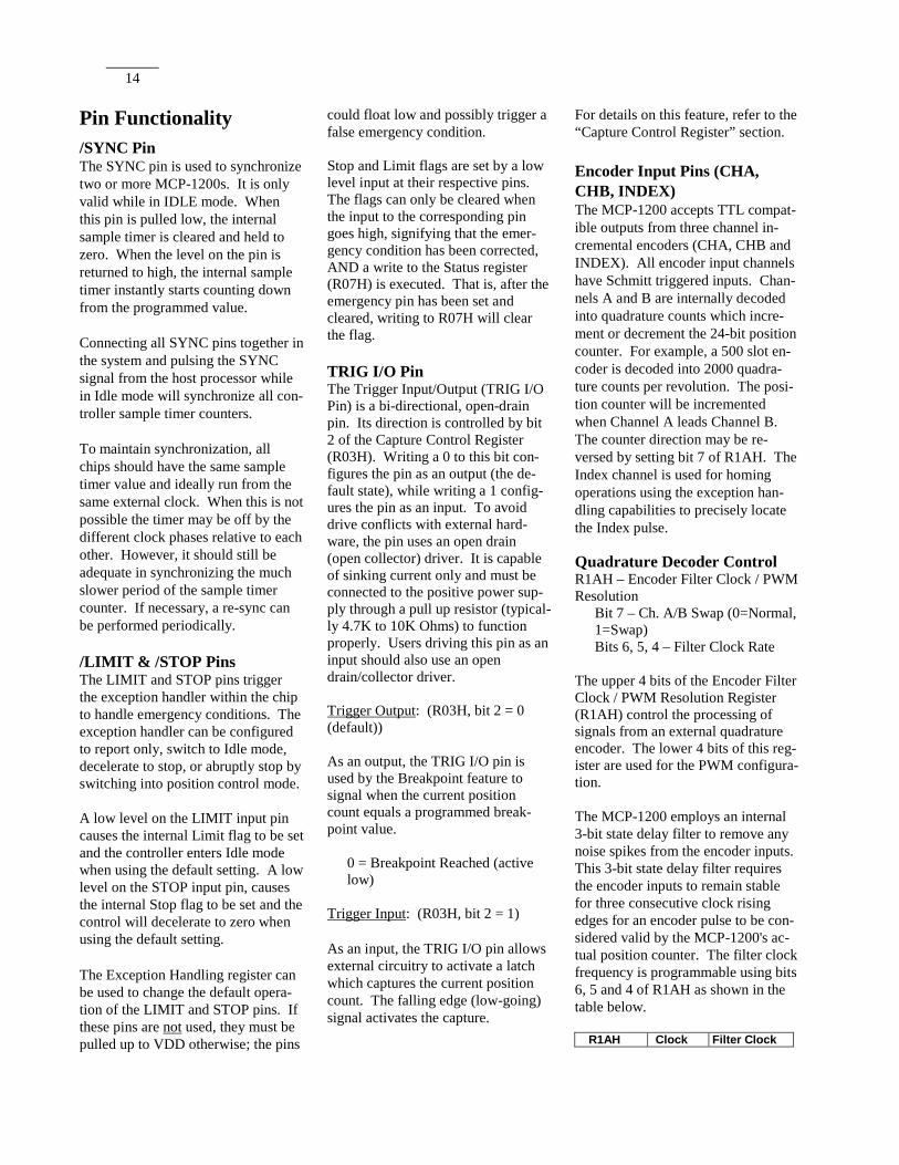
14
Pin Functionality /SYNC Pin The SYNC pin is used to synchronize two or more MCP-1200s. It is only valid while in IDLE mode. When this pin is pulled low, the internal sample timer is cleared and held to zero. When the level on the pin is returned to high, the internal sample timer instantly starts counting down from the programmed value. Connecting all SYNC pins together in the system and pulsing the SYNC signal from the host processor while in Idle mode will synchronize all con-troller sample timer counters. To maintain synchronization, all chips should have the same sample timer value and ideally run from the same external clock. When this is not possible the timer may be off by the different clock phases relative to each other. However, it should still be adequate in synchronizing the much slower period of the sample timer counter. If necessary, a re-sync can be performed periodically. /LIMIT & /STOP Pins The LIMIT and STOP pins trigger the exception handler within the chip to handle emergency conditions. The exception handler can be configured to report only, switch to Idle mode, decelerate to stop, or abruptly stop by switching into position control mode. A low level on the LIMIT input pin causes the internal Limit flag to be set and the controller enters Idle mode when using the default setting. A low level on the STOP input pin, causes the internal Stop flag to be set and the control will decelerate to zero when using the default setting. The Exception Handling register can be used to change the default opera-tion of the LIMIT and STOP pins. If these pins are not used, they must be pulled up to VDD otherwise; the pins
could float low and possibly trigger a false emergency condition. Stop and Limit flags are set by a low level input at their respective pins. The flags can only be cleared when the input to the corresponding pin goes high, signifying that the emer-gency condition has been corrected, AND a write to the Status register (R07H) is executed. That is, after the emergency pin has been set and cleared, writing to R07H will clear the flag. TRIG I/O Pin The Trigger Input/Output (TRIG I/O Pin) is a bi-directional, open-drain pin. Its direction is controlled by bit 2 of the Capture Control Register (R03H). Writing a 0 to this bit con-figures the pin as an output (the de-fault state), while writing a 1 config-ures the pin as an input. To avoid drive conflicts with external hard-ware, the pin uses an open drain (open collector) driver. It is capable of sinking current only and must be connected to the positive power sup-ply through a pull up resistor (typical-ly 4.7K to 10K Ohms) to function properly. Users driving this pin as an input should also use an open drain/collector driver. Trigger Output: (R03H, bit 2 = 0 (default)) As an output, the TRIG I/O pin is used by the Breakpoint feature to signal when the current position count equals a programmed break-point value.
0 = Breakpoint Reached (active low)
Trigger Input: (R03H, bit 2 = 1) As an input, the TRIG I/O pin allows external circuitry to activate a latch which captures the current position count. The falling edge (low-going) signal activates the capture.
For details on this feature, refer to the “Capture Control Register” section. Encoder Input Pins (CHA, CHB, INDEX) The MCP-1200 accepts TTL compat-ible outputs from three channel in-cremental encoders (CHA, CHB and INDEX). All encoder input channels have Schmitt triggered inputs. Chan-nels A and B are internally decoded into quadrature counts which incre-ment or decrement the 24-bit position counter. For example, a 500 slot en-coder is decoded into 2000 quadra-ture counts per revolution. The posi-tion counter will be incremented when Channel A leads Channel B. The counter direction may be re-versed by setting bit 7 of R1AH. The Index channel is used for homing operations using the exception han-dling capabilities to precisely locate the Index pulse. Quadrature Decoder Control R1AH – Encoder Filter Clock / PWM Resolution
Bit 7 – Ch. A/B Swap (0=Normal, 1=Swap) Bits 6, 5, 4 – Filter Clock Rate
The upper 4 bits of the Encoder Filter Clock / PWM Resolution Register (R1AH) control the processing of signals from an external quadrature encoder. The lower 4 bits of this reg-ister are used for the PWM configura-tion. The MCP-1200 employs an internal 3-bit state delay filter to remove any noise spikes from the encoder inputs. This 3-bit state delay filter requires the encoder inputs to remain stable for three consecutive clock rising edges for an encoder pulse to be con-sidered valid by the MCP-1200's ac-tual position counter. The filter clock frequency is programmable using bits 6, 5 and 4 of R1AH as shown in the table below.
R1AH Clock Filter Clock
15
Bits 6,5,4 Divider @20MHz 000 none 20 MHz 001 2 10 MHz 010 4 5 MHz 011 8 2.5 MHz 100 16 1.25 MHz
101, 110, or 111 32 625 KHz
Bit 7 allows swapping of the Channel A and Channel B signals. When CHA leads CHB the position count increases with the default setting of the swap bit. Setting the swap bit to a value of one will result in a count increasing when CHB leads CHA. Swapping channels is sometimes re-quired to get the correct feedback polarity for the servo control loop. Alternatively, the physical CHA and CHB connections could be swapped. Motor Command Port (MC0- MC11) The 12-bit Motor Command port consists of register R08H whose data goes directly to external pins MC4-MC11. The upper 4-bits of R4CH are used as the LSB of the motor com-mand. The Motor Command Port can be read and written to; however, it should be written to only while in Idle mode. During any of the Control modes, the controller writes the mo-tor command directly to R08H and R4CH. This topic is further discussed in the "Motor Command Register" section. Pulse Width Modulation (PWM) Output Port (Pulse, Sign) The PWM port consists of the Pulse and Sign output pins. The PWM port outputs the motor command as a pulse width modulated signal with the correct direction polarity. The modu-lation frequency is programmable using R11H and should be adjusted to around 20 KHz to eliminate audible switching noise. Higher external clock frequencies allow higher switching resolution.
This PWM configuration is further discussed in the "Register Section" under "PWM Motor Command Reg-ister". PROF Pin (Profile Flag) R00H – “Flag Register”
Bit 0 = Profile Control Bit R03H – “Capture Control Register”
Bit 6 = Interpolator Status on PROF pin (1 = active) R07H – “Status Register”
Bit 4 = In-mode Flag (1= In Pro-file, Velocity, or Interpolation Mode) The PROF Pin is internally connected to software flag bit 4 in the Status Register. Both the Pin and the Status indicate motion in Position Profile, Velocity or Interpolation modes. When the MCP-1200 begins a move, this flag is set by the controller (a high level appears on the pin), indi-cating the move is in progress. When the MCP-1200 finishes the move, the controller clears this flag. In Velocity mode, the pin is active for non-zero velocity commands. In Interpolation mode, the pin is active during inter-polation. Note that the instant the flag is cleared may not be the same instant the motor stops. The flag indicates the completion of the command pro-file, not the actual profile. If the mo-tor is stalled during the move, or can-not physically keep up with the move, the flag will be cleared before the move is finished. The Status register bit 4 is an “In-mode” flag meaning that it is asserted in all profile modes (Profile, Veloci-ty, and Interpolation) signifying the chip is controlling motor movement. Additionally, this “In-Mode” bit drives the PROF pin. The PROF pin can be used to drive external circuitry (such as safety shields) that would be activated during motor movement. Optionally, the PROF pin can be used to indicate the interpolator status when using Position or Velocity In-
terpolation Mode. To select this function of the PROF pin, bit 6 of the Capture Control Register (R03H) must be set. For more information on this use refer to the Interpolation mode descriptions. Note that even if this control bit is set, the PROF pin will return to its “In-Mode” function when the chip is not in an interpola-tion mode. IDLE Pin This pin indicates that the MCP- 1200 is in IDLE mode, waiting to begin control mode. This pin is in-ternally connected to the software flag bit 5 in the Status Register R07H. This flag is also represented by bit 1 in the flag Register (R00H). The Idle pin is typically used as an enable signal for the motor driver. BUSY Pin The Busy pin is an output that goes high when the chip is performing internal computations. Bit 0 of the Status register is high (1) when the chip is Busy. The chip is waiting for the next sample time when not Busy. In most cases, the host system may read or write to registers at any time without concern of the state of Busy. Synchronization with the Busy status is important for some multi-register values that may be changed during the Busy cycle (such as, Position Er-ror and Actual Velocity). Additional-ly, if the host system wishes to log data values such as Position Error, the Busy signal is useful for triggering the register reads. Writing or reading multiple register values may also need to be synchronized with the Busy signal to insure that the value is stable for all bytes. This becomes important during interpolation modes or executing “on-the-fly” motion modifications. Providing both a hardware Busy pin and a Status register flag provides maximum flexibility for interfacing to the MCP-1200 chip. In some ap-
16
plications using the hardware pin can provide an automated synchroniza-tion with the chip’s sampling rate.
Operation of the MCP-1200 Registers Two banks of 64 (128) 8-bit registers controls the MCP-1200 operation. In order to get access to the upper bank the extended addressing bit of the Advanced control register must be set. The default maintains compati-bility with the MCP-1100 which can only address 64 registers. The user-accessible registers are listed in the Register Reference Table on the following pages. The register number is also the address as seen from the MCP-1200. These registers contain command and configuration information necessary to properly run the motion controller. The Opera-tional Flow Chart shows a functional block diagram of the MCP-1200 which indicates the structure and flow of the chips firmware.
17
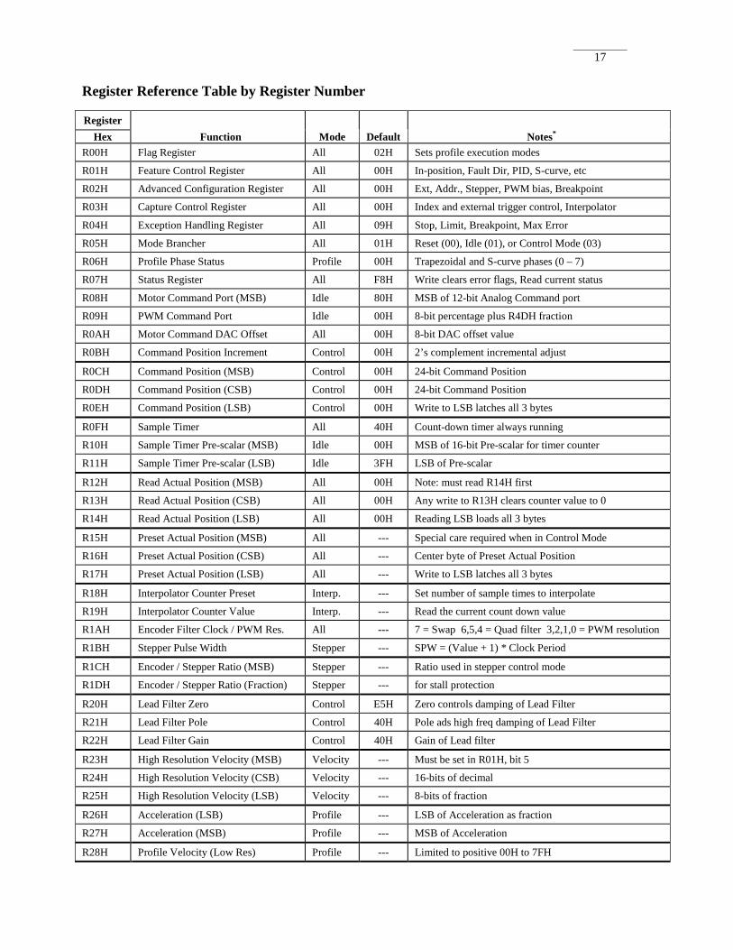
Register Reference Table by Register Number Register
Hex Function Mode Default Notes* R00H Flag Register All 02H Sets profile execution modes
R01H Feature Control Register All 00H In-position, Fault Dir, PID, S-curve, etc
R02H Advanced Configuration Register All 00H Ext, Addr., Stepper, PWM bias, Breakpoint
R03H Capture Control Register All 00H Index and external trigger control, Interpolator
R04H Exception Handling Register All 09H Stop, Limit, Breakpoint, Max Error
R05H Mode Brancher All 01H Reset (00), Idle (01), or Control Mode (03)
R06H Profile Phase Status Profile 00H Trapezoidal and S-curve phases (0 – 7)
R07H Status Register All F8H Write clears error flags, Read current status
R08H Motor Command Port (MSB) Idle 80H MSB of 12-bit Analog Command port
R09H PWM Command Port Idle 00H 8-bit percentage plus R4DH fraction
R0AH Motor Command DAC Offset All 00H 8-bit DAC offset value
R0BH Command Position Increment Control 00H 2’s complement incremental adjust
R0CH Command Position (MSB) Control 00H 24-bit Command Position
R0DH Command Position (CSB) Control 00H 24-bit Command Position
R0EH Command Position (LSB) Control 00H Write to LSB latches all 3 bytes
R0FH Sample Timer All 40H Count-down timer always running
R10H Sample Timer Pre-scalar (MSB) Idle 00H MSB of 16-bit Pre-scalar for timer counter
R11H Sample Timer Pre-scalar (LSB) Idle 3FH LSB of Pre-scalar
R12H Read Actual Position (MSB) All 00H Note: must read R14H first
R13H Read Actual Position (CSB) All 00H Any write to R13H clears counter value to 0
R14H Read Actual Position (LSB) All 00H Reading LSB loads all 3 bytes
R15H Preset Actual Position (MSB) All --- Special care required when in Control Mode
R16H Preset Actual Position (CSB) All --- Center byte of Preset Actual Position
R17H Preset Actual Position (LSB) All --- Write to LSB latches all 3 bytes
R18H Interpolator Counter Preset Interp. --- Set number of sample times to interpolate
R19H Interpolator Counter Value Interp. --- Read the current count down value
R1AH Encoder Filter Clock / PWM Res. All --- 7 = Swap 6,5,4 = Quad filter 3,2,1,0 = PWM resolution
R1BH Stepper Pulse Width Stepper --- SPW = (Value + 1) * Clock Period
R1CH Encoder / Stepper Ratio (MSB) Stepper --- Ratio used in stepper control mode
R1DH Encoder / Stepper Ratio (Fraction) Stepper --- for stall protection
R20H Lead Filter Zero Control E5H Zero controls damping of Lead Filter
R21H Lead Filter Pole Control 40H Pole ads high freq damping of Lead Filter
R22H Lead Filter Gain Control 40H Gain of Lead filter
R23H High Resolution Velocity (MSB) Velocity --- Must be set in R01H, bit 5
R24H High Resolution Velocity (CSB) Velocity --- 16-bits of decimal
R25H High Resolution Velocity (LSB) Velocity --- 8-bits of fraction
R26H Acceleration (LSB) Profile --- LSB of Acceleration as fraction
R27H Acceleration (MSB) Profile --- MSB of Acceleration
R28H Profile Velocity (Low Res) Profile --- Limited to positive 00H to 7FH
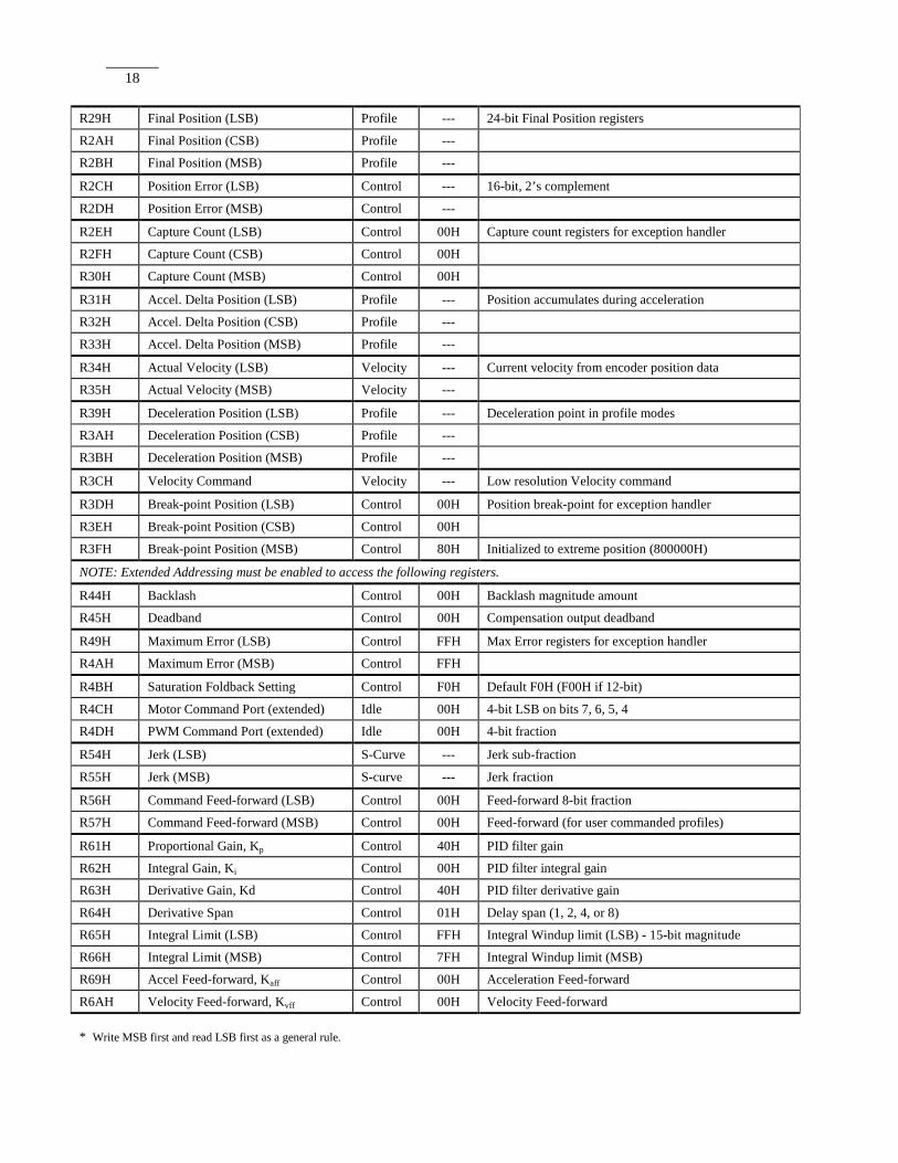
18
R29H Final Position (LSB) Profile --- 24-bit Final Position registers
R2AH Final Position (CSB) Profile ---
R2BH Final Position (MSB) Profile ---
R2CH Position Error (LSB) Control --- 16-bit, 2’s complement
R2DH Position Error (MSB) Control ---
R2EH Capture Count (LSB) Control 00H Capture count registers for exception handler
R2FH Capture Count (CSB) Control 00H
R30H Capture Count (MSB) Control 00H
R31H Accel. Delta Position (LSB) Profile --- Position accumulates during acceleration
R32H Accel. Delta Position (CSB) Profile ---
R33H Accel. Delta Position (MSB) Profile ---
R34H Actual Velocity (LSB) Velocity --- Current velocity from encoder position data
R35H Actual Velocity (MSB) Velocity ---
R39H Deceleration Position (LSB) Profile --- Deceleration point in profile modes
R3AH Deceleration Position (CSB) Profile ---
R3BH Deceleration Position (MSB) Profile ---
R3CH Velocity Command Velocity --- Low resolution Velocity command
R3DH Break-point Position (LSB) Control 00H Position break-point for exception handler
R3EH Break-point Position (CSB) Control 00H
R3FH Break-point Position (MSB) Control 80H Initialized to extreme position (800000H)
NOTE: Extended Addressing must be enabled to access the following registers.
R44H Backlash Control 00H Backlash magnitude amount
R45H Deadband Control 00H Compensation output deadband
R49H Maximum Error (LSB) Control FFH Max Error registers for exception handler
R4AH Maximum Error (MSB) Control FFH
R4BH Saturation Foldback Setting Control F0H Default F0H (F00H if 12-bit)
R4CH Motor Command Port (extended) Idle 00H 4-bit LSB on bits 7, 6, 5, 4
R4DH PWM Command Port (extended) Idle 00H 4-bit fraction
R54H Jerk (LSB) S-Curve --- Jerk sub-fraction
R55H Jerk (MSB) S-curve --- Jerk fraction
R56H Command Feed-forward (LSB) Control 00H Feed-forward 8-bit fraction
R57H Command Feed-forward (MSB) Control 00H Feed-forward (for user commanded profiles)
R61H Proportional Gain, Kp Control 40H PID filter gain
R62H Integral Gain, Ki Control 00H PID filter integral gain
R63H Derivative Gain, Kd Control 40H PID filter derivative gain
R64H Derivative Span Control 01H Delay span (1, 2, 4, or 8)
R65H Integral Limit (LSB) Control FFH Integral Windup limit (LSB) - 15-bit magnitude
R66H Integral Limit (MSB) Control 7FH Integral Windup limit (MSB)
R69H Accel Feed-forward, Kaff Control 00H Acceleration Feed-forward
R6AH Velocity Feed-forward, Kvff Control 00H Velocity Feed-forward * Write MSB first and read LSB first as a general rule.
19
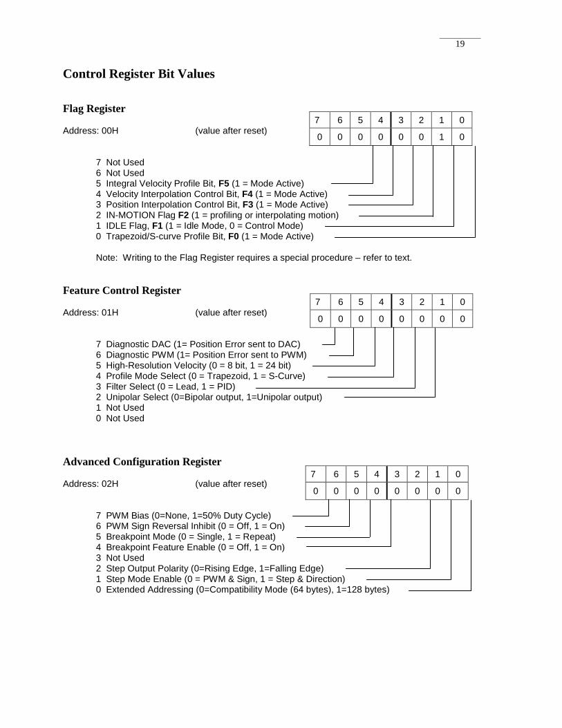
Control Register Bit Values Flag Register Address: 00H (value after reset)
7 Not Used 6 Not Used
5 Integral Velocity Profile Bit, F5 (1 = Mode Active) 4 Velocity Interpolation Control Bit, F4 (1 = Mode Active) 3 Position Interpolation Control Bit, F3 (1 = Mode Active) 2 IN-MOTION Flag F2 (1 = profiling or interpolating motion) 1 IDLE Flag, F1 (1 = Idle Mode, 0 = Control Mode) 0 Trapezoid/S-curve Profile Bit, F0 (1 = Mode Active) Note: Writing to the Flag Register requires a special procedure – refer to text. Feature Control Register Address: 01H (value after reset)
7 Diagnostic DAC (1= Position Error sent to DAC) 6 Diagnostic PWM (1= Position Error sent to PWM) 5 High-Resolution Velocity (0 = 8 bit, 1 = 24 bit) 4 Profile Mode Select (0 = Trapezoid, 1 = S-Curve) 3 Filter Select (0 = Lead, 1 = PID) 2 Unipolar Select (0=Bipolar output, 1=Unipolar output) 1 Not Used 0 Not Used
Advanced Configuration Register Address: 02H (value after reset)
7 PWM Bias (0=None, 1=50% Duty Cycle) 6 PWM Sign Reversal Inhibit (0 = Off, 1 = On) 5 Breakpoint Mode (0 = Single, 1 = Repeat) 4 Breakpoint Feature Enable (0 = Off, 1 = On) 3 Not Used 2 Step Output Polarity (0=Rising Edge, 1=Falling Edge) 1 Step Mode Enable (0 = PWM & Sign, 1 = Step & Direction) 0 Extended Addressing (0=Compatibility Mode (64 bytes), 1=128 bytes)
7 6 5 4 3 2 1 0
0 0 0 0 0 0 1 0
7 6 5 4 3 2 1 0
0 0 0 0 0 0 0 0
7 6 5 4 3 2 1 0
0 0 0 0 0 0 0 0
20
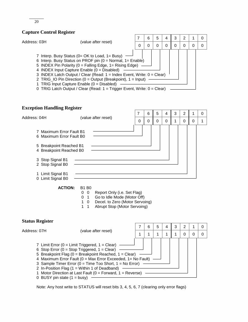
Capture Control Register Address: 03H (value after reset)
7 Interp. Busy Status (0= OK to Load, 1= Busy) 6 Interp. Busy Status on PROF pin (0 = Normal, 1= Enable) 5 INDEX Pin Polarity (0 = Falling Edge, 1= Rising Edge) 4 INDEX Input Capture Enable (0 = Disabled) 3 INDEX Latch Output / Clear (Read: 1 = Index Event, Write: 0 = Clear) 2 TRIG_IO Pin Direction (0 = Output (Breakpoint), 1 = Input) 1 TRIG Input Capture Enable (0 = Disabled) 0 TRIG Latch Output / Clear (Read: 1 = Trigger Event, Write: 0 = Clear)
Exception Handling Register Address: 04H (value after reset)
7 Maximum Error Fault B1 6 Maximum Error Fault B0
5 Breakpoint Reached B1 4 Breakpoint Reached B0
3 Stop Signal B1 2 Stop Signal B0
1 Limit Signal B1 0 Limit Signal B0
ACTION: B1 B0 0 0 Report Only (i.e. Set Flag) 0 1 Go to Idle Mode (Motor Off) 1 0 Decel. to Zero (Motor Servoing) 1 1 Abrupt Stop (Motor Servoing) Status Register Address: 07H (value after reset)
7 Limit Error (0 = Limit Triggered, 1 = Clear) 6 Stop Error (0 = Stop Triggered, 1 = Clear) 5 Breakpoint Flag (0 = Breakpoint Reached, 1 = Clear) 4 Maximum Error Fault (0 = Max Error Exceeded, 1= No Fault) 3 Sample Timer Error (0 = Time Too Short, 1 = No Error) 2 In-Position Flag (1 = Within 1 of Deadband) 1 Motor Direction at Last Fault (0 = Forward, 1 = Reverse) 0 BUSY pin state (1 = busy)
Note: Any host write to STATUS will reset bits 3, 4, 5, 6, 7 (clearing only error flags)
7 6 5 4 3 2 1 0
0 0 0 0 0 0 0 0
7 6 5 4 3 2 1 0
0 0 0 0 1 0 0 1
7 6 5 4 3 2 1 0
1 1 1 1 1 0 0 0

21
Register Descriptions and Op-eration Flag Register (R00H) The Flag register contains flags F0 through F5. This register is a read/write register. Each flag is set and cleared by writing an 8-bit data word to R00H. When writing to R00H, the upper four bits are ignored by the MCP-1200, bits 0, 1, 2 specify the flag address, and bit 3 specifies whether to set (bit = 1) or clear (bit=0) the addressed flag. This method guarantees that only one flag can be set or cleared at a time. When more than one flag has been set, the operation will be as defined in the Operation Flowchart given on page 34. It is therefore recommended that each control bit be cleared before switching profile modes. Flag Descriptions F0 – Position Profile (bit 0): Set to 1 to execute a Position Profile such as trapezoidal or S-curve profiles. The controller resets the bit when the move has completed. The status of F0 can also be monitored at the PROF pin. Fl - Idle Flag (bit 1): set/cleared by the MCP-1200 to indicate execution of Idle mode. The status of F1 can be monitored using this flag and at the Idle output pin. The user should not attempt to set or clear F1. F2 – Profile Mode Flag (bit 2): pro-vides acknowledgement that chip is in a profile mode. This may be position, velocity or interpolation modes. In the case of a Position Profile, this flag duplicates F0 status. F3 - Position Interpolation Control (bit 3): Set to 1 to execute Position Inter-polation. F4 - Velocity Interpolation Con-trol (bit 4): Set to 1 to execute Velocity Interpolation. F5 - Integral Velocity Control (bit 5): Set to 1 to specify Integral Velocity Control. F6, F7 - Bits 6 and 7 are not used.
Writing to the Flag Register When writing to the flag register, only the lower four bits are used. Bit 3 indicates whether to set or clear a certain flag, and bits 2, l, and 0 indicate the particular flag. The following table shows the bit map of the Flag register:
Bit Number Function 7-4 3 2 1 0
Don’t Care 1/0 = set/clr AD2 AD1 AD0
The following table outlines the possible writes to the Flag Regis-ter:
Flag Set Clear F0 F1 F2 F3 F4 F5
08H -
0AH 0BH 0CH 0DH
00H -
02H 03H 04H 05H
Reading the Flag Register Reading register R00H returns the status of the flags in bits 0 to 5. For example, if bit 0 is set (logic 1) then flag F0 is set. If bit 4 is set, then flag F4 is set. If bits 0 and 5 are set, then both flags F0 and F5 are set. The following table delineates the Flag Register.
Bit Number
Flag Register 0 = clr, 1 = set
8-6 5 4 3 2 1 0
Don’t Care F5 F4 F3 F2 F1 F0
Feature Control Register (R01H) Bit 0 – Not Used
Bit 1 – Not Used
Bit 2 – Unipolar Select (0 = Bipolar Output, 1 = Unipolar Output)
See following section “Motor Command Register”.
Bit 3 – Filter Select (0 = Lead, 1 = PID)
See following sections “Lead-lead Filter Register” and “PID Filter Registers”.
Bit 4 – Profile Mode Select (0 = Trapezoid, 1 = S-Curve)
See following sections “Trapezoid Profile Mode” and “S-Curve Pro-file”.
Bit 5 – High Resolution Velocity (0 = 8 bit, 1 = 24 bit)
See following section “High-Res Velocity Registers”.
Bit 6 – Diagnostic Output to PWM (0 = Normal PWM, 1 = Position Error output to PWM)
See below:
Bit 7 – Diagnostic Output to DAC (0 = Normal DAC, 1 = Position Error output to PWM)
This feature allows the direct out-put of Position Error data. This information can be useful in “tun-ing” filter parameters by present-ing the difference between the command position and the actual position in real time.
A user with a system using the PWM output to drive a motor could output the position error on the DAC output pins and monitor the data with an oscilloscope if digital-to-analog circuitry is used. Similarly, for a system using the DAC to drive the motor, the user could output the position error data to the PWM pin and monitor
22
the data with an oscilloscope em-ploying a low-pass filter.
In either case, information is pre-sented on the selected output and updated on each sample cycle. Filter response to step inputs, ve-locity commands, or profile moves can be graphically dis-played. This provides near instan-taneous feedback to changes in filter parameters, and greatly im-proves the speed and accuracy of system tuning. Adv. Configuration Register (R02H) The host can access the Advanced configuration Register at any time. The extended address bit is used for compatibility with the 64 byte addressing of the HCTL-1100. New designs may want to extend the chip to 128 bytes of addresses to access additional features. The controller can be configured for a stepper motor which accepts step and direction pulses. The Step Polarity may be set to rising edge or falling edge for compati-bility with the driver interface. The breakpoint features can be enabled to output an exception when an event is triggered. The exception may be handled as a one-time occurrence or as a repeti-tive delta displacement. Detailed information on the Capture Con-trol Register (R03H) and the Ex-ception Handling Register (R04H) are given in the following sec-tions. The PWM format can be config-ured for 50% bias. A 50% duty cycle is equivalent to a 0 volt mo-tor command. The 50% bias for-mat is also useful for displaying the error performance on an oscil-loscope. Detailed information on the PWM Command Register (R09H) is given in that section.
Capture Control Register (R03H) The Capture Control Register con-figures the capture of the position count based on signal from the INDEX pin or the TRIG I/O pin. The TRIG I/O is activated on the falling edge whereas the INDEX may either be configured for the falling or rising edge (Bit 5). En-able control bits can activate ei-ther (or both) source signals. Each signal has an independent latched monitor bit in the Capture Control Register which may be independently cleared. Bit 7 is used for the Position and Velocity Interpolation features. This bit indicates the status of a latch that is set when the host writes new position (or velocity) data, and cleared when the core has used the data. If bit 6 is set, the status from bit 7 is output on the PROF pin while in either in-terpolation mode. Exception Handling Register (R04H) See Also: R46H – Forced Exception Regis-ter Each error condition can be han-dled in one of four ways. The Exception Handling Register (R04H) allows the user to specify what action should be taken when error conditions are received on the Limit or Stop pin, when a Breakpoint is reached, or when the programmed value for Maxi-mum Error is exceeded. Two bits are used for each error condition.
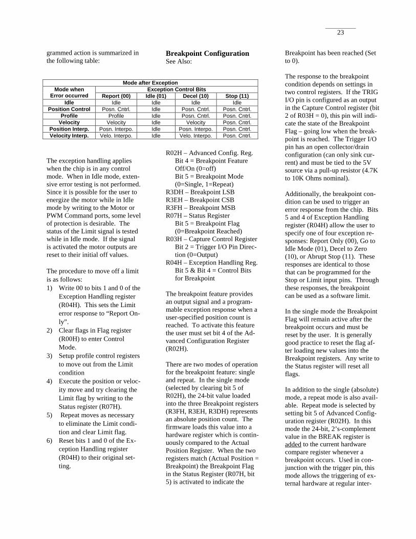
The four exception actions are encoded into the 2-bit values as follows: 00 = Report Only (Set flag/bit, but take no action) 01 = Go to Idle Mode (Motor out-put off) 10 = Decel. to Zero (Decelerate at programmed accel. rate (R26H & R27H)) 11 = Abrupt Stop (Motor servo at current location) In some cases, the selected action is limited by the current opera-tional mode. “Decel. to Zero” will result in deceleration at the programmed acceleration rate in the Profile or Velocity mode. However, in Position Control and Position Interpolation modes, an Abrupt Stop will result (since the-se modes do not calculate acceler-ation). In Interpolated Velocity mode, a “Decel. to Zero” com-mand will load zero into the ve-locity registers with the decelera-tion rate determined by the number of samples selected for the interpolation segment. In addition to responding to error events, an exception can be forced by the host computer. By setting bits zero and/or one of the forced exception register (R46H), the host can create a “software” ex-ception. The same two-bit encod-ing applies (i.e. 01=Idle, 10=Decel, 11=Stop). The system response will be identical to that produced by a system error. Once the exception response is com-plete, the Forced Exception regis-ter must be cleared to zero to re-turn to normal operation. The default settings for the Excep-
tion Handling Registers are sum-marized below. The mode entered after completion of the pro-
Error Condition: Max Error Breakpoint Stop Signal Limit Signal R04H bit: 7 6 5 4 3 2 1 0 Value at Reset: 0 0 0 0 1 0 0 1
23
grammed action is summarized in the following table:
The exception handling applies when the chip is in any control mode. When in Idle mode, exten-sive error testing is not performed. Since it is possible for the user to energize the motor while in Idle mode by writing to the Motor or PWM Command ports, some level of protection is desirable. The status of the Limit signal is tested while in Idle mode. If the signal is activated the motor outputs are reset to their initial off values. The procedure to move off a limit is as follows: 1) Write 00 to bits 1 and 0 of the
Exception Handling register (R04H). This sets the Limit error response to “Report On-ly”.
2) Clear flags in Flag register (R00H) to enter Control Mode.
3) Setup profile control registers to move out from the Limit condition
4) Execute the position or veloc-ity move and try clearing the Limit flag by writing to the Status register (R07H).
5) Repeat moves as necessary to eliminate the Limit condi-tion and clear Limit flag.
6) Reset bits 1 and 0 of the Ex-ception Handling register (R04H) to their original set-ting.
Breakpoint Configuration See Also:
R02H – Advanced Config. Reg. Bit 4 = Breakpoint Feature
Off/On (0=off) Bit 5 = Breakpoint Mode
(0=Single, 1=Repeat) R3DH – Breakpoint LSB R3EH – Breakpoint CSB R3FH – Breakpoint MSB R07H – Status Register Bit 5 = Breakpoint Flag
(0=Breakpoint Reached) R03H – Capture Control Register Bit 2 = Trigger I/O Pin Direc-
tion (0=Output) R04H – Exception Handling Reg.
Bit 5 & Bit 4 = Control Bits for Breakpoint
The breakpoint feature provides an output signal and a program-mable exception response when a user-specified position count is reached. To activate this feature the user must set bit 4 of the Ad-vanced Configuration Register (R02H). There are two modes of operation for the breakpoint feature: single and repeat. In the single mode (selected by clearing bit 5 of R02H), the 24-bit value loaded into the three Breakpoint registers (R3FH, R3EH, R3DH) represents an absolute position count. The firmware loads this value into a hardware register which is contin-uously compared to the Actual Position Register. When the two registers match (Actual Position = Breakpoint) the Breakpoint Flag in the Status Register (R07H, bit 5) is activated to indicate the
Breakpoint has been reached (Set to 0). The response to the breakpoint condition depends on settings in two control registers. If the TRIG I/O pin is configured as an output in the Capture Control register (bit 2 of R03H = 0), this pin will indi-cate the state of the Breakpoint Flag – going low when the break-point is reached. The Trigger I/O pin has an open collector/drain configuration (can only sink cur-rent) and must be tied to the 5V source via a pull-up resistor (4.7K to 10K Ohms nominal). Additionally, the breakpoint con-dition can be used to trigger an error response from the chip. Bits 5 and 4 of Exception Handling register (R04H) allow the user to specify one of four exception re-sponses: Report Only (00), Go to Idle Mode (01), Decel to Zero (10), or Abrupt Stop (11). These responses are identical to those that can be programmed for the Stop or Limit input pins. Through these responses, the breakpoint can be used as a software limit. In the single mode the Breakpoint Flag will remain active after the breakpoint occurs and must be reset by the user. It is generally good practice to reset the flag af-ter loading new values into the Breakpoint registers. Any write to the Status register will reset all flags. In addition to the single (absolute) mode, a repeat mode is also avail-able. Repeat mode is selected by setting bit 5 of Advanced Config-uration register (R02H). In this mode the 24-bit, 2’s-complement value in the BREAK register is added to the current hardware compare register whenever a breakpoint occurs. Used in con-junction with the trigger pin, this mode allows the triggering of ex-ternal hardware at regular inter-
Mode after Exception Mode when
Error occurred Exception Control Bits
Report (00) Idle (01) Decel (10) Stop (11) Idle Idle Idle Idle Idle
Position Control Posn. Cntrl. Idle Posn. Cntrl. Posn. Cntrl. Profile Profile Idle Posn. Cntrl. Posn. Cntrl.
Velocity Velocity Idle Velocity Posn. Cntrl. Position Interp. Posn. Interpo. Idle Posn. Interpo. Posn. Cntrl. Velocity Interp. Velo. Interpo. Idle Velo. Interpo. Posn. Cntrl.
24
vals without program intervention. When a breakpoint is reached the Breakpoint Flag and TRIG I/O pin (if enabled) are activated (active low). Since this is controlled by the hardware, it is almost instan-taneous. Within one sample time, the firmware will add the Break-point register value to the current breakpoint and automatically de-activate the Flag and pin. The length of the trigger pulse will vary depending when in the sam-ple cycle the breakpoint occurs. It may be as short as 67 clock cycles or as long as a sample timer inter-val. In any case, the falling edge of the pulse signifies the time when the actual position equals the breakpoint value. Usage Example: Assume that the trigger output is used to synchronize external cir-cuitry that must be activated at specific position counts. Say that the position is currently at zero and that we want our first trigger at position count 15000 followed by a trigger every 2500 counts. 1. Clear bits 5 and 4 of R04H.
This sets the exception action to “Report Only” (we do not want to stop or change modes when a breakpoint is encoun-tered).
2. Clear bit 2 of R03H. This configures the Trigger I/O pin as an output.
3. Clear bit 5 and Set bit 4 of R02H. This turns on the breakpoint feature and selects Single Mode.
4. Load the first trigger position (15000) into the BREAK reg-isters. 15000 = 003A98 hex so, BREAK3 = 00h, BREAK2 = 3Ah, BREAK1 = 98h.
5. Wait at least one sample time while the firmware transfers the break value into the hardware register.
6. Reset the breakpoint flag by writing to STATUS. This flag may have been set if the current position equaled the old breakpoint.
7. Set bit 5 of R02H to select repeat breakpoint mode.
8. Load the repeat count value (2500) into the BREAK regis-ters. 2500 = 0009C4h so, BREAK2 = 00h, BREAK1 = 09h, BREAK0 = C4h. Note that this value will not be added to the count until the first breakpoint is reached.
9. Now start a positive move in whatever mode is desired (Position Control, Profile, Velocity, or Interpolation). Without any intervention, the trigger pin will pulse low when the position count reaches 15000, 17500, 20000, 22500, and so on.
Position Capture R03H – Capture Control Register
Bit 5 = INDEX Pin Polarity (0 = Falling Edge, 1= Rising Edge) Bit 4 = INDEX Input Capture Enable (0 = Disabled) Bit 3 = INDEX Latch Output / Clear (Read: 1 = Index Event, Write: 0 = Clear) Bit 2 = TRIG_IO Pin Direction (0 = Output (Breakpoint), 1 = Input) Bit 1 = TRIG Input Capture Enable (0 = Disabled) Bit 0 = TRIG Latch Output / Clear (Read: 1 = Trigger Event, Write: 0 = Clear)
R2EH – Capture Position LSB R2FH – Capture Position CSB R30H – Capture Position MSB The Position Capture feature latches the current actual position count at the instant that a signal is received on the Trigger I/O pin or the Index pin. The 24-bit captured position count value is stored in three registers for host access.
Bits within the Capture Control Register (R03H) control all as-pects of this function. Bit 5 and bit 1 enable the Index pin and the Trigger I/O pin respectively as sources for the capture signal. The two sources may be enabled individually or both may be ena-bled at the same time. The TRIG I/O pin direction is controlled by bit 2. This bit must be set to use the pin as a source for the capture command. Since the pin can also be used as an open collector/drain output by the Breakpoint function, it is im-portant to drive it with an open collector (or open drain) source and provide a passive pull-up re-sistor on the line. This will pre-vent the possibility of driver con-flicts. A falling-edge transition on the TRIG I/O pin will activate the Trigger latch, causing bit 0 of Capture Control register to be set high. If the Trigger Input Capture Enable bit is active (bit 1 = 1), the position count will be captured. The host can examine the latch bit (bit 0) to determine when a cap-ture signal has taken place. The host can than read the captured position count from registers R2EH, R2FH, and R30H. Since these registers hold a static value, they may be read in any order. To “re-arm” the capture feature the host must clear the active latch output, in this case by writing a 0 to bit-0 of Capture Control Regis-ter (R03H). The Index input pin works in a similar fashion. However, bit 5 of Capture Control register (R03H) allows the selection of falling-edge or rising-edge sensitivity to transitions on the Index pin. The selected transition will activate the Index latch, causing bit 3 to be set. If the Index Input Capture Enable bit is set (bit 4 = 1) the position
25
count will be captured. After the host reads the captured values it must write a 0 to bit 4 to reset the capture latch. The latches for the Index and Trigger I/O pins (which output to bits 3 and 0) are always active even if their respective capture enable bits are disabled. This allows host monitoring of transi-tions on the pins without neces-sarily capturing the current posi-tion count. At power-up, all associated regis-ters are reset to zero. However, the register content is unaffected by a soft reset. Mode Brancher (R05H) The Mode Brancher switches to the preprogrammed functions of the controller. The Mode Brancher is used along with the control flags F0, F3, and F5 in the Flag register (R00H) to change control modes. The user can write any of the following four com-mands to the Mode Brancher.
Value written to
R05H
Action 00H 01H 02H 03H
Software Reset Enter Idle Mode Halt Motion Enter Control Mode (only from Idle Mode)
These Commands are discussed in more detail in the "Operation Flowchart" section. Status Register (R07H) Each bit of the Status register de-codes the MCP-1200 current sta-tus. All 8 bits are user readable however; any write to the register clears bits 3 – 7 from previous error triggers. The Status register bit definitions are given below:
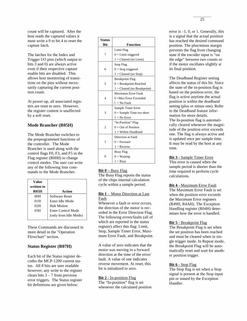
Bit 0 – Busy Flag The Busy Flag reports the status of the chips internal calculation cycle within a sample period. Bit 1 - Motor Direction at Last Fault Whenever a fault or error occurs, the direction of the motor is rec-orded in the Error Direction Flag. The following errors/faults (all of which are reported in the status register) affect this flag: Limit, Stop, Sample Timer Error, Maxi-mum Error Fault, and Breakpoint. A value of zero indicates that the motor was moving in a forward direction at the time of the error/ fault. A value of one indicates reverse movement. At reset, this bit is initialized to zero. Bit 2 - In-position Flag The “In-position” flag is set whenever the calculated position
error is –1, 0, or 1. Generally, this is a signal that the actual position has reached the desired command position. The plus/minus margin prevents the flag from changing state if the encoder input is “on the edge” between two counts or if the motor oscillates slightly at its final position. The Deadband Register setting affects the status of this bit. Since the state of the in-position flag is based on the position error, the flag is active anytime the actual position is within the deadband setting (plus or minus one). Refer to the Deadband feature infor-mation for more details. The In-position flag is automati-cally cleared whenever the magni-tude of the position error exceeds one. The flag is always active and is updated once per sample time. It may be read by the host at any time. Bit 3 - Sample Timer Error This error is caused when the sample period is shorter than the time required to perform cycle calculations. Bit 4 - Maximum Error Fault The Maximum Error Fault is set when the position error exceeds the Maximum Error registers (R49H, R4AH). The Exception Handling register (R04H) deter-mines how the error is handled. Bit 5 - Breakpoint Flag The Breakpoint Flag is set when the set position has been reached and must be cleared when in sin-gle trigger mode. In Repeat mode, the Breakpoint Flag will be auto-matically reset and wait for anoth-er position trigger. Bit 6 - Stop Flag The Stop flag is set when a Stop signal is present at the Stop input pin or issued by the Exception Handler.
Status Bit
Function
7
Limit Flag 0 = Limit triggered 1 = Cleared (no Limit)
6
Stop Flag 0 = Stop triggered 1 = Cleared (no Stop)
5
Breakpoint Flag 0 = Breakpoint Reached 1 = Cleared (no Breakpoint)
4
Maximum Error Fault 0 =Max Error Exceeded l = No Fault
3
Sample Timer Error 0 = Sample Time too short 1 = No Error
2
“In-Position” Flag 0 = Out of Position 1 = Within Deadband
1
Direction at Fault 0 = Forward 1 = Reverse
0
Busy Flag 0 = Waiting 1 = Busy
26
Bit 7 - Limit Flag The Limit flag is set when a Limit signal is present at the Limit input pin or issued by the Exception Handler. Motor Command Register (R08H) The 12-bit Motor Command Port consists of register R08H as the 8-bit MSB and register R4CH as the 4-bit LSB (4 lower bits of register are ignored). The register is con-nected to external pins MC0-MC11. The registers can be read and written to at anytime; howev-er, they should be written to only in the Idle mode. The Motor Command Port oper-ates in two modes, bipolar and unipolar, when under control of internal software. Bipolar mode allows the full range of values in RO8H (-2048D to +2047D). The data written to the Motor Com-mand Port by the control algo-rithms is the internally computed 2's-complement motor command with an 800H offset added. This allows direct interfacing to a DAC with full voltage swings about zero. Unipolar mode functions such that with the same DAC circuit, the motor command output is restrict-ed to positive values (800H to FFFH) when in a control mode. In Unipolar mode, the user can still write a negative value to the Motor Command registers when in IDLE mode. Unipolar mode or Bipolar mode is programmed by setting or clearing flag F2 in the Flag Register R00H. Internally, the MCP-1200 operates on data of 24, 16 and 8- bit lengths to produce the 12-bit mo-tor command, available externally. Many times the computed motor command will be greater than 12
bits. At this point, the controller saturates the motor command. DAC Saturation Limit (R4BH) Default Value = F0H (Established during soft reset) Host readable/writable at any time When internal calculations create a motor command that exceeds the 8-bit range of the most significant byte of the DAC output, the actual value presented at the DAC pins is limited to the setting in register R4BH. In bipolar mode the most signifi-cant byte of the DAC can range from 00H to FFH. 80H represents zero output (000H-7FFH represent reverse rotation while 801H-FFFH are forward). The saturated value output by the controller is not the full-scale value 000H, or FFFH. The saturated value is adjusted to the saturation limit stored in regis-ter R4BH. The default saturation limit is set to 0F0H (negative satu-ration) and F00H (positive satura-tion). Valid values for R4BH range from 81H to FFH. Values less than 80H represent negative motor commands and are internally complemented. Any positive limit value also results in a negative limit of equal magnitude. For example, a setting of E7H limits the most significant byte of posi-tive motor commands to E7H, but also limits the negative motor command to 18H. The saturation limit is only in ef-fect when the internally calculated motor command exceeds an 8-bit range of the MSB. This means that output values exceeding the register value are possible. De-spite the default limit of F0H, a motor command of FEH, for ex-ample, could be output. Only when the calculated value exceeds
FFH would the output “fold back” to the limit of F0h. DAC Offset (R0AH) Default/Reset Value = 0 Host readable/writable at any time The 8-bit value stored in the DAC Offset register represents a signed (2’s complement) adjustment to the lower 8-bits of the 12-bit DAC output. The purpose of this fea-ture is to compensate for any fixed DC bias in the external Digital-to-Analog amplifier circuitry. The lower four bits (nibble) of DAC Offset are added to the low-er 4 bits of the Motor Command output, while the upper nibble (with sign extension) is added to the most significant byte sent to the DAC. The resolution is one 12-bit DAC count. Note that if an 8-bit DAC is in use, only the up-per 4-bits of DAC Offset will have any effect. The DAC Offset feature is effec-tive at all times and in all modes except when the host writes di-rectly to the DAC registers (in Idle mode). In this case, the host values are applied to the DAC without modification. This is use-ful in determining the proper val-ue for the offset for a particular hardware amplifier. At reset, OFFSET is loaded with zero, effectively disabling this feature. PWM Command Registers (RO9H MSB) (R4DH Fraction) The PWM port outputs the motor command as a pulse width modu-lated signal with the correct sign of polarity. The PWM port con-sists of the Pulse and Sign pins corresponding to the PWM com-mand (R09H) and 4-bit fraction (R4DH) in extended address space.
27
Internal to the chip, motor com-mand calculations always produce a 12-bit, 2’s complement value (with a magnitude resolution of 2048). In Idle mode, the host computer can send commands directly to the PWM command port. The 8 most significant bits (including the sign bit) should be written to the PWM Command Port (R09H) while the least signif-icant 4 bits should be placed in the upper nibble (bits 7-4) of the PWM Fraction RegisterR4DH. The lower 4 bits of this register are ignored. The PWM signal at the Pulse pin has a frequency of External Clock/l00 and the duty cycle is resolved into the 100 clocks. (For example, a 2 MHz clock gives a 20 KHz PWM frequency.) The Sign pin gives the polarity of the command. A low output on the Sign pin is positive polarity. The 2's-complement contents of R09H determine the duty cycle and polarity of the PWM com-mand. For example, D8H (-40D) gives a 40% duty cycle signal at
the Pulse pin and forces the Sign
pin high. Data outside the 64H (+ 100D) to 9CH (- 100D) linear range gives 100% duty cycle. R09H can be read and written to, but the user should only write to R09H when the controller is in the Initialization/Idle mode. The PWM Port Output table be-low shows the PWM output ver-sus the internal motor command. When any Control mode is being executed, the unadjusted internal 2's-complement motor command is written to R09H. Because of the hardware limit on the linear range (64H to 9CH, 100D), the PWM port saturates sooner than the 8- bit Motor Command port (00H to FFH, + 127D to -128D). When the internal motor com-mand saturates above 8 bits, the PWM port is saturated to the full ±100% duty cycle level. Note that
the Unipolar setting does not af-
fect the PWM port. The PWM port has an option that can be used with H-bridge type amplifiers. The option is Sign Reversal Inhibit, which inhibits the Pulse output for one PWM period after a sign polarity rever-sal. This allows one pair of tran-sistors to turn off before others are turned on and thereby avoids a short across the power supply. Bit 6 in the Advanced Configuration register (R02H) controls the Sign Reversal Inhibit option. The Sign Reversal diagrams shown below represent the output of the PWM port when the Sign Reversal In-hibit bit is set (1).
Motor Command, MSB
Hex 80h 9Ch CEh FEh 00h 02h 32h 64h 7Fh
Dec -128 -100 -50 -2 0 2 50 100 127
PWM Duty Cycle 100% 100% 50% 2% 0% 2% 50% 100% 100% PWM with 50% Bias 0% 0% 25% 49% 50% 51% 75% 100% 100%
28
SIGN
PULSE
V
TIME
Sign Reversal Inhibit
00H 19H 32H 48H 64H 7FHE7HCEHB5H9CH80H
25
50
75
100
PWM
SIGN = LOWSIGN = HIGH
Reg 09H Contents
PWM Port Output
29
PWM Resolution (R1AH) R1AH – Encoder Filter Clock / PWM Resolution The PWM (Pulse-Width Modulat-ed) output has a duty cycle that is proportional to the internally cal-culated motor command. While in Idle mode the PWM output may be manually manipulated by writing to the PWM Command Port and PWM Fraction registers. The range the PWM output al-ways extends from 0% duty cycle (low signal) to 100% duty cycle (high signal). However, the fre-quency (or repetition rate) of the output depends on the resolution of the PWM signal. While this resolution is selectable by the us-er, the range of useful values is dependent on the system clock used for the chip. The relationship is governed by the equation: PWM Freq. = Clk Freq/PWM Res The table below summarizes this relationship. Bits 0 through 3 of R1AH are used to control the PWM resolu-tion. Note that the upper 4-bits of this register are used for the quad. encoder filter clock previously discussed in Pin Functionality section. One of nine settings may be used (0-8). Values outside this range (i.e. 9-15) will give the same results as setting 8. The default setting at power-up is 0. In general, the higher the setting the higher the resolution, but the lower the PWM frequency. Very high frequencies can be inefficient due to switching losses within the motor driver hardware. Low fre-quencies can produce irritating audible switching noise. Frequen-cies around 20KHz are generally preferred and are highlighted in the table.
PWM 50% Bias Mode R02H – Advanced Configuration Register
Bit 3 = PWM Bias (0=None, 1=50% Duty Cycle) In normal operation the PWM duty cycle is proportional to the magnitude of the motor command signal. A zero motor command (motor stopped) results in a zero duty cycle (output low). Positive and negative values of equal mag-nitude are represented by outputs with identical duty cycles. The sign of the motor command is carried on a separate pin. If bit 3 of the Advanced Configu-ration Register R02H is set to 1, the PWM output carries both sign and magnitude information. A zero motor command will result in a 50% duty cycle. Motor com-mands for positive movement will have duty cycles ranging from 50+% to 100%, while commands for negative movement (reverse rotation) have duty cycles from 50-% to 0%. This mode is particularly useful when the PWM output is used to monitor the Position Error (for diagnostic purposes). Refer to the example given in the appendix that describes how to configure and use the Diagnostic mode us-
ing the PWM 50% duty cycle out-put. The PWM duty cycle values for various clock and PWM resolu-tions are summarized in the table above. Backlash Compensation (R44H) The Backlash register R44H com-pensates for the amount of back-lash in gears or screw nuts. The amount entered is the number of encoder quadrature counts to compensate and should be entered after the backlash has been taken out by driving the motor in one direction. The compensation is executed whenever the direction changes in any control mode (po-sition, interpolation, profile and velocity). Backlash compensation does not guarantee a level of accu-racy but is useful for reducing the effect of backlash in the system. It’s safer to underestimate the amount of backlash in the system. When backlash is used (non-zero value), the system should verify absolute position periodically to eliminate any accumulated back-lash errors.
Reg. 1AH Bits 3, 2, 1, 0)
PWM Modulation Frequency (kHz) and resulting required Clock Freq. (MHz)
Value Res 2 4 6 8 10 12 16 20 0 100 20.00 40.00 60.00 80.00 100.00 120.00 160.00 200.00 1 150 13.33 26.67 40.00 53.33 66.67 80.00 106.67 133.33 2 200 10.00 20.00 30.00 40.00 50.00 60.00 80.00 100.00 3 300 6.67 13.33 20.00 26.67 33.33 40.00 53.33 66.67 4 400 5.00 10.00 15.00 20.00 25.00 30.00 40.00 50.00 5 600 3.33 6.67 10.00 13.33 16.67 20.00 26.67 33.33 6 800 2.50 5.00 7.50 10.00 12.50 15.00 20.00 25.00 7 1200 1.67 3.33 5.00 6.67 8.33 10.00 13.33 16.67 8 1600 1.25 2.50 3.75 5.00 6.25 7.50 10.00 12.50
PWM Frequency is the repetition rate of each PWM frame. A 50% duty cycle would result in
a square wave at this frequency. Bold values indicate closest to 20 KHz for each clock frequency. "Resolution" refers to the number of discrete steps between 0% and 100% duty cycle.
30
Deadband Register (R45H) The Deadband register R45H holds an 8-bit scalar value repre-senting the number of position counts on each side of the com-mand position for which the motor output is deactivated. For exam-ple, if the command position is 1000 and the deadband is 2, the motor will be deactivated for ac-tual position counts of 998, 999, 1000, 1001, and 1002. The software implements the deadband function by modifying the position error value. The ac-tual position is subtracted from the command position to produce an error value that is passed to the filter function. If the magnitude of the error is less than the deadband value, the error is set to zero. The deadband is active in all posi-tion control modes. A deadband setting of zero causes the Deadband routine to be bypassed. Actual Position Registers Read/Clear: R12H, R13H, R14H Preset: R15H, R16H, R17H The Actual Position Register is accessed by two sets of registers in the MCP-1200. When reading the Actual Position from the MCP-1200, the host processor will read Registers R12H (MSB), R13H, and R14H (LSB). When presetting the Actual Position Register, the processor will write to Registers R15H (MSB), R16H, and R17H (LSB). When reading the Actual Position registers, the order must be R14H, R13H, and R12H. These registers are loaded after reading R14H. All three bytes will be latched so that count data does not change while reading three separate bytes.
When presetting the Actual Posi-tion Register, write to R15H and R16H first. When R17H is writ-ten to, all three bytes are simulta-neously loaded into the Actual Position Register. The Actual Position Registers can be simulta-neously cleared at any time by writing any value to R13H. Note that presetting the actual registers while the MCP-1200 is in Control mode may require set-ting the Command Position regis-ters equal to the new Actual Posi-tion to keep from a run-away condition. It is best to perform this adjustment when the Busy flag is not asserted. It is also con-ceivable that slight adjustments of the Actual Position can be an ef-fective method to perform lead-screw compensation. Actual Velocity Registers R34H – Actual Velocity LSB R35H – Actual Velocity MSB The Actual Velocity registers con-tain a 16-bit, 2’s-complement val-ue equal to the velocity in encoder counts per sample time. Once per sample cycle, the position count of the previous sample cycle (n-1) is subtracted from the current po-sition count (n). The result of the subtraction is placed in the actual velocity registers and is available to the host. Since the result is updated each sample cycle, valid velocity in-formation is available in all modes except Idle mode. To avoid the possibility of reading values while they are being changed by the chip, the host should read the Actual Velocity registers only when the BUSY pin/flag is low. Alternatively, the registers may be read at any time provided that the host tests for the possibility of
reading during a firmware update by using the following sequence: 1. Read the MSB (R35H) 2. Read the LSB(R34H) 3. Read the MSB again. If the
value is not the same as in step 1, repeat the process.
High-Res Velocity Registers R23H – High-Res. Command
Velocity MSB R24H – High-Res. Command
Velocity LSB R25H – High-Res. Command
Velocity FRAC R28H – Maximum Velocity –
Position Profile Mode R3CH – Command Velocity –
Vel. Profile Mode The High-Res Velocity registers are used in all Position and Veloc-ity Profile modes when enabled using bit 5 of the Feature Control Register (R01H). Locations R23H, R24H, and R25H contain the high-resolution velocity com-mand and may replace the 8-bit versions (R28H, R3CH). The Command Velcocity registers form a 24-bit, 2’s-complement command. The LSB (R25H) contains the fraction. Units for the entire 24-bit value are then: quadrature counts per sample time, divided by 256. The power-on default is set to low-resolution, 8-bit compatibility for use with registers R3CH and R28H in velocity and Position profiles, respectively. These 8-bit registers contain no fractional parts and have limited dynamic range. In Summary, select configuration to operate in 8-bit or 24-bit veloci-ty modes by setting bit 5 of the Feature Control Register (R01H). Then use the appropriate Com-mand Velocity for the mode se-lected. Once the Feature Control Register is set for 24-bit Com-mand Velocity, the chip will use
31
the High Resolution Velocity reg-isters (R23H, R24H, R25H) in place of the 8-bit Integral Velocity (R3CH) and Maximum Velocity (R28H) registers. Maximum Error Registers R49H – Maximum Error LSB R4AH – Maximum Error MSB R07H – Status Register
Bit 4 = Max Error Fault Flag R04H – Exception Handling Reg-ister
Bit 7 & Bit 6 = Control Bits for Max Error Faults Once each sample time, the dif-ference between the actual posi-tion and the command position is calculated. The absolute value of this difference (which represents the position error in quadrature counts) is compared to the content of Max Error registers (a 16-bit scalar). If the calculated error exceeds the Max Error value, the active-low max error fault flag (bit 4 of the Status Register) is cleared. This bit will remain cleared until reset by writing any value to the Status Register. The response to the Max Error Fault is determined by the value of bits 7 and 6 in the Exception Handling Register. Responses include: only setting the flag (00), going into Idle mode (01), decel-erating (10), and abruptly stopping (11). Refer to the section on Ex-ception Handling for more details. On reset the Max Error registers are initialized to FFFFH (effec-tively disabling this function). Additionally on reset the Excep-tion Handling bits are loaded with (00), and the Max Error Fault Flag is reset. The Max Error fault is also used during Stepper motor operation. While the flag in the Status regis-ter and the control bits in the Ex-ception Handling Register operate in an identical manor, the error
triggering the fault has a different source. Refer to the Step Encoder Follower section for a detailed description. Lead-lead Filter Registers R20H - Zero (A) R21H - Pole (B) R22H - Gain (K) All servo control modes use one of the programmable digital filters D (z) to compensate for closed loop system stability. The com-pensation D (z) has the form:
)256
(4
)256
()( Bz
AzKzD
+
−= [1]
Where, z = the digital domain operator K = digital filter gain (R22H) A = digital filter zero (R20H) B = digital filter pole (R21H) T = sample time The compensation is a first-order lead filter which in combination with the sample rate affects the dynamic step response and stabil-ity of the control system. All pa-rameters, A, B, K, and T, are 8-bit scalars that can be changed by the user at any time. As shown in equation [2], the digital filter uses previously sam-pled data to calculate D (z). This old internally sampled data is cleared when the Idle mode is executed. The digital filter is implemented in the time domain as shown be-low:
MCn = (K/4)(En)- [(A/256)(K/4)(En-1) + (B/256)(MCn-1)] [2]
where: n = current sample time n-l = previous sample time MCn = Motor Command Output at n MCn-l = Motor Command Output at n-1 En = Position Error at n Xn-l = Position Error at n-l PID Filter Registers R61H – Kp Proportional Gain Factor (KP) R62H – Ki Integral Gain Factor (KI) R63H – Kd Derivative Gain Factor (KD) R64H – Derivative Span Code (K) R66H & R65H – Integral Limit MSB & LSB (ILIM) R69H – Ka Acceleration Feed-forward Gain Factor (KA) R6AH – Kv Velocity Feed-forward Gain Factor (KV) Setting bit 3 of the Feature Con-trol register R01H enables the PID filter. Each sample period, the difference between the command position and the actual position (the position error) is input to the filter routine. The routine then computes the motor command using the following equations: MCn = Pterm + Iterm + Dterm + Vterm + Aterm (See Scaling Note Below)
Pterm = Kp * PEn Iterm = Ki * IACCn IACCn = IACCn-1 + PEn If MCn-1 is saturated then IACCn = IACCn-1 If IACCn > ILIM then IACCn = ILIM If IACCn < -ILIM then IACCn = -ILIM Dterm = Kd * (PEn - PEn-k) Vterm = Kv * CmdVel Aterm = Ka * CmdAcc
Where:
32
MCn = Motor Command Kp, Ki, Kd = Gain values for each term PEn = Position Error (Cmnd. Pos. - Act. Pos.) for this sample cycle IACCn = Integral Accumulator ILIM = Integrator Maximum magnitude PEn-k = PE ‘k’ sample times ago K = Derivative Span (in sample cycles) Legal values for K are 1, 2, 3, and 4 (default 1) If an illegal value is entered, the default value is used CmdVel = Command Velocity = CmndPosn – CmndPosn-1 CmdAcc = Command Accelera-tion = CmdVeln – CmdVeln-1 The subscript “n-1” indicates a value from the previous sample time.
Scaling:
To provide sufficient range and sensitivity, while permitting the use of 8-bit gain factors, the terms of the motor command equation are internally scaled as follows: MC = (Pterm/32 + Iterm/8192 + Dterm/8 + Vterm/16 + Aterm Feed-forward Compensation:
The velocity and acceleration feed-forward terms (Vterm and Aterm) require current command velocity and acceleration infor-mation. In the Profile, Integral Velocity, and Interpolation Modes this data is internally calculated for the PID routine. However, if the host computer generates moves by sending new command positions every sample period while in Position Control mode, these values are not created inter-nally. If the user wishes to use feed-forward compensation in Position Control mode, he must provide current velocity information. The velocity, in quadrature counts per
sample period / 256, should be written to the Command Feed-forward Velocity Registers (R57H and R56H). The format for this data is a 2’s complement 16-bit value [8.8] with 8 bits of integer (R57H) and 8 bits of fraction (R56H). If the value exceeds the range of these registers, the max-imum allowable value should be entered (i.e. 8001h or 7FFFh). The command acceleration is in-ternally created from the velocity values and is not entered by the user. In most cases the user should con-sider using the Interpolated Posi-tion or Interpolated Velocity modes for this type of movement which allows feed-forward com-pensation without host entry of velocity. Sample Timer (R0FH) R10H – Sample Timer Prescalar MSB Register R11H – Sample Timer Prescalar LSB Register The sampling period of the chip is controlled by two count-down timers. The first, a 16-bit prescalar, takes the system clock and effectively divides it by the value of the Sample Timer Prescalar Registers (R10H & R11H) plus one. The output of this prescalar is then used as the clock for a second, 8-bit, timer. This timer counts down to zero, then reloads the value contained in the Sample Timer Register (R0FH) and counts down again. Each time zero is reached a signal is produced that synchronizes the firmware sample cycle. The equation for the relationship between the sample time and these timers is as follows: Sample Time = ((Prescalar MSB*256 + Prescalar LSB)+1) * (Timer +1) * 1/Clk Freq.
Where: Prescalar MSB = Value of Sample Timer Prescalar Register (R10H) Prescalar LSB = Value of Sample Timer Prescalar Register (R11H) Sample Timer = Value of Sample Timer Register (R0FH) At power-up, R0FH = 40H, R10H = 0, and R11H = 3FH. With an 8 MHz clock, this results in a de-fault sample time of: (63+1)*(64+1)*(1/8,000,000) = 520 µS. This default value provides the internal processor ample time to execute all combinations of modes and features. At higher system clock rates the minimum sample time is proportionately shorter. For example, at 20MHz the de-fault sample period is 208 µS. Since most mechanical systems benefit little from sample periods shorter than 500 µS, the user should increase the prescalar and/or timer values to achieve a reasonable sample time. If the sample period is too short to allow sufficient time for the internal processor to complete all tasks, an error will be generated and the system will return to Idle mode. Refer to the Sample Timer Error section for details. Reading the value of R10H and R11H will reveal the prescalar setting. However, reading R0FH will show the current value of the sample timer count. This value can range from the timer reload value (the value written to R0FH) down to zero. Reading R0FH provides an indication of the cur-rent point in the sample cycle. The following table details Prescalar Register values for a number of system clock rates. For simplicity, the Sample Timer Reg-ister is held constant. However, the sample timer could be varied
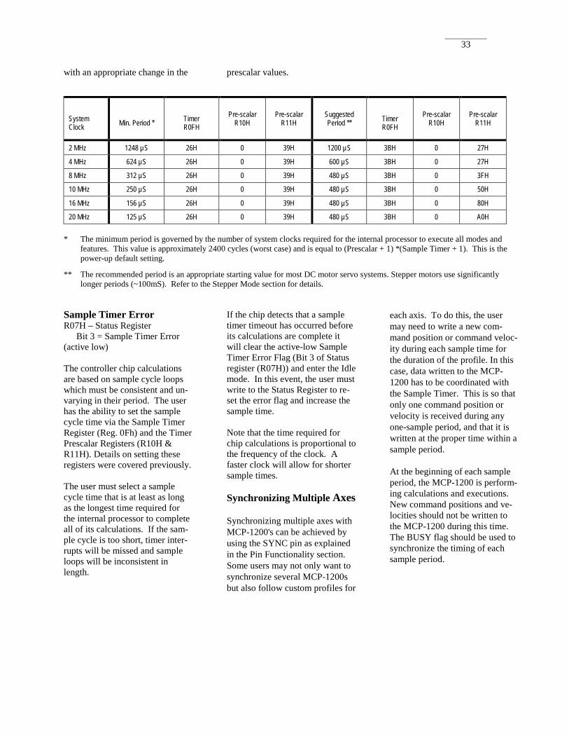
33
with an appropriate change in the prescalar values.
* The minimum period is governed by the number of system clocks required for the internal processor to execute all modes and features. This value is approximately 2400 cycles (worst case) and is equal to (Prescalar + 1) *(Sample Timer + 1). This is the power-up default setting.
** The recommended period is an appropriate starting value for most DC motor servo systems. Stepper motors use significantly
longer periods (~100mS). Refer to the Stepper Mode section for details. Sample Timer Error R07H – Status Register
Bit 3 = Sample Timer Error (active low) The controller chip calculations are based on sample cycle loops which must be consistent and un-varying in their period. The user has the ability to set the sample cycle time via the Sample Timer Register (Reg. 0Fh) and the Timer Prescalar Registers (R10H & R11H). Details on setting these registers were covered previously. The user must select a sample cycle time that is at least as long as the longest time required for the internal processor to complete all of its calculations. If the sam-ple cycle is too short, timer inter-rupts will be missed and sample loops will be inconsistent in length.
If the chip detects that a sample timer timeout has occurred before its calculations are complete it will clear the active-low Sample Timer Error Flag (Bit 3 of Status register (R07H)) and enter the Idle mode. In this event, the user must write to the Status Register to re-set the error flag and increase the sample time. Note that the time required for chip calculations is proportional to the frequency of the clock. A faster clock will allow for shorter sample times. Synchronizing Multiple Axes Synchronizing multiple axes with MCP-1200's can be achieved by using the SYNC pin as explained in the Pin Functionality section. Some users may not only want to synchronize several MCP-1200s but also follow custom profiles for
each axis. To do this, the user may need to write a new com-mand position or command veloc-ity during each sample time for the duration of the profile. In this case, data written to the MCP-1200 has to be coordinated with the Sample Timer. This is so that only one command position or velocity is received during any one-sample period, and that it is written at the proper time within a sample period. At the beginning of each sample period, the MCP-1200 is perform-ing calculations and executions. New command positions and ve-locities should not be written to the MCP-1200 during this time. The BUSY flag should be used to synchronize the timing of each sample period.
System Clock
Min. Period *
Timer R0FH
Pre-scalar R10H
Pre-scalar R11H
Suggested Period **
Timer R0FH
Pre-scalar R10H
Pre-scalar R11H
2 MHz 1248 µS 26H 0 39H 1200 µS 3BH 0 27H
4 MHz 624 µS 26H 0 39H 600 µS 3BH 0 27H
8 MHz 312 µS 26H 0 39H 480 µS 3BH 0 3FH
10 MHz 250 µS 26H 0 39H 480 µS 3BH 0 50H
16 MHz 156 µS 26H 0 39H 480 µS 3BH 0 80H
20 MHz 125 µS 26H 0 39H 480 µS 3BH 0 A0H
34
Operation Flowchart The MCP-1200 executes any one of two setup routines and five control modes selected by the user. The two setup routines are Reset and Idle. The setup routines may be entered using the Program Counter (R05H). Reset can also be entered by triggering the Reset pin or internally generated by the Exception Handler. The five control modes available to the user include: Position Control Profile Generation Position Interpolation Velocity Interpolation Integral Velocity
The MCP-1200 switches from one control mode to another as a result of the user setting flags F0, F3, F4 or F5 in the Flag register (R00H). This next section describes the function of each setup routine and control mode and the initial condi-tions which must be provided by the user to switch from one mode to another. The MCP-1200 Flowchart shows the setup rou-tines and control modes, and shows the commands required to switch from one mode to another.
Reset/Init
Idle Mode
Mode Brancher (R05H)
Reset (0)?
Idle (1)?
Control (>2)? NO
YES
YES
YES
Error/Exception Handler
Breakpoint Routine
Test Flag Register (00H)
Trapezoidal or S-Curve Profile Generator
Profile (F0 =1)?
Vel. Interp. (F4 =1)?
Pos. Interp. (F3 =1)?
Integral Vel. (F5 =1)?
Position Interpolation
Velocity Interpolation
Velocity Interpolation
Command Pos Inc. (R0BH)
Sample Timer (R0FH) = 0?
NO
Update Actual Vel. & Pos. Backlash Correction (≠ 0)
Calc. Pos. Error Deadband Compensation (≠ 0)
Lead Filter PID Filter
Stepper Motor Mode?
Stepper Motor Mode?
Calc. Steps/Sample
Pulse & Direction Outputs
PWM & DAC Outputs
Reset Pin (Low)
35
Setup Modes Hard Reset Executed by: -Pulling the RESET pin low (re-quired at power up) When a hard reset is executed (RESET pin goes low), the fol-lowing conditions occur: -All output signal pins are held low except Sign, Data bus, and Motor Command.
-All flags (F0 to F5) are cleared. The Pulse pin of PWM port is set low while the Reset pin is held low. After the Reset pin is released (goes high) the Pulse pin goes high for one cycle of the external clock driving the MCP-1200. The Pulse pin then returns to a low output. -The Motor Command port (R08H) is preset to 80H (128D). -The Commutator logic is cleared. -The I/O control logic is cleared. -A soft reset is automatically exe-cuted. Soft Reset Executed by: -Writing 00H to R05H, or -Automatically called after a Hard reset When a soft reset is executed, the following conditions occur: -The digital filter parameters are preset to A (R20H) = E5H (229D) B (R21H) = K (R22H) = 40H (64D) -The Sample Timer (R0FH) is
preset to 40H (64D). -The Status register (R07H) is
cleared. -The Actual Position Counters (R12H, R13H, and R14H) are cleared to 0. From Reset mode, the MCP-1200 goes automatically to Initialization/Idle mode.
Idle Mode Executed by: -Writing 0lH to R05H, or -Automatically executed after a hard
reset, soft reset, or -Limit pin goes low. The Initialization/Idle mode is entered either automatically from Reset; by writing l to the Program Counter (R05H) under any condi-tions, or pulling the Limit pin low. In the lnitialization/ldle mode, the following occur: -The lnitialization/ldle flag (FI) is set. -The PWM port R09H is set to 00H (zero command). -The Motor Command port (RO8H) is set to 80H (128D) (ze-ro command). -Previously sampled data stored in the digital filter is cleared. It is at this point that the user should pre-program all the neces-sary registers needed to execute the desired control mode. The MCP-1200 stays in this mode (idling) until a new mode com-mand is given.
36
Control Modes Control flags F0, F3, and F5 in the Flag register (R00H) determine which control mode is executed. Only one control flag can be set at a time. After one of these control flags is set, the control modes are entered from the Initialization/Idle mode by writing 03H to the Pro-gram Counter (R05H). Position Control Mode Flags: F0 Cleared F3 Cleared F5 Cleared Registers Used: R0CH - Command Pos. MSB R0DH - Command Pos. CSB R0EH - Command Pos. LSB R0BH – Command Pos. Incr. Position Control performs point- to-point position moves with no velocity profiling. The user speci-fies a 24-bit position command, which the controller compares to the 24-bit actual position. The
position registers are formatted as two’s complement values. The position error is calculated from the command and actual positions, the full digital compensation is applied and the motor command is output to the command ports. Position is measured in encoder quadrature counts. The command position resides in R0CH (MSB), R0DH, and R0EH (LSB). Writing to R0EH latches all 24 bits at once for the control algorithm. Therefore, the com-mand position is written in the sequence R0CH, R0DH and R0EH. The command registers can be read in any desired order. The actual position resides in R12H (MSB), R13H, and R14H (LSB). Reading R14H latches the upper two bytes into an internal buffer. Therefore, Actual Position registers are read in the order of R14H, R13H, and R12H for cor-rect instantaneous position data.
The 8-bit, 2’s complement value in the Command Position Adder register (R0BH) is added to the Command Position. This feature is only available in Position Con-trol mode. By using this feature the position can be changed with-out having to write the full 24-bit Command Position registers. The value in register R0BH is checked each sample period. If it is not zero, the value is added to the Command Position registers. Register R0BH is then loaded with zero. Note that each move is limited to -128 to 127 encoder counts. However, by monitoring the busy line the Command Posi-tion Adder may be updated each sample time. This feature is use-ful for generating custom user defined profiles. Upon reset the Command Position Adder is initialized to zero. Load-ing any non-zero value into the register will activate this feature.
Example Code to Program position Moves (Begin) Hard Rest (MCP-1200 goes into INIT/IDLE Mode)
Initialize Filter, Timer, Command Position Registers Write 03H to Register R05H
(MCP-1200 is now in Position Mode) Write Desired Command Position to Command Position Registers (Controller Moves to new position) Continue writing in new Command Positions (End) Integral Velocity Mode Flags: F0 Cleared F3 Cleared F5 Set to begin move Registers Used: R00H - Flag Register R26H - Acceleration LSB R27H - Acceleration MSB
R3CH – Command Vel (8-bit mode) R23H – Command Vel (MSB) R24H – Command Vel (MID) R25H – Command Vel fraction (LSB) Integral Velocity Control per-forms continuous velocity profil-ing which is specified by com-mand velocity and command
acceleration. Integral Velocity is specified as either 8-bit or 24-bit by setting bit 5 of the Feature Control Register (R01H). The user can change velocity and acceleration any time to continu-ously profile velocity in time. Once the specified velocity is
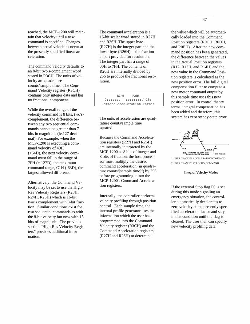
37
reached, the MCP-1200 will main-tain that velocity until a new command is specified. Changes between actual velocities occur at the presently specified linear ac-celeration. The command velocity defaults to an 8-bit two's-complement word stored in R3CH. The units of ve-locity are quadrature counts/sample time. The Com-mand Velocity register (R3CH) contains only integer data and has no fractional component. While the overall range of the velocity command is 8 bits, two's- complement, the difference be-tween any two sequential com-mands cannot be greater than 7 bits in magnitude (ie.127 deci-mal). For example, when the MCP-1200 is executing a com-mand velocity of 40H (+64D), the next velocity com-mand must fall in the range of 7FH (+ 127D), the maximum command range, C1H (-63D), the largest allowed difference. Alternatively, the Command Ve-locity may be set to use the High- Res Velocity Registers (R23H, R24H, R25H) which is 16-bit, two’s complement with 8-bit frac-tion. Similar conditions exist for two sequential commands as with the 8-bit velocity but now with 15 bits of magnitude. The previous section “High-Res Velocity Regis-ters” provides additional infor-mation.
The command acceleration is a 16-bit scalar word stored in R27H and R26H. The upper byte (R27H) is the integer part and the lower byte (R26H) is the fraction-al part provided for resolution. The integer part has a range of 00H to 7FH. The contents of R26H are internally divided by 256 to produce the fractional reso-lution.
R27H R26H 0IIIIIII FFFFFFFF/ 256
Command Acceleration Format The units of acceleration are quad-rature counts/sample time squared. Because the Command Accelera-tion registers (R27H and R26H) are internally interpreted by the MCP-1200 as 8 bits of integer and 8 bits of fraction, the host proces-sor must multiply the desired command acceleration (in quadra-ture counts/[sample time]2) by 256 before programming it into the MCP-1200's Command Accelera-tion registers. Internally, the controller performs velocity profiling through position control. Each sample time, the internal profile generator uses the information which the user has programmed into the Command Velocity register (R3CH) and the Command Acceleration registers (R27H and R26H) to determine
the value which will be automati-cally loaded into the Command Position registers (R0CH, R0DH, and R0EH). After the new com-mand position has been generated, the difference between the values in the Actual Position registers (R12, R13H, and R14H) and the new value in the Command Posi-tion registers is calculated as the new position error. The full digital compensation filter to compute a new motor command output by this sample time uses this new position error. In control theory terms, integral compensation has been added and therefore, this system has zero steady-state error.
1: USER CHANGES ACCELERATION COMMAND
2: USER CHANGES VELOCITY COMMAND
Integral Velocity Modes If the external Stop flag F6 is set during this mode signaling an emergency situation, the control-ler automatically decelerates to zero velocity at the presently spec-ified acceleration factor and stays in this condition until the flag is cleared. The user then can specify new velocity profiling data.
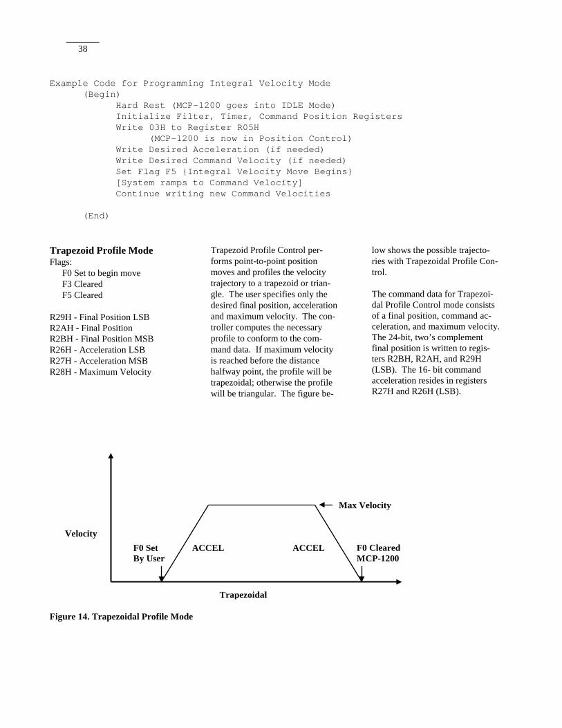
38
Example Code for Programming Integral Velocity Mode (Begin) Hard Rest (MCP-1200 goes into IDLE Mode)
Initialize Filter, Timer, Command Position Registers Write 03H to Register R05H
(MCP-1200 is now in Position Control) Write Desired Acceleration (if needed) Write Desired Command Velocity (if needed) Set Flag F5 {Integral Velocity Move Begins} [System ramps to Command Velocity] Continue writing new Command Velocities (End) Trapezoid Profile Mode Flags:
F0 Set to begin move F3 Cleared F5 Cleared
R29H - Final Position LSB R2AH - Final Position R2BH - Final Position MSB R26H - Acceleration LSB R27H - Acceleration MSB R28H - Maximum Velocity
Trapezoid Profile Control per-forms point-to-point position moves and profiles the velocity trajectory to a trapezoid or trian-gle. The user specifies only the desired final position, acceleration and maximum velocity. The con-troller computes the necessary profile to conform to the com-mand data. If maximum velocity is reached before the distance halfway point, the profile will be trapezoidal; otherwise the profile will be triangular. The figure be-
low shows the possible trajecto-ries with Trapezoidal Profile Con-trol. The command data for Trapezoi-dal Profile Control mode consists of a final position, command ac-celeration, and maximum velocity. The 24-bit, two’s complement final position is written to regis-ters R2BH, R2AH, and R29H (LSB). The 16- bit command acceleration resides in registers R27H and R26H (LSB).
ACCEL ACCEL F0 Cleared MCP-1200
F0 Set By User
Velocity
Trapezoidal
Max Velocity
Figure 14. Trapezoidal Profile Mode
39
The command acceleration has the same integer and fraction format as discussed in the Integral Veloc-ity Control mode section. The 7-bit Maximum Velocity is a scalar value with the range of 00H to 7FH (0D to 127D). The Maximum Velocity has the units of quadrature counts per sample time, and resides in register R28H. The command data registers may be read or writ-ten to in any order. The internal profile generator pro-duces a position profile using the present Command Position (R0CH-R0EH) as the starting point and the Final Position (R2BH-R29H) as the end point. Once the desired data is entered, the user sets flag F0 in the Flag register (R00H) to commence motion (if the MCP-1200 is al-ready in Control mode).
When the profile generator sends the last position command to the Command Position registers to complete the trapezoidal move, the controller clears flag F0. The MCP-1200 then automatically goes back into Control mode with the final position of the trapezoi-dal move as the Command Posi-tion. When the MCP-1200 clears flag F0 it does NOT indicate that the motor and encoder are at the final position NOR that the motor and encoder have stopped. The flag indicates that the command profile has finished and may be moni-tored in the Flag register (R00H) as well at the PROF pin at any time. The motor encoder's true position can only be determined by reading the Actual Position registers. The In-position flag may also be monitored in the Sta-tus register (R07H bit 2) to indi-cate that the move has completed.
Each sample time, the internal profile generator uses the infor-mation which the user has pro-grammed into the Maximum Ve-locity register (R28H), the Command Acceleration registers (R27H and R26H), and the Final Position registers (R2BH, R2AH, and R29H) to determine the value which will be automatically load-ed into the Command Position registers (R0EH, R0DH, and R0CH). After the new command position has been generated, the difference between the value in the Actual Position registers (R12H, R13H, and R14H) and the new value in the Command Posi-tion registers is calculated as the new position error. This new posi-tion error is used by the full digital compensation filter to compute a new motor command output for the sample time. (The register block diagram in Figure 3 further shows how the internal profile generator works in Trapezoidal Profile mode).
Example Code for Programming Trapezoid Moves {Begin} Hard Reset {MCP-1200 goes into INIT/IDLE Mode} Initialize Filter, Timer, Command Position Registers Write 03H to Register R05H {MCP-l200 is now in Position Control} {Profile #1} Write Desired Acceleration Write Desired Maximum Velocity Write Final Position Set Flag FO {Trapezoid Move Begins, PROF pin goes high} Poll PROF pin until it goes low (Move is complete) {Profile #2} Write Desired Acceleration Write Desired Maximum Velocity Write Final position Set Flag FO {Trapezoid Move Begins, PROF pin goes high} Poll PROF pin until it goes low (Move is complete) {Repeat} .
40
. . {end} S-Curve Profile R01H – “Feature Control Regis-ter”
Bit 5 – High Resolution Ve-locity (0 = 8bit, 1 = 24bit) Bit 4 – Profile Select (0=Trapezoid, 1=S-Curve)
R23H – “Command Velocity MSB” R24H – “Command Velocity Mid” R25H – “Command Velocity LSB (fraction)” R28H – “Maximum Velocity – Profile Mode” R26H – “Acceleration Factor LSB (fraction)” R27H – “Acceleration Factor MSB” R54H – “Jerk (sub-fraction)” R55H – “Jerk (fraction)” R29H – “Final Position LSB” R2AH – “Final Position Mid” R2BH – “Final Position MSB” The S-curve profile feature is sim-ilar to the Trapezoid profile mode in that the chip calculates a trajec-tory from the present position to a final position. In the trapezoid case velocity and acceleration are controlled. The s-curve feature also controls velocity and acceler-ation, but adds control over jerk. While velocity is defined as the rate of change in position, and acceleration is defined as the rate of change of velocity, jerk is de-fined as the rate of change of ac-celeration. Large values of jerk will create profiles that are identi-cal to those of the trapezoid mode with abrupt changes from acceler-ation to constant velocity move-ment (the “corners” of the trape-zoid). Small values of jerk effectively round off these cor-ners, producing smoother move-ment.
The final position and acceleration parameters use the same registers as in Trapezoidal Profile. The acceleration parameter can be thought of as a maximum acceler-ation value. It is expressed in 2 bytes with one byte representing a fractional value [8.8]. The velocity parameter can be entered in two ways. In the de-fault (compatibility) mode (R01H, bit 5 = 0), the single byte Max Velocity (R40H) register is used [8.0]. In high-resolution velocity mode (R01H, bit2 = 1), the three-byte Command Velocity is used – having 8 fractional bits [16.8]. Refer to the write up on the veloc-ity registers for more information. Jerk is a 16-bit parameter, in which all bits are fractional [0.16] (the maximum value is just under one). Two register locations hold this value (R55H) and (R54H). Bit 4 of the Feature Control Reg-ister (R01H) selects between the trapezoid and S-curve profiles (0=default=trapezoid). Using the S-Curve Feature • Set bit 4 of Feature Control
register to select the S-curve profile.
• From control mode, the user should set the final position, velocity, acceleration, and jerk values.
• Set the profile flag (F0) to start the operation (just as with the trapezoid mode).
The profile flag will be reset by the chip when the profile has completed (identical to the trape-zoid mode).
Modifying a Trapezoid or S-curve Profile Additional Registers: R06H – “Profile Phase Status” R33H – “Accel. Delta Position MSB” R32H – “Accel. Delta Position CSB” R31H – “Accel. Delta Position LSB” The length of a trapezoidal or s-curve profile can be adjusted while the move is in progress – provided that a few conditions are met. While computing the profile the chip passes through a number of operational phases. Most moves pass through seven phases. Dur-ing phases 1, 2, and 3 the motor is accelerating. Phase 4 indicates the steady-state slewing at maxi-mum velocity. Phases 5, 6, and 7 are the deceleration phases. A phase value of 0 indicates that the move has not yet started or that the profile is complete. In cases where maximum values of jerk, acceleration, and/or velocity can-not be reached, some of the seven phases are skipped. In the case of a Trapezoidal profile, Phase 1,3 and Phases 5, 7 may not be de-tected. The current phase is avail-able to the host computer by read-ing the Profile Phase Status (R06H). The user may extend a trapezoidal or S-curve profile move at any time after phase 1 starts and be-fore deceleration starts (phase 5, 6, or 7) by simply writing new values to the Final Position Regis-ters. In practice, the host system
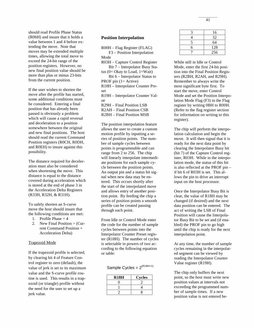
41
should read Profile Phase Status (R06H) and insure that it holds a value between 1 and 4 before ex-tending the move. Note that moves may be extended multiple times, allowing the total move to exceed the 24-bit range of the position registers. However, no new final position value should be more than plus or minus 23-bits from the current position. If the user wishes to shorten the move after the profile has started, some additional conditions must be considered. Entering a final position that has already been passed is obviously a problem which will cause a rapid reversal and deceleration to a position somewhere between the original and new final positions. The host should read the current Command Position registers (R0CH, R0DH, and R0EH) to insure against this possibility. The distance required for deceler-ation must also be considered when shortening the move. This distance is equal to the distance covered during acceleration which is stored at the end of phase 3 in the Acceleration Delta Registers (R33H, R32H, & R31H). To safely shorten an S-curve move the host should insure that the following conditions are met:
1. Profile Phase = 4 2. New Final Position > (Cur-
rent Command Position + Acceleration Delta)
Trapezoid Mode If the trapezoid profile is selected, by clearing bit 4 of Feature Con-trol register to zero (default), the value of jerk is set to its maximum value and the S-curve profile rou-tine is used. This results in a trap-ezoid (or triangle) profile without the need for the user to set up a jerk value.
Position Interpolation R00H – Flag Register (FLAG)
F3 – Position Interpolation Mode R03H – Capture Control Register
Bit 7 – Interpolator Busy Sta-tus (0= Okay to Load, 1=Wait)
Bit 6 – Interpolator Status to PROF pin (1= Active) R18H – Interpolator Counter Pre-set R19H – Interpolator Counter Val-ue R29H – Final Position LSB R2AH – Final Position CSB R2BH – Final Position MSB The position interpolation feature allows the user to create a custom motion profile by inputting a se-ries of position points. The num-ber of sample cycles between points is programmable and can range from 2 to 256. The chip will linearly interpolate intermedi-ate positions for each sample cy-cle between the position points. An output pin and a status bit sig-nal when new data may be en-tered. This occurs shortly after the start of the interpolated move and allows entry of another posi-tion point. By feeding the chip a series of position points a smooth profile can be created passing through each point. From Idle or Control Mode enter the code for the number of sample cycles between points into the Interpolator Counter Preset regis-ter (R18H). The number of cycles is selectable in powers of two ac-cording to the following equation or table:
Sample Cycles = 2(R18H+1)
R18H Cycles 0 2 1 4 2 8
3 16 4 32 5 64 6 128 7 256
While still in Idle or Control Mode, enter the first 24-bit posi-tion into the Final Position Regis-ters (R2BH, R2AH, and R29H). Remember to always write the most significant byte first. To start the move, enter Control Mode and set the Position Interpo-lation Mode Flag (F3) in the Flag register by writing 0BH to R00H. (Refer to the flag register section for information on writing to this register). The chip will perform the interpo-lation calculation and begin the move. It will then signal that it is ready for the next data point by clearing the Interpolator Busy bit (bit 7) of the Capture Control reg-ister, R03H. While in the interpo-lation mode, the status of this bit is also reflected at the PROF pin – if bit 6 of R03H is set. This al-lows the pin to drive an interrupt input on the host processor. Once the Interpolator Busy Bit is clear, the value of R18H may be changed (if desired) and the next data position can be entered. The act of writing the LSB of Final Position will cause the Interpola-tor Busy Bit to be set and (if ena-bled) the PROF pin to go high until the chip is ready for the next interpolation point. At any time, the number of sample cycles remaining in the interpolat-ed segment can be viewed by reading the Interpolator Counter Value register (R19H). The chip only buffers the next point, so the host must write new position values at intervals not exceeding the programmed num-ber of sample times. If a new position value is not entered be-
42
fore the Interpolator Counter reaches zero, the current value in the Final Position registers will be used again. The motor will stop at this position until a new position is entered. To exit the Position Interpolation Mode, clear the F3 flag by writing a 03H to the FLAG register. Velocity Interpolation R00H – Flag Register (FLAG)
F4 – Velocity Interpolation Mode
R03H – Capture Control Register Bit 7 – Interpolator Busy Sta-tus (0= Okay to Load, 1=Wait) Bit 6 – Interpolator Status to PROF pin (1= Active)
R18H – Interpolator Counter Pre-set R19H – Interpolator Counter Val-ue R23H – Command Velocity MSB R24H – Command Velocity CSB R25H – Command Velocity LSB (fraction) The velocity interpolation feature allows the user to create a custom motion profile by inputting a se-ries of velocity values. The num-ber of sample cycles between ve-locity levels is programmable and can range from 2 to 256. The chip will linearly interpolate intermedi-ate velocities for each sample cy-cle between the velocity levels. An output pin and a status bit sig-nal when new data may be en-tered. This occurs shortly after the start of the interpolated move and allows entry of another ve-locity level. By feeding the chip a series of velocities, a smooth pro-file can be created passing through each velocity. From Idle or Control Mode enter the code for the number of sample cycles between velocity levels into the Interpolator Counter Pre-set register (R18H). The number of cycles is selectable in powers
of two according to the table in the previous section. While still in Idle or Control Mode, enter the first 24-bit veloci-ty into the Command Velocity Registers (R23H, R24H, & R25H). R23H and R24H repre-sent integer values while R25H represents a fractional value [16.8]. As a whole, the command velocity is a 24-bit, 2’s comple-ment number (negative values represent reverse rotation) equal to the velocity times 256. Re-member to always write the most significant byte (R23H) first. To start the move, enter Control Mode and set the Velocity Inter-polation Mode Flag (F4) in the Flag register by writing 0Ch to R00H. (Refer to the flag register section for information on writing to this register). The chip will perform the interpo-lation calculation and begin the move. It will then signal that it is ready for the next data point by clearing the Interpolator Busy bit (bit 7) of the Capture Control reg-ister. While in the interpolation mode, the status of this bit is also reflected at the In-motion pin – if bit 6 of Capture Control register is set. This allows the pin to drive an interrupt input on the host pro-cessor. Once the Interpolator Busy Bit is clear, the value of the Interpolator Counter may be changed (if de-sired) and the next data position can be entered. The act of writ-ing the LSB of Command Veloci-ty will cause the Interpolator Busy Bit to be set and the PROF pin to go high until the chip is ready for the next value. At any time, the number of sample cycles remaining in the interpolat-ed segment can be viewed by reading the Interpolator Counter Value register (R19H).
The chip only buffers the next value, so the host must write new velocity values at intervals not exceeding the programmed num-ber of sample times. If a new velocity value is not entered be-fore the Interpolator Count reach-es zero, the current value in the Command Velocity will be used again. The motor will continue running at this velocity until a new velocity is entered. To exit the Velocity Interpolation Mode, clear the F4 flag by writing a 04H to the Flag register.
43
Stepper Motor Control Stepper Control Mode R02H – “Advanced Configuration Register”
Bit 1 – Step Mode Enable (1 = Step Mode On)
Bit 2 – Step Output Polarity (0=High Pulse, 1=Low Pulse) R0FH – “Sample Timer” R10H – “Sample Timer Prescaler MSB” R11H – “Sample Timer Prescaler LSB” R1BH – “Step Pulse Width” (de-fault=15) This mode reconfigures the output to the Pulse and Sign pins (pins 18 and 19) to provide Step and Direc-tion signals for a stepper motor driver. Bit 1 of the Advanced Configuration Register (R02H) is set to one to enable Stepper Motor control. The step pulse polarity and width are programmable. Bit 2 of Ad-vance Configuration register se-lects a high pulse if zero (default) or a low pulse if set to one. The width of the step pulse is depend-ent on the value of the Step Pulse Width Register (R1BH). The re-sulting step pulse is equal to the number of system clock periods specified by the register value plus one: Step Pulse Width = (Register Val-ue + 1) * 1/Clock Freq. For example, the default register value of 15 and a system clock rate of 8 MHz will result in a step pulse width of 2 µS. At 20 MHz, a value of 150 would give the pulse width of 8 µS. To insure adequate set-up time, any change in the direction output precedes the step pulse by a fixed, firmware-determined period of approximately 1080 system clock cycles. At 20 MHz this equates to 54µS.
While the most obvious character-istic of operation in the step mode is the output of Step and Direction signals, the “open-loop” nature of stepper motor operation results in several internal changes in the chip. Although a position encoder may be used as an option to detect motor stalls or driver problems (see the separate Stepper Encoder write-up), position feedback is not required in step mode. As a re-sult, the PID and Lead filters are not used. The step and direction output is feed directly into the position counter. This allows most of the chip’s features to function without modification in the step mode. In the step mode care must be taken in the programming of the sample period in order to insure reasonable values for the velocity and acceleration settings. Details on setting the 16-bit sample timer prescaler and the 8-bit sample timer are covered in a separate section. Specific applications to the step mode are covered here. The combination of prescalar, timer, and speed values result in a tremendous dynamic range for the step rate. With a 20 MHz system clock the maximum rate is 1.28 million steps per second, while the minimum step rate is approxi-mately one step every 3.6 minutes. (These limits scale linearly with clock rate.) The maximum practi-cal step rate is generally limited by the stepper motor, its driver, and the mechanical system being driven. As an example, consider a typical step motor system (bipolar, half-step drive) with a limit of 2500 step pulses per second. Beyond this rate the motor’s rotor is una-ble to reach the next step position in a single pulse period and the motor will stall. To achieve a comfortable range of speed values
it is desirable to have this maxi-mum speed coincide with a ve-locity value toward the upper limit of an 8-bit byte. In this example, choosing a sample rate that would result in 2500 steps per second at a velocity setting of 250 steps per sample cycle would be ideal. 250 steps per sample cycle / 2500 steps per second = 0.1 seconds per sample cycle The equation below (detailed in the Sample Timer write-up) al-lows us to choose prescalar and timer values to achieve this sam-ple rate. Sample Time = ((Prescalar_MSB*256 + Prescalar_LSB)+1) * (Timer+1) * 1/Clock Freq. Assuming a system clock of 20 MHz and keeping the Timer value at its default of 59, the desired sample time can be achieved with a prescalar setting of 33,333. Di-viding by 256 gives a MSB value of 130 with a remainder of 53 for the LSB value. (You can also convert 33,333 to hexadecimal (8235h) where 82h is the MSB and 35h is the LSB.) For our example these settings will result in a reasonable range of available velocity values if the default 8-bit velocity mode is used. If the High-Resolution Ve-locity feature is enabled, these settings will provide even more precise speed selection. Step Encoder Follower R04H – “Exception Handling Register”
Bit 6 – Maximum Error Fault Control MSB
Bit 7 – Maximum Error Fault Control LSB R07H – “Status Register”
Bit 2 – Maximum Error Fault Flag (0=Fault Occurred, 1=No Fault)
44
R1AH – Encoder Filter Clock / PWM Resolution
Bits 6, 5, 4 – Filter Clock Rate Bit 7 – Ch. A/B Swap (0=Normal, 1=Swap)
R1CH – “Encoder/Step Ratio MSB” R1DH – “Encoder/Step Ratio Fraction” This feature allows for the use of a position encoder while operating in step mode. Normally a stepper motor operates in an “open-loop” manner where a known distance is moved on each step pulse. How-ever, synchronization between the motor movement and the step signal may be lost if the motor stalls (due to over speed or over-load) or if a problem occurs in the driver circuits. By adding a quad-rature-type position encoder and activating this feature, you can detect such faults. The two, phase outputs of the en-coder should be feed into the Channel A and B input pins. The same decoding and filter circuits used by a servo motor encoder are employed. The filter clock and A/B swap functions work the same as in the servo motor case. Refer to the Quadrature Decoder Control write-up for details. To activate this feature, enter a value (other than zero) into the Encoder/Step Ratio Registers. This value represents the number of encoder quadrature pulses ex-pected for each step pulse. R1CH holds the integer part of the value, while R1DH holds the fraction [8.8 format]. Note that if the en-coder has lower resolution than the stepper motor, the ratio will be less than one. Ex. 1: Encoder: 2000 quadrature cnts per rev Motor: 200 steps per rev. (full-step mode) Ratio = 2000/200 = 10
Theoretical values: R1CH = 10; R1DH = 0 Recommended values: R1CH = 2; R1DH = 0 Ex. 2: Encoder: 512 quadrature cnts per rev Motor: 800 steps per rev (4X micro-step drive) Ratio = 512/800 = 0.64 Theoretical values: R1CH = 0; R1DH = 0.64*256 = 164 Recommended values: R1CH = 0; R1DH = 40
The chip multiplies the number of step pulses output over one- (or several-) sample periods by the ratio value to calculate an ex-pected count. An internal counter counts the number of quadrature counts over one- (or several-) sample periods. This count is compared against the expected count. If the count is less than expected, an error is flagged. Since stepper motors do not move smoothly, particularly at slow speeds, the input from the encoder can vary over a sample period. This, combined with the latency between the step command and motor movement, can make the actual count fall short of the ex-pected value – even when no real error has occurred. To prevent false errors, it is recommended that the actual ratio values entered into R1CH and R1DH be less than the theoretical values. Although the exact adjustment is system dependent, a value of about one-fourth that of the actual ratio is a good starting point. This adjust-ment is reflected in the recom-mended values in the examples above. When an error is detected the Maximum Error Flag is activated (set to 0). The state of this flag is indicated by bit 2 of the Status Register (R07H). The action tak-
en in the event of this error is pro-grammable through bits 6 and 7 of the Exception Handling Register (R04H). The operation of this register is detailed in the Pro-grammable Exception Handling section. To reset the Maximum Error Flag, write any value to the Status Register. To deactivate the step encoder feature, write zero values to both Encoder/Step Ratio Registers (R1CH & R1DH). At power-up this feature defaults to the deac-tivated state.
45
Applying the MCP-1200 Interfacing the MCP-1200 to Host Processors The MCP-1200 looks to the host microprocessor like a bank of 8- bit registers to which the host pro-cessor can read and write (i.e., the host processor treats the MCP-1200 like RAM). The data in these registers controls the operation of the MCP-1200. The host proces-sor communicates to the MCP-1200 over a bi-directional multi-plexed 8-bit data bus. The four I/O control lines; /ALE, /CS, /OE, and R/W execute the data transfers. There are three different timing configurations which can be used to give the user greater flexibility to interface the MCP-1200 to most microprocessors (see Timing dia-grams). They are differentiated from one another by the arrange-ment of the ALE signal with re-spect to the CS signal. The three timing configurations are listed below.
1. ALE, CS non-overlapped 2. ALE, CS overlapped 3. ALE within CS Any I/O operation starts by assert-ing the ALE signal which starts
sampling the external bus into an internal address latch. Rising ALE or falling CS during ALE stops the sampling into the address latch. CS low after rising ALE samples the external bus into the data latch. Rising CS stops the sam-pling into the data latch, and starts the internal synchronous process. In the case of a write, the data in the data latch is written into the addressed location. In the case of a read, the addressed location is written into an internal output latch. OE low enables the internal output latches onto the external bus. The OE signal and the inter-nal output latch allow the I/O port to be flexible and avoid bus con-flicts during read operations. It is important that the host micro-processor does not attempt to per-form too many I/O operations in a single sample time of the MCP-1200. Each I/O operation inter-rupts the execution of the MCP-1200's internal code for 1 clock cycle. Although extra clock cycles have been allotted in each sample time
for I/O operations, the number of extra cycles is reduced as the val-ue programmed into the Sample Timer register (R0FH) is reduced. The number of external clock cy-cles available for I/O operations in any of the four control modes can be increased by increasing the value in the Sample Timer register (R0FH). Interfacing the MCP-1200 to Amplifiers and Motors The Motor Command port is the ideal interface to an 8-bit or 12-bit DAC, configured for bipolar out-put. The data written to the 8-bit Motor Command port by the con-trol algorithms is the internally computed 2's-complement motor command with an 80H offset add-ed. This allows direct interfacing to a DAC. Alternatively, the PWM outputs are the most com-mon and least expensive way to interface to an external motor driver. Stepper motor drivers will use the same PWM output port with the setting set to step and direction format.
46
MCP-1200 Usage Notes In addition to application-specific hardware, the Mektronix MCP-1200 chip contains an internal microprocessor. While this processor provides tremendous flexibility and makes possible a number of special features, it does create a few issues that the user must keep in mind. RESET Upon power-up or a hardware reset, the processor initializes many internal registers. This process takes some time (up to 16 µS for a 20 MHz system). If the user writes to a register during this time there is a possibility that the internal proces-sor may overwrite the register with an initial value. The same holds true for software resets (i.e. writing 00 to register 05). However, software resets can take even longer since the current sample cycle must complete before the reset com-mand is recognized. Although the user could use a time-based method to wait for initialization to complete, a better ap-proach is to have the host system monitor the IDLE signal. Since a reset sequence is always followed by entry into the idle mode, monitoring of the idle status can insure that initiali-zation is complete. Bit 1 of the Flag register (Reg. 00) is set when the chip enters idle mode (indicating that reset initiali-zation is complete). The IDLE pin (pin 14) reflects the status of this bit. So, after issuing a reset command, the host sys-tem should wait for a low-to-high transition of the Flag register or the IDLE pin before proceeding. IDLE MODE When switching from control mode to idle mode the same precautions as the reset case should be followed. Depending on when the mode changing command is issued, it may take as long as a full sample cycle for the command to be recog-nized. This is due to the sample-period-driven nature of the design. As a general rule, the host system should verify (via the Flag register or the IDLE pin) that the chip is actually in idle mode before changing mode dependent registers. CONTROL MODE When in control mode, or executing any control function (i.e. a profile move, velocity control, or interpolation), the sam-ple timer paces the operation of the chip. The sample timer period default is 520 µS for an 8MHz clock, but may be changed by modifying the sample timer and prescaler registers. Keep in mind that most functions of the chip are per-formed once per sample period. These functions include reading the actual position, calculating the position error, apply-ing filter parameters, updating the motor output, checking for error conditions, and more. Once these functions are com-plete, the internal processor simply waits for the sample period to time out before repeating the process. The busy signal indicates the current state of the processor in this process. The host system can monitor the busy state through bit 0 of the Status register (Reg. 07) or through the BUSY pin (pin 17). During each sample cycle BUSY = 1 while internal calculations are taking place, and BUSY = 0 when the internal processor is simply waiting for the sample period to complete. Many registers are read and written by the internal processor when busy is high. In most cases, the host system can read or write registers at any time – without concern for the state of busy. For example a change to a filter parameter or a mode change command may be made when the system is busy. If the change happens to occur after the internal proces-sor has read the register, it will just implement the change during the next sample period. However, there are some in-stances when the host must monitor BUSY to avoid unexpected results. If a multi-byte value is being read, waiting for the falling edge of busy will insure that the value does not change between byte reads. Multi-byte registers that are changed by the internal processor include Position Error, Actual Velocity, and S-Curve Position Registers. Additionally, if the host system wishes to log data values (such as the Position Error) that change only once per sample period, the busy signal can be used to trigger the read. Similarly, there are multi-byte registers that should only be written when busy is low to prevent the chance of modifying a byte after another byte has been read by the internal processor. Such registers include High Resolution Velocity, Final Position, Breakpoint, and Max Error registers (although most of these registers are not normally changed while the motor is in motion).
47
SPECIAL REGISTERS There are a few multi-byte registers with special hardware to insure that all bytes are affected at the same time – these are the 24-bit Command Position and Position Count registers. This prevents dangerous “run away” conditions. When writing the Command Position or Position Count, the values of the Most Significant Byte (MSB) and the Middle Byte (Mid) are held in temporary locations until the Least Significant Byte (LSB) is written. At that time the full 3-byte value is written to the registers. Note that it is important to write the MSB first. When reading the Position Count, a read of the LSB causes the Mid and MSB to be fetched and stored in temporary read registers. This insures that a valid 3-byte value is always read. For reads it is important to read the LSB first. As a general rule, when dealing with multi-byte registers, ALWAYS write the MSB first and ALWAYS read the LSB first. Diagnostic Mode Example using PWM Port The following oscilloscope trace displays the position error for a negative 100 step move made in the position command mode using the standard lead filter.
The following settings were used:
• The motor was driven by the DAC output. • The Position Error was sent to the PWM output (Feature Control Register, bit 6 = 1). • The PWM mode was set for 50% duty cycle bias (Advanced Configuration Register, bit 7 = 1). • The system clock was 16 MHz, and the PWM rate was set to 160 KHz. • The sample timer period was set to 520uS.

48
A simple, RC low-pass filter was used to decode the signal. A PWM output pin from the prototype device (Vio = 3.3V) was connected to a 110K resistor. The other side of the resistor was connected through a 100pF capacitor to ground. The 1M ohm, 6.5 pF scope probe was connected to the resistor/capacitor junction. Time periods are as follows:
PWM Period = 6.25 µS RC time constant (approx.) = 11 µS Sample Period = 520 µS Period of Signal of Interest (approx.) = 10 mS.
49
Ordering Information
Mektronix Technology, Inc www.mektronixtech.com.
MCP-1200EMK: 48 Pin Micro-Lead Frame Package MCP-1200EPJ: 44 Pin PLCC Package


![]nFkvkn°v C˛KthW≥-kv- ]p-ckv--Imcw · ]nFkvkn°v C˛KthW≥-kv- ]p-ckv--Imcw ... 8](https://img.pdfslide.us/doc/110x75/5e1cdace244f70498c75756f/nfkvknv-ckthwa-kv-p-ckv-imcw-nfkvknv-ckthwa-kv-p-ckv-imcw-.jpg)